US10559646B2 - Organic light emitting diode display having barrier layer on auxiliary electrode - Google Patents
Organic light emitting diode display having barrier layer on auxiliary electrode Download PDFInfo
- Publication number
- US10559646B2 US10559646B2 US16/180,451 US201816180451A US10559646B2 US 10559646 B2 US10559646 B2 US 10559646B2 US 201816180451 A US201816180451 A US 201816180451A US 10559646 B2 US10559646 B2 US 10559646B2
- Authority
- US
- United States
- Prior art keywords
- light emitting
- organic light
- emitting diode
- electrode
- barrier
- Prior art date
- Legal status (The legal status is an assumption and is not a legal conclusion. Google has not performed a legal analysis and makes no representation as to the accuracy of the status listed.)
- Active
Links
- 230000004888 barrier function Effects 0.000 title claims abstract description 72
- 239000010410 layer Substances 0.000 claims abstract description 163
- 239000000758 substrate Substances 0.000 claims abstract description 114
- 239000011231 conductive filler Substances 0.000 claims abstract description 43
- 239000011241 protective layer Substances 0.000 claims abstract description 42
- 125000006850 spacer group Chemical group 0.000 claims abstract description 41
- 239000004020 conductor Substances 0.000 claims description 13
- 102100036464 Activated RNA polymerase II transcriptional coactivator p15 Human genes 0.000 description 45
- 101000713904 Homo sapiens Activated RNA polymerase II transcriptional coactivator p15 Proteins 0.000 description 45
- 229910004444 SUB1 Inorganic materials 0.000 description 45
- 229910004438 SUB2 Inorganic materials 0.000 description 33
- 101100311330 Schizosaccharomyces pombe (strain 972 / ATCC 24843) uap56 gene Proteins 0.000 description 33
- 101150018444 sub2 gene Proteins 0.000 description 33
- 239000010409 thin film Substances 0.000 description 33
- 101100016388 Arabidopsis thaliana PAS2 gene Proteins 0.000 description 31
- 101100297150 Komagataella pastoris PEX3 gene Proteins 0.000 description 31
- 101100315760 Saccharomyces cerevisiae (strain ATCC 204508 / S288c) PEX4 gene Proteins 0.000 description 31
- 239000000463 material Substances 0.000 description 17
- PXHVJJICTQNCMI-UHFFFAOYSA-N Nickel Chemical compound [Ni] PXHVJJICTQNCMI-UHFFFAOYSA-N 0.000 description 12
- 238000000034 method Methods 0.000 description 12
- 101100060179 Drosophila melanogaster Clk gene Proteins 0.000 description 11
- 101150038023 PEX1 gene Proteins 0.000 description 11
- 239000010949 copper Substances 0.000 description 11
- 101150014555 pas-1 gene Proteins 0.000 description 11
- 238000002161 passivation Methods 0.000 description 11
- 239000000565 sealant Substances 0.000 description 9
- 239000004065 semiconductor Substances 0.000 description 9
- 239000010936 titanium Substances 0.000 description 9
- VYPSYNLAJGMNEJ-UHFFFAOYSA-N Silicium dioxide Chemical compound O=[Si]=O VYPSYNLAJGMNEJ-UHFFFAOYSA-N 0.000 description 8
- 239000003990 capacitor Substances 0.000 description 8
- 229910052814 silicon oxide Inorganic materials 0.000 description 8
- 229910052782 aluminium Inorganic materials 0.000 description 7
- 229910052750 molybdenum Inorganic materials 0.000 description 7
- 230000000149 penetrating effect Effects 0.000 description 7
- 238000003860 storage Methods 0.000 description 7
- 239000010931 gold Substances 0.000 description 6
- 239000011229 interlayer Substances 0.000 description 6
- 230000035515 penetration Effects 0.000 description 6
- 230000008569 process Effects 0.000 description 6
- 239000004642 Polyimide Substances 0.000 description 5
- XAGFODPZIPBFFR-UHFFFAOYSA-N aluminium Chemical compound [Al] XAGFODPZIPBFFR-UHFFFAOYSA-N 0.000 description 5
- 229910052802 copper Inorganic materials 0.000 description 5
- 238000004519 manufacturing process Methods 0.000 description 5
- 229920001721 polyimide Polymers 0.000 description 5
- 229910052719 titanium Inorganic materials 0.000 description 5
- RYGMFSIKBFXOCR-UHFFFAOYSA-N Copper Chemical compound [Cu] RYGMFSIKBFXOCR-UHFFFAOYSA-N 0.000 description 4
- 229910052779 Neodymium Inorganic materials 0.000 description 4
- KDLHZDBZIXYQEI-UHFFFAOYSA-N Palladium Chemical compound [Pd] KDLHZDBZIXYQEI-UHFFFAOYSA-N 0.000 description 4
- 239000011651 chromium Substances 0.000 description 4
- 239000011159 matrix material Substances 0.000 description 4
- 229910052759 nickel Inorganic materials 0.000 description 4
- -1 polyethylene terephthalate Polymers 0.000 description 4
- 239000011347 resin Substances 0.000 description 4
- 229920005989 resin Polymers 0.000 description 4
- 239000002356 single layer Substances 0.000 description 4
- NIXOWILDQLNWCW-UHFFFAOYSA-M Acrylate Chemical compound [O-]C(=O)C=C NIXOWILDQLNWCW-UHFFFAOYSA-M 0.000 description 3
- VYZAMTAEIAYCRO-UHFFFAOYSA-N Chromium Chemical compound [Cr] VYZAMTAEIAYCRO-UHFFFAOYSA-N 0.000 description 3
- 229910016027 MoTi Inorganic materials 0.000 description 3
- ZOKXTWBITQBERF-UHFFFAOYSA-N Molybdenum Chemical compound [Mo] ZOKXTWBITQBERF-UHFFFAOYSA-N 0.000 description 3
- 229910052581 Si3N4 Inorganic materials 0.000 description 3
- RTAQQCXQSZGOHL-UHFFFAOYSA-N Titanium Chemical compound [Ti] RTAQQCXQSZGOHL-UHFFFAOYSA-N 0.000 description 3
- UMIVXZPTRXBADB-UHFFFAOYSA-N benzocyclobutene Chemical compound C1=CC=C2CCC2=C1 UMIVXZPTRXBADB-UHFFFAOYSA-N 0.000 description 3
- 239000010408 film Substances 0.000 description 3
- PCHJSUWPFVWCPO-UHFFFAOYSA-N gold Chemical compound [Au] PCHJSUWPFVWCPO-UHFFFAOYSA-N 0.000 description 3
- 229910052737 gold Inorganic materials 0.000 description 3
- AMGQUBHHOARCQH-UHFFFAOYSA-N indium;oxotin Chemical compound [In].[Sn]=O AMGQUBHHOARCQH-UHFFFAOYSA-N 0.000 description 3
- 239000011733 molybdenum Substances 0.000 description 3
- QEFYFXOXNSNQGX-UHFFFAOYSA-N neodymium atom Chemical compound [Nd] QEFYFXOXNSNQGX-UHFFFAOYSA-N 0.000 description 3
- 239000011368 organic material Substances 0.000 description 3
- HQVNEWCFYHHQES-UHFFFAOYSA-N silicon nitride Chemical compound N12[Si]34N5[Si]62N3[Si]51N64 HQVNEWCFYHHQES-UHFFFAOYSA-N 0.000 description 3
- 229920001609 Poly(3,4-ethylenedioxythiophene) Polymers 0.000 description 2
- BQCADISMDOOEFD-UHFFFAOYSA-N Silver Chemical compound [Ag] BQCADISMDOOEFD-UHFFFAOYSA-N 0.000 description 2
- 230000008901 benefit Effects 0.000 description 2
- 239000011575 calcium Substances 0.000 description 2
- 230000007547 defect Effects 0.000 description 2
- 238000010586 diagram Methods 0.000 description 2
- 239000012535 impurity Substances 0.000 description 2
- 238000002347 injection Methods 0.000 description 2
- 239000007924 injection Substances 0.000 description 2
- 239000002608 ionic liquid Substances 0.000 description 2
- 150000002500 ions Chemical class 0.000 description 2
- 239000004973 liquid crystal related substance Substances 0.000 description 2
- 239000011777 magnesium Substances 0.000 description 2
- 238000012986 modification Methods 0.000 description 2
- 230000004048 modification Effects 0.000 description 2
- 239000004033 plastic Substances 0.000 description 2
- 229920003023 plastic Polymers 0.000 description 2
- 229920000139 polyethylene terephthalate Polymers 0.000 description 2
- 239000005020 polyethylene terephthalate Substances 0.000 description 2
- 230000009467 reduction Effects 0.000 description 2
- 230000004044 response Effects 0.000 description 2
- 229910052709 silver Inorganic materials 0.000 description 2
- 239000004332 silver Substances 0.000 description 2
- 239000002904 solvent Substances 0.000 description 2
- YVTHLONGBIQYBO-UHFFFAOYSA-N zinc indium(3+) oxygen(2-) Chemical compound [O--].[Zn++].[In+3] YVTHLONGBIQYBO-UHFFFAOYSA-N 0.000 description 2
- OYPRJOBELJOOCE-UHFFFAOYSA-N Calcium Chemical compound [Ca] OYPRJOBELJOOCE-UHFFFAOYSA-N 0.000 description 1
- FYYHWMGAXLPEAU-UHFFFAOYSA-N Magnesium Chemical compound [Mg] FYYHWMGAXLPEAU-UHFFFAOYSA-N 0.000 description 1
- 239000000956 alloy Substances 0.000 description 1
- 229910045601 alloy Inorganic materials 0.000 description 1
- 229910021417 amorphous silicon Inorganic materials 0.000 description 1
- QVGXLLKOCUKJST-UHFFFAOYSA-N atomic oxygen Chemical compound [O] QVGXLLKOCUKJST-UHFFFAOYSA-N 0.000 description 1
- 230000015572 biosynthetic process Effects 0.000 description 1
- 229910052791 calcium Inorganic materials 0.000 description 1
- 229910052804 chromium Inorganic materials 0.000 description 1
- 239000003086 colorant Substances 0.000 description 1
- 229920001940 conductive polymer Polymers 0.000 description 1
- 230000006866 deterioration Effects 0.000 description 1
- 238000005538 encapsulation Methods 0.000 description 1
- 230000005281 excited state Effects 0.000 description 1
- 239000011521 glass Substances 0.000 description 1
- 230000005283 ground state Effects 0.000 description 1
- 230000005525 hole transport Effects 0.000 description 1
- 229910052749 magnesium Inorganic materials 0.000 description 1
- 239000000203 mixture Substances 0.000 description 1
- 150000002894 organic compounds Chemical class 0.000 description 1
- 229910052760 oxygen Inorganic materials 0.000 description 1
- 239000001301 oxygen Substances 0.000 description 1
- 229910052763 palladium Inorganic materials 0.000 description 1
- 238000005192 partition Methods 0.000 description 1
- 239000004417 polycarbonate Substances 0.000 description 1
- 229920000515 polycarbonate Polymers 0.000 description 1
- 229910021420 polycrystalline silicon Inorganic materials 0.000 description 1
- 239000011112 polyethylene naphthalate Substances 0.000 description 1
- 238000005070 sampling Methods 0.000 description 1
- 238000004544 sputter deposition Methods 0.000 description 1
- 230000001360 synchronised effect Effects 0.000 description 1
- 229910052715 tantalum Inorganic materials 0.000 description 1
- GUVRBAGPIYLISA-UHFFFAOYSA-N tantalum atom Chemical compound [Ta] GUVRBAGPIYLISA-UHFFFAOYSA-N 0.000 description 1
- 238000002207 thermal evaporation Methods 0.000 description 1
- 238000002834 transmittance Methods 0.000 description 1
- WFKWXMTUELFFGS-UHFFFAOYSA-N tungsten Chemical compound [W] WFKWXMTUELFFGS-UHFFFAOYSA-N 0.000 description 1
- 229910052721 tungsten Inorganic materials 0.000 description 1
- 239000010937 tungsten Substances 0.000 description 1
Images


Classifications
-
- H—ELECTRICITY
- H10—SEMICONDUCTOR DEVICES; ELECTRIC SOLID-STATE DEVICES NOT OTHERWISE PROVIDED FOR
- H10K—ORGANIC ELECTRIC SOLID-STATE DEVICES
- H10K50/00—Organic light-emitting devices
- H10K50/80—Constructional details
- H10K50/84—Passivation; Containers; Encapsulations
- H10K50/842—Containers
- H10K50/8428—Vertical spacers, e.g. arranged between the sealing arrangement and the OLED
-
- H—ELECTRICITY
- H10—SEMICONDUCTOR DEVICES; ELECTRIC SOLID-STATE DEVICES NOT OTHERWISE PROVIDED FOR
- H10K—ORGANIC ELECTRIC SOLID-STATE DEVICES
- H10K59/00—Integrated devices, or assemblies of multiple devices, comprising at least one organic light-emitting element covered by group H10K50/00
- H10K59/10—OLED displays
- H10K59/12—Active-matrix OLED [AMOLED] displays
- H10K59/131—Interconnections, e.g. wiring lines or terminals
-
- H01L27/3276—
-
- G—PHYSICS
- G09—EDUCATION; CRYPTOGRAPHY; DISPLAY; ADVERTISING; SEALS
- G09G—ARRANGEMENTS OR CIRCUITS FOR CONTROL OF INDICATING DEVICES USING STATIC MEANS TO PRESENT VARIABLE INFORMATION
- G09G3/00—Control arrangements or circuits, of interest only in connection with visual indicators other than cathode-ray tubes
- G09G3/20—Control arrangements or circuits, of interest only in connection with visual indicators other than cathode-ray tubes for presentation of an assembly of a number of characters, e.g. a page, by composing the assembly by combination of individual elements arranged in a matrix no fixed position being assigned to or needed to be assigned to the individual characters or partial characters
- G09G3/22—Control arrangements or circuits, of interest only in connection with visual indicators other than cathode-ray tubes for presentation of an assembly of a number of characters, e.g. a page, by composing the assembly by combination of individual elements arranged in a matrix no fixed position being assigned to or needed to be assigned to the individual characters or partial characters using controlled light sources
- G09G3/30—Control arrangements or circuits, of interest only in connection with visual indicators other than cathode-ray tubes for presentation of an assembly of a number of characters, e.g. a page, by composing the assembly by combination of individual elements arranged in a matrix no fixed position being assigned to or needed to be assigned to the individual characters or partial characters using controlled light sources using electroluminescent panels
- G09G3/32—Control arrangements or circuits, of interest only in connection with visual indicators other than cathode-ray tubes for presentation of an assembly of a number of characters, e.g. a page, by composing the assembly by combination of individual elements arranged in a matrix no fixed position being assigned to or needed to be assigned to the individual characters or partial characters using controlled light sources using electroluminescent panels semiconductive, e.g. using light-emitting diodes [LED]
- G09G3/3208—Control arrangements or circuits, of interest only in connection with visual indicators other than cathode-ray tubes for presentation of an assembly of a number of characters, e.g. a page, by composing the assembly by combination of individual elements arranged in a matrix no fixed position being assigned to or needed to be assigned to the individual characters or partial characters using controlled light sources using electroluminescent panels semiconductive, e.g. using light-emitting diodes [LED] organic, e.g. using organic light-emitting diodes [OLED]
- G09G3/3275—Details of drivers for data electrodes
- G09G3/3291—Details of drivers for data electrodes in which the data driver supplies a variable data voltage for setting the current through, or the voltage across, the light-emitting elements
-
- H01L27/3283—
-
- H01L27/3295—
-
- H01L27/3297—
-
- H01L51/5221—
-
- H01L51/5225—
-
- H01L51/5228—
-
- H01L51/5231—
-
- H01L51/5234—
-
- H01L51/5246—
-
- H01L51/525—
-
- H01L51/5253—
-
- H—ELECTRICITY
- H10—SEMICONDUCTOR DEVICES; ELECTRIC SOLID-STATE DEVICES NOT OTHERWISE PROVIDED FOR
- H10K—ORGANIC ELECTRIC SOLID-STATE DEVICES
- H10K50/00—Organic light-emitting devices
- H10K50/80—Constructional details
- H10K50/805—Electrodes
-
- H—ELECTRICITY
- H10—SEMICONDUCTOR DEVICES; ELECTRIC SOLID-STATE DEVICES NOT OTHERWISE PROVIDED FOR
- H10K—ORGANIC ELECTRIC SOLID-STATE DEVICES
- H10K50/00—Organic light-emitting devices
- H10K50/80—Constructional details
- H10K50/805—Electrodes
- H10K50/82—Cathodes
-
- H—ELECTRICITY
- H10—SEMICONDUCTOR DEVICES; ELECTRIC SOLID-STATE DEVICES NOT OTHERWISE PROVIDED FOR
- H10K—ORGANIC ELECTRIC SOLID-STATE DEVICES
- H10K50/00—Organic light-emitting devices
- H10K50/80—Constructional details
- H10K50/805—Electrodes
- H10K50/82—Cathodes
- H10K50/822—Cathodes characterised by their shape
-
- H—ELECTRICITY
- H10—SEMICONDUCTOR DEVICES; ELECTRIC SOLID-STATE DEVICES NOT OTHERWISE PROVIDED FOR
- H10K—ORGANIC ELECTRIC SOLID-STATE DEVICES
- H10K50/00—Organic light-emitting devices
- H10K50/80—Constructional details
- H10K50/805—Electrodes
- H10K50/82—Cathodes
- H10K50/824—Cathodes combined with auxiliary electrodes
-
- H—ELECTRICITY
- H10—SEMICONDUCTOR DEVICES; ELECTRIC SOLID-STATE DEVICES NOT OTHERWISE PROVIDED FOR
- H10K—ORGANIC ELECTRIC SOLID-STATE DEVICES
- H10K50/00—Organic light-emitting devices
- H10K50/80—Constructional details
- H10K50/805—Electrodes
- H10K50/82—Cathodes
- H10K50/826—Multilayers, e.g. opaque multilayers
-
- H—ELECTRICITY
- H10—SEMICONDUCTOR DEVICES; ELECTRIC SOLID-STATE DEVICES NOT OTHERWISE PROVIDED FOR
- H10K—ORGANIC ELECTRIC SOLID-STATE DEVICES
- H10K50/00—Organic light-emitting devices
- H10K50/80—Constructional details
- H10K50/805—Electrodes
- H10K50/82—Cathodes
- H10K50/828—Transparent cathodes, e.g. comprising thin metal layers
-
- H—ELECTRICITY
- H10—SEMICONDUCTOR DEVICES; ELECTRIC SOLID-STATE DEVICES NOT OTHERWISE PROVIDED FOR
- H10K—ORGANIC ELECTRIC SOLID-STATE DEVICES
- H10K50/00—Organic light-emitting devices
- H10K50/80—Constructional details
- H10K50/84—Passivation; Containers; Encapsulations
- H10K50/842—Containers
- H10K50/8426—Peripheral sealing arrangements, e.g. adhesives, sealants
-
- H—ELECTRICITY
- H10—SEMICONDUCTOR DEVICES; ELECTRIC SOLID-STATE DEVICES NOT OTHERWISE PROVIDED FOR
- H10K—ORGANIC ELECTRIC SOLID-STATE DEVICES
- H10K50/00—Organic light-emitting devices
- H10K50/80—Constructional details
- H10K50/84—Passivation; Containers; Encapsulations
- H10K50/844—Encapsulations
-
- H—ELECTRICITY
- H10—SEMICONDUCTOR DEVICES; ELECTRIC SOLID-STATE DEVICES NOT OTHERWISE PROVIDED FOR
- H10K—ORGANIC ELECTRIC SOLID-STATE DEVICES
- H10K50/00—Organic light-emitting devices
- H10K50/80—Constructional details
- H10K50/86—Arrangements for improving contrast, e.g. preventing reflection of ambient light
- H10K50/865—Arrangements for improving contrast, e.g. preventing reflection of ambient light comprising light absorbing layers, e.g. light-blocking layers
-
- H—ELECTRICITY
- H10—SEMICONDUCTOR DEVICES; ELECTRIC SOLID-STATE DEVICES NOT OTHERWISE PROVIDED FOR
- H10K—ORGANIC ELECTRIC SOLID-STATE DEVICES
- H10K59/00—Integrated devices, or assemblies of multiple devices, comprising at least one organic light-emitting element covered by group H10K50/00
-
- H—ELECTRICITY
- H10—SEMICONDUCTOR DEVICES; ELECTRIC SOLID-STATE DEVICES NOT OTHERWISE PROVIDED FOR
- H10K—ORGANIC ELECTRIC SOLID-STATE DEVICES
- H10K59/00—Integrated devices, or assemblies of multiple devices, comprising at least one organic light-emitting element covered by group H10K50/00
- H10K59/10—OLED displays
- H10K59/17—Passive-matrix OLED displays
- H10K59/173—Passive-matrix OLED displays comprising banks or shadow masks
-
- G—PHYSICS
- G09—EDUCATION; CRYPTOGRAPHY; DISPLAY; ADVERTISING; SEALS
- G09G—ARRANGEMENTS OR CIRCUITS FOR CONTROL OF INDICATING DEVICES USING STATIC MEANS TO PRESENT VARIABLE INFORMATION
- G09G2310/00—Command of the display device
- G09G2310/08—Details of timing specific for flat panels, other than clock recovery
-
- G—PHYSICS
- G09—EDUCATION; CRYPTOGRAPHY; DISPLAY; ADVERTISING; SEALS
- G09G—ARRANGEMENTS OR CIRCUITS FOR CONTROL OF INDICATING DEVICES USING STATIC MEANS TO PRESENT VARIABLE INFORMATION
- G09G3/00—Control arrangements or circuits, of interest only in connection with visual indicators other than cathode-ray tubes
- G09G3/20—Control arrangements or circuits, of interest only in connection with visual indicators other than cathode-ray tubes for presentation of an assembly of a number of characters, e.g. a page, by composing the assembly by combination of individual elements arranged in a matrix no fixed position being assigned to or needed to be assigned to the individual characters or partial characters
- G09G3/22—Control arrangements or circuits, of interest only in connection with visual indicators other than cathode-ray tubes for presentation of an assembly of a number of characters, e.g. a page, by composing the assembly by combination of individual elements arranged in a matrix no fixed position being assigned to or needed to be assigned to the individual characters or partial characters using controlled light sources
- G09G3/30—Control arrangements or circuits, of interest only in connection with visual indicators other than cathode-ray tubes for presentation of an assembly of a number of characters, e.g. a page, by composing the assembly by combination of individual elements arranged in a matrix no fixed position being assigned to or needed to be assigned to the individual characters or partial characters using controlled light sources using electroluminescent panels
- G09G3/32—Control arrangements or circuits, of interest only in connection with visual indicators other than cathode-ray tubes for presentation of an assembly of a number of characters, e.g. a page, by composing the assembly by combination of individual elements arranged in a matrix no fixed position being assigned to or needed to be assigned to the individual characters or partial characters using controlled light sources using electroluminescent panels semiconductive, e.g. using light-emitting diodes [LED]
- G09G3/3208—Control arrangements or circuits, of interest only in connection with visual indicators other than cathode-ray tubes for presentation of an assembly of a number of characters, e.g. a page, by composing the assembly by combination of individual elements arranged in a matrix no fixed position being assigned to or needed to be assigned to the individual characters or partial characters using controlled light sources using electroluminescent panels semiconductive, e.g. using light-emitting diodes [LED] organic, e.g. using organic light-emitting diodes [OLED]
- G09G3/3275—Details of drivers for data electrodes
-
- H01L2251/5315—
-
- H—ELECTRICITY
- H01—ELECTRIC ELEMENTS
- H01L—SEMICONDUCTOR DEVICES NOT COVERED BY CLASS H10
- H01L27/00—Devices consisting of a plurality of semiconductor or other solid-state components formed in or on a common substrate
- H01L27/02—Devices consisting of a plurality of semiconductor or other solid-state components formed in or on a common substrate including semiconductor components specially adapted for rectifying, oscillating, amplifying or switching and having potential barriers; including integrated passive circuit elements having potential barriers
- H01L27/12—Devices consisting of a plurality of semiconductor or other solid-state components formed in or on a common substrate including semiconductor components specially adapted for rectifying, oscillating, amplifying or switching and having potential barriers; including integrated passive circuit elements having potential barriers the substrate being other than a semiconductor body, e.g. an insulating body
- H01L27/1214—Devices consisting of a plurality of semiconductor or other solid-state components formed in or on a common substrate including semiconductor components specially adapted for rectifying, oscillating, amplifying or switching and having potential barriers; including integrated passive circuit elements having potential barriers the substrate being other than a semiconductor body, e.g. an insulating body comprising a plurality of TFTs formed on a non-semiconducting substrate, e.g. driving circuits for AMLCDs
- H01L27/124—Devices consisting of a plurality of semiconductor or other solid-state components formed in or on a common substrate including semiconductor components specially adapted for rectifying, oscillating, amplifying or switching and having potential barriers; including integrated passive circuit elements having potential barriers the substrate being other than a semiconductor body, e.g. an insulating body comprising a plurality of TFTs formed on a non-semiconducting substrate, e.g. driving circuits for AMLCDs with a particular composition, shape or layout of the wiring layers specially adapted to the circuit arrangement, e.g. scanning lines in LCD pixel circuits
-
- H—ELECTRICITY
- H01—ELECTRIC ELEMENTS
- H01L—SEMICONDUCTOR DEVICES NOT COVERED BY CLASS H10
- H01L27/00—Devices consisting of a plurality of semiconductor or other solid-state components formed in or on a common substrate
- H01L27/02—Devices consisting of a plurality of semiconductor or other solid-state components formed in or on a common substrate including semiconductor components specially adapted for rectifying, oscillating, amplifying or switching and having potential barriers; including integrated passive circuit elements having potential barriers
- H01L27/12—Devices consisting of a plurality of semiconductor or other solid-state components formed in or on a common substrate including semiconductor components specially adapted for rectifying, oscillating, amplifying or switching and having potential barriers; including integrated passive circuit elements having potential barriers the substrate being other than a semiconductor body, e.g. an insulating body
- H01L27/1214—Devices consisting of a plurality of semiconductor or other solid-state components formed in or on a common substrate including semiconductor components specially adapted for rectifying, oscillating, amplifying or switching and having potential barriers; including integrated passive circuit elements having potential barriers the substrate being other than a semiconductor body, e.g. an insulating body comprising a plurality of TFTs formed on a non-semiconducting substrate, e.g. driving circuits for AMLCDs
- H01L27/1248—Devices consisting of a plurality of semiconductor or other solid-state components formed in or on a common substrate including semiconductor components specially adapted for rectifying, oscillating, amplifying or switching and having potential barriers; including integrated passive circuit elements having potential barriers the substrate being other than a semiconductor body, e.g. an insulating body comprising a plurality of TFTs formed on a non-semiconducting substrate, e.g. driving circuits for AMLCDs with a particular composition or shape of the interlayer dielectric specially adapted to the circuit arrangement
-
- H—ELECTRICITY
- H01—ELECTRIC ELEMENTS
- H01L—SEMICONDUCTOR DEVICES NOT COVERED BY CLASS H10
- H01L27/00—Devices consisting of a plurality of semiconductor or other solid-state components formed in or on a common substrate
- H01L27/02—Devices consisting of a plurality of semiconductor or other solid-state components formed in or on a common substrate including semiconductor components specially adapted for rectifying, oscillating, amplifying or switching and having potential barriers; including integrated passive circuit elements having potential barriers
- H01L27/12—Devices consisting of a plurality of semiconductor or other solid-state components formed in or on a common substrate including semiconductor components specially adapted for rectifying, oscillating, amplifying or switching and having potential barriers; including integrated passive circuit elements having potential barriers the substrate being other than a semiconductor body, e.g. an insulating body
- H01L27/1214—Devices consisting of a plurality of semiconductor or other solid-state components formed in or on a common substrate including semiconductor components specially adapted for rectifying, oscillating, amplifying or switching and having potential barriers; including integrated passive circuit elements having potential barriers the substrate being other than a semiconductor body, e.g. an insulating body comprising a plurality of TFTs formed on a non-semiconducting substrate, e.g. driving circuits for AMLCDs
- H01L27/1255—Devices consisting of a plurality of semiconductor or other solid-state components formed in or on a common substrate including semiconductor components specially adapted for rectifying, oscillating, amplifying or switching and having potential barriers; including integrated passive circuit elements having potential barriers the substrate being other than a semiconductor body, e.g. an insulating body comprising a plurality of TFTs formed on a non-semiconducting substrate, e.g. driving circuits for AMLCDs integrated with passive devices, e.g. auxiliary capacitors
-
- H01L27/322—
-
- H01L27/3246—
-
- H01L27/3253—
-
- H01L27/3258—
-
- H—ELECTRICITY
- H10—SEMICONDUCTOR DEVICES; ELECTRIC SOLID-STATE DEVICES NOT OTHERWISE PROVIDED FOR
- H10K—ORGANIC ELECTRIC SOLID-STATE DEVICES
- H10K2102/00—Constructional details relating to the organic devices covered by this subclass
- H10K2102/301—Details of OLEDs
- H10K2102/302—Details of OLEDs of OLED structures
- H10K2102/3023—Direction of light emission
- H10K2102/3026—Top emission
-
- H—ELECTRICITY
- H10—SEMICONDUCTOR DEVICES; ELECTRIC SOLID-STATE DEVICES NOT OTHERWISE PROVIDED FOR
- H10K—ORGANIC ELECTRIC SOLID-STATE DEVICES
- H10K59/00—Integrated devices, or assemblies of multiple devices, comprising at least one organic light-emitting element covered by group H10K50/00
- H10K59/10—OLED displays
- H10K59/12—Active-matrix OLED [AMOLED] displays
- H10K59/122—Pixel-defining structures or layers, e.g. banks
-
- H—ELECTRICITY
- H10—SEMICONDUCTOR DEVICES; ELECTRIC SOLID-STATE DEVICES NOT OTHERWISE PROVIDED FOR
- H10K—ORGANIC ELECTRIC SOLID-STATE DEVICES
- H10K59/00—Integrated devices, or assemblies of multiple devices, comprising at least one organic light-emitting element covered by group H10K50/00
- H10K59/10—OLED displays
- H10K59/12—Active-matrix OLED [AMOLED] displays
- H10K59/124—Insulating layers formed between TFT elements and OLED elements
-
- H—ELECTRICITY
- H10—SEMICONDUCTOR DEVICES; ELECTRIC SOLID-STATE DEVICES NOT OTHERWISE PROVIDED FOR
- H10K—ORGANIC ELECTRIC SOLID-STATE DEVICES
- H10K59/00—Integrated devices, or assemblies of multiple devices, comprising at least one organic light-emitting element covered by group H10K50/00
- H10K59/10—OLED displays
- H10K59/12—Active-matrix OLED [AMOLED] displays
- H10K59/127—Active-matrix OLED [AMOLED] displays comprising two substrates, e.g. display comprising OLED array and TFT driving circuitry on different substrates
- H10K59/1275—Electrical connections of the two substrates
-
- H—ELECTRICITY
- H10—SEMICONDUCTOR DEVICES; ELECTRIC SOLID-STATE DEVICES NOT OTHERWISE PROVIDED FOR
- H10K—ORGANIC ELECTRIC SOLID-STATE DEVICES
- H10K59/00—Integrated devices, or assemblies of multiple devices, comprising at least one organic light-emitting element covered by group H10K50/00
- H10K59/10—OLED displays
- H10K59/12—Active-matrix OLED [AMOLED] displays
- H10K59/131—Interconnections, e.g. wiring lines or terminals
- H10K59/1315—Interconnections, e.g. wiring lines or terminals comprising structures specially adapted for lowering the resistance
-
- H—ELECTRICITY
- H10—SEMICONDUCTOR DEVICES; ELECTRIC SOLID-STATE DEVICES NOT OTHERWISE PROVIDED FOR
- H10K—ORGANIC ELECTRIC SOLID-STATE DEVICES
- H10K59/00—Integrated devices, or assemblies of multiple devices, comprising at least one organic light-emitting element covered by group H10K50/00
- H10K59/30—Devices specially adapted for multicolour light emission
- H10K59/38—Devices specially adapted for multicolour light emission comprising colour filters or colour changing media [CCM]
Definitions
- the present disclosure relates to an organic light emitting diode display.
- Various display devices have replaced heavier and larger cathode ray tubes (CRTs).
- Examples of the display devices may include a liquid crystal display (LCD), a field emission display (FED), a plasma display panel (PDP), and an organic light emitting diode (OLED) display.
- LCD liquid crystal display
- FED field emission display
- PDP plasma display panel
- OLED organic light emitting diode
- an OLED display is a self-emission display configured to emit light by exciting an organic compound.
- the OLED display does not require a backlight unit used in a liquid crystal display and thus has advantages of a thin profile, lightness in weight, and a simpler manufacturing process.
- the OLED display can be also manufactured at a low temperature and has a fast response time of 1 ms or less, low power consumption, a wide viewing angle, and a high contrast. Thus, the OLED display has been widely used.
- the OLED display includes organic light emitting diodes (OLEDs) converting electric energy into light energy.
- the OLED includes an anode, a cathode, and an organic emission layer between the anode and the cathode.
- the OLED display is configured such that the OLED emits light while excitons formed by combining holes from the anode and electrons from the cathode inside an emission layer fall from an excited state to a ground state, and thus displays an image.
- a large-area OLED display cannot maintain a uniform luminance throughout an entire surface of an active area, on which an input image is displayed, and generates a luminance variation (or luminance deviation) depending on a position.
- a cathode constituting an organic light emitting diode is formed to cover most of the active area, and there is a problem that a power voltage applied to the cathode does not have a constant voltage value throughout the entire surface of the active area. For example, as a difference between a voltage value at an entrance of the cathode supplied with the power voltage and a voltage value at a position apart from the entrance increases due to a resistance of the cathode, the luminance variation depending on the position increases.
- the problem is more problematic in a top emission type display device.
- the cathode is formed of a transparent conductive material such as indium tin oxide (ITO), or an opaque conductive material with a very small thickness.
- ITO indium tin oxide
- a surface resistance of the cathode increases, a luminance variation depending on a position remarkably increases corresponding to an increase in the surface resistance.
- a method was proposed to prevent a voltage drop depending on a position by forming a low potential power voltage line including a low resistance material and connecting the low potential power voltage line to a cathode.
- the low potential power voltage line was formed on a lower substrate including transistors, one pixel has to further include a connection area of the low potential power voltage line and the cathode in addition to a thin film transistor area and a storage capacitor area.
- embodiments of the present disclosure are directed to an organic light emitting diode display that substantially obviates one or more of the problems due to limitations and disadvantages of the related art.
- An aspect of the present disclosure provides an organic light emitting diode display capable of achieving a uniform luminance by reducing a variation in a low potential power voltage depending on a position.
- an organic light emitting diode display comprises a first substrate, a second substrate, and a conductive filler layer interposed between the first substrate and the second substrate, the conductive filler layer including a conductive medium
- the first substrate includes an auxiliary electrode, a first barrier disposed on the auxiliary electrode, a cathode included in an organic light emitting diode and divided by the first barrier, the cathode exposing at least a portion of the auxiliary electrode, one end of the cathode directly contacting the auxiliary electrode, and a protective layer disposed on the cathode and divided by the first barrier, the protective layer exposing at least a portion of the auxiliary electrode, one end of the protective layer directly contacting the auxiliary electrode
- the second substrate includes a spacer protruding toward the first substrate and disposed adjacent to the auxiliary electrode, and a power line covering at least a portion of the spacer and supplied with a power voltage.
- the spacer overlaps the auxiliary electrode.
- the spacer overlaps the first barrier.
- the power line includes an Evss line and an auxiliary Evss line covering at least a portion of the Evss line, electrically connected to the Evss line and having an area larger than the Evss line.
- Only one of the Evss line and the auxiliary Evss line covers at least a portion of the spacer.
- the spacer is disposed on the Evss line, and the auxiliary Evss line covers at least a portion of the spacer.
- Each of the first substrate and the second substrate includes an emission region and a non-emission region outside the emission region.
- the Evss line is disposed in the non-emission region.
- the auxiliary Evss line covers the Evss line and is extended up to at least a portion of the emission region.
- the auxiliary Evss line is formed of a transparent conductive material.
- the organic light emitting diode display further comprises a power electrode disposed on the first substrate and receiving the power voltage from a power generator, and a second barrier disposed on the power electrode.
- the cathode is divided by the second barrier and exposes at least a portion of the power electrode.
- the protective layer is divided by the second barrier and exposes at least a portion of the power electrode.
- the cathode directly contacts the power electrode.
- FIG. 1 is a block diagram schematically illustrating an organic light emitting diode (OLED) display according to an embodiment of the disclosure.
- FIG. 2 schematically illustrates configuration of a pixel shown in FIG. 1 .
- FIG. 3 is a cross-sectional view of an OLED display according to a first embodiment of the disclosure.
- FIG. 4 is an enlarged view of an area AR 1 shown in FIG. 3 .
- FIG. 5 is an enlarged view of an area AR 2 shown in FIG. 3 .
- FIG. 6 is cross-sectional views schematically illustrating a shape of a barrier including first and second barriers.
- FIG. 7 is a cross-sectional view of an OLED display according to a second embodiment of the disclosure.
- FIG. 8 is a cross-sectional view of an OLED display according to a third embodiment of the disclosure.
- FIG. 9 is a cross-sectional view of an OLED display according to a fourth embodiment of the disclosure.
- FIGS. 10 and 11 enlargedly illustrate an area AR 3 shown in FIG. 9 .
- FIG. 12 illustrates a position relationship of a spacer, an Evss line, and an auxiliary Evss line.
- first”, “second”, etc. may be used to describe various components, but the components are not limited by such terms. The terms are used only for the purpose of distinguishing one component from other components.
- FIG. 1 is a block diagram schematically illustrating an organic light emitting diode (OLED) display according to an embodiment of the disclosure.
- FIG. 2 schematically illustrates configuration of a pixel shown in FIG. 1 .
- an OLED display 10 includes a display driving circuit and a display panel DIS.
- the display driving circuit includes a data driving circuit 12 , a gate driving circuit 14 , and a timing controller 16 .
- the display driving circuit applies a video data voltage of an input image to pixels of the display panel DIS.
- the data driving circuit 12 converts digital video data RGB received from the timing controller 16 into an analog gamma compensation voltage and generates a data voltage.
- the data voltage output from the data driving circuit 12 is supplied to data lines D 1 to Dm, where m is a positive integer.
- the gate driving circuit 14 sequentially supplies a gate signal synchronized with the data voltage to gate lines G 1 to Gn and selects pixels of the display panel DIS to which the data voltage is applied, where n is a positive integer.
- the timing controller 16 receives timing signals, such as a vertical sync signal Vsync, a horizontal sync signal Hsync, a data enable signal DE, and a main clock MCLK, from a host system 19 and synchronizes operation timing of the data driving circuit 12 with operation timing of the gate driving circuit 14 .
- a data timing control signal for controlling the data driving circuit 12 includes a source sampling clock SSC, a source output enable signal SOE, and the like.
- a gate timing control signal for controlling the gate driving circuit 14 includes a gate start pulse GSP, a gate shift clock GSC, a gate output enable signal GOE, and the like.
- the host system 19 may be one of a television system, a set-top box, a navigation system, a DVD player, a Blu-ray player, a personal computer (PC), a home theater system, a phone system, and other systems that include or operate in conjunction with a display.
- the host system 19 includes a system-on chip (SoC), in which a scaler is embedded, and converts the digital video data RGB of the input image into a format suitable for displaying the input image on the display panel DIS.
- SoC system-on chip
- the host system 19 transmits the digital video data RGB of the input image and the timing signals Vsync, Hsync, DE and MCLK to the timing controller 16 .
- the display panel DIS includes a pixel array.
- the pixel array includes the pixels defined by the data lines D 1 to Dm and the gate lines G 1 to Gn.
- Each pixel includes an organic light emitting diode serving as a self-emission element.
- the display panel DIS includes a plurality of data lines D, a plurality of gate lines G intersecting the data lines D, and pixels respectively arranged at intersections of the data lines D and the gate lines G in a matrix.
- Each pixel includes an organic light emitting diode, a driving thin film transistor (TFT) DT for controlling an amount of current flowing through the organic light emitting diode, and a programming unit SC for setting a gate-to-source voltage of the driving thin film transistor DT.
- TFT driving thin film transistor
- the programming unit SC may include at least one switching thin film transistor and at least one storage capacitor.
- the switching thin film transistor is turned on in response to a gate signal from the gate line G to thereby apply a data voltage from the data line D to one electrode of the storage capacitor.
- the driving thin film transistor DT controls an amount of current supplied to the organic light emitting diode depending on a magnitude of voltage stored in the storage capacitor, thereby controlling an amount of light emitted by the organic light emitting diode.
- the amount of light emitted by the organic light emitting diode is proportional to the amount of current supplied from the driving thin film transistor DT.
- the pixel is connected to a high potential power voltage source and a low potential power voltage source and receives a high potential power voltage EVDD and a low potential power voltage EVSS from a power generator (not shown).
- the thin film transistors constituting the pixel may be p-type thin film transistors or n-type thin film transistors.
- semiconductor layers of the thin film transistors constituting the pixel may include amorphous silicon, polycrystalline silicon, or oxide. In the following description, embodiments of the disclosure use a semiconductor layer including oxide as an example.
- the organic light emitting diode includes an anode ANO, a cathode CAT, and an organic light emitting layer between the anode ANO and the cathode CAT.
- the anode ANO is connected to the driving thin film transistor DT.
- FIG. 3 is a cross-sectional view of an OLED display according to a first embodiment of the disclosure.
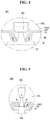
- FIG. 4 is an enlarged view of an area AR 1 shown in FIG. 3 .
- an OLED display includes a display panel including a first substrate SUB 1 and a second substrate SUB 2 facing each other and a conductive filler layer CFL between the first substrate SUB 1 and the second substrate SUB 2 .
- the first substrate SUB 1 is a thin film transistor array substrate on which a thin film transistor T and an organic light emitting diode OLE are disposed.
- the second substrate SUB 2 is a substrate on which a low potential power voltage line (hereinafter referred to as “Evss line”) EVL is disposed.
- the second substrate SUB 2 may function as an encapsulation substrate.
- the first substrate SUB 1 and the second substrate SUB 2 may be attached to each other using a sealant SL.
- the sealant SL is disposed at an edge of the first substrate SUB 1 and an edge of the second substrate SUB 2 and maintains a predetermined distance between the first substrate SUB 1 and the second substrate SUB 2 .
- the conductive filler layer CFL may be disposed inside the sealant SL.
- the first substrate SUB 1 may be made of glass material or plastic material.
- the first substrate SUB 1 may be made of plastic material such as polyimide (PI), polyethylene terephthalate (PET), polyethylene naphthalate (PEN), and polycarbonate (PC) and may have flexible characteristics.
- PI polyimide
- PET polyethylene terephthalate
- PEN polyethylene naphthalate
- PC polycarbonate
- the thin film transistor T and the organic light emitting diode OLE connected to the thin film transistor T are formed on the first substrate SUB 1 .
- a light shielding layer LS and a buffer layer BUF may be formed between the first substrate SUB 1 and the thin film transistor T.
- the light shielding layer LS is disposed to overlap a semiconductor layer, particularly, a channel of the thin film transistor T and can protect an oxide semiconductor element from external light.
- the buffer layer BUF can block ions or impurities diffused from the first substrate SUB 1 and also block moisture penetration from the outside.
- the thin film transistor T includes a semiconductor layer ACT, a gate electrode GE, a source electrode SE, and a drain electrode DE.
- a gate insulating layer GI and the gate electrode GE are disposed on the semiconductor layer ACT.
- the gate insulating layer GI functions to insulate the gate electrode GE and may be formed of silicon oxide (SiOx). However, embodiments are not limited thereto.
- the gate electrode GE is disposed to overlap the semiconductor layer ACT with the gate insulating layer GI interposed therebetween.
- the gate electrode GE may be formed as a single layer or a multilayer using copper (Cu), molybdenum (Mo), aluminum (Al), chrome (Cr), gold (Au), titanium (Ti), nickel (Ni), neodymium (Nd), tantalum (Ta), tungsten (W), or a combination thereof.
- the gate insulating layer GI and the gate electrode GE may be patterned using the same mask. In this instance, the gate insulating layer GI and the gate electrode GE may have the same area. Although not shown, the gate insulating layer GI may be formed to cover the entire surface of the first substrate SUB 1 .
- An interlayer dielectric layer IN is positioned on the gate electrode GE.
- the interlayer dielectric layer IN functions to insulate the gate electrode GE and the source and drain electrodes SE and DE from each other.
- the interlayer dielectric layer IN may be formed of silicon oxide (SiOx), silicon nitride (SiNx), or a multilayer thereof. However, embodiments are not limited thereto.
- the source electrode SE and the drain electrode DE are positioned on the interlayer dielectric layer IN.
- the source electrode SE and the drain electrode DE are spaced from each other by a predetermined distance.
- the source electrode SE contacts one side of the semiconductor layer ACT through a source contact hole penetrating the interlayer dielectric layer IN.
- the drain electrode DE contacts the other side of the semiconductor layer ACT through a drain contact hole penetrating the interlayer dielectric layer IN.
- Each of the source electrode SE and the drain electrode DE may be formed as a single layer or as a multilayer.
- each of the source electrode SE and the drain electrode DE may be formed of molybdenum (Mo), aluminum (Al), chrome (Cr), gold (Au), titanium (Ti), nickel (Ni), neodymium (Nd), copper (Cu), or a combination thereof.
- each of the source electrode SE and the drain electrode DE may be formed as a double layer of Mo/Al—Nd, Mo/Al, Ti/Al or Cu/MoTi, or as a triple layer of Mo/Al—Nd/Mo, Mo/Al/Mo, Ti/Al/Ti or MoTi/Cu/MoTi.
- a passivation layer PAS 1 is positioned on the thin film transistor T.
- the passivation layer PAS 1 protects the thin film transistor T and may be formed of silicon oxide (SiOx), silicon nitride (SiNx), or a multilayer thereof.
- a planarization layer OC is positioned on the passivation layer PAS 1 .
- the planarization layer OC can reduce or planarize a height difference (or step coverage) of an underlying structure and may be formed of an organic material such as photo acryl, polyimide, benzocyclobutene-based resin, and acrylate-based resin. If necessary or desired, one of the passivation layer PAS 1 and the planarization layer OC may be omitted.
- the organic light emitting diode OLE and an auxiliary electrode AE are positioned on the planarization layer OC.
- the organic light emitting diode OLE includes an anode ANO, an organic light emitting layer OL, and a cathode CAT.
- the anode ANO is positioned on the planarization layer OC.
- the anode ANO is connected to the source electrode SE of the thin film transistor T through a contact hole penetrating the passivation layer PAS 1 and the planarization layer OC.
- the anode ANO may include a reflective layer and thus serve as a reflective electrode.
- the reflective layer may be formed of aluminum (Al), copper (Cu), silver (Ag), palladium (Pd), nickel (Ni), or a combination thereof.
- the reflective layer may be formed of Ag/Pd/Cu (APC) alloy.
- the anode ANO may be formed as a multilayer including a reflective layer.
- the auxiliary electrode AE is positioned on the planarization layer OC.
- the auxiliary electrode AE may be formed of the same material as the anode ANO at the same layer as the anode ANO. In this instance, because a separate process for forming the auxiliary electrode AE does not need to be performed, the number of processes can be reduced. Hence, the manufacturing time and the manufacturing cost can be reduced, and product yield can be remarkably improved.
- the auxiliary electrode AE may function to receive a low potential power voltage from the Evss line EVL through the conductive filler layer CFL and transfer the low potential power voltage to the cathode CAT.
- a bank layer BN is positioned on the first substrate SUB 1 , on which the anode ANO and the auxiliary electrode AE are formed, and partitions pixels.
- the bank layer BN may be formed of an organic material such as polyimide, benzocyclobutene-based resin, and acrylate. At least a portion (e.g., center portion) of the anode ANO exposed by a openings of the bank layer BN may be defined as an emission region.
- the bank layer BN may be configured to expose the center portion of the anode ANO and cover an edge of the anode ANO.
- the exposed portion of the anode ANO may be designed to have as large an area as possible, in order to sufficiently secure an aperture ratio.
- the bank layer BN may be configured to expose a center portion of the auxiliary electrode AE and cover an edge of the auxiliary electrode AE.
- the exposed portion of the auxiliary electrode AE may be designed to have as large an area as possible, in order to sufficiently secure a contact area between the auxiliary electrode AE and the conductive filler layer CFL.
- a first barrier BR 1 is positioned on the first substrate SUB 1 on which the bank layer BN is formed.
- the first barrier BR 1 is positioned on the auxiliary electrode AE.
- the first barrier BR 1 functions to physically divide each of the organic light emitting layer OL, the cathode CAT, and a protective layer PAS 2 that will be formed later.
- each of the organic light emitting layer OL, the cathode CAT, and the protective layer PAS 2 is disposed on the auxiliary electrode AE and is physically divided by the first barrier BR 1 .
- each of the organic light emitting layer OL, the cathode CAT, and the protective layer PAS 2 may be discontinuously formed on the auxiliary electrode AE.
- the bank layer BN and the planarization layer OC may be patterned to cover only the thin film transistor T and a storage capacitor Cst connected to the thin film transistor T inside the pixel.
- the storage capacitor Cst may have a triple structure in which first to third capacitor electrodes are stacked.
- embodiments are not limited thereto.
- the storage capacitor Cst may be implemented as a plurality of layers.
- the organic light emitting layer OL is positioned on the first substrate SUB 1 on which the first barrier BR 1 is formed.
- the organic light emitting layer OL may be widely formed on a front surface of the first substrate SUB 1 .
- the organic light emitting layer OL is a layer, in which electrons and holes combine and emit light.
- the organic light emitting layer OL includes an emission layer EML and may further include one or more of a hole injection layer HIL, a hole transport layer HTL, an electron transport layer ETL, and an electron injection layer EIL.
- the emission layer EML may include a light emitting material that generates white light.
- the organic light emitting layer OL emitting white light may have a multi-stack structure, for example, an n-stack structure, where n is an integer equal to or greater than 1.
- 2-stack structure may include a charge generation layer CGL between the anode ANO and the cathode CAT and a first stack and a second stack respectively disposed on and under the charge generation layer CGL.
- Each of the first stack and the second stack includes an emission layer and may further include at least one common layer.
- the emission layer of the first stack and the emission layer of the second stack may include emission materials of different colors, respectively.
- the organic light emitting layer OL on the auxiliary electrode AE is physically divided by the first barrier BR 1 .
- the organic light emitting layer OL is divided by the first barrier BR 1 and exposes at least a portion of the auxiliary electrode AE around the first barrier BR 1 .
- a portion of the organic light emitting layer OL divided by the first barrier BR 1 is positioned on the first barrier BR 1 .
- the cathode CAT is positioned on the organic light emitting layer OL.
- the cathode CAT may be widely formed on the front surface of the first substrate SUB 1 .
- the cathode CAT may be formed of a transparent conductive material such as indium tin oxide (ITO) and indium zinc oxide (IZO).
- ITO indium tin oxide
- IZO indium zinc oxide
- the cathode CAT may be formed of a material, which is thin enough to transmit light, for example, magnesium (Mg), calcium (Ca), aluminum (Al), silver (Ag), or a combination thereof.
- the cathode CAT on the auxiliary electrode AE is physically divided by the first barrier BR 1 .
- the cathode CAT is divided by the first barrier BR 1 and exposes at least a portion of the auxiliary electrode AE around the first barrier BR 1 .
- a portion of the cathode CAT divided by the first barrier BR 1 is positioned on the first barrier BR 1 .
- the cathode CAT may directly contact the auxiliary electrode AE and may be supplied with the low potential power voltage through the auxiliary electrode AE.
- the cathode CAT covers the organic light emitting layer OL, and one end of the cathode CAT directly contacts the auxiliary electrode AE. Namely, one end of the cathode CAT, which is divided by the first barrier BR 1 and is exposed, directly contacts an exposed upper surface of the auxiliary electrode AE.
- Such a structure may be implemented by a step coverage difference between materials forming the organic light emitting layer OL and the cathode CAT.
- the cathode CAT is made of a transparent conductive material having better step coverage than a formation material of the organic light emitting layer OL, the cathode CAT may be configured to directly contact the auxiliary electrode AE.
- the organic light emitting layer OL and the cathode CAT may be formed using different methods.
- the organic light emitting layer OL may be formed using a thermal deposition method
- the cathode CAT may be formed using a sputtering method.
- one end of the divided cathode CAT may be extended further than one end of the divided organic light emitting layer OL and may directly contact the auxiliary electrode AE.
- the protective layer PAS 2 is positioned on the cathode CAT.
- the protective layer PAS 2 may be widely formed on the front surface of the first substrate SUB 1 .
- the protective layer PAS 2 may be formed of a material such as silicon oxide (SiOx) and silicon nitride (SiNx).
- the protective layer PAS 2 is positioned on the cathode CAT and can block the penetration of foreign material that may enter the organic light emitting diode OLE.
- the cathode CAT including a transparent conductive material is a crystalline component and cannot block the penetration of ions and moisture, ionic components or external impurities of an ionic liquid included in the conductive filler layer CFL may pass through the cathode CAT and may enter the organic light emitting layer OL.
- the first embodiment of the disclosure further includes the protective layer PAS 2 on the organic light emitting diode OLE and can block the penetration of foreign material that may enter the organic light emitting diode OLE.
- the first embodiment of the disclosure can prevent a reduction in lifespan of the organic light emitting diode OLE and a luminance reduction.
- the protective layer PAS 2 is positioned on the cathode CAT and can buffer or mitigate a stress applied to the cathode CAT when the first substrate SUB 1 and the second substrate SUB 2 are attached to each other.
- the cathode CAT including the transparent conductive material has brittle characteristics, the cathode CAT may easily crack due to an external force applied.
- the first embodiment of the disclosure further includes the protective layer PAS 2 on the cathode CAT and can prevent a crack from being generated in the cathode CAT. Furthermore, the first embodiment of the disclosure can prevent the penetration of oxygen or moisture due to the crack.
- the protective layer PAS 2 on the auxiliary electrode AE is physically divided by the first barrier BR 1 .
- the protective layer PAS 2 is divided by the first barrier BR 1 and exposes at least a portion of the auxiliary electrode AE around the first barrier BR 1 .
- a portion of the protective layer PAS 2 divided by the first barrier BR 1 is positioned on the first barrier BR 1 .
- the portion of the organic light emitting layer OL, the portion of the cathode CAT, and the portion of the protective layer PAS 2 are sequentially stacked on the first barrier BR 1 .
- the Evss line EVL and a color filter CF are formed on the second substrate SUB 2 .
- a stacking order of the Evss line EVL and the color filter CF on the second substrate SUB 2 may be changed.
- the color filter CF may be formed after the Evss line EVL is formed, or the Evss line EVL may be formed after the color filter CF is formed.
- the Evss line EVL includes a low resistance conductive material.
- the Evss line EVL may be formed of molybdenum (Mo), aluminum (Al), chromium (Cr), gold (Au), titanium (Ti), nickel (Ni), neodymium (Nd), copper (Cu), or a combination thereof.
- the Evss line EVL may include a low reflective conductive material.
- the Evss line EVL is formed of the low reflective conductive material and thus can prevent visibility from being reduced by the reflection of external light.
- a display device does not need to include a separate component for shielding (or absorbing) light incident from outside, like a polarizing film.
- the Evss line EVL may function as a black matrix. Therefore, the Evss line EVL can prevent a defect of color mixture from occurring between neighboring pixels.
- the Evss line EVL may be disposed corresponding to a non-emission region so as to expose at least the emission region.
- the first embodiment of the disclosure can use the Evss line EVL as the black matrix and thus does not need to additionally perform a separate process for forming the black matrix. Therefore, the first embodiment of the disclosure can further reduce the number of processes compared to a related art structure, and thus can reduce the manufacturing time and the manufacturing cost and remarkably improve product yield.
- the color filter CF may include red (R), blue (B), and green (G) color filters.
- the pixel may include subpixels emitting red, blue, and green light, and the color filters CF may be respectively assigned to the corresponding subpixels.
- the red, blue, and green color filters CF may be partitioned by the Evss line EVL. If necessary or desired, the pixel may further include a white (W) subpixel.
- the conductive filler layer CFL is interposed between the first substrate SUB 1 and the second substrate SUB 2 and includes a conductive medium.
- the conductive filler layer CFL may be formed by dispersing conductive fillers in a solvent.
- the conductive filler layer CFL may include a conductive solvent.
- the conductive filler layer CFL may include at least one of a conductive polymer, such as poly(3,4-ethylenedioxythiophene) (PEDOT), and an ionic liquid.
- PEDOT poly(3,4-ethylenedioxythiophene)
- the distance between the first substrate SUB 1 and the second substrate SUB 2 may be appropriately selected depending on viscosity of the conductive filler layer CFL. Because the embodiment of the disclosure uses the conductive fillers having lower viscosity than non-conductive fillers, the distance between the first substrate SUB 1 and the second substrate SUB 2 can be reduced. Hence, the embodiment of the disclosure can secure a wide viewing angle and a high aperture ratio.
- the cathode CAT of the first substrate SUB 1 and the Evss line EVL of the second substrate SUB 2 are electrically connected through the conductive filler layer CFL.
- the low potential power voltage is applied to both the cathode CAT and the Evss line EVL.
- the embodiment of the disclosure because the protective layer PAS 2 is interposed between the conductive filler layer CFL and the cathode CAT, it is difficult to bring the conductive filler layer CFL into direct contact with the cathode CAT without using the first barrier BR 1 .
- the embodiment of the disclosure includes the first barrier BR 1 and thus can expose at least a portion of the auxiliary electrode AE while physically dividing each of the organic light emitting layer OL, the cathode CAT, and the protective layer PAS 2 .
- the exposed portion of the auxiliary electrode AE can directly contact the conductive filler layer CFL to receive the low potential power voltage from the Evss line EVL of the second substrate SUB 2 , and can also directly contact the cathode CAT to transfer the received low potential power voltage to the cathode CAT.
- the first embodiment of the disclosure can reduce a voltage variation (or voltage deviation) depending on a position by connecting the Evss line EVL formed of the low resistance conductive material to the cathode CAT. Hence, the first embodiment of the disclosure can reduce non-uniformity of luminance or a luminance variation (or luminance variation).
- the first embodiment of the disclosure does not need to separately assign an area for forming the Evss line EVL and an area for connecting the Evss line EVL and the cathode CAT to the thin film transistor array substrate, as in the related art. Therefore, the first embodiment of the disclosure can be easily applied to a high-resolution display having a high pixel per inch (PPI) and can remarkably improve a degree of design freedom.
- PPI pixel per inch
- FIG. 5 is an enlarged view of an area AR 2 shown in FIG. 3 .
- the OLED display according to the first embodiment of the disclosure further includes a connection member LM attached to at least one side of the display panel, particularly, at least one side of the first substrate SUB 1 .
- the connection member LM may be a chip-on film (COF).
- COF chip-on film
- the first substrate SUB 1 includes a low potential power voltage pad (hereinafter referred to as “Evss pad”) EVP and a power electrode POE.
- Evss pad EVP is disposed outside the sealant SL and is electrically connected to the connection member LM.
- the power electrode POE is disposed inside the sealant SL and is electrically connected to the conductive filler layer CFL.
- the Evss pad EVP receives the low potential power voltage generated by the power generator (not shown) through the connection member LM and transfers the received low potential power voltage to the power electrode POE.
- the power electrode POE then transfers the low potential power voltage to the conductive filler layer CFL.
- connection member LM, the Evss pad EVP, the power electrode POE, the conductive filler layer CFL, and the cathode CAT may be electrically connected to form a low potential power voltage supply path
- connection member LM, the Evss pad EVP, the power electrode POE, the conductive filler layer CFL, the Evss line EVL, and the cathode CAT may be electrically connected to form a low potential power voltage supply path.
- the Evss pad EVP includes at least one pad electrode.
- the layers may be disposed at different layers with at least one insulating layer interposed therebetween and may be electrically connected through a pad contact hole penetrating the at least one insulating layer.
- the Evss pad EVP may include a first pad electrode PE 1 and a second pad electrode PE 2 that are disposed at different layers with the passivation layer PAS 1 interposed therebetween, and the first pad electrode PE 1 and the second pad electrode PE 2 may be connected to each other through a first pad contact hole PH 1 penetrating the passivation layer PAS 1 .
- the embodiment of the disclosure describes a case where the Evss pad EVP includes the first pad electrode PE 1 and the second pad electrode PE 2 as an example, for convenience of explanation.
- the first pad electrode PE 1 is disposed outside the sealant SL and is exposed to the outside.
- the exposed first pad electrode PE 1 may be attached to the connection member LM.
- the first pad electrode PE 1 and the connection member LM may be attached to each other through an anisotropic conductive film (ACF) layer (not shown) interposed between them.
- ACF anisotropic conductive film
- the second pad electrode PE 2 is extended to the inside of the sealant SL and is electrically connected to the power electrode POE. In this instance, the second pad electrode PE 2 may contact the power electrode POE through a second pad contact hole PH 2 penetrating the passivation layer PAS 1 .
- FIG. 3 illustrates that the second pad electrode PE 2 and the power electrode POE are disposed with only the passivation layer PAS 1 interposed therebetween, by way of example. However, embodiments are not limited thereto.
- the second pad electrode PE 2 and the power electrode POE may be disposed at different layers with the passivation layer PAS 1 and the planarization layer OC interposed therebetween and may be electrically connected to each other through a contact hole penetrating the passivation layer PAS 1 and the planarization layer OC.
- the power electrode POE may be formed together when the anode ANO is formed. Namely, the power electrode POE may be formed of the same material as the anode ANO and the auxiliary electrode AE. However, embodiments are not limited thereto.
- a second barrier BR 2 is positioned on the power electrode POE.
- the second barrier BR 2 may be formed together when the first barrier BR 1 is formed. Namely, the second barrier BR 2 may be formed of the same material as the first barrier BR 1 and may have the same shape as the first barrier BR 1 .
- the second barrier BR 2 functions to physically divide each of the organic light emitting layer OL, the cathode CAT, and the protective layer PAS 2 .
- each of the organic light emitting layer OL, the cathode CAT, and the protective layer PAS 2 is disposed on the auxiliary electrode AE and is physically divided by the second barrier BR 2 .
- each of the organic light emitting layer OL, the cathode CAT, and the protective layer PAS 2 may be discontinuously formed on the auxiliary electrode AE.
- the organic light emitting layer OL, the cathode CAT, and the protective layer PAS 2 are disposed inside the sealant SL and on the entire surface of the first substrate SUB 1 . Therefore, when the second barrier BR 2 is not included, the organic light emitting layer OL, the cathode CAT, and the protective layer PAS 2 are formed to completely cover the power electrode POE positioned inside the sealant SL. In this instance, the power electrode POE and the cathode CAT cannot be electrically connected to each other because of the organic light emitting layer OL, and the power electrode POE and the conductive filler layer CFL cannot be electrically connected to each other because of the organic light emitting layer OL and the protective layer PAS 2 .
- the first embodiment of the disclosure forms the second barrier BR 2 on the power electrode POE and thus can expose at least a portion of the power electrode POE while physically dividing each of the organic light emitting layer OL, the cathode CAT, and the protective layer PAS 2 on the power electrode POE.
- a portion of the organic light emitting layer OL, a portion of the cathode CAT, and a portion of the protective layer PAS 2 , each of which is divided by the second barrier BR 2 are sequentially stacked on the second barrier BR 2 .
- An exposed portion of the power electrode POE directly contacts the conductive filler layer CFL and supplies the low potential power voltage to the conductive filler layer CFL.
- a power supply path connecting the connection member LM, the Evss pad EVP, and the conductive filler layer CFL may be formed.
- the cathode CAT on the power electrode POE may cover the organic light emitting layer OL, and one end of the cathode CAT may directly contact the power electrode POE. Namely, one end of the cathode CAT, which is divided by the second barrier BR 2 and is exposed, may directly contact an exposed upper surface the power electrode POE. Hence, a power supply path connecting the connection member LM, the Evss pad EVP, and the cathode CAT may be formed.
- FIG. 6 is cross-sectional views schematically illustrating a shape of a barrier including first and second barriers.
- a barrier BR may be formed as a double layer including a first structure B 1 and a second structural B 2 .
- the first structure B 1 may be disposed on the second structural B 2 , and an edge of the first structure B 1 may have an eaves shape. Namely, the edge of the first structure B 1 may protrude from an edge of the second structural B 2 to the outside by a predetermined distance RR.
- the distance RR between the edge of the first structure B 1 and the edge of the second structural B 2 may be properly selected so that the barrier BR can expose at least a portion of an auxiliary electrode AE while dividing each of an organic light emitting layer, a cathode, and a protective layer.
- each of the organic light emitting layer OL see FIG.
- the first structure B 1 may have a reverse taper shape as shown in portion (a) of FIG. 6 and may have a taper shape as shown in portion (b) of FIG. 6 .
- the first structure B 1 and the second structural B 2 may be formed of different materials.
- a barrier BR may be formed as a single layer including a first structure B 1 .
- the first structure B 1 has a shape in which an edge of an upper side protrudes from an edge of a lower side to the outside by a predetermined distance RR.
- the first structure B 1 may have a reverse taper shape as shown in portion (c) of FIG. 6 .
- a vertical cross-sectional shape of the first structure B 1 may have a trapezoidal shape
- the upper side may have a length longer than the lower side
- one end of the upper side may protrude from one end of the lower side to the outside by the predetermined distance RR.
- the distance RR between one end of the upper side and one end of the lower side may be properly selected so that the barrier BR can expose at least a portion of an auxiliary electrode AE while dividing each of an organic light emitting layer, a cathode, and a protective layer.
- each of the organic light emitting layer OL (see FIG. 3 ), the cathode CAT (see FIG. 3 ), and the protective layer PAS 2 (see FIG. 3 ) is patterned to expose at least a portion of the auxiliary electrode AE while being divided around the barrier BR due to the distance RR between one end of the upper side and one end of the lower side.
- FIG. 7 is a cross-sectional view of an OLED display according to a second embodiment of the disclosure. Description of structures and components identical or equivalent to those illustrated in the first embodiment is omitted in the second embodiment.
- an OLED display includes a first substrate SUB 1 and a second substrate SUB 2 facing each other and a conductive filler layer CFL between the first substrate SUB 1 and the second substrate SUB 2 .
- the first substrate SUB 1 is a thin film transistor array substrate on which a thin film transistor T and an organic light emitting diode OLE connected to the thin film transistor T are formed.
- the second substrate SUB 2 is a substrate on which an Evss line EVL is formed.
- a color filter CF according to the second embodiment of the disclosure is formed on the first substrate SUB 1 .
- the thin film transistor T and the organic light emitting diode OLE connected to the thin film transistor T are formed on the first substrate SUB 1
- the color filter CF is formed on the organic light emitting diode OLE.
- the second embodiment of the disclosure can further reduce a distance between the color filter CF and an organic light emitting layer OL compared to the first embodiment, and thus can increase a viewing angle and sufficiently secure an aperture ratio.
- the color filter CF may be interposed between a cathode CAT constituting the organic light emitting diode OLE and a protective layer PAS 2 , or may be disposed on the protective layer PAS 2 .
- the color filter CF may be disposed on the protective layer PAS 2 . In this case, it is possible to minimize or reduce the deterioration of the organic light emitting diode OLE that may occur due to exposure to the process environment for forming the color filter CF.
- FIG. 8 is a cross-sectional view of an OLED display according to a third embodiment of the disclosure. Description of structures and components identical or equivalent to those illustrated in the first and second embodiments is omitted in the third embodiment.
- an OLED display includes a first substrate SUB 1 and a second substrate SUB 2 facing each other and a conductive filler layer CFL between the first substrate SUB 1 and the second substrate SUB 2 .
- the first substrate SUB 1 is a thin film transistor array substrate on which a thin film transistor T and an organic light emitting diode OLE connected to the thin film transistor T are formed.
- the second substrate SUB 2 is a substrate on which an Evss line EVL is formed.
- the Evss line EVL and an auxiliary Evss line (or referred to as “auxiliary power line”) AEVL are formed on the second substrate SUB 2 .
- a color filter CF may be positioned on the second substrate SUB 2 as in the first embodiment and may be positioned on the first substrate SUB 1 as in the second embodiment.
- the auxiliary Evss line AEVL is a power line for increasing a contact area between the Evss line EVL and the conductive filler layer CFL and may have an area larger than the Evss line EVL.
- the auxiliary Evss line AEVL may be interposed between the Evss line EVL and the conductive filler layer CFL.
- the auxiliary Evss line AEVL may be formed to cover the Evss line EVL and the color filter CF and may be widely formed on a front surface of the second substrate SUB 2 including an emission region.
- the auxiliary Evss line AEVL may be formed of a transparent conductive material such as indium tin oxide (ITO) and indium zinc oxide (IZO).
- the third embodiment of the disclosure can sufficiently secure the contact area between the Evss line EVL and the conductive filler layer CFL using the auxiliary Evss line AEVL, the third embodiment of the disclosure can minimize or reduce a contact failure between the Evss line EVL and the conductive filler layer CFL. Further, the third embodiment of the disclosure can more efficiently reduce a voltage variation depending on a position and thus can reduce non-uniformity of luminance or a luminance variation.
- FIG. 9 is a cross-sectional view of an OLED display according to a fourth embodiment of the disclosure.
- FIGS. 10 and 11 enlargedly illustrate an area AR 3 shown in FIG. 9 .
- FIG. 12 illustrates a position relationship of a spacer, an Evss line, and an auxiliary Evss line. Description of structures and components identical or equivalent to those illustrated in the first to third embodiments is omitted in the fourth embodiment.
- a cathode CAT of a first substrate SUB 1 and an Evss line EVL of a second substrate SUB 2 are electrically connected to each other through a conductive filler layer CFL.
- the Evss line EVL can transfer a low potential power voltage to the cathode CAT through the conductive filler layer CFL.
- the cathode CAT does not directly contact the conductive filler layer CFL and receives the low potential power voltage from the conductive filler layer CFL through an auxiliary electrode AE.
- the auxiliary electrode AE of the first substrate SUB 1 and the Evss line EVL of the second substrate SUB 2 are spaced from each other by an attachment distance between the first substrate SUB 1 and the second substrate SUB 2 and are also electrically connected to each other through the conductive filler layer CFL between the first substrate SUB 1 and the second substrate SUB 2 . Therefore, it may be difficult to perform the supply of power voltage due to a resistance of the conductive filler layer CFL. More specifically, because an influence of the resistance increases corresponding to a distance between the auxiliary electrode AE and the Evss line EVL, it may be difficult to perform the supply of the power voltage from the Evss line EVL to the auxiliary electrode AE.
- the fourth embodiment of the disclosure proposes a method capable of reducing the problem of the supply of the power voltage.
- the fourth embodiment of the disclosure forms a spacer SP on the second substrate SUB 2 , in order to reduce a distance between the auxiliary electrode AE and the Evss line EVL.
- the spacer SP has a shape protruding toward the first substrate SUB 1 .
- the spacer SP may be formed of an organic material such as polyimide, benzocyclobutene-based resin, and acrylate. However, embodiments are not limited thereto.
- the spacer SP is disposed adjacent to the auxiliary electrode AE. To this end, the spacer SP may be disposed to overlap the auxiliary electrode AE in an up-down direction.
- the Evss line EVL is extended to cover the spacer SP.
- FIG. 9 illustrates that the Evss line EVL completely covers the spacer SP, by way of example.
- the Evss line EVL may be extended to cover at least a portion of the spacer SP, so that the Evss line EVL is disposed adjacent to the auxiliary electrode AE of the first substrate SUB 1 .
- the Evss line EVL may be extended up to a most protruding portion (e.g., an upper surface) of the spacer SP, so that the Evss line EVL is positioned as close as possible to the auxiliary electrode AE.
- the fourth embodiment of the disclosure may further include an auxiliary Evss line AEVL as in the third embodiment.
- the auxiliary Evss line AEVL may be extended to cover the spacer SP.
- FIG. 11 illustrates that the auxiliary Evss line AEVL completely covers the spacer SP, by way of example.
- the auxiliary Evss line AEVL may be extended to cover at least a portion of the spacer SP, so that the auxiliary Evss line AEVL is disposed adjacent to the auxiliary electrode AE of the first substrate SUB 1 .
- auxiliary Evss line AEVL may be extended up to a most protruding portion (e.g., an upper surface) of the spacer SP, so that the auxiliary Evss line AEVL is positioned as close as possible to the auxiliary electrode AE.
- both the Evss line EVL and the auxiliary Evss line AEVL may be sequentially disposed on the spacer SP.
- the spacer SP may be interposed between the Evss line EVL and the auxiliary Evss line AEVL. More specifically, the spacer SP may be disposed on the Evss line EVL, and the auxiliary Evss line AEVL may be disposed to cover at least a portion of the spacer SP.
- the fourth embodiment of the disclosure includes the spacer SP and thus can set a distance between the Evss line EVL and the auxiliary electrode AE and/or a distance between the auxiliary Evss line AEVL and the auxiliary electrode AE to a minimum or a reduced value possible in the process.
- the fourth embodiment of the disclosure can reduce the above-described influence of resistance and stably supply the power voltage to the cathode CAT.
- the spacer SP may be positioned opposite a first barrier BR 1 . More specifically, when an external force is provided for the OLED display, the OLED display may be pressurized by the external force and may reduce the attachment distance between the first substrate SUB 1 and the second substrate SUB 2 at a specific position. In this instance, a protective layer PAS 2 may be damaged by the spacer SP protruding toward the second substrate SUB 2 and may cause a defect such as the penetration of foreign material into an organic light emitting diode OLE. In order to prevent this, the spacer SP may overlap the first barrier BR 1 and may be disposed opposite the first barrier BR 1 . In this instance, because the spacer SP contacts the first barrier BR 1 or moves on the first barrier BR 1 by the provided external force, a direct contact between the spacer SP and the protective layer PAS 2 can be prevented. Hence, product reliability can be secured.
Landscapes
- Physics & Mathematics (AREA)
- Optics & Photonics (AREA)
- Engineering & Computer Science (AREA)
- Microelectronics & Electronic Packaging (AREA)
- Computer Hardware Design (AREA)
- General Physics & Mathematics (AREA)
- Power Engineering (AREA)
- Theoretical Computer Science (AREA)
- Condensed Matter Physics & Semiconductors (AREA)
- Electroluminescent Light Sources (AREA)
- Devices For Indicating Variable Information By Combining Individual Elements (AREA)
- Illuminated Signs And Luminous Advertising (AREA)
- Control Of El Displays (AREA)
Applications Claiming Priority (2)
| Application Number | Priority Date | Filing Date | Title |
|---|---|---|---|
| KR1020170147595A KR102423799B1 (ko) | 2017-11-07 | 2017-11-07 | 유기발광 표시장치 |
| KR10-2017-0147595 | 2017-11-07 |
Publications (2)
| Publication Number | Publication Date |
|---|---|
| US20190140037A1 US20190140037A1 (en) | 2019-05-09 |
| US10559646B2 true US10559646B2 (en) | 2020-02-11 |
Family
ID=66327572
Family Applications (1)
| Application Number | Title | Priority Date | Filing Date |
|---|---|---|---|
| US16/180,451 Active US10559646B2 (en) | 2017-11-07 | 2018-11-05 | Organic light emitting diode display having barrier layer on auxiliary electrode |
Country Status (2)
| Country | Link |
|---|---|
| US (1) | US10559646B2 (ko) |
| KR (1) | KR102423799B1 (ko) |
Cited By (1)
| Publication number | Priority date | Publication date | Assignee | Title |
|---|---|---|---|---|
| US11737329B2 (en) | 2020-05-12 | 2023-08-22 | Samsung Display Co., Ltd. | Display apparatus having column spacer between emission panel and color panel |
Families Citing this family (6)
| Publication number | Priority date | Publication date | Assignee | Title |
|---|---|---|---|---|
| KR102489043B1 (ko) * | 2017-12-27 | 2023-01-16 | 엘지디스플레이 주식회사 | 유기발광 표시장치 |
| CN110579913B (zh) * | 2019-08-09 | 2020-12-04 | 武汉华星光电半导体显示技术有限公司 | 显示面板及显示装置 |
| CN110610972B (zh) * | 2019-09-19 | 2022-06-03 | 京东方科技集团股份有限公司 | 一种显示基板及其制备方法、显示装置 |
| KR20210086292A (ko) * | 2019-12-31 | 2021-07-08 | 엘지디스플레이 주식회사 | 표시 장치와 이를 이용한 멀티 표시 장치 |
| CN111554720B (zh) * | 2020-05-15 | 2022-11-04 | 京东方科技集团股份有限公司 | 显示基板及其制备方法、显示装置 |
| CN114203787A (zh) * | 2021-12-10 | 2022-03-18 | 深圳市华星光电半导体显示技术有限公司 | 一种显示面板及其制备方法 |
Citations (5)
| Publication number | Priority date | Publication date | Assignee | Title |
|---|---|---|---|---|
| US20140183502A1 (en) * | 2013-01-02 | 2014-07-03 | Samsung Display Co., Ltd. | Organic light emitting diode display |
| US20160013438A1 (en) * | 2014-07-08 | 2016-01-14 | Lg Display Co., Ltd. | Organic light emitting display device and manufacturing method thereof |
| US20160149164A1 (en) * | 2014-11-26 | 2016-05-26 | Lg Display Co., Ltd. | Organic light emitting display device and fabricating method using the same |
| US20180006106A1 (en) * | 2016-07-04 | 2018-01-04 | Samsung Display Co., Ltd. | Organic light emitting display device and method for manufacturing same |
| US20180374909A1 (en) * | 2017-06-23 | 2018-12-27 | Joled Inc. | Organic el display panel and organic el display panel manufacturing method |
-
2017
- 2017-11-07 KR KR1020170147595A patent/KR102423799B1/ko active IP Right Grant
-
2018
- 2018-11-05 US US16/180,451 patent/US10559646B2/en active Active
Patent Citations (5)
| Publication number | Priority date | Publication date | Assignee | Title |
|---|---|---|---|---|
| US20140183502A1 (en) * | 2013-01-02 | 2014-07-03 | Samsung Display Co., Ltd. | Organic light emitting diode display |
| US20160013438A1 (en) * | 2014-07-08 | 2016-01-14 | Lg Display Co., Ltd. | Organic light emitting display device and manufacturing method thereof |
| US20160149164A1 (en) * | 2014-11-26 | 2016-05-26 | Lg Display Co., Ltd. | Organic light emitting display device and fabricating method using the same |
| US20180006106A1 (en) * | 2016-07-04 | 2018-01-04 | Samsung Display Co., Ltd. | Organic light emitting display device and method for manufacturing same |
| US20180374909A1 (en) * | 2017-06-23 | 2018-12-27 | Joled Inc. | Organic el display panel and organic el display panel manufacturing method |
Cited By (1)
| Publication number | Priority date | Publication date | Assignee | Title |
|---|---|---|---|---|
| US11737329B2 (en) | 2020-05-12 | 2023-08-22 | Samsung Display Co., Ltd. | Display apparatus having column spacer between emission panel and color panel |
Also Published As
| Publication number | Publication date |
|---|---|
| KR20190051690A (ko) | 2019-05-15 |
| KR102423799B1 (ko) | 2022-07-22 |
| US20190140037A1 (en) | 2019-05-09 |
Similar Documents
| Publication | Publication Date | Title |
|---|---|---|
| US10930718B2 (en) | Organic light emitting diode display having barrier layer on auxiliary electrode | |
| US10559646B2 (en) | Organic light emitting diode display having barrier layer on auxiliary electrode | |
| US10692958B2 (en) | Organic light emitting diode display | |
| US10686022B2 (en) | Organic light emitting diode display | |
| US10566407B2 (en) | Organic light emitting diode display having barrier layer on auxiliary electrode | |
| US10971700B2 (en) | Organic light emitting diode display | |
| US10535724B2 (en) | Organic light emitting diode display | |
| CN109887954B (zh) | 有机发光二极管显示器 | |
| US10644097B2 (en) | Organic light emitting diode display device |
Legal Events
| Date | Code | Title | Description |
|---|---|---|---|
| AS | Assignment |
Owner name: LG DISPLAY CO., LTD., KOREA, REPUBLIC OF Free format text: ASSIGNMENT OF ASSIGNORS INTEREST;ASSIGNORS:LEE, JOONSUK;KIM, SEJUNE;REEL/FRAME:047411/0698 Effective date: 20181010 |
|
| FEPP | Fee payment procedure |
Free format text: ENTITY STATUS SET TO UNDISCOUNTED (ORIGINAL EVENT CODE: BIG.); ENTITY STATUS OF PATENT OWNER: LARGE ENTITY |
|
| STPP | Information on status: patent application and granting procedure in general |
Free format text: DOCKETED NEW CASE - READY FOR EXAMINATION |
|
| STPP | Information on status: patent application and granting procedure in general |
Free format text: NON FINAL ACTION MAILED |
|
| STPP | Information on status: patent application and granting procedure in general |
Free format text: NOTICE OF ALLOWANCE MAILED -- APPLICATION RECEIVED IN OFFICE OF PUBLICATIONS |
|
| STPP | Information on status: patent application and granting procedure in general |
Free format text: PUBLICATIONS -- ISSUE FEE PAYMENT RECEIVED |
|
| STCF | Information on status: patent grant |
Free format text: PATENTED CASE |
|
| MAFP | Maintenance fee payment |
Free format text: PAYMENT OF MAINTENANCE FEE, 4TH YEAR, LARGE ENTITY (ORIGINAL EVENT CODE: M1551); ENTITY STATUS OF PATENT OWNER: LARGE ENTITY Year of fee payment: 4 |