US10559585B2 - Vertical memory devices with conductive pads supported by dummy channels with varying dimensions - Google Patents
Vertical memory devices with conductive pads supported by dummy channels with varying dimensions Download PDFInfo
- Publication number
- US10559585B2 US10559585B2 US15/871,478 US201815871478A US10559585B2 US 10559585 B2 US10559585 B2 US 10559585B2 US 201815871478 A US201815871478 A US 201815871478A US 10559585 B2 US10559585 B2 US 10559585B2
- Authority
- US
- United States
- Prior art keywords
- channel structures
- conductive pads
- dummy channel
- conductive
- memory device
- Prior art date
- Legal status (The legal status is an assumption and is not a legal conclusion. Google has not performed a legal analysis and makes no representation as to the accuracy of the status listed.)
- Active
Links
Images


Classifications
-
- H—ELECTRICITY
- H10—SEMICONDUCTOR DEVICES; ELECTRIC SOLID-STATE DEVICES NOT OTHERWISE PROVIDED FOR
- H10B—ELECTRONIC MEMORY DEVICES
- H10B43/00—EEPROM devices comprising charge-trapping gate insulators
- H10B43/30—EEPROM devices comprising charge-trapping gate insulators characterised by the memory core region
- H10B43/35—EEPROM devices comprising charge-trapping gate insulators characterised by the memory core region with cell select transistors, e.g. NAND
-
- H—ELECTRICITY
- H10—SEMICONDUCTOR DEVICES; ELECTRIC SOLID-STATE DEVICES NOT OTHERWISE PROVIDED FOR
- H10B—ELECTRONIC MEMORY DEVICES
- H10B43/00—EEPROM devices comprising charge-trapping gate insulators
- H10B43/10—EEPROM devices comprising charge-trapping gate insulators characterised by the top-view layout
-
- H—ELECTRICITY
- H10—SEMICONDUCTOR DEVICES; ELECTRIC SOLID-STATE DEVICES NOT OTHERWISE PROVIDED FOR
- H10B—ELECTRONIC MEMORY DEVICES
- H10B43/00—EEPROM devices comprising charge-trapping gate insulators
- H10B43/20—EEPROM devices comprising charge-trapping gate insulators characterised by three-dimensional arrangements, e.g. with cells on different height levels
- H10B43/23—EEPROM devices comprising charge-trapping gate insulators characterised by three-dimensional arrangements, e.g. with cells on different height levels with source and drain on different levels, e.g. with sloping channels
- H10B43/27—EEPROM devices comprising charge-trapping gate insulators characterised by three-dimensional arrangements, e.g. with cells on different height levels with source and drain on different levels, e.g. with sloping channels the channels comprising vertical portions, e.g. U-shaped channels
-
- H01L27/11582—
-
- H—ELECTRICITY
- H01—ELECTRIC ELEMENTS
- H01L—SEMICONDUCTOR DEVICES NOT COVERED BY CLASS H10
- H01L23/00—Details of semiconductor or other solid state devices
- H01L23/52—Arrangements for conducting electric current within the device in operation from one component to another, i.e. interconnections, e.g. wires, lead frames
- H01L23/522—Arrangements for conducting electric current within the device in operation from one component to another, i.e. interconnections, e.g. wires, lead frames including external interconnections consisting of a multilayer structure of conductive and insulating layers inseparably formed on the semiconductor body
- H01L23/5226—Via connections in a multilevel interconnection structure
-
- H01L27/11556—
-
- H01L27/11565—
-
- H01L27/11575—
-
- H—ELECTRICITY
- H10—SEMICONDUCTOR DEVICES; ELECTRIC SOLID-STATE DEVICES NOT OTHERWISE PROVIDED FOR
- H10B—ELECTRONIC MEMORY DEVICES
- H10B41/00—Electrically erasable-and-programmable ROM [EEPROM] devices comprising floating gates
- H10B41/20—Electrically erasable-and-programmable ROM [EEPROM] devices comprising floating gates characterised by three-dimensional arrangements, e.g. with cells on different height levels
- H10B41/23—Electrically erasable-and-programmable ROM [EEPROM] devices comprising floating gates characterised by three-dimensional arrangements, e.g. with cells on different height levels with source and drain on different levels, e.g. with sloping channels
- H10B41/27—Electrically erasable-and-programmable ROM [EEPROM] devices comprising floating gates characterised by three-dimensional arrangements, e.g. with cells on different height levels with source and drain on different levels, e.g. with sloping channels the channels comprising vertical portions, e.g. U-shaped channels
-
- H—ELECTRICITY
- H10—SEMICONDUCTOR DEVICES; ELECTRIC SOLID-STATE DEVICES NOT OTHERWISE PROVIDED FOR
- H10B—ELECTRONIC MEMORY DEVICES
- H10B43/00—EEPROM devices comprising charge-trapping gate insulators
- H10B43/50—EEPROM devices comprising charge-trapping gate insulators characterised by the boundary region between the core and peripheral circuit regions
-
- H—ELECTRICITY
- H10—SEMICONDUCTOR DEVICES; ELECTRIC SOLID-STATE DEVICES NOT OTHERWISE PROVIDED FOR
- H10D—INORGANIC ELECTRIC SEMICONDUCTOR DEVICES
- H10D84/00—Integrated devices formed in or on semiconductor substrates that comprise only semiconducting layers, e.g. on Si wafers or on GaAs-on-Si wafers
- H10D84/01—Manufacture or treatment
- H10D84/0123—Integrating together multiple components covered by H10D12/00 or H10D30/00, e.g. integrating multiple IGBTs
- H10D84/0126—Integrating together multiple components covered by H10D12/00 or H10D30/00, e.g. integrating multiple IGBTs the components including insulated gates, e.g. IGFETs
- H10D84/0149—Manufacturing their interconnections or electrodes, e.g. source or drain electrodes
-
- H10W20/42—
Definitions
- Example embodiments relate to vertical memory devices. More particularly, example embodiments relate to vertical NAND flash memory devices.
- a vertical memory device including a plurality of memory cells vertically stacked at a plurality of levels, respectively, on a substrate has been developed. As the number of the levels increases, the vertical memory device may have an unstable structure.
- Example embodiments can provide vertical memory devices having a structure with improved stability.
- a vertical memory device includes a conductive pattern structure on a substrate and comprising a stack of interleaved conductive patterns and insulation layers, wherein edges of the conductive patterns are disposed at spaced apart points along a first direction to provide conductive pads arranged as respective steps in a staircase arrangement.
- a plurality of channel structures extends through the conductive pattern structure in a second direction perpendicular to the first direction, and a plurality of dummy channel structures extends through the first conductive pads in the second direction.
- Respective contact plugs are disposed on the conductive pads.
- a first one of the first conductive pads has a first number of the dummy channel structures passing therethrough and a second one of the first conductive pads has a second number of the dummy channel structures passing therethrough that is different from the first number of the dummy channel structures.
- the dummy channel structures passing through the first one of the conductive pads may have a first width
- the dummy channel structures passing through the second one of the conductive pads may have a second width different than the first width.
- the first number of dummy channel structures may be less that the second number of the dummy channel structures and the first width may be greater than the second width.
- a vertical memory device includes a conductive pattern structure on a first region of a substrate, the conductive pattern structure including a stack of interleaved conductive patterns and insulation layers.
- a pad structure is disposed on a second region of the substrate adjacent the first region of the substrate wherein edges of the conductive patterns are disposed at spaced apart points along a first direction to provide conductive pads arranged as respective steps in a staircase arrangement.
- a plurality of channel structures extends through the conductive pattern structure and a plurality of dummy channel structures extends through the pad structure.
- Respective contact plugs are disposed on the conductive pads. Numbers of the dummy channel structures per unit area passing through the conductive pads vary. Widths of the dummy channel structures passing through the conductive pads may also vary. For example, widths of the dummy channel structures passing though the conductive pads may vary in inverse proportion to the number of the dummy channel structures passing through the conductive pads.
- a vertical memory device includes a conductive pattern structure on a substrate and comprising a stack of interleaved conductive patterns and insulation layers, wherein edges of the conductive patterns are disposed at spaced apart points along a first direction to provide conductive pads arranged as respective steps in a staircase arrangement.
- a plurality of channel structures extends through the conductive pattern structure in a second direction perpendicular to the first direction and a plurality of dummy channel structures extends through the first conductive pads in the second direction.
- Respective contact plugs are disposed on the conductive pads.
- a first one of the first conductive pads has first ones of the dummy channel structures passing therethrough having a first width.
- a second one of the first conductive pads has second ones of the dummy channel structures passing therethrough having a second width different from the first width. Widths of the dummy channel structures may increase from an uppermost one of the conductive pads toward a lowermost one of the conductive pads, and numbers of the dummy channel structures passing through respective ones of the conductive pads may decrease from the uppermost one of the conductive pads toward the lowermost one of the conductive pads.
- the vertical memory device may have a stable structure by arrangement of the dummy channel structures.
- FIGS. 1 to 20 represent non-limiting, example embodiments as described herein.
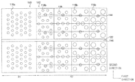
- FIGS. 1A and 2 are a plan view and a cross-sectional view, respectively, illustrating a vertical memory device in accordance with example embodiments;
- FIG. 1B is a plan view illustrating a vertical memory device in accordance with example embodiments
- FIGS. 3 to 15 are cross-sectional views, plan views and a perspective view illustrating stages of a method of manufacturing a vertical memory device in accordance with example embodiments;
- FIGS. 16 and 17 are a plan view and a cross-sectional view, respectively, illustrating a vertical memory device in accordance with example embodiments
- FIG. 18 is a plan view illustrating a vertical memory device in accordance with example embodiments.
- FIG. 19 is a plan view illustrating an arrangement of memory cells in a vertical memory device in accordance with example embodiments.
- FIG. 20 is a plan view illustrating a vertical memory device in accordance with example embodiments.
- FIGS. 1A and 2 are a plan view and a cross-sectional view, respectively, illustrating a vertical memory device in accordance with example embodiments.
- FIG. 1B is a plan view illustrating a vertical memory device in accordance with example embodiments.
- a substrate 100 may include a first region R 1 on which memory cells may be formed in three dimensions and a second region R 2 on which wirings connected with the memory cells may be formed.
- the second region R 2 may be adjacent to edge portions of the first region R 1 in a first direction.
- a conductive pattern structure 140 and a channel structure 118 a may be formed on the first region R 1 .
- a pad structure 142 , a dummy channel structure 118 b and a contact plug 144 may be formed on the second region R 2 .
- the conductive pattern structure 140 and the channel structure 118 a are components of a plurality of memory cells.
- the pad structure 142 may serve as wirings for conveying electrical signals to and from the conductive pattern structure 140 .
- the substrate 100 may include a semiconductor material.
- the substrate 100 may include, for example, a silicon substrate, a germanium substrate or a silicon-germanium substrate.
- the conductive pattern structure 140 may include conductive patterns 126 and insulation layers 102 alternately stacked in an interleaved manner.
- the conductive patterns 126 may be spaced apart along a third direction substantially perpendicular to an upper surface of the substrate 100 .
- the conductive pattern structure 140 may extend in the first direction.
- a plurality of conductive pattern structures 140 may be spaced apart along a second direction substantially perpendicular to the first direction.
- the conductive patterns 126 in the conductive pattern structure 140 may include a ground selection line (GSL), a string selection line (SSL) and a plurality of word lines between the GSL and SSL.
- GSL ground selection line
- SSL string selection line
- the conductive pattern 126 may include a metal.
- the conductive pattern 126 may include a metal pattern and a barrier pattern.
- the metal pattern may include, for example, tungsten, copper, cobalt, aluminum, etc.
- the barrier pattern may include, for example, titanium, titanium nitride, tantalum, tantalum nitride, etc.
- the pad structure 142 may contact edge portions of the conductive pattern structure 140 .
- the conductive pattern structure 140 and the pad structure 142 may be merged into a single body extending along the first direction.
- the pad structure 142 may include the interleaved conductive patterns 126 and insulation layers 102 .
- the conductive patterns 126 in the pad structure 142 and the conductive patterns 126 in the conductive pattern structure 140 may be merged into a single body including substantially the same material.
- the insulation layers 102 in the pad structure 142 and the insulation layers 102 in the conductive pattern structure 140 may be merged into a single body including substantially the same material.
- an edge portion of the pad structure 142 may have a staircase arrangement.
- edges of the conductive patterns 126 may be arranged in a staircase configuration shape, where the conductive patterns 126 have different levels in the third direction.
- the edges of the conductive patterns 126 having the different levels may serve as pads on which contact plugs may be formed, respectively.
- the number of the pads in the pad structure 142 may be substantially the same as the number of the stacked conductive patterns 126 in the conductive pattern structure 140 .
- the pad structure 142 may include step portions in each of the first and second directions.
- the pad structure 142 may include 4 steps disposed at 4 levels, respectively, in the first direction, and 2 steps disposed at 2 sub-levels, respectively, in each level in the second direction.
- the pad structure 142 may have 8 steps at 8 different sub-levels, respectively.
- eight conductive patterns 126 may be stacked in the first region R 1 .
- a first upper insulating interlayer 108 may cover the pad structure 142 .
- a second upper insulating interlayer 109 may be formed on the first upper insulating interlayer 108 and the conductive pattern structure 140 .
- each of the first and second upper insulating interlayers 108 and 109 may be substantially flat.
- a thickness of the first and second upper insulating interlayers 108 and 109 on the pad structure 142 may be greater than a thickness of the second upper insulating interlayer 109 on the conductive pattern structure 140 .
- the channel structures 118 a may extend through the conductive pattern structure 140 , and may have a pillar shape.
- the dummy channel structures 118 b may extend through the first upper insulating interlayer 108 and the pad structure 142 , and may have a pillar shape.
- respective semiconductor patterns 114 may be formed between the substrate 100 and respective ones of the channel structures 118 a .
- Respective semiconductor patterns 114 may be also formed between the substrate 100 and respective ones of the dummy channel structures 118 b .
- each of the channel structures 118 a and the dummy channel structures 118 b may be formed on the respective semiconductor patterns 114 .
- each of the channel structures 118 a and the dummy channel structures 118 b may directly contact the substrate 100 , i.e., the semiconductor patterns 114 may be eliminated.
- each of the channel structures 118 a and the dummy channel structures 118 b may include a dielectric structure 116 a , a channel 116 b and a filling insulation pattern 116 c .
- the channel 116 b may have a hollow cylindrical shape or a cup-like shape.
- the channel 116 b may include polysilicon or single crystalline silicon.
- a portion of the channel 116 b may be doped with p-type impurities, e.g., boron.
- the filling insulation pattern 116 c may be formed on the channel 116 b to fill an inner space of the channel 116 b .
- the filling insulation pattern 116 c may include an insulation material, e.g., silicon oxide.
- the channel 116 b may have a solid cylindrical shape or a pillar shape.
- the filling insulation pattern 116 c may be absent.
- the dielectric structure 116 a may surround an outer sidewall of the channel 116 b .
- the dielectric structure 116 a may include a tunnel insulation layer, a charge storage layer and a blocking dielectric layer layered on the outer sidewall of the channel 116 b .
- the blocking dielectric layer may include an oxide, e.g., silicon oxide, or a metal oxide, e.g., hafnium oxide or aluminum oxide.
- the charge storage layer may include a nitride, e.g., silicon nitride, or a metal oxide.
- the tunnel insulation layer may include an oxide, e.g., silicon oxide.
- the semiconductor pattern 114 may include, for example, polysilicon or single crystalline silicon.
- the channel structures 118 a and the dummy channel structures 118 b may further include an upper conductive pattern 120 on the dielectric structure 116 a , the channel 116 b and the filling insulation pattern 116 c .
- the upper conductive pattern 120 may include, for example, polysilicon.
- the channel structures 118 a may have a first width.
- the channel structures 118 a may have a uniform width.
- the dummy channel structures 118 b may have widths that vary based on the positions thereof.
- Each of the dummy channel structures 118 b may have a width substantially the same as or greater than the first width.
- the number of the dummy channel structures 118 b per a unit area may vary. For example, where widths of the dummy channel structures 118 b at a specific step are relatively great, the number of the dummy channel structures 118 b formed at the specific step may decrease.
- Widths of dummy channel structures 118 b may gradually increase from the portion of the pad structure 142 adjacent to the first region R 1 to the edge portion of the pad structure 142 .
- the widths of dummy channel structures 118 b may gradually increase from the upper steps to the lower steps in the first direction.
- the number of the dummy channel structures 118 b may be gradually decrease from the upper steps to the lower steps in the first direction.
- the number of the dummy channel structures 118 b formed at the respective steps may be different.
- the number of the dummy channel structures 118 b formed at adjacent steps may be equal to each other.
- adjacent steps in the first direction may define a step group, with first, second, third and fourth step groups G 1 , G 2 , G 3 and G 4 are shown in FIG. 1B .
- the number of the dummy channel structures 118 b formed at adjacent steps in each of the first to fourth step groups G 1 , G 2 , G 3 and G 4 may be equal to each other.
- the pad structure 142 includes 40 steps in the first direction
- 10 steps in the first direction may be included in one step group.
- the number of the dummy channel structures 118 b formed at respective first to ten steps in the first step group G 1 may be equal to each other. In the same manner, the number of the dummy channel structures 118 b formed at respective steps in each of the second to fourth step groups G 2 , G 3 and G 4 may be equal. In the pad structure 142 , the number of the dummy channel structures 118 b may gradually increase from the first step group G 1 to the fourth step group G 4 .
- the contact plugs 144 may pass through the first and second upper insulating interlayers 108 and 109 and contact upper surfaces of the conductive patterns 126 in the pad structure 142 .
- the contact plugs 144 may be formed on respective ones of the steps.
- the contact plugs 144 may each include a barrier pattern and a metal pattern.
- the contact plugs 144 may be formed on central portions of the steps. Thus, the contact plugs 144 may be arranged substantially along lines in the first direction and the second direction.
- the pad structure 142 As described above, in the pad structure 142 , as widths of the dummy channel structures 118 b formed at the respective steps increase, the number of the dummy channel structures 118 b formed at the respective steps may decrease. Thus, in the steps in the first direction of the pad structure 142 , remaining areas not occupied by the contact plugs 144 and the dummy channel structures 118 b may be substantially the same. In other words, exposed upper surfaces of the conductive patterns 126 in the pad structure 142 may have substantially the same area. A wiring line (not shown) may be further formed on the contact plug 144 .
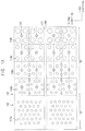
- FIGS. 3 to 15 are cross-sectional views, plan views and perspective views illustrating stages of a method of manufacturing a vertical memory device in accordance with example embodiments. More particularly, FIGS. 3, 4, 7, 9, 12, 13 and 14 are cross-sectional views, FIGS. 5, 8, 10 and 15 are plan views, and FIGS. 6 and 11 are perspective views.
- a preliminary mold structure 106 may be formed on first and second regions R 1 and R 2 of a substrate 100 . Insulation layers 102 and sacrificial layers 104 may be alternately formed on the substrate 100 to form the preliminary mold structure 106 .
- a lowermost insulation layer 102 may serve as a pad insulation layer.
- An uppermost insulation layer 102 may have a thickness greater than other insulation layers 102 in the preliminary mold structure 106 .
- the insulation layers 102 may be formed of an oxide-based material, e.g., silicon oxide, SiC, SiOF, etc.
- the sacrificial layers 104 may be formed of a nitride-based material, e.g., silicon nitride and/or silicon boronitride.
- edge portions of the preliminary mold structure 106 on the second region R 2 may be sequentially etched to form a preliminary step mold structure 106 a .
- the preliminary step mold structure 106 a on the second region R 2 may have a staircase arrangement in each of the first and second directions.
- the sacrificial layers 104 of the preliminary step mold structure 106 a on the first region R 1 may be transformed into conductive patterns of memory cells by subsequent processes.
- each of the steps will serve as pads electrically connected to the conductive patterns of the memory cells that are formed by subsequent processes.
- the number of the steps may be equal to the number of the steps of the stacked sacrificial layers 104 .
- the number of the steps in the first direction may decrease.
- the number of the steps in the first and second directions may vary. As shown in FIGS. 5 and 6 , when 2 steps are formed in the second direction, the number of the steps in the first direction may be half of the number of the stacked sacrificial layers 104 .
- a first upper insulating interlayer 108 may be formed on the preliminary step mold structure 106 a .
- An upper surface of the first upper insulating interlayer 108 may be substantially flat.
- the first upper insulating interlayer 108 may be formed by depositing an oxide layer including, e.g., silicon oxide, SiC or SiOF, and planarizing an upper surface of the oxide layer.
- the planarization process may include a chemical mechanical polishing (CMP) process and/or an etch back process.
- CMP chemical mechanical polishing
- the preliminary step mold structure 106 a and the first upper insulating interlayer 108 may be anisotropically etched to form a plurality of holes exposing upper surfaces of the substrate 100 .
- the holes may be formed through the preliminary step mold structure 106 a and the first upper insulating interlayer 108 .
- the holes may include channel holes 110 and dummy channel holes 112 .
- the channel holes 110 may be formed through the preliminary step mold structure 106 a on the first region R 1
- the dummy channel holes 112 may be formed through the preliminary step mold structure 106 a on the second region R 2 .
- Channel structures may be formed in the channel holes 110 , and dummy channel structures may be formed in the dummy channel hole 112 .
- the channel holes 110 may uniformly have a first width W 1 .
- the dummy channel holes 112 may have different widths according to positions thereof.
- Each of the dummy channel holes 112 may have a width substantially the same as or greater than the first width W 1 .
- the number of the dummy channel holes 112 per a unit area may vary. Where widths of the dummy channel holes 112 formed at a specific step are relatively great, the density of the dummy channel holes 112 formed at the specific step may be relatively small.
- operations for forming the channel holes and the dummy channel holes are described.
- the channel holes 110 may be formed through the preliminary step mold structure 106 a in region R 1 , outside of the stair stepped portion of region R 2 .
- the insulation layers 102 and the sacrificial layers 104 may be etched to form the channel holes 110 .
- the etched layers in which the channel holes 110 are formed may be substantially the same as each other regardless of the positions thereof.
- the channel holes 110 may have the first width W 1 that may be uniform.
- the dummy channel holes 112 may be formed through the preliminary step mold structure 106 a and the first upper insulating interlayer 108 in the staircased region.
- the first upper insulating interlayer 108 may have different thicknesses according to positions thereof.
- etched layers in which the dummy channel holes 112 are formed may vary according to positions thereof.
- the first upper insulating interlayer 108 on upper steps of the preliminary step mold structure 106 a may be relatively thin, while the first upper insulating interlayer 108 on lower steps of the preliminary step mold structure 106 a may be relatively thick.
- the thickness of the first upper insulating interlayer 108 on the preliminary step mold structure 106 a may increase toward the edge of the preliminary step mold structure 106 a.
- the dummy channel holes 112 at the edge portion of the preliminary step mold structure 106 a may be formed by etching a thick portion of the first upper insulating interlayer 108 and a thin portion of the preliminary step mold structure 106 a .
- the dummy channel hole at a portion adjacent to the first region R 1 of the preliminary step mold structure 106 a may be formed by etching a thin portion of the first upper insulating interlayer 108 and a thickness portion of the preliminary step mold structure 106 a.
- the preliminary step mold structure 106 a may include a stack of interleaved silicon oxide and silicon nitride layers, and the first upper insulating interlayer 108 may include silicon oxide. Therefore, when the preliminary step mold structure 106 a and the first upper insulating interlayer 108 are etched together, the first upper insulating interlayer 108 may be etched at a greater rate. In an anisotropic etching process for forming the channel hole 110 and the dummy channel hole 112 , etching of the preliminary step mold structure 106 a and the first upper interlayer insulating layer 108 on the second region R 2 may expose the substrate 100 before the etching of preliminary step mold structure 106 a on the first region R 1 exposes the substrate 100 . In other words, the substrate 100 may be first exposed at the edge portion of the preliminary step mold structure 106 a.
- the anisotropic etching process may continue after the substrate 100 is exposed in the edge portion.
- an upper sidewall of each of the holes may be further etched, so a width of the dummy channel hole 112 may increase. Therefore, the width of the dummy channel hole 112 may be greater than a width of the channel hole 110 .
- the widths of dummy channel holes 112 may increase from the portion adjacent to the first region R 1 to the edge portion of the preliminary step mold structure 106 a .
- the widths of dummy channel holes 112 may increase in a stepwise manner from the upper steps to the lower steps.
- the widths of the dummy channel holes 112 increase, it may be desirable that a density of the dummy channel holes 112 decreases.
- the number of the dummy channel holes 112 may decrease from the upper steps to the lower steps.
- the density of dummy channel holes 112 may decrease from the upper steps to the lower steps.
- a channel structure 118 a may be formed in each of the channel holes 110 .
- the dummy channel structure 118 b may be formed in each of the dummy channel holes 112 .
- respective semiconductor patterns 114 may be formed on the substrate 100 under respective ones of the channel structures 118 a and the dummy channel structures 118 b .
- a second upper insulating interlayer 109 may be formed on the first upper insulating interlayer 108 and the preliminary step mold structure 106 a .
- An upper surface of the second upper insulating interlayer 109 may be flat.
- the semiconductor patterns 114 may be formed by a selective epitaxial growth (SEG) process using a top surface of the substrate 100 exposed by the channel holes 110 and the dummy channel holes 112 as a seed.
- the channel structures 118 a may be formed on the semiconductor patterns 114 to fill the channel holes 110
- the dummy channel structures 118 b may be formed on the semiconductor patterns 114 to fill the dummy channel holes 112 .
- the channel structures 118 a and the dummy channel structures 118 b may be have substantially the same layered structure.
- the channel structures 118 a and the dummy channel structures 118 b may each include a dielectric structure 116 a , a channel 116 b and a filling insulation pattern 116 c .
- the dielectric structure 116 a may include a tunnel insulation layer, a charge storage layer and a blocking dielectric layer.
- an upper conductive pattern 120 may be further formed on the dielectric structure 116 a , the channel 116 b and the filling insulation pattern 116 c .
- the upper conductive pattern 120 may be formed of, for example, polysilicon.
- the dummy channel structures 118 b may be formed to fill the dummy channel holes 112 , so that a width and an arrangement of the dummy channel structures 118 b may be substantially the same as a width and an arrangement of the dummy channel holes 112 , respectively.
- widths of dummy channel structures 118 b may increase from the portion adjacent to the first region R 1 to the edge portion of the preliminary step mold structure 106 a .
- the number of the dummy channel structures 118 b per a unit area may decrease from the portion adjacent to the first region R 1 to the edge portion of the preliminary step mold structure 106 a .
- the number of the dummy channel structures 118 b may decrease from the upper steps to the lower steps.
- the preliminary step mold structure 106 a and the first and second upper insulating interlayers 108 and 109 may be anisotropically etched to form an opening 122 extending along the first direction.
- the preliminary step mold structure 106 a may be divided to form a step mold structure 130 between the openings 122 .
- An upper surface of the substrate 100 may be exposed by the opening 122 .
- the channel structure 118 a and the dummy channel structure 118 b are not shown, and only the step mold structure 130 is shown.
- the step mold structure 130 on the first region R 1 may be transformed into a conductive pattern structure by subsequent processes.
- the step mold structure 130 on the first region R 1 may be transformed into a conductive pattern structure by subsequent processes.
- the step mold structure 130 on the second region R 2 may include steps in each of first and second directions.
- each of the step mold structures 130 has 4 steps in the first direction and 2 steps in the second direction.
- the step mold structure 130 has 8 steps in different planes.
- the sacrificial layers 104 exposed by the opening 122 may be removed to form gaps 124 between the insulation layers 102 .
- the sacrificial layers 104 may be removed by an isotropic etching process. After the sacrificial layers 104 are removed, the insulation layers 102 remain supported by the channel structures 118 a and the dummy channel structures 118 b.
- the step mold structure 130 may be supported by a large number of dummy channel structures 118 b . Thus, the gaps 124 between the insulation layers 102 in the step mold structure 130 may be maintained.
- the number of the dummy channel structures 118 b may be smaller in a region in which the dummy channel structures 118 b having relatively large widths are formed. As the dummy channel structures 118 b have relatively large widths, the step mold structure 130 may be stably supported by a small number of the dummy channel structures 118 b . In addition, a contact plug region between the dummy channel structures 118 b may be secured. Thus, the likelihood of shorting between the dummy channel structures 118 b and contact plugs may be reduced.
- a conductive layer may be formed to fill the gaps 124 so that conductive patterns 126 may be formed on the first and second regions R 1 and R 2 .
- a conductive pattern structure 140 including the conductive patterns 126 and the insulation layers 102 stacked may be formed on the first region R 1 .
- a pad structure 142 including the conductive patterns 126 and the insulation layers 102 stacked and having a staircase arrangement may be formed on the second region R 2 .
- Areas except for the dummy channel structures 118 b in respective layers stacked in the first direction in the pad structure 142 may be substantially the same.
- volumes of the gaps 124 filled with the conductive layer in the respective layers may be uniform and amounts of conductive material filling the gaps 124 for forming the conductive patterns may be uniform.
- An insulation pattern 146 (refer to FIG. 15 ) may be formed to fill the opening 122 (refer to FIGS. 10 and 11 ).
- respective contact plugs 144 may be formed on the conductive patterns 126 in the pad structure 142 , through the first and second upper insulating interlayers 108 and 109 .
- the contact plugs 144 may be spaced apart from the dummy channel structures 118 b.
- the first and second upper insulating interlayers 108 and 109 and the insulation layers 102 may be etched to form contact holes exposing the conductive patterns 126 in the pad structure 142 .
- a barrier layer may be formed on inner walls of the contact holes, and a metal layers may be formed on the barrier layer to fill the contact holes.
- the metal layer and the barrier layer may be planarized until the second upper insulating interlayer 109 is exposed.
- Wiring (not shown) electrically connected to the contact plugs 144 may be formed on the second upper insulating interlayer 109 . The wiring may extend in the second direction.
- FIGS. 16 and 17 are a plan view and a cross-sectional view, respectively, illustrating a vertical memory device in accordance with example embodiments.
- the vertical memory device of FIGS. 16 and 17 may have elements and/or structures substantially the same as or similar to those illustrated in FIGS. 1A and 2 , except it include a different step arrangement in the pad structure.
- a conductive pattern structure 140 and channel structures 118 a may be formed on the first region R 1 .
- the pad structure 142 , the dummy channel structures 118 b and contact plugs 144 may be formed on the second region R 2 .
- An edge portion of the pad structure 142 may have a staircase arrangement.
- the conductive patterns 126 in the pad structure 142 may have a staircase arrangement including steps at different planes.
- the number of the pads in the pad structure 142 may be substantially the same as the number of the stacked conductive patterns 126 in the conductive pattern structure 140 .
- the pad structure 142 may include steps descending in the first direction.
- the pad structure 142 may include 4 steps in the first direction.
- four conductive patterns 126 may be stacked in the first region R 1 .
- a width and an arrangement of the dummy channel structures 118 b may be substantially the same as a width and an arrangement of the dummy channel structures 118 b illustrated with reference to FIGS. 1A and 2 .
- the widths of the dummy channel structures 118 b may increase from upper steps to lower steps.
- the number of the dummy channel structures 118 b may decrease from upper steps to lower steps in the first direction.
- the vertical semiconductor device may be manufactured by processes substantially the same as the processes illustrated with reference to FIGS. 3 to 14 .
- the preliminary mold structure may be patterned to form steps in the first direction.
- the position of the opening may be changed. That is, the preliminary step mold structure may be divided into separate pieces to form a step mold structure between openings having the steps in the first direction.
- FIG. 18 is a plan view illustrating a vertical memory device in accordance with example embodiments.
- the vertical memory device of FIG. 18 may have elements and/or structures substantially the same as or similar to those illustrated in FIGS. 1A and 2 , except for the arrangement of contact plugs.
- the conductive pattern structure 140 and the channel structures 118 a may be formed on the first region R 1 .
- the pad structure 142 , the dummy channel structures 118 b and the contact plug 144 may be formed on the second region R 2 .
- An edge portion of the pad structure 142 may have a staircase arrangement substantially the same as the staircase arrangement illustrated in FIGS. 1A and 2 .
- the contact plugs 144 may be formed on upper surfaces of the conductive patterns in the pad structure 142 through the first and second upper insulating interlayers.
- the contact plugs 144 may be formed on respective steps of the conductive patterns, and the positions of the contact plugs 144 on the steps may not be limited. In example embodiments, the contact plugs may not be linearly aligned.
- the contact plug 144 on a lowermost step in the pad structure 142 may be formed on a central portion of the lowermost step.
- the contact plugs 144 may be disposed along an oblique direction having an angle with respect to the first direction from lower steps to upper steps.
- a distance in the second direction between adjacent contact plugs 144 may increase toward the upper steps. That is, a distance between the opening 122 and the contact plug 144 on the upper steps may be relatively small. As the distance in the second direction between adjacent contact plugs 144 may increase, a wiring region on the contact plug 144 may increase.
- the position of the contact plug 144 may not be limited, and thus the wiring may be easily disposed on the contact plug 144 .
- FIG. 19 is a plan view illustrating the arrangement of memory cells in a vertical memory device in accordance with example embodiments.
- FIG. 20 is a plan view illustrating a vertical memory device in accordance with example embodiments.
- FIG. 20 the memory cells formed on an edge portion of a semiconductor chip, shown in FIG. 19 , may be illustrated.
- the conductive pattern structure 140 and the channel structures 118 a may be formed on the first region R 1 .
- the pad structure 142 , the dummy channel structures 118 b and the contact plugs 144 may be formed on the second region R 2 .
- An edge portion of the pad structure 142 may have a staircase arrangement substantially the same as the staircase arrangement illustrated in FIGS. 1A and 2 .
- the contact plugs 144 may be formed on upper surfaces of the conductive patterns in the pad structure through the first and second upper insulating interlayers.
- the number of the dummy channel structures 118 b per unit area may vary. As widths of the dummy channel structures 118 b increase in successive steps, the number of the dummy channel structures 118 b formed at the steps may decrease.
- the widths of the dummy channel structures 118 b may increase from upper steps to lower steps. However, when the memory cells are formed on the edge portion of the semiconductor chip, a width of the dummy channel structures 118 b at the lowermost step may be less than a width of the dummy channel structures 118 b at a next lowermost step. Thus, the dummy channel structure 118 b formed at the next lowermost step may have a greater width.
- the number of the dummy channel structures 118 b may decrease from upper steps to lower steps. However, when the memory cells are formed on the edge portion of the semiconductor chip, the number of the dummy channel structures 118 b at the lowermost step may be greater than the number of the dummy channel structures 118 b at the next lowermost step. Thus, the dummy channel structures 118 b formed at the next lowermost step may be lesser in number.
- the widths of the dummy channel structures 118 b through the conductive patterns of respective levels in the pad structure may be different from each other. As the width of the dummy channel structures at a step increases, the number of the dummy channel structures formed at the step may decrease. By controlling the width and the number of the dummy channel structure 118 a , the vertical semiconductor device may be formed to have a high stability for subsequent processing operations, as described above.
Landscapes
- Semiconductor Memories (AREA)
- Internal Circuitry In Semiconductor Integrated Circuit Devices (AREA)
- Physics & Mathematics (AREA)
- Condensed Matter Physics & Semiconductors (AREA)
- General Physics & Mathematics (AREA)
- Engineering & Computer Science (AREA)
- Computer Hardware Design (AREA)
- Microelectronics & Electronic Packaging (AREA)
- Power Engineering (AREA)
Abstract
Description
Claims (14)
Applications Claiming Priority (2)
| Application Number | Priority Date | Filing Date | Title |
|---|---|---|---|
| KR1020170060927A KR102344862B1 (en) | 2017-05-17 | 2017-05-17 | Vertical semiconductor devices |
| KR10-2017-0060927 | 2017-05-17 |
Publications (2)
| Publication Number | Publication Date |
|---|---|
| US20180337192A1 US20180337192A1 (en) | 2018-11-22 |
| US10559585B2 true US10559585B2 (en) | 2020-02-11 |
Family
ID=64272053
Family Applications (1)
| Application Number | Title | Priority Date | Filing Date |
|---|---|---|---|
| US15/871,478 Active US10559585B2 (en) | 2017-05-17 | 2018-01-15 | Vertical memory devices with conductive pads supported by dummy channels with varying dimensions |
Country Status (3)
| Country | Link |
|---|---|
| US (1) | US10559585B2 (en) |
| KR (1) | KR102344862B1 (en) |
| CN (1) | CN108962910B (en) |
Cited By (4)
| Publication number | Priority date | Publication date | Assignee | Title |
|---|---|---|---|---|
| US20220293622A1 (en) * | 2021-03-10 | 2022-09-15 | Samsung Electronics Co., Ltd. | Semiconductor device and electronic system including the same |
| US20220352194A1 (en) * | 2021-04-30 | 2022-11-03 | Samsung Electronics Co., Ltd. | Semiconductor device and electronic system including the same |
| US12137560B2 (en) | 2020-12-14 | 2024-11-05 | Samsung Electronics Co., Ltd. | Semiconductor devices with varying support structures and data storage systems including the same |
| US12532471B2 (en) | 2022-01-20 | 2026-01-20 | Samsung Electronics Co., Ltd. | Semiconductor devices and data storage systems including the same |
Families Citing this family (26)
| Publication number | Priority date | Publication date | Assignee | Title |
|---|---|---|---|---|
| KR102385566B1 (en) * | 2017-08-30 | 2022-04-12 | 삼성전자주식회사 | Vertical-type memory device |
| KR102546653B1 (en) * | 2018-12-11 | 2023-06-22 | 삼성전자주식회사 | Semiconductor device including contact plug |
| CN109983577B (en) | 2019-02-21 | 2021-12-07 | 长江存储科技有限责任公司 | Ladder structure with multiple partitions for three-dimensional memory |
| WO2020172799A1 (en) * | 2019-02-26 | 2020-09-03 | Yangtze Memory Technologies Co., Ltd. | Three-dimensional memory device and method for forming the same |
| CN109997226A (en) | 2019-02-26 | 2019-07-09 | 长江存储科技有限责任公司 | Three-dimensional storage part and forming method thereof |
| KR102649568B1 (en) * | 2019-05-03 | 2024-03-21 | 에스케이하이닉스 주식회사 | Semiconductor device and method for fabricating the same, and memory device and system indlucing the semiconductor device |
| KR102681821B1 (en) * | 2019-07-16 | 2024-07-05 | 에스케이하이닉스 주식회사 | Semiconductor memory device |
| KR102729073B1 (en) | 2019-08-20 | 2024-11-14 | 삼성전자주식회사 | Semiconductor devices |
| CN110676259B (en) * | 2019-08-22 | 2022-04-01 | 长江存储科技有限责任公司 | Three-dimensional storage structure and manufacturing method thereof |
| CN110600473B (en) * | 2019-08-26 | 2024-09-10 | 长江存储科技有限责任公司 | Three-dimensional storage structure and manufacturing method thereof |
| KR102808553B1 (en) * | 2019-09-04 | 2025-05-16 | 삼성전자주식회사 | Integrated circuit devices having redistribution patterns |
| US11101287B2 (en) * | 2019-11-25 | 2021-08-24 | Macronix International Co., Ltd. | Three dimensional memory device |
| WO2021127980A1 (en) * | 2019-12-24 | 2021-07-01 | Yangtze Memory Technologies Co., Ltd. | Three-dimensional nand memory device and method of forming the same |
| KR102809748B1 (en) | 2019-12-26 | 2025-05-20 | 삼성전자주식회사 | Vertical type non-volatile memory device and method for fabricating the same |
| KR102771570B1 (en) * | 2020-06-18 | 2025-02-24 | 삼성전자주식회사 | Vertical memory devices and methods of manufacturing the same |
| KR102716123B1 (en) * | 2020-06-23 | 2024-10-16 | 삼성전자주식회사 | Package substrate and semiconductor package including the same |
| KR102876910B1 (en) | 2020-08-10 | 2025-10-28 | 삼성전자주식회사 | Semiconductor device and electronic system including the same |
| WO2022052040A1 (en) | 2020-09-11 | 2022-03-17 | Yangtze Memory Technologies Co., Ltd. | Method of forming top select gate trenches |
| US11950403B2 (en) | 2020-10-23 | 2024-04-02 | Micron Technology, Inc. | Widened conductive line structures and staircase structures for semiconductor devices |
| CN113196483B (en) * | 2021-03-15 | 2023-07-21 | 长江存储科技有限责任公司 | Three-dimensional memory device and method of forming the same |
| KR102859561B1 (en) * | 2021-04-29 | 2025-09-15 | 샌디스크 테크놀로지스 아이엔씨. | Three-dimensional memory device having pin-shaped support pillar structures and method for forming the same |
| US12322710B2 (en) | 2021-04-29 | 2025-06-03 | SanDisk Technologies, Inc. | Three-dimensional memory device with finned support pillar structures and method of forming the same |
| US12438100B2 (en) | 2021-04-29 | 2025-10-07 | SanDisk Technologies, Inc. | Three-dimensional memory device with multiple types of support pillar structures and method of forming the same |
| US12040274B2 (en) * | 2021-05-07 | 2024-07-16 | Micron Technology, Inc. | Microelectronic devices including differently sized conductive contact structures, and related memory devices, electronic systems, and methods |
| US12255154B2 (en) | 2021-10-26 | 2025-03-18 | SanDisk Technologies, Inc. | Three-dimensional memory device with orthogonal memory opening and support opening arrays and method of making thereof |
| KR20230130877A (en) | 2022-03-04 | 2023-09-12 | 에스케이하이닉스 주식회사 | Semiconductor dedvice and method for fabricating the same |
Citations (9)
| Publication number | Priority date | Publication date | Assignee | Title |
|---|---|---|---|---|
| US8426908B2 (en) | 2009-09-07 | 2013-04-23 | Kabushiki Kaisha Toshiba | Nonvolatile semiconductor memory device and method of manufacturing the same |
| US20150129935A1 (en) * | 2011-04-12 | 2015-05-14 | Micron Technology, Inc. | Stack Of Horizontally Extending And Vertically Overlapping Features, Methods Of Forming Circuitry Components, And Methods Of Forming An Array Of Memory Cells |
| US9184060B1 (en) | 2014-11-14 | 2015-11-10 | Lam Research Corporation | Plated metal hard mask for vertical NAND hole etch |
| US9245839B2 (en) | 2008-12-03 | 2016-01-26 | Samsung Electronics Co., Ltd. | Nonvolatile memory device and method for fabricating the same |
| US9412749B1 (en) | 2014-09-19 | 2016-08-09 | Sandisk Technologies Llc | Three dimensional memory device having well contact pillar and method of making thereof |
| US20160322381A1 (en) | 2015-04-30 | 2016-11-03 | Sandisk Technologies Inc. | Multilevel memory stack structure employing support pillar structures |
| US20160343727A1 (en) | 2015-05-21 | 2016-11-24 | Kyoung-hoon Kim | Vertical nand flash memory device |
| US9576967B1 (en) * | 2016-06-30 | 2017-02-21 | Sandisk Technologies Llc | Method of suppressing epitaxial growth in support openings and three-dimensional memory device containing non-epitaxial support pillars in the support openings |
| US9881929B1 (en) * | 2016-10-27 | 2018-01-30 | Sandisk Technologies Llc | Multi-tier memory stack structure containing non-overlapping support pillar structures and method of making thereof |
Family Cites Families (14)
| Publication number | Priority date | Publication date | Assignee | Title |
|---|---|---|---|---|
| JP5457815B2 (en) * | 2009-12-17 | 2014-04-02 | 株式会社東芝 | Nonvolatile semiconductor memory device |
| JP2012182202A (en) * | 2011-02-28 | 2012-09-20 | Toshiba Corp | Semiconductor storage device |
| KR102046504B1 (en) * | 2013-01-17 | 2019-11-19 | 삼성전자주식회사 | Step shape pad structure and wiring structure in vertical type semiconductor device |
| KR102044823B1 (en) * | 2013-02-25 | 2019-11-15 | 삼성전자주식회사 | Vertical memory devices and methods of manufacturing the same |
| JP2014216626A (en) * | 2013-04-30 | 2014-11-17 | ピーエスフォー ルクスコ エスエイアールエルPS4 Luxco S.a.r.l. | Semiconductor device |
| KR102154093B1 (en) * | 2014-02-14 | 2020-09-10 | 삼성전자주식회사 | Three-dimensional semiconductor devices |
| KR102341716B1 (en) * | 2015-01-30 | 2021-12-27 | 삼성전자주식회사 | Semiconductor memory device and method of fabricating the same |
| KR102334914B1 (en) * | 2015-04-01 | 2021-12-07 | 삼성전자주식회사 | Three-dimensional semiconductor devices |
| KR102393976B1 (en) * | 2015-05-20 | 2022-05-04 | 삼성전자주식회사 | Semiconductor memory devices |
| US9853043B2 (en) * | 2015-08-25 | 2017-12-26 | Sandisk Technologies Llc | Method of making a multilevel memory stack structure using a cavity containing a sacrificial fill material |
| KR102421728B1 (en) * | 2015-09-10 | 2022-07-18 | 삼성전자주식회사 | Memory device and method of manufacturing the same |
| KR102422087B1 (en) * | 2015-09-23 | 2022-07-18 | 삼성전자주식회사 | Vertical memory devices and methods of manufacturing the same |
| US9711528B2 (en) * | 2015-10-06 | 2017-07-18 | Kabushiki Kaisha Toshiba | Semiconductor memory device |
| KR102485088B1 (en) * | 2015-11-10 | 2023-01-05 | 삼성전자주식회사 | Vertical memory devices and methods of manufacturing the same |
-
2017
- 2017-05-17 KR KR1020170060927A patent/KR102344862B1/en active Active
-
2018
- 2018-01-15 US US15/871,478 patent/US10559585B2/en active Active
- 2018-05-16 CN CN201810466878.2A patent/CN108962910B/en active Active
Patent Citations (11)
| Publication number | Priority date | Publication date | Assignee | Title |
|---|---|---|---|---|
| US9245839B2 (en) | 2008-12-03 | 2016-01-26 | Samsung Electronics Co., Ltd. | Nonvolatile memory device and method for fabricating the same |
| US8426908B2 (en) | 2009-09-07 | 2013-04-23 | Kabushiki Kaisha Toshiba | Nonvolatile semiconductor memory device and method of manufacturing the same |
| US20150129935A1 (en) * | 2011-04-12 | 2015-05-14 | Micron Technology, Inc. | Stack Of Horizontally Extending And Vertically Overlapping Features, Methods Of Forming Circuitry Components, And Methods Of Forming An Array Of Memory Cells |
| US9318430B2 (en) | 2011-04-12 | 2016-04-19 | Micron Technology, Inc. | Stack of horizontally extending and vertically overlapping features, methods of forming circuitry components, and methods of forming an array of memory cells |
| US9412749B1 (en) | 2014-09-19 | 2016-08-09 | Sandisk Technologies Llc | Three dimensional memory device having well contact pillar and method of making thereof |
| US9184060B1 (en) | 2014-11-14 | 2015-11-10 | Lam Research Corporation | Plated metal hard mask for vertical NAND hole etch |
| KR20160058031A (en) | 2014-11-14 | 2016-05-24 | 램 리써치 코포레이션 | Plated metal hard mask for vertical nand hole etch |
| US20160322381A1 (en) | 2015-04-30 | 2016-11-03 | Sandisk Technologies Inc. | Multilevel memory stack structure employing support pillar structures |
| US20160343727A1 (en) | 2015-05-21 | 2016-11-24 | Kyoung-hoon Kim | Vertical nand flash memory device |
| US9576967B1 (en) * | 2016-06-30 | 2017-02-21 | Sandisk Technologies Llc | Method of suppressing epitaxial growth in support openings and three-dimensional memory device containing non-epitaxial support pillars in the support openings |
| US9881929B1 (en) * | 2016-10-27 | 2018-01-30 | Sandisk Technologies Llc | Multi-tier memory stack structure containing non-overlapping support pillar structures and method of making thereof |
Cited By (8)
| Publication number | Priority date | Publication date | Assignee | Title |
|---|---|---|---|---|
| US12137560B2 (en) | 2020-12-14 | 2024-11-05 | Samsung Electronics Co., Ltd. | Semiconductor devices with varying support structures and data storage systems including the same |
| US20220293622A1 (en) * | 2021-03-10 | 2022-09-15 | Samsung Electronics Co., Ltd. | Semiconductor device and electronic system including the same |
| US12501612B2 (en) * | 2021-03-10 | 2025-12-16 | Samsung Electronics Co., Ltd. | Semiconductor device and electronic system including the same |
| US20220352194A1 (en) * | 2021-04-30 | 2022-11-03 | Samsung Electronics Co., Ltd. | Semiconductor device and electronic system including the same |
| KR20220149833A (en) * | 2021-04-30 | 2022-11-09 | 삼성전자주식회사 | Semiconducotr device and electronic system including the same |
| US12082404B2 (en) * | 2021-04-30 | 2024-09-03 | Samsung Electronics Co., Ltd. | Semiconductor device and electronic system including the same |
| KR102874641B1 (en) | 2021-04-30 | 2025-10-23 | 삼성전자주식회사 | Semiconducotr device and electronic system including the same |
| US12532471B2 (en) | 2022-01-20 | 2026-01-20 | Samsung Electronics Co., Ltd. | Semiconductor devices and data storage systems including the same |
Also Published As
| Publication number | Publication date |
|---|---|
| CN108962910B (en) | 2023-08-29 |
| CN108962910A (en) | 2018-12-07 |
| US20180337192A1 (en) | 2018-11-22 |
| KR20180126210A (en) | 2018-11-27 |
| KR102344862B1 (en) | 2021-12-29 |
Similar Documents
| Publication | Publication Date | Title |
|---|---|---|
| US10559585B2 (en) | Vertical memory devices with conductive pads supported by dummy channels with varying dimensions | |
| US12507412B2 (en) | Vertical memory devices and methods of manufacturing the same | |
| US10854622B2 (en) | Vertical memory devices and methods of manufacturing the same | |
| US10825934B2 (en) | Vertical semiconductor devices | |
| US10971516B2 (en) | Three-dimensional semiconductor memory devices and methods of fabricating the same | |
| US9899394B2 (en) | Vertical memory devices having contact plugs contacting stacked gate electrodes | |
| US10361217B2 (en) | Vertical memory devices | |
| CN109326606B (en) | Vertical Memory Devices | |
| US10032666B2 (en) | Semiconductor memory device and method of fabricating the same | |
| US11075217B2 (en) | Vertical semiconductor devices | |
| EP3271944B1 (en) | Honeycomb cell structure three-dimensional non-volatile memory device | |
| US10903236B2 (en) | Three-dimensional semiconductor memory device | |
| CN107611132B (en) | vertical memory device | |
| KR20200051100A (en) | Three dimensional semiconductor memory device and method for fabricating the same | |
| CN106409831B (en) | vertical memory device | |
| US10403641B2 (en) | Semiconductor devices | |
| CN110970442A (en) | vertical semiconductor device | |
| KR20190123880A (en) | Vertical memory devices | |
| US20190378850A1 (en) | Vertical memory devices | |
| US10868034B2 (en) | Vertical memory devices with three-dimensional channels |
Legal Events
| Date | Code | Title | Description |
|---|---|---|---|
| AS | Assignment |
Owner name: SAMSUNG ELECTRONICS CO., LTD., KOREA, REPUBLIC OF Free format text: ASSIGNMENT OF ASSIGNORS INTEREST;ASSIGNORS:KIM, KYOUNG-HOON;KIM, HONG-SOO;LEE, TAE-HEE;SIGNING DATES FROM 20171122 TO 20171123;REEL/FRAME:044622/0401 |
|
| FEPP | Fee payment procedure |
Free format text: ENTITY STATUS SET TO UNDISCOUNTED (ORIGINAL EVENT CODE: BIG.); ENTITY STATUS OF PATENT OWNER: LARGE ENTITY |
|
| STPP | Information on status: patent application and granting procedure in general |
Free format text: NON FINAL ACTION MAILED |
|
| STPP | Information on status: patent application and granting procedure in general |
Free format text: RESPONSE TO NON-FINAL OFFICE ACTION ENTERED AND FORWARDED TO EXAMINER |
|
| STPP | Information on status: patent application and granting procedure in general |
Free format text: FINAL REJECTION MAILED |
|
| STPP | Information on status: patent application and granting procedure in general |
Free format text: RESPONSE AFTER FINAL ACTION FORWARDED TO EXAMINER |
|
| STPP | Information on status: patent application and granting procedure in general |
Free format text: NOTICE OF ALLOWANCE MAILED -- APPLICATION RECEIVED IN OFFICE OF PUBLICATIONS |
|
| STPP | Information on status: patent application and granting procedure in general |
Free format text: PUBLICATIONS -- ISSUE FEE PAYMENT RECEIVED |
|
| STPP | Information on status: patent application and granting procedure in general |
Free format text: PUBLICATIONS -- ISSUE FEE PAYMENT VERIFIED |
|
| STCF | Information on status: patent grant |
Free format text: PATENTED CASE |
|
| MAFP | Maintenance fee payment |
Free format text: PAYMENT OF MAINTENANCE FEE, 4TH YEAR, LARGE ENTITY (ORIGINAL EVENT CODE: M1551); ENTITY STATUS OF PATENT OWNER: LARGE ENTITY Year of fee payment: 4 |