US10553166B2 - Display apparatus and method of driving the display apparatus - Google Patents
Display apparatus and method of driving the display apparatus Download PDFInfo
- Publication number
- US10553166B2 US10553166B2 US14/671,982 US201514671982A US10553166B2 US 10553166 B2 US10553166 B2 US 10553166B2 US 201514671982 A US201514671982 A US 201514671982A US 10553166 B2 US10553166 B2 US 10553166B2
- Authority
- US
- United States
- Prior art keywords
- gate
- storage
- voltage
- signal
- line
- Prior art date
- Legal status (The legal status is an assumption and is not a legal conclusion. Google has not performed a legal analysis and makes no representation as to the accuracy of the status listed.)
- Expired - Fee Related, expires
Links
- 238000000034 method Methods 0.000 title claims description 20
- 239000003990 capacitor Substances 0.000 claims abstract description 113
- 230000001360 synchronised effect Effects 0.000 claims abstract description 22
- 239000004973 liquid crystal related substance Substances 0.000 claims abstract description 14
- 230000004044 response Effects 0.000 claims description 54
- 230000002093 peripheral effect Effects 0.000 claims description 40
- 238000010586 diagram Methods 0.000 description 32
- 239000000758 substrate Substances 0.000 description 9
- 102100028007 Cystatin-SA Human genes 0.000 description 8
- 101000722958 Homo sapiens Cystatin-SA Proteins 0.000 description 8
- 102100038387 Cystatin-SN Human genes 0.000 description 7
- 101000884768 Homo sapiens Cystatin-SN Proteins 0.000 description 7
- 230000014509 gene expression Effects 0.000 description 7
- 102100029136 Collagen alpha-1(II) chain Human genes 0.000 description 6
- 101000771163 Homo sapiens Collagen alpha-1(II) chain Proteins 0.000 description 6
- 230000003247 decreasing effect Effects 0.000 description 5
- 102100023457 Chloride channel protein 1 Human genes 0.000 description 4
- 101000906651 Homo sapiens Chloride channel protein 1 Proteins 0.000 description 4
- 230000008859 change Effects 0.000 description 4
- 230000007423 decrease Effects 0.000 description 4
- 230000003111 delayed effect Effects 0.000 description 4
- 230000008569 process Effects 0.000 description 4
- 101000906633 Homo sapiens Chloride channel protein 2 Proteins 0.000 description 3
- 101000620620 Homo sapiens Placental protein 13-like Proteins 0.000 description 3
- 102100022336 Placental protein 13-like Human genes 0.000 description 3
- 230000000052 comparative effect Effects 0.000 description 3
- 101150084411 crn1 gene Proteins 0.000 description 3
- 238000012986 modification Methods 0.000 description 3
- 230000004048 modification Effects 0.000 description 3
- 101000912503 Homo sapiens Tyrosine-protein kinase Fgr Proteins 0.000 description 2
- 102100037226 Nuclear receptor coactivator 2 Human genes 0.000 description 2
- 230000009977 dual effect Effects 0.000 description 2
- 101100365087 Arabidopsis thaliana SCRA gene Proteins 0.000 description 1
- 101000974356 Homo sapiens Nuclear receptor coactivator 3 Proteins 0.000 description 1
- 102100022883 Nuclear receptor coactivator 3 Human genes 0.000 description 1
- 101150105073 SCR1 gene Proteins 0.000 description 1
- 101100134054 Saccharomyces cerevisiae (strain ATCC 204508 / S288c) NTG1 gene Proteins 0.000 description 1
- 230000008901 benefit Effects 0.000 description 1
- 230000008878 coupling Effects 0.000 description 1
- 238000010168 coupling process Methods 0.000 description 1
- 238000005859 coupling reaction Methods 0.000 description 1
- 230000007246 mechanism Effects 0.000 description 1
- 239000010409 thin film Substances 0.000 description 1
Images


Classifications
-
- G—PHYSICS
- G09—EDUCATION; CRYPTOGRAPHY; DISPLAY; ADVERTISING; SEALS
- G09G—ARRANGEMENTS OR CIRCUITS FOR CONTROL OF INDICATING DEVICES USING STATIC MEANS TO PRESENT VARIABLE INFORMATION
- G09G3/00—Control arrangements or circuits, of interest only in connection with visual indicators other than cathode-ray tubes
- G09G3/20—Control arrangements or circuits, of interest only in connection with visual indicators other than cathode-ray tubes for presentation of an assembly of a number of characters, e.g. a page, by composing the assembly by combination of individual elements arranged in a matrix no fixed position being assigned to or needed to be assigned to the individual characters or partial characters
- G09G3/34—Control arrangements or circuits, of interest only in connection with visual indicators other than cathode-ray tubes for presentation of an assembly of a number of characters, e.g. a page, by composing the assembly by combination of individual elements arranged in a matrix no fixed position being assigned to or needed to be assigned to the individual characters or partial characters by control of light from an independent source
- G09G3/36—Control arrangements or circuits, of interest only in connection with visual indicators other than cathode-ray tubes for presentation of an assembly of a number of characters, e.g. a page, by composing the assembly by combination of individual elements arranged in a matrix no fixed position being assigned to or needed to be assigned to the individual characters or partial characters by control of light from an independent source using liquid crystals
- G09G3/3611—Control of matrices with row and column drivers
- G09G3/3674—Details of drivers for scan electrodes
- G09G3/3677—Details of drivers for scan electrodes suitable for active matrices only
-
- G—PHYSICS
- G09—EDUCATION; CRYPTOGRAPHY; DISPLAY; ADVERTISING; SEALS
- G09G—ARRANGEMENTS OR CIRCUITS FOR CONTROL OF INDICATING DEVICES USING STATIC MEANS TO PRESENT VARIABLE INFORMATION
- G09G2300/00—Aspects of the constitution of display devices
- G09G2300/08—Active matrix structure, i.e. with use of active elements, inclusive of non-linear two terminal elements, in the pixels together with light emitting or modulating elements
- G09G2300/0809—Several active elements per pixel in active matrix panels
- G09G2300/0833—Several active elements per pixel in active matrix panels forming a linear amplifier or follower
- G09G2300/0838—Several active elements per pixel in active matrix panels forming a linear amplifier or follower with level shifting
-
- G—PHYSICS
- G09—EDUCATION; CRYPTOGRAPHY; DISPLAY; ADVERTISING; SEALS
- G09G—ARRANGEMENTS OR CIRCUITS FOR CONTROL OF INDICATING DEVICES USING STATIC MEANS TO PRESENT VARIABLE INFORMATION
- G09G2300/00—Aspects of the constitution of display devices
- G09G2300/08—Active matrix structure, i.e. with use of active elements, inclusive of non-linear two terminal elements, in the pixels together with light emitting or modulating elements
- G09G2300/0809—Several active elements per pixel in active matrix panels
- G09G2300/0842—Several active elements per pixel in active matrix panels forming a memory circuit, e.g. a dynamic memory with one capacitor
-
- G—PHYSICS
- G09—EDUCATION; CRYPTOGRAPHY; DISPLAY; ADVERTISING; SEALS
- G09G—ARRANGEMENTS OR CIRCUITS FOR CONTROL OF INDICATING DEVICES USING STATIC MEANS TO PRESENT VARIABLE INFORMATION
- G09G2300/00—Aspects of the constitution of display devices
- G09G2300/08—Active matrix structure, i.e. with use of active elements, inclusive of non-linear two terminal elements, in the pixels together with light emitting or modulating elements
- G09G2300/0876—Supplementary capacities in pixels having special driving circuits and electrodes instead of being connected to common electrode or ground; Use of additional capacitively coupled compensation electrodes
-
- G—PHYSICS
- G09—EDUCATION; CRYPTOGRAPHY; DISPLAY; ADVERTISING; SEALS
- G09G—ARRANGEMENTS OR CIRCUITS FOR CONTROL OF INDICATING DEVICES USING STATIC MEANS TO PRESENT VARIABLE INFORMATION
- G09G2310/00—Command of the display device
- G09G2310/02—Addressing, scanning or driving the display screen or processing steps related thereto
- G09G2310/0264—Details of driving circuits
- G09G2310/0286—Details of a shift registers arranged for use in a driving circuit
-
- G—PHYSICS
- G09—EDUCATION; CRYPTOGRAPHY; DISPLAY; ADVERTISING; SEALS
- G09G—ARRANGEMENTS OR CIRCUITS FOR CONTROL OF INDICATING DEVICES USING STATIC MEANS TO PRESENT VARIABLE INFORMATION
- G09G2310/00—Command of the display device
- G09G2310/02—Addressing, scanning or driving the display screen or processing steps related thereto
- G09G2310/0264—Details of driving circuits
- G09G2310/0289—Details of voltage level shifters arranged for use in a driving circuit
-
- G—PHYSICS
- G09—EDUCATION; CRYPTOGRAPHY; DISPLAY; ADVERTISING; SEALS
- G09G—ARRANGEMENTS OR CIRCUITS FOR CONTROL OF INDICATING DEVICES USING STATIC MEANS TO PRESENT VARIABLE INFORMATION
- G09G2310/00—Command of the display device
- G09G2310/02—Addressing, scanning or driving the display screen or processing steps related thereto
- G09G2310/0264—Details of driving circuits
- G09G2310/0291—Details of output amplifiers or buffers arranged for use in a driving circuit
-
- G—PHYSICS
- G09—EDUCATION; CRYPTOGRAPHY; DISPLAY; ADVERTISING; SEALS
- G09G—ARRANGEMENTS OR CIRCUITS FOR CONTROL OF INDICATING DEVICES USING STATIC MEANS TO PRESENT VARIABLE INFORMATION
- G09G2310/00—Command of the display device
- G09G2310/08—Details of timing specific for flat panels, other than clock recovery
Definitions
- aspects of example embodiments of the present invention relate to a display apparatus and a method of driving the display apparatus. More particularly, aspects of example embodiments of the present invention relate to a display apparatus with improved display quality and a method of driving the display apparatus.
- a liquid crystal display (“LCD”) panel may include a thin film transistor (“TFT”) substrate, an opposing substrate, and an LC layer disposed between the two substrates.
- TFT thin film transistor
- the TFT substrate may include a plurality of gate lines, a plurality of data lines crossing the gate lines, a plurality of TFTs coupled (e.g., connected) to the gate lines and the data lines, and a plurality of pixel electrodes coupled to the TFTs.
- a TFT may include a gate electrode extending from a gate line, a source electrode extending to a data line, and a drain electrode spaced from the source electrode.
- the opposing substrate may include a common electrode opposite to the pixel electrode.
- An LC capacitor is defined by the pixel electrode, the LC layer, and the common electrode.
- the common electrode receives a common voltage
- the pixel electrode receives a data voltage having a positive or a negative phase with respect to the common electrode.
- the data voltage for the pixel electrode is changed by a kickback voltage, which occurs by a coupling capacitor between a gate electrode and a source electrode of the TFT, the LC capacitor, and a voltage difference between a gate on voltage and a gate off voltage of a gate signal for a gate line.
- An aspect of one or more example embodiments of the present invention is directed toward a display apparatus capable of compensating for a kickback voltage.
- An aspect of one or more example embodiments of the present invention is directed toward a method of driving the display apparatus.
- a display apparatus including: a display panel including a gate line, a storage line adjacent to the gate line, and a pixel, the pixel including a pixel transistor coupled to the gate line, a liquid crystal (“LC”) capacitor coupled to the pixel transistor, and a storage capacitor coupled to the LC capacitor; a first gate driver configured to provide a gate signal to the gate line; and a first level switch configured to provide a storage signal to the storage line, the storage signal being synchronized with the gate signal and having a phase opposite to a phase of the gate signal.
- LC liquid crystal
- the storage signal may include a first storage low voltage during a period when the gate signal has a gate on voltage, and a storage high voltage during a period when the gate signal has a gate off voltage.
- a first swing voltage between the first storage low voltage and the storage high voltage may be utilized to compensate for a kickback voltage of the pixel.
- one of a first swing voltage and the first storage low voltage may be equal to a common voltage for the LC capacitor.
- the display panel may be divided into a display area including the pixel, and a peripheral area surrounding the display area, and the first gate driver may be on the peripheral area and may be configured to generate an opposite gate signal having a phase opposite to that of the gate signal.
- the first gate driver may include the first level switch.
- the first level switch may include: a first switch configured to output the first storage low voltage to the storage line in response to a gate on voltage of the gate signal and a gate off voltage of the opposite gate signal; and a second switch configured to output the storage high voltage to the storage line in response to a gate on voltage of the opposite gate signal and a gate off voltage of the gate signal.
- the display apparatus may further include a second level switch on a portion of the peripheral area that is adjacent to a second end portion of the gate line, and the first gate driver may be on another portion of the peripheral area that is adjacent to a first end portion of the gate line.
- the display panel may further include a control line configured to transfer the opposite gate signal.
- the second level switch may include: a third switch configured to output a second storage low voltage greater than the first storage low voltage to the storage line in response to a gate on voltage of the gate signal, and a fourth switch configured to output the storage high voltage to the storage line in response to a gate on voltage of the opposite gate signal transferred through the control line.
- a kickback voltage of a first pixel adjacent to the first gate driver may be configured to be compensated by a first swing voltage between the first storage low voltage and the storage high voltage
- a kickback voltage of a second pixel adjacent to the second level switch may be configured to be compensated by a second swing voltage between the second storage low voltage and the storage high voltage
- the display apparatus may further include a second gate driver, and the first gate driver circuit may be on a portion of the peripheral area that is adjacent to a first end portion of the gate line, and the second gate driver may be on another portion of the peripheral area that is adjacent to a second end portion of the gate line.
- the first level switch may be directly integrated in the peripheral area, and may include: a first switch configured to output the first storage low voltage to the storage line in response to a gate on voltage of the gate signal and a gate off voltage of the opposite gate signal; and a second switch configured to output the storage high voltage to the storage line in response to a gate on voltage of the opposite gate signal and a gate off voltage of the gate signal.
- the display panel may be divided into a display area including the pixel, and a peripheral area surrounding the display area, and the first gate driver may be directly integrated in the peripheral area.
- the first gate driver may include a plurality of stages coupled one after another to each other, and including an n-th stage (“n” is a natural number) including: a pull-up part configured to output a high voltage of an n-th gate signal by utilizing a high voltage of a clock signal in response to a high voltage of a control node; a control pull-down part configured to pull-down a voltage of the control node to a low voltage in response to a carry signal outputted from at least one of next stages of the n-th stage; a carry part configured to output the high voltage of the clock signal as an n-th carry signal in response to the high voltage of the control node; and a first level switch part configured to provide an n-th storage signal to an n-th storage line, the n-th storage signal being synchronized with the n-th gate signal and having a phase opposite to a phase of the n-th gate signal.
- n is a natural number
- the n-th stage may further include: an output pull-down part configured to pull-down the n-th gate signal to the low voltage in response to a carry signal outputted from at least one of next stages of the n-th stage.
- a method of driving a display apparatus including a gate line, a storage line adjacent to the gate line, and a pixel, the pixel including a pixel transistor coupled to the gate line, a liquid crystal (“LC”) capacitor coupled to the pixel transistor, and a storage capacitor coupled to the LC capacitor, the method including: providing a gate signal to the gate line; and providing a storage signal to the storage line, the storage signal being synchronized with the gate signal and having a phase opposite to a phase of the gate signal.
- LC liquid crystal
- the method may further include: providing a first end portion of the storage line with the storage signal, the storage signal having a first storage low voltage during a period when the gate signal has a gate on voltage, and a storage high voltage during a period when the gate signal has a gate off voltage.
- the method may further include: providing a second end portion of the storage line with the storage signal, the storage signal having a second storage low voltage that is greater than the first storage low voltage during a period when the gate signal has a gate on voltage, and the storage high voltage during a period when the gate signal has a gate off voltage.
- one of a first swing voltage and the first storage low voltage may be equal to a common voltage for the LC capacitor.
- the storage signal for the storage capacitor comprises a multi-level signal swing between a low voltage and a high voltage that is in synchronization with the gate signal, and thus, the kickback voltage may be compensated without reference to a change of the LC capacitance.
- FIG. 1 is a block diagram view schematically showing a display apparatus according to an example embodiment
- FIG. 2 is a block diagram illustrating a gate driver circuit shown in FIG. 1 ;
- FIG. 3 is a circuit diagram illustrating a level shifter and a level switch shown in FIG. 2 ;
- FIG. 4 is a waveform diagram illustrating signals for driving the level shifter and the level switch shown in FIG. 3 ;
- FIG. 5 is a conceptual diagram illustrating an operation of a pixel unit according to an example embodiment
- FIG. 6 is a waveform diagram illustrating signals for driving a pixel unit according to an example embodiment
- FIG. 7 is a block diagram view schematically showing a display apparatus according to an example embodiment
- FIG. 8 is a block diagram view schematically showing a display apparatus according to an example embodiment
- FIG. 9 is a block diagram illustrating a gate driver circuit shown in FIG. 8 ;
- FIG. 10 is a circuit diagram illustrating a stage shown in FIG. 9 ;
- FIG. 11 is a waveform diagram showing signals of the stage shown in FIG. 10 ;
- FIG. 12 is a block diagram view schematically showing a display apparatus according to an example embodiment
- FIG. 13 is a conceptual diagram illustrating first and second level switches shown in FIG. 12 ;
- FIG. 14 is a waveform diagram showing signals for driving first and second pixel units by the gate driver circuit and the first and second level switches shown in FIG. 13 ;
- FIG. 15 is a block diagram view schematically showing a display apparatus according to an example embodiment.
- FIG. 16 is a waveform diagram illustrating a method for compensating a kickback voltage according to an example embodiment.
- spatially relative terms such as “beneath,” “below,” “lower,” “under,” “above,” “upper,” and the like, may be used herein for ease of explanation to describe one element or feature's relationship to another element(s) or feature(s) as illustrated in the figures. It will be understood that the spatially relative terms are intended to encompass different orientations of the device in use or in operation, in addition to the orientation depicted in the figures. For example, if the device in the figures is turned over, elements described as “below” or “beneath” or “under” other elements or features would then be oriented “above” the other elements or features. Thus, the example terms “below” and “under” can encompass both an orientation of above and below.
- the device may be otherwise oriented (e.g., rotated 90 degrees or at other orientations) and the spatially relative descriptors used herein should be interpreted accordingly.
- an element or layer is referred to as being “between” two elements or layers, it can be the only element or layer between the two elements or layers, or one or more intervening elements or layers may also be present.
- the term “and/or” includes any and all combinations of one or more of the associated listed items. Expressions such as “at least one of,” when preceding a list of elements, modify the entire list of elements and do not modify the individual elements of the list. Further, the use of “may” when describing embodiments of the present invention refers to “one or more embodiments of the present invention.” The terms “use,” “using,” and “used” may be considered synonymous with the terms “utilize,” “utilizing,” and “utilized,” respectively. Also, the term “exemplary” is intended to refer to an example or illustration.
- FIG. 1 is a block diagram view schematically showing a display apparatus according to an example embodiment.
- the display apparatus may include a display panel 100 , a gate driver circuit 200 (e.g., a gate driver), and a data driver circuit 400 (e.g., a data driver).
- a gate driver circuit 200 e.g., a gate driver
- a data driver circuit 400 e.g., a data driver
- the display panel 100 may be divided into a display area DA, and a peripheral area PA surrounding the display area DA.
- a plurality of gate lines, a plurality of data lines, and a plurality of pixel units (e.g., pixels) are disposed in the display area DA.
- Each of the pixel units P include a pixel transistor TR, which is electrically coupled (e.g., electrically connected) to a gate line GL and a data line DL, a liquid crystal (“LC”) capacitor CLC, which is electrically coupled to the pixel transistor TR, and a storage capacitor CST, which is electrically coupled to the LC capacitor CLC.
- LC liquid crystal
- the LC capacitor CLC includes a first electrode coupled (e.g., connected) to the pixel transistor TR, and a second electrode for receiving a common voltage Vcom.
- the first electrode may be a pixel electrode, which is disposed on an array substrate of the display panel 100
- the second electrode may be a common electrode, which is disposed on an opposing substrate opposite to the array substrate.
- the common electrode may be disposed on the array substrate.
- the storage capacitor CST includes a third electrode coupled to the first electrode of the LC capacitor CLC, and a fourth electrode coupled to a storage line STL.
- the third electrode may be the pixel electrode
- the fourth electrode may be the storage line STL, which overlaps with the pixel electrode.
- the gate driver circuit 200 may be disposed on the peripheral area PA, such as a tape carrier package (“TCP”), and is coupled to the gate lines GL and the storage lines STL.
- TCP tape carrier package
- the gate driver circuit 200 is configured to output a plurality of gate signals to the gate lines GL. In addition, the gate driver circuit 200 is configured to output a plurality of storage signals to the storage lines STL.
- the storage signals are synchronized with the gate signals and have a phase opposite to the gate signals.
- a storage signal has a storage low voltage during a period in which a gate signal has a gate on voltage, and a storage high voltage during a period in which a gate signal has a gate off voltage.
- a voltage drop of a pixel voltage charged in the LC capacitor CLC by a kickback voltage may be compensated using a swing voltage between the storage high voltage and the storage low voltage.
- Expression 1 shows a mechanism for compensating for the kickback voltage ⁇ Vkb using a swing voltage VSTH-VSTL between the storage high voltage VSTH and the storage low voltage VSTL according to an example embodiment.
- Cgs is a gate/source capacitance of a pixel transistor
- C ST is a capacitance of the storage capacitor C ST
- C LC is a capacitance of the LC capacitor CLC
- V GON is the gate on voltage
- V GOFF is the gate off voltage.
- the kickback voltage ⁇ Vkb may be compensated by the swing voltage between the storage high voltage VSTH and the storage low voltage VSTL.
- a compensating voltage for compensating the kickback voltage ⁇ Vkb may be determined by a ratio of the gate/source capacitance Cgs and the storage capacitance C ST , and thus, design degrees of freedom of the gate/source capacitance Cgs and the storage capacitance C ST may be increased.
- the storage capacitance CST may be reduced, and thus, an aperture opening size of the pixel unit may be increased.
- the compensating voltage for compensating the kickback voltage ⁇ Vkb is unrelated to the LC capacitance C LC , thus, the kickback voltage ⁇ Vkb may be compensated without reference to a change of the LC capacitance C LC , which is a change of a data voltage based on a grayscale (e.g., grayscale level or value).
- a grayscale e.g., grayscale level or value
- the data driver circuit 400 may be disposed on the peripheral area, such as the TCP, and is coupled to the data lines DL.
- the data driver circuit 400 is configured to output the data signals to the data lines.
- FIG. 2 is a block diagram illustrating a gate driver circuit shown in FIG. 1 .
- the gate driver circuit 200 may include a shift register 201 , a level shifter 202 , a level switch 203 , and an output buffer 204 .
- the shift register 201 is configured to receive a vertical start signal STV and a gate clock signal CPV, and to output a plurality of signals S 1 , . . . , SM synchronized with the gate clock signal CPV (‘M’ is a natural number).
- the level shifter 202 is configured to receive the signals S 1 , . . . , SM, and to generate a plurality of gate signals G 1 , . . . , GM using a gate on voltage VON and a gate off voltage VOFF.
- the level switch 203 is configured to receive the gate signals G 1 , . . . , GM, and to generate a plurality of storage signals ST 1 , . . . , STM, which is respectively synchronized with the gate signals G 1 , . . . , GM and has a storage high voltage VSTH and a storage low voltage VSTL.
- the output buffer 204 is configured to buffer the gate signals G 1 , . . . , GM and the storage signals ST 1 , . . . , STM provided from the level shifter 202 and the level switch 203 , and to respectively output the gate signals G 1 , . . . , GM and the storage signals ST 1 , . . . , STM to the gate lines and the storage lines.
- FIG. 3 is a circuit diagram illustrating a level shifter and a level switch shown in FIG. 2 .
- FIG. 4 is a waveform diagram illustrating signals for driving the level shifter and the level switch shown in FIG. 3 .
- the level shifter 202 may include a level inverter 202 a , a first shifter 202 b , and a second shifter 202 c .
- the level switch 203 may include a first switch SW 1 and a second switch SW 2 .
- the level inverter 202 a includes a first transistor Q 1 of an N-type (e.g., N-channel) and a second transistor Q 2 of a P-type (e.g., P-channel).
- the first transistor Q 1 includes a gate electrode coupled (e.g., connected) to an input terminal IN, which receives an n-th signal Sn, an input electrode coupled to a first node n 1 , and an output electrode for receiving a ground voltage GND.
- the second transistor Q 2 includes a control electrode coupled to the input terminal IN, an input electrode for receiving a source voltage DVDD, and an output electrode coupled to the first node n 1 .
- the first shifter 202 b includes third and fourth transistors Q 3 and Q 4 of the N-type, and fifth and sixth transistors Q 5 and Q 6 of the P-type.
- the third transistor Q 3 includes a control electrode (e.g., a gate electrode) coupled to the input terminal IN, an input electrode coupled to a second node n 2 , and an output electrode for receiving the ground voltage GND.
- the fourth transistor Q 4 includes a control electrode coupled to the first node n 1 , an input electrode coupled to a third node n 3 , and an output electrode for receiving the ground voltage GND.
- the fifth transistor Q 5 includes a control electrode coupled to the third node n 3 , an input electrode for receiving a gate on voltage VON, and an output electrode coupled to the second node n 2 .
- the sixth transistor Q 6 includes a control electrode coupled to the second node n 2 , an input electrode for receiving the gate on voltage VON, and an output electrode coupled to the third node n 3 .
- the second shifter 202 c includes seventh and eighth transistors Q 7 and Q 8 of the N-type, and ninth and tenth transistors Q 9 and Q 10 of the P-type.
- the seventh transistor Q 7 includes a control electrode coupled to a fifth node n 5 , an input electrode coupled to a fourth node n 4 , and an output electrode for receiving a gate off voltage VOFF.
- the eighth transistor Q 8 includes a control electrode coupled to the fourth node n 4 , an input electrode coupled to the fifth node n 5 , and an output electrode for receiving the gate off voltage VOFF.
- the ninth transistor Q 9 includes a control electrode coupled to the third node n 3 , an input electrode for receiving the gate on voltage VON, and an output electrode coupled to the fourth node n 4 .
- the tenth transistor Q 10 includes a control electrode coupled to the second node n 2 , an input electrode for receiving the gate on voltage VON, and an output electrode coupled to the fifth node n 5 .
- the fifth node n 5 is coupled to a gate output terminal OT_G, and the gate output terminal OT_G outputs the gate on voltage VON and the gate off voltage VOFF that are applied to the fifth node n 5 as an n-th gate signal Gn.
- the level switch 203 includes the first switch SW 1 and the second switch SW 2 .
- the first switch SW 1 includes an eleventh transistor Q 11 of the N-type and a twelfth transistor Q 12 of the P-type.
- the eleventh transistor Q 11 includes a control electrode coupled to the fifth node n 5 , an input electrode for receiving a storage low voltage VSTL, and an output electrode coupled to a storage output terminal OT_ST, which outputs the n-th storage signal STn.
- the twelfth transistor Q 12 includes a control electrode coupled to the fourth node n 4 , an input electrode for receiving the storage low voltage VSTL, and an output electrode coupled to the storage output terminal OT_ST.
- the second switch SW 2 includes a thirteenth transistor Q 13 of the N-type and a fourteenth transistor Q 14 of the P-type.
- the thirteenth transistor Q 13 includes a control electrode coupled to the fourth node n 4 , an input electrode for receiving the storage high voltage VSTH, and an output electrode coupled to the storage output terminal OT_ST, which outputs the n-th storage signal STn.
- the fourteenth transistor Q 14 includes a control electrode coupled to the fifth node n 5 , an input electrode for receiving the storage high voltage VSTH, and an output electrode coupled to the storage output terminal OT_ST.
- the first transistor Q 1 turns on and the second transistor Q 2 turns off, and thus, the ground voltage GND is applied to the first node n 1 .
- the fourth transistor Q 4 turns off in response to the ground voltage GND of the first node n 1 , and the third transistor Q 3 turns on in response to the signal Sri of the high level, and thus, the ground voltage GND is applied to the second node n 2 .
- the sixth transistor Q 6 turns on in response to the ground voltage GND applied to the second node n 2 , and thus, the gate on voltage VON is applied to the third node n 3 .
- the fifth transistor Q 5 turns off in response to the gate on voltage VON applied to the third node n 3 .
- the tenth transistor Q 10 turns on in response to the ground voltage GND applied to the second node n 2 , and thus, the gate on voltage VON is applied to the fifth node n 5 .
- the seventh transistor Q 7 turns on in response to the gate on voltage VON applied to the fifth node n 5 , and thus, the gate off voltage VOFF is applied to the fourth node n 4 .
- the eighth transistor Q 8 turns off in response to the gate off voltage VOFF applied to the fourth node n 4 .
- the gate on voltage VON of the fifth node n 5 is outputted as an n-th gate signal Gn of a high level through the gate output terminal OT_G.
- the gate off voltage VOFF of the fourth node n 4 and the gate on voltage VON of the fifth node n 5 are provided to the level switch 203 .
- a signal applied to the fifth node n 5 corresponds to the n-th gate signal Gn
- a signal applied to the n-th node n 4 corresponds to an n-th opposite gate signal GBn having a phase opposite to the n-th gate signal Gn.
- the eleventh transistor Q 11 of the first switch SW 1 turns on in response to the gate on voltage VON applied to the fifth node n 5
- the twelfth transistor Q 12 turns on in response to the gate off voltage VOFF applied to the fourth node n 4 .
- the storage low voltage VSTL is outputted as an n-th storage signal STn of a low level through the storage output terminal OT_ST.
- the n-th storage signal STn is synchronized with the n-th gate signal Gn and has the storage low voltage VSTL of the low level during a period in which the n-th gate signal Gn has the gate on voltage VON.
- the first transistor Q 1 turns off and the second transistor Q 2 turns on.
- the source voltage DVDD is applied to the first node n 1 .
- the fourth transistor Q 4 turns on in response to the source voltage DVDD applied to the first node n 1 , and the third transistor Q 3 turns off in response to a signal Sn of the low level.
- the ground voltage GND is applied to the third node n 3 .
- the fifth transistor Q 5 turns on in response to the ground voltage GND applied to the third node n 3 , and thus, the gate on voltage VON is applied to the second node n 2 .
- the sixth transistor Q 6 turns off in response to the gate on voltage VON applied to the second node n 2 .
- the ninth transistor Q 9 turns on in response to the ground voltage GND applied to the third node n 3 , and thus, the gate on voltage VON is applied to the fourth node n 4 .
- the eighth transistor Q 8 turns on in response to the gate on voltage VON applied to the fourth node n 4 , and thus, the gate off voltage VOFF is applied to the fifth node n 5 .
- the seventh transistor Q 7 turns off in response to the gate off voltage VOFF applied to the fifth node n 5
- the tenth transistor Q 10 turns off in response to the gate on voltage VON applied to the second node n 2 .
- the gate off voltage VOFF of the fifth node n 5 is outputted as the n-th gate signal Gn of the low level through the gate output terminal OT_G.
- the gate on voltage VON of the fourth node n 4 and the gate off voltage VOFF of the fifth node n 5 are provided to the level switch 203 .
- a signal applied to the fifth node n 5 corresponds to the n-th gate signal Gn
- a signal applied to the n-th node n 4 corresponds to the n-th opposite gate signal GBn having a phase opposite to the n-th gate signal Gn.
- the thirteenth transistor Q 13 of the second switch SW 2 turns on in response to the gate on voltage VON applied to the fourth node n 4 , and the fourteenth transistor Q 14 turns on in response to the gate off voltage VOFF.
- the storage high voltage VSTH is outputted into the n-th storage signal STn of the high level through the storage output terminal OT_ST.
- the n-th storage signal STn is synchronized with the n-th gate signal Gn and has the storage high voltage VSTH during a period in which the n-th gate signal Gn has the gate off voltage VOFF.
- the gate driver circuit outputs the n-th gate signal Gn and the n-th storage signal STn, which is synchronized with the n-th gate signal Gn and has a phase opposite to the n-th gate signal Gn.
- the n-th storage signal STn has the storage low voltage VSTL during a period in which the n-th gate signal Gn has the gate on voltage VON, and has the storage high voltage VSTH during a period in which the n-th gate signal Gn has the gate off voltage VOFF.
- FIG. 5 is a conceptual diagram illustrating an operation of a pixel unit according to an example embodiment.
- FIG. 6 is a waveform diagram illustrating signals for driving a pixel unit according to an example embodiment.
- the gate driver circuit 200 may include a level shifter 202 and a level switch 203 .
- the level shifter 202 is configured to generate a plurality of gate signals Gn and Gn+1 based on a gate clock signal CPV and an output enable signal OE.
- the level switch 203 is configured to generate a plurality of storage signals STn and STn+1 based on the gate signals Gn and Gn+1, and a plurality of opposite gate signals GBn and GBn+1 having a phase opposite to the gate signals Gn and Gn+1 provided from the level shifter 202 .
- the level switch 203 includes a first switch SW 1 and a second switch SW 2 .
- the first switch SW 1 outputs a storage low voltage VSTL of a low level in response to a gate on voltage of a gate signal and a gate off voltage of an opposite gate signal having a phase opposite to the gate on voltage of the gate signal.
- the second switch SW 2 outputs a storage high voltage VSTH of a high level in response to the gate on voltage of the opposite gate signal and the gate off voltage of the gate signal.
- the gate driver circuit 200 respectively outputs an n-th gate signal Gn and an n-th storage signal STn synchronized with the n-th gate signal Gn to an n-th gate line GLn and an n-th storage line STn during an n-th period Tn of a frame period.
- an n-th pixel unit Pn includes an n-th pixel transistor TRn, an n-th LC capacitor CLCn, and an n-th storage capacitor CSTn.
- the n-th pixel transistor TRn is coupled (e.g., connected) to a data line DL and the n-th gate line GLn.
- the n-th LC capacitor CLCn includes a first electrode and a second electrode.
- the first electrode is coupled to the n-th pixel transistor TRn, and receives an n-th data voltage +Vdata having a positive phase (+) with respect to a common voltage Vcom through the data line DL.
- the second electrode receives the common voltage Vcom.
- the n-th storage capacitor CSTn includes a third electrode and a fourth electrode.
- the third electrode is coupled to the first electrode of the n-th LC capacitor CLCn, and receives the n-th data voltage +Vdata.
- the fourth electrode is coupled to the n-th storage line STLn, and receives the n-th storage signal STn.
- n-th pixel voltage VPn corresponding to the n-th data voltage +Vdata is charged in the n-th LC capacitor CLCn, and the n-th storage capacitor CSTn maintains the n-th pixel voltage VPn charged in the n-th LC capacitor CLCn during the frame period.
- the n-th pixel voltage VPn corresponding to the n-th data voltage +Vdata is maintained during a first period t 1 during which the n-th gate signal Gn has the gate on voltage VON. Then, the n-th pixel voltage VPn decreases by a kickback voltage ⁇ Vkb at a falling timing when the n-th gate signal Gn drops from the gate on voltage to the gate off voltage VOFF.
- the third electrode of the n-th storage capacitor CSTn receives the n-th data voltage +Vdata, and the fourth electrode receives the storage low voltage VSTL.
- the n-th storage capacitor CSTn maintains the n-th pixel voltage VPn corresponding to the n-th data voltage +Vdata.
- the fourth electrode receives the storage high voltage VSTH that is greater than the storage low voltage VSTL.
- the third electrode of the n-th storage capacitor CSTn has a voltage increased by a swing voltage ⁇ V between the storage low voltage and the storage high voltage.
- the swing voltage ⁇ V may be determined to compensate for the kickback voltage ⁇ Vkb.
- the first electrode of the n-th LC capacitor CLCn is coupled to the third electrode of the n-th storage capacitor CSTn, and thus, the n-th pixel voltage VPn applied to the first electrode of the n-th LC capacitor CLCn is increased by the swing voltage ⁇ V.
- the n-th pixel voltage VPn decreased by the kickback voltage ⁇ Vkb may be compensated by the swing voltage ⁇ V.
- the n-th pixel voltage VPn may be maintained into the n-th data voltage +Vdata by the storage high voltage VSTH applied to the fourth electrode of the n-th storage capacitor CSTn.
- the gate driver circuit 200 respectively outputs an (n+1)-th gate signal Gn+1 and an (n+1)-th storage signal STn+1 synchronized with the (n+1)-th gate signal Gn+1 to an (n+1)-th gate line GLn+1 and an (n+1)-th storage line STLn+1 during an (n+1)-th period Tn+1 of the frame period.
- an (n+1)-th pixel unit Pn+1 includes an (n+1)-th pixel transistor TRn+1, an (n+1)-th LC capacitor CLCn+1, and an (n+1)-th storage capacitor CSTn+1.
- the (n+1)-th pixel transistor TRn+1 is coupled (e.g., connected) to a data line DL and the (n+1)-th gate line GLn+1.
- the first electrode of the (n+1)-th LC capacitor CLCn+1 is coupled to the (n+1)-th pixel transistor TRn+1, and receives an (n+1)-th data voltage ⁇ Vdata having a negative phase ( ⁇ ) with respect to the common voltage Vcom through the (n+1)-th pixel transistor TRn+1.
- the second electrode of the (n+1)-th LC capacitor CLCn+1 receives the common voltage Vcom.
- the third electrode of the (n+1)-th storage capacitor CSTn+1 is coupled to the first electrode of the (n+1)-th LC capacitor CLCn+1, and receives the (n+1)-th data voltage ⁇ Vdata.
- the fourth electrode of the (n+1)-th storage capacitor CSTn+1 is coupled to the (n+1)-th storage line STLn+1, and receives the (n+1)-th storage signal STn+1.
- An (n+1)-th pixel voltage VPn+1 corresponding to the (n+1)-th data voltage ⁇ Vdata is charged in the (n+1)-th LC capacitor CLCn+1, and the (n+1)-th storage capacitor CSTn+1 maintains the (n+1)-th pixel voltage VPn+1 charged in the (n+1)-th LC capacitor CLCn+1 during the frame period.
- the (n+1)-th pixel voltage VPn+1 corresponding to the (n+1)-th data voltage ⁇ Vdata is maintained during a second period t 2 during which the (n+1)-th gate signal Gn+1 has the gate on voltage VON. Then, the (n+1)-th pixel voltage VPn+1 decreases by a kickback voltage ⁇ Vkb at a falling time when the (n+1)-th gate signal Gn+1 drops from the gate on voltage to the gate off voltage VOFF.
- the third electrode of the (n+1)-th storage capacitor CST n+1 receives the (n+1)-th data voltage ⁇ Vdata
- the fourth electrode receives the storage low voltage VSTL.
- the (n+1)-th storage capacitor CSTn+1 maintains the (n+1)-th pixel voltage VPn+1 corresponding to the (n+1)-th data voltage ⁇ Vdata.
- the fourth electrode receives the storage high voltage VSTH that is greater than the storage low voltage VSTL.
- the third electrode of the (n+1)-th storage capacitor CSTn+1 has a voltage increased by the swing voltage ⁇ V.
- the third electrode of the (n+1)-th storage capacitor CSTn+1 is coupled to the first electrode of the (n+1)-th LC capacitor CLCn+1, and thus, the (n+1)-th pixel voltage VPn+1 applied to the first electrode of the (n+1)-th LC capacitor CLCn+1 is increased by the swing voltage ⁇ V.
- the (n+1)-th pixel voltage VPn+1 dropped by the kickback voltage ⁇ Vkb may be compensated by the swing voltage ⁇ V.
- the (n+1)-th pixel voltage VPn+1 may be maintained into the (n+1)-th data voltage ⁇ Vdata by the storage high voltage VSTH applied to the fourth electrode of the (n+1)-th storage capacitor CSTn+1.
- the storage voltage is increased by the swing voltage determined to compensate for the kickback voltage at the falling time when the gate signal drops from the gate on voltage to the gate off voltage, and thus, the pixel voltage decreased by the kickback voltage may be compensated.
- FIG. 7 is a block diagram view schematically showing a display apparatus according to an example embodiment.
- the display apparatus may include a display panel 100 , a gate driver circuit 200 A, a level switch 203 , and a data driver circuit 400 .
- the display panel 100 may be divided into a display area DA and a peripheral area PA surrounding the display area DA.
- a plurality of gate lines, a plurality of data lines, and a plurality of pixel units are disposed in the display area DA.
- Each of the pixel units P include a pixel transistor TR, which is electrically coupled (e.g., electrically connected) to a gate line GL and a data line DL, and a pixel electrode PE, which is electrically coupled to the pixel transistor TR.
- the pixel electrode PE may correspond to the first electrode of the LC capacitor CLC shown in FIG. 1 .
- a common electrode receives a common voltage Vcom and may define the LC capacitor CLC with the pixel electrode PE.
- the storage line STL overlapping the pixel electrode PE may define the storage capacitor CST shown in FIG. 1 .
- the gate driver circuit 200 A may be disposed on the peripheral area PA, such as the TCP, and is configured to generate a plurality of gate signals G to provide the gate lines GL with the gate signals G.
- the gate driver circuit 200 A is configured to generate a plurality of opposite gate signals GB, and is configured to provide the level switch 203 with the opposite gate signals GB.
- the opposite gate signal GB has a phase opposite to the gate signal G.
- the opposite gate signal GB has the gate off voltage during a period in which the gate signal has the gate on voltage, and has the gate on voltage during a period in which the gate signal has the gate off voltage.
- the level switch 203 is located (e.g., directly integrated) in the peripheral area.
- the level switch 203 includes a first voltage line VLL, a second voltage line VHL, a first switch SW 1 , and a second switch SW 2 .
- the first voltage line VLL transmits a storage low voltage VSTL
- the second voltage line VHL transmits a storage high voltage VSTH.
- the first switch SW 1 is configured to output the storage low voltage VSTL to the storage line STL in response to the gate on voltage of the gate signal G.
- the second switch SW 2 is configured to output the storage high voltage VSTH to the storage line STL in response to the gate on voltage of the opposite gate signal GB.
- first and second switches SW 1 and SW 2 are substantially the same as those described in the previous example embodiments referring to FIG. 3 , and the repeated descriptions thereof are omitted.
- the data driver circuit 400 may be disposed on the peripheral area, such as the TCP, and is coupled (e.g., connected) to the data fines DL.
- the data driver circuit 400 is configured to output the data signals to the data lines.
- the level switch 203 which is configured to generate a storage signal, may be located (e.g., directly integrated) in the peripheral area PA of the display panel 100 via a process that is substantially the same as that for forming the pixel transistor TR (e.g., pixel switching element).
- FIG. 8 is a block diagram view schematically showing a display apparatus according to an example embodiment.
- the display apparatus may include a display panel 100 , a gate driver circuit 200 B, and a data driver circuit 400 .
- the display panel 100 may be divided into a display area IDA and a peripheral area PA surrounding the display area DA.
- a plurality of gate lines, a plurality of data lines, and a plurality of pixel units (e.g., pixels) are disposed in the display area DA.
- Each of the pixel units P includes a pixel transistor TR, which is electrically coupled (e.g., electrically connected) to a gate line GL and a data line DL, a liquid crystal capacitor CLC, which is electrically coupled to the pixel transistor TR, and a storage capacitor CST, which is electrically coupled to the liquid crystal capacitor CLC.
- the gate driver circuit 200 B is located (e.g., directly integrated) in the peripheral area PA of the display panel 100 via the process substantially the same as that of forming the pixel transistor TR.
- the gate driver circuit 200 B is coupled (e.g., connected) to the gate lines GL and the storage lines STL.
- the gate driver circuit 200 B is configured to generate a plurality of gate signals, which is respectively applied to the gate lines GL, and a plurality of storage signals, which is respectively applied to the storage lines STL and is synchronized with the gate signals.
- Each of the storage signals is synchronized with each of the gate signals and has a phase opposite to that of each of the gate signals.
- the storage signal has a storage low voltage during a period in which the gate signal has a gate on voltage, and has a storage high voltage during a period in which the gate signal has a gate off voltage.
- the gate driver circuit 200 B is configured to sequentially output the gate signals to the gate lines GL, and to sequentially output the storage signals to the storage lines STL.
- the data driver circuit 400 may be disposed on the peripheral area, such as the TCP, and is coupled to the data lines DL.
- the data driver circuit 400 is configured to output the data signals to the data lines.
- FIG. 9 is a block diagram illustrating the gate driver circuit shown in FIG. 8 .
- the gate driver circuit 200 B includes a shift register including first to M-th (non-dummy) stages SCR 1 to SRCM that are cascade-coupled (e.g., cascade-connected) to each other, a first dummy stage SRCd 1 , and a second dummy stage SRCd 2 .
- ‘M’ is a natural number.
- the first to M-th stages SRC 1 to SRCM are respectively coupled to m gate lines to sequentially provide the gate lines with first to M-th gate signals G 1 , G 2 , . . . , GM.
- the first dummy stage SRCd 1 helps to control driving of an (M ⁇ 1)-th stage SRCM ⁇ 1 and the M-th stage SRCM.
- the second dummy stage SRCd 2 helps to control driving of the M-th stage SRCM and the first dummy stage STCd 1 .
- the first and second dummy stages SRCd 1 and SRCd 2 are not coupled (e.g., directly coupled) to any of the gate lines.
- Each of the stages includes a clock terminal CT, a first input terminal IN 1 , a second input terminal IN 2 , a third input terminal IN 3 , a first voltage terminal VT 1 , a second voltage terminal VT 2 , a third voltage terminal VT 3 , a fourth voltage terminal VT 4 , a first output terminal OT 1 , a second output terminal OT 2 , and a third output terminal OT 3 .
- the clock terminal CT receives a first clock signal or a second clock signal different from the first clock signal.
- the second clock signal may have a phase opposite to that of the first clock signal.
- the first clock signal may be referred to as a clock signal CK
- the second clock signal may be referred to as an inversion clock signal CKB.
- the clock terminals CT of odd-numbered stages SRC 1 , SRC 3 , . . . , SRCd 1 receive the clock signal CK
- the clock terminals CT of even-numbered stages SRC 2 , SRC 4 , . . . , SRCd 2 receive the inversion clock signal CKB.
- the clock signal CK and the inversion clock signal CKB may alternate periodically between a high voltage VDD and a first low voltage VSS 1 .
- the first input terminal IN 1 receives a vertical start signal STV or a carry signal outputted from at least one of previous stages of the n-th stage.
- the first input terminal IN 1 of the first stage SRC 1 receives a vertical start signal STV.
- the first input terminal IN 1 of the second to second dummy stages SRC 2 to SRCd 2 receives a carry signal outputted from at least one of the previous stages.
- the first input terminal IN 1 of the n-th stage receives an (n ⁇ 1)-th carry signal CRn ⁇ 1 of an (n ⁇ 1)-th stage.
- the second input terminal IN 2 receives a carry signal outputted from at least one of next stages or the vertical start signal STV.
- the second input terminal IN 2 of the first stage to first dummy stages SRC 1 to SRCd 1 receives the carry signal outputted from at least one of the next stages.
- the second input terminal IN 2 of the n-th stage receives an (n+1)-th carry signal CRn+1 of an (n+1)-th stage.
- the second input terminal IN 2 of the second dummy stage SRCd 2 that is a last stage, receives the vertical start signal STV.
- the second input terminal IN 2 of the second dummy stage SRCd 2 may receive the vertical start signal STV of a next frame period.
- the third input terminal IN 3 receives a carry signal outputted from at least one of next stages or the vertical start signal STV.
- the third input terminal IN 3 of the first stage to M-th stages SRC 1 to SRCM receives the carry signal outputted from at least one of the next stages.
- the third input terminal IN 3 of the first dummy stage SRCd 1 receives the vertical start signal STV.
- the third input terminal IN 3 of the n-th stage receives an (n+2)-th carry signal CRn+2 of an (n+2)-th stage.
- the first voltage terminal VT 1 receives the first low voltage VSS 1 .
- the first low voltage VSS 1 has a first low level, and the first low level may correspond to a low level of the gate signal.
- the first low level may be about ⁇ 6 V.
- the second voltage terminal VT 2 receives a second low voltage VSS 2 , which has a second low level less than that of the first low level VSS 1 .
- the second low level may correspond to a low level of the control node Qn in the stage.
- the second low level may be about ⁇ 10 V.
- the third voltage terminal VT 3 receives the storage low voltage VSTL.
- the fourth voltage terminal VT 4 receives the storage high voltage VSTH.
- One of the storage low voltage VSTL and the storage high voltage VSTH may be equal or substantially equal to the common voltage Vcom.
- the swing voltage ⁇ V between the storage low voltage VSTL and the storage high voltage VSTH may be determined to compensate for the kickback voltage ⁇ Vkb.
- the first output terminals OT 1 output the gate signals and are coupled to the gate lines.
- the first output terminals OT 1 of the first stage to M-th stages SRC 1 to SRCM respectively output first to m-th gate signals G 1 , G 2 , . . . , GM.
- the first output terminal OT 1 of the first and second dummy stages SRCd 1 and SRCd 2 do not output the gate signal.
- the second output terminals OT 2 output the carry signals.
- the second output terminal OT 2 is coupled to the first input terminal IN 1 of at least one of the next stages, and to the second and third input terminals IN 2 and IN 3 of at least two of the previous stages.
- the third output terminals OT 3 are coupled to the storage line and output storage signals.
- the third output terminals OT 3 of first and second dummy stages SRCd 1 and SRCd 2 do not output the storage signals.
- FIG. 10 is a circuit diagram illustrating a stage of FIG. 9 .
- FIG. 11 is a waveform diagram showing signals of the stage shown in FIG. 10 .
- an n-th stage SRCn includes a buffer part 210 , a pull-up part 230 , a carry part 240 , a first control pull-down part 251 , a second control pull-down part 252 , a control holding part 253 , an output pull-down part 261 , an output holding part 262 , an inverter 270 , a carry holding part 280 , and a level switch part 290 .
- the buffer part 210 transfers an (n ⁇ 1)-th carry signal CRn ⁇ 1 to the pull-up part 230 .
- the buffer part 210 may include a fourth transistor T 4 .
- the fourth transistor T 4 includes a control electrode and an input electrode, which are coupled to the first input terminal IN 1 , and an output electrode, which is coupled to a control node Qn.
- the control node Qn When the buffer part 210 receives a high voltage VDD of the (n ⁇ 1)-th carry signal CRn ⁇ 1, the control node Qn receives a first voltage V 1 corresponding to the high voltage VDD.
- the pull-up part 230 outputs an n-th gate signal Gn.
- the pull-up part 230 may include a first transistor T 1 .
- the first transistor T 1 includes a control electrode, which is coupled to the control node Qn, an input electrode, which is coupled to the clock terminal CT, and an output electrode, which is coupled to an output node On.
- the output node On is coupled to the first output terminal OT 1 .
- the clock terminal CT receives a high voltage VDD of the clock signal CK, and the control node Qn is boosted up to a boosted voltage VBT greater than the first voltage V 1 .
- the control node Qn has the first voltage V 1 during an (n ⁇ 1)-th period Tn ⁇ 1, and has the boosted voltage VBT during an n-th period Tn.
- the pull-up part 230 outputs a high voltage VDD of an n-th gate signal Gn using a high voltage VDD of the clock signal CK.
- the n-th gate signal Gn is outputted through the first output terminal OT 1 coupled to the output node On.
- the carry part 240 outputs an n-th carry signal CRn.
- the carry part 240 may include a fifteenth transistor T 15 .
- the fifteenth transistor T 15 includes a control electrode, which is coupled to the control node Qn, an input electrode, which is coupled to the clock terminal CT, and an output electrode, which is coupled to a carry node Rn.
- the carry node Rn is coupled to a second output terminal OT 2 .
- the carry part 240 When a high voltage is applied to the control node Qn, the carry part 240 outputs a high voltage VDD of the clock signal CK (received from the clock terminal CT) as an n-th carry signal CRn.
- the n-th carry signal CRn is outputted through the second output terminal OT 2 coupled to the carry node Rn of the n-th stage SRCn.
- the first and second control pull-down parts 251 and 252 sequentially pull-down a voltage of the control node Qn into the first and second low voltages VSS 1 and VSS 2 in response to the (n+1)-th carry signal CRn+1 and the (n+2)-th carry signal CRn+2.
- the first control pull-down part 251 may include a ninth transistor T 9 .
- the ninth transistor T 9 includes a control electrode, which is coupled to the second input terminal IN 2 , an input electrode, which is coupled to the control node Qn, and an output electrode which is coupled to the first voltage terminal VT 1 .
- the ninth transistor T 9 pulls-down a voltage of the control node Qn to the first low voltage VSS 1 (received from the first voltage terminal VT 1 ).
- the control electrode of the ninth transistor T 9 receives the second low voltage VSS 2 (e.g., ⁇ 10V), that is, a low voltage of the (n+1)-th carry signal CRn+1 during a remaining period of a frame period except for the (n+1)-th period Tn+1.
- the second control pull-down part 252 may include a sixth transistor T 6 .
- the sixth transistor T 6 includes a control electrode, which is coupled to the third input terminal IN 3 , an input electrode, which is coupled to the control node Qn, and an output electrode, which is coupled to the second voltage terminal VT 2 .
- the sixth transistor T 6 pulls-down a voltage of the control node Qn to the second low voltage VSS 2 (received from the second voltage terminal VT 2 ).
- the control electrode of the sixth transistor T 6 receives the second low voltage VSS 2 (e.g., ⁇ 10V), that is, the low voltage of the (n+2)-th carry signal CRn+2 during a remaining period of a frame period except for the (n+2)-th period Tn+2.
- the control holding part 253 maintains the voltage of the control node Qn to the second low voltage VSS 2 .
- the control holding part 253 may include a tenth transistor T 10 .
- the tenth transistor T 10 includes a control electrode, which is coupled to the inverter node Nn, an input electrode, which is coupled to the control node Qn, and an output electrode, which is coupled to the second voltage terminal VT 2 .
- the control holding part 253 maintains the voltage of the control node Qn to the second low voltage VSS 2 in response to a voltage of the inverter node Nn during a remaining period of the frame period.
- the output pull-down part 261 pulls-down the n-th gate signal Gn to the first low voltage VSS 1 .
- the output pull-down part 261 may include a second transistor T 2 .
- the second transistor T 2 includes a control electrode, which is coupled to the second input terminal IN 2 , an input electrode, which is coupled to the output node On, and an output electrode, which is coupled to the first voltage terminal VT 1 .
- the output pull-down part 261 pulls-down the voltage of the output node On to the first low voltage VSS 1 (received from the first voltage terminal VT 1 ).
- the output holding part 262 maintains the voltage of the output node On to the first low voltage VSS 1 .
- the output holding part 262 may include a third transistor T 3 .
- the third transistor T 3 includes a control electrode, which is coupled to the inverter node Nn, an input electrode, which is coupled to the output node On, and an output electrode, which is coupled to the first voltage terminal VT 1 .
- the output holding part 262 maintains the voltage of the output node On to the first low voltage VSS 1 (received from the first voltage terminal VT 1 ) in response to a signal of the inverter node Nn during a remaining period of the frame period.
- the inverter 270 applies a signal, which has a phase identical to or substantially the same as that of the clock signal CK received at the clock terminal CT, to the inverter node Nn during a remaining period of the frame period except the n-th period Tn.
- the inverter 270 may include a twelfth transistor T 12 , a seventh transistor T 7 , a thirteenth transistor T 13 , and an eighth transistor T 8 .
- the inverter 270 discharges the clock signal CK received from the clock terminal CT into the first low voltage VSS 1 received from the first voltage terminal VT 1 .
- the eighth and thirteenth transistors T 8 and T 13 are turned-on in response to a high voltage of the carry node Rn. Accordingly, the clock signal CK is discharged into the first low voltage VSS 1 during the n-th period Tn.
- the carry holding part 280 maintains a voltage of the carry node Rn to the second low voltage VSS 2 .
- the carry holding part 280 may include an eleventh transistor T 11 .
- the eleventh transistor T 11 includes a control electrode, which is coupled to the inverter node Nn, an input electrode, which is coupled to the carry node Rn, and an output electrode, which is coupled to the second voltage terminal VT 2 .
- the carry holding part 280 maintains the voltage of the carry node Rn to the second low voltage VSS 2 (received from the second voltage terminal VT 2 ), in response to the signal of the inverter node Nn during a remaining period of the frame period except for the n-th period Tn.
- the level switching part 290 includes ( 16 - 1 )-th transistor T 16 - 1 , which is an N-type transistor, and a ( 16 - 2 )-th transistor T 16 - 2 , which is a P-type transistor.
- the ( 16 - 1 )-th transistor T 16 - 1 includes a control electrode, which is coupled to the output node On, an input electrode, which is coupled to the third voltage terminal VT 3 , and an output electrode, which is coupled to the third output terminal OT 3 .
- the ( 16 - 2 )-th transistor T 16 - 2 includes a control electrode, which is coupled to the output node On, an input electrode, which is coupled to the fourth voltage terminal VT 4 , and an output electrode, which is coupled to the third output terminal OT 3 .
- the third output terminal OT 3 outputs the n-th storage signal STn that is synchronized with the n-th gate signal Gn.
- the gate driver circuit that is configured to generate the gate signal and the storage signal may be located (e.g., directly integrated) in the peripheral area PA via the process substantially the same as that of forming the pixel transistor TR.
- the display apparatus may have a narrow bezel.
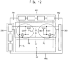
- FIG. 12 is a block diagram view schematically showing a display apparatus according to an example embodiment.
- the display apparatus includes a display panel 100 A, a gate driver circuit 200 , a second level switch 300 , and a data driver circuit 400 .
- the display panel 100 A may be divided into a display area DA and a peripheral area PA surrounding the display area DA.
- a plurality of gate lines, a plurality of data lines, and a plurality of pixel units (e.g., pixels) are disposed in the display area DA.
- the display panel 100 A may further include a plurality of control lines CL, which are adjacent to the gate lines GL and are disposed in parallel with the gate lines GL.
- Each of the pixel units P include a pixel transistor TR, which is electrically coupled (e.g., electrically connected) to a gate line GL and a data line DL, a liquid crystal capacitor CLC, which is electrically coupled to the pixel transistor TR, and a storage capacitor CST, which is electrically coupled to the liquid crystal capacitor CLC.
- a pixel transistor TR which is electrically coupled (e.g., electrically connected) to a gate line GL and a data line DL
- a liquid crystal capacitor CLC which is electrically coupled to the pixel transistor TR
- a storage capacitor CST which is electrically coupled to the liquid crystal capacitor CLC.
- the gate driver circuit 200 is disposed in a first peripheral area PA 1 of the peripheral area PA, which is adjacent to a first end portion of the gate line GL.
- the gate driver circuit 200 is substantially the same as that described in the previous example embodiment referring to FIGS. 2 and 3 .
- the gate driver circuit 200 is configured to generate a plurality of gate signals G 1 , . . . , GM, and to output the gate signals G 1 , . . . , GM to the gate lines GL.
- the gate driver circuit 200 includes a first level switch 203 , which is configured to generate a plurality of first storage signals ST 1 , . . . , STM, and to output the first storage signals ST 1 , . . . , STM to the storage lines STL.
- Each of the storage signals ST 1 , . . . , STM is synchronized with each of the gate signals G 1 , . . . , GM, and has a phase opposite to each of the gate signals G 1 , . . . , GM.
- the storage signal has a first storage low voltage during a period in which the gate signal has a gate on voltage, and has a storage high voltage during a period in which the gate signal has a gate off voltage.
- a first swing voltage ⁇ V 1 between the first storage low voltage and the storage high voltage may compensate for a pixel voltage of a first pixel unit P 1 dropped by a first kickback voltage ⁇ Vkb 1 of the first pixel unit P 1 adjacent to the gate driver circuit 200 .
- the storage high voltage may be substantially the same as the common voltage Vcom of the LC capacitor CLC.
- the gate driver circuit 200 is coupled (e.g., connected) to the control lines CL in the display panel 100 A, and is configured to output the opposite gate signals, which have a phase opposite to that of the gate signals, to the control lines CL.
- the second level switch 300 is located (e.g., directly integrated) in a second peripheral area PA 2 of the peripheral area PA adjacent to a second end portion of the gate line.
- the second level switch 300 is configured to generate a plurality of second storage signals using the gate signals and the opposite gate signals, and to output the second storage signals to the storage lines STL.
- Each of the storage signals ST 1 , . . . , STM is synchronized with each of the gate signals, and has a phase opposite to that of its corresponding one of the gate signals.
- the storage signal has a second storage low voltage during a period in which the gate signal has a gate on voltage, and has a storage high voltage during a period in which the gate signal has a gate off voltage.
- a second swing voltage ⁇ V 2 between the second storage low voltage and the storage high voltage may compensate for a pixel voltage of a second pixel unit P 2 dropped by a second kickback voltage ⁇ Vkb 2 of the second pixel unit P 2 , which is far away from to the gate driver circuit 200 and is adjacent to the second level switch 300 .
- the second storage low voltage is greater than the first storage low voltage.
- a level of the gate signal applied to the second pixel unit P 2 which is far away from the gate driver circuit 200 , is less than a level of the gate signal applied to the first pixel unit P 1 , which is adjacent to the gate driver circuit 200 , by the RC delay of the gate signal.
- the second kickback voltage ⁇ Vkb 2 of the second pixel unit P 2 is less than the first kickback voltage ⁇ Vkb 1 of the first pixel unit P 1 .
- the second swing voltage ⁇ V 2 corresponding to the second kickback voltage ⁇ Vkb 2 is less than the first swing voltage ⁇ V 1 corresponding to the first kickback voltage ⁇ Vkb 1 , and thus, the second storage low voltage is greater than the first storage low voltage.
- the same storage high voltage is applied to the first pixel unit P 1 and the second pixel unit P 2 , and thus, a current path may not be formed between the first pixel unit P 1 and the second pixel unit P 2 .
- the data driver circuit 400 may be disposed on the peripheral area, such as the TCP, and is coupled to the data lines DL.
- the data driver circuit 400 is configured to output the data signals to the data lines.
- the first pixel unit adjacent to the gate driver circuit 200 may be compensated for the kickback voltage by the first level switch 203 in the gate driver circuit 200
- the second pixel unit far away from the gate driver circuit 200 may be compensated for the kickback voltage by the second level switch 300 , and thus, difference kickback voltages according to the RC delay of the gate signal may be easily compensated.
- FIG. 13 is conceptual diagram illustrating first and second level switches shown in FIG. 12 .
- the gate driver circuit 200 is substantially the same as that described in the previous example embodiment referring to FIGS. 2 and 3 .
- the gate driver circuit 200 includes a level shifter 202 and a first level switch 203 as shown in FIGS. 2 and 3 .
- the level shifter 202 is configured to generate a plurality of gate signals based on the gate clock signal CPV.
- the level shifter 202 is configured to generate a plurality of opposite gate signals having a phase opposite to that of the gate signals.
- the level switch 203 includes a first switch SW 1 and a second switch SW 2 .
- the level switch 203 is configured to generate a plurality of storage signals based on the gate signals and the opposite gate signals received from the level shifter 202 , and to output a plurality of storage signals to a plurality of storage lines.
- the first switch SW 1 outputs a first storage low voltage VSTL 1 of a low level, in response to a gate on voltage of a first gate signal G 1 and a gate off voltage of a first opposite gate signal GB 1 having a phase opposite to that of the gate on voltage of the first gate signal G 1 , to a first storage line STL 1 .
- the second switch SW 2 outputs a storage high voltage VSTH of a high level, in response to the gate on voltage of the first opposite gate signal GB 1 and the gate off voltage of the first gate signal G 1 , to the first storage line STL 1 .
- a first storage capacitor CST 1 of the first pixel unit P 1 adjacent to the gate driver circuit 200 receives a ( 1 - 1 )-th storage signal having the first storage low voltage VSTL 1 and the storage high voltage VSTH.
- the second level switch 300 includes a third switch SW 3 and a fourth switch SW 4 .
- the third switch SW 3 includes a fifteenth transistor Q 15 .
- the fifteenth transistor Q 15 includes a control electrode, which is coupled to the first gate line GL 1 , an input electrode, which receives a second storage low voltage VSTL 2 , and an output electrode, which is coupled to the first storage line STL 1 .
- the third switch SW 3 turns on in response to the gate on voltage of the first gate signal G 1 applied to the first gate line GL 1 , and thus, the second storage low voltage VSTL 2 is applied to the first storage line STL 1 .
- the fourth switch SW 4 includes a sixteenth transistor Q 16 .
- the sixteenth transistor Q 16 includes a control electrode, which is coupled to a first control line CL 1 , an input electrode, which receives the storage high voltage VSTH, and an output electrode, which is coupled to the first storage line STL 1 .
- the fourth switch SW 4 turns on in response to the gate on voltage of the first opposite gate signal GB 1 applied to the first control line CL 1 , and thus, the storage high voltage VSTH is applied to the first storage line STL 1 .
- a second storage capacitor CST 2 of the second pixel unit P 2 far away from the gate driver circuit 200 , receives a ( 1 - 2 )-th storage signal having the second storage low voltage VSTL 2 and the storage high voltage VSTH from the second level switch 300 .
- FIG. 14 is a waveform diagram showing signals for driving first and second pixel units by the gate driver circuit and the first and second level switches shown in FIG. 13 .
- the gate driver circuit 200 outputs a first gate signal G 1 to a first gate line GL 1 during a first period T 1 of a frame period.
- the gate driver circuit 200 outputs a ( 1 - 1 )-th storage signal ST 1 - 1 having the first storage low voltage VSTL 1 and the storage high voltage VSTH during the first period T 1 .
- a first LC capacitor CLC 1 of the first pixel unit P 1 which is adjacent to the gate driver circuit 200 , charges a first pixel voltage VP 1 corresponding to a data voltage +Vdata in response to the first gate signal G 1 , and a first storage capacitor CST 1 of the first pixel unit P 1 maintains the first pixel voltage VP 1 charged in the first LC capacitor CLC 1 during the frame period.
- the first pixel voltage VP 1 corresponding to the data voltage +Vdata is maintained during a first period t 1 during which the first gate signal G 1 has the gate on voltage VON. Then, the first pixel voltage VP 1 decreases by a first kickback voltage ⁇ Vkb 1 at a falling timing when the first gate signal G 1 drops from the gate on voltage VON to the gate off voltage VOFF.
- the first storage capacitor CST 1 receives the data voltage +Vdata and the first storage low voltage VSTL 1 .
- the first storage capacitor CST 1 maintains the first pixel voltage VP 1 corresponding to the data voltage +Vdata.
- the first storage capacitor CST 1 receives the storage high voltage VSTH that is greater than the first storage low voltage VSTL 1 .
- the first storage capacitor CST 1 has a voltage increased by a first swing voltage ⁇ V 1 between the first storage low voltage VSTL 1 and the storage high voltage VSTH.
- the increased voltage by the first swing voltage ⁇ V 1 is applied to the first LC capacitor CLC 1 , which is coupled to the first storage capacitor CST 1 , and thus, the first pixel voltage VP 1 decreased by the first kickback voltage ⁇ Vkb 1 may be compensated by the first swing voltage ⁇ V 1 .
- the first level switch 300 outputs a ( 1 - 2 )-th storage signal ST 1 - 2 having to the second storage low voltage VSTL 2 and the storage high voltage VSTH during the first period T 1 .
- a second LC capacitor CLC 2 of the second pixel unit P 2 which is far away from the gate driver circuit 200 , charges a second pixel voltage VP 2 corresponding to a data voltage +Vdata in response to a delayed first gate signal G 1 _ d , and a second storage capacitor CST 2 of the second pixel unit P 2 maintains the second pixel voltage VP 2 charged in the second storage capacitor CST 2 during the frame period.
- the second pixel voltage VP 2 corresponding to the data voltage +Vdata is maintained during a first period t 1 during which the delayed first gate signal G 1 _ d has the gate on voltage VON. Then, the second pixel voltage VP 2 decreases by a kickback voltage ⁇ Vkb at a falling timing when the delayed first gate signal G 1 _ d drops from the gate on voltage VON to the gate off voltage VOFF.
- the second kickback voltage ⁇ Vkb 2 of the second pixel unit P 2 is less than the first kickback voltage ⁇ Vkb 1 of the first pixel unit P 1 .
- the second storage capacitor CST 2 receives the data voltage +Vdata and the second storage low voltage VSTL 2 .
- the second storage capacitor CST 2 maintains the second pixel voltage VP 2 corresponding to the data voltage +Vdata.
- the second storage capacitor CST 2 receives the storage high voltage VSTH that is greater than the second storage low voltage VSTL 2 .
- the second storage capacitor CST 2 has a voltage increased by a second swing voltage ⁇ V 2 between the second storage low voltage VSTL 2 and the storage high voltage VSTH.
- the increased voltage by the second swing voltage ⁇ V 2 is applied to the second LC capacitor CLC 2 , which is coupled to the second storage capacitor CST 2 , and thus, the second pixel voltage VP 2 decreased by the second kickback voltage ⁇ Vkb 2 may be compensated by the second swing voltage ⁇ V 2 .
- the first pixel unit P 1 adjacent to the gate driver circuit 200 may be compensated for the kickback voltage by the first level switch 203 in the gate driver circuit 200
- the second pixel unit P 2 far away from the gate driver circuit 200 may be compensated for the kickback voltage by the second level switch 300 , and thus, difference kickback voltages according to the RC delay of the gate signal may be easily compensated.
- FIG. 15 is a block diagram view schematically showing a display apparatus according to an example embodiment.
- the display apparatus includes a display panel 100 , a first gate driver circuit 200 - 1 , a second gate driver circuit 200 - 2 , and a data driver circuit 400 .
- the display panel 100 may be divided into a display area DA and a peripheral area PA surrounding the display area DA.
- a plurality of gate lines, a plurality of data lines, and a plurality of pixel units (e.g., pixels) are disposed in the display area DA.
- Each of the pixel units P include a pixel transistor TR, which is electrically coupled (e.g., electrically connected) to a gate line GL and a data line DL, a liquid crystal capacitor CLC, which is electrically coupled to the pixel transistor TR, and a storage capacitor CST, which is electrically coupled to the liquid crystal capacitor CLC.
- the first gate driver circuit 200 - 1 is disposed in a first peripheral area PA 1 of the peripheral area, which is adjacent to a first end portion of a gate line GL.
- the first gate driver circuit 200 - 1 is coupled (e.g., connected) to first end portions of the gate lines GL and to first end portions of the storage lines STL.
- the second gate driver circuit 200 - 2 is disposed in a second peripheral area PA 2 of the peripheral area, which is adjacent to a second end portion of the gate line GL.
- the second gate driver circuit 200 - 2 is coupled to second end portions of the gate lines GL and to second end portions of the storage lines STL.
- the first gate driver circuit 200 - 1 is the same or substantially the same as the second gate driver circuit 200 - 2 .
- the first and second gate driver circuits 200 - 1 and 200 - 2 respectively output a same gate signal to a same gate line, and respectively output a same storage signal to a same storage line.
- the display apparatus includes the first and second gate driver circuits 200 - 1 and 200 - 2 , such as a dual gate structure, so that an RC delay difference of the gate signals may be improved.
- the first and second gate driver circuits 200 - 1 and 200 - 2 are substantially the same as that described in the previous example embodiment referring to FIGS. 2 and 3 .
- each of the first and second gate driver circuits 200 - 1 and 200 - 2 is configured to generate a plurality of gate signals G 1 , . . . , GM, and to output the gate signals G 1 , . . . , GM to the gate lines GL.
- each of the first and second gate driver circuits 200 - 1 and 200 - 2 includes a first level switch 203 , which is configured to generate a plurality of first storage signals ST 1 , . . . , STM, and to output the first storage signals ST 1 , . . . , STM to the storage lines STL.
- Each of the storage signals ST 1 , . . . , STM is synchronized with each of the gate signals G 1 , . . . , GM, and has a phase opposite to that of its corresponding one of the gate signals G 1 , . . . , GM.
- the storage signal has a first storage low voltage during a period in which the gate signal has a gate on voltage, and has a storage high voltage during a period in which the gate signal has a gate off voltage.
- a swing voltage between the storage low voltage and the storage high voltage may compensate for a pixel voltage dropped by a kickback voltage of the pixel unit P.
- One of the storage low voltage and the storage high voltage may be substantially the same as the common voltage Vcom of the LC capacitor CLC.
- the data driver circuit 400 may be disposed on the peripheral area, such as the TCP, and is coupled to the data lines DL.
- the data driver circuit 400 is configured to output the data signals to the data lines.
- both end portions of the gate line receives the gate signal without the RC delay from the first and second gate driver circuits, such as the dual gate structure.
- the pixel units which are adjacent to both end portions of the gate line, have a same kickback voltage, and the same kickback voltage may be compensated using the swing voltage between the storage low voltage and the storage high voltage.
- FIG. 16 is a waveform diagram illustrating a method of compensating a kickback voltage according to an example embodiment.
- a display apparatus includes a storage capacitor that receives a DC signal as the storage signal.
- the display apparatus includes a storage capacitor that receives the storage signal having a storage low voltage and a storage high voltage in synchronization with the gate signal.
- a pixel voltage VP charged in an LC capacitor is decreased by a kickback voltage ⁇ Vkb during a falling timing of the gate signal G.
- the kickback voltage ⁇ Vkb is changed according to an LC capacitance corresponding to a grayscale level, and thus, the pixel voltage VP is changed. Therefore, according to the comparative example embodiment, the kickback voltage is changed according to the data voltage applied to the LC capacitor, and thus, is difficult to be compensated.
- the kickback voltage is compensated using the storage signal having a multi-level, so that the pixel voltage VP charged in the LC capacitor may be maintained to a target pixel voltage.
- the kickback voltage may be compensated without reference to the LC capacitance, that is, the data voltage applied to the LC capacitor.
- the storage signal for the storage capacitor includes a multi-level signal swing between a low voltage and a high voltage in synchronization with the gate signal, and thus, the kickback voltage may be compensated without reference to a change of the LC capacitance.
Landscapes
- Engineering & Computer Science (AREA)
- Physics & Mathematics (AREA)
- General Physics & Mathematics (AREA)
- Crystallography & Structural Chemistry (AREA)
- Chemical & Material Sciences (AREA)
- Theoretical Computer Science (AREA)
- Computer Hardware Design (AREA)
- Control Of Indicators Other Than Cathode Ray Tubes (AREA)
- Liquid Crystal Display Device Control (AREA)
- Nonlinear Science (AREA)
- Mathematical Physics (AREA)
- Optics & Photonics (AREA)
- Multimedia (AREA)
- Microelectronics & Electronic Packaging (AREA)
- Liquid Crystal (AREA)
Abstract
Description
Claims (18)
Applications Claiming Priority (2)
| Application Number | Priority Date | Filing Date | Title |
|---|---|---|---|
| KR1020140107004A KR20160021942A (en) | 2014-08-18 | 2014-08-18 | Display apparatus and method of driving the display apparatus |
| KR10-2014-0107004 | 2014-08-18 |
Publications (2)
| Publication Number | Publication Date |
|---|---|
| US20160049136A1 US20160049136A1 (en) | 2016-02-18 |
| US10553166B2 true US10553166B2 (en) | 2020-02-04 |
Family
ID=55302616
Family Applications (1)
| Application Number | Title | Priority Date | Filing Date |
|---|---|---|---|
| US14/671,982 Expired - Fee Related US10553166B2 (en) | 2014-08-18 | 2015-03-27 | Display apparatus and method of driving the display apparatus |
Country Status (3)
| Country | Link |
|---|---|
| US (1) | US10553166B2 (en) |
| KR (1) | KR20160021942A (en) |
| CN (1) | CN105374326B (en) |
Cited By (3)
| Publication number | Priority date | Publication date | Assignee | Title |
|---|---|---|---|---|
| US11232734B2 (en) * | 2019-09-25 | 2022-01-25 | Boe Technology Group Co., Ltd. | Shift register unit, driving method, gate driving circuit and display device |
| US20220335878A1 (en) * | 2021-04-14 | 2022-10-20 | Samsung Display Co., Ltd. | Gate driver and display device including the same |
| US20220366837A1 (en) * | 2020-12-04 | 2022-11-17 | Xiamen Tianma Micro-Electronics Co., Ltd. | Display panel, detection method thereof and display device |
Families Citing this family (7)
| Publication number | Priority date | Publication date | Assignee | Title |
|---|---|---|---|---|
| KR102477916B1 (en) * | 2015-10-15 | 2022-12-15 | 삼성디스플레이 주식회사 | Liquid display device |
| CN105206238B (en) * | 2015-10-15 | 2017-12-15 | 武汉华星光电技术有限公司 | The display device of gate driving circuit and the application circuit |
| TWI625578B (en) * | 2017-05-17 | 2018-06-01 | 友達光電股份有限公司 | Display panel and its pixel circuit |
| CN107578741B (en) * | 2017-09-28 | 2020-03-27 | 京东方科技集团股份有限公司 | Shifting register unit and driving method thereof, grid driving circuit and display device |
| CN107945764B (en) * | 2018-01-08 | 2020-06-09 | 惠科股份有限公司 | Driving circuit of display panel, display device and driving method of display panel |
| KR102668997B1 (en) * | 2019-10-21 | 2024-05-24 | 삼성디스플레이 주식회사 | Display device |
| KR20240133415A (en) * | 2023-02-28 | 2024-09-04 | 엘지디스플레이 주식회사 | Display panel and display device |
Citations (51)
| Publication number | Priority date | Publication date | Assignee | Title |
|---|---|---|---|---|
| US4621260A (en) * | 1982-12-25 | 1986-11-04 | Tokyo Shibaura Denki Kabushiki Kaisha | Thin-film transistor circuit |
| US5777515A (en) * | 1995-05-11 | 1998-07-07 | Matsushita Electric Industrial Co., Ltd. | Operational amplifier apparatus |
| US5784039A (en) * | 1993-06-25 | 1998-07-21 | Hosiden Corporation | Liquid crystal display AC-drive method and liquid crystal display using the same |
| US6052103A (en) * | 1996-09-30 | 2000-04-18 | Kabushiki Kaisha Toshiba | Liquid-crystal display device and driving method thereof |
| US6115018A (en) * | 1996-03-26 | 2000-09-05 | Kabushiki Kaisha Toshiba | Active matrix liquid crystal display device |
| US6177965B1 (en) * | 1993-04-22 | 2001-01-23 | Matsushita Electric Industrial Co., Ltd. | Display device and projection-type display apparatus using the device |
| US6246385B1 (en) * | 1997-04-28 | 2001-06-12 | Matsushita Electric Industrial Co., Ltd. | Liquid crystal display device and its driving method |
| US6590552B1 (en) * | 1998-06-29 | 2003-07-08 | Sanyo Electric Co., Ltd. | Method of driving liquid crystal display device |
| US6680720B1 (en) * | 1999-01-11 | 2004-01-20 | Lg. Phillips Lcd Co., Ltd. | Apparatus for driving liquid crystal display |
| US20040189884A1 (en) * | 2003-03-31 | 2004-09-30 | Kim Cheon Hong | Liquid crystal display |
| US7027024B2 (en) * | 1998-03-27 | 2006-04-11 | Sharp Kabushiki Kaisha | Display device and display method |
| US20060145978A1 (en) * | 2004-12-15 | 2006-07-06 | Nec Corporation | Liquid crystal display apparatus, driving method for same, and driving circuit for same |
| US20060145985A1 (en) * | 2004-12-31 | 2006-07-06 | Hwang Han W | Liquid crystal display device and driving method thereof |
| US20060231838A1 (en) * | 2005-04-13 | 2006-10-19 | Samsung Electronics Co., Ltd. | Liquid crystal display |
| US20070262938A1 (en) * | 2006-05-10 | 2007-11-15 | Cheol Se Kim | Liquid crystal display panel, liquid crystal display device having the same, and driving method thereof |
| US20070296682A1 (en) * | 2006-06-22 | 2007-12-27 | Samsung Electronics Co., Ltd. | Liquid crystal display device and driving method thereof |
| CN101118357A (en) | 2006-08-01 | 2008-02-06 | 三星电子株式会社 | display device |
| US20080094314A1 (en) * | 2004-09-17 | 2008-04-24 | Koninklijke Philips Electronics, N.V. | Display Unit |
| KR20080043097A (en) | 2006-11-13 | 2008-05-16 | 삼성전자주식회사 | Display device |
| KR20080054549A (en) | 2006-12-13 | 2008-06-18 | 삼성전자주식회사 | Liquid crystal display |
| US20090128527A1 (en) * | 2007-08-30 | 2009-05-21 | Sony Corporation | Display apparatus, driving method of the same and electronic equipment using the same |
| US20090147164A1 (en) * | 2007-08-30 | 2009-06-11 | Sony Corporation | Display apparatus and electronic equipment |
| US20090189677A1 (en) * | 2008-01-25 | 2009-07-30 | Samsung Electronics Co., Ltd | Gate driving circuit and display apparatus having the same |
| US20090231504A1 (en) * | 2008-03-14 | 2009-09-17 | Epson Imaging Devices Corporation | Liquid crystal display device |
| US20100045884A1 (en) * | 2008-08-25 | 2010-02-25 | Soon-Il Ahn | Liquid Crystal Display |
| US20100073354A1 (en) * | 2008-09-22 | 2010-03-25 | Samsung Electronics Co., Ltd. | Panel assembly and display apparatus having the same |
| US20100245328A1 (en) * | 2007-12-28 | 2010-09-30 | Yasushi Sasaki | Storage capacitor line drive circuit and display device |
| US20110001743A1 (en) * | 2008-03-11 | 2011-01-06 | Asahi Yamato | Drive circuit, drive method, liquid crystal display panel, liquid crystal module, and liquid cystal display device |
| US7936332B2 (en) * | 2006-06-21 | 2011-05-03 | Samsung Electronics Co., Ltd. | Gate driving circuit having reduced ripple effect and display apparatus having the same |
| CN102222456A (en) | 2010-04-16 | 2011-10-19 | 北京京东方光电科技有限公司 | Common electrode driving method, circuit and liquid crystal displayer |
| US20110273416A1 (en) * | 2010-05-06 | 2011-11-10 | Samsung Electronics Co., Ltd. | Voltage generating circuit and display apparatus having the same |
| US8059780B2 (en) * | 2010-03-19 | 2011-11-15 | Au Optronics Corp. | Shift register circuit and gate driving circuit |
| US20120139883A1 (en) * | 2010-12-02 | 2012-06-07 | Jae-Hoon Lee | Gate drive circuit and display apparatus having the same |
| US20120169690A1 (en) * | 2009-09-16 | 2012-07-05 | Sharp Kabushiki Kaisha | Display device and drive method for display device |
| US20120200614A1 (en) * | 2009-10-16 | 2012-08-09 | Sharp Kabushiki Kaisha | Display driving circuit, display device, and display driving method |
| US8264250B2 (en) * | 2004-10-25 | 2012-09-11 | Samsung Electronics Co., Ltd. | Array substrate having increased inspection efficiency and display apparatus having the same |
| US20120229523A1 (en) * | 2011-03-10 | 2012-09-13 | Panasonic Liquid Crystal Display Co., Ltd. | Liquid crystal display device |
| US20130009924A1 (en) * | 2010-04-02 | 2013-01-10 | Sharp Kabushiki Kaisha | Display device and method of driving the same |
| US20130093658A1 (en) * | 2011-10-14 | 2013-04-18 | Samsung Display Co., Ltd. | Display device |
| KR20130072909A (en) | 2011-12-22 | 2013-07-02 | 엘지디스플레이 주식회사 | Shift register and display device including the same |
| US20130249882A1 (en) * | 2012-03-26 | 2013-09-26 | Shenzhen China Star Optoelectronics Technology, Co., Ltd. | Liquid Crystal Display Device and Driving Method |
| US9052538B2 (en) * | 2012-04-25 | 2015-06-09 | Lg Display Co., Ltd. | Liquid crystal display device |
| US20150185531A1 (en) * | 2013-12-31 | 2015-07-02 | Shenzhen China Star Optoelectronics Technology Co Ltd. | Liquid crystal display panel, pixel structure and driving method thereof |
| US20150235590A1 (en) * | 2014-02-17 | 2015-08-20 | Au Optronics (Xiamen) Corporation | Display panel and gate driver |
| US9148148B2 (en) * | 2010-10-28 | 2015-09-29 | Samsung Display Co., Ltd. | Gate driving circuit and display apparatus having the same |
| US9280953B2 (en) * | 2014-03-21 | 2016-03-08 | Chunghwa Picture Tubes, Ltd. | Display panel |
| US20160133216A1 (en) * | 2014-11-07 | 2016-05-12 | Samsung Display Co., Ltd. | Display apparatus |
| US9378710B2 (en) * | 2010-10-29 | 2016-06-28 | Japan Display Inc. | Display device |
| US20160240158A1 (en) * | 2014-01-27 | 2016-08-18 | Shenzhen China Star Optoelectronics Technology Co., Ltd. | Goa unit for co-driving gate and common electrodes, drive circuit and array |
| US20170084247A1 (en) * | 2015-09-21 | 2017-03-23 | Apple Inc. | Gate line layout configuration |
| US10078987B2 (en) * | 2015-11-27 | 2018-09-18 | Samsung Display Co., Ltd. | Display apparatus |
-
2014
- 2014-08-18 KR KR1020140107004A patent/KR20160021942A/en not_active Ceased
-
2015
- 2015-03-27 US US14/671,982 patent/US10553166B2/en not_active Expired - Fee Related
- 2015-08-07 CN CN201510484980.1A patent/CN105374326B/en not_active Expired - Fee Related
Patent Citations (59)
| Publication number | Priority date | Publication date | Assignee | Title |
|---|---|---|---|---|
| US4621260A (en) * | 1982-12-25 | 1986-11-04 | Tokyo Shibaura Denki Kabushiki Kaisha | Thin-film transistor circuit |
| US6177965B1 (en) * | 1993-04-22 | 2001-01-23 | Matsushita Electric Industrial Co., Ltd. | Display device and projection-type display apparatus using the device |
| US5784039A (en) * | 1993-06-25 | 1998-07-21 | Hosiden Corporation | Liquid crystal display AC-drive method and liquid crystal display using the same |
| US5777515A (en) * | 1995-05-11 | 1998-07-07 | Matsushita Electric Industrial Co., Ltd. | Operational amplifier apparatus |
| US6115018A (en) * | 1996-03-26 | 2000-09-05 | Kabushiki Kaisha Toshiba | Active matrix liquid crystal display device |
| US6052103A (en) * | 1996-09-30 | 2000-04-18 | Kabushiki Kaisha Toshiba | Liquid-crystal display device and driving method thereof |
| US6246385B1 (en) * | 1997-04-28 | 2001-06-12 | Matsushita Electric Industrial Co., Ltd. | Liquid crystal display device and its driving method |
| US7027024B2 (en) * | 1998-03-27 | 2006-04-11 | Sharp Kabushiki Kaisha | Display device and display method |
| US6590552B1 (en) * | 1998-06-29 | 2003-07-08 | Sanyo Electric Co., Ltd. | Method of driving liquid crystal display device |
| US6680720B1 (en) * | 1999-01-11 | 2004-01-20 | Lg. Phillips Lcd Co., Ltd. | Apparatus for driving liquid crystal display |
| US20040189884A1 (en) * | 2003-03-31 | 2004-09-30 | Kim Cheon Hong | Liquid crystal display |
| US20080094314A1 (en) * | 2004-09-17 | 2008-04-24 | Koninklijke Philips Electronics, N.V. | Display Unit |
| US8264250B2 (en) * | 2004-10-25 | 2012-09-11 | Samsung Electronics Co., Ltd. | Array substrate having increased inspection efficiency and display apparatus having the same |
| US20060145978A1 (en) * | 2004-12-15 | 2006-07-06 | Nec Corporation | Liquid crystal display apparatus, driving method for same, and driving circuit for same |
| US20060145985A1 (en) * | 2004-12-31 | 2006-07-06 | Hwang Han W | Liquid crystal display device and driving method thereof |
| US20060231838A1 (en) * | 2005-04-13 | 2006-10-19 | Samsung Electronics Co., Ltd. | Liquid crystal display |
| US7969396B2 (en) | 2005-04-13 | 2011-06-28 | Samsung Electronics Co., Ltd. | Liquid crystal display |
| US20070262938A1 (en) * | 2006-05-10 | 2007-11-15 | Cheol Se Kim | Liquid crystal display panel, liquid crystal display device having the same, and driving method thereof |
| US7936332B2 (en) * | 2006-06-21 | 2011-05-03 | Samsung Electronics Co., Ltd. | Gate driving circuit having reduced ripple effect and display apparatus having the same |
| US20070296682A1 (en) * | 2006-06-22 | 2007-12-27 | Samsung Electronics Co., Ltd. | Liquid crystal display device and driving method thereof |
| CN101118357A (en) | 2006-08-01 | 2008-02-06 | 三星电子株式会社 | display device |
| US8063860B2 (en) | 2006-08-01 | 2011-11-22 | Samsung Electronics Co., Ltd. | Display device |
| KR20080043097A (en) | 2006-11-13 | 2008-05-16 | 삼성전자주식회사 | Display device |
| KR20080054549A (en) | 2006-12-13 | 2008-06-18 | 삼성전자주식회사 | Liquid crystal display |
| US20090128527A1 (en) * | 2007-08-30 | 2009-05-21 | Sony Corporation | Display apparatus, driving method of the same and electronic equipment using the same |
| US20090147164A1 (en) * | 2007-08-30 | 2009-06-11 | Sony Corporation | Display apparatus and electronic equipment |
| CN101965607A (en) | 2007-12-28 | 2011-02-02 | 夏普株式会社 | Auxiliary capacitor wiring drive circuit and display device |
| US8587572B2 (en) | 2007-12-28 | 2013-11-19 | Sharp Kabushiki Kaisha | Storage capacitor line drive circuit and display device |
| US20100245328A1 (en) * | 2007-12-28 | 2010-09-30 | Yasushi Sasaki | Storage capacitor line drive circuit and display device |
| US20090189677A1 (en) * | 2008-01-25 | 2009-07-30 | Samsung Electronics Co., Ltd | Gate driving circuit and display apparatus having the same |
| US20110001743A1 (en) * | 2008-03-11 | 2011-01-06 | Asahi Yamato | Drive circuit, drive method, liquid crystal display panel, liquid crystal module, and liquid cystal display device |
| JP2009222839A (en) | 2008-03-14 | 2009-10-01 | Epson Imaging Devices Corp | Liquid crystal display device |
| US20090231504A1 (en) * | 2008-03-14 | 2009-09-17 | Epson Imaging Devices Corporation | Liquid crystal display device |
| US8199087B2 (en) | 2008-03-14 | 2012-06-12 | Epson Imaging Devices Corporation | Liquid crystal display device |
| US20100045884A1 (en) * | 2008-08-25 | 2010-02-25 | Soon-Il Ahn | Liquid Crystal Display |
| US20100073354A1 (en) * | 2008-09-22 | 2010-03-25 | Samsung Electronics Co., Ltd. | Panel assembly and display apparatus having the same |
| US20120169690A1 (en) * | 2009-09-16 | 2012-07-05 | Sharp Kabushiki Kaisha | Display device and drive method for display device |
| US20120200614A1 (en) * | 2009-10-16 | 2012-08-09 | Sharp Kabushiki Kaisha | Display driving circuit, display device, and display driving method |
| US8059780B2 (en) * | 2010-03-19 | 2011-11-15 | Au Optronics Corp. | Shift register circuit and gate driving circuit |
| US20130009924A1 (en) * | 2010-04-02 | 2013-01-10 | Sharp Kabushiki Kaisha | Display device and method of driving the same |
| CN102222456A (en) | 2010-04-16 | 2011-10-19 | 北京京东方光电科技有限公司 | Common electrode driving method, circuit and liquid crystal displayer |
| US20120092312A1 (en) * | 2010-04-16 | 2012-04-19 | Beijing Boe Optoelectronics Technology Co., Ltd. | Driving method for common electrodes, circuit and liquid crystal display thereof |
| US8896583B2 (en) | 2010-04-16 | 2014-11-25 | Beijing Boe Optoelectronics Technology Co., Ltd. | Common electrode driving method, common electrode driving circuit and liquid crystal display |
| US20110273416A1 (en) * | 2010-05-06 | 2011-11-10 | Samsung Electronics Co., Ltd. | Voltage generating circuit and display apparatus having the same |
| US9148148B2 (en) * | 2010-10-28 | 2015-09-29 | Samsung Display Co., Ltd. | Gate driving circuit and display apparatus having the same |
| US9378710B2 (en) * | 2010-10-29 | 2016-06-28 | Japan Display Inc. | Display device |
| US20120139883A1 (en) * | 2010-12-02 | 2012-06-07 | Jae-Hoon Lee | Gate drive circuit and display apparatus having the same |
| US20120229523A1 (en) * | 2011-03-10 | 2012-09-13 | Panasonic Liquid Crystal Display Co., Ltd. | Liquid crystal display device |
| US20130093658A1 (en) * | 2011-10-14 | 2013-04-18 | Samsung Display Co., Ltd. | Display device |
| KR20130072909A (en) | 2011-12-22 | 2013-07-02 | 엘지디스플레이 주식회사 | Shift register and display device including the same |
| US20130249882A1 (en) * | 2012-03-26 | 2013-09-26 | Shenzhen China Star Optoelectronics Technology, Co., Ltd. | Liquid Crystal Display Device and Driving Method |
| US9052538B2 (en) * | 2012-04-25 | 2015-06-09 | Lg Display Co., Ltd. | Liquid crystal display device |
| US20150185531A1 (en) * | 2013-12-31 | 2015-07-02 | Shenzhen China Star Optoelectronics Technology Co Ltd. | Liquid crystal display panel, pixel structure and driving method thereof |
| US20160240158A1 (en) * | 2014-01-27 | 2016-08-18 | Shenzhen China Star Optoelectronics Technology Co., Ltd. | Goa unit for co-driving gate and common electrodes, drive circuit and array |
| US20150235590A1 (en) * | 2014-02-17 | 2015-08-20 | Au Optronics (Xiamen) Corporation | Display panel and gate driver |
| US9280953B2 (en) * | 2014-03-21 | 2016-03-08 | Chunghwa Picture Tubes, Ltd. | Display panel |
| US20160133216A1 (en) * | 2014-11-07 | 2016-05-12 | Samsung Display Co., Ltd. | Display apparatus |
| US20170084247A1 (en) * | 2015-09-21 | 2017-03-23 | Apple Inc. | Gate line layout configuration |
| US10078987B2 (en) * | 2015-11-27 | 2018-09-18 | Samsung Display Co., Ltd. | Display apparatus |
Cited By (5)
| Publication number | Priority date | Publication date | Assignee | Title |
|---|---|---|---|---|
| US11232734B2 (en) * | 2019-09-25 | 2022-01-25 | Boe Technology Group Co., Ltd. | Shift register unit, driving method, gate driving circuit and display device |
| US20220366837A1 (en) * | 2020-12-04 | 2022-11-17 | Xiamen Tianma Micro-Electronics Co., Ltd. | Display panel, detection method thereof and display device |
| US11749179B2 (en) * | 2020-12-04 | 2023-09-05 | Xiamen Tianma Micro-Electronics Co., Ltd. | Display panel, detection method thereof and display device |
| US20220335878A1 (en) * | 2021-04-14 | 2022-10-20 | Samsung Display Co., Ltd. | Gate driver and display device including the same |
| US11756477B2 (en) * | 2021-04-14 | 2023-09-12 | Samsung Display Co., Ltd. | Gate driver and display device including the same |
Also Published As
| Publication number | Publication date |
|---|---|
| CN105374326B (en) | 2020-03-13 |
| US20160049136A1 (en) | 2016-02-18 |
| CN105374326A (en) | 2016-03-02 |
| KR20160021942A (en) | 2016-02-29 |
Similar Documents
| Publication | Publication Date | Title |
|---|---|---|
| US10553166B2 (en) | Display apparatus and method of driving the display apparatus | |
| KR101543281B1 (en) | Gate drive circuit and display device having the same | |
| US7310402B2 (en) | Gate line drivers for active matrix displays | |
| US8552958B2 (en) | Method of driving a gate line, gate drive circuit for performing the method and display apparatus having the gate drive circuit | |
| US9293093B2 (en) | Gate driver in which each stage thereof drives multiple gate lines and display apparatus having the same | |
| US8456409B2 (en) | Gate drive circuit and display apparatus having the same | |
| US8194026B2 (en) | Gate driver and display apparatus having the same | |
| EP2043083B1 (en) | Liquid crystal display | |
| US8810498B2 (en) | Gate driving circuit and display apparatus having the same | |
| US8754674B2 (en) | Gate drive circuit and method of driving the same | |
| US9047803B2 (en) | Display apparatus including bi-directional gate drive circuit | |
| US8284149B2 (en) | Gate driving circuit and display device having the gate driving circuit | |
| EP2549483A1 (en) | Shift register | |
| US8422622B2 (en) | Shift register and display device | |
| US7880503B2 (en) | Method of driving gate lines, gate line drive circuit for performing the method and display device having the gate line drive circuit | |
| US20100177082A1 (en) | Gate driving circuit and display apparatus having the same | |
| US8619070B2 (en) | Gate drive circuit and display apparatus having the same | |
| KR20100075141A (en) | Gate driving circuit and display device having the gate driving circuit | |
| KR101428713B1 (en) | Gate driving circuit and liquid crystal display device using the same | |
| KR20110102627A (en) | Shift register and display device using it | |
| US20080278214A1 (en) | Method for removing noise, switching circuit for performing the same and display device having the switching circuit | |
| WO2013018596A1 (en) | Method for powering lcd device and auxiliary capacity line | |
| KR20120060298A (en) | Gate driving circuit and display device having the same | |
| KR101860732B1 (en) | Gate driving circuit and display device having the same | |
| US8547319B2 (en) | Display apparatus including a gate driver that has a plurality of stages and method for driving the display apparatus |
Legal Events
| Date | Code | Title | Description |
|---|---|---|---|
| AS | Assignment |
Owner name: SAMSUNG DISPLAY CO., LTD., KOREA, REPUBLIC OF Free format text: ASSIGNMENT OF ASSIGNORS INTEREST;ASSIGNORS:SEO, JI-MYOUNG;PARK, SU-HYEONG;YOON, SOO-WAN;AND OTHERS;SIGNING DATES FROM 20150124 TO 20150128;REEL/FRAME:035872/0091 |
|
| STPP | Information on status: patent application and granting procedure in general |
Free format text: RESPONSE TO NON-FINAL OFFICE ACTION ENTERED AND FORWARDED TO EXAMINER |
|
| STPP | Information on status: patent application and granting procedure in general |
Free format text: FINAL REJECTION MAILED |
|
| STPP | Information on status: patent application and granting procedure in general |
Free format text: RESPONSE AFTER FINAL ACTION FORWARDED TO EXAMINER |
|
| STPP | Information on status: patent application and granting procedure in general |
Free format text: NOTICE OF ALLOWANCE MAILED -- APPLICATION RECEIVED IN OFFICE OF PUBLICATIONS |
|
| ZAAA | Notice of allowance and fees due |
Free format text: ORIGINAL CODE: NOA |
|
| ZAAB | Notice of allowance mailed |
Free format text: ORIGINAL CODE: MN/=. |
|
| STPP | Information on status: patent application and granting procedure in general |
Free format text: PUBLICATIONS -- ISSUE FEE PAYMENT VERIFIED |
|
| STCF | Information on status: patent grant |
Free format text: PATENTED CASE |
|
| FEPP | Fee payment procedure |
Free format text: MAINTENANCE FEE REMINDER MAILED (ORIGINAL EVENT CODE: REM.); ENTITY STATUS OF PATENT OWNER: LARGE ENTITY |
|
| LAPS | Lapse for failure to pay maintenance fees |
Free format text: PATENT EXPIRED FOR FAILURE TO PAY MAINTENANCE FEES (ORIGINAL EVENT CODE: EXP.); ENTITY STATUS OF PATENT OWNER: LARGE ENTITY |
|
| STCH | Information on status: patent discontinuation |
Free format text: PATENT EXPIRED DUE TO NONPAYMENT OF MAINTENANCE FEES UNDER 37 CFR 1.362 |
|
| FP | Lapsed due to failure to pay maintenance fee |
Effective date: 20240204 |