US10535779B2 - Thin film transistor and method for manufacturing thin film transistor - Google Patents
Thin film transistor and method for manufacturing thin film transistor Download PDFInfo
- Publication number
- US10535779B2 US10535779B2 US15/872,879 US201815872879A US10535779B2 US 10535779 B2 US10535779 B2 US 10535779B2 US 201815872879 A US201815872879 A US 201815872879A US 10535779 B2 US10535779 B2 US 10535779B2
- Authority
- US
- United States
- Prior art keywords
- layer
- oxide semiconductor
- fluorine
- semiconductor layer
- insulating layer
- Prior art date
- Legal status (The legal status is an assumption and is not a legal conclusion. Google has not performed a legal analysis and makes no representation as to the accuracy of the status listed.)
- Active
Links
Images


Classifications
-
- H01L29/7869—
-
- H—ELECTRICITY
- H10—SEMICONDUCTOR DEVICES; ELECTRIC SOLID-STATE DEVICES NOT OTHERWISE PROVIDED FOR
- H10D—INORGANIC ELECTRIC SEMICONDUCTOR DEVICES
- H10D30/00—Field-effect transistors [FET]
- H10D30/60—Insulated-gate field-effect transistors [IGFET]
- H10D30/67—Thin-film transistors [TFT]
- H10D30/674—Thin-film transistors [TFT] characterised by the active materials
- H10D30/6755—Oxide semiconductors, e.g. zinc oxide, copper aluminium oxide or cadmium stannate
-
- H01L21/385—
-
- H01L21/44—
-
- H01L21/47576—
-
- H01L29/26—
-
- H01L29/4908—
-
- H01L29/66969—
-
- H—ELECTRICITY
- H10—SEMICONDUCTOR DEVICES; ELECTRIC SOLID-STATE DEVICES NOT OTHERWISE PROVIDED FOR
- H10D—INORGANIC ELECTRIC SEMICONDUCTOR DEVICES
- H10D30/00—Field-effect transistors [FET]
- H10D30/60—Insulated-gate field-effect transistors [IGFET]
- H10D30/67—Thin-film transistors [TFT]
- H10D30/6729—Thin-film transistors [TFT] characterised by the electrodes
- H10D30/6737—Thin-film transistors [TFT] characterised by the electrodes characterised by the electrode materials
- H10D30/6739—Conductor-insulator-semiconductor electrodes
-
- H—ELECTRICITY
- H10—SEMICONDUCTOR DEVICES; ELECTRIC SOLID-STATE DEVICES NOT OTHERWISE PROVIDED FOR
- H10D—INORGANIC ELECTRIC SEMICONDUCTOR DEVICES
- H10D30/00—Field-effect transistors [FET]
- H10D30/60—Insulated-gate field-effect transistors [IGFET]
- H10D30/67—Thin-film transistors [TFT]
- H10D30/674—Thin-film transistors [TFT] characterised by the active materials
- H10D30/6755—Oxide semiconductors, e.g. zinc oxide, copper aluminium oxide or cadmium stannate
- H10D30/6756—Amorphous oxide semiconductors
-
- H—ELECTRICITY
- H10—SEMICONDUCTOR DEVICES; ELECTRIC SOLID-STATE DEVICES NOT OTHERWISE PROVIDED FOR
- H10D—INORGANIC ELECTRIC SEMICONDUCTOR DEVICES
- H10D30/00—Field-effect transistors [FET]
- H10D30/60—Insulated-gate field-effect transistors [IGFET]
- H10D30/67—Thin-film transistors [TFT]
- H10D30/6757—Thin-film transistors [TFT] characterised by the structure of the channel, e.g. transverse or longitudinal shape or doping profile
-
- H—ELECTRICITY
- H10—SEMICONDUCTOR DEVICES; ELECTRIC SOLID-STATE DEVICES NOT OTHERWISE PROVIDED FOR
- H10D—INORGANIC ELECTRIC SEMICONDUCTOR DEVICES
- H10D62/00—Semiconductor bodies, or regions thereof, of devices having potential barriers
- H10D62/80—Semiconductor bodies, or regions thereof, of devices having potential barriers characterised by the materials
-
- H—ELECTRICITY
- H10—SEMICONDUCTOR DEVICES; ELECTRIC SOLID-STATE DEVICES NOT OTHERWISE PROVIDED FOR
- H10D—INORGANIC ELECTRIC SEMICONDUCTOR DEVICES
- H10D64/00—Electrodes of devices having potential barriers
- H10D64/01—Manufacture or treatment
- H10D64/011—Manufacture or treatment of electrodes ohmically coupled to a semiconductor
-
- H—ELECTRICITY
- H10—SEMICONDUCTOR DEVICES; ELECTRIC SOLID-STATE DEVICES NOT OTHERWISE PROVIDED FOR
- H10D—INORGANIC ELECTRIC SEMICONDUCTOR DEVICES
- H10D99/00—Subject matter not provided for in other groups of this subclass
-
- H—ELECTRICITY
- H10—SEMICONDUCTOR DEVICES; ELECTRIC SOLID-STATE DEVICES NOT OTHERWISE PROVIDED FOR
- H10P—GENERIC PROCESSES OR APPARATUS FOR THE MANUFACTURE OR TREATMENT OF DEVICES COVERED BY CLASS H10
- H10P14/00—Formation of materials, e.g. in the shape of layers or pillars
- H10P14/20—Formation of materials, e.g. in the shape of layers or pillars of semiconductor materials
- H10P14/22—Formation of materials, e.g. in the shape of layers or pillars of semiconductor materials using physical deposition, e.g. vacuum deposition or sputtering
-
- H—ELECTRICITY
- H10—SEMICONDUCTOR DEVICES; ELECTRIC SOLID-STATE DEVICES NOT OTHERWISE PROVIDED FOR
- H10P—GENERIC PROCESSES OR APPARATUS FOR THE MANUFACTURE OR TREATMENT OF DEVICES COVERED BY CLASS H10
- H10P14/00—Formation of materials, e.g. in the shape of layers or pillars
- H10P14/20—Formation of materials, e.g. in the shape of layers or pillars of semiconductor materials
- H10P14/29—Formation of materials, e.g. in the shape of layers or pillars of semiconductor materials characterised by the substrates
- H10P14/2901—Materials
- H10P14/2922—Materials being non-crystalline insulating materials, e.g. glass or polymers
-
- H—ELECTRICITY
- H10—SEMICONDUCTOR DEVICES; ELECTRIC SOLID-STATE DEVICES NOT OTHERWISE PROVIDED FOR
- H10P—GENERIC PROCESSES OR APPARATUS FOR THE MANUFACTURE OR TREATMENT OF DEVICES COVERED BY CLASS H10
- H10P14/00—Formation of materials, e.g. in the shape of layers or pillars
- H10P14/20—Formation of materials, e.g. in the shape of layers or pillars of semiconductor materials
- H10P14/32—Formation of materials, e.g. in the shape of layers or pillars of semiconductor materials characterised by intermediate layers between substrates and deposited layers
- H10P14/3202—Materials thereof
- H10P14/3238—Materials thereof being insulating materials
-
- H—ELECTRICITY
- H10—SEMICONDUCTOR DEVICES; ELECTRIC SOLID-STATE DEVICES NOT OTHERWISE PROVIDED FOR
- H10P—GENERIC PROCESSES OR APPARATUS FOR THE MANUFACTURE OR TREATMENT OF DEVICES COVERED BY CLASS H10
- H10P14/00—Formation of materials, e.g. in the shape of layers or pillars
- H10P14/20—Formation of materials, e.g. in the shape of layers or pillars of semiconductor materials
- H10P14/34—Deposited materials, e.g. layers
- H10P14/3402—Deposited materials, e.g. layers characterised by the chemical composition
- H10P14/3424—Deposited materials, e.g. layers characterised by the chemical composition being Group IIB-VIA materials
- H10P14/3426—Oxides
-
- H—ELECTRICITY
- H10—SEMICONDUCTOR DEVICES; ELECTRIC SOLID-STATE DEVICES NOT OTHERWISE PROVIDED FOR
- H10P—GENERIC PROCESSES OR APPARATUS FOR THE MANUFACTURE OR TREATMENT OF DEVICES COVERED BY CLASS H10
- H10P14/00—Formation of materials, e.g. in the shape of layers or pillars
- H10P14/20—Formation of materials, e.g. in the shape of layers or pillars of semiconductor materials
- H10P14/34—Deposited materials, e.g. layers
- H10P14/3402—Deposited materials, e.g. layers characterised by the chemical composition
- H10P14/3434—Deposited materials, e.g. layers characterised by the chemical composition being oxide semiconductor materials
-
- H—ELECTRICITY
- H10—SEMICONDUCTOR DEVICES; ELECTRIC SOLID-STATE DEVICES NOT OTHERWISE PROVIDED FOR
- H10P—GENERIC PROCESSES OR APPARATUS FOR THE MANUFACTURE OR TREATMENT OF DEVICES COVERED BY CLASS H10
- H10P14/00—Formation of materials, e.g. in the shape of layers or pillars
- H10P14/60—Formation of materials, e.g. in the shape of layers or pillars of insulating materials
- H10P14/65—Formation of materials, e.g. in the shape of layers or pillars of insulating materials characterised by treatments performed before or after the formation of the materials
- H10P14/6516—Formation of materials, e.g. in the shape of layers or pillars of insulating materials characterised by treatments performed before or after the formation of the materials of treatments performed after formation of the materials
- H10P14/6518—Formation of materials, e.g. in the shape of layers or pillars of insulating materials characterised by treatments performed before or after the formation of the materials of treatments performed after formation of the materials by introduction of substances into an already-existing insulating layer
-
- H—ELECTRICITY
- H10—SEMICONDUCTOR DEVICES; ELECTRIC SOLID-STATE DEVICES NOT OTHERWISE PROVIDED FOR
- H10P—GENERIC PROCESSES OR APPARATUS FOR THE MANUFACTURE OR TREATMENT OF DEVICES COVERED BY CLASS H10
- H10P30/00—Ion implantation into wafers, substrates or parts of devices
- H10P30/40—Ion implantation into wafers, substrates or parts of devices into insulating materials
-
- H—ELECTRICITY
- H10—SEMICONDUCTOR DEVICES; ELECTRIC SOLID-STATE DEVICES NOT OTHERWISE PROVIDED FOR
- H10P—GENERIC PROCESSES OR APPARATUS FOR THE MANUFACTURE OR TREATMENT OF DEVICES COVERED BY CLASS H10
- H10P32/00—Diffusion of dopants within, into or out of wafers, substrates or parts of devices
- H10P32/10—Diffusion of dopants within, into or out of semiconductor bodies or layers
- H10P32/14—Diffusion of dopants within, into or out of semiconductor bodies or layers within a single semiconductor body or layer in a solid phase; between different semiconductor bodies or layers, both in a solid phase
-
- H—ELECTRICITY
- H10—SEMICONDUCTOR DEVICES; ELECTRIC SOLID-STATE DEVICES NOT OTHERWISE PROVIDED FOR
- H10P—GENERIC PROCESSES OR APPARATUS FOR THE MANUFACTURE OR TREATMENT OF DEVICES COVERED BY CLASS H10
- H10P32/00—Diffusion of dopants within, into or out of wafers, substrates or parts of devices
- H10P32/10—Diffusion of dopants within, into or out of semiconductor bodies or layers
- H10P32/17—Diffusion of dopants within, into or out of semiconductor bodies or layers characterised by the semiconductor material
-
- H—ELECTRICITY
- H10—SEMICONDUCTOR DEVICES; ELECTRIC SOLID-STATE DEVICES NOT OTHERWISE PROVIDED FOR
- H10P—GENERIC PROCESSES OR APPARATUS FOR THE MANUFACTURE OR TREATMENT OF DEVICES COVERED BY CLASS H10
- H10P32/00—Diffusion of dopants within, into or out of wafers, substrates or parts of devices
- H10P32/20—Diffusion for doping of insulating layers
-
- H—ELECTRICITY
- H10—SEMICONDUCTOR DEVICES; ELECTRIC SOLID-STATE DEVICES NOT OTHERWISE PROVIDED FOR
- H10P—GENERIC PROCESSES OR APPARATUS FOR THE MANUFACTURE OR TREATMENT OF DEVICES COVERED BY CLASS H10
- H10P50/00—Etching of wafers, substrates or parts of devices
- H10P50/20—Dry etching; Plasma etching; Reactive-ion etching
-
- H—ELECTRICITY
- H10—SEMICONDUCTOR DEVICES; ELECTRIC SOLID-STATE DEVICES NOT OTHERWISE PROVIDED FOR
- H10P—GENERIC PROCESSES OR APPARATUS FOR THE MANUFACTURE OR TREATMENT OF DEVICES COVERED BY CLASS H10
- H10P52/00—Grinding, lapping or polishing of wafers, substrates or parts of devices
-
- H—ELECTRICITY
- H10—SEMICONDUCTOR DEVICES; ELECTRIC SOLID-STATE DEVICES NOT OTHERWISE PROVIDED FOR
- H10P—GENERIC PROCESSES OR APPARATUS FOR THE MANUFACTURE OR TREATMENT OF DEVICES COVERED BY CLASS H10
- H10P95/00—Generic processes or apparatus for manufacture or treatments not covered by the other groups of this subclass
- H10P95/70—Chemical treatments
Definitions
- the present description relates to a thin film transistor (TFT) and a method for manufacturing the thin film transistor, and in particular to an oxide semiconductor thin film transistor having an oxide semiconductor layer, and a method for manufacturing the oxide semiconductor thin film transistor.
- TFT thin film transistor
- Active matrix display devices such as liquid crystal display devices and organic electroluminescent (EL) display devices use TFTs as switching elements or driver elements.
- TFTs switching elements or driver elements.
- Patent Literature (PTL) 1 describes an oxide semiconductor TFT having an oxide semiconductor layer as a channel layer.
- Hideyuki Omura et. al., “First-principles study of native point defects in crystalline indium gallium zinc oxide,” J. Appl. Phys. 105, 093712, 2009
- the present description helps to provide a thin film transistor having high reliability and a method for manufacturing the thin film transistor.
- a thin film transistor in order to provide a thin film transistor (TFT) having high reliability, includes a gate electrode.
- the TFT further includes an oxide semiconductor layer which includes at least indium and is usable as a channel layer.
- the TFT further includes a gate insulating layer disposed between the gate electrode and the oxide semiconductor layer.
- the TFT further includes a fluorine-including layer which includes fluorine and is disposed between the gate electrode and the gate insulating layer. Fluorine is included in a region in the oxide semiconductor layer and close to the gate insulating layer.
- a thin film transistor having the above structure exhibits high reliability.
- FIG. 1 is a cross-sectional view of a structure of a thin film transistor according to at least one embodiment.
- FIG. 2A is a cross-sectional view of a process for preparing a substrate in a method for manufacturing the thin film transistor according to at least one embodiment.
- FIG. 2B is a cross-sectional view of a process for forming an undercoat in the method for manufacturing the thin film transistor according to at least one embodiment.
- FIG. 2C is a cross-sectional view of a process for depositing an oxide semiconductor film in the method for manufacturing the thin film transistor according to at least one embodiment.
- FIG. 2D is a cross-sectional view of a process for forming a gate insulating layer in the method for manufacturing the thin film transistor according to at least one embodiment.
- FIG. 2E is a cross-sectional view of a process for forming a fluorine-including layer in the method for manufacturing the thin film transistor according to at least one embodiment.
- FIG. 2F is a cross-sectional view of a process for annealing in the method for manufacturing the thin film transistor according to at least one embodiment.
- FIG. 2G is a cross-sectional of illustrating a process for forming a gate electrode in the method for manufacturing the thin film transistor according to at least one embodiment.
- FIG. 2H is a cross-sectional view of a process for forming an interlayer insulating layer in the method for manufacturing the thin film transistor according to at least one embodiment.
- FIG. 2I is a cross-sectional view of a process for forming a source electrode and a drain electrode in the method for manufacturing the thin film transistor according to at least one embodiment.
- FIGS. 3A-B are diagrams of depositing a gate insulating layer on an oxide semiconductor film by plasma chemical vapor deposition (CVD) according to at least one embodiment.
- CVD plasma chemical vapor deposition
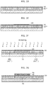
- FIGS. 4A-C are diagrams of details for annealing in FIG. 2F according to at least one embodiment.
- FIG. 5 is a graph of results of measuring a sheet resistance value in the case where fluorine is included in an oxide semiconductor layer, and a sheet resistance value in the case where fluorine is not included in the oxide semiconductor layer according to at least one embodiment.
- FIG. 6 is a cross-sectional view of a device structure of a sample used in an experiment for hydrogen resistance according to at least one embodiment.
- FIG. 7 is a graph, for the sample having the structure illustrated in FIG. 6 , of ⁇ -PCD peak intensity and a resistance value of the oxide semiconductor layer when a film thickness of a silicon oxide layer is varied according to at least one embodiment.
- FIG. 8 is a graph of results of comparing ⁇ -PCD peak intensity and the presence or absence of fluorine introduction to an oxide semiconductor layer according to at least one embodiment.
- FIG. 9A is a graph of an In3d5 XPS spectrum in the case where fluorine is included in an oxide semiconductor layer, and an In3d5 XPS spectrum in the case where fluorine is not included in the oxide semiconductor layer according to at least one embodiment.
- FIG. 9B is a graph of a Zn2p3 XPS spectrum in the case where fluorine is included in an oxide semiconductor layer, and a Zn2p3 XPS spectrum in the case where fluorine is not included in the oxide semiconductor layer according to at least one embodiment.
- FIG. 9C is a graph of a Ga2p3 XPS spectrum in the case where fluorine is included in an oxide semiconductor layer, and a Ga2p3 XPS spectrum in the case where fluorine is not included in the oxide semiconductor layer according to at least one embodiment.
- FIG. 10 is a graph of a Zn thermal desorption spectrum by TDS in the case where fluorine is included in an oxide semiconductor layer, and a Zn thermal desorption spectrum by TDS in the case where fluorine is not included in the oxide semiconductor layer according to at least one embodiment.
- FIG. 11 is a graph of resistance values of an oxide semiconductor film in the case where ALD is used and in the case where ALD is not used according to at least one embodiment.
- FIG. 12 is a cutaway perspective view of part of an organic EL display device according to at least one embodiment.
- FIG. 13 is an electric circuit diagram of a pixel circuit of the organic EL display device in FIG. 12 according to at least one embodiment.
- a thin film transistor includes a gate electrode.
- the TFT includes an oxide semiconductor layer which includes at least indium and is usable as a channel layer.
- the TFT includes a gate insulating layer disposed between the gate electrode and the oxide semiconductor layer.
- the TFT includes a fluorine-including layer which includes fluorine and is disposed between the gate electrode and the gate insulating layer. Fluorine is included in a region in the oxide semiconductor layer and close to the gate insulating layer.
- fluorine is included in the region in the oxide semiconductor layer and close to the gate insulating layer.
- Fluorine has higher binding energy with metal than oxygen. Accordingly, including fluorine in the oxide semiconductor layer enables fluorine to help eliminate dangling bonds or an unstable site caused by oxygen deficiency in the oxide semiconductor layer. In other words, including fluorine in the oxide semiconductor layer makes helps to compensate for the oxygen deficiency in the oxide semiconductor layer.
- including fluorine in the oxide semiconductor layer helps to prevent hydrogen entering the oxide semiconductor layer from bonding with the oxide semiconductor layer. With this, hydrogen is inhibited from entering the oxide semiconductor layer, thereby suppressing generation of charge carriers resulting from bonding of oxygen and hydrogen in the oxide semiconductor layer. In short, including fluorine in the oxide semiconductor layer helps to improve hydrogen resistance of the oxide semiconductor layer.
- including fluorine in the oxide semiconductor layer results in metallic elements included in the oxide semiconductor layer being chemically bonded with fluorine, which helps to stabilize a structure of the oxide semiconductor layer.
- the oxide semiconductor layer is less susceptible to damage resulting hydrogen or oxygen as well as stabilize the structure of the oxide semiconductor layer. With this, a thin film transistor having high reliability and high robustness is possible.
- the fluorine-including layer is disposed between the gate electrode and the gate insulating layer.
- Vth threshold voltage
- the gate insulating layer includes fluorine, and a fluorine concentration of the oxide semiconductor layer is higher than a fluorine concentration of the gate insulating layer.
- hydrogen entering the oxide semiconductor layer can be blocked by the oxide semiconductor layer.
- the fluorine-including layer may be a fluorine layer including only fluorine.
- the fluorine-including layer is formed on the gate insulating layer by supply of fluorine system gas.
- the gate insulating layer may include an inorganic material
- the fluorine-including layer may be an organic layer which includes fluorine and includes an organic material.
- the fluorine-including layer can be made of the organic layer including fluorine. With this, because the fluorine-including layer is physically adsorbed to the organic layer, fluorine is easily supplied to the oxide semiconductor layer from the fluorine-including layer.
- the fluorine-including layer and the gate insulating layer may include a same main element, and a peak position of an X-ray photoelectron spectroscopy spectrum of the main element in the fluorine-including layer may be closer to a high binding energy side than a peak position of an X-ray photoelectron spectroscopy spectrum of the main element in the gate insulating layer is.
- fluorine in the fluorine-including layer is more chemically boned with the main element than fluorine in the gate insulating layer is.
- a fluorine concentration of a region close to the gate insulating layer may be higher than a fluorine concentration of a region far from the gate insulating layer.
- a portion of the region that is in the oxide semiconductor layer and close to the gate insulating layer (fluorine-including layer) is an oxygen deficient region, and only this region is compensated with fluorine.
- fluorine-including layer a portion of the region that is in the oxide semiconductor layer and close to the gate insulating layer (fluorine-including layer)
- a method for manufacturing a thin film transistor includes forming an oxide semiconductor film including indium, above a substrate.
- the method further includes forming a gate insulating layer above the oxide semiconductor film.
- the method further includes forming a fluorine-including layer above the gate insulating layer.
- the method further includes forming a gate electrode above the fluorine-including layer.
- the method further includes annealing, after the fluorine-including layer is formed, the fluorine-including layer to diffuse fluorine from the fluorine-including layer into the oxide semiconductor film.
- oxygen deficiency in the oxide semiconductor film can be compensated with fluorine by diffusing fluorine from the fluorine-including layer into the oxide semiconductor film.
- the oxide semiconductor layer has superior hydrogen resistance as well as a stable structure. Accordingly, a thin film transistor having high reliability and high robustness is possible.
- the gate insulating layer which includes an element as a main component may be deposited on the oxide semiconductor film by supplying reactive gas containing molecules including an alkyl group and the element included in the gate insulating layer.
- the oxide semiconductor film is in a low resistance state.
- low resistance regions a source region and a drain region are formed in the oxide semiconductor film without using plasma or hydrogen.
- the fluorine-including layer may be formed above a portion of the oxide semiconductor film, and in the annealing, fluorine may be diffused into the portion of the oxide semiconductor film and bonded with the oxide semiconductor film, the portion being covered with the fluorine-including layer and included in a region of the oxide semiconductor film from which the reactive gas supplied when the gate insulating layer is deposited desorbs oxygen.
- fluorine is diffused into the portion of the oxide semiconductor covered with the fluorine-including layer, whereas fluorine is not diffused into portions of the oxide semiconductor film not covered with the fluorine-including layer.
- the portion covered with the fluorine-including layer is compensated with fluorine, and the portions not covered with the fluorine-including layer are not compensated with fluorine and are kept in a low resistance state.
- a thin film transistor has the source region and the drain region on the respective sides of the channel region.
- the source region and the drain region are formed in a self-aligning manner.
- FIG. 1 is a cross-sectional view of a structure of a thin film transistor according to at least one embodiment of the present description.
- the thin film transistor 1 is a top gate oxide semiconductor TFT having an oxide semiconductor layer as a channel layer.
- the thin film transistor 1 includes: a substrate 10 ; an undercoat layer 20 ; an oxide semiconductor layer 30 usable as a channel layer; an oxide semiconductor layer 40 S usable as a source region; an oxide semiconductor layer 40 D usable as a drain region; a gate insulating layer 50 ; a fluorine-including layer 60 ; a gate electrode 70 ; an interlayer insulating layer 80 ; and a source electrode 90 S and a drain electrode 90 D.
- the substrate 10 is a glass substrate including a glass material such as quartz glass, alkali-free glass, and high heat-resistant glass.
- the substrate 10 is not limited to the glass substrate and may be a resin substrate or the like.
- the substrate 10 is not a rigid substrate but may be a flexible substrate including a single layer of a film material such as polyimide, polyethylene terephthalate, and polyethylene naphthalate, or stacked layers of these.
- the undercoat layer 20 is formed on the substrate 10 .
- the undercoat layer 20 is formed to help prevent impurities such as sodium and phosphorus included in the substrate 10 (glass substrate) or moisture permeated from the air from entering the oxide semiconductor layers 30 , 40 S, and 40 D.
- the undercoat layer 20 is a single layer insulating layer of an oxide insulating layer or a nitride insulating layer, or a stacked insulating layer including an oxide insulating layer and a nitride insulating layer.
- a single layer film of silicon nitride (SiN x ), silicon oxide (SiO y ), silicon oxynitride (SiO y N x ), or aluminum oxide (AlO x ), or stacked films of these can be used as the undercoat layer 20 .
- the film thickness of the undercoat layer 20 is set to be from 100 to 500 nm. In at least one embodiment, undercoat layer 20 is omitted.
- the oxide semiconductor layer 30 is usable as a channel layer.
- the oxide semiconductor layer 30 is a semiconductor layer including a channel region opposing the gate electrode 70 with the gate insulating layer 50 being between the channel region and the gate electrode 70 .
- the oxide semiconductor layer 30 is formed at a position opposite the gate electrode 70 with the gate insulating layer 50 and the fluorine-including layer 60 being between the oxide semiconductor layer 30 and the gate electrode 70 .
- the oxide semiconductor layer 40 S is a semiconductor layer usable as a source region provided on one side of the oxide semiconductor layer 30 .
- the oxide semiconductor layer 40 D is a semiconductor layer usable as a drain region provided on the other side of the oxide semiconductor layer 30 .
- the oxide semiconductor layers 40 S and 40 D each are a low resistance region (offset region) having a resistance value lower than that of the oxide semiconductor layer 30 .
- a resistance value of an upper region is less than that of a lower region (region closer to a side of the undercoat layer 20 ).
- the resistance values differ from each other in a stack direction, and the resistance value of the upper layer portion is less than that of the lower layer portion.
- the oxide semiconductor layers 40 S and 40 D in at least one embodiment are placed in a low resistance state by desorption of oxygen.
- the oxide semiconductor layers 30 , 40 S, and 40 D are formed in a predetermined shape, on the undercoat layer 20 . Moreover, the oxide semiconductor layers 30 , 40 S, and 40 D include the same material. A transparent amorphous oxide semiconductor (TAOS) is used for the material of the oxide semiconductor layers 30 , 40 S, and 40 D, for example.
- TAOS transparent amorphous oxide semiconductor
- metallic elements included in each of the oxide semiconductor layers 30 , 40 S, and 40 D include at least indium (In) and further at least one or both of gallium (Ga) and zinc (Zn).
- the oxide semiconductor layers 30 , 40 S, and 40 D in at least one embodiment each include InGaZnO x (IGZO), that is, an oxide including indium (In), gallium (Ga), and zinc (Zn).
- IGZO InGaZnO x
- the oxide semiconductor layer 30 includes fluorine (F). Specifically, fluorine is included in a region that is an internal region in the oxide semiconductor layer 30 and is close to the gate insulating layer 50 . In other words, fluorine is included on a front channel side of the oxide semiconductor layer 30 , and fluorine is included on a side of the gate insulating layer 50 in the oxide semiconductor layer 30 . In contrast, the oxide semiconductor layers 40 S and 40 D include no fluorine.
- Fluorine that is chemically bonded is included in the oxide semiconductor layer 30 .
- the region that is the internal region in the oxide semiconductor layer 30 and is close to the gate insulating layer 50 is a region that is on the side of the gate insulating layer 50 and is above at least the middle of a thickness of the oxide semiconductor layer 30 .
- the oxide semiconductor layer 30 in at least one embodiment includes a first region (fluorine-including region) which is a region including fluorine, and a second region (no-fluorine-including region) which is a region including no fluorine.
- the first region in the oxide semiconductor layer 30 is a region (upper layer) above the middle of the film thickness of the oxide semiconductor layer 30
- the second region in the oxide semiconductor layer 30 is a region (lower layer) below the middle of the film thickness of the oxide semiconductor layer 30 .
- the first region, the upper layer, in the oxide semiconductor layer 30 is a region on the side of the gate insulating layer 50 (front channel side) in the oxide semiconductor layer 30 .
- fluorine is included only in the region on the side of the gate insulating layer 50 (side of the gate electrode 70 ) in the oxide semiconductor layer 30 .
- the second region, the lower layer, in the oxide semiconductor layer 30 is a region on the side of the substrate 10 (back channel side) in the oxide semiconductor layer 30 .
- the region on the side of the gate insulating layer 50 has a fluorine concentration higher than that of the region on the side of the undercoat layer 20 .
- the fluorine-including region in the oxide semiconductor layer 30 may have a thickness of at least 5 nm. In at least one embodiment, the fluorine-including region has a thickness of at least 15 nm. In at least one embodiments, the fluorine-including region has a thickness of at least 20 nm. Moreover, the oxide semiconductor layer 30 may have, as a whole, a film thickness of at least 20 nm.
- the film thickness of the fluorine-including region in the oxide semiconductor layer 30 helps to sufficiently exert the aforementioned effect of including fluorine.
- the film thickness of the fluorine-including region in the oxide semiconductor layer 30 is at least 15 nm , and thus hydrogen entering the oxide semiconductor layer 30 from the side of the gate insulating layer 50 can be effectively blocked. With this, stable thin film transistor characteristics are obtained.
- setting the film thickness of the fluorine-including region in the oxide semiconductor layer 30 to be at least 20 nm helps to sufficiently perform process control of the oxide semiconductor layer 30 .
- setting the film thickness of the fluorine-including region in the oxide semiconductor layer 30 to be at least 20 nm helps to set the film thickness of the oxide semiconductor layer 30 as a whole to be at least 20 nm.
- the device characteristics of the oxide semiconductor layer 30 deteriorate when the oxide semiconductor layer 30 is damaged by hydrogen annealing
- the device characteristics can be recovered by etching 20 nm from the hydrogen-exposed surface.
- the fluorine-including region in the oxide semiconductor layer 30 may be have a film thickness of at least 20 nm.
- the film thickness of the oxide semiconductor layer 30 as a whole makes helps to obtain stable device characteristics as a TFT.
- the oxide semiconductor layer 30 has a fluorine concentration higher than that of the gate insulating layer 50 .
- the oxide semiconductor layer 30 has a fluorine concentration higher than a hydrogen concentration of the oxide semiconductor layer 30 .
- the oxide semiconductor layer 30 has a fluorine concentration of at least 1 ⁇ 10 22 atm/cm 3 .
- the gate insulating layer 50 (insulating layer) is formed above the oxide semiconductor layers 30 , 40 S, and 40 D.
- the gate insulating layer 50 is, for example, a single layer insulating layer of an oxide insulating layer or a nitride insulating layer, or a stacked insulating layer including an oxide insulating layer and a nitride insulating layer.
- the gate insulating layer 50 may be a single layer film of silicon oxide, aluminum oxide (alumina), silicon nitride, silicon oxynitride, tantalum oxide, or the like, or stacked films of these.
- the gate insulating layer 50 having a stacked layer structure may be stacked films of a silicon oxide film and an aluminum oxide film (alumina film).
- the film thickness of the insulating layer 50 can be designed by taking into consideration pressure resistance of the TFT or the like, and in at least one embodiment ranges from 50 to 500 nm, for example.
- the gate insulating layer 50 is formed by atomic layer deposition (ALD).
- ALD atomic layer deposition
- the gate insulating layer 50 is deposited by causing a surface chemical reaction in the interface of an oxide semiconductor film by supplying the oxide semiconductor film with reactive gas containing molecules (precursors) including an alkyl group (—C n H 2n+1 ) and elements included in the gate insulating layer 50 .
- a silicon oxide film SiO film
- tris(dimethylamino)silane C 6 H 19 N 3 Si
- tetraethoxysilane Si(OC 2 H 5 ) 4
- AlO x film aluminum oxide film
- Al(CH 3 ) 3 trimethylaluminum
- the gate insulating layer 50 may be formed by another method such as plasma CVD, instead of ALD.
- the gate insulating layer 50 sometimes includes fluorine.
- fluorine included in the gate insulating layer 50 is fluorine diffused from the fluorine-including layer 60 , and is thought to be chemically adsorbed to dangling bonds in the gate insulating layer 50 .
- fluorine in the gate insulating layer 50 is thought to be chemically bonded with the elements constituting the gate insulating layer 50 .
- some fluorine in the gate insulating layer 50 is thought to be physically adsorbed, chemically bonded fluorine in the gate insulating layer 50 is thought to be more dominant.
- the fluorine-including layer 60 is a layer including at least fluorine (F). Moreover, the fluorine-including layer 60 functions as a fluorine-supplying layer that supplies other layers with fluorine by fluorine included in the fluorine-including layer 60 being diffused by subsequent annealing. As described later, fluorine in the fluorine-including layer 60 compensates oxygen deficiency in the oxide semiconductor film by being diffused into the oxide semiconductor film by annealing.
- the fluorine-including layer 60 in at least one embodiment is an insulating layer made of an insulating material.
- the fluorine-including layer 60 may be a fluorine layer including only fluorine or an organic layer which includes fluorine and is made of an organic material.
- the fluorine-including layer 60 is the fluorine layer, for example, the fluorine-including layer 60 is a layer obtained by fluorine being physically adsorbed above the oxide semiconductor layer 30 .
- fluorine-including layer 60 when the fluorine-including layer 60 is the organic layer, fluorine is physically adsorbed in the organic material (organic layer).
- organic material examples include a resin material such as CYTOP.
- the fluorine-including layer 60 the organic layer, may include both fluorine physically adsorbed to the organic layer and fluorine physically bonded with the organic material of the organic layer.
- fluorine physically adsorbed is more dominant than fluorine chemically bonded with the organic material.
- the gate insulating layer 50 may be an inorganic layer includes an inorganic material such as a resin material.
- the gate insulating layer 50 is, for example, a silicon oxide layer or an aluminum oxide layer.
- XPS X-ray photoelectron spectroscopy
- the fluorine-including layer 60 is formed at a position opposite the oxide semiconductor layer 30 with the gate insulating layer 50 being between the fluorine-including layer 60 and the oxide semiconductor layer 30 .
- the fluorine-including layer 60 is disposed between the gate insulating layer 50 and the gate electrode 70 .
- a channel direction length of the fluorine-including layer 60 is almost identical to a channel direction length of the oxide semiconductor layer 30 and a channel direction length of the gate electrode 70 .
- both side surfaces of the fluorine-including layer 60 are flush with both side surfaces of the oxide semiconductor layer 30 as well as both side surfaces of the gate electrode 70 .
- the gate electrode 70 , the fluorine-including layer 60 , and the oxide semiconductor layer 30 may be formed to completely overlap with each other. In this case, the fluorine-including layer 60 does not overlap with the oxide semiconductor layers 40 S and 40 D, and the oxide semiconductor layers 40 S and 40 D are not below the fluorine-including layer 60 .
- the gate electrode 70 is formed at a position opposite the oxide semiconductor layer 30 with the gate insulating layer 50 being between the gate electrode 70 and the oxide semiconductor layer 30 .
- the gate electrode 70 is formed at a position opposite the oxide semiconductor layer 30 with the gate insulating layer 50 and the fluorine-including layer 60 being between the gate electrode 70 and the oxide semiconductor layer 30 .
- the gate electrode 70 is formed in a predetermined shape, on the fluorine-including layer 60 .
- the gate electrode 70 is an electrode having a single layer structure or a multi-layer structure including a conductive material such as metal or an alloy thereof, and may include molybdenum (Mo), aluminum (Al), copper (Cu), tungsten (W), titanium (Ti), chrome (Cr), or molybdenum tungsten (MoW), for example.
- the film thickness of the gate electrode 70 is set to be from 50 to 300 nm.
- the interlayer insulating layer 80 is formed to cover the gate electrode 70 and the oxide semiconductor layers 40 S and 40 D.
- the interlayer insulating layer 80 may be made of a material including an organic substance as a main component or may include an inorganic substance such as silicon oxide, silicon nitride, silicon oxynitride, and aluminum oxide.
- the interlayer insulating layer 80 may be a single layer film or a film having stacked layers.
- the interlayer insulating layer 80 having a stacked layer structure may be, for example, stacked films of a silicon oxide film and an aluminum oxide film.
- openings are formed to penetrate part of the interlayer insulating layer 80 .
- the oxide semiconductor layer 40 S is connected to the source electrode 90 S, and the oxide semiconductor layer 40 D is connected to the drain electrode 90 D, via the openings of the interlayer insulating layer 80 .
- the source electrode 90 S and the drain electrode 90 D are formed in a predetermined shape, on the interlayer insulating layer 80 . Moreover, the source electrode 90 S and the drain electrode 90 D are each electrically connected to the oxide semiconductor layer 30 . In the embodiment, the source electrode 90 S and the drain electrode 90 D are each electrically and physically connected to a different one of the oxide semiconductor layers 40 S and 40 D via the openings formed in the interlayer insulating layer 80 , and are electrically connected to the oxide semiconductor layer 30 via the oxide semiconductor layers 40 S and 40 D.
- the source electrode 90 S and the drain electrode 90 D each are an electrode having a single layer structure including an conductive material or an alloy thereof, or a stacked layer structure of these.
- the source electrode 90 S and the drain electrode 90 D may include, for example, molybdenum (Mo), aluminum (Al), copper (Cu), tungsten (W), titanium (Ti), chrome (Cr), molybdenum tungsten alloy (MoW), or copper manganese allow (CuMn).
- the film thickness of the source electrode 90 S and the drain electrode 90 D is set to be from 50 to 300 nm, for example.
- FIGS. 2A to 2I are cross-sectional views of processes in the method for manufacturing the thin film transistor according to at least one embodiment of the present description.
- the substrate 10 is prepared.
- a glass substrate is used as the substrate 10 , for example.
- the undercoat layer 20 is formed on the substrate 10 .
- the undercoat layer 20 including a silicon nitride film, a silicon oxide film, a silicon oxynitride film, an aluminum oxide film, or the like is formed on the substrate 10 by plasma chemical vapor deposition (CVD) or the like.
- an oxide semiconductor film SC is deposited on the undercoat layer 20 .
- the oxide semiconductor film SC may include an InGaZnO x transparent amorphous oxide semiconductor.
- the oxide semiconductor film (InGaZnO x film) SC including InGaZnO x can be deposited by a vapor deposition method such as a sputtering method or a laser evaporation method.
- a target material including In, Ga, and Zn for example, a polycrystalline sintered body having an InGaO 3 (ZnO) 4 composition
- an argon (Ar) gas as an inert gas and a gas including oxygen (O 2 ) as a reactive gas are introduced into a vacuum chamber, and voltage of a predetermined power density is applied to the target material.
- the oxide semiconductor film SC can be formed in a predetermined shape by patterning the oxide semiconductor film SC using a photolithography or wet etching method.
- a resist having a predetermined shape is formed on the oxide semiconductor film SC, and part of the oxide semiconductor film SC in a region where the resist is not formed is removed by wet etching, thereby forming the oxide semiconductor film SC having an island shape.
- the oxide semiconductor film SC includes InGaZnO x
- a chemical solution obtained by mixing, for example, phosphoric acid (H 3 PO 4 ), nitric acid (HNO 3 ), acetic acid (CH 3 COOH), and water may be used as an etching solution.
- the gate insulating layer 50 is formed on the oxide semiconductor film SC.
- the gate insulating layer 50 is, for example, a silicon nitride film, a silicon oxide film, a silicon oxynitride film, a tantalum oxide film, an aluminum oxide film, or stacked layers of these.
- the gate insulating layer 50 is deposited by ALD. Specifically, the gate insulating layer 50 is deposited as a whole on a top surface of the oxide semiconductor film SC by ALD. Processing costs are reduced by depositing the gate insulating layer 50 as a whole.
- the gate insulating layer 50 may be deposited not by ALD but by plasma CVD.
- the SiO film can be deposited using a mixture gas of monoslinae (SiH 4 ) and nitrous oxide (N 2 O).
- the SiO film is deposited by plasma CVD, the SiO film is deposited by SiH 4 gas and N 2 O gas being reacted with each other in a vapor phase, but, in this case, unlike ALD, a reaction does not occur in which the oxide semiconductor film SC is placed in the low resistance state. Accordingly, when a source region and a drain region are formed in the oxide semiconductor film SC, part of the oxide semiconductor film SC is placed in the low resistance state by separately performing plasma processing etc.
- the fluorine-including layer 60 is formed on the gate insulating layer 50 .
- the fluorine-including layer 60 is formed on the gate insulating layer 50 above a region of an oxide semiconductor film SC° ⁇ .
- the fluorine-including layer 60 is formed only above a portion of the oxide semiconductor film SC° ⁇ that is to be a channel region.
- the fluorine-including layer 60 can be formed by performing, while supplying fluorine system gas, annealing treatment or discharge treatment to adsorb fluorine on the gate insulating layer 50 .
- the fluorine-including layer 60 is formed as a layer obtained by fluorine being physically adsorbed to a surface of the gate insulating layer 50 .
- fluorine system gas may be supplied after a mask is placed to cover a portion of the gate insulating layer 50 (portion in which the fluorine-including layer 60 is not formed).
- fluorine-including layer 60 only above the portion of the oxide semiconductor film SC° ⁇ that is to be the channel region.
- the organic layer including fluorine is formed by forming an organic layer by applying an organic material to only a predetermined region of the gate insulating layer 50 , and by adsorbing fluorine to the organic layer.
- a method for forming the fluorine-including layer 60 is not limited to a method by which fluorine of the fluorine-including 60 is diffused into the oxide semiconductor film SC° ⁇ via the gate insulating layer 50 in subsequent annealing.
- the fluorine-including layer 60 is annealed after the fluorine-including layer 60 is formed.
- This annealing causes fluorine to diffuse (thermal diffuse) from the fluorine-including layer 60 , and to be chemically bonded in the oxide semiconductor film SC° ⁇ .
- An annealing temperature may be at least a temperature at which fluorine adsorbed to the fluorine-including layer 60 on the gate insulating layer 50 starts to desorb, and is, for example, 300° C.
- FIG. 4 is a diagram for describing the details of the annealing in FIG. 2F .
- the fluorine-including layer 60 is formed only above a region of the oxide semiconductor film SC° ⁇ .
- the annealing causes fluorine to thermally diffuse only into a portion covered with the fluorine-including layer 60 and included in the region of the oxide semiconductor film SC° ⁇ (region in which the reactive gas when the gate insulating layer 50 is deposited causes oxygen to desorb from the oxygen semiconductor film SC), and to be chemically bonded in the oxide semiconductor film SC° ⁇ . Accordingly, oxygen deficiency in the oxide semiconductor film SC° ⁇ caused when the gate insulating layer 50 is deposited by ALD is compensated for with fluorine diffused from the fluorine-including layer 60 .
- portions of the oxide semiconductor film SC° ⁇ not covered with the fluorine-including layer 60 remain low resistance regions and become the oxide semiconductor layers 40 S and 40 D respectively functioning as the source region and the drain region.
- fluorine is not actively diffused into the oxide semiconductor layers 40 S and 40 D, when fluorine is diffused into the oxide semiconductor layer 30 , fluorine may naturally go into the oxide semiconductor layers 40 S and 40 D. Accordingly, surface layers or regions of the oxide semiconductor layers 40 S and 40 D neighboring the oxide semiconductor layer 30 may slightly include fluorine.
- the fluorine-including layer 60 is either the fluorine layer or the organic layer including fluorine
- the fluorine-including layer 60 is present after the annealing.
- the fluorine-including layer 60 still includes fluorine after the annealing.
- the oxide semiconductor layer 30 is selectively formed as usable as the channel layer, the oxide semiconductor layer 40 S to be the source region, and the oxide semiconductor layer 40 D to be the drain region, by compensating, with fluorine, the oxygen deficiency in the portion of the oxide semiconductor film SC° ⁇ caused when the gate insulating layer 50 is deposited by ALD, and by intentionally leaving the other portions thereof without compensating the other portions with fluorine.
- the source region (oxide semiconductor layer 40 S) and the drain region (oxide semiconductor layer 40 D) are formed in a self-aligning manner, by selectively compensating, with fluorine, the oxygen deficiency in the portion of the oxide semiconductor film SC° ⁇ , and by leaving the other portions with the oxygen deficiency as the low resistance regions.
- fluorine diffuses from the fluorine-including layer 60 into the oxide semiconductor film SC° ⁇ , see FIGS. 4A-C .
- fluorine passes through the gate insulating layer 50 .
- fluorine may be present in the gate insulating layer 50 by being captured by dangling bonds (defects) in the gate insulating layer 50 .
- dangling bonds in the gate insulating layer 50 are terminated with fluorine by diffusing fluorine via the gate insulating layer 50 .
- a peak position of an F1S XPS spectrum in the fluorine-including layer 60 shifts closer to the high biding energy side after the annealing than before the annealing. Accordingly, after the annealing, chemically bonded fluorine seems to be more dominant than physically bonded fluorine in the fluorine-including layer 60 .
- a peak position of an Si2p XPS spectrum in the gate insulating layer 50 shifts closer to the high binding energy side after the annealing than before the annealing. This is because the annealing seems to have caused fluorine to be chemically bonded in the gate insulating layer 50 .
- the gate electrode 70 is formed on the fluorine-including layer 60 .
- the gate electrode 70 is formed only above the fluorine-including layer 60 and the oxide semiconductor layer 30 , but the embodiment is not limited to this.
- the gate electrode 70 is formed in a predetermined shape by depositing, by sputtering, a metal film (gate metal film) including molybdenum tungsten (MoW), and then by patterning the metal film using a photolithography or wet etching method.
- a chemical solution can be used which is obtained by mixing, for example, phosphoric acid (HPO 4 ), nitric acid (HNO 3 ), acetic acid (CH 3 COOH), and water in a predetermined combination ratio.
- the interlayer insulating layer 80 is formed to cover the gate insulating layer 50 and the gate electrode 70 .
- the interlayer insulating layer 80 may include an organic substance as a main component or an inorganic substance such as a silicon oxide film.
- a silicon oxide film may be deposited as the interlayer insulating layer 80 by plasma CVD.
- the openings are formed in the interlayer insulating layer 80 to expose part of each of the oxide semiconductor layers 40 S and 40 D. Specifically, part of the interlayer insulating layer 80 is etched away by a photolithography or etching method, thereby forming the openings above connection portions with the source electrode 90 S and the drain electrode 90 D in the respective oxide semiconductor layers 40 S and 40 D.
- the openings can be formed in the silicon oxide film by a dry etching method such as a reactive ion etching (RIE) method.
- RIE reactive ion etching
- carbon tetrafluoride (CF 4 ) and oxygen gas (O 2 ) for example, can be used as etching gas.
- the source electrode 90 S and the drain electrode 90 D are formed which are connected to the oxide semiconductor layers 40 S and 40 D via the openings formed in the interlayer insulating layer 80 .
- the source electrode 90 S and the drain electrode 90 D having a predetermined shape are formed by depositing, by sputtering, a metal film (source-drain metal film) on the interlayer insulating layer 80 to fill the openings formed in the interlayer insulating layer 80 , and then by patterning the metal film using the photolithography or wet etching method.
- a heat treatment at 300° C. (annealing) is performed subsequently.
- This heat treatment makes it possible to reduce oxygen deficiency in the oxide semiconductor layer 30 to stabilize characteristics of the oxide semiconductor layer 30 .
- the following describes an operational effect of the thin film transistor 1 according to at least one embodiment together with the background to the present description.
- bottom-gate oxide semiconductor TFTs but also top-gate oxide semiconductor TFTs have been much developed, the bottom-gate oxide semiconductor TFTs being highly compatible with amorphous silicon TFTs for liquid crystal display, the top-gate oxide semiconductor TFTs having merits of, for example, being easily miniaturized and having small parasitic capacitance.
- Non Patent Literature (NPL) 1 describes a top-gate TFT in which a gate insulating layer and a gate electrode are formed in the same shape, on a channel region in an oxide semiconductor layer, and a source region and a drain region are formed by placing, into a low resistance state, a region not covered with the gate insulating layer and the gate electrode in the oxide semiconductor layer.
- a difficulty in manufacturing the top-gate TFT is how low resistance regions (the source region and the drain region) are formed in the oxide semiconductor layer.
- the source region and the drain region are formed by placing the oxide semiconductor layer into the low resistance state by being exposed to plasma atmosphere including argon gas.
- a bottom-gate TFT disclosed by Patent Literature (PTL) 2 uses both hydrogen introduction from a silicon nitride film and plasma processing with hydrogen gas when a source region and a drain region are formed by placing an oxide semiconductor layer into a low resistance state.
- Non Patent Literature (NPL) 2 because an oxide semiconductor layer is very sensitive to hydrogen, a variation in device characteristics or degradation of reliability is caused by process damage resulting from hydrogen or the like in a manufacturing process.
- the present description has been conceived based on such knowledge, and the inventor of at least one embodiment of the present description has arrived at an idea of obtaining a thin film transistor having high reliability by forming a fluorine-including layer and diffusing fluorine from the fluorine-including layer into the oxide semiconductor layers 30 , 40 S, and 40 D as described above.
- the inventor thereof has found a method for forming a low resistance region in an oxide semiconductor layer without using hydrogen or plasma processing, and has succeeded in achieving a thin film transistor including an oxide semiconductor layer having a channel region having high stability, and a source region and a drain region formed with no damage to plasma and hydrogen.
- the inventor has conducted various experiments to verify whether a thin film transistor having high reliability is obtained by including fluorine in an oxide semiconductor layer.
- the following describes the experiments and analyses thereof.
- an InGaZnO x film whose main components of metallic elements are In, Ga, and Zn is used as the oxide semiconductor layer.
- FIG. 5 is a graph of the results of measuring, using four-terminal sensing, a sheet resistance value in vacuum heating (300° C.) for the case where fluorine is included in the oxide semiconductor layer and the case where fluorine is not included in the oxide semiconductor layer.
- Charge carriers are generated by oxygen deficiency (desorption of oxygen) to decrease a resistance value of the oxide semiconductor layer.
- a sheet resistance value in the case where fluorine is not included in the oxide semiconductor layer is low such as approximately 1 ⁇ 10 5 ⁇ / ⁇ .
- a sheet resistance value in the case where fluorine is included in the oxide semiconductor layer is a measurement limit (>1 ⁇ 10 10 ⁇ / ⁇ ) and is higher than the sheet resistance value in the case fluorine is not included in the oxide semiconductor layer.
- fluorine since fluorine has higher binding energy with metal than oxygen, including fluorine in the oxide semiconductor layer enables fluorine to eliminate dangling bonds or an unstable site caused by the oxygen deficiency in the oxide semiconductor layer.
- FIG. 6 is a cross-sectional view of a device structure of a sample used in an experiment for hydrogen resistance according to at least one embodiment.
- a sample in the experiment, which has a three layer structure in which an oxide semiconductor layer (IGZO), a silicon oxide layer (SiO), and a silicon nitride layer (SiN:H) including hydrogen are stacked above a glass substrate.
- IGZO oxide semiconductor layer
- SiO silicon oxide layer
- SiN:H silicon nitride layer
- FIG. 7 is a graph, for the sample having the structure in FIG. 6 , of ⁇ -PCD peak intensity and a resistance value of the oxide semiconductor layer when the film thickness of the silicon oxide layer is varied.
- the film thickness of the silicon oxide layer is varied to 10 nm, 120 nm, and 240 nm.
- the resistance value of the oxide semiconductor layer is measured by a non-contact resistance measurement device.
- the resistance value of the oxide semiconductor layer (IGZO) and the ⁇ -PCD peak intensity give an indication of determining hydrogen-induced damage due to the presence or absence of fluorine introduction.
- FIG. 8 is a graph of the results of comparing ⁇ -PCD peak intensity and the presence or absence of fluorine introduction to an oxide semiconductor layer.
- a ⁇ -PCD intensity value (a ratio of a peak intensity value before depositing SiN: H film to a peak intensity value after depositing SiN: H film) in the oxide semiconductor layer decreases.
- a resistance value barely varies even if fluorine is introduced when the resistance value is low, that is, the resistance value does not decrease.
- the included hydrogen bonds with oxygen in the oxide semiconductor layer to generate charge carriers.
- FIGS. 9A to 9C are each a graph of a corresponding one of In3d5, Zn1p3, and Ga2p3 XPS spectra in the case where fluorine is included in an oxide semiconductor layer (IGZO) (IGZO including F) and a corresponding one of In3d5, Zn1p3, and Ga2p3 XPS spectra in the case where fluorine is not included in an oxide semiconductor layer (IGZO) (IGZO including no F).
- IGZO oxide semiconductor layer
- IGZO oxide semiconductor layer
- the inclusion of fluorine causes a peak position of the In3d5 XPS spectrum to shift to a high binding energy side by at least 0.5 eV.
- a peak position of In3d5 in IGZO including F measured by XPS is shifted to the high binding energy side by at least 0.5 eV in comparison to a peak position of In3d5 in IGZO including no F.
- the inclusion of fluorine causes a peak position of the Zn2p3 XPS spectrum to shift to the high binding energy side by at least 0.4 eV.
- a peak position of Zn2p3 in IGZO including F measured by XPS is shifted to the high binding energy side by at least 0.4 eV in comparison to a peak position of Zn2p3 in IGZO including no F.
- the inclusion of fluorine causes a peak position of the Ga2p3 XPS spectrum to shift to the high binding energy side by at least 0.5 eV.
- a peak position of Ga2p3 in IGZO including F measured by XPS is shifted to the high binding energy side by at least 0.5 eV in comparison to a peak position of Ga2p3 in IGZO including no F.
- FIGS. 9A to 9C indicate that including fluorine in the oxide semiconductor layer results in not merely fluorine being physically in the oxide semiconductor layer but in fluorine being chemically bonded with elements included in the oxide semiconductor layer. Consequently, the metallic elements included in the oxide semiconductor layer are less likely to escape.
- including fluorine in the oxide semiconductor layer results in the metallic elements included in the oxide semiconductor layer being chemically bonded with fluorine, which helps to stabilize the structure of the oxide semiconductor layer. With this, a thin film transistor having high reliability is possible.
- FIG. 10 is a graph of a Zn thermal desorption spectrum by thermal desorption spectrometry (TDS) in the case where fluorine is included in the oxide semiconductor layer (IGZO) (IGZO including F) and a Zn thermal desorption spectrum by TDS in the case where fluorine is not included therein (IGZO including no F).
- the oxide semiconductor layer in the case where fluorine is included therein has a fluorine concentration of 1 ⁇ 10 22 atm/cm 3 or more.
- the horizontal axis indicates a temperature (° C.) at which Zn undergoes thermal desorption
- the vertical axis indicates an amount of Zn undergoing thermal desorption (arbitrary unit).
- the thermal desorption of Zn in the oxide semiconductor layer (IGZO including F) in the case where fluorine is included therein occurs at a temperature higher by at least 50° C. in comparison to the thermal desorption of Zn in the oxide semiconductor layer (IGZO including no F) in the case where fluorine is not included therein.
- including fluorine in the oxide semiconductor layer so that the fluorine concentration is at least 1 ⁇ 10 22 atm/cm 3 causes the temperature (thermal desorption temperature) at which Zn undergoes the thermal desorption to increase by 50° C.
- a thermal desorption temperature can be used as a physical property index of an oxide semiconductor layer, and an increase in the thermal desorption temperature indicates that a structure of the oxide semiconductor layer is stabilized.
- the oxygen deficiency in the oxide semiconductor layer 30 is compensated for to improve the hydrogen resistance of the oxide semiconductor layer 30 and further stabilize the structure of the oxide semiconductor layer 30 .
- an insulating layer is formed by chemical reaction in an interface of an oxide semiconductor film caused by supplying reactive gas containing molecules including an alkyl group, and accordingly a source region and a drain region can be formed only by reaction of oxygen deficiency in a top surface of the oxide semiconductor film without using plasma or diffusion of hydrogen.
- the InGaZnO x film is used as the oxide semiconductor film (oxide semiconductor layer) in the following experiment as well.
- FIG. 11 is a graph of resistance values of an oxide semiconductor film in the case where ALD is used and in the case where ALD is not used.
- “No processing” indicates a sheet resistance value of an IGZO film (no heating) deposited by plasma CVD
- “Vacuum heat treatment” indicates a sheet resistance value of an IGZO film (left under atmosphere of 150° C.) deposited by plasma CVD
- “ALD AlO” indicates a sheet resistance value of AlO x film deposited by ALD using as trimethylaluminum a precursor
- ALD SiO indicates a sheet resistance value of an SiO film deposited by ALD using tris(dimethylamino)silane as a precursor.
- the sheet resistance values are a measurement limit (>1E+10 [ ⁇ / ⁇ ]). Moreover, the sheet resistance values are almost identical between the cases of “No processing” and “Vacuum heat treatment.” The application of heat at approximately 150° C. does not cause the oxygen deficiency in the IGZO film, and the resistance value does not vary.
- the oxide semiconductor layer 30 may have a fluorine concentration higher than a carbon concentration of the oxide semiconductor layer 30 . Accordingly, sufficiently compensating for the oxygen deficiency in the oxide semiconductor film with fluorine due to carbon is possible.
- fluorine is included in a region that is in the oxide semiconductor layer 30 and close to the gate insulating layer 50 .
- the oxygen deficiency in the oxide semiconductor layer 30 is compensated for with fluorine. Moreover, improving the hydrogen resistance of the oxide semiconductor layer 30 is possible.
- the structure of the oxide semiconductor layer 30 is stabilized. Accordingly, a thin film transistor having high reliability and high robustness is possible.
- the fluorine-including layer 60 is disposed between the gate electrode 70 and the gate insulating layer 50 .
- Vth threshold voltage
- fluorine is not included in the oxide semiconductor layers 40 S and 40 D to be the source region and the drain region, respectively.
- the oxygen deficiency is caused in the oxide semiconductor film, and the oxide semiconductor layer 40 S (source region) and the oxide semiconductor layer 40 D (drain region) are formed, by placing the oxide semiconductor film into the low resistance state without using plasma or hydrogen.
- an oxygen deficient region (low resistance region) is formed in the oxide semiconductor film SC by carbon when the gate insulating layer 50 is deposited by ALD causing oxygen to desorb, and subsequently fluorine is thermally diffused into the oxygen deficient region of the oxide semiconductor film. Accordingly, the oxide semiconductor film placed in the low resistance state (conductive state) by carbon included in process gas is compensated with fluorine once, which makes it possible to restore the function as the semiconductor layer to the oxide semiconductor film.
- the region that is in the oxide semiconductor layer 30 and close to the gate insulating layer 50 has a fluorine concentration higher than that of a region that is in the oxide semiconductor layer 30 and far from the gate insulating layer 50 .
- a portion of the region (a top surface layer of the oxide semiconductor layer 30 ) that is in the oxide semiconductor layer 30 and close to the gate insulating layer 50 (fluorine-including layer 60 ) is the oxygen deficient region, and only this region is compensated with fluorine.
- fluorine is diffused from the fluorine-including layer 60 into the oxide semiconductor film by annealing the fluorine-including layer 60 after the fluorine-including layer 60 is formed.
- the oxide semiconductor layer 30 in which the oxygen deficiency in the oxide semiconductor film is compensated for with fluorine is formed.
- the oxide semiconductor layer 30 having superior hydrogen resistance as well as a stable structure is formed. Accordingly, a thin film transistor having high reliability and high robustness is possible.
- the gate insulating layer 50 is disposed between the fluorine-including layer 60 and the oxide semiconductor layer 30 . For this reason, when fluorine is thermally diffused from the fluorine-including layer 60 at the time of annealing, fluorine is diffused through the gate insulating layer 50 .
- the dangling bonds in the gate insulating layer 50 can be terminated with fluorine.
- the gate insulating layer 50 is deposited on the oxide semiconductor film by supplying reactive gas containing molecules including an alkyl group and elements included in the gate insulating layer 50 .
- the gate insulating layer 50 is deposited on the oxide semiconductor film by ALD using the reactive gas containing the molecules including the alkyl group.
- placing the oxide semiconductor film in the low resistance state without performing the step involving variables such as unstable plasma or without using hydrogen is possible.
- the fluorine-including layer 60 is formed above a portion of the oxide semiconductor film.
- fluorine when fluorine is diffused from the fluorine-including layer 60 by annealing, fluorine is diffused into a portion of the oxide semiconductor film covered with the fluorine-including layer 60 while fluorine is not diffused into portions of the oxide semiconductor film not covered with the fluorine-including layer 60 .
- the portion covered with the fluorine-including layer 60 is compensated with fluorine, and the portions not covered with the fluorine-including layer 60 are not compensated with fluorine, thereby helping to keep the low resistance regions.
- a thin film transistor having the source region and the drain region on the respective sides of the channel region is achieved, by forming the portion of the oxide semiconductor film compensated with fluorine as the channel region (oxide semiconductor layer 30 ), and by forming the portions of the oxide semiconductor film not compensated with fluorine as the source region (oxide semiconductor layer 40 S) and the drain region (oxide semiconductor layer 40 D).
- the source region and the drain region are formed in the self-aligning manner.
- a thin film transistor including the oxide semiconductor layer having the channel region including fluorine and having high stability, and the source region and the drain region formed without damage caused by plasma and hydrogen is possible.
- the source region and the drain region can be formed in the self-aligning manner, stably providing a thin film transistor is possible.
- the following describes an example where the thin film transistor 1 according to the aforementioned embodiment is applied to a display device, with reference to FIGS. 12 and 13 .
- An example of application to an organic EL display device will be described in at least one embodiment.
- FIG. 12 is a cutaway perspective view of part of an organic EL display device according to at least one embodiment.
- FIG. 13 is an electric circuit diagram of a pixel circuit of the organic EL display device in FIG. 12 according to at least one embodiment. The pixel circuit is not limited to the configuration in FIG. 13 .
- the above-mentioned thin film transistor 1 can be used as a switching transistor SwTr and a driving transistor DrTr of an active matrix substrate in the organic EL display device.
- an organic EL display device 100 includes a stacked structure of: a TFT substrate (TFT array substrate) 110 in which thin-film transistors are disposed; and organic EL elements (light-emitting units) 130 each including an anode 131 which is a lower electrode (reflecting electrode), and a cathode 133 which is an EL layer (light-emitting layer) 132 and an upper electrode (transparent electrode).
- organic EL elements light-emitting units 130 each including an anode 131 which is a lower electrode (reflecting electrode), and a cathode 133 which is an EL layer (light-emitting layer) 132 and an upper electrode (transparent electrode).
- the TFT substrate 110 in at least one embodiment includes the above-mentioned thin film transistor 1 .
- Pixels 120 are arranged in a matrix in the TFT substrate 110 , and a pixel circuit is included in each pixel 120 .
- Each of the organic EL elements 130 is formed corresponding to a different one of the pixels 120 , and light emission of the organic
- Each organic EL element 130 is controlled by the pixel circuit included in the corresponding pixel 120 .
- Each organic EL element 130 is formed on an interlayer insulating layer (planarizing layer) formed to cover thin film transistors.
- the organic EL element 130 has a configuration in which the EL layer 132 is disposed between the anode 131 and the cathode 133 . Furthermore, a hole transport layer is formed stacked between the anode 131 and the EL layer 132 , and an electron transport layer is formed stacked between the EL layer 132 and the cathode 133 . Other function layers may be formed between the anode 131 and the cathode 133 . In addition to the EL layer 132 , a function layer to be formed between the anode 131 and the cathode 133 is an organic layer including an organic material.
- Each pixel 120 is driven and controlled by a corresponding one of the pixel circuits.
- gate lines (scanning lines) 140 are disposed along the row direction of the pixels 120
- source lines (signal lines) 150 are disposed along the column direction of the pixels 120 to cross the gate lines 140
- power supply lines are disposed parallel to the source lines 150 .
- the pixels 120 are partitioned from one another by, for example, the crossing gate lines 140 and source lines 150 .
- the gate lines 140 are connected, on a row by row basis, to the gate electrodes of the switching transistors included in the respective pixel circuits.
- the source lines 150 are connected, on a column by column basis, to the source electrodes of the switching transistors.
- the power supply lines are connected, on a column by column basis, to the drain electrodes of the driving transistors included in the respective pixel circuits.
- the pixel circuit includes the switching transistor SwTr, the driving transistor DrTr, and a capacitor C which stores data to be displayed by a corresponding one of the pixels 120 .
- the switching transistor SwTr is a TFT for selecting the pixel 120
- the driving transistor DrTr is a TFT for driving the organic EL element 130 .
- the switching transistor SwTr includes: a gate electrode G 1 connected to the gate line 140 ; a source electrode S 1 connected to the source line 150 ; a drain electrode D 1 connected to the capacitor C and a gate electrode G 2 of a second thin film transistor DrTr; and an oxide semiconductor layer (not illustrated).
- a predetermined voltage is applied to the gate line 140 and the source line 150 connected to the switching transistor SwTr, the voltage applied to the source line 150 is held as data voltage in the capacitor C.
- the driving transistor DrTr includes: the gate electrode G 2 connected to the drain electrode D 1 of the switching transistor SwTr and the capacitor C; a drain electrode D 2 connected to the power supply line 160 and the capacitor C; a source electrode S 2 connected to the anode 131 of the organic EL element 130 ; and an oxide semiconductor layer (not illustrated).
- the driving transistor DrTr supplies current corresponding to data voltage held in the capacitor C from the power supply line 160 to the anode 131 of the organic EL element 130 via the source electrode S 2 . With this, in the organic EL element 130 , drive current flows from the anode 131 to the cathode 133 , which causes the EL layer 132 to emit light.
- the organic EL display device 100 uses an active-matrix system in which display control is performed for each pixel 120 at a cross-point between the gate line 140 and the source line 150 .
- the switching transistor SwTr and the driving transistor DrTr in each pixel 120 cause the corresponding organic EL element 130 to selectively emit light, and thus an image is displayed.
- the organic EL display device 100 uses, as the switching transistor SwTr and the driving transistor DrTr, the thin film transistor 1 having superior device characteristics, high reliability, and high robustness, and thus an organic EL display device having superior reliability is achieved.
- the thin film transistor 1 is used as the driving transistor DrTr driving the organic EL element 130 , and an organic EL display device having superior display performance is achieved.
- the annealing for diffusing fluorine from the fluorine-including layer 60 is performed right after the fluorine-including layer 60 is formed and before the gate electrode 70 is formed, the present description is not limited to this.
- the annealing may be performed with any timing as long as the fluorine-including layer 60 is formed prior to the annealing.
- another annealing may be used as the annealing for diffusing fluorine from the fluorine-including layer 60 .
- the other annealing may be annealing for stabilizing the characteristics of the oxide semiconductor layer 30 .
- the oxide semiconductor for use in the oxide semiconductor layer in the above described at least one embodiment is used as the oxide semiconductor for use in the oxide semiconductor layer in the above described at least one embodiment, the present description is not limited to this.
- An oxide semiconductor including in such as a polycrystalline oxide semiconductor like InGaO can be used.
- top-gate TFT has been described in the above described at least one embodiment, the principle of the present description can be applied to the bottom-gate TFTs.
- the above described at least one embodiment has described the organic EL display device as the display device including the thin film transistor, but the present description is not limited to this.
- the thin film transistor according to the above described at least one embodiment can be applied to another display device such as a liquid crystal display device.
- the organic EL display device (organic EL panel) can be used as a flat panel display.
- the organic EL display device can be used as a display panel of any electronic device such as a television set, a personal computer, and a cellular phone.
- the thin film transistor according to the present decryption can be widely used in a variety of electric equipment including the thin film transistor, such as display devices (display panels) like organic EL display devices, television sets, personal computers, and cellular phones.
Landscapes
- Thin Film Transistor (AREA)
Abstract
Description
Claims (17)
Applications Claiming Priority (1)
| Application Number | Priority Date | Filing Date | Title |
|---|---|---|---|
| PCT/JP2015/003610 WO2017013691A1 (en) | 2015-07-17 | 2015-07-17 | Thin film transistor and method for manufacturing thin film transistor |
Related Parent Applications (1)
| Application Number | Title | Priority Date | Filing Date |
|---|---|---|---|
| PCT/JP2015/003610 Continuation WO2017013691A1 (en) | 2015-07-17 | 2015-07-17 | Thin film transistor and method for manufacturing thin film transistor |
Publications (2)
| Publication Number | Publication Date |
|---|---|
| US20180158954A1 US20180158954A1 (en) | 2018-06-07 |
| US10535779B2 true US10535779B2 (en) | 2020-01-14 |
Family
ID=57834662
Family Applications (1)
| Application Number | Title | Priority Date | Filing Date |
|---|---|---|---|
| US15/872,879 Active US10535779B2 (en) | 2015-07-17 | 2018-01-16 | Thin film transistor and method for manufacturing thin film transistor |
Country Status (2)
| Country | Link |
|---|---|
| US (1) | US10535779B2 (en) |
| WO (1) | WO2017013691A1 (en) |
Families Citing this family (10)
| Publication number | Priority date | Publication date | Assignee | Title |
|---|---|---|---|---|
| CN109559984B (en) * | 2017-08-21 | 2020-11-13 | 中芯国际集成电路制造(上海)有限公司 | Manufacturing method of semiconductor device |
| US10950436B2 (en) * | 2018-12-05 | 2021-03-16 | Wuhan China Star Optoelectronics Semiconductor Display Technology Co., Ltd. | Array substrate manufacturing using fluorine and hydrogenation processes |
| CN109860235B (en) * | 2018-12-05 | 2021-05-28 | 武汉华星光电半导体显示技术有限公司 | Preparation method of array substrate, array substrate, display panel and display device |
| CN109860107B (en) * | 2019-01-31 | 2021-03-16 | 武汉华星光电半导体显示技术有限公司 | Array substrate and manufacturing method thereof |
| US11374038B2 (en) * | 2019-01-31 | 2022-06-28 | Wuhan China Star Optoelectronics Semiconductor Display Technology Co., Ltd. | Array substrate having protection region on same layer as gate insulating layer and manufacturing method thereof |
| CN118763123A (en) * | 2019-09-24 | 2024-10-11 | 乐金显示有限公司 | Thin film transistor, substrate thereof, and display device including the thin film transistor |
| KR102844940B1 (en) * | 2020-08-31 | 2025-08-08 | 삼성전자주식회사 | Semiconductor device |
| KR102801061B1 (en) * | 2020-11-26 | 2025-04-28 | 엘지디스플레이 주식회사 | Display device |
| CN112736092B (en) * | 2020-12-30 | 2024-03-08 | 武汉华星光电半导体显示技术有限公司 | Array substrate, preparation method thereof and display panel |
| CN114122008B (en) * | 2021-11-04 | 2023-05-02 | 深圳市华星光电半导体显示技术有限公司 | Array substrate, manufacturing method and mobile terminal |
Citations (13)
| Publication number | Priority date | Publication date | Assignee | Title |
|---|---|---|---|---|
| US20060151781A1 (en) * | 2005-01-07 | 2006-07-13 | Kim Joo Y | Organic thin film transistor including fluorine-based polymer thin film and method of fabricating the same |
| US7202495B2 (en) * | 2002-06-20 | 2007-04-10 | Canon Kabushiki Kaisha | Organic semiconductor element, production method therefor and organic semiconductor device |
| JP2007220817A (en) | 2006-02-15 | 2007-08-30 | Kochi Prefecture Sangyo Shinko Center | Thin film transistor and manufacturing method thereof |
| JP2010161227A (en) | 2009-01-08 | 2010-07-22 | Idemitsu Kosan Co Ltd | Thin film transistor and method for manufacturing same |
| US20110140116A1 (en) * | 2009-12-01 | 2011-06-16 | Sony Corporation | Thin film transistor, display device, and electronic device |
| US20110240998A1 (en) | 2010-03-30 | 2011-10-06 | Sony Corporation | Thin-film transistor, method of manufacturing the same, and display device |
| US20120228604A1 (en) * | 2011-03-11 | 2012-09-13 | Samsung Electronics Co., Ltd. | Thin film transistor array panel and manufacturing method thereof |
| US8288765B2 (en) * | 2009-05-07 | 2012-10-16 | Seiko Epson Corporation | Organic transistor, method for producing organic transistor, electro-optical device, and electronic equipment |
| US20130037798A1 (en) * | 2011-08-11 | 2013-02-14 | The Hong Kong University Of Science And Technology | Metal-Oxide Based Thin-Film Transistors with Fluorinated Active Layer |
| US20130256673A1 (en) * | 2012-03-28 | 2013-10-03 | Sony Corporation | Semiconductor device and electronic apparatus |
| US20150053970A1 (en) * | 2013-08-20 | 2015-02-26 | Samsung Display Co., Ltd. | Display substrate including a thin film transistor and method of manufacturing the same |
| US20150060990A1 (en) * | 2013-08-29 | 2015-03-05 | Samsung Electronics Co., Ltd. | Transistors, methods of manufacturing the same, and electronic devices including the transistors |
| US20150079727A1 (en) * | 2013-09-17 | 2015-03-19 | Intermolecular, Inc. | Amorphous IGZO Devices and Methods for Forming the Same |
Family Cites Families (6)
| Publication number | Priority date | Publication date | Assignee | Title |
|---|---|---|---|---|
| JP2010251591A (en) * | 2009-04-17 | 2010-11-04 | Konica Minolta Holdings Inc | Thin film transistor and method of manufacturing the thin film transistor |
| WO2011048959A1 (en) * | 2009-10-21 | 2011-04-28 | Semiconductor Energy Laboratory Co., Ltd. | Semiconductor device and method for manufacturing the same |
| WO2011108382A1 (en) * | 2010-03-05 | 2011-09-09 | Semiconductor Energy Laboratory Co., Ltd. | Method for manufacturing semiconductor device |
| KR101867272B1 (en) * | 2010-03-05 | 2018-06-15 | 가부시키가이샤 한도오따이 에네루기 켄큐쇼 | Semiconductor device and manufacturing method thereof |
| US9490368B2 (en) * | 2010-05-20 | 2016-11-08 | Semiconductor Energy Laboratory Co., Ltd. | Semiconductor device and manufacturing method of the same |
| US8552425B2 (en) * | 2010-06-18 | 2013-10-08 | Semiconductor Energy Laboratory Co., Ltd. | Semiconductor device |
-
2015
- 2015-07-17 WO PCT/JP2015/003610 patent/WO2017013691A1/en not_active Ceased
-
2018
- 2018-01-16 US US15/872,879 patent/US10535779B2/en active Active
Patent Citations (15)
| Publication number | Priority date | Publication date | Assignee | Title |
|---|---|---|---|---|
| US7202495B2 (en) * | 2002-06-20 | 2007-04-10 | Canon Kabushiki Kaisha | Organic semiconductor element, production method therefor and organic semiconductor device |
| US20060151781A1 (en) * | 2005-01-07 | 2006-07-13 | Kim Joo Y | Organic thin film transistor including fluorine-based polymer thin film and method of fabricating the same |
| JP2007220817A (en) | 2006-02-15 | 2007-08-30 | Kochi Prefecture Sangyo Shinko Center | Thin film transistor and manufacturing method thereof |
| JP2010161227A (en) | 2009-01-08 | 2010-07-22 | Idemitsu Kosan Co Ltd | Thin film transistor and method for manufacturing same |
| US8288765B2 (en) * | 2009-05-07 | 2012-10-16 | Seiko Epson Corporation | Organic transistor, method for producing organic transistor, electro-optical device, and electronic equipment |
| JP2011119355A (en) | 2009-12-01 | 2011-06-16 | Sony Corp | Thin film transistor, display device, and electronic apparatus |
| US20110140116A1 (en) * | 2009-12-01 | 2011-06-16 | Sony Corporation | Thin film transistor, display device, and electronic device |
| US20110240998A1 (en) | 2010-03-30 | 2011-10-06 | Sony Corporation | Thin-film transistor, method of manufacturing the same, and display device |
| JP2011228622A (en) | 2010-03-30 | 2011-11-10 | Sony Corp | Thin film transistor, manufacturing method thereof, and display device |
| US20120228604A1 (en) * | 2011-03-11 | 2012-09-13 | Samsung Electronics Co., Ltd. | Thin film transistor array panel and manufacturing method thereof |
| US20130037798A1 (en) * | 2011-08-11 | 2013-02-14 | The Hong Kong University Of Science And Technology | Metal-Oxide Based Thin-Film Transistors with Fluorinated Active Layer |
| US20130256673A1 (en) * | 2012-03-28 | 2013-10-03 | Sony Corporation | Semiconductor device and electronic apparatus |
| US20150053970A1 (en) * | 2013-08-20 | 2015-02-26 | Samsung Display Co., Ltd. | Display substrate including a thin film transistor and method of manufacturing the same |
| US20150060990A1 (en) * | 2013-08-29 | 2015-03-05 | Samsung Electronics Co., Ltd. | Transistors, methods of manufacturing the same, and electronic devices including the transistors |
| US20150079727A1 (en) * | 2013-09-17 | 2015-03-19 | Intermolecular, Inc. | Amorphous IGZO Devices and Methods for Forming the Same |
Non-Patent Citations (3)
| Title |
|---|
| Hideyuki Omura et al.,"First-principles study of native point defects in crystalline indium gallium zinc oxide", Journal of Applied Physics. 105, 093712, 2009, 8pp. |
| International Search Report in PCT/JP2015/003610, dated Oct. 6, 2015, 6pp. |
| Jaechul Park et al., "Self-aligned top-gate amorphous gallium indium zinc oxide thin film transistors", Applied Physics Letters, American Institute of Physics, 93, 053501, 2008, 3pp. |
Also Published As
| Publication number | Publication date |
|---|---|
| US20180158954A1 (en) | 2018-06-07 |
| WO2017013691A1 (en) | 2017-01-26 |
Similar Documents
| Publication | Publication Date | Title |
|---|---|---|
| US10535779B2 (en) | Thin film transistor and method for manufacturing thin film transistor | |
| US10008611B2 (en) | Thin film transistor and organic EL display device | |
| JP5679143B2 (en) | Thin film transistor, display device and electronic device | |
| US9343584B2 (en) | Semiconductor device and method for manufacturing the same | |
| US10644165B2 (en) | Thin-film transistor, method of fabricating thin-film transistor, and display device | |
| US20110095288A1 (en) | Thin film transistor and display device | |
| US10276722B2 (en) | Thin film transistor | |
| US20140239291A1 (en) | Metal-oxide semiconductor thin film transistors and methods of manufacturing the same | |
| KR20110113568A (en) | Thin Film Transistors and Displays and Electronic Devices | |
| KR20150025621A (en) | Transistor, method of manufacturing the same and electronic device including transistor | |
| US9741588B2 (en) | Method of manufacturing thin-film transistor substrate | |
| JP6142300B2 (en) | Thin film transistor manufacturing method | |
| US9893193B2 (en) | Thin-film transistor including a gate electrode with a side wall insulating layer and display device | |
| JP6331052B2 (en) | THIN FILM TRANSISTOR, METHOD FOR PRODUCING THIN FILM TRANSISTOR AND ORGANIC EL DISPLAY DEVICE | |
| WO2014196107A1 (en) | Thin film transistor element, production method for same, and display device | |
| US9871097B2 (en) | Thin film transistor, method for manufacturing thin film transistor, and organic EL display device | |
| JP6500202B2 (en) | Thin film transistor and method of manufacturing thin film transistor | |
| WO2016038823A1 (en) | Thin film transistor and thin film transistor manufacturing method | |
| TWI919357B (en) | Semiconductor devices and display devices | |
| TWI908238B (en) | Semiconductor devices and display devices | |
| CN112563288B (en) | Display panel, manufacturing method thereof, and electronic device | |
| JP2016111238A (en) | Thin film transistor and manufacturing method of thin film transistor |
Legal Events
| Date | Code | Title | Description |
|---|---|---|---|
| AS | Assignment |
Owner name: JOLED INC., JAPAN Free format text: ASSIGNMENT OF ASSIGNORS INTEREST;ASSIGNOR:MATSUMOTO, MITSUTAKA;REEL/FRAME:044632/0160 Effective date: 20171226 |
|
| FEPP | Fee payment procedure |
Free format text: ENTITY STATUS SET TO UNDISCOUNTED (ORIGINAL EVENT CODE: BIG.); ENTITY STATUS OF PATENT OWNER: LARGE ENTITY |
|
| STPP | Information on status: patent application and granting procedure in general |
Free format text: NON FINAL ACTION MAILED |
|
| STPP | Information on status: patent application and granting procedure in general |
Free format text: RESPONSE TO NON-FINAL OFFICE ACTION ENTERED AND FORWARDED TO EXAMINER |
|
| STPP | Information on status: patent application and granting procedure in general |
Free format text: NOTICE OF ALLOWANCE MAILED -- APPLICATION RECEIVED IN OFFICE OF PUBLICATIONS |
|
| STPP | Information on status: patent application and granting procedure in general |
Free format text: PUBLICATIONS -- ISSUE FEE PAYMENT VERIFIED |
|
| STCF | Information on status: patent grant |
Free format text: PATENTED CASE |
|
| AS | Assignment |
Owner name: INCJ, LTD., JAPAN Free format text: SECURITY INTEREST;ASSIGNOR:JOLED, INC.;REEL/FRAME:063396/0671 Effective date: 20230112 |
|
| AS | Assignment |
Owner name: JOLED, INC., JAPAN Free format text: CORRECTION BY AFFIDAVIT FILED AGAINST REEL/FRAME 063396/0671;ASSIGNOR:JOLED, INC.;REEL/FRAME:064067/0723 Effective date: 20230425 |
|
| MAFP | Maintenance fee payment |
Free format text: PAYMENT OF MAINTENANCE FEE, 4TH YEAR, LARGE ENTITY (ORIGINAL EVENT CODE: M1551); ENTITY STATUS OF PATENT OWNER: LARGE ENTITY Year of fee payment: 4 |
|
| AS | Assignment |
Owner name: JDI DESIGN AND DEVELOPMENT G.K., JAPAN Free format text: ASSIGNMENT OF ASSIGNORS INTEREST;ASSIGNOR:JOLED, INC.;REEL/FRAME:066382/0619 Effective date: 20230714 |
|
| AS | Assignment |
Owner name: MAGNOLIA BLUE CORPORATION, JAPAN Free format text: ASSIGNMENT OF ASSIGNORS INTEREST;ASSIGNOR:JDI DESIGN AND DEVELOPMENT G.K.;REEL/FRAME:072039/0656 Effective date: 20250625 |