US10498989B1 - Digital double sampling circuit - Google Patents
Digital double sampling circuit Download PDFInfo
- Publication number
- US10498989B1 US10498989B1 US16/178,381 US201816178381A US10498989B1 US 10498989 B1 US10498989 B1 US 10498989B1 US 201816178381 A US201816178381 A US 201816178381A US 10498989 B1 US10498989 B1 US 10498989B1
- Authority
- US
- United States
- Prior art keywords
- reset
- circuit
- transistor
- clamp
- signal
- Prior art date
- Legal status (The legal status is an assumption and is not a legal conclusion. Google has not performed a legal analysis and makes no representation as to the accuracy of the status listed.)
- Active
Links
- 238000005070 sampling Methods 0.000 title claims abstract description 13
- 239000003990 capacitor Substances 0.000 claims abstract description 15
- 238000009792 diffusion process Methods 0.000 claims description 3
- YBIDYTOJOXKBLO-USLOAXSXSA-N (4-nitrophenyl)methyl (5r,6s)-6-[(1r)-1-hydroxyethyl]-3,7-dioxo-1-azabicyclo[3.2.0]heptane-2-carboxylate Chemical compound C([C@@H]1[C@H](C(N11)=O)[C@H](O)C)C(=O)C1C(=O)OCC1=CC=C([N+]([O-])=O)C=C1 YBIDYTOJOXKBLO-USLOAXSXSA-N 0.000 description 8
- 238000010586 diagram Methods 0.000 description 8
- 230000002265 prevention Effects 0.000 description 3
- 239000004065 semiconductor Substances 0.000 description 3
- 230000000295 complement effect Effects 0.000 description 2
- 230000003247 decreasing effect Effects 0.000 description 1
- 238000001514 detection method Methods 0.000 description 1
- 238000012986 modification Methods 0.000 description 1
- 230000004048 modification Effects 0.000 description 1
Images


Classifications
-
- H04N5/3658—
-
- H—ELECTRICITY
- H04—ELECTRIC COMMUNICATION TECHNIQUE
- H04N—PICTORIAL COMMUNICATION, e.g. TELEVISION
- H04N25/00—Circuitry of solid-state image sensors [SSIS]; Control thereof
- H04N25/60—Noise processing, e.g. detecting, correcting, reducing or removing noise
- H04N25/67—Noise processing, e.g. detecting, correcting, reducing or removing noise applied to fixed-pattern noise, e.g. non-uniformity of response
- H04N25/671—Noise processing, e.g. detecting, correcting, reducing or removing noise applied to fixed-pattern noise, e.g. non-uniformity of response for non-uniformity detection or correction
- H04N25/677—Noise processing, e.g. detecting, correcting, reducing or removing noise applied to fixed-pattern noise, e.g. non-uniformity of response for non-uniformity detection or correction for reducing the column or line fixed pattern noise
-
- H—ELECTRICITY
- H04—ELECTRIC COMMUNICATION TECHNIQUE
- H04N—PICTORIAL COMMUNICATION, e.g. TELEVISION
- H04N25/00—Circuitry of solid-state image sensors [SSIS]; Control thereof
- H04N25/60—Noise processing, e.g. detecting, correcting, reducing or removing noise
- H04N25/62—Detection or reduction of noise due to excess charges produced by the exposure, e.g. smear, blooming, ghost image, crosstalk or leakage between pixels
- H04N25/627—Detection or reduction of inverted contrast or eclipsing effects
-
- H—ELECTRICITY
- H04—ELECTRIC COMMUNICATION TECHNIQUE
- H04N—PICTORIAL COMMUNICATION, e.g. TELEVISION
- H04N25/00—Circuitry of solid-state image sensors [SSIS]; Control thereof
- H04N25/70—SSIS architectures; Circuits associated therewith
- H04N25/71—Charge-coupled device [CCD] sensors; Charge-transfer registers specially adapted for CCD sensors
- H04N25/75—Circuitry for providing, modifying or processing image signals from the pixel array
-
- H—ELECTRICITY
- H04—ELECTRIC COMMUNICATION TECHNIQUE
- H04N—PICTORIAL COMMUNICATION, e.g. TELEVISION
- H04N25/00—Circuitry of solid-state image sensors [SSIS]; Control thereof
- H04N25/70—SSIS architectures; Circuits associated therewith
- H04N25/76—Addressed sensors, e.g. MOS or CMOS sensors
-
- H—ELECTRICITY
- H04—ELECTRIC COMMUNICATION TECHNIQUE
- H04N—PICTORIAL COMMUNICATION, e.g. TELEVISION
- H04N25/00—Circuitry of solid-state image sensors [SSIS]; Control thereof
- H04N25/70—SSIS architectures; Circuits associated therewith
- H04N25/76—Addressed sensors, e.g. MOS or CMOS sensors
- H04N25/78—Readout circuits for addressed sensors, e.g. output amplifiers or A/D converters
-
- H04N5/374—
-
- H04N5/378—
Definitions
- the present invention generally relates to digital double sampling (DDS), and more particularly to a DDS circuit with dark-sun prevention scheme adaptable to an image sensor.
- DDS digital double sampling
- Digital double sampling is a scheme commonly used to cancel read-out path offset and comparator delay variation when reading out photodiode information of an image sensor such as a complementary metal-oxide-semiconductor (CMOS) image sensor.
- CMOS complementary metal-oxide-semiconductor
- a clamp scheme is thus proposed to clamp an image output node of a pixel circuit at a certain level during the reset phase.
- the clamp scheme may disadvantageously affect the signal transfer from the photodiode to the image output node during the reset phase in case of no sun-light or low-light condition, and column fixed pattern noise (CFPN) may therefore occur.
- CFPN column fixed pattern noise
- DDS digital double-sampling
- CFPN column fixed pattern noise
- a digital double-sampling (DDS) circuit includes a pixel circuit of an image sensor, a comparator, a reset switch, an analog-to-digital converter (ADC), a subtractor and a clamp circuit.
- the comparator has a first input node connected to a ramp voltage and a second input node connected to an image output node of the pixel circuit via a capacitor.
- the reset switch is connected between the first input node and the second input node for resetting the capacitor.
- the ADC is coupled to receive a comparison output of the comparator, the ADC including a counter that counts while the ramp voltage is ramping, thereby generating a reset-ADC value in a reset phase and generating a signal-ADC value in a signal phase.
- the subtractor subtracts the reset-ADC value from the signal-ADC value, thereby resulting in a difference value representing a sampled output.
- the clamp circuit generates a clamp voltage at the image output node. In the reset phase, the clamp circuit is disabled after the capacitor finishes resetting but before the ramp voltage begins ramping.
- FIG. 1 shows a circuit diagram illustrating a digital double-sampling (DDS) circuit with dark-sun prevention scheme adaptable to a pixel circuit of an image sensor according to one embodiment of the present invention
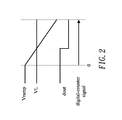
- FIG. 2 shows exemplary timing diagrams of pertinent signals of the comparator and the ADC of FIG. 1 ;
- FIG. 3 shows exemplary timing diagrams of pertinent signals of the DDS circuit according to one embodiment of the present invention.
- FIG. 4 shows exemplary timing diagrams of pertinent signals of the DDS circuit adopting a scheme different from the embodiment of the present invention as shown in FIG. 3 .
- FIG. 1 shows a circuit diagram illustrating a digital double-sampling (DDS) circuit 100 with dark-sun prevention scheme adaptable to a pixel circuit 11 of an image sensor, such as a complementary metal-oxide-semiconductor (CMOS) image sensor, according to one embodiment of the present invention.
- DDS digital double-sampling
- CMOS complementary metal-oxide-semiconductor
- FIG. 1 shows a circuit diagram illustrating a digital double-sampling (DDS) circuit 100 with dark-sun prevention scheme adaptable to a pixel circuit 11 of an image sensor, such as a complementary metal-oxide-semiconductor (CMOS) image sensor, according to one embodiment of the present invention.
- CMOS complementary metal-oxide-semiconductor
- the pixel circuit 11 may include a transfer transistor m 1 , a reset transistor m 2 , a source follower transistor m 3 and a row selection transistor m 4 , which may, for example, be implemented by N-type metal-oxide-semiconductor (NMOS) transistors.
- NMOS N-type metal-oxide-semiconductor
- FIG. 1 a photodiode PD is connected between the transfer transistor m 1 and ground.
- the transfer transistor m 1 is connected between a floating diffusion (FD) node and the photodiode PD, and a gate of the transfer transistor m 1 is connected to a transfer signal Tx.
- FD floating diffusion
- the reset transistor m 2 is connected between power VDD and the FD node, and a gate of the reset transistor m 2 is connected to a reset signal Rx.
- the source follower transistor m 3 and the row selection transistor m 4 are connected in series between the power VDD and an image output node VL, and gates of the source follower transistor m 3 and the row selection transistor m 4 are connected to the FD node and a selection signal SEL, respectively.
- a first bias transistor m 5 may be connected between the image output node VL and the ground, and a gate of the bias transistor m 5 is connected to a first bias voltage VB.
- the DDS circuit 100 of the embodiment may include a comparator 12 , which may, for example, be implemented by an operational amplifier. Specifically, a first input node (e.g., positive (+) input node) of the comparator 12 is connected to a ramp voltage Vramp, and a second input node (e.g., negative ( ⁇ ) input node VI) of the comparator 12 is connected to the image output node VL (of the pixel circuit 11 ) via a capacitor Ci.
- a first input node e.g., positive (+) input node
- Vramp a ramp voltage
- a second input node e.g., negative ( ⁇ ) input node VI
- a reset switch SW controlled by a reset enable signal rst_en is connected between the negative input node VI and the positive (+) input node of the comparator 12 for resetting the capacitor Ci disposed between the image output node VL the and (the negative ( ⁇ ) input node VI of) the comparator 12 .
- the DDS circuit 100 of the embodiment may include an analog-to-digital converter (ADC) 13 , which receives a comparison output dout of the comparator 12 , and accordingly generates a digital-counter signal, by a counter 131 that counts while the ramp voltage Vramp is ramping (down).
- the generated digital-counter signal represents an amount of time during which the comparison output dout is asserted (e.g., high level).
- FIG. 2 shows exemplary timing diagrams of pertinent signals of the comparator 12 and the ADC 13 of FIG. 1 .
- the counter 131 of the ADC 13 may use m bits to count from 0 to 2 m ⁇ 1 (e.g., 8-bit counter that counts from 0 to 255), and may generate a reset-ADC value.
- the counter 131 of the ADC 13 may use n bits (m and n are positive integers and m ⁇ n) to count from 0 to 2 n ⁇ 1 (e.g., 10-bit counter that counts from 0 to 1023) and may generate a signal-ADC value.
- the ADC 13 may include a memory 132 for temporarily storing the generated reset-ADC value and the generated signal-ADC value.
- the DDS circuit 100 of the embodiment may include a subtractor with digital-detection (subtractor hereinafter) 14 configured to subtract the reset-ADC value from the signal-ADC value, thereby resulting in a difference value representing a sampled output of the photodiode signal.
- a subtractor with digital-detection subtractor hereinafter
- an output of the subtractor 14 i.e., sampled output of the DDS circuit 100
- a maximum count i.e., 2 n ⁇ 1
- the DDS circuit 100 of the embodiment may include a clamp circuit 15 that is connected between the power VDD and the image output node VL.
- the clamp circuit 15 may include a clamp transistor m 6 (e.g., NMOS transistor) configured to generate (for example, at a source thereof) a clamp voltage at the image output node VL.
- a gate of the clamp transistor m 6 is controlled by a clamp enable signal bs_en. For example, when the clamp enable signal bs_en is asserted (e.g., high level), the clamp circuit 15 is enabled to generate the clamp voltage; otherwise, no clamp voltage is generated.
- the clamp circuit 15 may further include a second bias transistor m 7 that is connected between the power VDD and the clamp transistor m 6 , and a gate of the second bias transistor m 7 is connected to a second bias voltage vbs, where the second bias transistor m 7 and the clamp transistor m 6 are connected in series between the power VDD and the image output node VL.
- FIG. 3 shows exemplary timing diagrams of pertinent signals of the DDS circuit 100 according to one embodiment of the present invention. For better demonstrating aspect of the embodiment, only sun-light condition is shown. Specifically, in the reset phase (time period t 0 -t 6 ) of the digital double-sampling performed by the DDS circuit 100 , firstly the reset signal Rx, the reset enable signal rst_en and the clamp enable signal bs_en become asserted (e.g., high level) at time t 0 to reset the pixel circuit 11 , to reset the comparator 12 , and to enable the clamp circuit 15 , respectively.
- the reset phase time period t 0 -t 6
- the reset enable signal rst_en and the clamp enable signal bs_en become asserted (e.g., high level) at time t 0 to reset the pixel circuit 11 , to reset the comparator 12 , and to enable the clamp circuit 15 , respectively.
- the pixel circuit 11 finishes resetting when the reset signal Rx is de-asserted (e.g., low level). Accordingly, the image output node VL is clamped to the clamp voltage ⁇ V 1 (generated by the clamp circuit 15 ).
- the capacitor Ci finishes resetting (by the reset switch SW) when the reset enable signal rst_en is de-asserted (e.g., low level). Subsequently, at time t 3 , the clamp circuit 15 is disabled when the clamp enable signal bs_en is de-asserted (e.g., low level). Therefore, the image output node VL is no longer clamped. Moreover, the image output node VL drops to 0 volt due to sun-light condition.
- the ramp voltage Vramp is ramping (down) with an amount of ⁇ V 2 while the counter 131 of the ADC 13 counts from 0 to N 1 (i.e., 2 m ⁇ 1), and the reset-ADC value is thus generated (by the ADC 13 ).
- the clamp circuit 15 is disabled (at t 3 ) after the capacitor Ci finishes resetting (at t 2 ) but before the ramp voltage Vramp begins ramping (at t 4 ).
- the transfer transistor m 1 becomes enabled at time t 6 to transfer image signal from the photodiode PD to the FD node.
- the ramp voltage Vramp is ramping (down) with an amount of ⁇ V 3 while the counter 131 of the ADC 13 counts from 0 to N 2 (i.e., 2 n ⁇ 1), and the signal-ADC value is thus generated (by the ADC 13 ).
- ⁇ V 2 is about 20% of ⁇ V 3
- N 1 /N 2 may be 255/1023 in case of 10-bit ADC resolution.
- FIG. 4 shows exemplary timing diagrams of pertinent signals of the DDS circuit 100 adopting a scheme different from the embodiment of the present invention as shown in FIG. 3 , and only sun-light condition is shown.
- the clamp circuit 15 is enabled (with asserted clamp enable signal bs_en) until the end of the reset phase. Accordingly, the image output node VL is clamped at a certain level during the reset phase.
- the clamp circuit 15 may be turned on slightly, an output current I 1 (of the clamp circuit 15 ) thus flows toward the image output node VL.
- This output current I 1 makes the output current I 2 of the row selection transistor m 4 reduced and affects the signal transfer from the photodiode PD to the image output node VL during the reset phase in case of no sun-light or low-light condition. Accordingly, column fixed pattern noise (CFPN) may occur due to threshold voltage difference between the clamp transistor m 6 and the second bias transistor m 7 (of the clamp circuit 15 ).
- CFPN column fixed pattern noise
Abstract
A digital double-sampling (DDS) circuit includes a comparator with input nodes respectively connected to a ramp voltage and an image output node of a pixel circuit via a capacitor; a reset switch connected between the input nodes for resetting the capacitor; an analog-to-digital converter (ADC) coupled to receive a comparison output of the comparator, the ADC including a counter that counts while the ramp voltage is ramping, thereby generating a reset-ADC value in a reset phase and generating a signal-ADC value in a signal phase; a subtractor that subtracts the reset-ADC value from the signal-ADC value, thereby resulting in a difference value representing a sampled output; and a clamp circuit that generates a clamp voltage at the image output node. In the reset phase, the clamp circuit is disabled after the capacitor finishes resetting but before the ramp voltage begins ramping.
Description
The present invention generally relates to digital double sampling (DDS), and more particularly to a DDS circuit with dark-sun prevention scheme adaptable to an image sensor.
Digital double sampling (DDS) is a scheme commonly used to cancel read-out path offset and comparator delay variation when reading out photodiode information of an image sensor such as a complementary metal-oxide-semiconductor (CMOS) image sensor.
When taking a picture of sun light, the sun image may ordinarily become dark due to electron overflow of the photodiode. A clamp scheme is thus proposed to clamp an image output node of a pixel circuit at a certain level during the reset phase. However, the clamp scheme may disadvantageously affect the signal transfer from the photodiode to the image output node during the reset phase in case of no sun-light or low-light condition, and column fixed pattern noise (CFPN) may therefore occur.
For the reason that conventional clamp scheme could not effectively solve the sun-light phenomenon in the DDS system, a need has thus arisen to propose a novel scheme to overcome drawbacks of the conventional DDS system.
In view of the foregoing, it is an object of the embodiment of the present invention to provide a digital double-sampling (DDS) circuit capable of preventing dark-sun condition and column fixed pattern noise (CFPN).
According to one embodiment, a digital double-sampling (DDS) circuit includes a pixel circuit of an image sensor, a comparator, a reset switch, an analog-to-digital converter (ADC), a subtractor and a clamp circuit. The comparator has a first input node connected to a ramp voltage and a second input node connected to an image output node of the pixel circuit via a capacitor. The reset switch is connected between the first input node and the second input node for resetting the capacitor. The ADC is coupled to receive a comparison output of the comparator, the ADC including a counter that counts while the ramp voltage is ramping, thereby generating a reset-ADC value in a reset phase and generating a signal-ADC value in a signal phase. The subtractor subtracts the reset-ADC value from the signal-ADC value, thereby resulting in a difference value representing a sampled output. The clamp circuit generates a clamp voltage at the image output node. In the reset phase, the clamp circuit is disabled after the capacitor finishes resetting but before the ramp voltage begins ramping.
Specifically, the pixel circuit 11 may include a transfer transistor m1, a reset transistor m2, a source follower transistor m3 and a row selection transistor m4, which may, for example, be implemented by N-type metal-oxide-semiconductor (NMOS) transistors. As exemplified in FIG. 1 , a photodiode PD is connected between the transfer transistor m1 and ground. The transfer transistor m1 is connected between a floating diffusion (FD) node and the photodiode PD, and a gate of the transfer transistor m1 is connected to a transfer signal Tx. The reset transistor m2 is connected between power VDD and the FD node, and a gate of the reset transistor m2 is connected to a reset signal Rx. The source follower transistor m3 and the row selection transistor m4 are connected in series between the power VDD and an image output node VL, and gates of the source follower transistor m3 and the row selection transistor m4 are connected to the FD node and a selection signal SEL, respectively. A first bias transistor m5 may be connected between the image output node VL and the ground, and a gate of the bias transistor m5 is connected to a first bias voltage VB.
The DDS circuit 100 of the embodiment may include a comparator 12, which may, for example, be implemented by an operational amplifier. Specifically, a first input node (e.g., positive (+) input node) of the comparator 12 is connected to a ramp voltage Vramp, and a second input node (e.g., negative (−) input node VI) of the comparator 12 is connected to the image output node VL (of the pixel circuit 11) via a capacitor Ci. A reset switch SW, controlled by a reset enable signal rst_en is connected between the negative input node VI and the positive (+) input node of the comparator 12 for resetting the capacitor Ci disposed between the image output node VL the and (the negative (−) input node VI of) the comparator 12.
The DDS circuit 100 of the embodiment may include an analog-to-digital converter (ADC) 13, which receives a comparison output dout of the comparator 12, and accordingly generates a digital-counter signal, by a counter 131 that counts while the ramp voltage Vramp is ramping (down). The generated digital-counter signal represents an amount of time during which the comparison output dout is asserted (e.g., high level). FIG. 2 shows exemplary timing diagrams of pertinent signals of the comparator 12 and the ADC 13 of FIG. 1 . In a reset phase of the digital double-sampling performed by the DDS circuit 100, the counter 131 of the ADC 13 may use m bits to count from 0 to 2m−1 (e.g., 8-bit counter that counts from 0 to 255), and may generate a reset-ADC value. On the other hand, in a signal phase of the digital double-sampling performed by the DDS circuit 100, the counter 131 of the ADC 13 may use n bits (m and n are positive integers and m≤n) to count from 0 to 2n−1 (e.g., 10-bit counter that counts from 0 to 1023) and may generate a signal-ADC value. It is noted that the ADC 13 may include a memory 132 for temporarily storing the generated reset-ADC value and the generated signal-ADC value.
The DDS circuit 100 of the embodiment may include a subtractor with digital-detection (subtractor hereinafter) 14 configured to subtract the reset-ADC value from the signal-ADC value, thereby resulting in a difference value representing a sampled output of the photodiode signal. In the embodiment, if the reset-ADC value is equal to a maximum count (i.e., 2m−1) of the reset phase, indicating a sun-light condition, an output of the subtractor 14 (i.e., sampled output of the DDS circuit 100) is then set to a maximum count (i.e., 2n−1) of the signal phase, thereby preventing dark-sun result; otherwise the difference value is outputted as the sampled output.
The DDS circuit 100 of the embodiment may include a clamp circuit 15 that is connected between the power VDD and the image output node VL. In the embodiment, the clamp circuit 15 may include a clamp transistor m6 (e.g., NMOS transistor) configured to generate (for example, at a source thereof) a clamp voltage at the image output node VL. A gate of the clamp transistor m6 is controlled by a clamp enable signal bs_en. For example, when the clamp enable signal bs_en is asserted (e.g., high level), the clamp circuit 15 is enabled to generate the clamp voltage; otherwise, no clamp voltage is generated. The clamp circuit 15 may further include a second bias transistor m7 that is connected between the power VDD and the clamp transistor m6, and a gate of the second bias transistor m7 is connected to a second bias voltage vbs, where the second bias transistor m7 and the clamp transistor m6 are connected in series between the power VDD and the image output node VL.
At time t2, the capacitor Ci finishes resetting (by the reset switch SW) when the reset enable signal rst_en is de-asserted (e.g., low level). Subsequently, at time t3, the clamp circuit 15 is disabled when the clamp enable signal bs_en is de-asserted (e.g., low level). Therefore, the image output node VL is no longer clamped. Moreover, the image output node VL drops to 0 volt due to sun-light condition. Afterward, from time t4 to t5, the ramp voltage Vramp is ramping (down) with an amount of Δ V2 while the counter 131 of the ADC 13 counts from 0 to N1 (i.e., 2m−1), and the reset-ADC value is thus generated (by the ADC 13). According to one aspect of the embodiment, in the reset phase, the clamp circuit 15 is disabled (at t3) after the capacitor Ci finishes resetting (at t2) but before the ramp voltage Vramp begins ramping (at t4).
In the signal phase (time period t6-t8) of the digital double-sampling performed by the DDS circuit 100, firstly the transfer transistor m1 becomes enabled at time t6 to transfer image signal from the photodiode PD to the FD node. Afterward, from time t7 to t8, the ramp voltage Vramp is ramping (down) with an amount of Δ V3 while the counter 131 of the ADC 13 counts from 0 to N2 (i.e., 2n−1), and the signal-ADC value is thus generated (by the ADC 13). In one exemplary embodiment, Δ V2 is about 20% of Δ V3, and N1/N2 may be 255/1023 in case of 10-bit ADC resolution.
According to the embodiment set forth above, in the reset phase (particularly during time period t3-t6), as the clamp circuit 15 is disabled, no output current I1 (of the clamp circuit 15) flows toward the image output node VL due to unexpectedly turning on the clamp circuit 15. Accordingly, the output current I2 of the row selection transistor m4 would not be affected (e.g., be decreased), particularly in case of no sun-light or low-light condition, and column fixed pattern noise (CFPN) would not occur due to threshold voltage difference between the clamp transistor m6 and the second bias transistor m7 (of the clamp circuit 15).
Although specific embodiments have been illustrated and described, it will be appreciated by those skilled in the art that various modifications may be made without departing from the scope of the present invention, which is intended to be limited solely by the appended claims.
Claims (11)
1. A digital double-sampling (DDS) circuit, comprising:
a pixel circuit of an image sensor;
a comparator with a first input node connected to a ramp voltage and a second input node connected to an image output node of the pixel circuit via a capacitor;
a reset switch connected between the first input node and the second input node for resetting the capacitor;
an analog-to-digital converter (ADC) coupled to receive a comparison output of the comparator, the ADC including a counter that counts while the ramp voltage is ramping, thereby generating a reset-ADC value in a reset phase and generating a signal-ADC value in a signal phase;
a subtractor that subtracts the reset-ADC value from the signal-ADC value, thereby resulting in a difference value representing a sampled output; and
a clamp circuit that generates a clamp voltage at the image output node;
wherein, in the reset phase, the clamp circuit is disabled after the capacitor finishes resetting but before the ramp voltage begins ramping;
wherein the following steps are performed in sequence in the reset phase:
resetting the pixel circuit, resetting the capacitor and enabling the clamp circuit, respectively;
stopping resetting the pixel circuit, thereby clamping the image output node to the clamp voltage;
stopping resetting the capacitor;
disabling the clamp circuit, thereby no longer clamping the image output node to the clamp voltage; and
ramping down the ramp voltage while the counter counts, thereby generating the reset-ADC value.
2. The DDS circuit of claim 1 , wherein the comparator comprises an operational amplifier with a positive input node acting as the first input node, and a negative input node acting as the second input node.
3. The DDS circuit of claim 1 , wherein the ADC comprises a memory that temporarily stores the reset-ADC value and the signal-ADC value.
4. The DDS circuit of claim 1 , wherein the subtractor sets the sampled output to a maximum count of the counter of the signal phase, when the reset-ADC value is equal to a maximum count of the counter of the reset phase.
5. The DDS circuit of claim 4 , wherein the subtractor outputs the difference value as the sampled output, when the reset-ADC value is less than the maximum count of the counter of the reset phase.
6. The DDS circuit of claim 5 , wherein the counter counts from 0 to 2m−1 in the reset phase, and the counter counts from 0 to 2n−1 in the signal phase, wherein m and n are positive integers, and m is less than or equal to n.
7. The DDS circuit of claim 1 , wherein the clamp circuit comprises:
a clamp transistor that generates the clamp voltage at the image output node; and
a bias transistor connected between a power and the clamp transistor;
wherein the bias transistor and the clamp transistor are connected in series between a power and the image output node.
8. The DDS circuit of claim 7 , wherein a gate of the clamp transistor is controlled by a clamp enable signal, and a gate of the second bias transistor is connected to a bias voltage.
9. The DDS circuit of claim 1 , performing the following steps in sequence in the signal phase:
transferring image signal from a photodiode of the pixel circuit to a floating diffusion (FD) node of the pixel circuit; and
ramping down the ramp voltage while the counter counts, thereby generating the signal-ADC value.
10. The DDS circuit of claim 1 , wherein the pixel circuit comprises:
a photodiode;
a transfer transistor connected between a floating diffusion (FD) node and the photodiode, a gate of the transfer transistor being connected to a transfer signal;
a reset transistor connected between a power and the FD node, a gate of the reset transistor being connected to a reset signal;
a source follower transistor; and
a row selection transistor, the source follower transistor and the row selection transistor being connected in series between the power and the image output node, gates of the source follower transistor and the row selection transistor being connected to the FD node and a selection signal, respectively.
11. The DDS circuit of claim 10 , further comprising:
a bias transistor connected between the image output node and ground, a gate of the bias transistor being connected to a bias voltage.
Priority Applications (1)
| Application Number | Priority Date | Filing Date | Title |
|---|---|---|---|
| US16/178,381 US10498989B1 (en) | 2018-11-01 | 2018-11-01 | Digital double sampling circuit |
Applications Claiming Priority (1)
| Application Number | Priority Date | Filing Date | Title |
|---|---|---|---|
| US16/178,381 US10498989B1 (en) | 2018-11-01 | 2018-11-01 | Digital double sampling circuit |
Publications (1)
| Publication Number | Publication Date |
|---|---|
| US10498989B1 true US10498989B1 (en) | 2019-12-03 |
Family
ID=68695999
Family Applications (1)
| Application Number | Title | Priority Date | Filing Date |
|---|---|---|---|
| US16/178,381 Active US10498989B1 (en) | 2018-11-01 | 2018-11-01 | Digital double sampling circuit |
Country Status (1)
| Country | Link |
|---|---|
| US (1) | US10498989B1 (en) |
Cited By (3)
| Publication number | Priority date | Publication date | Assignee | Title |
|---|---|---|---|---|
| WO2023044081A1 (en) * | 2021-09-17 | 2023-03-23 | Varex Imaging Corporation | Imaging system with noise reduction |
| US11750944B2 (en) | 2021-05-28 | 2023-09-05 | Varex Imaging Corporation | Pixel noise cancellation system |
| US11812187B2 (en) | 2021-05-28 | 2023-11-07 | Varex Imaging Corporation | Combined imaging array and strip |
Citations (15)
| Publication number | Priority date | Publication date | Assignee | Title |
|---|---|---|---|---|
| US5332931A (en) * | 1991-06-24 | 1994-07-26 | Harris Corporation | High speed differential comparator |
| US5781312A (en) * | 1994-12-16 | 1998-07-14 | Fuji Xerox, Co. Ltd. | Image input method and apparatus |
| US20040027471A1 (en) * | 2002-05-30 | 2004-02-12 | Ken Koseki | Captured-image-signal processing method and apparatus and imaging apparatus |
| US20040080637A1 (en) * | 2002-06-11 | 2004-04-29 | Nobuo Nakamura | Solid-state image pickup device and control method thereof |
| US20060001750A1 (en) * | 2004-07-02 | 2006-01-05 | Fujitsu Limited | Differential comparator, analog/digital conversion apparatus and imaging apparatus |
| US20090167585A1 (en) * | 2007-12-29 | 2009-07-02 | Hyun Soo Yeom | Analog reference voltage generator, method thereof, analog-to-digital converter including the same, and image sensor including the same |
| US20110013050A1 (en) * | 2009-07-14 | 2011-01-20 | Sony Corporation | Solid-state imaging device, control method therefor, and camera system |
| US7948540B2 (en) * | 2006-09-07 | 2011-05-24 | Canon Kabushiki Kaisha | Photoelectric conversion device with isolation switches arranged between signal lines and amplifiers |
| US20150249797A1 (en) * | 2012-10-25 | 2015-09-03 | Sharp Kabushiki Kaisha | Solid-state imaging device |
| US20160006961A1 (en) * | 2014-07-04 | 2016-01-07 | Naoki ASABA | Photoelectric conversion element, image reading device, image forming apparatus, and signal control method |
| US9264643B1 (en) * | 2012-12-29 | 2016-02-16 | Rambus, Inc. | Methods and circuitries for pixel sampling |
| US20160165166A1 (en) * | 2014-12-05 | 2016-06-09 | Kyoung Min Koh | Image sensor for improving nonlinearity of row code region, and device including the same |
| US20160219234A1 (en) * | 2012-12-20 | 2016-07-28 | Sony Corporation | Imaging device, imaging apparatus, electronic apparatus, threshold value calculation apparatus, and imaging method |
| US20170201700A1 (en) * | 2016-01-12 | 2017-07-13 | Hideki Hashimoto | Photoelectric conversion element, image reading device, image forming apparatus, image reading method, and computer-readable recording medium |
| US20190115931A1 (en) * | 2016-06-10 | 2019-04-18 | Jonathan Ephraim David Hurwitz | Multi-stage conversion analog-to-digital converter |
-
2018
- 2018-11-01 US US16/178,381 patent/US10498989B1/en active Active
Patent Citations (16)
| Publication number | Priority date | Publication date | Assignee | Title |
|---|---|---|---|---|
| US5332931A (en) * | 1991-06-24 | 1994-07-26 | Harris Corporation | High speed differential comparator |
| US5781312A (en) * | 1994-12-16 | 1998-07-14 | Fuji Xerox, Co. Ltd. | Image input method and apparatus |
| US20040027471A1 (en) * | 2002-05-30 | 2004-02-12 | Ken Koseki | Captured-image-signal processing method and apparatus and imaging apparatus |
| US20040080637A1 (en) * | 2002-06-11 | 2004-04-29 | Nobuo Nakamura | Solid-state image pickup device and control method thereof |
| US20060001750A1 (en) * | 2004-07-02 | 2006-01-05 | Fujitsu Limited | Differential comparator, analog/digital conversion apparatus and imaging apparatus |
| US7145494B2 (en) * | 2004-07-02 | 2006-12-05 | Fujitsu Limited | Differential comparator, analog/digital conversion apparatus and imaging apparatus |
| US7948540B2 (en) * | 2006-09-07 | 2011-05-24 | Canon Kabushiki Kaisha | Photoelectric conversion device with isolation switches arranged between signal lines and amplifiers |
| US20090167585A1 (en) * | 2007-12-29 | 2009-07-02 | Hyun Soo Yeom | Analog reference voltage generator, method thereof, analog-to-digital converter including the same, and image sensor including the same |
| US20110013050A1 (en) * | 2009-07-14 | 2011-01-20 | Sony Corporation | Solid-state imaging device, control method therefor, and camera system |
| US20150249797A1 (en) * | 2012-10-25 | 2015-09-03 | Sharp Kabushiki Kaisha | Solid-state imaging device |
| US20160219234A1 (en) * | 2012-12-20 | 2016-07-28 | Sony Corporation | Imaging device, imaging apparatus, electronic apparatus, threshold value calculation apparatus, and imaging method |
| US9264643B1 (en) * | 2012-12-29 | 2016-02-16 | Rambus, Inc. | Methods and circuitries for pixel sampling |
| US20160006961A1 (en) * | 2014-07-04 | 2016-01-07 | Naoki ASABA | Photoelectric conversion element, image reading device, image forming apparatus, and signal control method |
| US20160165166A1 (en) * | 2014-12-05 | 2016-06-09 | Kyoung Min Koh | Image sensor for improving nonlinearity of row code region, and device including the same |
| US20170201700A1 (en) * | 2016-01-12 | 2017-07-13 | Hideki Hashimoto | Photoelectric conversion element, image reading device, image forming apparatus, image reading method, and computer-readable recording medium |
| US20190115931A1 (en) * | 2016-06-10 | 2019-04-18 | Jonathan Ephraim David Hurwitz | Multi-stage conversion analog-to-digital converter |
Cited By (3)
| Publication number | Priority date | Publication date | Assignee | Title |
|---|---|---|---|---|
| US11750944B2 (en) | 2021-05-28 | 2023-09-05 | Varex Imaging Corporation | Pixel noise cancellation system |
| US11812187B2 (en) | 2021-05-28 | 2023-11-07 | Varex Imaging Corporation | Combined imaging array and strip |
| WO2023044081A1 (en) * | 2021-09-17 | 2023-03-23 | Varex Imaging Corporation | Imaging system with noise reduction |
Similar Documents
| Publication | Publication Date | Title |
|---|---|---|
| US8358360B2 (en) | Solid-state image sensor device having signal noise reduction circuitry | |
| US7538709B2 (en) | Analog-to-digital conversion method, analog-to-digital converter, semiconductor device for detecting distribution of physical quantity, and electronic apparatus | |
| US8785832B2 (en) | Solid-state imaging apparatus having a comparator comparing a generated reference signal with an analog signal from a pixel and its driving method | |
| US10382707B2 (en) | Imaging device | |
| US8963759B2 (en) | Imaging systems with per-column analog-to-digital converter non-linearity correction capabilities | |
| US20110194007A1 (en) | Cmos image sensor | |
| US20080111059A1 (en) | Digital double sampling method, a related cmos image sensor, and a digital camera comprising the cmos image sensor | |
| US20120008032A1 (en) | Solid-state imaging apparatus | |
| US10498989B1 (en) | Digital double sampling circuit | |
| US8319850B2 (en) | Imaging element with signal holding section, drive method for imaging element with signal holding period, and camera with imaging element and signal holding section | |
| US20120006973A1 (en) | Image sensor with sample and hold circuitry for addressing time variant noise | |
| US10257451B2 (en) | Comparison device and CMOS image sensor using the same | |
| US10574917B2 (en) | Pixel output level control device and CMOS image sensor using the same | |
| US10582138B2 (en) | Image sensors with dual conversion gain pixels and anti-eclipse circuitry | |
| US10104321B1 (en) | Image processing system and method for an image sensor | |
| US10811448B2 (en) | Solid-state imaging device | |
| US8134769B2 (en) | Imaging apparatus | |
| KR102469101B1 (en) | Pixel Power Noise Cancelation Apparatus, and CMOS Image Sensor Using That | |
| US20120199723A1 (en) | Solid-state imaging device | |
| US8106975B2 (en) | Analog dark average circuit and method for an image sensor | |
| TWI702848B (en) | Digital double sampling circuit | |
| US9973717B1 (en) | Image sensors with anti-eclipse circuitry | |
| CN111343397B (en) | Digital double sampling circuit | |
| TWI678108B (en) | Image processing system and method for an image sensor | |
| US8558160B2 (en) | CMOS imager with companded column signals |
Legal Events
| Date | Code | Title | Description |
|---|---|---|---|
| FEPP | Fee payment procedure |
Free format text: ENTITY STATUS SET TO UNDISCOUNTED (ORIGINAL EVENT CODE: BIG.); ENTITY STATUS OF PATENT OWNER: LARGE ENTITY |
|
| STCF | Information on status: patent grant |
Free format text: PATENTED CASE |
|
| MAFP | Maintenance fee payment |
Free format text: PAYMENT OF MAINTENANCE FEE, 4TH YEAR, LARGE ENTITY (ORIGINAL EVENT CODE: M1551); ENTITY STATUS OF PATENT OWNER: LARGE ENTITY Year of fee payment: 4 |