US10470299B2 - Power signal transmission structure and design method thereof - Google Patents
Power signal transmission structure and design method thereof Download PDFInfo
- Publication number
- US10470299B2 US10470299B2 US15/934,897 US201815934897A US10470299B2 US 10470299 B2 US10470299 B2 US 10470299B2 US 201815934897 A US201815934897 A US 201815934897A US 10470299 B2 US10470299 B2 US 10470299B2
- Authority
- US
- United States
- Prior art keywords
- vias
- power
- power signal
- transmission structure
- signal transmission
- Prior art date
- Legal status (The legal status is an assumption and is not a legal conclusion. Google has not performed a legal analysis and makes no representation as to the accuracy of the status listed.)
- Active
Links
Images


Classifications
-
- H—ELECTRICITY
- H05—ELECTRIC TECHNIQUES NOT OTHERWISE PROVIDED FOR
- H05K—PRINTED CIRCUITS; CASINGS OR CONSTRUCTIONAL DETAILS OF ELECTRIC APPARATUS; MANUFACTURE OF ASSEMBLAGES OF ELECTRICAL COMPONENTS
- H05K1/00—Printed circuits
- H05K1/02—Details
- H05K1/0213—Electrical arrangements not otherwise provided for
- H05K1/0263—High current adaptations, e.g. printed high current conductors or using auxiliary non-printed means; Fine and coarse circuit patterns on one circuit board
- H05K1/0265—High current adaptations, e.g. printed high current conductors or using auxiliary non-printed means; Fine and coarse circuit patterns on one circuit board characterized by the lay-out of or details of the printed conductors, e.g. reinforced conductors, redundant conductors, conductors having different cross-sections
-
- H—ELECTRICITY
- H05—ELECTRIC TECHNIQUES NOT OTHERWISE PROVIDED FOR
- H05K—PRINTED CIRCUITS; CASINGS OR CONSTRUCTIONAL DETAILS OF ELECTRIC APPARATUS; MANUFACTURE OF ASSEMBLAGES OF ELECTRICAL COMPONENTS
- H05K1/00—Printed circuits
- H05K1/02—Details
- H05K1/11—Printed elements for providing electric connections to or between printed circuits
- H05K1/111—Pads for surface mounting, e.g. lay-out
- H05K1/112—Pads for surface mounting, e.g. lay-out directly combined with via connections
- H05K1/114—Pad being close to via, but not surrounding the via
-
- H—ELECTRICITY
- H05—ELECTRIC TECHNIQUES NOT OTHERWISE PROVIDED FOR
- H05K—PRINTED CIRCUITS; CASINGS OR CONSTRUCTIONAL DETAILS OF ELECTRIC APPARATUS; MANUFACTURE OF ASSEMBLAGES OF ELECTRICAL COMPONENTS
- H05K1/00—Printed circuits
- H05K1/02—Details
- H05K1/11—Printed elements for providing electric connections to or between printed circuits
- H05K1/115—Via connections; Lands around holes or via connections
- H05K1/116—Lands, clearance holes or other lay-out details concerning the surrounding of a via
-
- H—ELECTRICITY
- H05—ELECTRIC TECHNIQUES NOT OTHERWISE PROVIDED FOR
- H05K—PRINTED CIRCUITS; CASINGS OR CONSTRUCTIONAL DETAILS OF ELECTRIC APPARATUS; MANUFACTURE OF ASSEMBLAGES OF ELECTRICAL COMPONENTS
- H05K2201/00—Indexing scheme relating to printed circuits covered by H05K1/00
- H05K2201/09—Shape and layout
- H05K2201/09209—Shape and layout details of conductors
- H05K2201/09218—Conductive traces
- H05K2201/09254—Branched layout
-
- H—ELECTRICITY
- H05—ELECTRIC TECHNIQUES NOT OTHERWISE PROVIDED FOR
- H05K—PRINTED CIRCUITS; CASINGS OR CONSTRUCTIONAL DETAILS OF ELECTRIC APPARATUS; MANUFACTURE OF ASSEMBLAGES OF ELECTRICAL COMPONENTS
- H05K2201/00—Indexing scheme relating to printed circuits covered by H05K1/00
- H05K2201/09—Shape and layout
- H05K2201/09209—Shape and layout details of conductors
- H05K2201/0929—Conductive planes
- H05K2201/093—Layout of power planes, ground planes or power supply conductors, e.g. having special clearance holes therein
-
- H—ELECTRICITY
- H05—ELECTRIC TECHNIQUES NOT OTHERWISE PROVIDED FOR
- H05K—PRINTED CIRCUITS; CASINGS OR CONSTRUCTIONAL DETAILS OF ELECTRIC APPARATUS; MANUFACTURE OF ASSEMBLAGES OF ELECTRICAL COMPONENTS
- H05K2201/00—Indexing scheme relating to printed circuits covered by H05K1/00
- H05K2201/09—Shape and layout
- H05K2201/09209—Shape and layout details of conductors
- H05K2201/0929—Conductive planes
- H05K2201/09309—Core having two or more power planes; Capacitive laminate of two power planes
-
- H—ELECTRICITY
- H05—ELECTRIC TECHNIQUES NOT OTHERWISE PROVIDED FOR
- H05K—PRINTED CIRCUITS; CASINGS OR CONSTRUCTIONAL DETAILS OF ELECTRIC APPARATUS; MANUFACTURE OF ASSEMBLAGES OF ELECTRICAL COMPONENTS
- H05K2201/00—Indexing scheme relating to printed circuits covered by H05K1/00
- H05K2201/09—Shape and layout
- H05K2201/09209—Shape and layout details of conductors
- H05K2201/09372—Pads and lands
- H05K2201/09409—Multiple rows of pads, lands, terminals or dummy patterns; Multiple rows of mounted components
-
- H—ELECTRICITY
- H05—ELECTRIC TECHNIQUES NOT OTHERWISE PROVIDED FOR
- H05K—PRINTED CIRCUITS; CASINGS OR CONSTRUCTIONAL DETAILS OF ELECTRIC APPARATUS; MANUFACTURE OF ASSEMBLAGES OF ELECTRICAL COMPONENTS
- H05K2201/00—Indexing scheme relating to printed circuits covered by H05K1/00
- H05K2201/09—Shape and layout
- H05K2201/09209—Shape and layout details of conductors
- H05K2201/09372—Pads and lands
- H05K2201/09427—Special relation between the location or dimension of a pad or land and the location or dimension of a terminal
-
- H—ELECTRICITY
- H05—ELECTRIC TECHNIQUES NOT OTHERWISE PROVIDED FOR
- H05K—PRINTED CIRCUITS; CASINGS OR CONSTRUCTIONAL DETAILS OF ELECTRIC APPARATUS; MANUFACTURE OF ASSEMBLAGES OF ELECTRICAL COMPONENTS
- H05K2201/00—Indexing scheme relating to printed circuits covered by H05K1/00
- H05K2201/09—Shape and layout
- H05K2201/09209—Shape and layout details of conductors
- H05K2201/09372—Pads and lands
- H05K2201/09463—Partial lands, i.e. lands or conductive rings not completely surrounding the hole
-
- H—ELECTRICITY
- H05—ELECTRIC TECHNIQUES NOT OTHERWISE PROVIDED FOR
- H05K—PRINTED CIRCUITS; CASINGS OR CONSTRUCTIONAL DETAILS OF ELECTRIC APPARATUS; MANUFACTURE OF ASSEMBLAGES OF ELECTRICAL COMPONENTS
- H05K2201/00—Indexing scheme relating to printed circuits covered by H05K1/00
- H05K2201/09—Shape and layout
- H05K2201/09209—Shape and layout details of conductors
- H05K2201/095—Conductive through-holes or vias
- H05K2201/09609—Via grid, i.e. two-dimensional array of vias or holes in a single plane
-
- H—ELECTRICITY
- H05—ELECTRIC TECHNIQUES NOT OTHERWISE PROVIDED FOR
- H05K—PRINTED CIRCUITS; CASINGS OR CONSTRUCTIONAL DETAILS OF ELECTRIC APPARATUS; MANUFACTURE OF ASSEMBLAGES OF ELECTRICAL COMPONENTS
- H05K2201/00—Indexing scheme relating to printed circuits covered by H05K1/00
- H05K2201/09—Shape and layout
- H05K2201/09209—Shape and layout details of conductors
- H05K2201/095—Conductive through-holes or vias
- H05K2201/09618—Via fence, i.e. one-dimensional array of vias
-
- H—ELECTRICITY
- H05—ELECTRIC TECHNIQUES NOT OTHERWISE PROVIDED FOR
- H05K—PRINTED CIRCUITS; CASINGS OR CONSTRUCTIONAL DETAILS OF ELECTRIC APPARATUS; MANUFACTURE OF ASSEMBLAGES OF ELECTRICAL COMPONENTS
- H05K2201/00—Indexing scheme relating to printed circuits covered by H05K1/00
- H05K2201/09—Shape and layout
- H05K2201/09209—Shape and layout details of conductors
- H05K2201/09654—Shape and layout details of conductors covering at least two types of conductors provided for in H05K2201/09218 - H05K2201/095
- H05K2201/0969—Apertured conductors
-
- H—ELECTRICITY
- H05—ELECTRIC TECHNIQUES NOT OTHERWISE PROVIDED FOR
- H05K—PRINTED CIRCUITS; CASINGS OR CONSTRUCTIONAL DETAILS OF ELECTRIC APPARATUS; MANUFACTURE OF ASSEMBLAGES OF ELECTRICAL COMPONENTS
- H05K2201/00—Indexing scheme relating to printed circuits covered by H05K1/00
- H05K2201/09—Shape and layout
- H05K2201/09209—Shape and layout details of conductors
- H05K2201/09654—Shape and layout details of conductors covering at least two types of conductors provided for in H05K2201/09218 - H05K2201/095
- H05K2201/09709—Staggered pads, lands or terminals; Parallel conductors in different planes
-
- H—ELECTRICITY
- H05—ELECTRIC TECHNIQUES NOT OTHERWISE PROVIDED FOR
- H05K—PRINTED CIRCUITS; CASINGS OR CONSTRUCTIONAL DETAILS OF ELECTRIC APPARATUS; MANUFACTURE OF ASSEMBLAGES OF ELECTRICAL COMPONENTS
- H05K2201/00—Indexing scheme relating to printed circuits covered by H05K1/00
- H05K2201/09—Shape and layout
- H05K2201/09209—Shape and layout details of conductors
- H05K2201/09654—Shape and layout details of conductors covering at least two types of conductors provided for in H05K2201/09218 - H05K2201/095
- H05K2201/0979—Redundant conductors or connections, i.e. more than one current path between two points
Definitions
- the invention relates to a signal transmission structure, and particularly relates to a power signal transmission structure and a design method thereof.
- circuit layers in circuit boards used in the electronic products have been increased from one or two layers to six layers, eight layers, or even more than ten layers. Accordingly, electronic devices can be more densely mounted on the circuit boards.
- vias are configured on circuits, so that electrodes on respective layers of the circuit board are electrically connected correspondingly. In other words, horizontal signals are converted into vertical ones through the vias to be transmitted to another layer in the circuit board.
- a power electrode if a power signal is transmitted through a single via, the single via may generate heat due to currents flowing through.
- the conductor in the via when a via overheats, the conductor in the via may be damaged due to the high temperature, and devices on the circuit board may be unable to function normally or even be burned out.
- a thicker power wire may be adopted, or more vias may be disposed to increase the volume of the conductor transmitting the power signal, so as to share the current on the transmission path of the power signals.
- the current may take the shortest and closest path so some vias do not work as expected, and the current partaking of the multiple vias is affected.
- One or some embodiments of the invention provide a power signal transmission structure and a design method of the power signal transmission structure capable of facilitating current sharing by multiple vias.
- the power supply signal transmission structure is adapted for a circuit board having a first surface and a second surface opposite to the first surface, and the power signal transmission structure includes a first power electrode, a second power electrode, and a plurality of vias.
- the first power electrode is disposed on the first surface and has a plurality of power pad regions for receiving a power signal.
- the second power electrode is disposed on the second surface.
- the vias penetrate the circuit board to electrically connect the first power electrode and the second power electrode.
- the vias are arranged in accordance with the current direction of the power signal to balance the current received by the vias.
- a design method of the power signal transmission structure includes the following.
- a current direction of the power signal received by a first power electrode through a plurality of power pad regions is detected.
- the first power electrode is disposed on a first surface of a circuit board.
- a plurality of vias is disposed based on the current direction of the power signal to balance the current received by the vias.
- the vias penetrate the circuit board to electrically connect the first power electrode and a second power electrode disposed on a second surface of the circuit board opposite to the first surface.
- the power supply signal transmission structure is adapted for a circuit board having a first surface and a second surface opposite to the first surface.
- the power signal transmission structure includes a first power electrode, a second power electrode, a plurality of vias, and a plurality of first conductor isolation rings.
- the first power electrode is disposed on the first surface and has a plurality of power pad regions for receiving a power signal.
- the second power electrode is disposed on the second surface.
- the vias penetrate the circuit board to electrically connect the first power electrode and the second power electrode.
- a plurality of first conductor isolation rings is disposed to the first power electrode. The first conductor isolation rings surround some of the vias based on the current direction of the power signal to balance the current received by the vias.
- a design method of the power signal transmission structure includes the following.
- a current direction of the power signal received by a first power electrode through a plurality of power pad regions is detected.
- the first electrode is disposed on a first surface of a circuit board.
- a plurality of vias is disposed. The vias penetrate the circuit board to electrically connect the first power electrode and a second power electrode disposed on a second surface of the circuit board opposite to the first surface.
- a plurality of first conductor isolation rings is disposed to the first power electrode based on the current direction of the power signal. The first conductor isolation rings surround some of the vias to balance the current received by the vias.
- the vias and/or the conductor isolation rings are disposed according to the current direction of the power signal, so as to balance the current received by the vias.
- the respective vias are able to receive the current, and the current sharing by multiple vias is thus facilitated.
- FIG. 1 is a schematic cross-sectional view of a power signal transmission structure according to an embodiment of the invention.
- FIG. 2 is a schematic top view of a power signal transmission structure according to a first embodiment of the invention.
- FIG. 3 is a schematic top view of a power signal transmission structure according to a second embodiment of the invention.
- FIG. 4 is a schematic top view of a power signal transmission structure according to a third embodiment of the invention.
- FIG. 5 is a schematic top view of a power signal transmission structure according to a fourth embodiment of the invention.
- FIG. 6 is a schematic top view of a power signal transmission structure according to a fifth embodiment of the invention.
- FIG. 7 is a flowchart of a design method of a power signal transmission structure according to an embodiment of the invention.
- FIG. 8 is a flowchart of a design method of a power signal transmission structure according to another embodiment of the invention.
- FIG. 1 is a schematic cross-sectional view of a power signal transmission structure according to an embodiment of the invention.
- a power signal transmission structure 100 is adapted for a circuit board 10 and includes a first power electrode 110 , a plurality of vias 120 and a second power electrode 130 .
- the circuit board 10 may be a single-layered or multi-layered circuit board and has an exposed first surface 11 and a second surface 12 opposite to the first surface 11 .
- the first power electrode 110 is disposed on the first surface 11 of the circuit board 10 and electrically connected to a device 20 (e.g., a resistor in the faun of a surface mounted device (SMD), a resistor or inductor, or a pin of a power integrated circuit (IC)) in a power circuit to receive a power signal SPOW provided by the power circuit.
- a device 20 e.g., a resistor in the faun of a surface mounted device (SMD), a resistor or inductor, or a pin of a power integrated circuit (IC)
- the second power electrode 130 is disposed on the second surface 12 of the circuit board 10 to electrically connect the integrated circuit 30 .
- the vias 120 penetrate the circuit board 10 to electrically connect the first power electrode 110 and the second power electrode 130 .
- FIG. 2 is a schematic top view of a power signal transmission structure according to a first embodiment of the invention.
- the first power electrode 110 of the power signal transmission structure 100 a has a plurality of power pad regions 101 .
- the power pad regions 101 are electrically connected to the device 20 to receive the power signal SPOW provided by the power circuit.
- the vias 120 of the power signal transmission structure 100 a include, for example, a plurality of vias VA.
- the vias VA are arranged based on a current direction Di of the power signal SPOW. In other words, from the view of the current direction Di of the power signal SPOW, the further the vias VA are away from the power pad regions 101 , the less two adjacent vias VA are overlapped in the horizontal direction. Accordingly, the vias VA all receive a current of the power signal SPOW. In other words, an actual current path PTi passes through the respective vias VA to balance the current received by the vias VA. More specifically, the vias VA include a plurality of first vias VA 1 and a plurality of second vias VA 2 . The first vias VA 1 are arranged to form at least one arc with an opening toward central points CPA of the respective power pad regions 101 .
- first vias VA 1 are arranged among the second vias VA 2 with respect to a direction Dv perpendicular to the current direction Di, and the second vias VA 2 and the first via VA 1 form at least one W shape.
- the most distant vias VA in the W shape are aligned to the central points CPA of the respective power pad regions 101 while the closest vias VA of in the W shape are located by the outer sides of each of the power pad regions 101 , perpendicular to the current direction Di.
- straight line distances i.e., shortest distances
- the straight line distances between the vias VA and the respective power pad regions 101 may be set to be the same.
- the horizontal positions of the vias VA may be adjusted correspondingly. The positions may be determined based on the numbers of the vias VA and the area of the first power electrode 110 .
- the embodiments of the invention do not intend to impose a limitation on this regard.
- FIG. 3 is a schematic top view of a power signal transmission structure according to a second embodiment of the invention.
- the first power electrode 110 of a power signal transmission structure 100 b further includes a plurality of first conductor isolation rings CI 1 .
- the first conductor isolation rings CI 1 surround some of the vias VA based on the current direction Di of the power signal SPOW.
- the first conductor isolation rings CI 1 individually surround the vias VA closest to the respective power pad regions 101 and are located between the respective vias VA that are surrounded and the respective power pad regions 101 .
- the first conductor isolation rings CI 1 are disposed on the rightmost vias VA to reduce the current flowing into the rightmost vias VA and thereby further balance the current of the vias VA.
- the first conductor isolation rings CI 1 are disposed on the vias VA in the first column on the right.
- the first conductor isolation rings CI 1 may be disposed on the vias VA in the first two columns on the right, depending on the actual current path PTi.
- the current threshold may be related to the maximum current value of the power signal SPOW and/or the number of the vias VA.
- a surrounding ratio of the first conductor isolation rings CI 1 to the vias VA may be proportional to the intensity of the current flowing into the vias VA.
- the first conductor isolation rings CI 1 do not completely surround the vias VA.
- the intensity of the current flowing into the vias VA may be compared with the current threshold to determine the surrounding ratio of the first conductor isolation rings CI 1 to the vias VA.
- the first conductor isolation rings CI 1 may be hollow patterns, or the first conductor isolation rings CI 1 may be high-resistance conductors or insulators, depending on the circuit design.
- the embodiments of the invention do not intend to impose a limitation on this regard.
- FIG. 4 is a schematic top view of a power signal transmission structure according to a third embodiment of the invention.
- the first power electrode 110 of a power signal transmission structure 100 c further includes a plurality of second conductor isolation rings CI 2
- the vias 120 further include a plurality of third vias VA 3 .
- the third vias VA 3 are located in the at least one arc formed by the first vias VA 1 , and are aligned to the central points CPA of the respective power pad regions 101 along the current direction Di. In other words, the horizontal positions of the third vias VA 3 are the same as the central point CPA of the corresponding power pad region 101 .
- the second conductor isolation rings CI 2 individually surround the respective third vias VA 3 closest to the respective power pad regions 101 , i.e., surrounding the rightmost third vias VA 3 , and are located between the surrounded third vias VA 3 and the respective power pad regions 101 .
- a surrounding ratio of the second conductor isolation rings CI 2 to the third vias VA 3 may be proportional to the intensity of the current flowing into the third vias VA 3 .
- the second conductor isolation rings CI 2 do not completely surround the third vias VA 3 .
- the intensity of the current flowing into the third vias VA 3 may be compared with the current threshold (e.g., the embodiment shown in FIG. 3 ) to determine the surrounding ratio of the second conductor isolation rings CI 2 to the third vias VA 3 .
- the first conductor isolation rings CI 1 and the second conductor isolation rings CI 2 may both be hollow patterns, or the first conductor isolation rings CI 1 and the second conductor isolation rings CI 2 may both be high-resistance conductors or insulators, or the first conductor isolation rings CI 1 and the second conductor isolation rings CI 2 have different configurations, depending on the circuit design.
- the embodiments of the invention do not intend to impose a limitation on this regard.
- FIG. 5 is a schematic top view of a power signal transmission structure according to a fourth embodiment of the invention.
- the first power electrode 110 of a power signal transmission structure 100 d has the power pad regions 101 and a plurality of first conductor isolation rings CI 3 . Details regarding the power pad regions 101 may be referred to the embodiment of FIG. 2 .
- the vias 120 of the power signal transmission structure 100 d include, for example, a plurality of vias VA 4 .
- the vias VA 4 are arranged in a plurality of arrays AR 1 to AR 4 , and the power pad regions 101 are disposed between the arrays AR 1 and AR 4 along the current direction Di.
- the arrays AR 1 and AR 4 and the power pad regions 101 have different positions in the vertical direction.
- the first conductor isolation rings CI 3 surround some of the vias VA 4 based on the current direction Di of the power signal SPOW.
- the first conductor isolation rings CI 3 individually surround the vias VA 4 closest to the respective power pad regions (e.g., the first conductor isolation rings CI 3 are disposed at the rightmost vias VA 4 ).
- the first conductor isolation rings CI 3 are located between the respective vias VA 4 that are surrounded and the respective power pad regions 101 . Accordingly, the actual current path PTi may flow through the respective vias VA 4 to balance the current received by the vias VA 4 .
- a surrounding ratio of the first conductor isolation rings CI 3 to the vias VA 4 may be proportional to the intensity of the current flowing into the vias VA 4 .
- the first conductor isolation rings CI 3 do not completely surround the vias VA 4 .
- the intensity of the current flowing into the vias VA 4 may be compared with the current threshold (e.g., the embodiment shown in FIG. 3 ) to determine the surrounding ratio of the first conductor isolation rings CI 3 to the vias VA 4 .
- the first conductor isolation rings CI 3 may be hollow patterns, or the first conductor isolation rings CI 3 may be high-resistance conductors or insulators, depending on the circuit design.
- the embodiments of the invention do not intend to impose a limitation on this regard.
- FIG. 6 is a schematic top view of a power signal transmission structure according to a fifth embodiment of the invention.
- the first power electrode 110 of a power signal transmission structure 100 e has the power pad regions 101 and a plurality of first conductor isolation rings CI 4 . Details regarding the power pad regions 101 may be referred to the embodiment of FIG. 2 .
- the vias 120 of the power signal transmission structure 100 e include, for example, a plurality of vias VA 5 .
- the vias VA 5 are arranged in a staggered array AST.
- the right side (corresponding to a first side) of the staggered array AST faces the power pad regions 101 ; the upper side and the lower side (corresponding to a second side and a third side) of the staggered array AST are more distant from the power pad regions 101 ; the left side of the staggered array AST is the most distant from the power pad regions 101 .
- the first conductor isolation rings CI 4 surround some of the vias VA 5 based on the current direction Di of the power signal SPOW. In other words, the first conductor isolation rings CI 4 surround the vias VA 5 at the right side, the upper side, and the lower side of the staggered array AST. Accordingly, the actual current path PTi may flow through the respective vias VA 5 to balance the current received by the vias VA 5 .
- a surrounding ratio of the first conductor isolation rings CI 4 to the vias VA 5 may be proportional to the intensity of the current flowing into the vias VA 5 .
- the first conductor isolation rings CI 4 do not completely surround the vias VA 5 .
- the intensity of the current flowing into the vias VA 5 may be compared with the current threshold (e.g., the embodiment shown in FIG. 3 ) to determine the surrounding ratio of the first conductor isolation rings CI 4 to the vias VA 5 .
- the first conductor isolation rings CI 4 may be hollow patterns, or the first conductor isolation rings CI 4 may be high-resistance conductors or insulators, depending on the circuit design.
- the embodiments of the invention do not intend to impose a limitation on this regard.
- FIG. 7 is a flowchart of a design method of a power signal transmission structure according to an embodiment of the invention.
- the design method of the power signal transmission structure includes the following steps.
- Step S 710 a current direction of the power signal received by a first power electrode through a plurality of power pad regions is detected.
- the first power electrode is disposed on a first surface of a circuit board.
- Step S 720 a plurality of vias is disposed based on the current direction of the power signal to balance the current received by the vias.
- the vias penetrate the circuit board to electrically connect the first power electrode and a second power electrode disposed on a second surface of the circuit board opposite to the first surface.
- Step S 710 and Step S 720 are described above only for an illustrative purpose. The embodiments of the invention shall not be limited thereto. Moreover, details of Step S 710 and Step S 720 may be referred to the embodiments of FIGS. 1 to 4 and thus will not be repeated hereinafter.
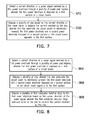
- FIG. 8 is a flowchart of a design method of a power signal transmission structure according to another embodiment of the invention.
- the design method of the power signal transmission structure includes the following steps.
- Step S 810 a current direction of the power signal received by a first power electrode through a plurality of power pad regions is detected.
- the first power electrode is disposed on a first surface of a circuit board.
- Step S 820 a plurality of vias is disposed.
- the vias penetrate the circuit board to electrically connect the first power electrode and a second power electrode disposed on a second surface of the circuit board opposite to the first surface.
- a plurality of first conductor isolation rings is disposed to the first power electrode based on a current direction of the power signal.
- the first conductor isolation rings surround some of the vias to balance the current received by the vias.
- Step S 810 , Step S 820 and Step S 830 The order of Step S 810 , Step S 820 and Step S 830 is described above only for an illustrative purpose, and the embodiments of the invention shall not be limited thereto. Moreover, details of Step S 810 , Step S 820 and Step S 830 may be referred to the embodiments of FIGS. 1 and 3 to 5 and thus will not be repeated hereinafter.
- the vias and/or the conductor isolation rings are disposed according to the current direction of the power signal, so as to balance the current received by the respective vias.
- the respective vias are able to receive the current, and the current sharing by multiple vias is thus facilitated.
Abstract
Description
Claims (3)
Applications Claiming Priority (3)
| Application Number | Priority Date | Filing Date | Title |
|---|---|---|---|
| TW106112493A | 2017-04-14 | ||
| TW106112493A TWI640229B (en) | 2017-04-14 | 2017-04-14 | Power signal transmission structure and design method thereof |
| TW106112493 | 2017-04-14 |
Publications (2)
| Publication Number | Publication Date |
|---|---|
| US20180302978A1 US20180302978A1 (en) | 2018-10-18 |
| US10470299B2 true US10470299B2 (en) | 2019-11-05 |
Family
ID=61972345
Family Applications (1)
| Application Number | Title | Priority Date | Filing Date |
|---|---|---|---|
| US15/934,897 Active US10470299B2 (en) | 2017-04-14 | 2018-03-23 | Power signal transmission structure and design method thereof |
Country Status (3)
| Country | Link |
|---|---|
| US (1) | US10470299B2 (en) |
| EP (1) | EP3389347A1 (en) |
| TW (1) | TWI640229B (en) |
Families Citing this family (1)
| Publication number | Priority date | Publication date | Assignee | Title |
|---|---|---|---|---|
| CN115345124A (en) * | 2022-10-13 | 2022-11-15 | 井芯微电子技术(天津)有限公司 | Current density optimization method and device |
Citations (16)
| Publication number | Priority date | Publication date | Assignee | Title |
|---|---|---|---|---|
| US5618185A (en) * | 1995-03-15 | 1997-04-08 | Hubbell Incorporated | Crosstalk noise reduction connector for telecommunication system |
| US20030047356A1 (en) * | 2001-09-13 | 2003-03-13 | Searls Damion T. | Electronic assembly and a method of constructing an electronic assembly |
| US20040184248A1 (en) * | 2003-03-21 | 2004-09-23 | Intel Corporation | Power delivery apparatus, systems, and methods |
| US20040207989A1 (en) * | 2003-04-18 | 2004-10-21 | International Business Machines Corporation | System and method for improving power distribution current measurement on printed circuit boards |
| US20060050491A1 (en) * | 2004-09-07 | 2006-03-09 | Canon Kabushiki Kaisha | Multilayered printed circuit board |
| US20080054401A1 (en) * | 2006-08-30 | 2008-03-06 | Dongbu Hitek Co., Ltd. | Capacitor structure of semiconductor device |
| US20090251275A1 (en) * | 2008-04-03 | 2009-10-08 | Nec Electronics Corporation | Semiconductor device |
| US20120018199A1 (en) * | 2010-07-23 | 2012-01-26 | Hon Hai Precision Industry Co., Ltd. | Printed circuit board |
| US20120132461A1 (en) * | 2010-11-29 | 2012-05-31 | Hon Hai Precision Industry Co., Ltd. | Printed circuit board |
| US20120243194A1 (en) * | 2011-03-23 | 2012-09-27 | Hon Hai Precision Industry Co., Ltd. | Printed circuit board |
| US20120241207A1 (en) * | 2011-03-24 | 2012-09-27 | Hon Hai Precision Industry Co., Ltd. | Printed circuit board |
| US20140118962A1 (en) * | 2012-10-29 | 2014-05-01 | Cisco Technology, Inc. | Current Redistribution in a Printed Circuit Board |
| US20140334121A1 (en) * | 2012-01-27 | 2014-11-13 | Panasonic Corporation | Multilayer printed circuit board |
| US20150097431A1 (en) * | 2013-10-04 | 2015-04-09 | Fern Nee Tan | Embedded filters for power rail merger |
| JP2015146382A (en) | 2014-02-03 | 2015-08-13 | キヤノン株式会社 | printed circuit board |
| US20170018490A1 (en) * | 2015-07-16 | 2017-01-19 | Delta Electronics (Shanghai) Co., Ltd | Via structure and circuit board having the via structure |
Family Cites Families (1)
| Publication number | Priority date | Publication date | Assignee | Title |
|---|---|---|---|---|
| JP2015149336A (en) * | 2014-02-05 | 2015-08-20 | キヤノン株式会社 | printed circuit board |
-
2017
- 2017-04-14 TW TW106112493A patent/TWI640229B/en active
-
2018
- 2018-03-23 US US15/934,897 patent/US10470299B2/en active Active
- 2018-04-12 EP EP18166917.7A patent/EP3389347A1/en active Pending
Patent Citations (18)
| Publication number | Priority date | Publication date | Assignee | Title |
|---|---|---|---|---|
| US5618185A (en) * | 1995-03-15 | 1997-04-08 | Hubbell Incorporated | Crosstalk noise reduction connector for telecommunication system |
| US20030047356A1 (en) * | 2001-09-13 | 2003-03-13 | Searls Damion T. | Electronic assembly and a method of constructing an electronic assembly |
| US20040184248A1 (en) * | 2003-03-21 | 2004-09-23 | Intel Corporation | Power delivery apparatus, systems, and methods |
| US20040207989A1 (en) * | 2003-04-18 | 2004-10-21 | International Business Machines Corporation | System and method for improving power distribution current measurement on printed circuit boards |
| US20060050491A1 (en) * | 2004-09-07 | 2006-03-09 | Canon Kabushiki Kaisha | Multilayered printed circuit board |
| US20080054401A1 (en) * | 2006-08-30 | 2008-03-06 | Dongbu Hitek Co., Ltd. | Capacitor structure of semiconductor device |
| US20090251275A1 (en) * | 2008-04-03 | 2009-10-08 | Nec Electronics Corporation | Semiconductor device |
| TW201206259A (en) | 2010-07-23 | 2012-02-01 | Hon Hai Prec Ind Co Ltd | Printed circuit board |
| US20120018199A1 (en) * | 2010-07-23 | 2012-01-26 | Hon Hai Precision Industry Co., Ltd. | Printed circuit board |
| US20120132461A1 (en) * | 2010-11-29 | 2012-05-31 | Hon Hai Precision Industry Co., Ltd. | Printed circuit board |
| TW201223359A (en) | 2010-11-29 | 2012-06-01 | Hon Hai Prec Ind Co Ltd | Printed circuit board |
| US20120243194A1 (en) * | 2011-03-23 | 2012-09-27 | Hon Hai Precision Industry Co., Ltd. | Printed circuit board |
| US20120241207A1 (en) * | 2011-03-24 | 2012-09-27 | Hon Hai Precision Industry Co., Ltd. | Printed circuit board |
| US20140334121A1 (en) * | 2012-01-27 | 2014-11-13 | Panasonic Corporation | Multilayer printed circuit board |
| US20140118962A1 (en) * | 2012-10-29 | 2014-05-01 | Cisco Technology, Inc. | Current Redistribution in a Printed Circuit Board |
| US20150097431A1 (en) * | 2013-10-04 | 2015-04-09 | Fern Nee Tan | Embedded filters for power rail merger |
| JP2015146382A (en) | 2014-02-03 | 2015-08-13 | キヤノン株式会社 | printed circuit board |
| US20170018490A1 (en) * | 2015-07-16 | 2017-01-19 | Delta Electronics (Shanghai) Co., Ltd | Via structure and circuit board having the via structure |
Non-Patent Citations (1)
| Title |
|---|
| "Search Report of Europe Counterpart Application", dated Sep. 12, 2018, p. 1-p. 23. |
Also Published As
| Publication number | Publication date |
|---|---|
| TW201838488A (en) | 2018-10-16 |
| EP3389347A1 (en) | 2018-10-17 |
| TWI640229B (en) | 2018-11-01 |
| US20180302978A1 (en) | 2018-10-18 |
Similar Documents
| Publication | Publication Date | Title |
|---|---|---|
| US9544992B2 (en) | PCB having offset differential signal routing | |
| TWI429343B (en) | Printed circuit board | |
| US6646886B1 (en) | Power connection structure | |
| US9775243B2 (en) | Module compliance boards for quad small form-factor pluggable (QSFP) devices | |
| JPWO2017163336A1 (en) | Battery module | |
| CN103219322A (en) | Three dimensional integrated circuit having a resistance measurment structure and method of use | |
| CN109644550A (en) | Flexible circuit board | |
| US11257778B2 (en) | Semi-conductor package structure | |
| US10470299B2 (en) | Power signal transmission structure and design method thereof | |
| US11764151B2 (en) | Connection of several circuits of an electronic chip | |
| US8383955B2 (en) | Printed circuit board | |
| US10490502B2 (en) | Power distribution network of integrated circuit | |
| CN114695331A (en) | Backlight device | |
| JP2004207741A (en) | Signal connection technique between electronic element and signal transmission multilayer pc substrate | |
| US10383298B2 (en) | Apparatus and methods for via connection with reduced via currents | |
| KR20200057524A (en) | A space transformer for a probe card having improved heat dissipation property | |
| KR20160067571A (en) | Printed circuit board | |
| JP2020532864A (en) | Semiconductor devices and contact connection devices between semiconductor devices and circuit boards | |
| KR20200072375A (en) | Printed circuit board | |
| JP2007317888A (en) | Power supply line circuit | |
| TW491004B (en) | Multi-layer substrate of integrated circuit and arrangement method of its via holes | |
| US8878545B2 (en) | Test apparatus with physical separation feature | |
| US20110204507A1 (en) | Two-shelf interconnect | |
| JP2017045813A (en) | Wiring board | |
| US8558390B2 (en) | Semiconductor device |
Legal Events
| Date | Code | Title | Description |
|---|---|---|---|
| AS | Assignment |
Owner name: PEGATRON CORPORATION, TAIWAN Free format text: ASSIGNMENT OF ASSIGNORS INTEREST;ASSIGNORS:YANG, CHING OU;CHU, CHENG-HUI;REEL/FRAME:045336/0392 Effective date: 20180110 |
|
| FEPP | Fee payment procedure |
Free format text: ENTITY STATUS SET TO UNDISCOUNTED (ORIGINAL EVENT CODE: BIG.); ENTITY STATUS OF PATENT OWNER: LARGE ENTITY |
|
| STPP | Information on status: patent application and granting procedure in general |
Free format text: FINAL REJECTION MAILED |
|
| STPP | Information on status: patent application and granting procedure in general |
Free format text: ADVISORY ACTION MAILED |
|
| STPP | Information on status: patent application and granting procedure in general |
Free format text: DOCKETED NEW CASE - READY FOR EXAMINATION |
|
| STPP | Information on status: patent application and granting procedure in general |
Free format text: NOTICE OF ALLOWANCE MAILED -- APPLICATION RECEIVED IN OFFICE OF PUBLICATIONS |
|
| STPP | Information on status: patent application and granting procedure in general |
Free format text: PUBLICATIONS -- ISSUE FEE PAYMENT VERIFIED |
|
| STCF | Information on status: patent grant |
Free format text: PATENTED CASE |
|
| MAFP | Maintenance fee payment |
Free format text: PAYMENT OF MAINTENANCE FEE, 4TH YEAR, LARGE ENTITY (ORIGINAL EVENT CODE: M1551); ENTITY STATUS OF PATENT OWNER: LARGE ENTITY Year of fee payment: 4 |