US10451666B2 - Methodology for early detection of TS to PC short issue - Google Patents
Methodology for early detection of TS to PC short issue Download PDFInfo
- Publication number
- US10451666B2 US10451666B2 US14/989,109 US201614989109A US10451666B2 US 10451666 B2 US10451666 B2 US 10451666B2 US 201614989109 A US201614989109 A US 201614989109A US 10451666 B2 US10451666 B2 US 10451666B2
- Authority
- US
- United States
- Prior art keywords
- node
- gnd
- structures
- determining
- bvc
- Prior art date
- Legal status (The legal status is an assumption and is not a legal conclusion. Google has not performed a legal analysis and makes no representation as to the accuracy of the status listed.)
- Expired - Fee Related, expires
Links
- 238000000034 method Methods 0.000 title claims abstract description 57
- 238000001514 detection method Methods 0.000 title abstract description 18
- 238000007689 inspection Methods 0.000 claims abstract description 36
- 238000012360 testing method Methods 0.000 claims description 31
- 230000008569 process Effects 0.000 claims description 30
- 238000012544 monitoring process Methods 0.000 claims description 18
- 238000005259 measurement Methods 0.000 claims description 12
- 238000012986 modification Methods 0.000 claims description 7
- 230000004048 modification Effects 0.000 claims description 7
- 238000010894 electron beam technology Methods 0.000 claims description 3
- 230000007547 defect Effects 0.000 abstract description 36
- 239000000758 substrate Substances 0.000 abstract description 20
- 238000012545 processing Methods 0.000 abstract description 10
- 239000004065 semiconductor Substances 0.000 abstract description 5
- 238000004088 simulation Methods 0.000 description 10
- 238000013461 design Methods 0.000 description 9
- 238000004519 manufacturing process Methods 0.000 description 7
- 238000005516 engineering process Methods 0.000 description 5
- 230000009977 dual effect Effects 0.000 description 4
- 230000000694 effects Effects 0.000 description 4
- 238000001914 filtration Methods 0.000 description 4
- 230000003287 optical effect Effects 0.000 description 3
- 230000001629 suppression Effects 0.000 description 3
- 230000003247 decreasing effect Effects 0.000 description 2
- 238000005286 illumination Methods 0.000 description 2
- 239000010410 layer Substances 0.000 description 2
- 230000007246 mechanism Effects 0.000 description 2
- 230000005855 radiation Effects 0.000 description 2
- RTAQQCXQSZGOHL-UHFFFAOYSA-N Titanium Chemical group [Ti] RTAQQCXQSZGOHL-UHFFFAOYSA-N 0.000 description 1
- 230000004888 barrier function Effects 0.000 description 1
- 230000015572 biosynthetic process Effects 0.000 description 1
- 230000001413 cellular effect Effects 0.000 description 1
- 238000012512 characterization method Methods 0.000 description 1
- 239000013078 crystal Substances 0.000 description 1
- 230000001627 detrimental effect Effects 0.000 description 1
- 238000011161 development Methods 0.000 description 1
- 238000010586 diagram Methods 0.000 description 1
- 230000005669 field effect Effects 0.000 description 1
- 239000004615 ingredient Substances 0.000 description 1
- 239000011229 interlayer Substances 0.000 description 1
- 238000013507 mapping Methods 0.000 description 1
- 239000000463 material Substances 0.000 description 1
- 230000006855 networking Effects 0.000 description 1
- 230000002093 peripheral effect Effects 0.000 description 1
- 238000005498 polishing Methods 0.000 description 1
- 230000003068 static effect Effects 0.000 description 1
- 239000000126 substance Substances 0.000 description 1
- 239000011800 void material Substances 0.000 description 1
- 235000012431 wafers Nutrition 0.000 description 1
Images


Classifications
-
- G—PHYSICS
- G01—MEASURING; TESTING
- G01R—MEASURING ELECTRIC VARIABLES; MEASURING MAGNETIC VARIABLES
- G01R31/00—Arrangements for testing electric properties; Arrangements for locating electric faults; Arrangements for electrical testing characterised by what is being tested not provided for elsewhere
- G01R31/28—Testing of electronic circuits, e.g. by signal tracer
- G01R31/2801—Testing of printed circuits, backplanes, motherboards, hybrid circuits or carriers for multichip packages [MCP]
- G01R31/281—Specific types of tests or tests for a specific type of fault, e.g. thermal mapping, shorts testing
- G01R31/2812—Checking for open circuits or shorts, e.g. solder bridges; Testing conductivity, resistivity or impedance
-
- H—ELECTRICITY
- H01—ELECTRIC ELEMENTS
- H01L—SEMICONDUCTOR DEVICES NOT COVERED BY CLASS H10
- H01L22/00—Testing or measuring during manufacture or treatment; Reliability measurements, i.e. testing of parts without further processing to modify the parts as such; Structural arrangements therefor
- H01L22/10—Measuring as part of the manufacturing process
- H01L22/14—Measuring as part of the manufacturing process for electrical parameters, e.g. resistance, deep-levels, CV, diffusions by electrical means
-
- H—ELECTRICITY
- H01—ELECTRIC ELEMENTS
- H01L—SEMICONDUCTOR DEVICES NOT COVERED BY CLASS H10
- H01L22/00—Testing or measuring during manufacture or treatment; Reliability measurements, i.e. testing of parts without further processing to modify the parts as such; Structural arrangements therefor
- H01L22/20—Sequence of activities consisting of a plurality of measurements, corrections, marking or sorting steps
-
- H01L27/1104—
-
- H—ELECTRICITY
- H01—ELECTRIC ELEMENTS
- H01L—SEMICONDUCTOR DEVICES NOT COVERED BY CLASS H10
- H01L29/00—Semiconductor devices adapted for rectifying, amplifying, oscillating or switching, or capacitors or resistors with at least one potential-jump barrier or surface barrier, e.g. PN junction depletion layer or carrier concentration layer; Details of semiconductor bodies or of electrodes thereof ; Multistep manufacturing processes therefor
- H01L29/66—Types of semiconductor device ; Multistep manufacturing processes therefor
- H01L29/66007—Multistep manufacturing processes
- H01L29/66075—Multistep manufacturing processes of devices having semiconductor bodies comprising group 14 or group 13/15 materials
- H01L29/66227—Multistep manufacturing processes of devices having semiconductor bodies comprising group 14 or group 13/15 materials the devices being controllable only by the electric current supplied or the electric potential applied, to an electrode which does not carry the current to be rectified, amplified or switched, e.g. three-terminal devices
- H01L29/66409—Unipolar field-effect transistors
- H01L29/66477—Unipolar field-effect transistors with an insulated gate, i.e. MISFET
-
- H—ELECTRICITY
- H10—SEMICONDUCTOR DEVICES; ELECTRIC SOLID-STATE DEVICES NOT OTHERWISE PROVIDED FOR
- H10B—ELECTRONIC MEMORY DEVICES
- H10B10/00—Static random access memory [SRAM] devices
- H10B10/12—Static random access memory [SRAM] devices comprising a MOSFET load element
-
- G—PHYSICS
- G01—MEASURING; TESTING
- G01R—MEASURING ELECTRIC VARIABLES; MEASURING MAGNETIC VARIABLES
- G01R31/00—Arrangements for testing electric properties; Arrangements for locating electric faults; Arrangements for electrical testing characterised by what is being tested not provided for elsewhere
- G01R31/26—Testing of individual semiconductor devices
- G01R31/27—Testing of devices without physical removal from the circuit of which they form part, e.g. compensating for effects surrounding elements
- G01R31/275—Testing of devices without physical removal from the circuit of which they form part, e.g. compensating for effects surrounding elements for testing individual semiconductor components within integrated circuits
-
- G—PHYSICS
- G01—MEASURING; TESTING
- G01R—MEASURING ELECTRIC VARIABLES; MEASURING MAGNETIC VARIABLES
- G01R31/00—Arrangements for testing electric properties; Arrangements for locating electric faults; Arrangements for electrical testing characterised by what is being tested not provided for elsewhere
- G01R31/28—Testing of electronic circuits, e.g. by signal tracer
- G01R31/302—Contactless testing
- G01R31/305—Contactless testing using electron beams
- G01R31/307—Contactless testing using electron beams of integrated circuits
-
- H—ELECTRICITY
- H01—ELECTRIC ELEMENTS
- H01L—SEMICONDUCTOR DEVICES NOT COVERED BY CLASS H10
- H01L22/00—Testing or measuring during manufacture or treatment; Reliability measurements, i.e. testing of parts without further processing to modify the parts as such; Structural arrangements therefor
- H01L22/10—Measuring as part of the manufacturing process
- H01L22/12—Measuring as part of the manufacturing process for structural parameters, e.g. thickness, line width, refractive index, temperature, warp, bond strength, defects, optical inspection, electrical measurement of structural dimensions, metallurgic measurement of diffusions
Definitions
- the present disclosure relates to a manufacture of metal-oxide-semiconductor field-effect transistor (MOSFET) devices.
- MOSFET metal-oxide-semiconductor field-effect transistor
- the present disclosure is particularly applicable to detecting source/drain (TS) to gate (PC) (TS-PC) shorts for the 14 nanometer (nm) technology node and beyond.
- TS source/drain
- PC gate
- TS-PC short defects are some of the most common and detrimental failure mechanisms for advanced process technology development in MOSFET device manufacturing. In-line detection of TS-PC short defects is especially challenging for new shorting mechanisms that can occur on an atomic scale due to new material/process flow implementation. Generally, critical TS-PC short defects cannot be detected by optical inspection methodology due to both resolution and contrast limitations.
- Electron beam inspection has been the most popular in-line detection method for detecting TS-PC electric defects at the gate contact (CB) chemical mechanical polishing (CMP) (CB-CMP) stage of device processing.
- CB-CMP is the only check point for TS-PC short defects.
- the cycle time is too long and, therefore, a defect may already be present at the TS-CMP stage.
- Detection of TS-PC short defects at the TS-CMP stage is currently not possible due to fundamental challenges.
- Early detection of TS-PC short defects at the TS-CMP stage is of great practical value in terms of cycle time, early warning of process excursion, and reducing costs for high volume manufacturing.
- An aspect of the present disclosure is a method of dual condition physics filtering and/or bright voltage contrast (BVC) nuisance suppression to enable in-line detection of TS-PC short defects at the TS-CMP processing stage.
- BVC bright voltage contrast
- Another aspect of the present disclosure is a method of detecting TS-PC short defects through channel assisted conduction (CAC) based on a share contact (SC) design at the TS-CMP layer.
- CAC channel assisted conduction
- SC share contact
- a further aspect of the present disclosure is a method of monitoring and measuring TS-PC overlay (OVL) shift and process window variation based on in-line EBI scan results.
- OTL TS-PC overlay
- some technical effects may be achieved in part by a method including: providing a semiconductor substrate, the substrate having a plurality of partially formed MOSFET devices; performing a first defect inspection on the substrate, the first inspection including advanced charging control (ACC); identifying one or more BVC candidates on the substrate based on the first inspection; performing a second defect inspection on the one or more BVC candidates, the second inspection performed without ACC; and detecting one or more BVC defects on the substrate based on the one or more BVC candidates appearing during both the first and second inspections.
- Aspects of the present disclosure include the first and second defect inspections being EBI. Other aspects include each of the one or more BVC defects being a source/drain to gate short.
- Another aspect of the present disclosure is a method including: forming a static random-access memory (SRAM) device with at least one n-node, at least one p-node, and at least one share contact, the at least one share contact connecting the at least one n-node to the at least one p-node; determining an upper limit of a threshold voltage (Vt) for the n-node; applying a voltage less than or equal to the upper limit to at least one source/drain (S/D) of the n-node; and determining whether a TS-PC short is present on the n-node based on the application of the voltage.
- SRAM static random-access memory
- aspects of the present disclosure include the at least one p-node functioning as a virtual ground for the n-node.
- Other aspects include the Vt being less than one-half of the at least one S/D voltage (Vd).
- Further aspects include determining whether the TS-PC short is present based on CAC caused by an EBI.
- a further aspect of the present disclosure is a method including: providing a test device for OVL shift monitoring and measurement, the test device having an n-node, a p-node, and a plurality of ground (GND), bit line (BL), SC, voltage supply (Vdd), active channel region (Rx), and gate structures; modifying a width, a height, and/or a position of one or more BL and/or GND structures on one or more rows of the n-node; performing an EBI on the one or more rows of the n-node; determining an order of OVL shift between a TS and PC of the n-node based on BVC results from the EBI; and determining a measure of the OVL shift in an X-direction or a Y-direction based on the BVC results.
- GDD ground
- BL bit line
- Vdd voltage supply
- Rx active channel region
- aspects of the present disclosure include determining the order of the OVL shift in an X-direction by: modifying a width of sequential BL and GND structures on the one or more rows of the n-node.
- Other aspects include determining at least one process window variation and/or at least one TS misalignment based on the BVC results.
- Further aspects include, wherein the measure of the OVL shift is based on the at least one process window variation, modifying the width of the BL or GND structures by: adjusting a first BL or GND structure so that the first BL or GND structure just starts touching adjacent gate contacts; and modifying the width of the sequential BL or GND structures until a last BL or GND structure on the one or more rows can no longer be subsequently printed.
- Additional aspects include, wherein the measure of the OVL shift is based on the at least one TS misalignment, modifying the width by: starting with a first width of a first BL or GND structure; and modifying the width of the sequential BL or GND structures until a last BL or GND structure on the one or more rows can no longer be subsequently printed.
- Another aspect includes determining the measure of OVL shift in a +X or ⁇ X direction by: disconnecting a first group of SC structures for a first row and a second group of SC structures for a second row of the one or more rows on the n-node before modifying the width of sequential BL and GND structures on the first and second rows.
- aspects include determining the measure of the OVL shift in an X-direction by: modifying a position of sequential BL and GND structures on the one or more rows of the n-node relative to one or more adjacent gate structures, respectively, on the one or more rows; and determining the measure of the OVL shift in a Y-direction by: modifying a position of one or more GND structures on the one or more rows of the n-node relative to one or more Vdd structures, respectively, on one or more adjacent rows on the n-node. Further aspects include determining the measure of the OVL shift in an X or a Y direction by: monitoring an order of the BVC results based on the modification.
- Additional aspects include determining the measure of the OVL shift in an +X or ⁇ X or a +Y or ⁇ Y direction, respectively, by: determining which row of the one or more rows corresponding to the BVC results are dominant.
- Another aspect includes determining the order of the OVL shift in a Y-direction by: modifying a height of sequential GND structures on the one or more rows of the n-node.
- Other aspects include the maximum height of the sequential GND structures being limited by a GND to Vdd space along the Y-direction.
- Further aspects include determining the measure of the OVL shift in the Y-direction by: monitoring an order of the BVC results based on the modification.
- Additional aspects include determining the measure of the OVL shift in a +Y or ⁇ Y direction by: determining which row of the one or more rows corresponding to the BVC results are dominant.
- FIG. 1 illustrates a process flow for dual condition physics filtering and/or BVC nuisance suppression to enable in-line detection of TS-PC short defects at the TS-CMP processing stage, in accordance with an exemplary embodiment
- FIGS. 2A and 2B schematically illustrate a SC design that enables in-line detection of TS-PC short defects by CAC and the physical principle of CAC under ebeam exposure, respectively, in accordance with an exemplary embodiment
- FIGS. 3A and 3B schematically illustrate a test structure for monitoring and measurement of OVL shift in an X-direction based on contact size modulation, in accordance with an exemplary embodiment
- FIGS. 4A and 4B schematically illustrate a simulation case of the TS misalignment measure from the test structure of FIGS. 3A and 3B , in accordance with an exemplary embodiment
- FIG. 5 schematically illustrates a test structure for vector-based in-line monitoring and measurement of OVL shift in an X-direction based on contact size modulation, in accordance with another exemplary embodiment
- FIGS. 6A and 6B schematically illustrate a simulation case of the TS misalignment measure from the test structure of FIG. 5 , in accordance with an exemplary embodiment
- FIG. 7 schematically illustrates a test structure for in-line monitoring and measurement of OVL shift in an X-direction based on contact position modulation, in accordance with an exemplary embodiment
- FIG. 8 schematically illustrates a simulation case of the TS misalignment measure from the test structure of FIG. 7 , in accordance with an exemplary embodiment
- FIG. 9 schematically illustrates a test structure for in-line monitoring and measurement of OVL shift in a Y-direction based on contact size modulation, in accordance with an exemplary embodiment
- FIG. 10 schematically illustrates a simulation case of TS misalignment measure from the test structure of FIG. 9 , in accordance with an exemplary embodiment
- FIG. 11 schematically illustrates a test structure for in-line monitoring and measurement of OVL shift in a Y-direction based on contact position modulation, in accordance with an exemplary embodiment
- FIG. 12 schematically illustrates a simulation case of TS misalignment measure from the test structure of FIG. 11 , in accordance with an exemplary embodiment.
- the present disclosure addresses and solves the current problem of an inability to detect TS-PC short defects in-line at the TS-CMP processing stage attendant upon EBI inspection during MOSFET device formation.
- Methodology in accordance with embodiments of the present disclosure includes providing a semiconductor substrate, the substrate having a plurality of partially formed MOSFET devices.
- a defect inspection is performed on the substrate, in which the inspection includes ACC.
- One or more BVC candidates on the substrate are identified based on the inspection, and a second defect inspection is performed on the one or more BVC candidates, the second inspection being performed without ACC.
- One or more BVC defects are then detected on the substrate based on the one or more BVC candidates appearing during both inspections.
- FIG. 1 illustrates a process flow for dual condition physics filtering and/or BVC nuisance suppression to enable in-line detection of TS-PC short defects at the TS-CMP processing stage.
- a semiconductor substrate with a plurality of partially formed MOSFET devices is provided for defect inspection, e.g., by EBI.
- EBI defect inspection
- there is no detectable voltage contrast (VC) signal at the TS-CMP level because both the gates and n-nodes of a device are “floating” and, therefore, will appear dark as a result of EBI.
- the p-nodes of the device are grounded and, therefore, will appear bright as a result of EBI.
- a defect inspection is then performed on the substrate with ACC turned on, e.g., laser radiation from scanning the substrate with an electron beam (ebeam).
- ACC e.g., laser radiation from scanning the substrate with an electron beam (ebeam).
- ebeam electron beam
- ACC is turned on, a more uniform and stable charging state can be obtained, but false BVC results can also occur as a result of junction leakage induced by the optical radiation. Consequently, the results of a defect inspection performed only with ACC on will be overwhelmed by nuisance/noise rate and, therefore, prevent accurate BVC detection.
- step 103 the BVC candidates resulting from the first inspection are classified by on-tool automatic defect classification (ADC), and then the various BVC candidates are inspected again without ACC.
- ADC on-tool automatic defect classification
- the second inspection without ACC many of the BVC candidates from the first inspection will no longer be visible because of the enhanced n-p junction barrier height without laser illumination.
- simply performing the inspection without ACC is also insufficient because of the resulting nuisance/noise due to non-uniform charging and/or image artifacts.
- step 105 the BVC candidates are examined to determine whether the BVC is still visible after the second inspection. If a BVC candidate from the first inspection is no longer visible after the second inspection, then in step 107 , those BVC candidates are determined not to be BVC defects, but rather nuisance due to optically induced leakage. In contrast, if a BVC candidate from the first inspection is still visible after the second inspection, then in step 109 , those BVC candidates are determined to be real BVC due to an electrical short, e.g., a TS-PC short. Thus, the second inspection without optical illumination can serve as a physics filter to separate nuisance due to optically induced junction leakage. In step 111 , once the one or more BVC candidates are identified as true or real BVC defects on the substrate, the final data is outputted for further device processing.
- FIGS. 2A and 2B (an orthographic view and a cross-sectional view) schematically illustrate a SC design that enables in-line detection of TS-PC short defects by CAC and the physical principle of CAC under ebeam exposure, respectively, in accordance with an exemplary embodiment. Adverting to FIG.
- a 14 nm SRAM device 201 e.g., a pull-down terminal, is formed with an n-node 203 , a p-node 205 , and a SC 207 , which connects the n-node 203 and the p-node 205 via the S/D contact 209 of the p-node 205 and the S/D contact 211 of the n-node 203 .
- the p-node 205 has a relatively low resistance and, therefore, provides a virtual ground for the neighboring n-node 203 .
- the n-node 203 also includes a gate contact 213 , a S/D contact 215 , and a channel 217 . Further, a TS-PC short, e.g., a STI void, titanium residue, fin crystal defect, or OVL shift, has occurred in the n-node 203 during manufacturing as represented by the bar 219 .
- the design of the SRAM device 201 is limited to the 14 nm technology node and beyond because larger technology nodes, e.g., the 20 nm, do not include share contacts and, therefore, TS-PC short detection at the TS-CMP processing stage is not possible since both the n-node junction and gate contacts are “floating.”
- Vt threshold voltage
- V t V t
- V t V d 2 .
- the surface potential can be varied by changing the injected ebeam current.
- the surface potential of the p-node 205 (forward biased P-N junction) under a positive charge condition is basically “pinned” (e.g., around 0.7-0.8 V) and, therefore, results in an almost flat grey level value (GLV) despite increasing the applied ebeam current.
- the reversed biased n-node 203 potential can continue to increase with increased current and the resulting GLV will correspondingly decrease. Without the SC 207 , the S/D contacts 211 and 215 would remain floating and, therefore, appear dark despite the presence of the TS-PC short 219 .
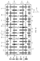
- FIGS. 3A and 3B schematically illustrate a test structure for in-line monitoring and measurement of OVL shift in an X-direction based on contact size modulation, according to an exemplary embodiment.
- a test device 301 Adverting to FIG. 3A , a test device 301 is formed with n-nodes 303 and 305 and a plurality of p-nodes 307 .
- the test device 301 also includes a plurality of GND 309 , BL 311 , SC 313 , Vdd 315 , Rx 317 , and gate 319 structures. From a junction design point of view, there is no difference between the BL 311 and GND 309 contacts.
- a precise metric for TS-PC alignment can be set. For example the width of GND 309 (W 0 and W 2 ) and BL 311 (W 1 and W 3 ) may be increased and the width of GND 309 (W 4 and W 6 ) and BL 311 (W 5 ) may be decreased.
- the starting point of the n-node contact width can be set to where a TS contact, e.g., GND 309 , just starts to touch adjacent gate contacts 319 (depending on design rule and process), as depicted in FIG. 3B (a cross-sectional view).
- a TS contact e.g., GND 309
- FIG. 3B a cross-sectional view
- an interlayer dielectric (ILD) 321 is formed between the gate contacts 319 , and the SC 313 , gate contacts 319 , GND 309 , and BL 311 are all formed on a substrate 323 .
- the process window of a conventional process can be obtained from the order (f) of observed BVC, i.e., starting from W 0 up to i th BVC can be visible from the stand-alone gradually modulated n-node 303 and 305 contacts.
- the maximum order of modulated TS contact width can be determined from the maximum printability of the corresponding process.
- the accuracy of the TS misalignment can be determined by the half of the step: ⁇ W/2.
- the starting point of W 0 can be arbitrary since only relative TS misalignment, i.e., relative measure, is needed compared to the conventional process.
- FIGS. 4A and 4B schematically illustrate a simulation case based on the test structure of FIGS. 3A and 3B , in accordance with an exemplary embodiment.
- FIG. 4A represents a conventional process window
- FIG. 4B represents a TS misalignment.
- the width of the TS contacts of the n-node 305 e.g., GND 309 or BL 311
- the width of the TS contacts of the n-node 305 have already been modulated as described above, e.g., by increasing the width of TS contacts W 0 -W 3 and by decreasing the width of TS contacts W 4 -W 7 .
- PW i ⁇ ⁇ ⁇ ⁇ W 2 in the case where W0 starts from the point of just touching adjacent gates 319 (not shown for illustrative convenience).
- the TS contacts W 0 -W 6 of FIG. 4B appear bright and, therefore, correspond to a TS-PC short, whereas the TS contact W 7 appears dark and, therefore, has no short.
- up to i 2 th order of BVC is visible from the modulated n-node 305 of the test structure 301 .
- the TS misalignment may be determined, for example, from the equation:
- TS misalignment ( i 2 - i 1 ) ⁇ ⁇ ⁇ ⁇ W 2 .
- FIG. 5 schematically illustrates a test structure for vector-based in-line monitoring and measurement of OVL shift in an X-direction based on contact size modulation, in accordance with another exemplary embodiment.
- the test device and process flow of FIG. 5 is identical to that of FIG.
- Disconnecting the SC 313 on the left side of the TS contacts on the n-node 303 and the SC 313 on the right side of the TS contacts on the n-node 305 enables a measuring of not only the amount of OVL shift, but also along which direction (+X or ⁇ X) the TS misalignment is occurring.
- the test device of FIG. 5 yields a vector-based mapping of the OVL shift in an X-direction.
- FIGS. 6A and 6B schematically illustrate a simulation case based on the test structure of FIG. 5 , in accordance with an exemplary embodiment.
- the TS contacts e.g., the BL 311 W 1 on the n-node 305 and the GND 309 W 2 on n-node 303
- the TS contacts can only be bright due to a short/shift to the nearby SC 313 , e.g., in the +X direction, as depicted by the arrow 601 .
- a shift direction can be identified by comparing the particular BVC pattern from two sets of alternatively arranged test structures, e.g., n-nodes 303 and 305 . Adverting to FIG. 6B , if the OVL shift is along the opposite X-direction, e.g., ⁇ X, then the polarity of the pattern will be reversed, as depicted by the arrow 603 .
- the TS contacts on the n-node 303 are shifted in one direction, e.g., ⁇ X, and the TS contacts on the n-node 305 are shifted in the opposite direction, e.g., +X.
- the specific direction of the movement of the TS contacts on a particular n-node is not significant as long as one set moves in one direction and the other set moves in the opposite direction.
- the maximum number of steps is determined by the TS-PC spacing: ATP, i.e., the maximum modulation depth:
- the OVL shift can be determined from the order of the TS BVC due to a TS-PC short, and the OVL shift in an X-direction can be determined from which n-node pattern, e.g., n-node 303 or n-node 305 , shows dominant BVC.
- FIG. 8 schematically illustrates a simulation case of the TS misalignment measure from the test structure of FIG. 7 , in accordance with an exemplary embodiment.
- the OVL shift along the X-direction can be monitored and measured by determining, for example, which n-node pattern row shows dominant BVC.
- the row corresponding to the n-node 303 shows a dominant BVC pattern, e.g., BL 311 W 3 , W 5 , and W 7 and GND 309 W 4 and W 6 all appear bright.
- BL 311 W 7 of the n-node 305 appears bright. Therefore, the dominant pattern indicates an OVL shift along the +X direction, as depicted by the arrow 801 .
- Relative TS misalignment compared to the conventional process is still valid by comparing BVC order from two wafers.
- FIG. 9 schematically illustrates a test structure for in-line monitoring and measurement of OVL shift in a Y-direction based on contact size modulation, in accordance with an exemplary embodiment.
- the modulation of the one or more TS contacts for Y-shift is only applicable to the GND 309 structures due to their proximity to Vdd 315 on the p-nodes 307 , as depicted in FIG. 9 .
- the OVL shift along a Y-direction can be determined.
- two sets of modulated GND 309 contact patterns can be used to determine the actual Y-direction shift, e.g., +Y or ⁇ Y.
- FIG. 10 schematically illustrates a simulation case of TS misalignment measure from the test structure of FIG. 9 , in accordance with an exemplary embodiment.
- the OVL shift along a Y-direction can be monitored and measured by determining, for example, which n-node pattern row shows dominant BVC.
- the GND 309 W 0 , W 2 , and W 4 of n-node 303 all appear bright, whereas only the GND 309 W 0 of n-node 305 appears bright. Therefore, the dominant n-node pattern indicates an OVL shift along the +Y direction, as depicted by the arrow 1001 .
- FIG. 11 schematically illustrates a test structure for in-line monitoring and measurement of OVL shift in a Y-direction based on contact position modulation, in accordance with an exemplary embodiment.
- the Y shift is symmetric in both +Y and ⁇ Y directions, e.g., one GND pattern shifts in the +Y direction, e.g., the GND 309 of n-node 303 , and one GND pattern shifts in the ⁇ Y direction, e.g., the GND 309 of n-node 305 .
- the shift direction can be determined from which set of n-node patterns is turned bright from the EBI scan and the shift amount can be determined from the order of the BVC pattern.
- FIG. 12 schematically illustrates a simulation case of TS misalignment measure from the test structure of FIG. 11 , in accordance with an exemplary embodiment.
- the OVL shift along a Y-direction can be monitored and measured by determining, for example, which n-node pattern row shows dominant BVC.
- the GND 309 W 2 , W 4 , and W 6 of n-node 303 all appear bright, whereas only the GND 309 W 6 of n-node 305 appears bright. Therefore, the dominant n-node pattern indicates an OVL shift along the +Y direction, as depicted by the arrow 1201 .
- the embodiments of the present disclosure can achieve several technical effects including dual condition physics filtering to effectively separate nuisance and enable detection of ground true electric short defects; enabling in-line detection of TS-PC short through CAC based on a SC design at the TS-CMP layer; eliminating resolution limitations; being fully compatible with a conventional process and, therefore, can represent the real process issue of chip production; and providing real time and reliable characterization beyond OVL control limit.
- Embodiments of the present disclosure enjoy utility in various industrial applications as, for example, microprocessors, smart phones, mobile phones, cellular handsets, set-top boxes, DVD recorders and players, automotive navigation, printers and peripherals, networking and telecom equipment, gaming systems, and digital cameras. The present disclosure therefore enjoys industrial applicability in any of the 14 nm technology node and beyond.
Abstract
Description
In particular, to switch on the
Thus, detection of a TS-PC short on the floating n-
in the case where W0 starts from the point of just touching adjacent gates 319 (not shown for illustrative convenience).
For determining TS misalignment only relative measure is needed. Consequently, the TS misalignment (W4-W6) may be determined from comparison with the conventional process.
The OVL shift can be determined from the order of the TS BVC due to a TS-PC short, and the OVL shift in an X-direction can be determined from which n-node pattern, e.g., n-
Similar to modifying the TS contact size in
The Y shift is symmetric in both +Y and −Y directions, e.g., one GND pattern shifts in the +Y direction, e.g., the
Claims (13)
Priority Applications (3)
| Application Number | Priority Date | Filing Date | Title |
|---|---|---|---|
| US14/989,109 US10451666B2 (en) | 2016-01-06 | 2016-01-06 | Methodology for early detection of TS to PC short issue |
| TW105138842A TWI624674B (en) | 2016-01-06 | 2016-11-25 | Methodology for early detection of ts to pc short issue |
| CN201710006926.5A CN107026099B (en) | 2016-01-06 | 2017-01-05 | Method for early detection of TS-to-PC short circuit problem |
Applications Claiming Priority (1)
| Application Number | Priority Date | Filing Date | Title |
|---|---|---|---|
| US14/989,109 US10451666B2 (en) | 2016-01-06 | 2016-01-06 | Methodology for early detection of TS to PC short issue |
Publications (2)
| Publication Number | Publication Date |
|---|---|
| US20170192050A1 US20170192050A1 (en) | 2017-07-06 |
| US10451666B2 true US10451666B2 (en) | 2019-10-22 |
Family
ID=59226277
Family Applications (1)
| Application Number | Title | Priority Date | Filing Date |
|---|---|---|---|
| US14/989,109 Expired - Fee Related US10451666B2 (en) | 2016-01-06 | 2016-01-06 | Methodology for early detection of TS to PC short issue |
Country Status (3)
| Country | Link |
|---|---|
| US (1) | US10451666B2 (en) |
| CN (1) | CN107026099B (en) |
| TW (1) | TWI624674B (en) |
Families Citing this family (10)
| Publication number | Priority date | Publication date | Assignee | Title |
|---|---|---|---|---|
| DE102017127641A1 (en) * | 2016-12-15 | 2018-06-21 | Taiwan Semiconductor Manufacturing Co., Ltd. | Method for bridging testing in adjacent semiconductor devices and test setup |
| JP6942555B2 (en) * | 2017-08-03 | 2021-09-29 | 東京エレクトロン株式会社 | Board processing method, computer storage medium and board processing system |
| KR102600786B1 (en) | 2018-04-20 | 2023-11-10 | 삼성전자주식회사 | Semiconductor device including test structure |
| CN110690195B (en) * | 2018-07-05 | 2021-05-04 | 中芯国际集成电路制造(上海)有限公司 | Test structure of semiconductor device and test method thereof |
| KR102626334B1 (en) | 2018-07-27 | 2024-01-16 | 삼성전자주식회사 | Semiconductor device and method for fabricating the same |
| KR102645944B1 (en) | 2018-10-10 | 2024-03-08 | 삼성전자주식회사 | Semiconductor device and method for fabricating the same |
| CN109872766B (en) * | 2019-02-15 | 2021-07-16 | 长江存储科技有限责任公司 | Failure analysis method of three-dimensional memory |
| CN110876279B (en) * | 2019-10-12 | 2021-03-12 | 长江存储科技有限责任公司 | Method for detecting defects in depth features using laser enhanced electron tunneling effect |
| KR20210097259A (en) | 2020-01-29 | 2021-08-09 | 삼성전자주식회사 | Testing method of semiconductor device |
| CN113345865B (en) * | 2021-05-28 | 2022-09-09 | 福建省晋华集成电路有限公司 | Semiconductor test structure and defect detection method |
Citations (9)
| Publication number | Priority date | Publication date | Assignee | Title |
|---|---|---|---|---|
| US20070222470A1 (en) * | 2006-03-22 | 2007-09-27 | International Business Machines Corporation | Buried short location determination using voltage contrast inspection |
| US20090196490A1 (en) * | 2008-02-06 | 2009-08-06 | Fujitsu Microelectronics Limited | Defect inspection method and defect inspection apparatus |
| CN101630623A (en) | 2003-05-09 | 2010-01-20 | 株式会社荏原制作所 | Inspection apparatus by charged particle beam and method for manufacturing device using inspection apparatus |
| TW201037778A (en) | 2009-04-08 | 2010-10-16 | Hermes Microvision Inc | Test structure for charged particle beam inspection and method for defect determination using the same |
| US20100278416A1 (en) * | 2009-04-30 | 2010-11-04 | Hong Xiao | Method for Inspecting Overlay Shift Defect during Semiconductor Manufacturing and Apparatus Thereof |
| CN103543365A (en) | 2012-07-10 | 2014-01-29 | 中芯国际集成电路制造(上海)有限公司 | Test structure and test method for minimum distances of interconnection structures |
| US8736084B2 (en) * | 2011-12-08 | 2014-05-27 | Taiwan Semiconductor Manufacturing Company, Ltd. | Structure and method for E-beam in-chip overlay mark |
| CN103943609A (en) | 2014-03-24 | 2014-07-23 | 上海华力微电子有限公司 | Structure for testing integrity of grid boundary oxide layer |
| TWI512304B (en) | 2005-09-13 | 2015-12-11 | Ebara Corp | Semiconductor device and method for inspecting the semiconductor |
-
2016
- 2016-01-06 US US14/989,109 patent/US10451666B2/en not_active Expired - Fee Related
- 2016-11-25 TW TW105138842A patent/TWI624674B/en not_active IP Right Cessation
-
2017
- 2017-01-05 CN CN201710006926.5A patent/CN107026099B/en not_active Expired - Fee Related
Patent Citations (10)
| Publication number | Priority date | Publication date | Assignee | Title |
|---|---|---|---|---|
| CN101630623A (en) | 2003-05-09 | 2010-01-20 | 株式会社荏原制作所 | Inspection apparatus by charged particle beam and method for manufacturing device using inspection apparatus |
| TWI512304B (en) | 2005-09-13 | 2015-12-11 | Ebara Corp | Semiconductor device and method for inspecting the semiconductor |
| US20070222470A1 (en) * | 2006-03-22 | 2007-09-27 | International Business Machines Corporation | Buried short location determination using voltage contrast inspection |
| US20090196490A1 (en) * | 2008-02-06 | 2009-08-06 | Fujitsu Microelectronics Limited | Defect inspection method and defect inspection apparatus |
| TW201037778A (en) | 2009-04-08 | 2010-10-16 | Hermes Microvision Inc | Test structure for charged particle beam inspection and method for defect determination using the same |
| TWI409893B (en) | 2009-04-08 | 2013-09-21 | Hermes Microvision Inc | Test structure for charged particle beam inspection and method for defect determination using the same |
| US20100278416A1 (en) * | 2009-04-30 | 2010-11-04 | Hong Xiao | Method for Inspecting Overlay Shift Defect during Semiconductor Manufacturing and Apparatus Thereof |
| US8736084B2 (en) * | 2011-12-08 | 2014-05-27 | Taiwan Semiconductor Manufacturing Company, Ltd. | Structure and method for E-beam in-chip overlay mark |
| CN103543365A (en) | 2012-07-10 | 2014-01-29 | 中芯国际集成电路制造(上海)有限公司 | Test structure and test method for minimum distances of interconnection structures |
| CN103943609A (en) | 2014-03-24 | 2014-07-23 | 上海华力微电子有限公司 | Structure for testing integrity of grid boundary oxide layer |
Non-Patent Citations (1)
| Title |
|---|
| Taiwanese Office Action for related Taiwanese Patent Application No. 105138842 dated Oct. 6, 2017, 7 Pages. |
Also Published As
| Publication number | Publication date |
|---|---|
| CN107026099B (en) | 2020-03-17 |
| US20170192050A1 (en) | 2017-07-06 |
| TWI624674B (en) | 2018-05-21 |
| TW201734484A (en) | 2017-10-01 |
| CN107026099A (en) | 2017-08-08 |
Similar Documents
| Publication | Publication Date | Title |
|---|---|---|
| US10451666B2 (en) | Methodology for early detection of TS to PC short issue | |
| US8754372B2 (en) | Structure and method for determining a defect in integrated circuit manufacturing process | |
| US9269639B2 (en) | Method of detecting and measuring contact alignment shift relative to gate structures in a semicondcutor device | |
| Donovan et al. | Early detection of electrical defects in deep trench capacitors using voltage contrast inspection | |
| US7772866B2 (en) | Structure and method of mapping signal intensity to surface voltage for integrated circuit inspection | |
| Rosenkranz | Failure localization with active and passive voltage contrast in FIB and SEM | |
| US20080267489A1 (en) | Method for determining abnormal characteristics in integrated circuit manufacturing process | |
| TWI409893B (en) | Test structure for charged particle beam inspection and method for defect determination using the same | |
| US8987013B2 (en) | Method of inspecting misalignment of polysilicon gate | |
| US8531203B2 (en) | Mask alignment, rotation and bias monitor utilizing threshold voltage dependence | |
| US9735064B2 (en) | Charge dynamics effect for detection of voltage contrast defect and determination of shorting location | |
| CN103346103B (en) | Detect the method for polysilicon gate and contact hole Aligning degree | |
| CN103346107A (en) | Method for detecting alignment degree between polycrystalline silicon grid and contact hole | |
| Lee et al. | Fault localization in contact level by using conductive atomic force microscopy | |
| US9601392B1 (en) | Device characterization by time dependent charging dynamics | |
| Patterson et al. | In-line characterization of EDRAM for a FINFET technology using VC inspection | |
| CN109712904A (en) | Contact hole in semiconductor device open circuit detection structure and open circuit detection method | |
| CN102054723B (en) | Method for detecting doping defects of MOS (Metal Oxide Semiconductor) device | |
| Chen et al. | Alternative voltage-contrast inspection for pMOS leakage due to adjacent nMOS contact-to-poly misalignment | |
| CN102420015B (en) | Method of detecting manufacturing defects in memory array and test device thereof | |
| CN110854092A (en) | Shared contact hole and etching defect detection method thereof | |
| CN110879344A (en) | Shared contact hole and etching defect detection method thereof | |
| Strojwas et al. | Design for inspection methodology for fast in-line eBeam defect detection | |
| CN107452640B (en) | Method for in-die overlay control using FEOL dummy fill layer | |
| Shen et al. | Couple passive voltage contrast with Scanning Probe Microscope to identify invisible implant issue |
Legal Events
| Date | Code | Title | Description |
|---|---|---|---|
| AS | Assignment |
Owner name: GLOBALFOUNDRIES INC., CAYMAN ISLANDS Free format text: ASSIGNMENT OF ASSIGNORS INTEREST;ASSIGNOR:LEI, MING;REEL/FRAME:037421/0623 Effective date: 20151228 |
|
| AS | Assignment |
Owner name: WILMINGTON TRUST, NATIONAL ASSOCIATION, DELAWARE Free format text: SECURITY AGREEMENT;ASSIGNOR:GLOBALFOUNDRIES INC.;REEL/FRAME:049490/0001 Effective date: 20181127 |
|
| STPP | Information on status: patent application and granting procedure in general |
Free format text: NON FINAL ACTION MAILED |
|
| STPP | Information on status: patent application and granting procedure in general |
Free format text: NOTICE OF ALLOWANCE MAILED -- APPLICATION RECEIVED IN OFFICE OF PUBLICATIONS |
|
| STPP | Information on status: patent application and granting procedure in general |
Free format text: PUBLICATIONS -- ISSUE FEE PAYMENT VERIFIED |
|
| STCF | Information on status: patent grant |
Free format text: PATENTED CASE |
|
| AS | Assignment |
Owner name: GLOBALFOUNDRIES U.S. INC., CALIFORNIA Free format text: ASSIGNMENT OF ASSIGNORS INTEREST;ASSIGNOR:GLOBALFOUNDRIES INC.;REEL/FRAME:054633/0001 Effective date: 20201022 |
|
| AS | Assignment |
Owner name: GLOBALFOUNDRIES INC., CAYMAN ISLANDS Free format text: RELEASE BY SECURED PARTY;ASSIGNOR:WILMINGTON TRUST, NATIONAL ASSOCIATION;REEL/FRAME:054636/0001 Effective date: 20201117 |
|
| AS | Assignment |
Owner name: GLOBALFOUNDRIES U.S. INC., NEW YORK Free format text: RELEASE BY SECURED PARTY;ASSIGNOR:WILMINGTON TRUST, NATIONAL ASSOCIATION;REEL/FRAME:056987/0001 Effective date: 20201117 |
|
| FEPP | Fee payment procedure |
Free format text: MAINTENANCE FEE REMINDER MAILED (ORIGINAL EVENT CODE: REM.); ENTITY STATUS OF PATENT OWNER: LARGE ENTITY |
|
| LAPS | Lapse for failure to pay maintenance fees |
Free format text: PATENT EXPIRED FOR FAILURE TO PAY MAINTENANCE FEES (ORIGINAL EVENT CODE: EXP.); ENTITY STATUS OF PATENT OWNER: LARGE ENTITY |
|
| STCH | Information on status: patent discontinuation |
Free format text: PATENT EXPIRED DUE TO NONPAYMENT OF MAINTENANCE FEES UNDER 37 CFR 1.362 |
|
| FP | Lapsed due to failure to pay maintenance fee |
Effective date: 20231022 |