US10409121B2 - Array substrate and display device including the same - Google Patents

Array substrate and display device including the same Download PDF

Info

Publication number
US10409121B2
US10409121B2 US15/798,859 US201715798859A US10409121B2 US 10409121 B2 US10409121 B2 US 10409121B2 US 201715798859 A US201715798859 A US 201715798859A US 10409121 B2 US10409121 B2 US 10409121B2
Authority
US
United States
Prior art keywords
metal layer
layer
display area
oxide conductor
electrode
Prior art date
Legal status (The legal status is an assumption and is not a legal conclusion. Google has not performed a legal analysis and makes no representation as to the accuracy of the status listed.)
Active, expires
Application number
US15/798,859
Other versions
US20180314120A1 (en
Inventor
Tao Peng
Current Assignee (The listed assignees may be inaccurate. Google has not performed a legal analysis and makes no representation or warranty as to the accuracy of the list.)
Xiamen Tianma Microelectronics Co Ltd
Original Assignee
Xiamen Tianma Microelectronics Co Ltd
Priority date (The priority date is an assumption and is not a legal conclusion. Google has not performed a legal analysis and makes no representation as to the accuracy of the date listed.)
Filing date
Publication date
Application filed by Xiamen Tianma Microelectronics Co Ltd filed Critical Xiamen Tianma Microelectronics Co Ltd
Assigned to XIAMEN TIANMA MICRO-ELECTRONICS CO., LTD. reassignment XIAMEN TIANMA MICRO-ELECTRONICS CO., LTD. ASSIGNMENT OF ASSIGNORS INTEREST (SEE DOCUMENT FOR DETAILS). Assignors: PENG, TAO
Publication of US20180314120A1 publication Critical patent/US20180314120A1/en
Application granted granted Critical
Publication of US10409121B2 publication Critical patent/US10409121B2/en
Active legal-status Critical Current
Adjusted expiration legal-status Critical

Links

Images

Classifications

    • GPHYSICS
    • G02OPTICS
    • G02FOPTICAL DEVICES OR ARRANGEMENTS FOR THE CONTROL OF LIGHT BY MODIFICATION OF THE OPTICAL PROPERTIES OF THE MEDIA OF THE ELEMENTS INVOLVED THEREIN; NON-LINEAR OPTICS; FREQUENCY-CHANGING OF LIGHT; OPTICAL LOGIC ELEMENTS; OPTICAL ANALOGUE/DIGITAL CONVERTERS
    • G02F1/00Devices or arrangements for the control of the intensity, colour, phase, polarisation or direction of light arriving from an independent light source, e.g. switching, gating or modulating; Non-linear optics
    • G02F1/01Devices or arrangements for the control of the intensity, colour, phase, polarisation or direction of light arriving from an independent light source, e.g. switching, gating or modulating; Non-linear optics for the control of the intensity, phase, polarisation or colour 
    • G02F1/13Devices or arrangements for the control of the intensity, colour, phase, polarisation or direction of light arriving from an independent light source, e.g. switching, gating or modulating; Non-linear optics for the control of the intensity, phase, polarisation or colour  based on liquid crystals, e.g. single liquid crystal display cells
    • G02F1/133Constructional arrangements; Operation of liquid crystal cells; Circuit arrangements
    • G02F1/136Liquid crystal cells structurally associated with a semi-conducting layer or substrate, e.g. cells forming part of an integrated circuit
    • G02F1/1362Active matrix addressed cells
    • G02F1/136204Arrangements to prevent high voltage or static electricity failures
    • GPHYSICS
    • G02OPTICS
    • G02FOPTICAL DEVICES OR ARRANGEMENTS FOR THE CONTROL OF LIGHT BY MODIFICATION OF THE OPTICAL PROPERTIES OF THE MEDIA OF THE ELEMENTS INVOLVED THEREIN; NON-LINEAR OPTICS; FREQUENCY-CHANGING OF LIGHT; OPTICAL LOGIC ELEMENTS; OPTICAL ANALOGUE/DIGITAL CONVERTERS
    • G02F1/00Devices or arrangements for the control of the intensity, colour, phase, polarisation or direction of light arriving from an independent light source, e.g. switching, gating or modulating; Non-linear optics
    • G02F1/01Devices or arrangements for the control of the intensity, colour, phase, polarisation or direction of light arriving from an independent light source, e.g. switching, gating or modulating; Non-linear optics for the control of the intensity, phase, polarisation or colour 
    • G02F1/13Devices or arrangements for the control of the intensity, colour, phase, polarisation or direction of light arriving from an independent light source, e.g. switching, gating or modulating; Non-linear optics for the control of the intensity, phase, polarisation or colour  based on liquid crystals, e.g. single liquid crystal display cells
    • G02F1/133Constructional arrangements; Operation of liquid crystal cells; Circuit arrangements
    • G02F1/136Liquid crystal cells structurally associated with a semi-conducting layer or substrate, e.g. cells forming part of an integrated circuit
    • G02F1/1362Active matrix addressed cells
    • G02F1/1368Active matrix addressed cells in which the switching element is a three-electrode device
    • GPHYSICS
    • G06COMPUTING; CALCULATING OR COUNTING
    • G06FELECTRIC DIGITAL DATA PROCESSING
    • G06F3/00Input arrangements for transferring data to be processed into a form capable of being handled by the computer; Output arrangements for transferring data from processing unit to output unit, e.g. interface arrangements
    • G06F3/01Input arrangements or combined input and output arrangements for interaction between user and computer
    • G06F3/03Arrangements for converting the position or the displacement of a member into a coded form
    • G06F3/041Digitisers, e.g. for touch screens or touch pads, characterised by the transducing means
    • G06F3/0412Digitisers structurally integrated in a display
    • GPHYSICS
    • G06COMPUTING; CALCULATING OR COUNTING
    • G06FELECTRIC DIGITAL DATA PROCESSING
    • G06F3/00Input arrangements for transferring data to be processed into a form capable of being handled by the computer; Output arrangements for transferring data from processing unit to output unit, e.g. interface arrangements
    • G06F3/01Input arrangements or combined input and output arrangements for interaction between user and computer
    • G06F3/03Arrangements for converting the position or the displacement of a member into a coded form
    • G06F3/041Digitisers, e.g. for touch screens or touch pads, characterised by the transducing means
    • G06F3/0416Control or interface arrangements specially adapted for digitisers
    • G06F3/04164Connections between sensors and controllers, e.g. routing lines between electrodes and connection pads
    • GPHYSICS
    • G06COMPUTING; CALCULATING OR COUNTING
    • G06FELECTRIC DIGITAL DATA PROCESSING
    • G06F3/00Input arrangements for transferring data to be processed into a form capable of being handled by the computer; Output arrangements for transferring data from processing unit to output unit, e.g. interface arrangements
    • G06F3/01Input arrangements or combined input and output arrangements for interaction between user and computer
    • G06F3/03Arrangements for converting the position or the displacement of a member into a coded form
    • G06F3/041Digitisers, e.g. for touch screens or touch pads, characterised by the transducing means
    • G06F3/044Digitisers, e.g. for touch screens or touch pads, characterised by the transducing means by capacitive means
    • G06F3/0443Digitisers, e.g. for touch screens or touch pads, characterised by the transducing means by capacitive means using a single layer of sensing electrodes
    • HELECTRICITY
    • H01ELECTRIC ELEMENTS
    • H01LSEMICONDUCTOR DEVICES NOT COVERED BY CLASS H10
    • H01L27/00Devices consisting of a plurality of semiconductor or other solid-state components formed in or on a common substrate
    • H01L27/02Devices consisting of a plurality of semiconductor or other solid-state components formed in or on a common substrate including semiconductor components specially adapted for rectifying, oscillating, amplifying or switching and having at least one potential-jump barrier or surface barrier; including integrated passive circuit elements with at least one potential-jump barrier or surface barrier
    • H01L27/0203Particular design considerations for integrated circuits
    • H01L27/0248Particular design considerations for integrated circuits for electrical or thermal protection, e.g. electrostatic discharge [ESD] protection
    • H01L27/0251Particular design considerations for integrated circuits for electrical or thermal protection, e.g. electrostatic discharge [ESD] protection for MOS devices
    • H01L27/0266Particular design considerations for integrated circuits for electrical or thermal protection, e.g. electrostatic discharge [ESD] protection for MOS devices using field effect transistors as protective elements
    • HELECTRICITY
    • H01ELECTRIC ELEMENTS
    • H01LSEMICONDUCTOR DEVICES NOT COVERED BY CLASS H10
    • H01L27/00Devices consisting of a plurality of semiconductor or other solid-state components formed in or on a common substrate
    • H01L27/02Devices consisting of a plurality of semiconductor or other solid-state components formed in or on a common substrate including semiconductor components specially adapted for rectifying, oscillating, amplifying or switching and having at least one potential-jump barrier or surface barrier; including integrated passive circuit elements with at least one potential-jump barrier or surface barrier
    • H01L27/0203Particular design considerations for integrated circuits
    • H01L27/0248Particular design considerations for integrated circuits for electrical or thermal protection, e.g. electrostatic discharge [ESD] protection
    • H01L27/0251Particular design considerations for integrated circuits for electrical or thermal protection, e.g. electrostatic discharge [ESD] protection for MOS devices
    • H01L27/0288Particular design considerations for integrated circuits for electrical or thermal protection, e.g. electrostatic discharge [ESD] protection for MOS devices using passive elements as protective elements, e.g. resistors, capacitors, inductors, spark-gaps
    • HELECTRICITY
    • H01ELECTRIC ELEMENTS
    • H01LSEMICONDUCTOR DEVICES NOT COVERED BY CLASS H10
    • H01L27/00Devices consisting of a plurality of semiconductor or other solid-state components formed in or on a common substrate
    • H01L27/02Devices consisting of a plurality of semiconductor or other solid-state components formed in or on a common substrate including semiconductor components specially adapted for rectifying, oscillating, amplifying or switching and having at least one potential-jump barrier or surface barrier; including integrated passive circuit elements with at least one potential-jump barrier or surface barrier
    • H01L27/12Devices consisting of a plurality of semiconductor or other solid-state components formed in or on a common substrate including semiconductor components specially adapted for rectifying, oscillating, amplifying or switching and having at least one potential-jump barrier or surface barrier; including integrated passive circuit elements with at least one potential-jump barrier or surface barrier the substrate being other than a semiconductor body, e.g. an insulating body
    • H01L27/1214Devices consisting of a plurality of semiconductor or other solid-state components formed in or on a common substrate including semiconductor components specially adapted for rectifying, oscillating, amplifying or switching and having at least one potential-jump barrier or surface barrier; including integrated passive circuit elements with at least one potential-jump barrier or surface barrier the substrate being other than a semiconductor body, e.g. an insulating body comprising a plurality of TFTs formed on a non-semiconducting substrate, e.g. driving circuits for AMLCDs
    • H01L27/124Devices consisting of a plurality of semiconductor or other solid-state components formed in or on a common substrate including semiconductor components specially adapted for rectifying, oscillating, amplifying or switching and having at least one potential-jump barrier or surface barrier; including integrated passive circuit elements with at least one potential-jump barrier or surface barrier the substrate being other than a semiconductor body, e.g. an insulating body comprising a plurality of TFTs formed on a non-semiconducting substrate, e.g. driving circuits for AMLCDs with a particular composition, shape or layout of the wiring layers specially adapted to the circuit arrangement, e.g. scanning lines in LCD pixel circuits
    • H01L27/1244Devices consisting of a plurality of semiconductor or other solid-state components formed in or on a common substrate including semiconductor components specially adapted for rectifying, oscillating, amplifying or switching and having at least one potential-jump barrier or surface barrier; including integrated passive circuit elements with at least one potential-jump barrier or surface barrier the substrate being other than a semiconductor body, e.g. an insulating body comprising a plurality of TFTs formed on a non-semiconducting substrate, e.g. driving circuits for AMLCDs with a particular composition, shape or layout of the wiring layers specially adapted to the circuit arrangement, e.g. scanning lines in LCD pixel circuits for preventing breakage, peeling or short circuiting
    • HELECTRICITY
    • H01ELECTRIC ELEMENTS
    • H01LSEMICONDUCTOR DEVICES NOT COVERED BY CLASS H10
    • H01L27/00Devices consisting of a plurality of semiconductor or other solid-state components formed in or on a common substrate
    • H01L27/02Devices consisting of a plurality of semiconductor or other solid-state components formed in or on a common substrate including semiconductor components specially adapted for rectifying, oscillating, amplifying or switching and having at least one potential-jump barrier or surface barrier; including integrated passive circuit elements with at least one potential-jump barrier or surface barrier
    • H01L27/12Devices consisting of a plurality of semiconductor or other solid-state components formed in or on a common substrate including semiconductor components specially adapted for rectifying, oscillating, amplifying or switching and having at least one potential-jump barrier or surface barrier; including integrated passive circuit elements with at least one potential-jump barrier or surface barrier the substrate being other than a semiconductor body, e.g. an insulating body
    • H01L27/1214Devices consisting of a plurality of semiconductor or other solid-state components formed in or on a common substrate including semiconductor components specially adapted for rectifying, oscillating, amplifying or switching and having at least one potential-jump barrier or surface barrier; including integrated passive circuit elements with at least one potential-jump barrier or surface barrier the substrate being other than a semiconductor body, e.g. an insulating body comprising a plurality of TFTs formed on a non-semiconducting substrate, e.g. driving circuits for AMLCDs
    • H01L27/1248Devices consisting of a plurality of semiconductor or other solid-state components formed in or on a common substrate including semiconductor components specially adapted for rectifying, oscillating, amplifying or switching and having at least one potential-jump barrier or surface barrier; including integrated passive circuit elements with at least one potential-jump barrier or surface barrier the substrate being other than a semiconductor body, e.g. an insulating body comprising a plurality of TFTs formed on a non-semiconducting substrate, e.g. driving circuits for AMLCDs with a particular composition or shape of the interlayer dielectric specially adapted to the circuit arrangement
    • H01L27/323
    • H01L27/3248
    • H01L27/3258
    • HELECTRICITY
    • H10SEMICONDUCTOR DEVICES; ELECTRIC SOLID-STATE DEVICES NOT OTHERWISE PROVIDED FOR
    • H10KORGANIC ELECTRIC SOLID-STATE DEVICES
    • H10K59/00Integrated devices, or assemblies of multiple devices, comprising at least one organic light-emitting element covered by group H10K50/00
    • H10K59/10OLED displays
    • H10K59/12Active-matrix OLED [AMOLED] displays
    • H10K59/123Connection of the pixel electrodes to the thin film transistors [TFT]
    • HELECTRICITY
    • H10SEMICONDUCTOR DEVICES; ELECTRIC SOLID-STATE DEVICES NOT OTHERWISE PROVIDED FOR
    • H10KORGANIC ELECTRIC SOLID-STATE DEVICES
    • H10K59/00Integrated devices, or assemblies of multiple devices, comprising at least one organic light-emitting element covered by group H10K50/00
    • H10K59/10OLED displays
    • H10K59/12Active-matrix OLED [AMOLED] displays
    • H10K59/124Insulating layers formed between TFT elements and OLED elements
    • HELECTRICITY
    • H10SEMICONDUCTOR DEVICES; ELECTRIC SOLID-STATE DEVICES NOT OTHERWISE PROVIDED FOR
    • H10KORGANIC ELECTRIC SOLID-STATE DEVICES
    • H10K59/00Integrated devices, or assemblies of multiple devices, comprising at least one organic light-emitting element covered by group H10K50/00
    • H10K59/40OLEDs integrated with touch screens
    • GPHYSICS
    • G02OPTICS
    • G02FOPTICAL DEVICES OR ARRANGEMENTS FOR THE CONTROL OF LIGHT BY MODIFICATION OF THE OPTICAL PROPERTIES OF THE MEDIA OF THE ELEMENTS INVOLVED THEREIN; NON-LINEAR OPTICS; FREQUENCY-CHANGING OF LIGHT; OPTICAL LOGIC ELEMENTS; OPTICAL ANALOGUE/DIGITAL CONVERTERS
    • G02F1/00Devices or arrangements for the control of the intensity, colour, phase, polarisation or direction of light arriving from an independent light source, e.g. switching, gating or modulating; Non-linear optics
    • G02F1/01Devices or arrangements for the control of the intensity, colour, phase, polarisation or direction of light arriving from an independent light source, e.g. switching, gating or modulating; Non-linear optics for the control of the intensity, phase, polarisation or colour 
    • G02F1/13Devices or arrangements for the control of the intensity, colour, phase, polarisation or direction of light arriving from an independent light source, e.g. switching, gating or modulating; Non-linear optics for the control of the intensity, phase, polarisation or colour  based on liquid crystals, e.g. single liquid crystal display cells
    • G02F1/133Constructional arrangements; Operation of liquid crystal cells; Circuit arrangements
    • G02F1/1333Constructional arrangements; Manufacturing methods
    • G02F1/13338Input devices, e.g. touch panels
    • GPHYSICS
    • G02OPTICS
    • G02FOPTICAL DEVICES OR ARRANGEMENTS FOR THE CONTROL OF LIGHT BY MODIFICATION OF THE OPTICAL PROPERTIES OF THE MEDIA OF THE ELEMENTS INVOLVED THEREIN; NON-LINEAR OPTICS; FREQUENCY-CHANGING OF LIGHT; OPTICAL LOGIC ELEMENTS; OPTICAL ANALOGUE/DIGITAL CONVERTERS
    • G02F1/00Devices or arrangements for the control of the intensity, colour, phase, polarisation or direction of light arriving from an independent light source, e.g. switching, gating or modulating; Non-linear optics
    • G02F1/01Devices or arrangements for the control of the intensity, colour, phase, polarisation or direction of light arriving from an independent light source, e.g. switching, gating or modulating; Non-linear optics for the control of the intensity, phase, polarisation or colour 
    • G02F1/13Devices or arrangements for the control of the intensity, colour, phase, polarisation or direction of light arriving from an independent light source, e.g. switching, gating or modulating; Non-linear optics for the control of the intensity, phase, polarisation or colour  based on liquid crystals, e.g. single liquid crystal display cells
    • G02F1/133Constructional arrangements; Operation of liquid crystal cells; Circuit arrangements
    • G02F1/1333Constructional arrangements; Manufacturing methods
    • G02F1/1343Electrodes
    • G02F1/134309Electrodes characterised by their geometrical arrangement
    • G02F1/134363Electrodes characterised by their geometrical arrangement for applying an electric field parallel to the substrate, i.e. in-plane switching [IPS]
    • GPHYSICS
    • G02OPTICS
    • G02FOPTICAL DEVICES OR ARRANGEMENTS FOR THE CONTROL OF LIGHT BY MODIFICATION OF THE OPTICAL PROPERTIES OF THE MEDIA OF THE ELEMENTS INVOLVED THEREIN; NON-LINEAR OPTICS; FREQUENCY-CHANGING OF LIGHT; OPTICAL LOGIC ELEMENTS; OPTICAL ANALOGUE/DIGITAL CONVERTERS
    • G02F1/00Devices or arrangements for the control of the intensity, colour, phase, polarisation or direction of light arriving from an independent light source, e.g. switching, gating or modulating; Non-linear optics
    • G02F1/01Devices or arrangements for the control of the intensity, colour, phase, polarisation or direction of light arriving from an independent light source, e.g. switching, gating or modulating; Non-linear optics for the control of the intensity, phase, polarisation or colour 
    • G02F1/13Devices or arrangements for the control of the intensity, colour, phase, polarisation or direction of light arriving from an independent light source, e.g. switching, gating or modulating; Non-linear optics for the control of the intensity, phase, polarisation or colour  based on liquid crystals, e.g. single liquid crystal display cells
    • G02F1/133Constructional arrangements; Operation of liquid crystal cells; Circuit arrangements
    • G02F1/1333Constructional arrangements; Manufacturing methods
    • G02F1/1343Electrodes
    • G02F1/134309Electrodes characterised by their geometrical arrangement
    • G02F1/134372Electrodes characterised by their geometrical arrangement for fringe field switching [FFS] where the common electrode is not patterned
    • GPHYSICS
    • G02OPTICS
    • G02FOPTICAL DEVICES OR ARRANGEMENTS FOR THE CONTROL OF LIGHT BY MODIFICATION OF THE OPTICAL PROPERTIES OF THE MEDIA OF THE ELEMENTS INVOLVED THEREIN; NON-LINEAR OPTICS; FREQUENCY-CHANGING OF LIGHT; OPTICAL LOGIC ELEMENTS; OPTICAL ANALOGUE/DIGITAL CONVERTERS
    • G02F1/00Devices or arrangements for the control of the intensity, colour, phase, polarisation or direction of light arriving from an independent light source, e.g. switching, gating or modulating; Non-linear optics
    • G02F1/01Devices or arrangements for the control of the intensity, colour, phase, polarisation or direction of light arriving from an independent light source, e.g. switching, gating or modulating; Non-linear optics for the control of the intensity, phase, polarisation or colour 
    • G02F1/13Devices or arrangements for the control of the intensity, colour, phase, polarisation or direction of light arriving from an independent light source, e.g. switching, gating or modulating; Non-linear optics for the control of the intensity, phase, polarisation or colour  based on liquid crystals, e.g. single liquid crystal display cells
    • G02F1/133Constructional arrangements; Operation of liquid crystal cells; Circuit arrangements
    • G02F1/136Liquid crystal cells structurally associated with a semi-conducting layer or substrate, e.g. cells forming part of an integrated circuit
    • G02F1/1362Active matrix addressed cells
    • G02F1/136227Through-hole connection of the pixel electrode to the active element through an insulation layer
    • GPHYSICS
    • G02OPTICS
    • G02FOPTICAL DEVICES OR ARRANGEMENTS FOR THE CONTROL OF LIGHT BY MODIFICATION OF THE OPTICAL PROPERTIES OF THE MEDIA OF THE ELEMENTS INVOLVED THEREIN; NON-LINEAR OPTICS; FREQUENCY-CHANGING OF LIGHT; OPTICAL LOGIC ELEMENTS; OPTICAL ANALOGUE/DIGITAL CONVERTERS
    • G02F1/00Devices or arrangements for the control of the intensity, colour, phase, polarisation or direction of light arriving from an independent light source, e.g. switching, gating or modulating; Non-linear optics
    • G02F1/01Devices or arrangements for the control of the intensity, colour, phase, polarisation or direction of light arriving from an independent light source, e.g. switching, gating or modulating; Non-linear optics for the control of the intensity, phase, polarisation or colour 
    • G02F1/13Devices or arrangements for the control of the intensity, colour, phase, polarisation or direction of light arriving from an independent light source, e.g. switching, gating or modulating; Non-linear optics for the control of the intensity, phase, polarisation or colour  based on liquid crystals, e.g. single liquid crystal display cells
    • G02F1/133Constructional arrangements; Operation of liquid crystal cells; Circuit arrangements
    • G02F1/136Liquid crystal cells structurally associated with a semi-conducting layer or substrate, e.g. cells forming part of an integrated circuit
    • G02F1/1362Active matrix addressed cells
    • G02F1/136286Wiring, e.g. gate line, drain line
    • GPHYSICS
    • G02OPTICS
    • G02FOPTICAL DEVICES OR ARRANGEMENTS FOR THE CONTROL OF LIGHT BY MODIFICATION OF THE OPTICAL PROPERTIES OF THE MEDIA OF THE ELEMENTS INVOLVED THEREIN; NON-LINEAR OPTICS; FREQUENCY-CHANGING OF LIGHT; OPTICAL LOGIC ELEMENTS; OPTICAL ANALOGUE/DIGITAL CONVERTERS
    • G02F1/00Devices or arrangements for the control of the intensity, colour, phase, polarisation or direction of light arriving from an independent light source, e.g. switching, gating or modulating; Non-linear optics
    • G02F1/01Devices or arrangements for the control of the intensity, colour, phase, polarisation or direction of light arriving from an independent light source, e.g. switching, gating or modulating; Non-linear optics for the control of the intensity, phase, polarisation or colour 
    • G02F1/13Devices or arrangements for the control of the intensity, colour, phase, polarisation or direction of light arriving from an independent light source, e.g. switching, gating or modulating; Non-linear optics for the control of the intensity, phase, polarisation or colour  based on liquid crystals, e.g. single liquid crystal display cells
    • G02F1/133Constructional arrangements; Operation of liquid crystal cells; Circuit arrangements
    • G02F1/136Liquid crystal cells structurally associated with a semi-conducting layer or substrate, e.g. cells forming part of an integrated circuit
    • G02F1/1362Active matrix addressed cells
    • G02F1/1368Active matrix addressed cells in which the switching element is a three-electrode device
    • G02F1/13685Top gates
    • G02F2001/134372
    • G02F2001/13685
    • GPHYSICS
    • G02OPTICS
    • G02FOPTICAL DEVICES OR ARRANGEMENTS FOR THE CONTROL OF LIGHT BY MODIFICATION OF THE OPTICAL PROPERTIES OF THE MEDIA OF THE ELEMENTS INVOLVED THEREIN; NON-LINEAR OPTICS; FREQUENCY-CHANGING OF LIGHT; OPTICAL LOGIC ELEMENTS; OPTICAL ANALOGUE/DIGITAL CONVERTERS
    • G02F2201/00Constructional arrangements not provided for in groups G02F1/00 - G02F7/00
    • G02F2201/12Constructional arrangements not provided for in groups G02F1/00 - G02F7/00 electrode
    • G02F2201/121Constructional arrangements not provided for in groups G02F1/00 - G02F7/00 electrode common or background
    • GPHYSICS
    • G02OPTICS
    • G02FOPTICAL DEVICES OR ARRANGEMENTS FOR THE CONTROL OF LIGHT BY MODIFICATION OF THE OPTICAL PROPERTIES OF THE MEDIA OF THE ELEMENTS INVOLVED THEREIN; NON-LINEAR OPTICS; FREQUENCY-CHANGING OF LIGHT; OPTICAL LOGIC ELEMENTS; OPTICAL ANALOGUE/DIGITAL CONVERTERS
    • G02F2201/00Constructional arrangements not provided for in groups G02F1/00 - G02F7/00
    • G02F2201/12Constructional arrangements not provided for in groups G02F1/00 - G02F7/00 electrode
    • G02F2201/123Constructional arrangements not provided for in groups G02F1/00 - G02F7/00 electrode pixel
    • GPHYSICS
    • G02OPTICS
    • G02FOPTICAL DEVICES OR ARRANGEMENTS FOR THE CONTROL OF LIGHT BY MODIFICATION OF THE OPTICAL PROPERTIES OF THE MEDIA OF THE ELEMENTS INVOLVED THEREIN; NON-LINEAR OPTICS; FREQUENCY-CHANGING OF LIGHT; OPTICAL LOGIC ELEMENTS; OPTICAL ANALOGUE/DIGITAL CONVERTERS
    • G02F2202/00Materials and properties
    • G02F2202/10Materials and properties semiconductor
    • G02F2202/103Materials and properties semiconductor a-Si
    • GPHYSICS
    • G02OPTICS
    • G02FOPTICAL DEVICES OR ARRANGEMENTS FOR THE CONTROL OF LIGHT BY MODIFICATION OF THE OPTICAL PROPERTIES OF THE MEDIA OF THE ELEMENTS INVOLVED THEREIN; NON-LINEAR OPTICS; FREQUENCY-CHANGING OF LIGHT; OPTICAL LOGIC ELEMENTS; OPTICAL ANALOGUE/DIGITAL CONVERTERS
    • G02F2202/00Materials and properties
    • G02F2202/10Materials and properties semiconductor
    • G02F2202/104Materials and properties semiconductor poly-Si
    • GPHYSICS
    • G02OPTICS
    • G02FOPTICAL DEVICES OR ARRANGEMENTS FOR THE CONTROL OF LIGHT BY MODIFICATION OF THE OPTICAL PROPERTIES OF THE MEDIA OF THE ELEMENTS INVOLVED THEREIN; NON-LINEAR OPTICS; FREQUENCY-CHANGING OF LIGHT; OPTICAL LOGIC ELEMENTS; OPTICAL ANALOGUE/DIGITAL CONVERTERS
    • G02F2202/00Materials and properties
    • G02F2202/16Materials and properties conductive
    • GPHYSICS
    • G06COMPUTING; CALCULATING OR COUNTING
    • G06FELECTRIC DIGITAL DATA PROCESSING
    • G06F2203/00Indexing scheme relating to G06F3/00 - G06F3/048
    • G06F2203/041Indexing scheme relating to G06F3/041 - G06F3/045
    • G06F2203/04107Shielding in digitiser, i.e. guard or shielding arrangements, mostly for capacitive touchscreens, e.g. driven shields, driven grounds
    • GPHYSICS
    • G06COMPUTING; CALCULATING OR COUNTING
    • G06FELECTRIC DIGITAL DATA PROCESSING
    • G06F2203/00Indexing scheme relating to G06F3/00 - G06F3/048
    • G06F2203/041Indexing scheme relating to G06F3/041 - G06F3/045
    • G06F2203/04111Cross over in capacitive digitiser, i.e. details of structures for connecting electrodes of the sensing pattern where the connections cross each other, e.g. bridge structures comprising an insulating layer, or vias through substrate
    • HELECTRICITY
    • H01ELECTRIC ELEMENTS
    • H01LSEMICONDUCTOR DEVICES NOT COVERED BY CLASS H10
    • H01L27/00Devices consisting of a plurality of semiconductor or other solid-state components formed in or on a common substrate
    • H01L27/02Devices consisting of a plurality of semiconductor or other solid-state components formed in or on a common substrate including semiconductor components specially adapted for rectifying, oscillating, amplifying or switching and having at least one potential-jump barrier or surface barrier; including integrated passive circuit elements with at least one potential-jump barrier or surface barrier
    • H01L27/12Devices consisting of a plurality of semiconductor or other solid-state components formed in or on a common substrate including semiconductor components specially adapted for rectifying, oscillating, amplifying or switching and having at least one potential-jump barrier or surface barrier; including integrated passive circuit elements with at least one potential-jump barrier or surface barrier the substrate being other than a semiconductor body, e.g. an insulating body
    • H01L27/1214Devices consisting of a plurality of semiconductor or other solid-state components formed in or on a common substrate including semiconductor components specially adapted for rectifying, oscillating, amplifying or switching and having at least one potential-jump barrier or surface barrier; including integrated passive circuit elements with at least one potential-jump barrier or surface barrier the substrate being other than a semiconductor body, e.g. an insulating body comprising a plurality of TFTs formed on a non-semiconducting substrate, e.g. driving circuits for AMLCDs
    • H01L27/1222Devices consisting of a plurality of semiconductor or other solid-state components formed in or on a common substrate including semiconductor components specially adapted for rectifying, oscillating, amplifying or switching and having at least one potential-jump barrier or surface barrier; including integrated passive circuit elements with at least one potential-jump barrier or surface barrier the substrate being other than a semiconductor body, e.g. an insulating body comprising a plurality of TFTs formed on a non-semiconducting substrate, e.g. driving circuits for AMLCDs with a particular composition, shape or crystalline structure of the active layer
    • H01L27/3276
    • HELECTRICITY
    • H01ELECTRIC ELEMENTS
    • H01LSEMICONDUCTOR DEVICES NOT COVERED BY CLASS H10
    • H01L29/00Semiconductor devices adapted for rectifying, amplifying, oscillating or switching, or capacitors or resistors with at least one potential-jump barrier or surface barrier, e.g. PN junction depletion layer or carrier concentration layer; Details of semiconductor bodies or of electrodes thereof  ; Multistep manufacturing processes therefor
    • H01L29/66Types of semiconductor device ; Multistep manufacturing processes therefor
    • H01L29/68Types of semiconductor device ; Multistep manufacturing processes therefor controllable by only the electric current supplied, or only the electric potential applied, to an electrode which does not carry the current to be rectified, amplified or switched
    • H01L29/76Unipolar devices, e.g. field effect transistors
    • H01L29/772Field effect transistors
    • H01L29/78Field effect transistors with field effect produced by an insulated gate
    • H01L29/786Thin film transistors, i.e. transistors with a channel being at least partly a thin film
    • H01L29/78651Silicon transistors
    • H01L29/7866Non-monocrystalline silicon transistors
    • H01L29/78663Amorphous silicon transistors
    • H01L29/78669Amorphous silicon transistors with inverted-type structure, e.g. with bottom gate
    • HELECTRICITY
    • H01ELECTRIC ELEMENTS
    • H01LSEMICONDUCTOR DEVICES NOT COVERED BY CLASS H10
    • H01L29/00Semiconductor devices adapted for rectifying, amplifying, oscillating or switching, or capacitors or resistors with at least one potential-jump barrier or surface barrier, e.g. PN junction depletion layer or carrier concentration layer; Details of semiconductor bodies or of electrodes thereof  ; Multistep manufacturing processes therefor
    • H01L29/66Types of semiconductor device ; Multistep manufacturing processes therefor
    • H01L29/68Types of semiconductor device ; Multistep manufacturing processes therefor controllable by only the electric current supplied, or only the electric potential applied, to an electrode which does not carry the current to be rectified, amplified or switched
    • H01L29/76Unipolar devices, e.g. field effect transistors
    • H01L29/772Field effect transistors
    • H01L29/78Field effect transistors with field effect produced by an insulated gate
    • H01L29/786Thin film transistors, i.e. transistors with a channel being at least partly a thin film
    • H01L29/78651Silicon transistors
    • H01L29/7866Non-monocrystalline silicon transistors
    • H01L29/78672Polycrystalline or microcrystalline silicon transistor
    • H01L29/78675Polycrystalline or microcrystalline silicon transistor with normal-type structure, e.g. with top gate
    • HELECTRICITY
    • H10SEMICONDUCTOR DEVICES; ELECTRIC SOLID-STATE DEVICES NOT OTHERWISE PROVIDED FOR
    • H10KORGANIC ELECTRIC SOLID-STATE DEVICES
    • H10K59/00Integrated devices, or assemblies of multiple devices, comprising at least one organic light-emitting element covered by group H10K50/00
    • H10K59/10OLED displays
    • H10K59/12Active-matrix OLED [AMOLED] displays
    • H10K59/131Interconnections, e.g. wiring lines or terminals

Definitions

  • the present disclosure relates to the field of display technologies and, specifically, relates to an array substrate, and a display device containing the array substrate.
  • a liquid crystal display (LCD) device has advantages of low energy consumption and portability, and has become a widely used display device.
  • An organic electroluminesence display (OLED) device has advantages of wide angle of view, high contrast ratio and high response speed, and has become a mainstream display device of a new generation.
  • the array substrate is a necessary component for both the liquid crystal display device and the organic electroluminesence display device.
  • the array substrate includes a display area and a non-display area surrounding the display area.
  • the display area includes a plurality of thin-film transistors distributed in an array, a plurality of data lines and a plurality of scan lines, the plurality of data lines and the plurality of scan lines are intersecting with and insulated from each other.
  • the non-display area includes peripheral wirings of various types used for electrically connecting with the thin-film transistors, the data lines and the scan lines in the display area, a shift register circuit and an antistatic circuit, etc.
  • a built-in touch display device has integrated the touch function and the display function, which is lighter and thinner as compared with the conventional add-on touch display device.
  • an array substrate applied in the built-in touch display device includes a touch electrode having a lead wire, the lead wire is used for electrically connecting the touch electrode with a driving chip.
  • the lead wire readily generates static electricity during production, the lead wire of the prior art is connected to the antistatic circuit in the non-display area.
  • the touch electrode line is electrically connected with the driving chip in a bridging manner, and the touch electrode line is also electrically connected with the antistatic circuit in a bridging manner.
  • the touch electrode line is electrically connected with the antistatic circuit at the same time when the final oxide conductor layer is formed, and then the touch electrode line is electrically connected with the driving chip.
  • the touch electrode line is generally made of a metal material and is used as a third metal layer, and the electrical connection between the touch electrode and the antistatic circuit is realized by the electrical connection between the third metal layer and the source and drain electrodes (a second metal layer) of the thin-film transistor in the antistatic circuit; the electrical connection between the touch electrode line and the driving chip is realized by an electrical connection between the third metal layer and the second metal layer, and a further electrical connection between the second metal layer and the first metal layer (i.e., by a wire changing manner).
  • the array substrate obtained in the above manner easily has poor contact problem, which causes that the array substrate is readily damaged by the static electricity, or the touch sensitivity is reduced.
  • the present disclosure provides an array substrate and a display device, which realizes good contact between the touch electrode line and the antistatic circuit so as to improve the antistatic performance of the array substrate, and realizes good contact between the touch electrode and the driving chip so as to improve the touch sensitivity.
  • the present disclosure provides an array substrate, comprising: a base substrate, the base substrate comprising a display area and a non-display area; a first metal layer, located in the display area and the non-display area; a second metal layer, located at a side of the first metal layer away from the base substrate; a third metal layer, located at a side of the second metal layer away from the base substrate; a first insulation layer, placed between the first metal layer and the second metal layer; a second insulation layer, placed between the second metal layer and the third metal layer; a first oxide conductor layer, located at a side of the third metal layer away from the base substrate; a second oxide conductor layer, located at a side of the first oxide conductor layer away from the base substrate; a third insulation layer, located between the first oxide conductor layer and the third metal layer; and a fourth insulation layer; wherein in the display area, the fourth insulation layer is placed between the first oxide conductor layer and the second oxide conductor layer; in the non-display area, the third metal layer is
  • the present disclosure provides a display device including the array substrate as described above.
  • FIG. 1 illustrates a structural schematic diagram of an array substrate according to an embodiment of the present disclosure
  • FIG. 2 illustrates a structural schematic diagram of a sub-pixel in a display area of the array substrate shown in FIG. 1 ;
  • FIG. 3 illustrates another structural schematic diagram of a sub-pixel in the display area of the array substrate shown in FIG. 1 ;
  • FIG. 4 illustrates a structural schematic diagram of an antistatic circuit unit in a non-display area of the array substrate shown in FIG. 1 ;
  • FIG. 5 illustrates a cross-sectional structural schematic diagram along AA′ in FIG. 4 ;
  • FIG. 6 illustrates another cross-sectional structural schematic diagram along AA′ in FIG. 4 ;
  • FIG. 7 illustrates another structural schematic diagram of an antistatic circuit unit in the non-display area of the array substrate shown in FIG. 1 ;
  • FIG. 8 illustrates a cross-sectional structural schematic diagram along BB′ in FIG. 7 ;
  • FIG. 9 illustrates a structural schematic diagram of the non-display area of the array substrate shown in FIG. 1 at a wire changing position of a third metal layer;
  • FIG. 10 illustrates a cross-sectional structural schematic diagram along CC′ in FIG. 9 ;
  • FIG. 11 illustrates another cross-sectional structural schematic diagram along CC′ in FIG. 9 ;
  • FIG. 12 illustrates another structural schematic diagram of the non-display area of the array substrate shown in FIG. 1 at a wire changing position of a third metal layer;
  • FIG. 13 illustrates a cross-sectional structural schematic diagram along DD′ in FIG. 12 ;
  • FIG. 14 illustrates still another cross-sectional structural schematic diagram along CC′ in FIG. 9 ;
  • FIG. 15 illustrates another structural schematic diagram of the non-display area of the array substrate shown in FIG. 1 at a wire changing position of a third metal layer
  • FIG. 16 illustrates a structural schematic diagram of a display device according to an embodiment of the present disclosure.
  • an embodiment of the present disclosure provides an array substrate.
  • the array substrate includes: a base substrate, the base substrate including a display area and a non-display area; a first metal layer placed in the display area and the non-display area; a second metal layer located at a side of the first metal layer away from the base substrate; a third metal layer located at a side of the second metal layer away from the base substrate; a first insulation layer located between the first metal layer and the second metal layer; a second insulation layer located between the second metal layer and the third metal layer; a first oxide conductor layer located at a side of the third metal layer away from the base substrate; a second oxide conductor layer located at a side of the first oxide conductor layer away from the base substrate; a third insulation layer located between the first oxide conductor layer and the third metal layer; and a fourth insulation layer; wherein in the display area, the fourth insulation layer is placed between the first oxide conductor layer and the second oxide conductor layer
  • FIG. 1 illustrates a structural schematic diagram of an array substrate according to an embodiment of the present disclosure
  • FIG. 2 illustrates a structural schematic diagram of a sub-pixel in a display area of the array substrate shown in FIG. 1
  • FIG. 3 illustrates another structural schematic diagram of a sub-pixel in the display area of the array substrate shown in FIG. 1
  • FIG. 4 illustrates a structural schematic diagram of an antistatic circuit unit in the non-display area of the array substrate shown in FIG. 1
  • FIG. 5 illustrates a cross-sectional structural schematic diagram along AA′ in FIG. 4 .
  • the array substrate includes a base substrate 220 .
  • the base substrate 220 includes a display area 10 and a non-display area 20 .
  • the array substrate further includes a plurality of display thin-film transistors DT (i.e., thin-film transistors for controlling display), a plurality of data lines 106 , a plurality of gate lines 104 and a plurality of touch electrode lines 206 , and the plurality of display thin-film transistors DT, the plurality of data lines 106 , the plurality of gate lines 104 and the plurality of touch electrode lines 206 are placed in display area 10 .
  • display thin-film transistors DT i.e., thin-film transistors for controlling display
  • Each display thin-film transistor DT includes a gate electrode 104 a, a source electrode 106 a, a drain electrode 108 and an active layer 102 .
  • the gate electrode 104 a and the plurality of gate lines 104 are placed in a first metal layer M 1
  • the source electrode 106 a, the drain electrode 108 and the plurality of data lines 106 are placed in a second metal layer M 2
  • the plurality of touch electrode lines 206 is placed in a third metal layer M 3 .
  • a pixel electrode 208 is placed at a side of the touch electrode line 206 away from the base substrate 220 , a common electrode 210 is placed at a side of the pixel electrode 208 away from the base substrate 220 , and the pixel electrode 208 is electrically connected with the source electrode 106 a through a through-hole.
  • both the pixel electrode 208 and common electrode 210 are conductors made of oxide material, for example, the pixel electrode 208 and the common electrode 210 are made of indium tin oxide (Indium Tin Oxide, ITO).
  • the common electrode 210 is electrically connected with the touch electrode line 206 through a through-hole.
  • a first insulation layer 224 is placed between the first metal layer M 1 (e.g., the gate electrode 104 a and the gate line 104 ) and the second metal layer M 2 (e.g., the source electrode 106 a /drain electrode 108 and data line 106 ), and a second insulation layer 226 is placed between the second metal layer M 2 (e.g., the source electrode 106 a, drain electrode 108 and data line 106 ) and the third metal layer M 3 (e.g., the touch electrode line 206 ); a third insulation layer 228 is placed between a first oxide conductor layer OC 1 (e.g., the pixel electrode 208 ) and the third metal layer M 3 (e.g., the touch electrode line 206 ).
  • a fourth insulation layer 229 is placed between the first oxide conductor layer OC 1 (e.g., the pixel electrode 208 ) and a second oxide conductor layer OC 2 (e.g., the common electrode 210 ).
  • first oxide conductor layer OC 1 shown in FIG. 2 is the pixel electrode 208
  • second oxide conductor layer OC 2 is the common electrode 210
  • present disclosure are not limited thereto.
  • the first oxide conductor layer can be the common electrode 210
  • the second oxide conductor layer OC 2 can be the pixel electrode 208 .
  • the first oxide conductor layer OC 1 and the second oxide conductor layer OC 2 can form a transverse electric field therebetween.
  • the transverse electric field formed between the first oxide conductor layer OC 1 and the second oxide conductor layer OC 2 can control the liquid crystal to rotate, thereby achieving display.
  • one of the pixel electrode 208 and the common electrode 210 has a plurality of strip-like openings in an area corresponding to one pixel, and the other one is a structure with an undivided surface in an area corresponding to one sub-pixel, which belongs to the fringe field switching (Fringe Field Switching, FFS) techniques.
  • FFS fringe Field Switching
  • the present disclosure has no limitation on the mode of the electric field between the pixel electrode 208 and the common electrode 210 .
  • the pixel electrode 208 and common electrode 210 can be arranged according to the in plane switch (In Plane Switch, IPS) techniques.
  • each of the pixel electrode 208 and the common electrode 210 has the strip-like opening in an area corresponding to the sub-pixel and, at the same time, the pixel electrode 208 serves as the first oxide conductor layer OC 1 , and the common electrode 210 serves as the second oxide conductor layer OC 2 , or, the common electrode 210 serves as the first oxide conductor layer OC 1 , and the pixel electrode 208 serves as the second oxide conductor layer OC 2 .
  • the pixel electrode 208 and the common electrode 210 can serve as the first oxide conductor layer OC 1 or the second oxide conductor layer OC 2
  • other electrodes for example, a touch electrode, can serve as the second oxide conductor layer OC 2 or the first oxide conductor layer OC 1 .
  • the thin-film transistor is a low temperature poly-silicon type thin-film transistor, that is, the active layer 102 of the display thin-film transistor DT is made of low temperature poly-silicon material.
  • the display thin-film transistor DT is generally configured into a top-gate structure, that is, the gate electrode 104 a is located at a side of the active layer 102 away from the base substrate 220 , and a gate electrode insulation layer 222 is placed between the active layer 102 and gate electrode 104 a.
  • the active layer of the display thin-film transistor DT can also be made of amorphous silicon material or oxide semiconductor material.
  • the oxide semiconductor material could be indium gallium zinc oxide (Indium Gallium Zinc Oxide, IGZO).
  • the display thin-film transistor DT can also be configured into a bottom-gate structure.
  • the active layer of the display thin-film transistor DT is made of amorphous silicon, the display thin-film transistor DT is configured into a bottom-gate structure.
  • the non-display area 20 of the array substrate includes an antistatic circuit 202 .
  • the antistatic circuit 202 includes a plurality of electrostatic discharge protection structures ESD.
  • ESD electrostatic discharge protection structures
  • each electrostatic discharge protection structure ESD includes two antistatic thin-film transistors ET 1 and ET 2 , the source electrode 2022 a of the antistatic thin-film transistor ET 1 is electrically connected with the source electrode 2022 b of the antistatic thin-film transistor ET 2 , the drain electrode 2024 a of the antistatic thin-film transistor ET 1 is electrically connected with the drain electrode 2024 b of the antistatic thin-film transistor ET 2 .
  • the gate electrode 2026 a of the antistatic thin-film transistor ET 1 is electrically connected with the drain electrode 2024 a of the antistatic thin-film transistor ET 1
  • the gate electrode 2026 b of the antistatic thin-film transistor ET 2 is electrically connected with the drain electrode 2024 b of the antistatic thin-film transistor ET 2
  • the touch electrode line 206 is electrically connected with the electrostatic discharge protection structure ESD through a through-hole.
  • the touch electrode line 206 s are electrically connected with the electrostatic discharge protection structures ESD in one-to-one correspondence.
  • an embodiment of the present disclosure further includes a touch electrode layer.
  • the touch electrode layer includes a plurality of touch electrode units, and the plurality of touch electrode lines is electrically connected with the plurality of touch electrode units in the display area, and optionally, each touch electrode unit is electrically connected with at least one of the touch electrode lines. Therefore, the antistatic circuit in the present embodiment can conduct away the static electricity on the touch electrode block and the touch signal line in time, thereby protecting the touch electrode block and the touch signal line from being damaged by the static electricity.
  • the common electrode is also used as the touch electrode.
  • the common electrode located in the first oxide conductor layer OC 1 or the second oxide conductor layer OC 2 can also be used as the touch electrode, the common electrode which is also used as the touch electrode includes a plurality of block-shaped common electrode units (touch electrode blocks); when the touch structure is a mutual capacitance structure, the common electrode can also be used as a touch driving electrode or a touch detecting electrode, and the common electrode which is also used as a touch driving electrode or a touch detecting electrode includes a plurality of strip-like common electrode blocks (touch driving electrode units or touch detecting electrode units). As shown in FIG. 1 , the common electrode 210 is divided into a plurality of rectangular common electrode blocks 210 a. FIG.
  • the common electrode 210 in the present embodiment can also be divided into common electrode blocks 210 a of other shapes, for example, rhombic, polygonal, and strip-like, etc.
  • FIG. 5 illustrates a cross-sectional structural schematic diagram along AA′ in FIG. 4 .
  • the touch electrode line 206 is electrically connected with the drain electrode 2024 b of the antistatic thin-film transistor ET 2 by a connecting conductor, that is, the touch electrode line 206 is electrically connected with a connecting conductor 208 a, the connecting conductor 208 a is electrically connected with the drain electrode 2024 b of the antistatic thin-film transistor ET 2 , and the fourth insulation layer 229 covers the connecting conductor 208 a.
  • the connecting conductor 208 a located in the non-display area can be in a same layer where the pixel electrode 208 is located in the display area in FIG. 2 , or in a same layer where the common electrode 210 is located in the display area in FIG. 3 ; the gate electrode 2026 b of the antistatic thin-film transistor ET 2 is placed in the first metal layer M 1 , the source electrode 2022 b /drain electrode 2024 b of the antistatic thin-film transistor ET 2 is placed in the second metal layer M 2 , the connecting conductor 208 a is placed in the first oxide conductor layer OC 1 , and the touch electrode line 206 located in the non-display area is in the third metal layer M 3 .
  • the third metal layer M 3 is electrically connected, in the non-display area, with the second metal layer M 2 by the connecting conductor 208 a in the first oxide conductor layer OC 1 , and the fourth insulation layer 229 is arranged at a side of the first oxide conductor layer OC 1 away from the base substrate 220 , which prevents the connecting conductor 208 a from being corroded in subsequent processing procedures, thereby improving stability of the electrical connection between the third metal layer M 3 and the second metal layer M 2 .
  • the array substrate provided by the present embodiment can conduct away the static electricity on the touch electrode line 206 in the third metal layer M 3 , and on the touch electrode electrically connected with the touch electrode line 206 , thereby preventing from static damage and improving touch sensitivity.
  • Said “subsequent processing procedures” includes steps of forming the second oxide conductor layer OC 2 , attaching the array substrate provided in the present embodiment onto a corresponding substrate, and filling liquid crystal, etc.; or said “subsequent processing procedures” includes steps of forming the second oxide conductor layer OC 2 , and packaging, etc.
  • the second insulation layer placed between the second metal layer M 2 and the third metal layer M 3 includes a planarization layer having planarization function.
  • the planarization layer is arranged to be thicker than any other insulation layer, for example, the first insulation layer 224 , the third insulation layer 228 and the fourth insulation layer 229 , thereby realizing the planarization function.
  • the planarization layer is made of organic material.
  • the planarization layer includes a through-hole, and an orthogonal projection of the through-hole on the base substrate overlaps an orthogonal projection of the second metal layer M 2 on the base substrate. As shown in FIG.
  • the second insulation layer 226 has only one insulation layer, i.e., the planarization layer 2264 , and a through-hole 2264 a is defined in the planarization layer 2264 , the drain electrode 2024 b of the antistatic thin-film transistor ET 2 located in the second metal layer M 2 is exposed via the through-hole 2264 a.
  • a gate electrode insulation layer 222 is placed between the gate electrode 2026 b and the active layer 2020 .
  • the through-hole 2264 a is defined in the planarization layer 2264 , and the through-hole 2264 a is not a deep hole which may be defined at the electrical connection position between the third metal layer M 3 and the second metal layer M 2 and penetrates through the planarization layer 2264 , other film layers in the second insulation layer 226 , and the third insulation layer 228 .
  • the through-hole 2264 a By providing the through-hole 2264 a merely in the planarization layer 2264 , it helps to avoid the connecting conductor 208 a from crossing a possible deep hole, thereby reducing possibility of breakage of the connecting conductor 208 a.
  • a groove (not shown in the figures) is also defined in the planarization layer 2264 .
  • the planarization layer is the thickest insulation layer in the array substrate.
  • the groove is defined in the planarization layer, and the groove is used to prevent the alignment liquid from diffusing outwards during alignment of the array substrate. Said “diffusing outwards” refers to diffusing towards the edge of the array substrate.
  • the depth of the groove can be smaller than the thickness of the planarization layer 2264 , or be equal to the thickness of the planarization layer 2264 .
  • the through-hole 2264 a of the planarization layer 2264 and the groove of the planarization layer 2264 can be formed by a same mask, for example, a common mask or a grayscale mask can be selected according to demands.
  • the groove of the planarization layer 2264 can be shaped in a ring surrounding the non-display area, or be shaped in a plurality of strips surrounding the non-display area. It should be noted that, in some other embodiments, when the second insulation layer 226 has other insulation layer, the planarization layer 2264 can be merely arranged in the display area, or merely in the display area and part of the non-display area, however, the planarization layer 2264 in the non-display area has no groove. Though each of the above illustrated embodiments has the planarization layer 2264 , the present disclosure is not limited thereto, and in some other embodiments, the second insulation layer 226 may not be provided with the planarization layer.
  • the first oxide conductor layer OC 1 (the connecting conductor 208 a in FIG. 5 ) is connected with the third metal layer M 3 (the touch electrode line 206 in FIG. 5 ) through a first via-hole h 1 .
  • the first oxide conductor layer OC 1 is connected with the second metal layer (the drain electrode 2024 b of the antistatic thin-film transistor ET 2 in FIG. 5 ) through a second via-hole h 2 .
  • the first via-hole h 1 penetrates through the third insulation layer 228
  • the second via-hole h 2 penetrates through the second insulation layer 226 and the third insulation layer 228 .
  • the second insulation layer 226 in FIG. 5 merely includes the planarization layer 2264 , accordingly, the second via-hole h 2 merely needs to penetrate through the third insulation layer 228 to realize that the third metal layer M 3 is electrically connected with the second metal layer M 2 .
  • the second via-hole h 2 needs to penetrate through the other insulation layer; if the planarization layer having the through-hole 2264 a is not placed in the second insulation layer, the second via-hole h 2 needs to penetrate through the entire second insulation layer 226 to realize the electrical connection between the third metal layer M 3 and the second metal layer M 2 .
  • the third metal layer M 3 is electrically connected with the second metal layer M 2 by the first oxide conductor layer OC 1 and the second oxide conductor layer OC 2 . That is, the configuration of electrical connection between the touch electrode line (the third metal layer M 3 ) and the antistatic circuit can refer to FIG. 4 and FIG. 6 .
  • FIG. 6 illustrates another cross-sectional structural schematic diagram along AA′ in FIG. 4 . The structure shown in FIG. 6 is similar to the structure shown in FIG. 5 , and the difference therebetween lies in connection manner between the third metal layer M 3 and the second metal layer M 2 , and other similar configurations are not repeated herein.
  • the touch electrode line 206 is electrically connected with the drain electrode 2024 b of the antistatic thin-film transistor ET 2 by the connecting conductors 208 a and an auxiliary connecting conductor 210 a.
  • the touch electrode line 206 is electrically connected with the connecting conductor 208 a through the first via-hole h 1
  • the connecting conductor 208 a is electrically connected with the drain electrode 2024 b of the antistatic thin-film transistor ET 2 through the second via-hole h 2
  • the auxiliary connecting conductor 210 a directly contacts the connecting conductor 208 a.
  • the connecting conductor 208 a is placed in the first oxide conductor layer OC 1
  • the auxiliary connecting conductor 210 a is placed in the second oxide conductor layer OC 2 .
  • the second oxide conductor layer OC 2 includes a first area and a second area.
  • the fourth insulation layer is placed between the second oxide conductor layer OC 2 and the first oxide conductor layer OC 1 .
  • the second oxide conductor layer OC 2 contacts the first oxide conductor layer OC 1 .
  • An orthogonal projection of the second area on the base substrate overlaps with an orthogonal projection of the through-hole of the planarization layer on the base substrate.
  • the first oxide conductor layer OC 1 is insulated from the second oxide conductor layer OC 2 by an insulation layer placed therebetween; in the non-display area, the connecting conductor 208 a in the first oxide conductor layer OC 1 contacts with the auxiliary connecting conductor 210 a of the second oxide conductor layer OC 2 to realize the electrical connection therebetween.
  • the first oxide conductor layer OC 1 is insulated from the second oxide conductor layer OC 2 in the display area but is electrically connected with the second oxide conductor layer OC 2 in the non-display area, it is necessary to use a mask to etch off a part of the insulation layer where the first oxide conductor layer OC 1 and the second oxide conductor layer OC 2 will be electrically connected with each other before the second oxide conductor layer OC 2 is formed.
  • the fourth insulation layer 229 can also be placed between the first oxide conductor layer OC 1 and the second oxide conductor layer OC 2 in other areas of the non-display area. Then, the area with the insulation layer between the first oxide conductor layer OC 1 and the second oxide conductor layer OC 2 is referred to as the first area, and the area without any insulation layer between the first oxide conductor layer OC 1 and the second oxide conductor layer OC 2 is referred to as the second area.
  • the auxiliary connecting conductor 210 a and the connecting conductor 208 a are located in the second area, and an orthogonal projection of the second area on the base substrate 220 overlaps with an orthogonal projection of the through-hole 2264 a of the planarization layer 2264 on the base substrate 220 .
  • the through-hole 2264 a is defined in the planarization layer 2264 , that is, the through-hole 2264 a is not a deep hole which may penetrate through the planarization layer 2264 , other film layer in the second insulation layer 226 and the third insulation layer 228 at the electrical connection position between the third metal layer M 3 and the second metal layer M 2 , and the through-hole 2264 a is not a deep hole which may penetrate through the planarization layer 2264 , other film layer in the second insulation layer 226 , the third insulation layer 228 and the fourth insulation layer 229 at the electrical connection between the third metal layer M 3 and the second metal layer M 2 either.
  • the through-hole 2264 a By arranging the through-hole 2264 a in the planarization layer 2264 , it can avoid the connecting conductor 208 a and the auxiliary connecting conductor 210 a from crossing a possible deep hole, thereby reducing the probability that the connecting conductor 208 a breaks.
  • the third metal layer M 3 is electrically connected with the second metal layer M 2 by the first oxide conductor layer OC 1 and the second oxide conductor layer OC 2 , that is, the electrical connection between the touch electrode line 206 and the drain electrode 2024 b of the antistatic thin-film transistor ET 2 is realized by using the connecting conductor 208 a and the auxiliary connecting conductor 210 a, which further improves the stability of the electrical connection between the third metal layer M 3 and the second metal layer M 2 .
  • the connecting conductor 208 a located in the first oxide conductor layer OC 1 readily breaks.
  • the added auxiliary connecting conductor 210 a is electrically connected with the connecting conductor 208 a that may break, so as to improve the stability of the electrical connection between the third metal layer M 3 (the touch electrode line 206 ) and the second metal layer M 2 (the drain electrode 2024 b of the antistatic thin-film transistor ET 2 ).
  • the array substrate provided by the present embodiment can timely conduct away the static electricity on the touch electrode line 206 located in the third metal layer M 3 , and the static electricity on the touch electrode electrically connected with the touch electrode line 206 , thereby preventing static damage and improving touch sensitivity.
  • the connecting conductor 208 a in the present embodiment is not covered by an insulation layer, the connecting conductor 208 a is covered by the auxiliary connecting conductor 210 a.
  • the present embodiment can also avoid the connecting conductor 208 a connecting the third metal layer M 3 (the touch electrode line 206 ) with the second metal layer M 2 (the drain electrode 2024 b of the antistatic thin-film transistor ET 2 ) from being corroded in the subsequent processing procedures.
  • FIG. 7 illustrates another structural schematic diagram of an antistatic circuit unit in the non-display area of the array substrate shown in FIG. 1
  • FIG. 8 illustrates a cross-sectional structural schematic diagram along BB′ in FIG. 7
  • the structure shown in FIG. 7 is similar to the structure shown in FIG. 4 , the difference therebetween lies in the connection manner between the third metal layer M 3 and the second metal layer M 2 , and the similar configurations are not repeated herein.
  • the structure shown in FIG. 8 is similar to the structure shown in FIG.
  • the connecting conductor 208 a located in the first oxide conductor layer OC 1 is connected with the touch electrode line 206 located in the third metal layer M 3 through the first via-hole h 1 , and is connected with the drain electrode 2024 b of the antistatic thin-film transistor ET 2 located in the second metal layer M 2 through the second via-hole h 2 ;
  • the auxiliary connecting conductor 210 a located in the second oxide conductor layer OC 2 is connected with the touch electrode line 206 located in the third metal layer M 3 through the third via-hole h 3 , and is connected with the drain electrode 2024 b of the antistatic thin-film transistor ET 2 located in the second metal layer M 2 through the fourth via-hole h 4 .
  • the non-display area further includes a fourth insulation layer 229 , the first via-hole h 1 extends through the third insulation layer 228 , the second via-hole h 2 extends through the third insulation layer 228 and the second insulation layer 226 , the third via-hole h 3 extends through the fourth insulation layer 229 and the third insulation layer 228 , the fourth via-hole h 4 extends through the fourth insulation layer 229 , the third insulation layer 228 and the second insulation layer 226 ; orthogonal projections of the second via-hole h 2 and the fourth via-hole h 4 on the base substrate 220 overlap with an orthogonal projection of the through-hole 2264 a of the planarization layer 2264 on the base substrate 220 .
  • orthogonal projections of the second via-hole h 2 and the fourth via-hole h 4 on the planarization layer 2264 are located in the through-hole 2264 a of the planarization layer 2264 .
  • the through-hole 2264 a is defined in the planarization layer 2264 , however, the through-hole 2264 a is not a deep hole which may extend through the planarization layer 2264 , other film layer in the second insulation layer 226 and the third insulation layer 228 at the electrical connection between the third metal layer M 3 and the second metal layer M 2 .
  • By arranging such through-hole 2264 a merely defined in the planarization layer 2264 it can avoid the connecting conductor 208 a from crossing the deep hole, thereby reducing the probability that the connecting conductor 208 a breaks.
  • the touch electrode line 206 located in the third metal layer M 3 is electrically connected with the drain electrode 2024 b of the antistatic thin-film transistor ET 2 located in the second metal layer M 2 by the connecting conductor 208 a located in the first oxide conductor layer OC 1 and the auxiliary connecting conductor 210 a located in the second oxide conductor layer OC 2 , and the first oxide conductor layer OC 1 and the second oxide conductor layer OC 2 are further provided with the fourth insulation layer 229 therebetween, which can not only prevent the connecting conductor 208 a from be corroded in the subsequent processing procedures, but also improve stability of the electrical connection.
  • the electrical connection between the third metal layer M 3 and the second metal layer M 2 can be realized by either the connecting conductor 208 a or the auxiliary connecting conductor 210 a.
  • the connecting conductor 208 a and the auxiliary connecting conductor 210 a can help to realize the electrical connection between the third metal layer M 3 and the second metal layer M 2 . Therefore, the array substrate provided by the present embodiment can timely conduct away the static electricity on the touch electrode line 206 located in the third metal layer M 3 , and the static electricity on the touch electrode electrically connected with the touch electrode line 206 , thereby preventing from static damage and improving touch sensitivity.
  • the above-described manner in which the touch electrode line is electrically connected with the antistatic circuit also illustrates a connection manner between the third metal layer M 3 and the second metal layer M 2 .
  • the embodiment of the present disclosure is not limited thereto, and the third metal layer M 3 can also be electrically connected with the second metal layer M 2 in other manner provided in the present disclosure.
  • the following description exemplarily illustrates how the touch electrode line is electrically connected with a control portion.
  • the control portion can be a driving chip (also called as Integrated Circuit, IC) or a flexible circuit board (Flexible Printed Circuit, FPC), etc.
  • the array substrate further includes a control portion located in the non-display area, and each of the first metal layer M 1 , the second metal layer M 2 and the third metal layer M 3 is electrically connected with the control portion.
  • FIG. 9 illustrates a structural schematic diagram of the non-display area of the array substrate shown in FIG. 1 at a wire changing position of a third metal layer.
  • the display area 10 and the driving chip IC are provided with a wire changing area 204 therebetween, and the wire changing area 204 is an area where conduction wires of different layers electrically connect with each other so as to change wire.
  • the electrical connection between the third metal layer M 3 and the driving chip IC is realized by a wire changing manner. That is, as shown in FIG.
  • the touch electrode line 206 located in the third metal layer M 3 will have to change wire by a wire changing electrode block 2042 to be able to electrically connect with the driving lead wire 2044 located in the first metal layer M 1 , and the driving lead wire 2044 is electrically connected with the driving chip IC directly.
  • FIG. 9 merely illustrates an embodiment of the present disclosure, in other embodiments, the driving lead wire 2044 directly and electrically connected with the driving chip IC can also be located in the second metal layer M 2 ; or the driving lead wire 2044 is not electrically connected with the driving chip IC, but is directly and electrically connected with the flexible circuit board.
  • FIG. 10 illustrates a cross-sectional structural schematic diagram along CC′ in FIG. 9 .
  • the connection manner between the third metal layer M 3 and the second metal layer M 2 shown in FIG. 10 is the same as that shown in FIG. 5 , which is not repeated herein.
  • the connecting conductor 208 a located in the first oxide conductor layer OC 1 is connected with the touch electrode line 206 located in the third metal layer M 3 through the first via-hole h 1
  • the connecting conductor 208 a located in the first oxide conductor layer OC 1 is connected with the wire changing electrode block 2042 located in the second metal layer through the second via-hole h 2 .
  • the first via-hole h 1 extends through the third insulation layer 228
  • the second via-hole h 2 extends through the second insulation layer 226 and the third insulation layer 228 .
  • the touch electrode line 206 is electrically connected with the wire changing electrode block 2042 in the above described manner
  • the wire changing electrode block 2042 located in the second metal layer M 2 is electrically connected with the driving lead wire 2044 located in the first metal layer M 1 through a fifth via-hole h 5 , so as to realize the electrical connection between the touch electrode line 206 located in the third metal layer M 3 with the driving lead wire 2044 located in the first metal layer M 1
  • the fourth insulation layer 229 is placed at a side of the connecting conductor 208 a away from the base substrate 220 .
  • the electrical connection between the touch electrode line 206 and the wire changing electrode block 2042 is realized by the connecting conductor 208 a located at a side of the fourth insulation layer 229 close to the base substrate 220 , which prevents the connecting conductor 208 a from being corroded in the subsequent processing procedures, thereby improving stability of the electrical connection between the touch electrode line 206 and the driving chip IC, and thus improving the touch sensitivity.
  • the wire changing manner of the touch electrode line 206 can also refer to FIG. 11 .
  • FIG. 11 illustrates another cross-sectional structural schematic diagram along CC′ in FIG. 9 .
  • the connection manner between the third metal layer M 3 and the second metal layer M 2 in FIG. 11 is the same as that shown in FIG. 6 , the similar arrangement is not repeated herein.
  • the connecting conductor 208 a located in the first oxide conductor layer OC 1 is connected with the touch electrode line 206 located in the third metal layer M 3 through the first via-hole h 1
  • the connecting conductor 208 a located in the first oxide conductor layer OC 1 is connected with the wire changing electrode block 2042 located in the second metal layer through the second via-hole h 2 .
  • the first via-hole h 1 extends through the third insulation layer 228
  • the second via-hole h 2 extends through the second insulation layer 226 and the third insulation layer 228 .
  • the auxiliary connecting conductor 210 a located in the second oxide conductor layer OC 2 directly contacts with the connecting conductor 208 a.
  • the touch electrode line 206 is electrically connected with the wire changing electrode block 2042 in the above described manner
  • the wire changing electrode block 2042 located in the second metal layer M 2 is electrically connected with the driving lead wire 2044 located in the first metal layer M 1 through the fifth via-hole h 5 , so as to realize the electrical connection between the touch electrode line 206 located in the third metal layer M 3 and the driving lead wire 2044 located in the first metal layer M 1 .
  • the stability of the electrical connection between the touch electrode line 206 and the driving chip IC is improved in a way that the auxiliary connecting conductor 210 a directly contacts with the connecting conductor 208 a, thereby improving the touch sensitivity.
  • FIG. 11 merely illustrates a partial configuration of the array substrate placed by the present embodiment.
  • an insulation layer is placed between the first oxide conductor layer OC 1 and the second oxide conductor layer OC 2 .
  • the first oxide conductor layer OC 1 and the second oxide conductor layer OC 2 are provided a fourth insulation layer 229 therebetween.
  • other areas of the non-display area can also be provided with the fourth insulation layer 229 between the first oxide conductor layer OC 1 and the second oxide conductor layer OC 2 .
  • the area having an insulation layer between the first oxide conductor layer OC 1 and the second oxide conductor layer OC 2 can be referred to as a first area
  • the area without an insulation layer between the first oxide conductor layer OC 1 and the second oxide conductor layer OC 2 can be referred to as a second area.
  • the auxiliary connecting conductor 210 a and the connecting conductor 208 a are located in the second area, and an orthogonal projection of the second area on the base substrate 220 overlaps with an orthogonal projection of the through-hole 2264 a defined in the planarization layer 2264 on the base substrate 220 .
  • the wire changing manner of the touch electrode line 206 can refer to FIG. 12 and FIG. 13 .
  • FIG. 12 illustrates another structural schematic diagram of the non-display area of the array substrate shown in FIG. 1 at a wire changing position of a third metal layer.
  • FIG. 13 illustrates a cross-sectional structural schematic diagram along DD′ in FIG. 12 .
  • the connection manner between the third metal layer M 3 and the second metal layer M 2 shown in FIG. 13 is the same as that shown in FIG. 8 , the similar configuration of which is not repeated herein. As shown in FIG.
  • the connecting conductor 208 a located in the first oxide conductor layer OC 1 is connected with the touch electrode line 206 located in the third metal layer M 3 through the first via-hole h 1 , and is connected with the wire changing electrode block 2042 located in the second metal layer M 2 through the second via-hole h 2 .
  • the auxiliary connecting conductor 210 a located in the second oxide conductor layer OC 2 is connected with the touch electrode line 206 located in the third metal layer M 3 through the third via-hole h 3 , and is connected with the wire changing electrode block 2042 located in the second metal layer M 2 through the fourth via-hole h 4 .
  • the fourth insulation layer 229 is placed between the connecting conductor 208 a and the auxiliary connecting conductor 210 a .
  • the touch electrode line 206 is electrically connected with the wire changing electrode block 2042 in the above-described manner, and the wire changing electrode block 2042 located in the second metal layer M 2 is electrically connected with the driving lead wire 2044 located in the first metal layer M 1 through the fifth via-hole h 5 , so as to realize the electrical connection between the touch electrode line 206 located in the third metal layer M 3 and the driving lead wire 2044 located in the first metal layer M 1 .
  • the connecting conductor 208 a located in the first oxide conductor layer OC 1 and the auxiliary connecting conductor 210 a located in the second oxide conductor layer OC 2 are used to connect with the touch electrode line 206 located in the third metal layer M 3 , and the wire changing electrode block 2042 located in the second metal layer M 2 , respectively.
  • the connecting conductor 208 a is protected by the fourth insulation layer 229 so as to avoid corrosion in the subsequent processing procedures while the auxiliary connecting conductor 210 a enhances the stability of the electrical connection, thereby further improving the touch sensitivity of the array substrate.
  • the second insulation layer 226 merely includes the planarization layer 2264 , however, the embodiment is not limited thereto. In other embodiments, the second insulation layer 226 may include both the planarization layer 2264 and other interbedded insulation layer.
  • the connection manner between the touch electrode line and the control portion is illustrated as follows as an example.
  • FIG. 14 illustrates another cross-sectional structural schematic diagram along CC′ in FIG. 9 .
  • the connection manner between the third metal layer M 3 and the second metal layer M 2 shown in FIG. 14 is the same as that shown in FIG. 10 , the similar configuration of which is not repeated herein.
  • the second insulation layer 226 includes a planarization layer 2264 , a first interbedded insulation layer 2262 and a second interbedded insulation layer 2266 .
  • the first interbedded insulation layer 2262 is located between the second metal layer M 2 and the planarization layer 2264
  • the second interbedded insulation layer 2266 is located between the planarization layer 2264 and the third metal layer M 3 .
  • the second via-hole h 2 it is necessary for the second via-hole h 2 to extend through the first interbedded insulation layer 2262 and the second interbedded insulation layer 2266 . Since the through-hole 2264 a of the planarization layer 2264 is formed before the third metal layer M 3 is formed, and a part of the second metal layer M 2 that needs to be electrically connected with the third metal layer M 3 has already been exposed via the through-hole 2264 a , the part of the second metal layer M 2 located in the through-hole 2264 a will be corroded when the third metal layer M 3 is etched.
  • first interbedded insulation layer 2262 and the second interbedded insulation layer 2266 provided in the present embodiment can prevent the second metal layer M 2 from being corroded during etching of the third metal layer, thereby improving the stability of the electrical connection between the third metal layer M 3 and the second metal layer M 2 .
  • the structure shown in FIG. 14 is merely exemplary, in other embodiments, the number of the interbedded insulation layer located in the second insulation layer 226 may be one or more, the present disclosure has no limitation thereon, and number of the interbedded insulation layer can be selected according to actual production demands.
  • the second insulation layer 226 can also include one or more interbedded insulation layer. Regardless of the number of the interbedded insulation layer in the second insulation layer 226 is, it is necessary for the through-hole located between the connecting conductor 208 a and the second metal layer M 2 to penetrate through each interbedded insulation layer, and/or, it is necessary for the through-hole located between the auxiliary connecting conductor 210 a and the second metal layer M 2 to penetrate through each interbedded insulation layer.
  • FIG. 15 illustrates still another structural schematic diagram of the non-display area of the array substrate shown in FIG. 1 at a wire changing position of a third metal layer.
  • the configuration of the wire changing position shown in FIG. 15 is similar to that shown in FIG. 9 , the difference thereof lies in that the wire changing electrode block 2042 is electrically connected with two touch electrode lines 206 , and the similar portions are not repeated herein.
  • the two touch electrode lines 206 electrically connected with the wire changing electrode block 2042 are electrically connected with a same touch electrode block (common electrode block) in the display area. In other embodiments, if one touch electrode block is electrically connected with a plurality of touch electrode lines 206 , the plurality of touch electrode lines 206 will be electrically connected with a same wire changing electrode block 2042 at the wire changing position.
  • the through-hole 2264 a is defined in the planarization layer 2264 of the touch electrode line 206 at the wire changing position.
  • the through-hole 2264 a is different from a deep hole that may penetrate through the planarization layer 2264 , other film layer in the second insulation layer 226 and the third insulation layer 228 at the electrical connection of the third metal layer M 3 and the second metal layer M 2 , thereby avoiding the connecting conductor 208 a from crossing the deep hole; and/or,
  • the through-hole 2264 a is different form a deep hole that may penetrate through the planarization layer 2264 , other film layer in the second insulation layer 226 , the third insulation layer 228 and the fourth insulation layer 229 at the electrical connection position of the third metal layer M 3 and the second metal layer M 2 , thereby avoiding the auxiliary connecting conductor 210 a from crossing the deep hole. Therefore, the array substrate provided by the present embodiment can reduce the probability that the connecting conductor 208 a breaks.
  • FIG. 16 illustrates a structural schematic diagram of a display device according to an embodiment of the present disclosure.
  • the display device includes a housing 2 , a display panel 4 , a camera 6 and a signal light 8 .
  • the display panel 4 includes the array substrate as described in any of the above-described embodiments. Since the anti-corrosion and the stability of electrical connection between the touch electrode line located in the third metal layer M 3 and the second metal layer M 2 in the array substrate is improved, the touch sensitivity and service life of the display device is improved accordingly.

Abstract

Provided are a display device and an array substrate including: base substrate; first metal layer; second metal layer at a side of first metal layer away from base substrate; third metal layer at a side of second metal layer away from base substrate; first insulation layer between first metal layer and second metal layer; second insulation layer between second metal layer and third metal layer; first oxide conductor layer at a side of third metal layer away from base substrate; second oxide conductor layer at a side of first oxide conductor layer away from base substrate; third insulation layer between first oxide conductor layer and third metal layer; and fourth insulation layer; in display area, fourth insulation layer is placed between first oxide conductor layer and second oxide conductor layer; in non-display area, third metal layer is connected with second metal layer at least by first oxide conductor layer.

Description

CROSS-REFERENCE TO RELATED APPLICATIONS
The present application claims priority to Chinese Patent Application No. 201710295964.7, filed on Apr. 28, 2017, the content of which is incorporated herein by reference in its entirety.
TECHNICAL FIELD
The present disclosure relates to the field of display technologies and, specifically, relates to an array substrate, and a display device containing the array substrate.
BACKGROUND
A liquid crystal display (LCD) device has advantages of low energy consumption and portability, and has become a widely used display device. An organic electroluminesence display (OLED) device has advantages of wide angle of view, high contrast ratio and high response speed, and has become a mainstream display device of a new generation.
The array substrate is a necessary component for both the liquid crystal display device and the organic electroluminesence display device. At present, the array substrate includes a display area and a non-display area surrounding the display area. The display area includes a plurality of thin-film transistors distributed in an array, a plurality of data lines and a plurality of scan lines, the plurality of data lines and the plurality of scan lines are intersecting with and insulated from each other. The non-display area includes peripheral wirings of various types used for electrically connecting with the thin-film transistors, the data lines and the scan lines in the display area, a shift register circuit and an antistatic circuit, etc.
In recent years, a built-in touch display device has integrated the touch function and the display function, which is lighter and thinner as compared with the conventional add-on touch display device. Generally, an array substrate applied in the built-in touch display device includes a touch electrode having a lead wire, the lead wire is used for electrically connecting the touch electrode with a driving chip. In addition, since the lead wire readily generates static electricity during production, the lead wire of the prior art is connected to the antistatic circuit in the non-display area.
As for the commonly used in-plane switch (IPS) display mode and the fringe field switch (FFS) display mode, the touch electrode line is electrically connected with the driving chip in a bridging manner, and the touch electrode line is also electrically connected with the antistatic circuit in a bridging manner. In the prior art, before the final oxide conductor layer (which may be a pixel electrode or a common electrode) is formed, a mask is used to form a through-hole in the non-display area, then the touch electrode line is electrically connected with the antistatic circuit at the same time when the final oxide conductor layer is formed, and then the touch electrode line is electrically connected with the driving chip.
In the prior art, the touch electrode line is generally made of a metal material and is used as a third metal layer, and the electrical connection between the touch electrode and the antistatic circuit is realized by the electrical connection between the third metal layer and the source and drain electrodes (a second metal layer) of the thin-film transistor in the antistatic circuit; the electrical connection between the touch electrode line and the driving chip is realized by an electrical connection between the third metal layer and the second metal layer, and a further electrical connection between the second metal layer and the first metal layer (i.e., by a wire changing manner). However, the array substrate obtained in the above manner easily has poor contact problem, which causes that the array substrate is readily damaged by the static electricity, or the touch sensitivity is reduced.
SUMMARY
In view of the above, the present disclosure provides an array substrate and a display device, which realizes good contact between the touch electrode line and the antistatic circuit so as to improve the antistatic performance of the array substrate, and realizes good contact between the touch electrode and the driving chip so as to improve the touch sensitivity.
In one aspect, the present disclosure provides an array substrate, comprising: a base substrate, the base substrate comprising a display area and a non-display area; a first metal layer, located in the display area and the non-display area; a second metal layer, located at a side of the first metal layer away from the base substrate; a third metal layer, located at a side of the second metal layer away from the base substrate; a first insulation layer, placed between the first metal layer and the second metal layer; a second insulation layer, placed between the second metal layer and the third metal layer; a first oxide conductor layer, located at a side of the third metal layer away from the base substrate; a second oxide conductor layer, located at a side of the first oxide conductor layer away from the base substrate; a third insulation layer, located between the first oxide conductor layer and the third metal layer; and a fourth insulation layer; wherein in the display area, the fourth insulation layer is placed between the first oxide conductor layer and the second oxide conductor layer; in the non-display area, the third metal layer is electrically connected with the second metal layer at least by the first oxide conductor layer.
In another aspect, the present disclosure provides a display device including the array substrate as described above.
BRIEF DESCRIPTION OF DRAWINGS
In order to more clearly illustrate technical solutions in embodiments of the present disclosure, the accompanying drawings necessary for the embodiments are briefly introduced as follows. Obviously, the drawings described as follows are merely a part of the embodiments of the present disclosure, based on these drawings, other drawings can also be acquired by those skilled in the art without paying creative efforts.
FIG. 1 illustrates a structural schematic diagram of an array substrate according to an embodiment of the present disclosure;
FIG. 2 illustrates a structural schematic diagram of a sub-pixel in a display area of the array substrate shown in FIG. 1;
FIG. 3 illustrates another structural schematic diagram of a sub-pixel in the display area of the array substrate shown in FIG. 1;
FIG. 4 illustrates a structural schematic diagram of an antistatic circuit unit in a non-display area of the array substrate shown in FIG. 1;
FIG. 5 illustrates a cross-sectional structural schematic diagram along AA′ in FIG. 4;
FIG. 6 illustrates another cross-sectional structural schematic diagram along AA′ in FIG. 4;
FIG. 7 illustrates another structural schematic diagram of an antistatic circuit unit in the non-display area of the array substrate shown in FIG. 1;
FIG. 8 illustrates a cross-sectional structural schematic diagram along BB′ in FIG. 7;
FIG. 9 illustrates a structural schematic diagram of the non-display area of the array substrate shown in FIG. 1 at a wire changing position of a third metal layer;
FIG. 10 illustrates a cross-sectional structural schematic diagram along CC′ in FIG. 9;
FIG. 11 illustrates another cross-sectional structural schematic diagram along CC′ in FIG. 9;
FIG. 12 illustrates another structural schematic diagram of the non-display area of the array substrate shown in FIG. 1 at a wire changing position of a third metal layer;
FIG. 13 illustrates a cross-sectional structural schematic diagram along DD′ in FIG. 12;
FIG. 14 illustrates still another cross-sectional structural schematic diagram along CC′ in FIG. 9;
FIG. 15 illustrates another structural schematic diagram of the non-display area of the array substrate shown in FIG. 1 at a wire changing position of a third metal layer; and
FIG. 16 illustrates a structural schematic diagram of a display device according to an embodiment of the present disclosure.
DESCRIPTION OF EMBODIMENTS
In order to better understand the technical solutions of the present disclosure, embodiments of the present disclosure are described in detail as follows with reference to the accompanying drawings. It should be noted that, the described embodiments are merely a part of the embodiments of the present disclosure but not all of the embodiments. Based on the embodiments in the present disclosure, all other embodiments obtained by those skilled in the art without any creative efforts shall fall into the protection scope of the present disclosure.
In order to improve stability of the electrical connection between a third metal layer and a second metal layer, an embodiment of the present disclosure provides an array substrate. The array substrate includes: a base substrate, the base substrate including a display area and a non-display area; a first metal layer placed in the display area and the non-display area; a second metal layer located at a side of the first metal layer away from the base substrate; a third metal layer located at a side of the second metal layer away from the base substrate; a first insulation layer located between the first metal layer and the second metal layer; a second insulation layer located between the second metal layer and the third metal layer; a first oxide conductor layer located at a side of the third metal layer away from the base substrate; a second oxide conductor layer located at a side of the first oxide conductor layer away from the base substrate; a third insulation layer located between the first oxide conductor layer and the third metal layer; and a fourth insulation layer; wherein in the display area, the fourth insulation layer is placed between the first oxide conductor layer and the second oxide conductor layer; and in the non-display area, the third metal layer is connected with the second metal layer by at least the first oxide conductor layer.
Referring to FIGS. 1-5, FIG. 1 illustrates a structural schematic diagram of an array substrate according to an embodiment of the present disclosure; FIG. 2 illustrates a structural schematic diagram of a sub-pixel in a display area of the array substrate shown in FIG. 1; FIG. 3 illustrates another structural schematic diagram of a sub-pixel in the display area of the array substrate shown in FIG. 1; FIG. 4 illustrates a structural schematic diagram of an antistatic circuit unit in the non-display area of the array substrate shown in FIG. 1; and FIG. 5 illustrates a cross-sectional structural schematic diagram along AA′ in FIG. 4.
As shown in FIG. 1 and FIG. 2, the array substrate includes a base substrate 220. The base substrate 220 includes a display area 10 and a non-display area 20. The array substrate further includes a plurality of display thin-film transistors DT (i.e., thin-film transistors for controlling display), a plurality of data lines 106, a plurality of gate lines 104 and a plurality of touch electrode lines 206, and the plurality of display thin-film transistors DT, the plurality of data lines 106, the plurality of gate lines 104 and the plurality of touch electrode lines 206 are placed in display area 10. Each display thin-film transistor DT includes a gate electrode 104 a, a source electrode 106 a, a drain electrode 108 and an active layer 102. The gate electrode 104 a and the plurality of gate lines 104 are placed in a first metal layer M1, the source electrode 106 a, the drain electrode 108 and the plurality of data lines 106 are placed in a second metal layer M2, and the plurality of touch electrode lines 206 is placed in a third metal layer M3. A pixel electrode 208 is placed at a side of the touch electrode line 206 away from the base substrate 220, a common electrode 210 is placed at a side of the pixel electrode 208 away from the base substrate 220, and the pixel electrode 208 is electrically connected with the source electrode 106 a through a through-hole. Generally, both the pixel electrode 208 and common electrode 210 are conductors made of oxide material, for example, the pixel electrode 208 and the common electrode 210 are made of indium tin oxide (Indium Tin Oxide, ITO).
The common electrode 210 is electrically connected with the touch electrode line 206 through a through-hole. A first insulation layer 224 is placed between the first metal layer M1 (e.g., the gate electrode 104 a and the gate line 104) and the second metal layer M2 (e.g., the source electrode 106 a/drain electrode 108 and data line 106), and a second insulation layer 226 is placed between the second metal layer M2 (e.g., the source electrode 106 a, drain electrode 108 and data line 106) and the third metal layer M3 (e.g., the touch electrode line 206); a third insulation layer 228 is placed between a first oxide conductor layer OC1 (e.g., the pixel electrode 208) and the third metal layer M3 (e.g., the touch electrode line 206). Further, in the display area 10, a fourth insulation layer 229 is placed between the first oxide conductor layer OC1 (e.g., the pixel electrode 208) and a second oxide conductor layer OC2 (e.g., the common electrode 210).
It should be noted that, though the first oxide conductor layer OC1 shown in FIG. 2 is the pixel electrode 208, and the second oxide conductor layer OC2 is the common electrode 210, the present disclosure are not limited thereto. For example, as shown in FIG. 3, the first oxide conductor layer can be the common electrode 210, and the second oxide conductor layer OC2 can be the pixel electrode 208. In the present disclosure, the first oxide conductor layer OC1 and the second oxide conductor layer OC2 can form a transverse electric field therebetween. When the array substrate provided by the present disclosure is applied in a liquid crystal display panel or a liquid crystal display device, the transverse electric field formed between the first oxide conductor layer OC1 and the second oxide conductor layer OC2 can control the liquid crystal to rotate, thereby achieving display.
It should be noted that, in FIG. 2 and FIG. 3, one of the pixel electrode 208 and the common electrode 210 has a plurality of strip-like openings in an area corresponding to one pixel, and the other one is a structure with an undivided surface in an area corresponding to one sub-pixel, which belongs to the fringe field switching (Fringe Field Switching, FFS) techniques. However, the present disclosure has no limitation on the mode of the electric field between the pixel electrode 208 and the common electrode 210. In other embodiments, the pixel electrode 208 and common electrode 210 can be arranged according to the in plane switch (In Plane Switch, IPS) techniques. For example, each of the pixel electrode 208 and the common electrode 210 has the strip-like opening in an area corresponding to the sub-pixel and, at the same time, the pixel electrode 208 serves as the first oxide conductor layer OC1, and the common electrode 210 serves as the second oxide conductor layer OC2, or, the common electrode 210 serves as the first oxide conductor layer OC1, and the pixel electrode 208 serves as the second oxide conductor layer OC2. When the pixel electrode 208 and the common electrode 210 are located in a same layer and are insulated from each other, the pixel electrode 208 and the common electrode 210 can serve as the first oxide conductor layer OC1 or the second oxide conductor layer OC2, and other electrodes, for example, a touch electrode, can serve as the second oxide conductor layer OC2 or the first oxide conductor layer OC1.
It should be noted that, in FIG. 2 and FIG. 3, the thin-film transistor is a low temperature poly-silicon type thin-film transistor, that is, the active layer 102 of the display thin-film transistor DT is made of low temperature poly-silicon material. As shown in FIG. 2 and FIG. 3, when the active layer 102 is made of low temperature poly-silicon material, the display thin-film transistor DT is generally configured into a top-gate structure, that is, the gate electrode 104 a is located at a side of the active layer 102 away from the base substrate 220, and a gate electrode insulation layer 222 is placed between the active layer 102 and gate electrode 104 a. However, the present disclosure has no limitation therein, in other embodiments, the active layer of the display thin-film transistor DT can also be made of amorphous silicon material or oxide semiconductor material. When the active layer is made of oxide semiconductor material, the oxide semiconductor material could be indium gallium zinc oxide (Indium Gallium Zinc Oxide, IGZO). In addition, the display thin-film transistor DT can also be configured into a bottom-gate structure. For example, when the active layer of the display thin-film transistor DT is made of amorphous silicon, the display thin-film transistor DT is configured into a bottom-gate structure.
Further, part of the non-display area of the array substrate as provided above is described in detail as follows. With reference to FIG. 1, FIG. 4 and FIG. 5, the non-display area 20 of the array substrate includes an antistatic circuit 202. The antistatic circuit 202 includes a plurality of electrostatic discharge protection structures ESD. Optionally, as shown in FIG. 4, each electrostatic discharge protection structure ESD includes two antistatic thin-film transistors ET1 and ET2, the source electrode 2022 a of the antistatic thin-film transistor ET1 is electrically connected with the source electrode 2022 b of the antistatic thin-film transistor ET2, the drain electrode 2024 a of the antistatic thin-film transistor ET1 is electrically connected with the drain electrode 2024 b of the antistatic thin-film transistor ET2. Further, the gate electrode 2026 a of the antistatic thin-film transistor ET1 is electrically connected with the drain electrode 2024 a of the antistatic thin-film transistor ET1, and the gate electrode 2026 b of the antistatic thin-film transistor ET2 is electrically connected with the drain electrode 2024 b of the antistatic thin-film transistor ET2. The touch electrode line 206 is electrically connected with the electrostatic discharge protection structure ESD through a through-hole. Optionally, the touch electrode line 206 s are electrically connected with the electrostatic discharge protection structures ESD in one-to-one correspondence.
It should be noted that, an embodiment of the present disclosure further includes a touch electrode layer. The touch electrode layer includes a plurality of touch electrode units, and the plurality of touch electrode lines is electrically connected with the plurality of touch electrode units in the display area, and optionally, each touch electrode unit is electrically connected with at least one of the touch electrode lines. Therefore, the antistatic circuit in the present embodiment can conduct away the static electricity on the touch electrode block and the touch signal line in time, thereby protecting the touch electrode block and the touch signal line from being damaged by the static electricity. In some embodiments, the common electrode is also used as the touch electrode. For example, when the touch structure is a self-capacitance structure, the common electrode located in the first oxide conductor layer OC1 or the second oxide conductor layer OC2 can also be used as the touch electrode, the common electrode which is also used as the touch electrode includes a plurality of block-shaped common electrode units (touch electrode blocks); when the touch structure is a mutual capacitance structure, the common electrode can also be used as a touch driving electrode or a touch detecting electrode, and the common electrode which is also used as a touch driving electrode or a touch detecting electrode includes a plurality of strip-like common electrode blocks (touch driving electrode units or touch detecting electrode units). As shown in FIG. 1, the common electrode 210 is divided into a plurality of rectangular common electrode blocks 210 a. FIG. 1 only illustrates a conventional configuration of the above self-capacitance mode, and the common electrode 210 in the present embodiment can also be divided into common electrode blocks 210 a of other shapes, for example, rhombic, polygonal, and strip-like, etc.
Further, the configuration of the electrical connection between the touch electrode lines (the third metal layer M3) and the antistatic circuits can refer to FIG. 4 and FIG. 5. FIG. 5 illustrates a cross-sectional structural schematic diagram along AA′ in FIG. 4. In the non-display area, the touch electrode line 206 is electrically connected with the drain electrode 2024 b of the antistatic thin-film transistor ET2 by a connecting conductor, that is, the touch electrode line 206 is electrically connected with a connecting conductor 208 a, the connecting conductor 208 a is electrically connected with the drain electrode 2024 b of the antistatic thin-film transistor ET2, and the fourth insulation layer 229 covers the connecting conductor 208 a. The connecting conductor 208 a located in the non-display area can be in a same layer where the pixel electrode 208 is located in the display area in FIG. 2, or in a same layer where the common electrode 210 is located in the display area in FIG. 3; the gate electrode 2026 b of the antistatic thin-film transistor ET2 is placed in the first metal layer M1, the source electrode 2022 b/drain electrode 2024 b of the antistatic thin-film transistor ET2 is placed in the second metal layer M2, the connecting conductor 208 a is placed in the first oxide conductor layer OC1, and the touch electrode line 206 located in the non-display area is in the third metal layer M3. Therefore, in the present disclosure, the third metal layer M3 is electrically connected, in the non-display area, with the second metal layer M2 by the connecting conductor 208 a in the first oxide conductor layer OC1, and the fourth insulation layer 229 is arranged at a side of the first oxide conductor layer OC1 away from the base substrate 220, which prevents the connecting conductor 208 a from being corroded in subsequent processing procedures, thereby improving stability of the electrical connection between the third metal layer M3 and the second metal layer M2. Therefore, the array substrate provided by the present embodiment can conduct away the static electricity on the touch electrode line 206 in the third metal layer M3, and on the touch electrode electrically connected with the touch electrode line 206, thereby preventing from static damage and improving touch sensitivity. Said “subsequent processing procedures” includes steps of forming the second oxide conductor layer OC2, attaching the array substrate provided in the present embodiment onto a corresponding substrate, and filling liquid crystal, etc.; or said “subsequent processing procedures” includes steps of forming the second oxide conductor layer OC2, and packaging, etc.
Optionally, in the array substrate, the second insulation layer placed between the second metal layer M2 and the third metal layer M3 includes a planarization layer having planarization function. As an implementation manner, the planarization layer is arranged to be thicker than any other insulation layer, for example, the first insulation layer 224, the third insulation layer 228 and the fourth insulation layer 229, thereby realizing the planarization function. Optionally, the planarization layer is made of organic material. The planarization layer includes a through-hole, and an orthogonal projection of the through-hole on the base substrate overlaps an orthogonal projection of the second metal layer M2 on the base substrate. As shown in FIG. 5, the second insulation layer 226 has only one insulation layer, i.e., the planarization layer 2264, and a through-hole 2264 a is defined in the planarization layer 2264, the drain electrode 2024 b of the antistatic thin-film transistor ET2 located in the second metal layer M2 is exposed via the through-hole 2264 a. In addition, as shown in FIG. 5, a gate electrode insulation layer 222 is placed between the gate electrode 2026 b and the active layer 2020.
It should be noted that, in some embodiments, the through-hole 2264 a is defined in the planarization layer 2264, and the through-hole 2264 a is not a deep hole which may be defined at the electrical connection position between the third metal layer M3 and the second metal layer M2 and penetrates through the planarization layer 2264, other film layers in the second insulation layer 226, and the third insulation layer 228. By providing the through-hole 2264 a merely in the planarization layer 2264, it helps to avoid the connecting conductor 208 a from crossing a possible deep hole, thereby reducing possibility of breakage of the connecting conductor 208 a.
Optionally, in the above embodiments, a groove (not shown in the figures) is also defined in the planarization layer 2264. Generally, the planarization layer is the thickest insulation layer in the array substrate. In the non-display area of the array substrate, the groove is defined in the planarization layer, and the groove is used to prevent the alignment liquid from diffusing outwards during alignment of the array substrate. Said “diffusing outwards” refers to diffusing towards the edge of the array substrate. It should be noted that, the depth of the groove can be smaller than the thickness of the planarization layer 2264, or be equal to the thickness of the planarization layer 2264. Moreover, the through-hole 2264 a of the planarization layer 2264 and the groove of the planarization layer 2264 can be formed by a same mask, for example, a common mask or a grayscale mask can be selected according to demands.
In some embodiments, the groove of the planarization layer 2264 can be shaped in a ring surrounding the non-display area, or be shaped in a plurality of strips surrounding the non-display area. It should be noted that, in some other embodiments, when the second insulation layer 226 has other insulation layer, the planarization layer 2264 can be merely arranged in the display area, or merely in the display area and part of the non-display area, however, the planarization layer 2264 in the non-display area has no groove. Though each of the above illustrated embodiments has the planarization layer 2264, the present disclosure is not limited thereto, and in some other embodiments, the second insulation layer 226 may not be provided with the planarization layer.
Further, with reference to FIG. 5, the first oxide conductor layer OC1 (the connecting conductor 208 a in FIG. 5) is connected with the third metal layer M3 (the touch electrode line 206 in FIG. 5) through a first via-hole h1. The first oxide conductor layer OC1 is connected with the second metal layer (the drain electrode 2024 b of the antistatic thin-film transistor ET2 in FIG. 5) through a second via-hole h2. The first via-hole h1 penetrates through the third insulation layer 228, and the second via-hole h2 penetrates through the second insulation layer 226 and the third insulation layer 228. An orthogonal projection of the second via-hole h2 on the base substrate 220 overlaps with an orthogonal projection of the through-hole 2264 a of the planarization layer 2264 on the base substrate. It should be noted that, the second insulation layer 226 in FIG. 5 merely includes the planarization layer 2264, accordingly, the second via-hole h2 merely needs to penetrate through the third insulation layer 228 to realize that the third metal layer M3 is electrically connected with the second metal layer M2. However, when the second insulation layer 226 further has other insulation layer, the second via-hole h2 needs to penetrate through the other insulation layer; if the planarization layer having the through-hole 2264 a is not placed in the second insulation layer, the second via-hole h2 needs to penetrate through the entire second insulation layer 226 to realize the electrical connection between the third metal layer M3 and the second metal layer M2.
Optionally, the third metal layer M3 is electrically connected with the second metal layer M2 by the first oxide conductor layer OC1 and the second oxide conductor layer OC2. That is, the configuration of electrical connection between the touch electrode line (the third metal layer M3) and the antistatic circuit can refer to FIG. 4 and FIG. 6. FIG. 6 illustrates another cross-sectional structural schematic diagram along AA′ in FIG. 4. The structure shown in FIG. 6 is similar to the structure shown in FIG. 5, and the difference therebetween lies in connection manner between the third metal layer M3 and the second metal layer M2, and other similar configurations are not repeated herein. In the non-display area, the touch electrode line 206 is electrically connected with the drain electrode 2024 b of the antistatic thin-film transistor ET2 by the connecting conductors 208 a and an auxiliary connecting conductor 210 a. For example, the touch electrode line 206 is electrically connected with the connecting conductor 208 a through the first via-hole h1, the connecting conductor 208 a is electrically connected with the drain electrode 2024 b of the antistatic thin-film transistor ET2 through the second via-hole h2, and the auxiliary connecting conductor 210 a directly contacts the connecting conductor 208 a. It should be noted that, the connecting conductor 208 a is placed in the first oxide conductor layer OC1, and the auxiliary connecting conductor 210 a is placed in the second oxide conductor layer OC2.
It should be noted that, the second oxide conductor layer OC2 includes a first area and a second area. In the first area, the fourth insulation layer is placed between the second oxide conductor layer OC2 and the first oxide conductor layer OC1. In the second area, the second oxide conductor layer OC2 contacts the first oxide conductor layer OC1. An orthogonal projection of the second area on the base substrate overlaps with an orthogonal projection of the through-hole of the planarization layer on the base substrate. For example, in the display area, the first oxide conductor layer OC1 is insulated from the second oxide conductor layer OC2 by an insulation layer placed therebetween; in the non-display area, the connecting conductor 208 a in the first oxide conductor layer OC1 contacts with the auxiliary connecting conductor 210 a of the second oxide conductor layer OC2 to realize the electrical connection therebetween. In order to realize that the first oxide conductor layer OC1 is insulated from the second oxide conductor layer OC2 in the display area but is electrically connected with the second oxide conductor layer OC2 in the non-display area, it is necessary to use a mask to etch off a part of the insulation layer where the first oxide conductor layer OC1 and the second oxide conductor layer OC2 will be electrically connected with each other before the second oxide conductor layer OC2 is formed. As for the structure shown in FIG. 6, it is necessary to etch off the part of the insulation layer, located between the first oxide conductor layer OC1 and the second oxide conductor layer OC2, corresponding to the positions of the connecting conductor 208 a and the auxiliary connecting conductor 210 a. Similarly, in the non-display area, in addition to the area shown in FIG. 6, the fourth insulation layer 229 can also be placed between the first oxide conductor layer OC1 and the second oxide conductor layer OC2 in other areas of the non-display area. Then, the area with the insulation layer between the first oxide conductor layer OC1 and the second oxide conductor layer OC2 is referred to as the first area, and the area without any insulation layer between the first oxide conductor layer OC1 and the second oxide conductor layer OC2 is referred to as the second area. The auxiliary connecting conductor 210 a and the connecting conductor 208 a are located in the second area, and an orthogonal projection of the second area on the base substrate 220 overlaps with an orthogonal projection of the through-hole 2264 a of the planarization layer 2264 on the base substrate 220.
It should be noted that, in part of the embodiments provided in the present disclosure, the through-hole 2264 a is defined in the planarization layer 2264, that is, the through-hole 2264 a is not a deep hole which may penetrate through the planarization layer 2264, other film layer in the second insulation layer 226 and the third insulation layer 228 at the electrical connection position between the third metal layer M3 and the second metal layer M2, and the through-hole 2264 a is not a deep hole which may penetrate through the planarization layer 2264, other film layer in the second insulation layer 226, the third insulation layer 228 and the fourth insulation layer 229 at the electrical connection between the third metal layer M3 and the second metal layer M2 either. By arranging the through-hole 2264 a in the planarization layer 2264, it can avoid the connecting conductor 208 a and the auxiliary connecting conductor 210 a from crossing a possible deep hole, thereby reducing the probability that the connecting conductor 208 a breaks.
According to an embodiment, the third metal layer M3 is electrically connected with the second metal layer M2 by the first oxide conductor layer OC1 and the second oxide conductor layer OC2, that is, the electrical connection between the touch electrode line 206 and the drain electrode 2024 b of the antistatic thin-film transistor ET2 is realized by using the connecting conductor 208 a and the auxiliary connecting conductor 210 a, which further improves the stability of the electrical connection between the third metal layer M3 and the second metal layer M2. For example, due to the relatively great thickness of the insulation layer between the first oxide conductor layer OC1 and the second metal layer M2, and the connecting path of the insulation layer with the second metal layer M2 is relatively steep, and the first oxide conductor layer OC1 is generally thinner as compared with the second metal layer M2, therefore, the connecting conductor 208 a located in the first oxide conductor layer OC1 readily breaks. However, the added auxiliary connecting conductor 210 a is electrically connected with the connecting conductor 208 a that may break, so as to improve the stability of the electrical connection between the third metal layer M3 (the touch electrode line 206) and the second metal layer M2 (the drain electrode 2024 b of the antistatic thin-film transistor ET2). Therefore, the array substrate provided by the present embodiment can timely conduct away the static electricity on the touch electrode line 206 located in the third metal layer M3, and the static electricity on the touch electrode electrically connected with the touch electrode line 206, thereby preventing static damage and improving touch sensitivity.
It should be noted that, though the connecting conductor 208 a in the present embodiment is not covered by an insulation layer, the connecting conductor 208 a is covered by the auxiliary connecting conductor 210 a. Thus, the present embodiment can also avoid the connecting conductor 208 a connecting the third metal layer M3 (the touch electrode line 206) with the second metal layer M2 (the drain electrode 2024 b of the antistatic thin-film transistor ET2) from being corroded in the subsequent processing procedures.
Optionally, the third metal layer M3 is electrically connected with the second metal layer M2 by the first oxide conductor layer OC1 and the second oxide conductor layer OC2. For example, with reference to FIG. 7 and FIG. 8, FIG. 7 illustrates another structural schematic diagram of an antistatic circuit unit in the non-display area of the array substrate shown in FIG. 1, and FIG. 8 illustrates a cross-sectional structural schematic diagram along BB′ in FIG. 7. The structure shown in FIG. 7 is similar to the structure shown in FIG. 4, the difference therebetween lies in the connection manner between the third metal layer M3 and the second metal layer M2, and the similar configurations are not repeated herein. The structure shown in FIG. 8 is similar to the structure shown in FIG. 6, the difference therebetween lies in the connection manner between the third metal layer M3 and the second metal layer M2, and the similar configurations are not repeated herein. As shown in FIG. 8, the connecting conductor 208 a located in the first oxide conductor layer OC1 is connected with the touch electrode line 206 located in the third metal layer M3 through the first via-hole h1, and is connected with the drain electrode 2024 b of the antistatic thin-film transistor ET2 located in the second metal layer M2 through the second via-hole h2; the auxiliary connecting conductor 210 a located in the second oxide conductor layer OC2 is connected with the touch electrode line 206 located in the third metal layer M3 through the third via-hole h3, and is connected with the drain electrode 2024 b of the antistatic thin-film transistor ET2 located in the second metal layer M2 through the fourth via-hole h4.
It should be noted that, as shown in FIG. 8, the non-display area further includes a fourth insulation layer 229, the first via-hole h1 extends through the third insulation layer 228, the second via-hole h2 extends through the third insulation layer 228 and the second insulation layer 226, the third via-hole h3 extends through the fourth insulation layer 229 and the third insulation layer 228, the fourth via-hole h4 extends through the fourth insulation layer 229, the third insulation layer 228 and the second insulation layer 226; orthogonal projections of the second via-hole h2 and the fourth via-hole h4 on the base substrate 220 overlap with an orthogonal projection of the through-hole 2264 a of the planarization layer 2264 on the base substrate 220. For example, orthogonal projections of the second via-hole h2 and the fourth via-hole h4 on the planarization layer 2264 are located in the through-hole 2264 a of the planarization layer 2264.
It should be noted that, in some embodiments provided in the present disclosure, the through-hole 2264 a is defined in the planarization layer 2264, however, the through-hole 2264 a is not a deep hole which may extend through the planarization layer 2264, other film layer in the second insulation layer 226 and the third insulation layer 228 at the electrical connection between the third metal layer M3 and the second metal layer M2. By arranging such through-hole 2264 a merely defined in the planarization layer 2264, it can avoid the connecting conductor 208 a from crossing the deep hole, thereby reducing the probability that the connecting conductor 208 a breaks.
According to an embodiment, the touch electrode line 206 located in the third metal layer M3 is electrically connected with the drain electrode 2024 b of the antistatic thin-film transistor ET2 located in the second metal layer M2 by the connecting conductor 208 a located in the first oxide conductor layer OC1 and the auxiliary connecting conductor 210 a located in the second oxide conductor layer OC2, and the first oxide conductor layer OC1 and the second oxide conductor layer OC2 are further provided with the fourth insulation layer 229 therebetween, which can not only prevent the connecting conductor 208 a from be corroded in the subsequent processing procedures, but also improve stability of the electrical connection. It should be noted that, the electrical connection between the third metal layer M3 and the second metal layer M2 can be realized by either the connecting conductor 208 a or the auxiliary connecting conductor 210 a. However, by using a combination of the connecting conductor 208 a and the auxiliary connecting conductor 210 a, if the connecting conductor 208 a breaks, the auxiliary connecting conductor 210 a can help to realize the electrical connection between the third metal layer M3 and the second metal layer M2. Therefore, the array substrate provided by the present embodiment can timely conduct away the static electricity on the touch electrode line 206 located in the third metal layer M3, and the static electricity on the touch electrode electrically connected with the touch electrode line 206, thereby preventing from static damage and improving touch sensitivity.
For illustration convenience, the above-described manner in which the touch electrode line is electrically connected with the antistatic circuit also illustrates a connection manner between the third metal layer M3 and the second metal layer M2. However, the embodiment of the present disclosure is not limited thereto, and the third metal layer M3 can also be electrically connected with the second metal layer M2 in other manner provided in the present disclosure. In order to better understand the present disclosure, the following description exemplarily illustrates how the touch electrode line is electrically connected with a control portion. The control portion can be a driving chip (also called as Integrated Circuit, IC) or a flexible circuit board (Flexible Printed Circuit, FPC), etc. For example, the array substrate further includes a control portion located in the non-display area, and each of the first metal layer M1, the second metal layer M2 and the third metal layer M3 is electrically connected with the control portion.
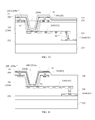
With reference to FIG. 1 and FIG. 9, FIG. 9 illustrates a structural schematic diagram of the non-display area of the array substrate shown in FIG. 1 at a wire changing position of a third metal layer. In the non-display area 20 of the array substrate shown in FIG. 1, the display area 10 and the driving chip IC are provided with a wire changing area 204 therebetween, and the wire changing area 204 is an area where conduction wires of different layers electrically connect with each other so as to change wire. The electrical connection between the third metal layer M3 and the driving chip IC is realized by a wire changing manner. That is, as shown in FIG. 9, the touch electrode line 206 located in the third metal layer M3 will have to change wire by a wire changing electrode block 2042 to be able to electrically connect with the driving lead wire 2044 located in the first metal layer M1, and the driving lead wire 2044 is electrically connected with the driving chip IC directly. It should be noted that, FIG. 9 merely illustrates an embodiment of the present disclosure, in other embodiments, the driving lead wire 2044 directly and electrically connected with the driving chip IC can also be located in the second metal layer M2; or the driving lead wire 2044 is not electrically connected with the driving chip IC, but is directly and electrically connected with the flexible circuit board.
The wire changing manner of touch electrode line 206 can refer to FIG. 10. FIG. 10 illustrates a cross-sectional structural schematic diagram along CC′ in FIG. 9. The connection manner between the third metal layer M3 and the second metal layer M2 shown in FIG. 10 is the same as that shown in FIG. 5, which is not repeated herein. As shown in FIG. 10, the connecting conductor 208 a located in the first oxide conductor layer OC1 is connected with the touch electrode line 206 located in the third metal layer M3 through the first via-hole h1, and the connecting conductor 208 a located in the first oxide conductor layer OC1 is connected with the wire changing electrode block 2042 located in the second metal layer through the second via-hole h2. The first via-hole h1 extends through the third insulation layer 228, and the second via-hole h2 extends through the second insulation layer 226 and the third insulation layer 228. The touch electrode line 206 is electrically connected with the wire changing electrode block 2042 in the above described manner, the wire changing electrode block 2042 located in the second metal layer M2 is electrically connected with the driving lead wire 2044 located in the first metal layer M1 through a fifth via-hole h5, so as to realize the electrical connection between the touch electrode line 206 located in the third metal layer M3 with the driving lead wire 2044 located in the first metal layer M1. It should be noted that, the fourth insulation layer 229 is placed at a side of the connecting conductor 208 a away from the base substrate 220. In the present embodiment, the electrical connection between the touch electrode line 206 and the wire changing electrode block 2042 is realized by the connecting conductor 208 a located at a side of the fourth insulation layer 229 close to the base substrate 220, which prevents the connecting conductor 208 a from being corroded in the subsequent processing procedures, thereby improving stability of the electrical connection between the touch electrode line 206 and the driving chip IC, and thus improving the touch sensitivity.
Optionally, the wire changing manner of the touch electrode line 206 can also refer to FIG. 11. FIG. 11 illustrates another cross-sectional structural schematic diagram along CC′ in FIG. 9. The connection manner between the third metal layer M3 and the second metal layer M2 in FIG. 11 is the same as that shown in FIG. 6, the similar arrangement is not repeated herein. As shown in FIG. 11, the connecting conductor 208 a located in the first oxide conductor layer OC1 is connected with the touch electrode line 206 located in the third metal layer M3 through the first via-hole h1, and the connecting conductor 208 a located in the first oxide conductor layer OC1 is connected with the wire changing electrode block 2042 located in the second metal layer through the second via-hole h2. The first via-hole h1 extends through the third insulation layer 228, and the second via-hole h2 extends through the second insulation layer 226 and the third insulation layer 228. The auxiliary connecting conductor 210 a located in the second oxide conductor layer OC2 directly contacts with the connecting conductor 208 a. The touch electrode line 206 is electrically connected with the wire changing electrode block 2042 in the above described manner, and the wire changing electrode block 2042 located in the second metal layer M2 is electrically connected with the driving lead wire 2044 located in the first metal layer M1 through the fifth via-hole h5, so as to realize the electrical connection between the touch electrode line 206 located in the third metal layer M3 and the driving lead wire 2044 located in the first metal layer M1. In the present embodiment, the stability of the electrical connection between the touch electrode line 206 and the driving chip IC is improved in a way that the auxiliary connecting conductor 210 a directly contacts with the connecting conductor 208 a, thereby improving the touch sensitivity.
It should be noted that, FIG. 11 merely illustrates a partial configuration of the array substrate placed by the present embodiment. In the display area of the array substrate, an insulation layer is placed between the first oxide conductor layer OC1 and the second oxide conductor layer OC2. For example, as shown in FIG. 2 or FIG. 3, the first oxide conductor layer OC1 and the second oxide conductor layer OC2 are provided a fourth insulation layer 229 therebetween. Similarly, in the non-display area, beside the area shown in FIG. 10, other areas of the non-display area can also be provided with the fourth insulation layer 229 between the first oxide conductor layer OC1 and the second oxide conductor layer OC2. Then, the area having an insulation layer between the first oxide conductor layer OC1 and the second oxide conductor layer OC2 can be referred to as a first area, and the area without an insulation layer between the first oxide conductor layer OC1 and the second oxide conductor layer OC2 can be referred to as a second area. The auxiliary connecting conductor 210 a and the connecting conductor 208 a are located in the second area, and an orthogonal projection of the second area on the base substrate 220 overlaps with an orthogonal projection of the through-hole 2264 a defined in the planarization layer 2264 on the base substrate 220.
Optionally, the wire changing manner of the touch electrode line 206 can refer to FIG. 12 and FIG. 13. FIG. 12 illustrates another structural schematic diagram of the non-display area of the array substrate shown in FIG. 1 at a wire changing position of a third metal layer. FIG. 13 illustrates a cross-sectional structural schematic diagram along DD′ in FIG. 12. The connection manner between the third metal layer M3 and the second metal layer M2 shown in FIG. 13 is the same as that shown in FIG. 8, the similar configuration of which is not repeated herein. As shown in FIG. 13, the connecting conductor 208 a located in the first oxide conductor layer OC1 is connected with the touch electrode line 206 located in the third metal layer M3 through the first via-hole h1, and is connected with the wire changing electrode block 2042 located in the second metal layer M2 through the second via-hole h2. The auxiliary connecting conductor 210 a located in the second oxide conductor layer OC2 is connected with the touch electrode line 206 located in the third metal layer M3 through the third via-hole h3, and is connected with the wire changing electrode block 2042 located in the second metal layer M2 through the fourth via-hole h4. The fourth insulation layer 229 is placed between the connecting conductor 208 a and the auxiliary connecting conductor 210 a. The touch electrode line 206 is electrically connected with the wire changing electrode block 2042 in the above-described manner, and the wire changing electrode block 2042 located in the second metal layer M2 is electrically connected with the driving lead wire 2044 located in the first metal layer M1 through the fifth via-hole h5, so as to realize the electrical connection between the touch electrode line 206 located in the third metal layer M3 and the driving lead wire 2044 located in the first metal layer M1. In the present embodiment, the connecting conductor 208 a located in the first oxide conductor layer OC1 and the auxiliary connecting conductor 210 a located in the second oxide conductor layer OC2 are used to connect with the touch electrode line 206 located in the third metal layer M3, and the wire changing electrode block 2042 located in the second metal layer M2, respectively. The connecting conductor 208 a is protected by the fourth insulation layer 229 so as to avoid corrosion in the subsequent processing procedures while the auxiliary connecting conductor 210 a enhances the stability of the electrical connection, thereby further improving the touch sensitivity of the array substrate.
The above-described embodiment is exemplarily illustrated by a situation that the second insulation layer 226 merely includes the planarization layer 2264, however, the embodiment is not limited thereto. In other embodiments, the second insulation layer 226 may include both the planarization layer 2264 and other interbedded insulation layer. The connection manner between the touch electrode line and the control portion is illustrated as follows as an example.
With reference to FIG. 14, FIG. 14 illustrates another cross-sectional structural schematic diagram along CC′ in FIG. 9. The connection manner between the third metal layer M3 and the second metal layer M2 shown in FIG. 14 is the same as that shown in FIG. 10, the similar configuration of which is not repeated herein. A shown in FIG. 14, the second insulation layer 226 includes a planarization layer 2264, a first interbedded insulation layer 2262 and a second interbedded insulation layer 2266. The first interbedded insulation layer 2262 is located between the second metal layer M2 and the planarization layer 2264, and the second interbedded insulation layer 2266 is located between the planarization layer 2264 and the third metal layer M3. Then, it is necessary for the second via-hole h2 to extend through the first interbedded insulation layer 2262 and the second interbedded insulation layer 2266. Since the through-hole 2264 a of the planarization layer 2264 is formed before the third metal layer M3 is formed, and a part of the second metal layer M2 that needs to be electrically connected with the third metal layer M3 has already been exposed via the through-hole 2264 a, the part of the second metal layer M2 located in the through-hole 2264 a will be corroded when the third metal layer M3 is etched. However, the first interbedded insulation layer 2262 and the second interbedded insulation layer 2266 provided in the present embodiment can prevent the second metal layer M2 from being corroded during etching of the third metal layer, thereby improving the stability of the electrical connection between the third metal layer M3 and the second metal layer M2.
It should be noted that, the structure shown in FIG. 14 is merely exemplary, in other embodiments, the number of the interbedded insulation layer located in the second insulation layer 226 may be one or more, the present disclosure has no limitation thereon, and number of the interbedded insulation layer can be selected according to actual production demands.
It should be noted that, in the structures shown in FIG. 5, FIG. 6, FIG. 8, FIG. 10, FIG. 11 and FIG. 13, the second insulation layer 226 can also include one or more interbedded insulation layer. Regardless of the number of the interbedded insulation layer in the second insulation layer 226 is, it is necessary for the through-hole located between the connecting conductor 208 a and the second metal layer M2 to penetrate through each interbedded insulation layer, and/or, it is necessary for the through-hole located between the auxiliary connecting conductor 210 a and the second metal layer M2 to penetrate through each interbedded insulation layer.
In addition, the wire changing manner of the touch electrode line 206 can also refer to FIG. 15. FIG. 15 illustrates still another structural schematic diagram of the non-display area of the array substrate shown in FIG. 1 at a wire changing position of a third metal layer. It should be noted that, the configuration of the wire changing position shown in FIG. 15 is similar to that shown in FIG. 9, the difference thereof lies in that the wire changing electrode block 2042 is electrically connected with two touch electrode lines 206, and the similar portions are not repeated herein. It should be noted that, in FIG. 15, the two touch electrode lines 206 electrically connected with the wire changing electrode block 2042 are electrically connected with a same touch electrode block (common electrode block) in the display area. In other embodiments, if one touch electrode block is electrically connected with a plurality of touch electrode lines 206, the plurality of touch electrode lines 206 will be electrically connected with a same wire changing electrode block 2042 at the wire changing position.
Similarly, in the above embodiments, the through-hole 2264 a is defined in the planarization layer 2264 of the touch electrode line 206 at the wire changing position. The through-hole 2264 a is different from a deep hole that may penetrate through the planarization layer 2264, other film layer in the second insulation layer 226 and the third insulation layer 228 at the electrical connection of the third metal layer M3 and the second metal layer M2, thereby avoiding the connecting conductor 208 a from crossing the deep hole; and/or, The through-hole 2264 a is different form a deep hole that may penetrate through the planarization layer 2264, other film layer in the second insulation layer 226, the third insulation layer 228 and the fourth insulation layer 229 at the electrical connection position of the third metal layer M3 and the second metal layer M2, thereby avoiding the auxiliary connecting conductor 210 a from crossing the deep hole. Therefore, the array substrate provided by the present embodiment can reduce the probability that the connecting conductor 208 a breaks.
The present disclosure further provides a display device. As shown in FIG. 16, FIG. 16 illustrates a structural schematic diagram of a display device according to an embodiment of the present disclosure. The display device includes a housing 2, a display panel 4, a camera 6 and a signal light 8. The display panel 4 includes the array substrate as described in any of the above-described embodiments. Since the anti-corrosion and the stability of electrical connection between the touch electrode line located in the third metal layer M3 and the second metal layer M2 in the array substrate is improved, the touch sensitivity and service life of the display device is improved accordingly.
The embodiments of the present disclosure are described as above in a progressive way. The detailed description in each embodiment illustrates the differences from other embodiments, and the same or similar features of the embodiments can refer to the embodiments mutually. As for the method disclosed in the embodiment, it is simply illustrated as it corresponds to the disclosed structure, and the details thereof can refer to the description of the structure.
Those skilled in the art can implement and utilize the present disclosure with reference to the embodiments described above. Of course, those skilled in the art can make various modifications to those embodiments, and the general principles of the present disclosure can also be implemented in other embodiments without departing from the spirit and scope of the present disclosure. That is, the present disclosure is not limited to those embodiments, but should be interpreted to have the broadest protection scope in conformity with the principles and innovations disclosed in the present disclosure.

Claims (20)

What is claimed is:
1. An array substrate, comprising:
a base substrate, the base substrate comprising a display area and a non-display area;
a first metal layer, located in the display area and the non-display area;
a second metal layer, located at a side of the first metal layer away from the base substrate;
a third metal layer, located at a side of the second metal layer away from the base substrate;
a first insulation layer, placed between the first metal layer and the second metal layer;
a second insulation layer, placed between the second metal layer and the third metal layer;
a first oxide conductor layer, located at a side of the third metal layer away from the base substrate;
a second oxide conductor layer, located at a side of the first oxide conductor layer away from the base substrate;
a third insulation layer, located between the first oxide conductor layer and the third metal layer; and
a fourth insulation layer;
wherein in the display area, the fourth insulation layer is placed between the first oxide conductor layer and the second oxide conductor layer; in the non-display area, the third metal layer is electrically connected with the second metal layer at least by the first oxide conductor layer.
2. The array substrate according to claim 1, wherein the second insulation layer comprises a planarization layer, a through-hole is defined through the planarization layer, an orthogonal projection of the through-hole on the base substrate overlaps an orthogonal projection of the second metal layer on the base substrate.
3. The array substrate according to claim 2, wherein a groove is further defined in the planarization layer.
4. The array substrate according to claim 2, wherein a first via-hole is defined through the third insulation layer, a second via-hole is defined through the second insulation layer and the third insulation layer, an orthogonal projection of the second via-hole on the base substrate overlaps the orthogonal projection of the through-hole defined in the planarization layer on the base substrate, the third metal layer is connected with the first oxide conductor layer through the first via-hole, and the second metal layer is connected with the first oxide conductor layer through the second via-hole.
5. The array substrate according to claim 4, wherein the third metal layer is electrically connected with the second metal layer by the first oxide conductor layer and the second oxide conductor layer.
6. The array substrate according to claim 5, wherein the second oxide conductor layer comprises a first area and a second area;
wherein in the first area, the fourth insulation layer is placed between the second oxide conductor layer and the first oxide conductor layer; in the second area, the second oxide conductor layer contacts the first oxide conductor layer; and an orthogonal projection of the second area on the base substrate overlaps the orthogonal projection of the through-hole defined in the planarization layer on the base substrate.
7. The array substrate according to claim 5, wherein a third via-hole is defined through the fourth insulation layer and the third insulation layer, a fourth via-hole is defined through the fourth insulation layer, the third insulation layer and the second insulation layer, and an orthogonal projection of the fourth via-hole on the base substrate overlaps the orthogonal projection of the through-hole defined in planarization layer on the base substrate; the fourth insulation layer is further placed in the non-display area, the second oxide conductor layer is connected with the third metal layer through the third via-hole, and the second oxide conductor layer is connected with the second metal layer through the fourth via-hole.
8. The array substrate according to claim 1, further comprising:
a plurality of display thin-film transistors in the display area,
a plurality of data lines in the display area,
a plurality of gate lines in the display area, and
a plurality of touch electrode lines in the display area;
wherein the display thin-film transistor comprises a gate electrode, and a source electrode, and a drain electrode; the gate electrode of the display thin-film transistor and the plurality of gate lines are placed in the first metal layer, the source electrode, the drain electrode and the plurality of data lines are placed in the second metal layer, and the plurality of touch electrode lines is placed in the third metal layer.
9. The array substrate according to claim 2, further comprising:
a plurality of display thin-film transistors in the display area,
a plurality of data lines in the display area,
a plurality of gate lines in the display area, and
a plurality of touch electrode lines in the display area;
wherein the display thin-film transistor comprises a gate electrode, and a source electrode, and a drain electrode; the gate electrode of the display thin-film transistor and the plurality of gate lines are placed in the first metal layer, the source electrode, the drain electrode and the plurality of data lines are placed in the second metal layer, and the plurality of touch electrode lines is placed in the third metal layer.
10. The array substrate according to claim 3, further comprising:
a plurality of display thin-film transistors in the display area,
a plurality of data lines in the display area,
a plurality of gate lines in the display area, and
a plurality of touch electrode lines in the display area;
wherein the display thin-film transistor comprises a gate electrode, and a source electrode, and a drain electrode; the gate electrode of the display thin-film transistor and the plurality of gate lines are placed in the first metal layer, the source electrode, the drain electrode and the plurality of data lines are placed in the second metal layer, and the plurality of touch electrode lines is placed in the third metal layer.
11. The array substrate according to claim 4, further comprising:
a plurality of display thin-film transistors in the display area,
a plurality of data lines in the display area,
a plurality of gate lines in the display area, and
a plurality of touch electrode lines in the display area;
wherein the display thin-film transistor comprises a gate electrode, and a source electrode, and a drain electrode; the gate electrode of the display thin-film transistor and the plurality of gate lines are placed in the first metal layer, the source electrode, the drain electrode and the plurality of data lines are placed in the second metal layer, and the plurality of touch electrode lines is placed in the third metal layer.
12. The array substrate according to claim 8, wherein the first oxide conductor layer serves as a pixel electrode and the second oxide conductor layer serves as a common electrode; or the first oxide conductor layer serves as a common electrode and the second oxide conductor layer serves as a pixel electrode.
13. The array substrate according to claim 12, wherein the common electrode is further used as a touch electrode and the touch electrode is electrically connected with the plurality of touch electrode lines in the display area.
14. The array substrate according to claim 1, further comprising an antistatic circuit placed in the non-display area, wherein the antistatic circuit comprises an antistatic thin-film transistor, the antistatic thin-film transistor comprises a gate electrode, a source electrode, and a drain electrode, the gate electrode of the antistatic thin-film transistor is placed in the first metal layer, and the source electrode and the drain electrode of the antistatic thin-film transistor are placed in the second metal layer.
15. The array substrate according to claim 2, further comprising an antistatic circuit placed in the non-display area, wherein the antistatic circuit comprises an antistatic thin-film transistor, the antistatic thin-film transistor comprises a gate electrode, a source electrode, and a drain electrode, the gate electrode of the antistatic thin-film transistor is placed in the first metal layer, and the source electrode and the drain electrode of the antistatic thin-film transistor are placed in the second metal layer.
16. The array substrate according to claim 3, further comprising an antistatic circuit placed in the non-display area, wherein the antistatic circuit comprises an antistatic thin-film transistor, the antistatic thin-film transistor comprises a gate electrode, a source electrode, and a drain electrode, the gate electrode of the antistatic thin-film transistor is placed in the first metal layer, and the source electrode and the drain electrode of the antistatic thin-film transistor are placed in the second metal layer.
17. The array substrate according to claim 4, further comprising an antistatic circuit placed in the non-display area, wherein the antistatic circuit comprises an antistatic thin-film transistor, the antistatic thin-film transistor comprises a gate electrode, a source electrode, and a drain electrode, the gate electrode of the antistatic thin-film transistor is placed in the first metal layer, and the source electrode and the drain electrode of the antistatic thin-film transistor are placed in the second metal layer.
18. The array substrate according to claim 1, further comprising:
a control portion located in the non-display area;
wherein each of the first metal layer, the second metal and the third metal layer is electrically connected with the control portion.
19. The array substrate according to claim 18, wherein the third metal layer is electrically connected with the control portion by the second metal layer and the first metal layer; wherein the third metal layer is electrically connected with the second metal layer, and the second metal layer is electrically connected with the first metal layer through a fifth via-hole.
20. A display device, comprising an array substrate according, wherein the array substrate comprises:
a base substrate, the base substrate comprising a display area and a non-display area;
a first metal layer, located in the display area and the non-display area;
a second metal layer, located at a side of the first metal layer away from the base substrate;
a third metal layer, located at a side of the second metal layer away from the base substrate;
a first insulation layer, placed between the first metal layer and the second metal layer;
a second insulation layer, placed between the second metal layer and the third metal layer;
a first oxide conductor layer, located at a side of the third metal layer away from the base substrate;
a second oxide conductor layer, located at a side of the first oxide conductor layer away from the base substrate;
a third insulation layer, located between the first oxide conductor layer and the third metal layer; and
a fourth insulation layer;
wherein in the display area, the fourth insulation layer is placed between the first oxide conductor layer and the second oxide conductor layer; in the non-display area, the third metal layer is electrically connected with the second metal layer at least by the first oxide conductor layer.
US15/798,859 2017-04-28 2017-10-31 Array substrate and display device including the same Active 2038-03-01 US10409121B2 (en)

Applications Claiming Priority (3)

Application Number Priority Date Filing Date Title
CN201710295964.7A CN106896609B (en) 2017-04-28 2017-04-28 A kind of array substrate and the display device including it
CN201710295964 2017-04-28
CN201710295964.7 2017-04-28

Publications (2)

Publication Number Publication Date
US20180314120A1 US20180314120A1 (en) 2018-11-01
US10409121B2 true US10409121B2 (en) 2019-09-10

Family

ID=59197240

Family Applications (1)

Application Number Title Priority Date Filing Date
US15/798,859 Active 2038-03-01 US10409121B2 (en) 2017-04-28 2017-10-31 Array substrate and display device including the same

Country Status (2)

Country Link
US (1) US10409121B2 (en)
CN (1) CN106896609B (en)

Cited By (2)

* Cited by examiner, † Cited by third party
Publication number Priority date Publication date Assignee Title
US11024695B2 (en) * 2019-05-21 2021-06-01 Shanghai Tianma AM-OLED Co., Ltd. Display panel and display apparatus including the same
US20220115280A1 (en) * 2020-05-12 2022-04-14 Chengdu Boe Optoelectronics Technology Co., Ltd. Display panel and display apparatus

Families Citing this family (19)

* Cited by examiner, † Cited by third party
Publication number Priority date Publication date Assignee Title
KR102580063B1 (en) * 2016-07-21 2023-09-19 삼성디스플레이 주식회사 Display device and method for fabricating the same
JP2018120018A (en) * 2017-01-23 2018-08-02 株式会社ジャパンディスプレイ Display
KR102158204B1 (en) * 2017-08-24 2020-09-22 동우 화인켐 주식회사 Film antenna and display device including the same
CN107561758B (en) * 2017-09-19 2020-03-06 惠科股份有限公司 Touch control display device
CN107807467B (en) * 2017-11-07 2023-08-22 深圳市华星光电半导体显示技术有限公司 Structure for preventing panel peripheral wiring from electrostatic injury
KR102423865B1 (en) * 2017-12-04 2022-07-21 엘지디스플레이 주식회사 Display device having touch sensor
WO2019186652A1 (en) * 2018-03-26 2019-10-03 シャープ株式会社 Method for manufacturing display device and display device
CN108873515B (en) * 2018-06-19 2021-04-02 厦门天马微电子有限公司 Display panel and display device
CN109037235B (en) * 2018-07-20 2021-05-28 Tcl华星光电技术有限公司 Array substrate and manufacturing method thereof
CN108766249B (en) * 2018-08-09 2020-12-29 武汉天马微电子有限公司 Foldable display panel and foldable display device
US11852938B2 (en) * 2018-08-21 2023-12-26 Apple Inc. Displays with data lines that accommodate openings
US10852607B2 (en) * 2018-08-21 2020-12-01 Apple Inc. Displays with data lines that accommodate openings
CN109375405B (en) * 2018-11-30 2021-06-18 厦门天马微电子有限公司 Display panel, manufacturing method thereof and display device
CN112051690B (en) * 2019-06-07 2023-12-22 夏普株式会社 Active matrix substrate and liquid crystal display device with touch sensor
CN110993650B (en) * 2019-11-19 2022-10-04 昆山国显光电有限公司 Display substrate, display device and preparation method of display substrate
CN111916488A (en) * 2020-09-11 2020-11-10 京东方科技集团股份有限公司 Display substrate and display device
CN112799540B (en) * 2021-02-02 2022-05-13 业成科技(成都)有限公司 Touch sensing module, touch display device and manufacturing method thereof
CN113078198B (en) * 2021-03-29 2022-10-25 京东方科技集团股份有限公司 Display substrate and display device
CN113805393A (en) * 2021-08-25 2021-12-17 武汉华星光电技术有限公司 Display panel and electronic terminal

Citations (4)

* Cited by examiner, † Cited by third party
Publication number Priority date Publication date Assignee Title
CN102411238A (en) 2010-09-20 2012-04-11 乐金显示有限公司 Liquid crystal display device and method for manufacturing the same
CN102750024A (en) 2011-04-21 2012-10-24 乐金显示有限公司 Substrate for in-cell type touch sensor liquid crystal display device and method of fabricating the same
US20140160066A1 (en) * 2012-12-11 2014-06-12 Lg Display Co., Ltd. Touch sensor integrated type display device and method of manufacturing the same
US20160026044A1 (en) * 2014-07-25 2016-01-28 Lg Display Co., Ltd. Display device and method of manufacturing the same

Family Cites Families (2)

* Cited by examiner, † Cited by third party
Publication number Priority date Publication date Assignee Title
KR101273239B1 (en) * 2010-09-20 2013-06-11 엘지디스플레이 주식회사 Liquid crystal display device with a built-in touch screen and method for manufacturing the same
CN106033765B (en) * 2015-03-17 2019-06-11 上海和辉光电有限公司 Organic Light Emitting Diode touch-control display panel

Patent Citations (4)

* Cited by examiner, † Cited by third party
Publication number Priority date Publication date Assignee Title
CN102411238A (en) 2010-09-20 2012-04-11 乐金显示有限公司 Liquid crystal display device and method for manufacturing the same
CN102750024A (en) 2011-04-21 2012-10-24 乐金显示有限公司 Substrate for in-cell type touch sensor liquid crystal display device and method of fabricating the same
US20140160066A1 (en) * 2012-12-11 2014-06-12 Lg Display Co., Ltd. Touch sensor integrated type display device and method of manufacturing the same
US20160026044A1 (en) * 2014-07-25 2016-01-28 Lg Display Co., Ltd. Display device and method of manufacturing the same

Non-Patent Citations (1)

* Cited by examiner, † Cited by third party
Title
Chinese OA dated Mar. 19, 2019 for corresponding CN Application No. 201710295964.7.

Cited By (5)

* Cited by examiner, † Cited by third party
Publication number Priority date Publication date Assignee Title
US11024695B2 (en) * 2019-05-21 2021-06-01 Shanghai Tianma AM-OLED Co., Ltd. Display panel and display apparatus including the same
US20210242293A1 (en) * 2019-05-21 2021-08-05 Shanghai Tianma Am-Oled Co.,Ltd. Display panel and display apparatus including the same
US11744122B2 (en) * 2019-05-21 2023-08-29 Shanghai Tianma AM-OLED Co., Ltd. Display panel and display apparatus including the same
US20220115280A1 (en) * 2020-05-12 2022-04-14 Chengdu Boe Optoelectronics Technology Co., Ltd. Display panel and display apparatus
US11728228B2 (en) * 2020-05-12 2023-08-15 Chengdu Boe Optoelectronics Technology Co., Ltd. Display panel and display apparatus

Also Published As

Publication number Publication date
US20180314120A1 (en) 2018-11-01
CN106896609B (en) 2019-11-19
CN106896609A (en) 2017-06-27

Similar Documents

Publication Publication Date Title
US10409121B2 (en) Array substrate and display device including the same
US11437463B2 (en) Display device
US9524992B2 (en) Thin film transistor array panel and manufacturing method thereof
CN106773424B (en) Display panel and display device
EP3088951B1 (en) Array substrate, preparation method thereof, motherboard comprising array substrate and display apparatus
US20160372490A1 (en) Array substrate and manufacturing method thereof, and display panel
KR101601059B1 (en) In-plane switching mode liquid crystal display device
US9647243B2 (en) Display apparatus and method of manufacturing the same
CN107065287B (en) Display panel and display device
KR101668166B1 (en) Array substrate, display device and manufacturing method of array substrate
US9472582B2 (en) Thin film transistor array panel and manufacturing method thereof
US11287709B2 (en) Active matrix substrate and liquid crystal display device
US10579179B2 (en) Display panel and method for manufacturing the same
CN109597522B (en) Touch array substrate and touch display panel
CN109300995B (en) Thin film transistor, manufacturing method thereof, array substrate and display panel
US11177295B2 (en) Array substrate, manufacturing method thereof and display device
CN104409462A (en) Array substrate, manufacturing method thereof and display device
CN109148485B (en) Array substrate, manufacturing method thereof and display device
CN104716147A (en) TFT array substrate, as well as preparation method and display device thereof
KR101978789B1 (en) Array substrate for display device and method of fabricating the same
CN114063835B (en) Touch display panel
KR101971072B1 (en) Liquid Crystal Display Divice Of Fringe Field Switching advanced horizontal in-plane switching mode
KR102486406B1 (en) Array Substrate For Liquid Crystal Display Device
KR20160074141A (en) Liquid crystal display apparatus
CN116047799A (en) Display substrate, display panel and display device

Legal Events

Date Code Title Description
FEPP Fee payment procedure

Free format text: ENTITY STATUS SET TO UNDISCOUNTED (ORIGINAL EVENT CODE: BIG.); ENTITY STATUS OF PATENT OWNER: LARGE ENTITY

AS Assignment

Owner name: XIAMEN TIANMA MICRO-ELECTRONICS CO., LTD., CHINA

Free format text: ASSIGNMENT OF ASSIGNORS INTEREST;ASSIGNOR:PENG, TAO;REEL/FRAME:044158/0543

Effective date: 20171020

STPP Information on status: patent application and granting procedure in general

Free format text: DOCKETED NEW CASE - READY FOR EXAMINATION

STPP Information on status: patent application and granting procedure in general

Free format text: NOTICE OF ALLOWANCE MAILED -- APPLICATION RECEIVED IN OFFICE OF PUBLICATIONS

STPP Information on status: patent application and granting procedure in general

Free format text: PUBLICATIONS -- ISSUE FEE PAYMENT VERIFIED

STCF Information on status: patent grant

Free format text: PATENTED CASE

MAFP Maintenance fee payment

Free format text: PAYMENT OF MAINTENANCE FEE, 4TH YEAR, LARGE ENTITY (ORIGINAL EVENT CODE: M1551); ENTITY STATUS OF PATENT OWNER: LARGE ENTITY

Year of fee payment: 4