US10409104B2 - Display substrate and display device - Google Patents
Display substrate and display device Download PDFInfo
- Publication number
- US10409104B2 US10409104B2 US15/500,987 US201615500987A US10409104B2 US 10409104 B2 US10409104 B2 US 10409104B2 US 201615500987 A US201615500987 A US 201615500987A US 10409104 B2 US10409104 B2 US 10409104B2
- Authority
- US
- United States
- Prior art keywords
- spacer
- color filter
- display substrate
- color filters
- bending part
- Prior art date
- Legal status (The legal status is an assumption and is not a legal conclusion. Google has not performed a legal analysis and makes no representation as to the accuracy of the status listed.)
- Active, expires
Links
Images


Classifications
-
- G—PHYSICS
- G02—OPTICS
- G02F—OPTICAL DEVICES OR ARRANGEMENTS FOR THE CONTROL OF LIGHT BY MODIFICATION OF THE OPTICAL PROPERTIES OF THE MEDIA OF THE ELEMENTS INVOLVED THEREIN; NON-LINEAR OPTICS; FREQUENCY-CHANGING OF LIGHT; OPTICAL LOGIC ELEMENTS; OPTICAL ANALOGUE/DIGITAL CONVERTERS
- G02F1/00—Devices or arrangements for the control of the intensity, colour, phase, polarisation or direction of light arriving from an independent light source, e.g. switching, gating or modulating; Non-linear optics
- G02F1/01—Devices or arrangements for the control of the intensity, colour, phase, polarisation or direction of light arriving from an independent light source, e.g. switching, gating or modulating; Non-linear optics for the control of the intensity, phase, polarisation or colour
- G02F1/13—Devices or arrangements for the control of the intensity, colour, phase, polarisation or direction of light arriving from an independent light source, e.g. switching, gating or modulating; Non-linear optics for the control of the intensity, phase, polarisation or colour based on liquid crystals, e.g. single liquid crystal display cells
- G02F1/133—Constructional arrangements; Operation of liquid crystal cells; Circuit arrangements
- G02F1/1333—Constructional arrangements; Manufacturing methods
- G02F1/1335—Structural association of cells with optical devices, e.g. polarisers or reflectors
- G02F1/133509—Filters, e.g. light shielding masks
- G02F1/133514—Colour filters
-
- G—PHYSICS
- G02—OPTICS
- G02F—OPTICAL DEVICES OR ARRANGEMENTS FOR THE CONTROL OF LIGHT BY MODIFICATION OF THE OPTICAL PROPERTIES OF THE MEDIA OF THE ELEMENTS INVOLVED THEREIN; NON-LINEAR OPTICS; FREQUENCY-CHANGING OF LIGHT; OPTICAL LOGIC ELEMENTS; OPTICAL ANALOGUE/DIGITAL CONVERTERS
- G02F1/00—Devices or arrangements for the control of the intensity, colour, phase, polarisation or direction of light arriving from an independent light source, e.g. switching, gating or modulating; Non-linear optics
- G02F1/01—Devices or arrangements for the control of the intensity, colour, phase, polarisation or direction of light arriving from an independent light source, e.g. switching, gating or modulating; Non-linear optics for the control of the intensity, phase, polarisation or colour
- G02F1/13—Devices or arrangements for the control of the intensity, colour, phase, polarisation or direction of light arriving from an independent light source, e.g. switching, gating or modulating; Non-linear optics for the control of the intensity, phase, polarisation or colour based on liquid crystals, e.g. single liquid crystal display cells
- G02F1/133—Constructional arrangements; Operation of liquid crystal cells; Circuit arrangements
- G02F1/1333—Constructional arrangements; Manufacturing methods
- G02F1/133305—Flexible substrates, e.g. plastics, organic film
-
- G—PHYSICS
- G02—OPTICS
- G02F—OPTICAL DEVICES OR ARRANGEMENTS FOR THE CONTROL OF LIGHT BY MODIFICATION OF THE OPTICAL PROPERTIES OF THE MEDIA OF THE ELEMENTS INVOLVED THEREIN; NON-LINEAR OPTICS; FREQUENCY-CHANGING OF LIGHT; OPTICAL LOGIC ELEMENTS; OPTICAL ANALOGUE/DIGITAL CONVERTERS
- G02F1/00—Devices or arrangements for the control of the intensity, colour, phase, polarisation or direction of light arriving from an independent light source, e.g. switching, gating or modulating; Non-linear optics
- G02F1/01—Devices or arrangements for the control of the intensity, colour, phase, polarisation or direction of light arriving from an independent light source, e.g. switching, gating or modulating; Non-linear optics for the control of the intensity, phase, polarisation or colour
- G02F1/13—Devices or arrangements for the control of the intensity, colour, phase, polarisation or direction of light arriving from an independent light source, e.g. switching, gating or modulating; Non-linear optics for the control of the intensity, phase, polarisation or colour based on liquid crystals, e.g. single liquid crystal display cells
- G02F1/133—Constructional arrangements; Operation of liquid crystal cells; Circuit arrangements
- G02F1/1333—Constructional arrangements; Manufacturing methods
- G02F1/1339—Gaskets; Spacers; Sealing of cells
- G02F1/13394—Gaskets; Spacers; Sealing of cells spacers regularly patterned on the cell subtrate, e.g. walls, pillars
-
- G—PHYSICS
- G02—OPTICS
- G02F—OPTICAL DEVICES OR ARRANGEMENTS FOR THE CONTROL OF LIGHT BY MODIFICATION OF THE OPTICAL PROPERTIES OF THE MEDIA OF THE ELEMENTS INVOLVED THEREIN; NON-LINEAR OPTICS; FREQUENCY-CHANGING OF LIGHT; OPTICAL LOGIC ELEMENTS; OPTICAL ANALOGUE/DIGITAL CONVERTERS
- G02F1/00—Devices or arrangements for the control of the intensity, colour, phase, polarisation or direction of light arriving from an independent light source, e.g. switching, gating or modulating; Non-linear optics
- G02F1/01—Devices or arrangements for the control of the intensity, colour, phase, polarisation or direction of light arriving from an independent light source, e.g. switching, gating or modulating; Non-linear optics for the control of the intensity, phase, polarisation or colour
- G02F1/13—Devices or arrangements for the control of the intensity, colour, phase, polarisation or direction of light arriving from an independent light source, e.g. switching, gating or modulating; Non-linear optics for the control of the intensity, phase, polarisation or colour based on liquid crystals, e.g. single liquid crystal display cells
- G02F1/133—Constructional arrangements; Operation of liquid crystal cells; Circuit arrangements
- G02F1/1333—Constructional arrangements; Manufacturing methods
- G02F1/1339—Gaskets; Spacers; Sealing of cells
- G02F1/13396—Spacers having different sizes
-
- G02F2001/13396—
Definitions
- the present disclosure relates to the field of display technologies, and in particular, to a display substrate and a display device.
- a liquid crystal display device generally comprises an array substrate and a color film substrate, which are cassette-to-cassette packaged and are kept at a distance by a spacer.
- the array substrate is used for implementing the control of luminous brightness
- the color film substrate generally comprises a base and a color filter formed on the base.
- an embodiment of the present disclosure provides a display substrate comprising: a base and multiple color filters and spacers formed on the base. At a position corresponding to at least one spacer, at least one of two adjacent color filters has a bending part at an adjacent border close to the other color filter; wherein at least one bending part is a protrusion adapted to cause a spacer to be located inside the border of a corresponding color filter as a whole, and projection of the bottom surface of the spacer on the side close to the base on the base does not overlap projection of any of the borders of the two adjacent color filters on the base.
- the spacer is at least partially located inside the bending part which is the protrusion.
- each of the two adjacent color filters has the bending part at an adjacent border close to the other color filter; the bending part corresponding to each of the color filters is a protrusion and overlaps the other, and the projection of the bottom surface of the corresponding spacer on the side close to the base on the base is inside a border of a projection of the overlapping part of the two adjacent color filters on the base.
- each of the two color filters has the bending part at an adjacent border close to the other color filter; the bending part corresponding to one of the color filters is the protrusion; and the bending part corresponding to the other color filter is a recess.
- a first color filter in the two color filters has the bending part at an adjacent border close to a second color filter, and the bending part is the protrusion; the second color filter does not have the bending part at an adjacent border close to the first color filter; and the first color filter is any one of the two color filters, and the second color filter is the other one of the two color filters.
- the two adjacent color filters overlap at a position of the bending part, and projection of the bottom surface of the spacer on the side close to the base on the base is outside a border of the projection of overlapping part of the two adjacent color filters on the base.
- the two adjacent color filters do not overlap at a position of the bending part.
- the outline of the bending part is an arc, a polyline, and alternatively a combination of an arc and a polyline.
- one part of the corresponding spacer is located on the protrusion, and the other part is located on body part of a color filter which the protrusion belongs to.
- the spacer is a primary spacer and alternatively an auxiliary spacer, and a shape of an outline of the bending part is the same as that of an outline of a surface of the spacer facing a color filter at a position of the bending part.
- shapes of borders of the individual color filters on a first side are the same; and shapes of borders on a second side are also the same; shapes of borders of the same column of the color filters on the first side at a position of individual rows of pixels are the same, and shapes of borders on the second side at a position of individual rows of pixels are the same.
- an embodiment of the present disclosure provides a display device comprising a display substrate as described in any of the above examples.
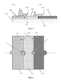
- FIG. 1 is a schematic top view of a display substrate provided by Embodiment One of the disclosure.
- FIG. 2 is a schematic longitudinal section view of the display substrate provided by Embodiment One of the disclosure.
- FIG. 3 is a schematic top view of a display substrate provided by Embodiment Two of the disclosure.
- FIG. 4 is a schematic longitudinal section view of a display substrate provided by Embodiment Three of the disclosure.
- FIG. 5 is a schematic top view of the display substrate provided by Embodiment Three of the disclosure.
- FIG. 6 is a schematic longitudinal section view of a display substrate provided by Embodiment Four of the disclosure.
- FIG. 7 is a schematic top view of the display substrate provided by Embodiment Four of the disclosure.
- An embodiment of the present disclosure provides a display substrate, the display substrate comprising a base and multiple color filters and spaces formed on the base; at a position corresponding to at least one spacer, at least one of two adjacent color filters having a bending part at an adjacent border close to the other color filter; wherein at least one bending part is a protrusion adapted to cause a spacer to be located inside the border of a corresponding color filter as a whole, and projection of the bottom surface of the spacer on the side close to the base on the base does not overlap projection of any of borders of the two adjacent color filters on the base.
- the borders of two adjacent color filters are not under the spacer, such that the region corresponding to the spacer is flat as a whole, which is conducive to stable arrangement of the spacer.
- the border may in particular refer to a border in the column direction
- the column direction is consistent with the understanding in the prior art, that is, after the display substrate is applied in a corresponding display device, the direction perpendicular to the extending direction of a grid line of the display device, namely, the direction in which a data line extends.
- the bending part may mean that the corresponding color filter has a protrusion, such that a border of the color filter has a bending part, and alternatively also may mean that the corresponding color filter has a recess, such that a border of the color filter has a bending part.
- the corresponding display device comprises a main spacer and an auxiliary spacer
- “at a position corresponding to a spacer” may refer to at a position corresponding to a main spacer, and alternatively at a position corresponding to an auxiliary spacer.
- two adjacent color filters may have an overlap in the column direction and alternatively also may not have an overlap in the column direction at the position of a spacer.
- FIG. 1 and FIG. 2 for the structure of a display substrate provided by Embodiment One of the disclosure, which comprises a base 100 and a color filter 210 , a color filter 220 , a color filter 230 , a primary spacer A and an auxiliary spacer A′ formed on the base 100 , the color of the color filter 210 , the color of the color filter 220 and the color of the color filter 230 being different; wherein the primary spacer A is arranged at a position where the color filter 210 borders the color filter 220 , and the auxiliary spacer A′ is arranged at a position where the color filter 220 borders the color filter 230 .
- the color filter 210 has a protrusion toward the right side, such that a border L 12 of the color filter 210 in the column direction has a rightward bending part, and the bending part may cause the corresponding primary spacer A to be located inside the border of the color filter 210 as a whole; in addition, at the position of the primary spacer A, the color filter 220 has a recess toward the right side, such that a border L 21 of the color filter 220 in the column direction also has a rightward bending part, which may cause the corresponding primary spacer A to be able to be located outside the border of the color filter 220 as a whole. And the color filter 210 and the color filter 220 have no overlap at the positions of the bending parts.
- a color filter 210 under the primary spacer A is only arranged a color filter 210 , and the color filter 210 overspreads the region under the primary spacer A, such that the whole spacer A is arranged on a flat surface, which contributes to the stability of the primary spacer A.
- the color filter 220 has a protrusion toward the right side, such that a border L 23 of the color filter 220 in the column direction has a rightward bending part, and the bending part may cause the corresponding auxiliary spacer A′ to be located inside the border of the color filter 220 as a whole; and at the position of the auxiliary spacer A′, the color filter 230 has a recess toward the right side, such that a border L 32 of the color filter 230 in the column direction also has a rightward bending part, which may cause the corresponding auxiliary spacer A′ to be able to be located outside the border of the color filter 230 as a whole.
- the color filter 220 and the color filter 230 also have no overlap. Since the size of the auxiliary spacer A′ is less than the size of the primary spacer A, the sizes of the bending part in the border L 23 and the bending part in the border L 32 are less than those of the bending part in the border L 12 and the bending part in the border L 21 .
- a color filter 220 at the position corresponding to the auxiliary spacer A′, on a surface of the display substrate facing the auxiliary spacer A′ is only arranged a color filter 220 , and material of the color filter 220 overspreads the region under the whole auxiliary spacer A′, such that the whole auxiliary spacer A′ is arranged on a flat surface, which contributes to the stability of the auxiliary spacer A′.
- the shape of an individual bending part is a semicircular arc, and is identical to the outline of the bottom surface of a spacer (i.e., a surface facing a color filter when arranged on the color filter) at the bending part, which may thus reduce the size of the bending part as much as possible and facilitate the design and layout of the color filter.
- a bending part herein may also be a square consisting of multiple polylines.
- an outline of an individual bending part may also be of another shape, for example, a combination of polylines and arcs.
- one part of a spacer is located on the protrusion, and the other part is located on body part of a corresponding color filter.
- the size of a bending part may also be reduced, and the design and layout of the color filter at the position of the bending part is facilitated.
- FIG. 3 for the structure of a display substrate provided by Embodiment Two of the disclosure.
- the border L 21 in the column direction of the color filter 220 does not have a protrusion and a recess, namely, it does not have a bending part
- the border L 32 in the column direction of the color filter 230 does not have a bending part, either.
- the sectional view at C-C′ of the display substrate provided by Embodiment Two is analogous to FIG. 2 , and will not be described in detail here. At this time, two adjacent color filters do not overlap at the position of the bending part.
- Embodiment Two it is also flat at the position where the spacer is arranged, which may cause the spacer to be arranged stably.
- FIG. 4 and FIG. 5 for the structure of a display substrate provided by Embodiment Three of the disclosure. Unlike Embodiment Two, at the position of the primary spacer A, part of the protrusion of the color filter 210 is stacked above the color filter 220 , and at the position of the auxiliary spacer A′, part of the protrusion of the color filter 220 is stacked above the color filter 230 (in FIG. 4 and FIG. 5 , it is assumed that the color filter 210 is arranged above the color filter 220 , and the color filter 220 is arranged above the color filter 230 ).
- Embodiment Three it is also flat at the position where the spacer is arranged, which may cause the spacer to be arranged stably.
- Embodiment Three reference may be made to the description about Embodiment Two, and they will not be described again here.
- the color filter 220 also has a protrusion toward the left side, such that the color filter 220 has a bending part at a border in the column direction.
- the color filter 230 also has a protrusion toward the left side, such that the color filter 230 has a bending part at a border in the column direction.
- two layers of color filter layer materials overspread a surface of the display substrate facing the spacers (in FIG. 6 and FIG.
- the color filter 210 is arranged above the color filter 220 , and the color filter 220 is arranged above the color filter 230 ), which may thus also cause the surface of the display substrate facing the spacers to be flat and is conducive to stably arranging the spacers.
- the display substrate provided by Embodiment Four it is also flat at the position where the spacer is arranged, which may cause the spacer to be arranged stably.
- the display substrate provided by Embodiment Four reference may be made to the description about Embodiment One, and they will not be described again here.
- bending directions of the bending parts in the borders of two adjacent color filters 220 in the column direction may be the same, for example, as shown in FIG. 1 and FIG. 2 , both are toward the right side shown in the figures (of course, in a practical application, both may be also toward the left side, unnecessarily according to the manner in FIG. 1 and FIG. 2 ), and alternatively the bending directions of the bending parts in the borders of two adjacent color filters 220 in the column direction may be opposite to each other.
- the number of colors of the color filters comprised in the display substrates described above may also not be 3, for example, may be 4, and at this point, colors of the color filters may be RGBW.
- the individual spacers may be distributed along data lines in an array substrate corresponding to the display substrate.
- the display substrate may be arranged according to the following manner: at the position of the same row of pixels, shapes of the borders of the individual color filters in the column direction on a first side are the same; shapes of the borders in the column direction on a second side are also the same; and shapes of the borders of the same column of color filters in the column direction on the first side at the position of an individual row of pixels are the same, and shapes of the borders in the column direction on the second side at the position of an individual row of pixels are also the same.
- the display substrate referred to by the disclosure may particularly refer to a color film substrate, and alternatively also may refer to an array substrate on which color filters are formed. What form is specifically implemented for the above display substrate is not defined by the invention.
- a common electrode layer e.g., a common electrode layer, etc.
- the spacers may be specifically arranged on a corresponding structural layer, but not directly arranged above the color filters.
- the thickness of the common electrode layer is relatively little and uniform, which will not have much impact on the shape of the upper surface of the display substrate.
- the left side direction and the right side direction may be interchanged.
- Embodiment One it may be such that the left sides of the individual color filters have protrusions, and the right sides have recesses; and in Embodiment Two, it may be such that the left sides of the individual color filters have protrusions, and the right sides have no bending parts.
- Embodiment Two it may be such that the left sides of the individual color filters have protrusions, and the right sides have no bending parts.
- the corresponding technical solutions may also achieve the basic object of the embodiments of the present disclosure, and should also fall within the protection scope of the invention.
- the embodiments of the present disclosure further provides a display device comprising a first display substrate, a second display substrate and a liquid crystal layer; the first display substrate and the second display substrate being separated by a spacer, the liquid crystal layer being located between the first display substrate and the second display substrate; wherein the first display substrate is a display substrate as described in any of the above embodiments.
- the display device herein may be any product and alternatively component with the display function, such as electronic paper, a mobile phone, a tablet computer, a TV set, a display, a notebook computer, a digital photo frame, a navigator, etc.
Applications Claiming Priority (3)
| Application Number | Priority Date | Filing Date | Title |
|---|---|---|---|
| CN201620208019U | 2016-03-17 | ||
| CN201620208019.XU CN205427389U (zh) | 2016-03-17 | 2016-03-17 | 显示基板及显示装置 |
| PCT/CN2016/082759 WO2017156861A1 (zh) | 2016-03-17 | 2016-05-20 | 显示基板及显示装置 |
Publications (2)
| Publication Number | Publication Date |
|---|---|
| US20180180934A1 US20180180934A1 (en) | 2018-06-28 |
| US10409104B2 true US10409104B2 (en) | 2019-09-10 |
Family
ID=56520007
Family Applications (1)
| Application Number | Title | Priority Date | Filing Date |
|---|---|---|---|
| US15/500,987 Active 2036-10-18 US10409104B2 (en) | 2016-03-17 | 2016-05-20 | Display substrate and display device |
Country Status (3)
| Country | Link |
|---|---|
| US (1) | US10409104B2 (zh) |
| CN (1) | CN205427389U (zh) |
| WO (1) | WO2017156861A1 (zh) |
Families Citing this family (10)
| Publication number | Priority date | Publication date | Assignee | Title |
|---|---|---|---|---|
| CN108153033A (zh) * | 2016-12-02 | 2018-06-12 | 上海仪电显示材料有限公司 | 滤光片及其制造方法、掩膜版以及液晶显示装置 |
| CN108227273B (zh) * | 2016-12-21 | 2021-03-09 | 上海仪电显示材料有限公司 | 显示面板、彩色滤色基板及彩色滤色基板的制作方法 |
| CN107422408B (zh) * | 2017-08-02 | 2020-03-17 | 深圳市华星光电技术有限公司 | 彩色滤光片及显示面板 |
| CN107340627B (zh) * | 2017-09-01 | 2020-10-09 | 深圳市华星光电技术有限公司 | 曲面液晶面板 |
| US10509280B2 (en) | 2017-09-01 | 2019-12-17 | Shenzhen China Star Optoelectronics Technology Co., Ltd | Liquid crystal panel |
| CN108873449B (zh) * | 2018-06-20 | 2021-05-28 | 昆山龙腾光电股份有限公司 | 彩色滤光基板及液晶显示装置 |
| CN108897163A (zh) * | 2018-09-12 | 2018-11-27 | 惠科股份有限公司 | 显示面板及显示面板的制作方法 |
| CN110543046A (zh) * | 2018-11-26 | 2019-12-06 | 友达光电股份有限公司 | 显示面板 |
| TWI679754B (zh) * | 2018-11-26 | 2019-12-11 | 友達光電股份有限公司 | 元件基板 |
| CN211928360U (zh) * | 2020-05-29 | 2020-11-13 | 北京京东方显示技术有限公司 | 显示装置 |
Citations (7)
| Publication number | Priority date | Publication date | Assignee | Title |
|---|---|---|---|---|
| CN1493901A (zh) | 2002-10-31 | 2004-05-05 | 统宝光电股份有限公司 | 彩色滤光片的结构 |
| US20070182888A1 (en) | 2006-02-03 | 2007-08-09 | Toshiba Matsushita Display Technology Co., Ltd. | Liquid crystal display device |
| CN101587200A (zh) | 2007-12-04 | 2009-11-25 | 友达光电股份有限公司 | 彩色滤光片基板及图案化掩模 |
| US20100002172A1 (en) | 2008-07-01 | 2010-01-07 | Samsung Electronics Co., Ltd. | Liquid crystal display including color filters, and manufacturing method thereof |
| CN102047153A (zh) | 2008-07-15 | 2011-05-04 | 夏普株式会社 | 滤色器基板和液晶显示装置 |
| US20140049717A1 (en) | 2012-08-17 | 2014-02-20 | Samsung Display Co., Ltd. | Liquid crystal display and method for manufacturing the same |
| US20160033814A1 (en) * | 2014-07-30 | 2016-02-04 | Samsung Display Co., Ltd. | Liquid crystal display panel and manufacturing method thereof |
-
2016
- 2016-03-17 CN CN201620208019.XU patent/CN205427389U/zh active Active
- 2016-05-20 US US15/500,987 patent/US10409104B2/en active Active
- 2016-05-20 WO PCT/CN2016/082759 patent/WO2017156861A1/zh active Application Filing
Patent Citations (7)
| Publication number | Priority date | Publication date | Assignee | Title |
|---|---|---|---|---|
| CN1493901A (zh) | 2002-10-31 | 2004-05-05 | 统宝光电股份有限公司 | 彩色滤光片的结构 |
| US20070182888A1 (en) | 2006-02-03 | 2007-08-09 | Toshiba Matsushita Display Technology Co., Ltd. | Liquid crystal display device |
| CN101587200A (zh) | 2007-12-04 | 2009-11-25 | 友达光电股份有限公司 | 彩色滤光片基板及图案化掩模 |
| US20100002172A1 (en) | 2008-07-01 | 2010-01-07 | Samsung Electronics Co., Ltd. | Liquid crystal display including color filters, and manufacturing method thereof |
| CN102047153A (zh) | 2008-07-15 | 2011-05-04 | 夏普株式会社 | 滤色器基板和液晶显示装置 |
| US20140049717A1 (en) | 2012-08-17 | 2014-02-20 | Samsung Display Co., Ltd. | Liquid crystal display and method for manufacturing the same |
| US20160033814A1 (en) * | 2014-07-30 | 2016-02-04 | Samsung Display Co., Ltd. | Liquid crystal display panel and manufacturing method thereof |
Non-Patent Citations (1)
| Title |
|---|
| International Search Report for PCT/CN2016/082759 dated Oct. 20, 2016. |
Also Published As
| Publication number | Publication date |
|---|---|
| US20180180934A1 (en) | 2018-06-28 |
| CN205427389U (zh) | 2016-08-03 |
| WO2017156861A1 (zh) | 2017-09-21 |
Similar Documents
| Publication | Publication Date | Title |
|---|---|---|
| US10409104B2 (en) | Display substrate and display device | |
| US10534461B2 (en) | In-cell touch substrate and method for driving the same, display panel | |
| US9535196B2 (en) | Color filter substrate, method for fabricating the same, display panel and display device | |
| US9349756B2 (en) | Array substrate, display panel and display device | |
| US10409423B2 (en) | Optical touch substrate, in-cell touch panel and display device | |
| CN104020605B (zh) | 显示面板 | |
| US9666146B2 (en) | Display panel of touch screen and electronic device | |
| US9086604B2 (en) | Arrray substrate and display device | |
| WO2020087859A1 (zh) | 显示屏以及显示终端 | |
| US10084028B2 (en) | Method for manufacturing display substrate, display substrate and display device | |
| CN109188751B (zh) | 显示面板、显示装置以及显示面板的制作方法 | |
| US9891461B2 (en) | Display panel, manufacturing method thereof and display device | |
| WO2017004948A1 (zh) | 阵列基板及其制作方法和显示装置 | |
| US20170192316A1 (en) | Array substrate, liquid crystal display panel and display device | |
| JP2019525256A (ja) | 液晶表示パネル及び液晶表示装置 | |
| US20210080791A1 (en) | Display device and display panel thereof, and manufacturing method for display device | |
| JPWO2011132439A1 (ja) | 液晶表示装置 | |
| CN104977749A (zh) | 彩膜基板及其制作方法以及显示装置 | |
| US20170092861A1 (en) | A metal mask plate and an organic electroluminescent display device manufactured using the same | |
| US11573443B2 (en) | Liquid crystal display panel and method for manufacturing same, and liquid crystal display | |
| US10317587B2 (en) | Fabrication method of color filter substrate, color filter substrate and display device | |
| US10914990B2 (en) | Vertical alignment display panel and display apparatus | |
| TWI539217B (zh) | 顯示面板 | |
| TW201602648A (zh) | 顯示面板 | |
| US10481715B2 (en) | Touch assembly, display panel and a method for manufacturing touch assembly |
Legal Events
| Date | Code | Title | Description |
|---|---|---|---|
| AS | Assignment |
Owner name: BOE TECHNOLOGY GROUP CO., LTD., CHINA Free format text: ASSIGNMENT OF ASSIGNORS INTEREST;ASSIGNORS:HU, YONG;WU, XINYIN;REEL/FRAME:041151/0290 Effective date: 20170118 |
|
| STPP | Information on status: patent application and granting procedure in general |
Free format text: ADVISORY ACTION MAILED |
|
| STPP | Information on status: patent application and granting procedure in general |
Free format text: RESPONSE AFTER FINAL ACTION FORWARDED TO EXAMINER |
|
| STPP | Information on status: patent application and granting procedure in general |
Free format text: NOTICE OF ALLOWANCE MAILED -- APPLICATION RECEIVED IN OFFICE OF PUBLICATIONS |
|
| STPP | Information on status: patent application and granting procedure in general |
Free format text: PUBLICATIONS -- ISSUE FEE PAYMENT VERIFIED |
|
| STCF | Information on status: patent grant |
Free format text: PATENTED CASE |
|
| MAFP | Maintenance fee payment |
Free format text: PAYMENT OF MAINTENANCE FEE, 4TH YEAR, LARGE ENTITY (ORIGINAL EVENT CODE: M1551); ENTITY STATUS OF PATENT OWNER: LARGE ENTITY Year of fee payment: 4 |