US10347701B2 - Organic light-emitting display panel, display device and organic light-emitting display motherboard thereof - Google Patents
Organic light-emitting display panel, display device and organic light-emitting display motherboard thereof Download PDFInfo
- Publication number
- US10347701B2 US10347701B2 US15/907,842 US201815907842A US10347701B2 US 10347701 B2 US10347701 B2 US 10347701B2 US 201815907842 A US201815907842 A US 201815907842A US 10347701 B2 US10347701 B2 US 10347701B2
- Authority
- US
- United States
- Prior art keywords
- organic light
- metal wire
- display panel
- emitting display
- metal
- Prior art date
- Legal status (The legal status is an assumption and is not a legal conclusion. Google has not performed a legal analysis and makes no representation as to the accuracy of the status listed.)
- Active
Links
- 229910052751 metal Inorganic materials 0.000 claims abstract description 265
- 239000002184 metal Substances 0.000 claims abstract description 265
- 238000009413 insulation Methods 0.000 claims abstract description 82
- 239000000758 substrate Substances 0.000 claims abstract description 74
- 239000000463 material Substances 0.000 claims abstract description 70
- 229910052709 silver Inorganic materials 0.000 claims abstract description 65
- 239000004332 silver Substances 0.000 claims abstract description 65
- 230000004888 barrier function Effects 0.000 claims description 80
- 125000006850 spacer group Chemical group 0.000 claims description 80
- 239000010409 thin film Substances 0.000 claims description 41
- 238000005538 encapsulation Methods 0.000 claims description 28
- 229910003437 indium oxide Inorganic materials 0.000 claims description 16
- PJXISJQVUVHSOJ-UHFFFAOYSA-N indium(iii) oxide Chemical compound [O-2].[O-2].[O-2].[In+3].[In+3] PJXISJQVUVHSOJ-UHFFFAOYSA-N 0.000 claims description 16
- XAGFODPZIPBFFR-UHFFFAOYSA-N aluminium Chemical compound [Al] XAGFODPZIPBFFR-UHFFFAOYSA-N 0.000 claims description 10
- XOLBLPGZBRYERU-UHFFFAOYSA-N tin dioxide Chemical compound O=[Sn]=O XOLBLPGZBRYERU-UHFFFAOYSA-N 0.000 claims description 10
- XLOMVQKBTHCTTD-UHFFFAOYSA-N Zinc monoxide Chemical compound [Zn]=O XLOMVQKBTHCTTD-UHFFFAOYSA-N 0.000 claims description 9
- 229910052782 aluminium Inorganic materials 0.000 claims description 9
- 239000004065 semiconductor Substances 0.000 claims description 7
- 229910001887 tin oxide Inorganic materials 0.000 claims description 6
- AJNVQOSZGJRYEI-UHFFFAOYSA-N digallium;oxygen(2-) Chemical compound [O-2].[O-2].[O-2].[Ga+3].[Ga+3] AJNVQOSZGJRYEI-UHFFFAOYSA-N 0.000 claims description 5
- 229910044991 metal oxide Inorganic materials 0.000 claims description 5
- 150000004706 metal oxides Chemical class 0.000 claims description 5
- 229910001195 gallium oxide Inorganic materials 0.000 claims description 4
- 239000011787 zinc oxide Substances 0.000 claims description 4
- AMGQUBHHOARCQH-UHFFFAOYSA-N indium;oxotin Chemical compound [In].[Sn]=O AMGQUBHHOARCQH-UHFFFAOYSA-N 0.000 claims description 3
- 238000003466 welding Methods 0.000 claims description 2
- 230000000149 penetrating effect Effects 0.000 abstract description 5
- 239000010410 layer Substances 0.000 description 155
- -1 silver ions Chemical class 0.000 description 34
- 239000002923 metal particle Substances 0.000 description 30
- 238000005530 etching Methods 0.000 description 27
- 239000010408 film Substances 0.000 description 25
- BQCADISMDOOEFD-UHFFFAOYSA-N Silver Chemical compound [Ag] BQCADISMDOOEFD-UHFFFAOYSA-N 0.000 description 22
- 238000004519 manufacturing process Methods 0.000 description 20
- 238000006722 reduction reaction Methods 0.000 description 13
- 230000000694 effects Effects 0.000 description 12
- 238000000034 method Methods 0.000 description 12
- 239000002253 acid Substances 0.000 description 11
- QVGXLLKOCUKJST-UHFFFAOYSA-N atomic oxygen Chemical compound [O] QVGXLLKOCUKJST-UHFFFAOYSA-N 0.000 description 10
- 239000012535 impurity Substances 0.000 description 10
- 239000001301 oxygen Substances 0.000 description 10
- 229910052760 oxygen Inorganic materials 0.000 description 10
- 239000007769 metal material Substances 0.000 description 8
- 230000008569 process Effects 0.000 description 7
- 238000005520 cutting process Methods 0.000 description 5
- 238000010586 diagram Methods 0.000 description 5
- 239000011368 organic material Substances 0.000 description 4
- 238000000059 patterning Methods 0.000 description 4
- 239000007787 solid Substances 0.000 description 4
- 239000000126 substance Substances 0.000 description 4
- 239000010936 titanium Substances 0.000 description 4
- PXHVJJICTQNCMI-UHFFFAOYSA-N Nickel Chemical compound [Ni] PXHVJJICTQNCMI-UHFFFAOYSA-N 0.000 description 3
- RTAQQCXQSZGOHL-UHFFFAOYSA-N Titanium Chemical compound [Ti] RTAQQCXQSZGOHL-UHFFFAOYSA-N 0.000 description 3
- 238000006243 chemical reaction Methods 0.000 description 3
- 229910052719 titanium Inorganic materials 0.000 description 3
- 239000004642 Polyimide Substances 0.000 description 2
- 239000003990 capacitor Substances 0.000 description 2
- 150000001768 cations Chemical class 0.000 description 2
- 239000011651 chromium Substances 0.000 description 2
- 239000010949 copper Substances 0.000 description 2
- 238000005516 engineering process Methods 0.000 description 2
- 239000011521 glass Substances 0.000 description 2
- 229910010272 inorganic material Inorganic materials 0.000 description 2
- 239000011147 inorganic material Substances 0.000 description 2
- 230000003647 oxidation Effects 0.000 description 2
- 238000007254 oxidation reaction Methods 0.000 description 2
- 229920001721 polyimide Polymers 0.000 description 2
- 238000005036 potential barrier Methods 0.000 description 2
- 239000011347 resin Substances 0.000 description 2
- 229920005989 resin Polymers 0.000 description 2
- VYZAMTAEIAYCRO-UHFFFAOYSA-N Chromium Chemical compound [Cr] VYZAMTAEIAYCRO-UHFFFAOYSA-N 0.000 description 1
- RYGMFSIKBFXOCR-UHFFFAOYSA-N Copper Chemical compound [Cu] RYGMFSIKBFXOCR-UHFFFAOYSA-N 0.000 description 1
- XEEYBQQBJWHFJM-UHFFFAOYSA-N Iron Chemical compound [Fe] XEEYBQQBJWHFJM-UHFFFAOYSA-N 0.000 description 1
- ZOKXTWBITQBERF-UHFFFAOYSA-N Molybdenum Chemical compound [Mo] ZOKXTWBITQBERF-UHFFFAOYSA-N 0.000 description 1
- 230000005540 biological transmission Effects 0.000 description 1
- 229910052804 chromium Inorganic materials 0.000 description 1
- 239000003086 colorant Substances 0.000 description 1
- 239000004020 conductor Substances 0.000 description 1
- 229910052802 copper Inorganic materials 0.000 description 1
- 239000003792 electrolyte Substances 0.000 description 1
- 238000011031 large-scale manufacturing process Methods 0.000 description 1
- 229910001092 metal group alloy Inorganic materials 0.000 description 1
- 150000002739 metals Chemical class 0.000 description 1
- 239000000203 mixture Substances 0.000 description 1
- 238000012986 modification Methods 0.000 description 1
- 230000004048 modification Effects 0.000 description 1
- 229910052750 molybdenum Inorganic materials 0.000 description 1
- 239000011733 molybdenum Substances 0.000 description 1
- 229910052759 nickel Inorganic materials 0.000 description 1
- 239000012044 organic layer Substances 0.000 description 1
- 238000001556 precipitation Methods 0.000 description 1
- 239000002994 raw material Substances 0.000 description 1
- 230000004044 response Effects 0.000 description 1
- 238000007740 vapor deposition Methods 0.000 description 1
Images


Classifications
-
- H—ELECTRICITY
- H10—SEMICONDUCTOR DEVICES; ELECTRIC SOLID-STATE DEVICES NOT OTHERWISE PROVIDED FOR
- H10K—ORGANIC ELECTRIC SOLID-STATE DEVICES
- H10K59/00—Integrated devices, or assemblies of multiple devices, comprising at least one organic light-emitting element covered by group H10K50/00
- H10K59/10—OLED displays
- H10K59/12—Active-matrix OLED [AMOLED] displays
- H10K59/131—Interconnections, e.g. wiring lines or terminals
-
- H01L27/3248—
-
- H01L27/3276—
-
- H01L51/5206—
-
- H—ELECTRICITY
- H10—SEMICONDUCTOR DEVICES; ELECTRIC SOLID-STATE DEVICES NOT OTHERWISE PROVIDED FOR
- H10K—ORGANIC ELECTRIC SOLID-STATE DEVICES
- H10K50/00—Organic light-emitting devices
- H10K50/80—Constructional details
- H10K50/805—Electrodes
- H10K50/81—Anodes
-
- H—ELECTRICITY
- H10—SEMICONDUCTOR DEVICES; ELECTRIC SOLID-STATE DEVICES NOT OTHERWISE PROVIDED FOR
- H10K—ORGANIC ELECTRIC SOLID-STATE DEVICES
- H10K59/00—Integrated devices, or assemblies of multiple devices, comprising at least one organic light-emitting element covered by group H10K50/00
- H10K59/10—OLED displays
- H10K59/12—Active-matrix OLED [AMOLED] displays
- H10K59/123—Connection of the pixel electrodes to the thin film transistors [TFT]
-
- H01L2251/55—
-
- H—ELECTRICITY
- H10—SEMICONDUCTOR DEVICES; ELECTRIC SOLID-STATE DEVICES NOT OTHERWISE PROVIDED FOR
- H10K—ORGANIC ELECTRIC SOLID-STATE DEVICES
- H10K2101/00—Properties of the organic materials covered by group H10K85/00
Definitions
- the present disclosure generally relates to the field of display technology and, more particularly, relates to an organic light-emitting display panel, a display device and an organic light-emitting display motherboard thereof.
- An organic light-emitting display panel includes organic light-emitting diodes (OLEDs), and is featured with various advantages, such as self-luminous, wide viewing angle, high contrast, low power consumption and high response speed, etc. Thus, organic light-emitting display panels are increasingly favored by consumers.
- OLEDs organic light-emitting diodes
- organic light-emitting display panels are highly desired to be improved.
- the disclosed organic light-emitting display panel and device are directed to solve one or more problems set forth above and other problems.
- the organic light-emitting display panel comprises a base substrate, and a metal wire disposed on the base substrate.
- the metal wire has a first surface facing the base substrate and an opposing second surface, and the opposing second surface is an upper surface of the metal wire.
- a material of the metal wire includes a first metal.
- the organic light-emitting display panel also includes a first insulation layer covering the upper surface of the metal wire.
- the first insulation layer includes at least one hollow portion, and the at least one hollow portion penetrates through the first insulation layer along a thickness direction of the first insulation layer and exposes a portion of the upper surface of the metal wire.
- the organic light-emitting display panel includes a conductive portion disposed on the upper surface of the metal wire. Along a direction perpendicular to the base substrate, the conductive portion is not overlapped with the at least one hollow portion, and the conductive portion is electrically connected to the metal wire.
- a work function of a material of the conductive portion is G1
- a work function of metal silver is G2
- a work function of the first metal is G3, and G1>G2>G3.
- the display device comprises an organic light-emitting display panel.
- the organic light-emitting display panel includes a base substrate, and a metal wire disposed on the base substrate.
- the metal wire has a first surface facing the base substrate and an opposing second surface, and the opposing second surface is an upper surface of the metal wire.
- a material of the metal wire includes a first metal.
- the organic light-emitting display panel also includes a first insulation layer covering the upper surface of the metal wire.
- the first insulation layer includes at least one hollow portion, and the at least one hollow portion penetrates through the first insulation layer along a thickness direction of the first insulation layer and exposes a portion of the upper surface of the metal wire.
- the organic light-emitting display panel includes a conductive portion disposed on the upper surface of the metal wire. Along a direction perpendicular to the base substrate, the conductive portion is not overlapped with the at least one hollow portion, and the conductive portion is electrically connected to the metal wire.
- a work function of a material of the conductive portion is G1
- a work function of metal silver is G2
- a work function of the first metal is G3, and G1>G2>G3.
- the organic light-emitting display motherboard comprises a mother base substrate, and a metal wire disposed on the mother base substrate.
- the metal wire has a first surface facing the mother base substrate and an opposing second surface, and the opposing second surface is an upper surface of the metal wire.
- a material of the metal wire includes a first metal.
- the organic light-emitting display motherboard also includes a first insulation layer covering the upper surface of the metal wire.
- the first insulation layer includes at least one hollow portion, and the at least one hollow portion penetrates through the first insulation layer along a thickness direction of the first insulation layer and exposes a portion of the upper surface of the metal wire.
- the organic light-emitting display motherboard includes a conductive portion disposed on the upper surface of the metal wire. Along a direction perpendicular to the mother base substrate, the conductive portion is not overlapped with the at least one hollow portion, and the conductive portion is electrically connected to the metal wire.
- a work function of a material of the conductive portion is G1
- a work function of metal silver is G2
- a work function of the first metal is G3, and G1>G2>G3.
- the organic light-emitting display motherboard includes a plurality of sub-display panel regions, wherein the conductive portion is disposed in a region other than a sub-display panel region.
- FIG. 1 illustrates a schematic local cross-sectional view of an exemplary organic light-emitting display panel consistent with disclosed embodiments of the present disclosure
- FIG. 2 illustrates a schematic local cross-sectional view of another exemplary organic light-emitting display panel consistent with disclosed embodiments of the present disclosure
- FIG. 3 illustrates a schematic local cross-sectional view of another exemplary organic light-emitting display panel consistent with disclosed embodiments of the present disclosure
- FIG. 4 illustrates a circuit diagram of an exemplary pixel circuit in an exemplary organic light-emitting display panel consistent with disclosed embodiments of the present disclosure
- FIG. 5 illustrates a schematic top view of an exemplary organic light-emitting display panel consistent with disclosed embodiments of the present disclosure
- FIG. 6 illustrates a schematic CC′-sectional view of an exemplary organic light-emitting display panel in FIG. 5 consistent with disclosed embodiments of the present disclosure
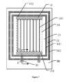
- FIG. 7 illustrates a schematic top view of another exemplary organic light-emitting display panel consistent with disclosed embodiments of the present disclosure
- FIG. 8 illustrates a schematic DD′-sectional view of another exemplary organic light-emitting display panel in FIG. 7 consistent with disclosed embodiments of the present disclosure
- FIG. 9 illustrates a schematic top view of another exemplary organic light-emitting display panel consistent with disclosed embodiments of the present disclosure.
- FIG. 10 illustrates a schematic EE′-sectional view of another exemplary organic light-emitting display panel in FIG. 9 consistent with disclosed embodiments of the present disclosure
- FIG. 11 illustrates exemplary film layers of an anode of another organic light-emitting display panel in FIG. 3 consistent with disclosed embodiments of the present disclosure
- FIG. 12 illustrates a schematic top view of another exemplary organic light-emitting display panel consistent with disclosed embodiments of the present disclosure
- FIG. 13 illustrates a schematic top view of another exemplary organic light-emitting display panel consistent with disclosed embodiments of the present disclosure
- FIG. 14 illustrates a schematic local cross-sectional view of another exemplary organic light-emitting display panel consistent with disclosed embodiments of the present disclosure
- FIG. 15 illustrates a schematic diagram of an exemplary display device consistent with disclosed embodiments of the present disclosure
- FIG. 16 illustrates a schematic top view of an exemplary organic light-emitting display motherboard consistent with disclosed embodiments of the present disclosure.
- FIG. 17 illustrates a schematic FF′-sectional view of an exemplary organic light-emitting display motherboard in FIG. 16 consistent with disclosed embodiments of the present disclosure.
- film layers in some regions of the organic light-emitting display panel have poor flatness, and the reliability of the organic light-emitting display panel is sustainably low.
- a metal wire is provided in the organic light-emitting display panel for transmitting electrical signal.
- a first insulation layer is provided on a surface of the metal wire for protecting the metal wire.
- a hollow portion is disposed in the first insulation layer. The hollow portion penetrates through the first insulation layer along a thickness direction of the first insulation layer and exposes a portion of an upper surface of the metal wire.
- Metal particles are adhered to the upper surface of the metal wire in the region where the hollow portion is located. The metal particles cause the upper surface of the metal wire in the region where the hollow portion is located to be uneven, thereby resulting in poor flatness of the subsequently fabricated film layers.
- the main material of the metal particles is metal silver.
- the metal material of the metal wire includes any one of titanium (Ti), aluminum (Al), molybdenum (Mo), copper (Cu), iron (Fe), nickel (Ni), and chromium (Cr). Because work function of metal silver is larger than work function of the metal material of the metal wire, in the acid etching solution, the metal material of the metal wire tends to lose electrons and displace the highly oxidized silver ions (Ag + ) in the etching solution. The silver ions (Ag + ) form the metal particles after obtaining the electrons. The metal particles will be adhered to the upper surface of the metal wire in the region where the hollow portion is located, resulting in the poor flatness of the subsequently fabricated film layers and low reliability of the organic light-emitting display panel.
- the material of the metal wire in the organic light-emitting display panel often includes aluminum (Al).
- the silver ions (Ag + ) will form the metal particles after obtaining the electrons, and the metal particles will be adhered to the upper surface of the aluminum metal wire in the region where the hollow portion is located.
- the present disclosure provides an organic light-emitting display panel with improved reliability.
- FIG. 1 illustrates a schematic diagram of an organic light-emitting display panel consistent with disclosed embodiments of the present disclosure.
- the organic light-emitting display panel may include a base substrate 00 , a metal wire 10 disposed on the base substrate 00 , a first insulation layer 20 and a conductive portion 30 .
- the metal wire 10 may have a first surface facing the base substrate 00 and an opposing second surface.
- the opposing second surface of the metal wire 10 may be an upper surface 11 of the metal wire.
- the material of the metal wire 10 may include a first metal.
- the first insulation layer 20 may cover the upper surface 11 of the metal wire 10 .
- the first insulation layer 20 may include at least one hollow portion 21 penetrating through the first insulation layer 20 along a thickness direction of the first insulation layer 20 and exposing a portion of the upper surface 11 of the metal wire.
- the conductive portion 30 may not overlap with the hollow portion 21 along a direction ‘z’ perpendicular to the base substrate 00 .
- the conductive portion 30 may be electrically connected to the metal wire 10 .
- the work function of a material of the conductive portion 30 may be G1, the work function of metal silver may be G2, and the work function of the first metal may be G3, where G1>G2>G3.
- the work function also known as a threshold energy, is defined in solid physics as the minimum energy required to move an electron from the interior of a solid to a surface of the object.
- the work function may refer to the work function of a metal.
- the value of the work function may indicate the strength of the electrons bound in the metal. The larger the work function, the less likely the electrons are intended to leave the metal.
- the work function can be simply understood as the ability of the object to possess or capture the electrons. The lower the work function of a substance, the easier the substance is to be oxidized. The higher the work function of a substance, the less likely the substance is to be oxidized.
- the disclosed display panel may be an organic light-emitting display panel, which may include a plurality of organic light-emitting diodes (OLEDs) (not illustrated in FIG. 1 ).
- OLEDs organic light-emitting diodes
- the base substrate 00 may be a rigid substrate.
- the base substrate 00 may be made of a glass material.
- the base substrate 00 may be a flexible substrate.
- the base substrate 00 may be made of a resin material. The material of the base substrate 00 is not limited by the present disclosure and may be determined according to various application scenarios.
- the metal wire 10 may be disposed on the base substrate 00 . Any appropriate films may be disposed between the metal wire 10 and the base substrate 00 , which are not limited by the present disclosure.
- the metal wire 10 may be made of a metal material having desired electrical conductivity.
- the metal wire 10 may be configured to transmit an electrical signal.
- the material of the metal wire 10 may include one type of metal, a combination of two or more types of metals, or two or more types of metal alloys, etc.
- the specific metal material of the metal wire 10 and the function of the electrical signal transmitted by the metal wire 10 are not limited by the present disclosure and may be determined according to various application scenarios.
- the first insulation layer 20 may cover the upper surface 11 of the metal wire.
- the first insulation layer 20 may have an insulating function and may prevent the metal wire 10 from electrical leakage.
- the first insulation layer 20 may protect the metal wire 10 from being damaged in subsequent processes for fabricating the organic light-emitting display panel.
- the first insulation layer 20 may be made of an organic material, or an inorganic material, which is not limited by the present disclosure and may be determined according to various application scenarios.
- the first insulation layer 20 may include at least one hollow portion 21 penetrating through the first insulation layer 20 along the thickness direction of the first insulation layer 20 and exposing a portion of the upper surface 11 of the metal wire.
- the upper surface 11 of the metal wire in the region where the hollow portion 21 is located may not be protected by the first insulation layer 20 and, thus, may be exposed in the acid etching solution.
- the first metal in the material of the metal wire 10 may easily lose electrons and become first metal cations.
- the organic light-emitting display panel may include a plurality of film layer structures. Portion of the film layer structures may be made of metal silver. When patterning the film layer structures containing metal materials using an acid etching solution, the etching solution may include silver ions.
- the conductive portion 30 which may be electrically connected to the metal wire 10 , may be provided.
- the work function of the material of the conductive portion may be G1
- the work function of the metal silver may be G2
- the work function of the first metal may be G3, where G1>G2>G3.
- the conductive portion 30 may resolve the issue that the silver ions form metal particles on the upper surface of the metal wire in the region where the hollow portion 21 is located. The reasons may be explained as follows.
- the work function of the material of the conductive portion 30 may be configured to be greater than the work function of the first metal.
- the work function also known as a threshold energy, is defined in solid physics as the minimum energy required to move an electron from the interior of a solid to a surface of the object.
- the larger the work function of a material the more difficult it is for the material to lose electrons.
- the smaller the work function of a material the easier it is for the material to lose electrons.
- the work function of the material of the conductive portion may be G1, the work function of the metal silver may be G2, and the work function of the first metal may be G3, where G1>G2>G3. That is, the work function G1 of the material of the conductive portion 30 >the work function G2 of the metal silver>the work function G3 of the first metal.
- the material of the conductive portion 30 may be the most difficult to lose electrons, the metal silver may be difficult to lose electrons, and the first metal may be the easiest to lose electrons.
- Contact effect is an electrical effect caused by the contact of two different materials, in which the generated electrical effect is different from the electrical effect when the two materials are not in touch with each other.
- Contact effect is a fairly widespread class of effects, existing between numerous materials such as metal-metal, metal-semiconductor, metal-electrolyte, and metal-oxide, etc.
- the contact effect is related to the work function.
- the contact effect may exist between the conductive portion 30 and the metal wire 10 . Because the work function of the material of the conductive portion 30 is greater than the work function of the first metal in the metal wire 10 , the first metal in the metal wire 10 may be more likely to lose electrons than the material of the conductive portion 30 , and, thus, the electrons in the metal wire 10 may move toward the conductive portion 30 .
- a potential barrier for the silver ions in the acid etching solution to directly acquire electrons from the metal wire 10 may be substantially large, while a potential barrier for the silver ions to acquire lost electrons of the metal wire 10 through the conductive portion 30 may be substantially small.
- the silver ions may not be easily reduced on the surface of the metal wire 10 to form metal particles adhered to the upper surface 11 of the metal wire in the region where the hollow portion 21 is located.
- the silver ions may tend to be reduced on the surface of the conductive portion 30 to form metal particles which are adhered to the surface of the conductive portion 30 .
- the upper surface 11 of the metal wire may maintain a substantially smooth and flat structure under the protection of the conductive portion 30 . Accordingly, the issues of poor flatness of the subsequently manufactured film layers may be resolved, and the reliability of the organic light-emitting display panel may be improved.
- the material of the conductive portion 30 may be the most difficult to lose electrons, the metal silver may be difficult to lose electrons, and the first metal may be the easiest to lose electrons. In other words, the material of the conductive portion 30 may be the easiest to acquire electrons.
- the contact effect may exist between the conductive portion 30 and the object containing metal silver. Electrons of silver may move toward the conductive portion 30 , and silver may turn into silver ions. Therefore, when the material of the conductive portion 30 and the silver ions coexist, the material of the conductive portion 30 may preferentially acquire electrons.
- the conductive portion 30 may be easier to acquire electrons than the silver ions. Therefore, the conductive portion 30 may be easier to be reduced, while the silver ions in the etching solution may not be easy to be reduced.
- the silver ions may not be easy to acquire electrons to form metal particles adhered to the upper surface 11 of the metal wire in the region where the hollow portion 21 is located. Therefore, the upper surface 11 of the metal wire may maintain a substantially smooth and flat structure under the protection of the conductive portion 30 . Accordingly, the issues of poor flatness of the subsequently manufactured film layers may be resolved, and the reliability of the organic light-emitting display panel may be improved.
- the conductive portion 30 may not overlap with the hollow portion 21 along the direction ‘z’ perpendicular to the base substrate 00 . That is, the conductive portion 30 may be disposed in a region other than the hollow portion 21 , without damaging the hollow structure of the first insulation layer 20 and without affecting the structural design requirements of the organic light-emitting display panel.
- FIG. 2 illustrates a schematic local cross-sectional view of another exemplary organic light-emitting display panel consistent with disclosed embodiments of the present disclosure.
- the similarities between FIG. 1 and FIG. 2 are not repeated herein, while certain differences may be explained.
- the base substrate 00 may be a flexible substrate.
- the base substrate 00 may be made of polyimide (PI).
- the organic light-emitting display panel may also include a thin film encapsulation layer 40 .
- the thin film encapsulation layer 40 may cover the upper surface 11 of the metal wire in the region where the hollow portion 21 is located.
- the thin film encapsulation layer 40 may prevent outside moisture, oxygen and impurities from entering the display panel, and protect the film layer structures inside the organic light-emitting display panel.
- the organic light-emitting diode may be fabricated by a vapor deposition manufacturing process.
- the fabricated film layer structures may be loose, and the material of the organic light-emitting diode may be easily eroded by moisture, oxygen and impurities in the air.
- the thin film encapsulation layer 40 may be able to protect the organic light-emitting diode.
- the thin film encapsulation layer 40 may include one, two or three or more film layers. In one embodiment, the thin film encapsulation layer 40 may include organic layers and inorganic layers that are alternatively arranged.
- the base substrate 00 may be a flexible substrate having a bendable property. In one embodiment, the thin film encapsulation layer 40 may also have desired bendability. For example, the organic light-emitting display panel may be rollable, bendable and foldable.
- the specific material and film layer structures of the thin film encapsulation layer 40 are not limited by the present disclosure and may be determined according to various application scenarios.
- the upper surface 11 of the metal wire in the region where the hollow portion 21 is located may be covered with the thin film encapsulation layer 40 .
- the encapsulation performance of the thin film encapsulation layer 40 may be affected, resulting in encapsulation failure of the thin film encapsulation layer 40 . Therefore, the yield of the organic light-emitting display panel may be affected.
- metal particles may not be easily formed to be adhered to the upper surface 11 of the metal wire in the region where the hollow portion 21 is located.
- the upper surface 11 of the metal wire may maintain a substantially smooth and flat structure under the protection of the conductive portion 30 without affecting the encapsulation performance of the thin film encapsulation layer 40 . Therefore, the reliability of the organic light-emitting display panel may be enhanced, and the yield of the organic light-emitting display panel may be improved.
- FIG. 3 illustrates a schematic local cross-sectional view of another exemplary organic light-emitting display panel consistent with disclosed embodiments of the present disclosure.
- the similarities between FIG. 2 and FIG. 3 are not repeated herein, while certain differences may be explained.
- the organic light-emitting display panel may also include a thin film transistor layer 50 and an organic light-emitting diode layer 51 that are sequentially disposed on the base substrate 00 .
- the thin film transistor layer 50 may include a gate metal layer 501 , a semiconductor layer 502 and a source-drain metal layer 503 .
- the thin film transistor layer 50 may include a plurality of thin film transistors ST.
- the thin film transistor ST may include a gate ST 1 , a semiconductor portion ST 2 , a source ST 3 , and a drain ST 4 .
- the gate ST 1 may be located in the gate metal layer 501
- the semiconductor portion ST 2 may be located in the semiconductor layer 502
- the source ST 3 and the drain ST 4 may be disposed in the same layer, and in the source-drain metal layer 503 .
- the organic light-emitting diode layer 51 may include a plurality of organic light-emitting diodes OL.
- the number of the thin film transistors ST is one and the number of the organic light-emitting diodes OL is one, which is for illustrative purposes and is not intended to limit the scope of the present disclosure.
- the number of the thin film transistors ST and the number of the organic light-emitting diodes OL may be any appropriate number, which may be determined according to various application scenarios.
- a top gate transistor (the gate is disposed above the semiconductor portion) is illustrated, which is for illustrative purposes and is not intended to limit the scope of the present disclosure.
- the thin film transistor may have either a top gate structure or a bottom gate structure, which is not limited by the present disclosure and may be determined according to various application scenarios.
- the source-drain metal layer 503 may include the metal wire 10 . That is, the metal wire 10 may be made of a same material and disposed in a same layer as the source ST 3 and the drain ST 4 . In the manufacturing process of the organic light-emitting display panel, the same metal film layer may be etched using a mask to simultaneously form the metal wire 10 , the source ST 3 and the drain ST 4 in the same manufacturing process.
- the material of the metal wire 10 may include the first metal, which may be metal aluminum.
- Metal aluminum has desired electrical conductivity, ductility, and, thus, may be a desired material for fabricating the metal wire 10 .
- the metal wire 10 may include three stacked metal layers.
- the metal wire may include two metal titanium layers and a metal aluminum layer sandwiched between the two metal titanium layers.
- the first insulation layer 20 may be a planarization (PLN) layer, which may be disposed between the thin film transistor layer 50 and the organic light-emitting diode layer 51 .
- the planarization layer may be made of an organic material.
- the planarization layer may have a thick film layer and have a planarization effect.
- the planarization layer may have a first surface facing the base substrate 00 and an opposing second surface.
- the thin film transistor layer 50 may have a non-uniform thickness due to the structure of the thin film transistor layer 50 .
- the planarization layer may cover the thin film transistor layer 50 .
- a distance between the opposing second surface of the planarization layer and the base substrate 00 may be uniform, and the opposing second surface of the planarization layer may be substantially flat, which may provide a desired foundation for the subsequent fabrication of the organic light-emitting diode layer 51 .
- FIG. 4 illustrates a circuit diagram of an exemplary pixel circuit in an exemplary organic light-emitting display panel consistent with disclosed embodiments of the present disclosure.
- the similarities between FIG. 3 and FIG. 4 are not repeated herein, while certain differences may be explained.
- the organic light-emitting display panel may include a plurality of pixels P, and the pixel P may include a pixel circuit PC.
- FIG. 4 illustrates a structure of one pixel P, which is for illustrative purposes, and is not intended to limit the scope of the present disclosure.
- the organic light-emitting display panel may include a plurality of pixels P for implementing the display function of the organic light-emitting display panel, i.e., for displaying images.
- the pixel circuit PC may include an organic light-emitting diode OL, a driving transistor DT, a high-potential signal line PVDD and a low-potential signal line PVEE.
- the high-potential signal line PVDD may be electrically connected to a source of the driving transistor DT.
- a drain of the driving transistor DT may be electrically connected to an anode of the organic light-emitting diode OL.
- the low-potential signal line PVEE may be electrically connected to a cathode of the organic light emitting diode OL.
- the metal wire 10 may be the high-potential signal line PVDD.
- a potential on the high-potential signal line PVDD may be higher than a potential on the low-potential signal line PVEE.
- the high-potential signal line PVDD may provide a high-potential voltage to the driving transistor DT to drive the organic light-emitting diode OL to emit light.
- the pixel circuit PC may compensate a threshold voltage of the driving transistor DT, thereby reducing the non-uniformity display phenomenon caused by the threshold voltage shift of the driving transistor DT.
- the pixel circuit PC may also include a first transistor T 1 and a capacitive element C.
- a drain of the first transistor T 1 may be electrically connected to a first node N 1 .
- a gate of the driving transistor DT may be electrically connected to the first node N 1 .
- a first plate of the capacitive element C may be electrically connected to the first node, and a second plate of the capacitive element C may be electrically connected to the anode of the organic light-emitting diode OL.
- the pixel circuit PC includes two transistors (a driving transistor DT and a first transistor T 1 ), one capacitor C and one light-emitting diode OL, which is for illustrative purposes and is not intended to limit the scope of the present disclosure.
- the structure of the pixel circuit PC is not limited by the present disclosure and may be determined according to various application scenarios in practical applications.
- the pixel circuit may include a plurality of transistors and one or more capacitor.
- the metal wire may be the high-potential signal line PVDD.
- the high-potential signal lines PVDD of the plurality of pixels P may be electrically connected to each other.
- metal particles may be suppressed to be adhered to the surface of the high-potential signal line PVDD in the region where the hollow portion is located may be improved, such that the reliability of the organic light-emitting display panel may be enhanced, and the yield of the organic light-emitting display panel may be increased.
- FIG. 5 illustrates a schematic top view of an exemplary organic light-emitting display panel consistent with disclosed embodiments of the present disclosure
- FIG. 6 illustrates a schematic CC′-sectional view of an exemplary organic light-emitting display panel in FIG. 5 consistent with disclosed embodiments of the present disclosure.
- the similarities between FIG. 3 and FIG. 6 are not repeated herein, while certain differences may be explained.
- the organic light-emitting display panel may include a display region ‘AA’ and a non-display region ‘BB’ surrounding the display region ‘AA’.
- the hollow portion 21 may have an annular shape, and may be located in the non-display region ‘BB’.
- the first insulation layer 20 may be made of an organic material, and the structure may be substantially loose. Outside moisture, oxygen and impurities in the air may enter the interior of the organic light-emitting display panel through the first insulation layer 20 .
- the hollow portion 21 having an annular shape and disposed in the non-display region ‘BB’ may separate the first insulation layer 20 , and, thus, the hollow portion 21 may cut off the transmission path for the outside moisture, oxygen and impurities in the air to enter the display region ‘AA’. Therefore, the outside moisture, oxygen and impurities in the air may be prevented from entering the interior of the organic light-emitting display panel through the first insulation layer 20 , and the reliability of the organic light-emitting display panel may be further enhanced accordingly.
- the non-display region ‘BB’ may include a first barrier spacer ‘BA 1 ’ and a second barrier spacer ‘BA 2 ’.
- the first barrier spacer ‘BA 1 ’ may be disposed around the display region ‘AA’
- the second barrier spacer ‘BA 2 ’ may be disposed around the first barrier spacer ‘BA 1 ’. That is, the first barrier spacer ‘BA 1 ’ may be disposed between the second barrier spacer ‘BA 2 ’ and the display region ‘AA’.
- the second barrier spacer ‘BA 2 ’ may have a first surface facing the base substrate 00 and an opposing second surface
- the second barrier spacer ‘BA 2 ’ may have a first side arranged close to the display region ‘AA’ and an opposing second side far away from the display region ‘AA’.
- the thin film encapsulation layer 40 may cover the display region ‘AA’ and extend to a region between the first barrier spacer ‘BA 1 ’ and the second barrier spacer ‘BA 2 ’. In another embodiment, the thin film encapsulation layer 40 may cover the display region ‘AA’ and extend to the opposing second surface of the second barrier spacer ‘BA 2 ’. In another embodiment, the thin film encapsulation layer 40 may cover the display region ‘AA’ and extend to a region at the opposing second side of the second barrier spacer ‘BA 2 ’. The metal wire 10 may extend from the display region ‘AA’ to the region at the second opposing side of the second barrier spacer ‘BA 2 ’.
- the first barrier spacer ‘BA 1 ’ and the second barrier spacer ‘BA 2 ’ may be disposed in the non-display region ‘BB’.
- the first barrier spacer ‘BA 1 ’ and the second barrier spacer ‘BA 2 ’ may have a dam structure, and a cross-section of the dam structure may have a trapezoid shape.
- the first insulation layer 20 may have a first surface facing the base substrate 00 and an opposing second surface.
- the first barrier spacer ‘BA 1 ’ and the second barrier spacer ‘BA 2 ’ may be disposed on the opposing second surface of the first insulation layer 20 and extend along a thickness direction of the organic light-emitting display panel.
- the first barrier spacer ‘BA 1 ’ and the second barrier spacer ‘BA 2 ’ may include a portion of the first insulation layer 20 .
- Both the first barrier spacer ‘BA 1 ’ and the second barrier spacer ‘BA 2 ’ may be disposed around the display region ‘AA’, and may prevent outside moisture, oxygen and impurities in the air from entering the display panel.
- the thin film encapsulation layer 40 may cover the display region ‘AA’ and extend to the region between the first barrier spacer ‘BA 1 ’ and the second barrier spacer ‘BA 2 ’.
- the thin film encapsulation layer 40 may cover the display region ‘AA’ and extend to the opposing second surface of the second barrier spacer ‘BA 2 ’.
- the thin film encapsulation layer 40 may cover the display region ‘AA’ and extend to the region at the opposing second side of the second barrier spacer ‘BA 2 ’.
- the thin film encapsulation layer 40 may form an undulating structure in the non-display region ‘BB’ under the influence of the structures of the first barrier spacer ‘BA 1 ’ and the second barrier spacer ‘BA 2 ’. Accordingly, the outside moisture, oxygen and impurities in the air may be prevent from entering the display region ‘AA’, and, thus, the organic light-emitting diode OL may be protected from being eroded.
- the metal wire 10 when the metal wire 10 is the high-potential signal line PVDD (i.e., when the metal wire transmits a high-potential signal), the metal wire 10 may supply a high-potential voltage to a plurality of pixels in the display region.
- the metal wire 10 may include a first main wire 101 , a second main wire 102 , and a plurality of wire traces 103 .
- the first main wire 101 and the second main wire 102 may be disposed on two opposing sides of the display region ‘AA’, i.e., the two side are opposing to each other.
- the plurality of wire traces 103 may be disposed in the display region ‘AA’.
- the plurality of wire traces 103 may be electrically connected to the first main wire 101 and the second main wire 102 in the non-display region ‘BB’, respectively.
- the hollow portion may be disposed in any appropriate positions of the organic light-emitting display panel, and certain exemplary positions of the hollow portion will be explained in the following, which are for illustrative purposes and are not intended to limit the scope of the present disclosure.
- FIG. 5 illustrates a schematic top view of an exemplary organic light-emitting display panel consistent with disclosed embodiments of the present disclosure
- FIG. 6 illustrates a schematic CC′-sectional view of an exemplary organic light-emitting display panel in FIG. 5 consistent with disclosed embodiments of the present disclosure.
- the hollow portion 21 may be located in the region between the first barrier spacer ‘BA 1 ’ and the second barrier spacer ‘BA 2 ’.
- the hollow portion 21 , the first barrier spacer ‘BA 1 ’, the second barrier spacer ‘BA 2 ’ and the thin film encapsulation layer 40 may cooperate to prevent outside moisture, oxygen and impurities in the air from entering the interior of the organic light-emitting display panel through the first insulation layer 20 . Therefore, the reliability of the organic light-emitting display panel may be further enhanced.
- FIG. 7 illustrates a schematic top view of another exemplary organic light-emitting display panel consistent with disclosed embodiments of the present disclosure
- FIG. 8 illustrates a schematic DD′-sectional view of another exemplary organic light-emitting display panel in FIG. 7 consistent with disclosed embodiments of the present disclosure.
- FIG. 7 follows the reference numerals in FIG. 5
- FIG. 8 follows the reference numerals in FIG. 6 , and the same or similar features are not repeated herein.
- the hollow portion 21 may be located in the region between the first barrier spacer ‘BA 1 ’ and the second barrier spacer ‘BA 2 ’ and, meanwhile, the hollow portion 21 may be located in a region between the first barrier spacer ‘BA 1 ’ and the display region ‘AA’.
- the hollow portion 21 , the first barrier spacer ‘BA 1 ’, the second barrier spacer ‘BA 2 ’ and the thin film encapsulation layer 40 may cooperate to prevent outside moisture, oxygen and impurities in the air from entering the interior of the organic light-emitting display panel through the first insulation layer 20 . Therefore, the reliability of the organic light-emitting display panel may be further enhanced.
- FIG. 9 illustrates a schematic top view of another exemplary organic light-emitting display panel consistent with disclosed embodiments of the present disclosure
- FIG. 10 illustrates a schematic EE′-sectional view of another exemplary organic light-emitting display panel in FIG. 9 consistent with disclosed embodiments of the present disclosure.
- FIG. 9 follows the reference numerals in FIG. 7
- FIG. 10 follows the reference numerals in FIG. 8 , and the same or similar features are not repeated herein.
- the hollow portion 21 may also be located in the region at the opposing second side of the second barrier spacer ‘BA 2 ’.
- the opposing second side of the second barrier spacer ‘BA 2 ’ is the side far away from the display region AA.
- the hollow portion 21 , the first barrier spacer ‘BA 1 ’, the second barrier spacer ‘BA 2 ’ and the thin film encapsulation layer 40 may cooperate to prevent outside moisture, oxygen and impurities in the air from entering the interior of the organic light-emitting display panel through the first insulation layer 20 . Therefore, the reliability of the organic light-emitting display panel may be further enhanced.
- the hollow portion 21 may be disposed in any one of the region between the first barrier spacer ‘BA 1 ’ and the second barrier spacer ‘BA 2 ’, the region between the first barrier spacer ‘BA 1 ’ and the display region ‘AA’, and the region at the opposing second side of the second barrier spacer ‘BA 2 ’. In another embodiment, the hollow portion 21 may be simultaneously disposed in any two of the region between the first barrier spacer ‘BA 1 ’ and the second barrier spacer ‘BA 2 ’, the region between the first barrier spacer ‘BA 1 ’ and the display region ‘AA’, and the region at the opposing second side of the second barrier spacer ‘BA 2 ’.
- the hollow portion 21 may be disposed in all of the region between the first barrier spacer ‘BA 1 ’ and the second barrier spacer ‘BA 2 ’, the region between the first barrier spacer ‘BA 1 ’ and the display region ‘AA’, and the region at the opposing second side of the second barrier spacer ‘BA 2 ’. That is, the hollow portion 21 may be disposed in at least one of the region between the first barrier spacer ‘BA 1 ’ and the second barrier spacer ‘BA 2 ’, the region between the first barrier spacer ‘BA 1 ’ and the display region ‘AA’, and the region at the opposing second side of the second barrier spacer ‘BA 2 ’.
- the material of the conductive portion 30 may include a conductive metal oxide having a substantially strong oxidation.
- the conductive metal oxide may preferentially obtain electrons and undergo a reduction reaction with respect to the silver ions. Therefore, the silver ions in the etching solution may be prevented from undergoing a reduction reaction to form the metal particles and, accordingly, the metal particles may be suppressed to be adhered to the upper surface 11 of the metal wire in the region where the hollow portion 21 is located.
- the conductive portion 30 may be made of at least one of indium oxide (In 2 O 3 ), zinc oxide (ZnO), tin oxide (SnO 2 ), and gallium oxide (Ga 2 O 3 ).
- Indium oxide, zinc oxide, tin oxide, and gallium oxide may have substantially strong oxidation.
- one selected or a combination of two selected from indium oxide, zinc oxide, tin oxide, and gallium oxide are often used as conductive materials in the organic light-emitting display panel, and may be used for fabricating electrodes.
- the conductive portion By fabricating the conductive portion by using at least one of indium oxide, zinc oxide, tin oxide and gallium oxide, additional raw materials may not be introduced for manufacturing the organic light-emitting display panel, and new processes may not be developed for fabricating the conductive portion. Therefore, the cost of the organic light-emitting display panel may be reduced, and the production efficiency may be improved.
- the organic light-emitting diode layer 51 may include a plurality of organic light-emitting diodes OL.
- the organic light-emitting diode OL may include an anode OL 1 , a cathode OL 2 , and an organic light-emitting portion OL 3 disposed between the anode OL 1 and the cathode OL 2 .
- different colors of light may be emitted by configuring the materials of the organic light-emitting portion OL 3 .
- the anode OL 1 may include a first sub-layer OL 11 , a second sub-layer OL 12 and a third sub-layer OL 13 stacked together.
- the materials of the first sub-layer OL 11 and the third sub-layer OL 13 may include indium tin oxide (ITO), also known as a tin-doped indium oxide, or a mixture of indium oxide (In 2 O 3 ) and tin oxide (SnO 2 ).
- ITO indium tin oxide
- the indium tin oxide may have desired electrical conductivity and may be transparent in a thin film form.
- the material of the second sub-layer OL 12 may include silver.
- the second sub-layer OL 12 may have a desired effect of reflecting light.
- Portion of light generated by the organic light-emitting portion OL 3 may be emitted from the cathode OL 2 under the reflection of the second sub-layer OL 12 , and the organic light-emitting display panel may have a top-emission structure.
- the etching solution may include silver ions (Ag + ).
- the material of the metal wire 10 may include aluminum (Al).
- the metal wire 10 may be the high-potential signal line PVDD.
- the non-display region ‘BB’ may include a bonding region ‘BB 1 ’, and the bonding region ‘BB 1 ’ may include a plurality of conductive welding pads 15 .
- the bonding region ‘BB 1 ’ may be bonded with an integrated circuit (IC), or a flexible printed circuit (FPC), etc.
- the metal wire 10 may extend to the bonding region ‘BB 1 ’ of the organic light-emitting display panel.
- the bonding region ‘BB 1 ’ may be located in the non-display region ‘BB’ of the display panel.
- the metal wire 10 may obtain external electrical signals of the display panel through the IC or the flexible circuit board bonded to the bonding region ‘BB 1 ’.
- the metal wire 10 in a lower border region may extend to other film layers by a wire-changing method thereby avoiding the exposure of the upper surface 11 of the metal wire through the hollow portion 21 in the first insulation layer 20 .
- the design of the wire-changing method may be substantially difficult.
- a plurality of signal lines, and circuit elements may be disposed in the non-display region ‘BB’.
- BB non-display region
- a side of the non-display region ‘BB’ where the bonding region is located is often referred to the lower border region, and the plurality of signal lines, and circuit elements, such as demux circuit, etc., may be disposed in the lower border region.
- the metal wire 10 in the lower border region When the metal wire 10 in the lower border region extends to other conductive layers by the wire-changing method, the metal wire 10 may intersect the signal lines and circuit elements in the lower border region, causing a short circuit.
- the structure of the originally complicated lower border region may become more complicated, and the design difficulty of the organic light-emitting display panel may be increased. Therefore, the metal wire 10 in the lower border region may not be desired to extend to other conductive layers by the wire-changing method.
- the issue that the hollow portion 21 in the first insulation layer 20 exposes the upper surface 11 of the metal wire may not be resolved by the wire-changing method.
- the conductive portion 30 may be provided, thereby resolving the issue that the metal particles are adhered to the upper surface 11 of the metal wire in the region where the hollow portion 21 is located.
- the conductive portion 30 and the anode OL 1 may be made of a same material.
- the anode OL 1 and the conductive portion 30 may be simultaneously formed in a same process without introducing any additional process for manufacturing the conductive portion 30 .
- the etching solution may include silver ions (Ag + ).
- the material of the metal wire 10 may include aluminum (Al).
- Aluminum (Al) may easily lose electrons in an acid etching solution, and the chemical reaction formula is shown in the following: Al ⁇ Al 3+ +3 e ⁇ (Formula 1).
- the metal wire 10 may be electrically connected to the conductive portion 30 , and the work function of the material of the conductive portion 30 may be greater than the work function of the first metal.
- the silver ions may easily undergo a reduction reaction on the surface of the conductive portion 30 to form metal particles, which are adhered to the surface of the conductive portion 30 .
- the chemical reaction formula for silver ions (Ag + ) obtaining electrons is shown in the following: Ag + +e ⁇ ⁇ Ag (Formula 2).
- indium oxide (In 2 O 3 ) may be easier to obtain electrons than silver ions (Ag + ), and silver ions may be difficult to obtain electrons.
- Portion of the indium oxide (In 2 O 3 ) may undergo a reduction reaction, and the chemical reaction formula for indium oxide (In 2 O 3 ) obtaining electrons is shown in the following: In 2 O 3 +6 e ⁇ ⁇ 2In+3O 2 (Formula 3).
- the phenomenon that the silver ions undergo a reduction reaction to form the metal particles, which are adhered to the upper surface 11 of the metal wire in the region where the hollow portion 21 is located, may be suppressed.
- the upper surface 11 of the metal wire may maintain a substantially smooth and flat structure under the protection of the conductive portion 30 . Accordingly, the issues of poor flatness of the subsequently manufactured film layers and low reliability of the organic light-emitting display panel may be resolved, and the reliability of the organic light-emitting display panel may be improved.
- FIG. 12 illustrates a schematic top view of another exemplary organic light-emitting display panel consistent with disclosed embodiments of the present disclosure.
- the conductive portion 30 may be disposed in the non-display region ‘BB’, and may not occupy the space of the display region ‘AA’. Therefore, the conductive portion 30 may be prevented from affecting the display effect of the display region ‘AA’.
- the conductive portion 30 may have a strip shape extended along a first direction ‘x’.
- the conductive portion 30 may be disposed in a side of the display region ‘AA’, and the side of the display region ‘AA’ may be close to the bonding region ‘BB 1 ’.
- the conductive portion 30 may overlap with the first main wire 101 .
- the conductive portion 30 may be formed into a strip shape with a large area, facilitating the conductive portion 30 to sufficiently undergo a reduction reaction. Therefore, the phenomenon that the silver ions in the etching solution undergo a reduction reaction to form the metal particles, which are adhered to the upper surface 11 of the metal wire in the region where the hollow portion 21 is located, may be suppressed, and the reliability of the organic light-emitting display panel may be enhanced.
- a shape of the organic light-emitting display panel is rectangular, which is for illustrative purposes and is not intended to limit the scope of the present disclosure.
- the shape of the organic light-emitting display panel is a circular, or an oval, etc.
- the shape and extending direction of the conductive portion 30 may be adaptively adjusted, which are not limited by the present disclosure.
- FIG. 13 illustrates a schematic top view of another exemplary organic light-emitting display panel consistent with disclosed embodiments of the present disclosure.
- the conductive portion 30 may include a plurality of sub-conductive portions 301 .
- a sub-conductive portion 301 may overlap with the metal wire 10 in the direction perpendicular to the base substrate 00 .
- the sub-conductive portion 301 may overlap with the first main wire 101 .
- the sub-conductive portion 301 may overlap with the second main wire 102 .
- the conductive portion 30 may include the plurality of sub-conductive portions 301 .
- Each sub-conductive portion 301 may be physically independent of each other, and may be electrically connected to the metal wire 10 .
- the exposed film edge of the conductive portion 30 in the etching solution may increase.
- the contact area between the conductive portion 30 and silver ions may increase, thereby facilitating the silver ions to obtain the electrons lost by the metal wire 10 through the conductive portion 30 , and facilitating the silver ions to form metal particles on the surface of the conductive portion 30 .
- the conductive portion 30 may promptly and sufficiently undergo a reduction reaction in the etching solution.
- the phenomenon that the silver ions in the etching solution undergo a reduction reaction to form the metal particles, which are adhered to the upper surface 11 of the metal wire in the region where the hollow portion 21 is located, may be suppressed, and the reliability of the organic light-emitting display panel may be enhanced.
- a shape of the sub-conductive portion 301 is a rectangle, which is for illustrative purposes and is not intended to limit the scope of the present disclosure.
- the shape and number of the sub-conductive portions 301 are not limited by the present disclosure and may be determined according to various application scenarios.
- FIG. 14 illustrates a schematic local cross-sectional view of another exemplary organic light-emitting display panel consistent with disclosed embodiments of the present disclosure.
- the similarities between FIG. 10 and FIG. 14 are not repeated herein, while certain differences may be explained.
- the organic light-emitting diode layer 51 may also include a pixel defining layer 41 .
- the conductive portion may have a first surface facing the base substrate 00 and an opposing second surface.
- the pixel defining layer 41 may cover the opposing second surface of the conductive portion 30 .
- the pixel defining layer 41 may include an opening region, and at least a portion of the organic light-emitting diode OL may be disposed in the opening region.
- the pixel defining layer 41 covering the opposing second surface of the conductive portion 30 may protect the conductive portion 30 from being etched or damaged during the subsequent manufacturing process of the organic light-emitting display panel.
- the conductive portion 30 may be disposed on the opposing second surface of the first insulation layer 20 .
- the first insulation layer 20 may include a first through-hole 201 .
- the conductive portion 30 may be electrically connected to the metal wire 10 through the first through-hole 201 .
- the present disclosure also provides a display device.
- the display device may include any one of the disclosed organic light-emitting display panels.
- FIG. 15 illustrates a schematic diagram of an exemplary display device consistent with disclosed embodiments of the present disclosure.
- the display device 100 may include any one of the disclosed organic light-emitting display panels 100 a .
- FIG. 15 illustrates the display device 100 using a mobile phone, which is for illustrative purposes and is not intended to limit the scope of the present disclosure.
- the disclosed display device may be any other display device with a display function, such as a computer, a television, a car display device, etc., and is not limited by the present disclosure.
- the disclosed display device may have the features of the disclosed organic light-emitting display panel. Details may be referred to the corresponding description of the disclosed organic light-emitting display panel, and are not repeated herein.
- the present disclosure also provides an organic light-emitting display motherboard.
- FIG. 16 illustrates a schematic top view of an exemplary organic light-emitting display motherboard consistent with disclosed embodiments of the present disclosure
- FIG. 17 illustrates a schematic FF′-sectional view of an exemplary organic light-emitting display motherboard in FIG. 16 consistent with disclosed embodiments of the present disclosure
- the organic light-emitting display motherboard may include a mother base substrate 200 , a metal wire 10 disposed on the mother base substrate 200 , a first insulation layer 20 and a conductive portion 30 .
- the metal wire 10 may have a first surface facing the mother base substrate 200 and an opposing second surface.
- the opposing second surface of the metal wire 10 may be an upper surface 11 of the metal wire.
- the material of the metal wire 10 may include a first metal.
- the first insulation layer 20 may cover the upper surface 11 of the metal wire.
- the first insulation layer 20 may include at least one hollow portion 21 , and the at least one hollow portion 21 may penetrate through the first insulation layer 20 along a thickness direction of the first insulation layer 20 , and expose a portion of the upper surface 11 of the metal wire 10 .
- the conductive portion 30 may not overlap with the hollow portion 21 along a direction perpendicular to the mother base substrate 200 .
- the conductive portion 30 may be electrically connected to the metal wire 10 .
- the work function of a material of the conductive portion 30 may be G1, the work function of metal silver may be G2, and the work function of the first metal may be G3, where G1>G2>G3.
- the organic light-emitting display motherboard may include a plurality of sub-display panel regions 100 A, and the conductive portion 30 may be disposed in a region other than the sub-display panel regions 100 A.
- the disclosed organic light-emitting display motherboard may include the plurality of sub-display panel regions 100 A. After the organic light-emitting display motherboard is manufactured, a plurality of organic light-emitting display panels may be obtained by cutting the regions other than the sub-display panel regions 100 A through a cutting process.
- one organic light-emitting display motherboard includes four sub-display panel regions 100 A for, which is for illustrative purposes and is not intended to limit the scope of the present disclosure. After the organic light-emitting display motherboard is manufactured, four organic light-emitting display panels may be obtained through a cutting process. In an actual production application, one organic light-emitting display motherboard may include five or more sub-display panel regions 100 A, which is not limited by the present disclosure and may be determined according to various application scenarios.
- the mother base substrate 200 may be a hard substrate.
- the mother base substrate 200 may be made of a glass material.
- the mother base substrate 200 may be a flexible substrate.
- the mother base substrate 200 may be made of a resin material.
- the material of the mother base substrate 200 is not limited by the present disclosure and may be determined according to various application scenarios.
- the metal wire 10 may be disposed on the mother base substrate 200 . Any appropriate films may be disposed between the metal wire 10 and the mother base substrate 200 , which are not limited by the present disclosure.
- the material of the metal wire 10 may include a meta having desired electrical conductivity.
- the metal wire 10 may be configured to transmit an electrical signal.
- the material of the metal wire 10 may include one type of metal, or two or more types of metal, etc.
- the specific metal material of the metal wire 10 and the function of the electrical signal transmitted by the metal wire 10 are not limited by the present disclosure and may be determined according to various application scenarios.
- the first insulation layer 20 may cover the upper surface 11 of the metal wire.
- the first insulation layer 20 may have an insulating function and may prevent the metal wire 10 from electrical leakage.
- the first insulation layer 20 may protect the metal wire 10 from being damaged in subsequent manufacturing process of the organic light-emitting display panel.
- the first insulation layer 20 may be made of an organic material or an inorganic material, which is not limited by the present disclosure and may be determined according to various application scenarios.
- the first insulation layer 20 may include at least one hollow portion 21 penetrating through the first insulation layer 20 along the thickness direction of the first insulation layer 20 and exposing a portion of the upper surface 11 of the metal wire.
- the upper surface 11 of the metal wire in the region where the hollow portion 21 is located may not be protected by the first insulation layer 20 and, thus, may be exposed in the acid etching solution.
- the first metal in the material of the metal wire 10 may easily lose electrons and become the first metal cations.
- the organic light-emitting display motherboard may include a plurality of film layer structures. Portion of the material of the film layer structures may include metal silver. When patterning the film layer structures containing a metal material using an acid etching solution, the etching solution may include silver ions.
- the conductive portion 30 which is electrically connected to the metal wire 10 , may be provided.
- the reasons why the conductive portion 30 may be able to resolve the issue that the silver ions form metal particles on the upper surface 11 of the metal wire in the region where the hollow portion 21 is located may be referred to the foregoing description in the disclosed embodiments, and are not repeated herein.
- the conductive portion 30 may be provided and, thus, the upper surface 11 of the metal wire may maintain a substantially smooth and flat structure under the protection of the conductive portion 30 . Accordingly, the issues of poor flatness of the subsequently manufactured film layers may be resolved, and the reliability of the organic light-emitting display panel may be improved.
- the conductive portion 30 may not overlap with the hollow portion 21 along a direction ‘z’ perpendicular to the mother base substrate 200 . That is, the conductive portion 30 may be disposed in a region other than the hollow portion 21 , without damaging the hollow structure of the first insulation layer 20 and without affecting the structural design requirements of the organic light-emitting display motherboard.
- the sub-display panel region 100 A may include a display region ‘AA’ and a non-display region ‘BB’.
- the hollow portion 21 may have an annular shape and may be disposed in the non-display region ‘BB’.
- the non-display region ‘BB’ may include a first barrier spacer ‘BA 1 ’ and a second barrier spacer ‘BA 2 ’.
- the first barrier spacer ‘BA 1 ’ may be disposed around the display region ‘AA’
- the second barrier spacer ‘BA 2 ’ may be disposed around the first barrier spacer ‘BA 1 ’.
- the metal wire 10 may be a high-potential signal line PVDD, and the metal wire 10 may supply a high-potential voltage to a plurality of pixels in the display region.
- the metal wire 10 may include a first main wire 101 , a second main wire 102 , and a plurality of wire traces 103 .
- the first main wire 101 and the second main wire 102 may be disposed on two sides of the display region ‘AA’ opposing to each other.
- the plurality of wire traces 103 may be disposed in the display region ‘AA’.
- the plurality of wire traces 103 may be electrically connected to the first main wire 101 and the second main wire 102 in the non-display region ‘BB’.
- the hollow portion 21 may be disposed in a region between the first barrier spacer ‘BA 1 ’ and the display region ‘AA’.
- the conductive portion 30 may be disposed in a region other than the sub-display panel regions 100 A. In the cutting process, the conductive portion 30 may be cut away.
- the organic light-emitting display panel obtained by cutting may not include the conductive portion 30 , and the structural design of the organic light-emitting display panel may not be affected.
- the conductive portion 30 may include a plurality of sub-conductive portions 301 .
- the sub-conductive portions 301 may overlap with the metal wire 10 in the direction perpendicular to the mother base substrate 200 .
- the exposed film edge of the conductive portion 30 in the etching solution may increase by providing the plurality of sub-conductive portions 301 .
- the contact area between the conductive portion 30 and silver ions may increase, facilitating the silver ions to obtain the electrons lost by the metal wire 10 through the conductive portion 30 , and facilitating the silver ions to form metal particles on the surface of the conductive portion 30 .
- the conductive portion 30 may promptly and sufficiently undergo a reduction reaction in the etching solution.
- the phenomenon that the silver ions in the etching solution undergo a reduction reaction to form the metal particles, which are adhered to the upper surface 11 of the metal wire in the region where the hollow portion 21 is located, may be resolved, and the reliability of the organic light-emitting display motherboard may be improved.
- the first insulation layer may cover the upper surface of the metal wire.
- the first insulation layer may include at least one hollow portion penetrating through the first insulation layer along the thickness direction of the first insulation layer and exposing portion of the upper surface of the metal wire.
- the conductive portion which is electrically connected to the metal wire, may be provided.
- the work function of the material of the conductive portion may be larger than the work function of metal silver, such that the silver ions in the etching solution may be difficult to undergo a reduction reaction to form the metal particles, which are adhered to the upper surface of the metal wire in the region where the hollow portion is located. Because the work function of the conductive portion is larger than the work function of the material of the metal wire, the silver ions may easily undergo a reduction reaction on the surface of the conductive portion to form metal particles, which are adhered to the surface of the conductive portion. Therefore, the upper surface of the metal wire may maintain a substantially smooth and flat structure, thereby avoiding the precipitation of the metal particles.
- the reliability of the organic light-emitting display panel may be improved, the process yield of the organic light-emitting display panel may be greatly improved, and the production cost may be reduced, facilitating to promote large-scale production and industrial applications of the organic light-emitting display panel.
Landscapes
- Engineering & Computer Science (AREA)
- Microelectronics & Electronic Packaging (AREA)
- Physics & Mathematics (AREA)
- Optics & Photonics (AREA)
- Electroluminescent Light Sources (AREA)
Abstract
Description
Al→Al3++3e − (Formula 1).
Ag+ +e −→Ag (Formula 2).
In2O3+6e −→2In+3O2 (Formula 3).
Claims (20)
Applications Claiming Priority (3)
| Application Number | Priority Date | Filing Date | Title |
|---|---|---|---|
| CN201810000653.8A CN108336109B (en) | 2018-01-02 | 2018-01-02 | Organic light emitting display panel, display device and organic light emitting display motherboard |
| CN201810000653.8 | 2018-01-02 | ||
| CN201810000653 | 2018-01-02 |
Publications (2)
| Publication Number | Publication Date |
|---|---|
| US20180190742A1 US20180190742A1 (en) | 2018-07-05 |
| US10347701B2 true US10347701B2 (en) | 2019-07-09 |
Family
ID=62712106
Family Applications (1)
| Application Number | Title | Priority Date | Filing Date |
|---|---|---|---|
| US15/907,842 Active US10347701B2 (en) | 2018-01-02 | 2018-02-28 | Organic light-emitting display panel, display device and organic light-emitting display motherboard thereof |
Country Status (2)
| Country | Link |
|---|---|
| US (1) | US10347701B2 (en) |
| CN (1) | CN108336109B (en) |
Families Citing this family (27)
| Publication number | Priority date | Publication date | Assignee | Title |
|---|---|---|---|---|
| KR101974086B1 (en) * | 2016-09-30 | 2019-05-02 | 삼성디스플레이 주식회사 | Display module |
| CN109326634B (en) | 2018-09-30 | 2020-11-06 | 云谷(固安)科技有限公司 | Display panel, method for producing the same, and display device |
| CN109713017B (en) | 2019-01-14 | 2021-01-22 | 京东方科技集团股份有限公司 | Display substrate, preparation method thereof and display device |
| US20220100296A1 (en) * | 2019-01-25 | 2022-03-31 | Shenzhen Royole Technologies Co., Ltd. | Flexible touch sensor electrode and manufacturing method therefor |
| CN109904343B (en) * | 2019-02-27 | 2021-10-26 | 昆山国显光电有限公司 | Display device and preparation method thereof |
| CN110071165B (en) * | 2019-05-14 | 2022-05-13 | 京东方科技集团股份有限公司 | Array substrate, manufacturing method thereof and display panel |
| CN110265572A (en) * | 2019-06-12 | 2019-09-20 | 武汉华星光电半导体显示技术有限公司 | Display panel and display module |
| CN110600511A (en) * | 2019-08-26 | 2019-12-20 | 武汉华星光电半导体显示技术有限公司 | Organic light-emitting display panel and preparation method thereof |
| CN112714966B (en) * | 2019-08-27 | 2025-01-10 | 京东方科技集团股份有限公司 | Display substrate and manufacturing method thereof, and display device |
| WO2021035546A1 (en) | 2019-08-27 | 2021-03-04 | 京东方科技集团股份有限公司 | Display substrate and manufacturing method therefor, and display device |
| US12238983B2 (en) | 2019-08-27 | 2025-02-25 | Boe Technology Group Co., Ltd. | Display substrate and manufacturing method thereof, and display device |
| CN110690262A (en) * | 2019-10-16 | 2020-01-14 | 武汉华星光电半导体显示技术有限公司 | Organic light emitting diode display panel and manufacturing method thereof |
| CN110993817B (en) * | 2019-11-26 | 2020-12-25 | 武汉华星光电半导体显示技术有限公司 | OLED display panel |
| CN111584583B (en) * | 2020-05-15 | 2022-07-12 | 武汉华星光电半导体显示技术有限公司 | Display panel and manufacturing method thereof |
| CN111653603B (en) * | 2020-06-18 | 2023-08-29 | 京东方科技集团股份有限公司 | Display substrate and display device |
| US12471424B2 (en) * | 2020-09-07 | 2025-11-11 | Beijing Boe Technology Development Co., Ltd. | Array substrate and manufacturing method therefor, display panel, and backlight module |
| CN112310184A (en) * | 2020-10-30 | 2021-02-02 | 昆山国显光电有限公司 | Display panel and display device |
| CN113013356B (en) * | 2021-02-22 | 2023-02-03 | 京东方科技集团股份有限公司 | Display device, display panel and manufacturing method thereof |
| CN113078170B (en) * | 2021-03-25 | 2024-05-24 | 京东方科技集团股份有限公司 | Display panel and display device |
| CN115552618B (en) * | 2021-04-30 | 2025-03-28 | 京东方科技集团股份有限公司 | Display substrate and display device |
| CN114138136A (en) * | 2021-12-09 | 2022-03-04 | 武汉华星光电半导体显示技术有限公司 | Display panel and display device |
| TWI796079B (en) * | 2022-01-07 | 2023-03-11 | 友達光電股份有限公司 | Device substrate and manufacturing method thereof |
| CN115332306B (en) * | 2022-08-30 | 2025-09-23 | 京东方科技集团股份有限公司 | Display panel and display device |
| CN115802825A (en) * | 2022-11-16 | 2023-03-14 | 深圳市华星光电半导体显示技术有限公司 | Display panel and manufacturing method thereof |
| CN116249388B (en) * | 2023-04-12 | 2025-12-02 | 武汉天马微电子有限公司 | Display panel and display device |
| CN116631320B (en) * | 2023-05-29 | 2026-01-30 | 京东方科技集团股份有限公司 | Display substrate and display device |
| CN118984621B (en) * | 2024-07-31 | 2025-09-12 | 武汉华星光电半导体显示技术有限公司 | Organic light-emitting display panels |
Citations (5)
| Publication number | Priority date | Publication date | Assignee | Title |
|---|---|---|---|---|
| US20060125390A1 (en) * | 2004-12-14 | 2006-06-15 | Sang-Hun Oh | Organic light emitting display with auxiliary electrode line and method of fabricating the same |
| US20070170859A1 (en) * | 2006-01-25 | 2007-07-26 | Dong Soo Choi | Organic light emitting display and method of fabricating the same |
| CN102163613A (en) | 2009-10-22 | 2011-08-24 | 索尼公司 | Display device and method for manufacturing display device |
| US20120112224A1 (en) * | 2009-04-02 | 2012-05-10 | Saint-Gobain Glass France | Method for producing a structure with a textured external surface, intended for an organic light emitting diode device, and a structure with a textured external surface |
| US20180122877A1 (en) * | 2016-10-31 | 2018-05-03 | Lg Display Co., Ltd. | Organic Light Emitting Display Device and Method of Manufacturing the Same |
Family Cites Families (4)
| Publication number | Priority date | Publication date | Assignee | Title |
|---|---|---|---|---|
| JPH05283169A (en) * | 1992-03-31 | 1993-10-29 | Toppan Printing Co Ltd | Organic thin film EL device |
| KR101458402B1 (en) * | 2011-04-01 | 2014-11-06 | 엘지디스플레이 주식회사 | Organic electro-luminescent device |
| KR102455318B1 (en) * | 2015-10-30 | 2022-10-18 | 삼성디스플레이 주식회사 | Organic light emitting display device |
| CN107068720B (en) * | 2017-04-19 | 2019-08-27 | 上海天马微电子有限公司 | Organic light-emitting diode display panel and display device |
-
2018
- 2018-01-02 CN CN201810000653.8A patent/CN108336109B/en active Active
- 2018-02-28 US US15/907,842 patent/US10347701B2/en active Active
Patent Citations (5)
| Publication number | Priority date | Publication date | Assignee | Title |
|---|---|---|---|---|
| US20060125390A1 (en) * | 2004-12-14 | 2006-06-15 | Sang-Hun Oh | Organic light emitting display with auxiliary electrode line and method of fabricating the same |
| US20070170859A1 (en) * | 2006-01-25 | 2007-07-26 | Dong Soo Choi | Organic light emitting display and method of fabricating the same |
| US20120112224A1 (en) * | 2009-04-02 | 2012-05-10 | Saint-Gobain Glass France | Method for producing a structure with a textured external surface, intended for an organic light emitting diode device, and a structure with a textured external surface |
| CN102163613A (en) | 2009-10-22 | 2011-08-24 | 索尼公司 | Display device and method for manufacturing display device |
| US20180122877A1 (en) * | 2016-10-31 | 2018-05-03 | Lg Display Co., Ltd. | Organic Light Emitting Display Device and Method of Manufacturing the Same |
Also Published As
| Publication number | Publication date |
|---|---|
| CN108336109A (en) | 2018-07-27 |
| CN108336109B (en) | 2021-02-02 |
| US20180190742A1 (en) | 2018-07-05 |
Similar Documents
| Publication | Publication Date | Title |
|---|---|---|
| US10347701B2 (en) | Organic light-emitting display panel, display device and organic light-emitting display motherboard thereof | |
| US11737311B2 (en) | Organic light-emitting display apparatus and fabrication method thereof | |
| US10937849B2 (en) | Array substrate and method of manufacturing the same, display panel and display device | |
| KR102814989B1 (en) | Display device | |
| WO2019114204A1 (en) | Organic light-emitting diode apparatus, fabircation method thereof, display panel, and display apparatus | |
| US12185598B2 (en) | Display panel and a display device | |
| US11567604B2 (en) | Display module and display device | |
| KR102807777B1 (en) | Display device and method of manufacturing the same | |
| KR20190052327A (en) | Display device | |
| KR20260008058A (en) | Organic light emitting display device | |
| KR102585982B1 (en) | Organic light emitting display device and method for manufacturing the same | |
| US20250184417A1 (en) | Display apparatus including substrate hole | |
| US11785808B2 (en) | Flexible display device and method of manufacturing the same | |
| KR102832568B1 (en) | A conductive layer and a display panel having the same | |
| CN116056515B (en) | Display panel, display device | |
| JP2021162639A (en) | Active matrix substrate and display device | |
| KR102789541B1 (en) | Organic light emitting display device | |
| CN115955881B (en) | Display panel, display device | |
| KR102935337B1 (en) | Organic light emitting display device | |
| KR102916871B1 (en) | Organic light emitting display device | |
| CN114420727A (en) | Flexible display panel and manufacturing method thereof | |
| KR20250115638A (en) | Flexible display device | |
| CN115954363A (en) | display device | |
| CN117222258A (en) | display screen | |
| CN115955881A (en) | display panel, display device |
Legal Events
| Date | Code | Title | Description |
|---|---|---|---|
| AS | Assignment |
Owner name: XIAMEN TIANMA MICRO-ELECTRONICS CO., LTD., CHINA Free format text: ASSIGNMENT OF ASSIGNORS INTEREST;ASSIGNORS:HE, SHUI;ZHAI, YINGTENG;LIN, YONGXIANG;AND OTHERS;REEL/FRAME:045064/0843 Effective date: 20180224 |
|
| FEPP | Fee payment procedure |
Free format text: ENTITY STATUS SET TO UNDISCOUNTED (ORIGINAL EVENT CODE: BIG.); ENTITY STATUS OF PATENT OWNER: LARGE ENTITY |
|
| STPP | Information on status: patent application and granting procedure in general |
Free format text: RESPONSE TO NON-FINAL OFFICE ACTION ENTERED AND FORWARDED TO EXAMINER |
|
| STPP | Information on status: patent application and granting procedure in general |
Free format text: NOTICE OF ALLOWANCE MAILED -- APPLICATION RECEIVED IN OFFICE OF PUBLICATIONS |
|
| STPP | Information on status: patent application and granting procedure in general |
Free format text: PUBLICATIONS -- ISSUE FEE PAYMENT VERIFIED |
|
| STCF | Information on status: patent grant |
Free format text: PATENTED CASE |
|
| MAFP | Maintenance fee payment |
Free format text: PAYMENT OF MAINTENANCE FEE, 4TH YEAR, LARGE ENTITY (ORIGINAL EVENT CODE: M1551); ENTITY STATUS OF PATENT OWNER: LARGE ENTITY Year of fee payment: 4 |