US10345641B2 - Liquid crystal display apparatus and method of driving liquid crystal display apparatus - Google Patents

Liquid crystal display apparatus and method of driving liquid crystal display apparatus Download PDF

Info

Publication number
US10345641B2
US10345641B2 US15/329,492 US201415329492A US10345641B2 US 10345641 B2 US10345641 B2 US 10345641B2 US 201415329492 A US201415329492 A US 201415329492A US 10345641 B2 US10345641 B2 US 10345641B2
Authority
US
United States
Prior art keywords
liquid crystal
pixel
auxiliary capacitor
electrode
display apparatus
Prior art date
Legal status (The legal status is an assumption and is not a legal conclusion. Google has not performed a legal analysis and makes no representation as to the accuracy of the status listed.)
Expired - Fee Related, expires
Application number
US15/329,492
Other versions
US20170322449A1 (en
Inventor
Kentaro Irie
Masae Kitayama
Current Assignee (The listed assignees may be inaccurate. Google has not performed a legal analysis and makes no representation or warranty as to the accuracy of the list.)
Sakai Display Products Corp
Original Assignee
Sakai Display Products Corp
Priority date (The priority date is an assumption and is not a legal conclusion. Google has not performed a legal analysis and makes no representation as to the accuracy of the date listed.)
Filing date
Publication date
Application filed by Sakai Display Products Corp filed Critical Sakai Display Products Corp
Assigned to SAKAI DISPLAY PRODUCTS CORPORATION reassignment SAKAI DISPLAY PRODUCTS CORPORATION ASSIGNMENT OF ASSIGNORS INTEREST (SEE DOCUMENT FOR DETAILS). Assignors: IRIE, KENTARO, KITAYAMA, MASAE
Publication of US20170322449A1 publication Critical patent/US20170322449A1/en
Application granted granted Critical
Publication of US10345641B2 publication Critical patent/US10345641B2/en
Expired - Fee Related legal-status Critical Current
Adjusted expiration legal-status Critical

Links

Images

Classifications

    • GPHYSICS
    • G09EDUCATION; CRYPTOGRAPHY; DISPLAY; ADVERTISING; SEALS
    • G09GARRANGEMENTS OR CIRCUITS FOR CONTROL OF INDICATING DEVICES USING STATIC MEANS TO PRESENT VARIABLE INFORMATION
    • G09G3/00Control arrangements or circuits, of interest only in connection with visual indicators other than cathode-ray tubes
    • G09G3/03Control arrangements or circuits, of interest only in connection with visual indicators other than cathode-ray tubes specially adapted for displays having non-planar surfaces, e.g. curved displays
    • GPHYSICS
    • G02OPTICS
    • G02FOPTICAL DEVICES OR ARRANGEMENTS FOR THE CONTROL OF LIGHT BY MODIFICATION OF THE OPTICAL PROPERTIES OF THE MEDIA OF THE ELEMENTS INVOLVED THEREIN; NON-LINEAR OPTICS; FREQUENCY-CHANGING OF LIGHT; OPTICAL LOGIC ELEMENTS; OPTICAL ANALOGUE/DIGITAL CONVERTERS
    • G02F1/00Devices or arrangements for the control of the intensity, colour, phase, polarisation or direction of light arriving from an independent light source, e.g. switching, gating or modulating; Non-linear optics
    • G02F1/01Devices or arrangements for the control of the intensity, colour, phase, polarisation or direction of light arriving from an independent light source, e.g. switching, gating or modulating; Non-linear optics for the control of the intensity, phase, polarisation or colour 
    • G02F1/13Devices or arrangements for the control of the intensity, colour, phase, polarisation or direction of light arriving from an independent light source, e.g. switching, gating or modulating; Non-linear optics for the control of the intensity, phase, polarisation or colour  based on liquid crystals, e.g. single liquid crystal display cells
    • G02F1/133Constructional arrangements; Operation of liquid crystal cells; Circuit arrangements
    • G02F1/1333Constructional arrangements; Manufacturing methods
    • G02F1/1335Structural association of cells with optical devices, e.g. polarisers or reflectors
    • G02F1/133509Filters, e.g. light shielding masks
    • G02F1/133514Colour filters
    • GPHYSICS
    • G02OPTICS
    • G02FOPTICAL DEVICES OR ARRANGEMENTS FOR THE CONTROL OF LIGHT BY MODIFICATION OF THE OPTICAL PROPERTIES OF THE MEDIA OF THE ELEMENTS INVOLVED THEREIN; NON-LINEAR OPTICS; FREQUENCY-CHANGING OF LIGHT; OPTICAL LOGIC ELEMENTS; OPTICAL ANALOGUE/DIGITAL CONVERTERS
    • G02F1/00Devices or arrangements for the control of the intensity, colour, phase, polarisation or direction of light arriving from an independent light source, e.g. switching, gating or modulating; Non-linear optics
    • G02F1/01Devices or arrangements for the control of the intensity, colour, phase, polarisation or direction of light arriving from an independent light source, e.g. switching, gating or modulating; Non-linear optics for the control of the intensity, phase, polarisation or colour 
    • G02F1/13Devices or arrangements for the control of the intensity, colour, phase, polarisation or direction of light arriving from an independent light source, e.g. switching, gating or modulating; Non-linear optics for the control of the intensity, phase, polarisation or colour  based on liquid crystals, e.g. single liquid crystal display cells
    • G02F1/133Constructional arrangements; Operation of liquid crystal cells; Circuit arrangements
    • G02F1/1333Constructional arrangements; Manufacturing methods
    • G02F1/1335Structural association of cells with optical devices, e.g. polarisers or reflectors
    • G02F1/133528Polarisers
    • GPHYSICS
    • G02OPTICS
    • G02FOPTICAL DEVICES OR ARRANGEMENTS FOR THE CONTROL OF LIGHT BY MODIFICATION OF THE OPTICAL PROPERTIES OF THE MEDIA OF THE ELEMENTS INVOLVED THEREIN; NON-LINEAR OPTICS; FREQUENCY-CHANGING OF LIGHT; OPTICAL LOGIC ELEMENTS; OPTICAL ANALOGUE/DIGITAL CONVERTERS
    • G02F1/00Devices or arrangements for the control of the intensity, colour, phase, polarisation or direction of light arriving from an independent light source, e.g. switching, gating or modulating; Non-linear optics
    • G02F1/01Devices or arrangements for the control of the intensity, colour, phase, polarisation or direction of light arriving from an independent light source, e.g. switching, gating or modulating; Non-linear optics for the control of the intensity, phase, polarisation or colour 
    • G02F1/13Devices or arrangements for the control of the intensity, colour, phase, polarisation or direction of light arriving from an independent light source, e.g. switching, gating or modulating; Non-linear optics for the control of the intensity, phase, polarisation or colour  based on liquid crystals, e.g. single liquid crystal display cells
    • G02F1/133Constructional arrangements; Operation of liquid crystal cells; Circuit arrangements
    • G02F1/1333Constructional arrangements; Manufacturing methods
    • G02F1/1337Surface-induced orientation of the liquid crystal molecules, e.g. by alignment layers
    • GPHYSICS
    • G09EDUCATION; CRYPTOGRAPHY; DISPLAY; ADVERTISING; SEALS
    • G09GARRANGEMENTS OR CIRCUITS FOR CONTROL OF INDICATING DEVICES USING STATIC MEANS TO PRESENT VARIABLE INFORMATION
    • G09G3/00Control arrangements or circuits, of interest only in connection with visual indicators other than cathode-ray tubes
    • G09G3/20Control arrangements or circuits, of interest only in connection with visual indicators other than cathode-ray tubes for presentation of an assembly of a number of characters, e.g. a page, by composing the assembly by combination of individual elements arranged in a matrix no fixed position being assigned to or needed to be assigned to the individual characters or partial characters
    • G09G3/34Control arrangements or circuits, of interest only in connection with visual indicators other than cathode-ray tubes for presentation of an assembly of a number of characters, e.g. a page, by composing the assembly by combination of individual elements arranged in a matrix no fixed position being assigned to or needed to be assigned to the individual characters or partial characters by control of light from an independent source
    • G09G3/36Control arrangements or circuits, of interest only in connection with visual indicators other than cathode-ray tubes for presentation of an assembly of a number of characters, e.g. a page, by composing the assembly by combination of individual elements arranged in a matrix no fixed position being assigned to or needed to be assigned to the individual characters or partial characters by control of light from an independent source using liquid crystals
    • G09G3/3607Control arrangements or circuits, of interest only in connection with visual indicators other than cathode-ray tubes for presentation of an assembly of a number of characters, e.g. a page, by composing the assembly by combination of individual elements arranged in a matrix no fixed position being assigned to or needed to be assigned to the individual characters or partial characters by control of light from an independent source using liquid crystals for displaying colours or for displaying grey scales with a specific pixel layout, e.g. using sub-pixels
    • GPHYSICS
    • G09EDUCATION; CRYPTOGRAPHY; DISPLAY; ADVERTISING; SEALS
    • G09GARRANGEMENTS OR CIRCUITS FOR CONTROL OF INDICATING DEVICES USING STATIC MEANS TO PRESENT VARIABLE INFORMATION
    • G09G3/00Control arrangements or circuits, of interest only in connection with visual indicators other than cathode-ray tubes
    • G09G3/20Control arrangements or circuits, of interest only in connection with visual indicators other than cathode-ray tubes for presentation of an assembly of a number of characters, e.g. a page, by composing the assembly by combination of individual elements arranged in a matrix no fixed position being assigned to or needed to be assigned to the individual characters or partial characters
    • G09G3/34Control arrangements or circuits, of interest only in connection with visual indicators other than cathode-ray tubes for presentation of an assembly of a number of characters, e.g. a page, by composing the assembly by combination of individual elements arranged in a matrix no fixed position being assigned to or needed to be assigned to the individual characters or partial characters by control of light from an independent source
    • G09G3/36Control arrangements or circuits, of interest only in connection with visual indicators other than cathode-ray tubes for presentation of an assembly of a number of characters, e.g. a page, by composing the assembly by combination of individual elements arranged in a matrix no fixed position being assigned to or needed to be assigned to the individual characters or partial characters by control of light from an independent source using liquid crystals
    • G09G3/3611Control of matrices with row and column drivers
    • G09G3/3648Control of matrices with row and column drivers using an active matrix
    • GPHYSICS
    • G02OPTICS
    • G02FOPTICAL DEVICES OR ARRANGEMENTS FOR THE CONTROL OF LIGHT BY MODIFICATION OF THE OPTICAL PROPERTIES OF THE MEDIA OF THE ELEMENTS INVOLVED THEREIN; NON-LINEAR OPTICS; FREQUENCY-CHANGING OF LIGHT; OPTICAL LOGIC ELEMENTS; OPTICAL ANALOGUE/DIGITAL CONVERTERS
    • G02F1/00Devices or arrangements for the control of the intensity, colour, phase, polarisation or direction of light arriving from an independent light source, e.g. switching, gating or modulating; Non-linear optics
    • G02F1/01Devices or arrangements for the control of the intensity, colour, phase, polarisation or direction of light arriving from an independent light source, e.g. switching, gating or modulating; Non-linear optics for the control of the intensity, phase, polarisation or colour 
    • G02F1/0121Operation of devices; Circuit arrangements, not otherwise provided for in this subclass
    • G02F1/0123Circuits for the control or stabilisation of the bias voltage, e.g. automatic bias control [ABC] feedback loops
    • GPHYSICS
    • G02OPTICS
    • G02FOPTICAL DEVICES OR ARRANGEMENTS FOR THE CONTROL OF LIGHT BY MODIFICATION OF THE OPTICAL PROPERTIES OF THE MEDIA OF THE ELEMENTS INVOLVED THEREIN; NON-LINEAR OPTICS; FREQUENCY-CHANGING OF LIGHT; OPTICAL LOGIC ELEMENTS; OPTICAL ANALOGUE/DIGITAL CONVERTERS
    • G02F1/00Devices or arrangements for the control of the intensity, colour, phase, polarisation or direction of light arriving from an independent light source, e.g. switching, gating or modulating; Non-linear optics
    • G02F1/01Devices or arrangements for the control of the intensity, colour, phase, polarisation or direction of light arriving from an independent light source, e.g. switching, gating or modulating; Non-linear optics for the control of the intensity, phase, polarisation or colour 
    • G02F1/13Devices or arrangements for the control of the intensity, colour, phase, polarisation or direction of light arriving from an independent light source, e.g. switching, gating or modulating; Non-linear optics for the control of the intensity, phase, polarisation or colour  based on liquid crystals, e.g. single liquid crystal display cells
    • G02F1/137Devices or arrangements for the control of the intensity, colour, phase, polarisation or direction of light arriving from an independent light source, e.g. switching, gating or modulating; Non-linear optics for the control of the intensity, phase, polarisation or colour  based on liquid crystals, e.g. single liquid crystal display cells characterised by the electro-optical or magneto-optical effect, e.g. field-induced phase transition, orientation effect, guest-host interaction or dynamic scattering
    • GPHYSICS
    • G09EDUCATION; CRYPTOGRAPHY; DISPLAY; ADVERTISING; SEALS
    • G09GARRANGEMENTS OR CIRCUITS FOR CONTROL OF INDICATING DEVICES USING STATIC MEANS TO PRESENT VARIABLE INFORMATION
    • G09G2320/00Control of display operating conditions
    • G09G2320/02Improving the quality of display appearance
    • G09G2320/0261Improving the quality of display appearance in the context of movement of objects on the screen or movement of the observer relative to the screen
    • GPHYSICS
    • G09EDUCATION; CRYPTOGRAPHY; DISPLAY; ADVERTISING; SEALS
    • G09GARRANGEMENTS OR CIRCUITS FOR CONTROL OF INDICATING DEVICES USING STATIC MEANS TO PRESENT VARIABLE INFORMATION
    • G09G2320/00Control of display operating conditions
    • G09G2320/02Improving the quality of display appearance
    • G09G2320/0285Improving the quality of display appearance using tables for spatial correction of display data
    • GPHYSICS
    • G09EDUCATION; CRYPTOGRAPHY; DISPLAY; ADVERTISING; SEALS
    • G09GARRANGEMENTS OR CIRCUITS FOR CONTROL OF INDICATING DEVICES USING STATIC MEANS TO PRESENT VARIABLE INFORMATION
    • G09G2354/00Aspects of interface with display user
    • GPHYSICS
    • G09EDUCATION; CRYPTOGRAPHY; DISPLAY; ADVERTISING; SEALS
    • G09GARRANGEMENTS OR CIRCUITS FOR CONTROL OF INDICATING DEVICES USING STATIC MEANS TO PRESENT VARIABLE INFORMATION
    • G09G2360/00Aspects of the architecture of display systems
    • G09G2360/16Calculation or use of calculated indices related to luminance levels in display data

Definitions

  • the present invention relates to a liquid crystal display apparatus, and more particularly, to a liquid crystal display apparatus and a method of driving a liquid crystal display apparatus that improve a dependency of gamma characteristic on viewing angle.
  • Liquid crystal display apparatuses are flat panel display apparatuses having superior characteristics of high accuracy, a thinness, a light weight, low power consumption, and the like and are widely used for a thin-type television set, a PC monitor, a digital signage, and the like.
  • a liquid crystal display apparatus of a twisted nematic (TN) mode that is generally used has superior productivity but has a problem in the viewing angle characteristic relating to screen display.
  • the contrast ratio is markedly lowered, and a luminance difference between gray scales becomes notably unclear.
  • a so-called a gray scale inversion phenomenon is observed in which a portion seen to be bright (or dark) when the display screen is seen on the front side is seen dark (or bright) when the display screen is seen in a direction inclining with respect to the normal line.
  • liquid crystal display apparatuses improving the problem of the viewing angle characteristic described above, there are liquid crystal display apparatuses displaying in display modes such as an in-plane switching (IPS) mode and a vertical alignment (VA) mode.
  • IPS in-plane switching
  • VA vertical alignment
  • a technology for realizing a display mode in such liquid crystal display apparatuses is widely used as a technology for improving the viewing angle characteristic.
  • the gamma characteristic representing the dependency of display luminance on the gray scale depends on the angle of the sight line with respect to the normal line of the display screen.
  • This problem is that the gray scale display state is different according to the observation direction for the display screen, and the gamma characteristic is observed to be different between a case where the observation direction is a direction along the normal line of the display screen and a case where the observation direction is a direction inclining with respect to the normal line.
  • each pixel is configured by a plurality of sub-pixels, and an auxiliary capacitor (CS) is disposed in each sub-pixel.
  • the auxiliary capacitor is formed by an auxiliary capacitor electrode electrically connected to the electrode of each sub-pixel, an insulating layer, and an auxiliary capacitor opposing electrode facing the auxiliary capacitor electrode through the insulating layer.
  • each auxiliary capacitor opposing electrode is electrically independent, and oscillation voltages (auxiliary capacitor opposing voltages) having different phases are applied to the auxiliary capacitor opposing electrodes.
  • the present invention is formed in consideration of such situations, and an object thereof is to provide a liquid crystal display apparatus and a method of driving a liquid crystal display apparatus capable of effectively suppressing the degradation of gamma characteristic also in a case where an angle formed by a normal line at an observation target position on the display screen and the sight line of an observer is relatively large.
  • a liquid crystal display apparatus in which a liquid crystal layer and a plurality of electrode pairs used for applying voltages to the liquid crystal layer are included, pixels partitioned to include the electrode pairs are arranged in a matrix pattern, a plurality of sub pixels partitioned to include at least one of the electrode pairs are included in each of the pixels, and a voltage difference between voltages applied to the liquid crystal layer by the electrode pairs partitioning at least two sub pixels among the plurality of sub pixels is different according to an arrangement position of the pixel in a row direction and/or a column direction of the matrix.
  • a liquid crystal display apparatus in which a liquid crystal layer and a plurality of electrode pairs used for applying voltages to the liquid crystal layer are included, pixels partitioned to include the electrode pairs are arranged in a matrix pattern, a plurality of sub pixels partitioned to include at least one of the electrode pairs are included in each of the pixels, and a brightness difference or a luminance difference between at least two sub pixels among the plurality of sub pixels is different according to an arrangement position of the pixel in a row direction and/or a column direction of the matrix.
  • the voltage difference or the brightness difference or the luminance difference increases as the arrangement position of the pixel is further separate from a center portion in a row direction and/or a column direction of the matrix.
  • liquid crystal display apparatus it is preferred that a liquid crystal panel which has the liquid crystal layer and the electrode pairs and of which a display screen is curved toward a front side is further included, and that the voltage difference or the brightness difference or the luminance difference is different according to curvature of the display screen of the liquid crystal panel.
  • the voltage difference or the brightness difference or the luminance difference is different according to a distance from the center portion of the display screen of the liquid crystal panel to a position separate in a direction of a normal line on the front side of the display screen.
  • the display screen of the liquid crystal panel is curved to be convex toward the front side, and that the voltage difference or the brightness difference or the luminance difference is larger as the curvature is larger or as the distance is shorter.
  • each of the at least two sub pixels is partitioned to include an electrode pair of a sub pixel electrode and an opposing electrode facing each other through the liquid crystal layer, and that a switching element disposed with respect to each of the at least two sub pixels and at least two data signal lines used for applying data signals to the sub pixel electrodes through the switching elements are further included.
  • the liquid crystal display apparatus includes a reception unit that receives image data; a storage unit that stores, for each of divisions acquired by dividing arrangement positions of the pixels into a plurality of parts, a correspondence relation between a gray scale value and a plurality of the gray scale values having mutually-different magnitudes; an image signal converting unit that converts a gray scale value based on the image data received by the reception unit into a plurality of gray scale values having mutually-different magnitudes based on a division to which the arrangement position of the pixel belongs and a stored content of the storage unit; and a data signal line driving circuit that applies data signals according to the plurality of gray scale values converted by the image signal converting unit to the at least two data signal lines.
  • each of the at least two sub pixels is partitioned to include an electrode pair of a sub pixel electrode and an opposing electrode facing each other through the liquid crystal layer, an insulating layer, and an electrode pair of an auxiliary capacitor electrode and an auxiliary capacitor opposing electrode facing each other through the insulating layer, that the sub pixel electrode and the auxiliary capacitor electrode are electrically connected, and that at least two auxiliary capacitor signal lines used for applying voltage signals to the auxiliary capacitor opposing electrode are further included.
  • a ratio of the magnitude of an auxiliary capacitor to a sum of the magnitude of a liquid crystal capacitor formed by the sub pixel electrode and the opposing electrode and the magnitude of the auxiliary capacitor formed by the auxiliary capacitor electrode and the auxiliary capacitor opposing electrode is different according to the arrangement position of the pixel.
  • the magnitude of the auxiliary capacitor is different according to the arrangement position of the pixel.
  • an auxiliary capacitor signal line driving circuit that applies voltage signals to the auxiliary capacitor signal lines is further included, and that the voltage signals applied to specific two auxiliary capacitor signal lines by the auxiliary capacitor signal line driving circuit have opposite polarities and have amplitudes different according to the arrangement position of the pixel.
  • a method of driving a liquid crystal display apparatus in which a liquid crystal layer and a plurality of electrode pairs used for applying voltages to the liquid crystal layer are included, pixels partitioned to include the electrode pairs are arranged in a matrix pattern, and a plurality of sub pixels partitioned to include one or two electrode pairs are included in each of the pixels, wherein a voltage difference between voltages applied to the liquid crystal layer by the electrode pairs partitioning at least two sub pixels among the plurality of sub pixels is different according to an arrangement position of the pixel in a row direction and/or a column direction of a matrix.
  • a method of driving a liquid crystal display apparatus in which a liquid crystal layer and a plurality of electrode pairs used for applying voltages to the liquid crystal layer are included, pixels partitioned including the electrode pairs are arranged in a matrix pattern, and a plurality of sub pixels partitioned to include one or two electrode pairs are included in each of the pixels, wherein a brightness difference or a luminance difference between at least two sub pixels among the plurality of sub pixels is different according to an arrangement position of the pixel in a row direction and/or a column direction of the matrix.
  • pixels arranged in a matrix pattern are partitioned to include the electrode pairs used for applying voltages to the liquid crystal layer, and each of a plurality of sub pixels included in each of the pixels is partitioned to include at least one electrode pair.
  • a voltage difference between voltages applied to the liquid crystal layer by the electrode pairs is different according to an arrangement position of the pixel in a row direction and/or a column direction of the matrix.
  • a voltage difference between voltages applied to the liquid crystal layer by two or more sub pixels included in a pixel is changed according to the arrangement position of the pixel in the matrix, and accordingly, the improvement factor of the viewing angle dependency of gamma characteristic is changed according to an observation target position on the display screen viewed from an observer.
  • pixels arranged in a matrix pattern are partitioned to include the electrode pairs used for applying voltages to the liquid crystal layer, and each of a plurality of sub pixels included in each of the pixels is partitioned to include at least one electrode pair. Then, a brightness difference or a luminance difference between at least two sub pixels included in the pixel is different according to an arrangement position of the pixel in a row direction and/or a column direction of the matrix.
  • a brightness difference or a luminance difference between two or more sub pixels included in a pixel is changed according to the arrangement position of the pixel in the matrix, and accordingly, the improvement factor of the viewing angle dependency of gamma characteristic is changed according to an observation target position on the display screen viewed from an observer.
  • a voltage difference between the voltages applied to the liquid crystal layer by at least two sub pixels or a brightness difference or a luminance difference between the at least two sub pixels increases.
  • the improvement factor of the viewing angle dependency of gamma characteristic is improved.
  • a voltage difference between voltages applied to the liquid crystal layer in accordance with at least two sub pixels or a brightness difference or a luminance difference between the at least two sub pixels is different.
  • the improvement factor of the viewing angle dependency of gamma characteristic is changed.
  • a voltage difference between voltages applied to the liquid crystal layer in accordance with at least two sub pixels or a brightness difference or a luminance difference between the at least two sub pixels is larger.
  • the improvement factor of the viewing angle dependency of gamma characteristic is changed to “large/small”.
  • the sub pixel electrode and the opposing electrode facing each other through the liquid crystal layer are included. Then, data signals are applied to the sub pixel electrodes from at least two data signal lines through switching elements.
  • voltages having mutually-different magnitudes are applied to the liquid crystal layer by using the two or more sub pixels included in the pixel.
  • a correspondence relation between a gray scale value relating to image data and a plurality of the gray scale values having mutually-different magnitudes is stored in the storage unit in advance.
  • the image signal converting unit converts a gray scale value based on the image data received by the reception unit into a plurality of gray scale values having mutually-different magnitudes based on a division to which the arrangement position of the conversion target pixel belongs and a stored content of the storage unit, and the data signal line driving circuit applies data signals according to the plurality of converted gray scale values to the at least two data signal lines.
  • a voltage difference between voltages applied to the liquid crystal layer by at least two or more sub pixels included in a pixel is changed according to a division position of the pixel in the matrix.
  • the auxiliary capacitor electrode is electrically connected to the sub pixel electrode. Then, a voltage signal is applied to each auxiliary capacitor opposing electrode from at least one of the at least two auxiliary capacitor signal lines.
  • the magnitude of K is configured to be different according to the arrangement position of the pixel in the row direction and/or the column direction of the matrix.
  • a voltage difference between voltages applied to the liquid crystal layer by two or more sub pixels included in a pixel is changed according to the arrangement position of the pixel in the matrix.
  • the magnitude of CCS described above is configured to be different according to the arrangement position of the pixel P in the row direction and/or the column direction of the matrix, and the value of K is configured to be changed according thereto.
  • a voltage difference between voltages applied to the liquid crystal layer by two or more sub pixels included in a pixel is changed according to the arrangement position of the pixel in the matrix.
  • signals having the amplitudes different according to the arrangement position of the pixel in the row direction and/or the column direction of the matrix and having opposite polarities are applied to specific two auxiliary capacitor signal lines among the at least two auxiliary capacitor signal lines by the auxiliary capacitor signal line driving circuit.
  • a voltage difference between voltages applied to the liquid crystal layer by two or more sub pixels included in a pixel is changed according to the arrangement position of the pixel in the matrix.
  • a voltage difference between voltages applied to the liquid crystal layer by two or more sub pixels included in a pixel is changed according to the arrangement position of the pixel in the matrix, and accordingly, the improvement factor of the viewing angle dependency of gamma characteristic is changed according to an observation target position on the display screen viewed from an observer.
  • the degradation of gamma characteristic can be effectively suppressed also in a case where an angle formed by a normal line at the observation target position on the display screen and the sight line of an observer is relatively large.
  • FIG. 1 is a block diagram that illustrates an example of the configuration of a liquid crystal display apparatus according to Embodiment 1 of the present invention.
  • FIG. 2 is an explanatory diagram that schematically illustrates a configuration partitioning a pixel in a liquid crystal panel according to Embodiment 1 of the present invention.
  • FIG. 3A is a cross-sectional view that schematically illustrates the configuration of a liquid crystal panel.
  • FIG. 3B is a cross-sectional view that schematically illustrates the configuration of a liquid crystal panel.
  • FIG. 4 is a timing chart that illustrates voltage changes of signals applied to signal lines and liquid crystal capacitors.
  • FIG. 5A is an explanatory diagram that is used for describing an angle formed by a sight line for a planar liquid crystal panel and a normal line of a display screen;
  • FIG. 5B is an explanatory diagram that is used for describing an angle formed by a sight line for a liquid crystal panel curved to be convex toward the front side and a normal line of a display screen.
  • FIG. 6 is an explanatory diagram that illustrates an example in which a voltage difference between effective voltages of sub pixels is changed according to a position on a display screen.
  • FIG. 7 is a block diagram that illustrates an example of the configuration of a liquid crystal display apparatus according to Embodiment 2 of the present invention.
  • FIG. 8 is an explanatory diagram that is used for describing voltages and signals outputted by an auxiliary capacitor signal voltage generating circuit and an auxiliary capacitor signal generating circuit.
  • FIG. 9 is a table that illustrates a relation between a position on a display screen and the amplitudes of signals applied to auxiliary capacitor signal lines.
  • FIG. 10 is a graph that illustrates a relation between a gray scale and luminance.
  • FIG. 11 is a graph that illustrates a relation between a position on a display screen and a deviation amount of gamma characteristic.
  • FIG. 12 is a block diagram that illustrates an example of the configuration of a liquid crystal display apparatus according to Embodiment 3 of the present invention.
  • FIG. 13 is an explanatory diagram that schematically illustrates a configuration partitioning a pixel in a liquid crystal panel according to Embodiment 3 of the present invention.
  • FIG. 14 is an explanatory diagram that is used for describing a conversion of a gray scale using a contrast gray scale setting circuit.
  • FIG. 15 is a block diagram that illustrates an example of the configuration of a liquid crystal display apparatus according to Embodiment 4 of the present invention.
  • FIG. 16A is an explanatory diagram that is used for describing an angle formed by a sight line for a liquid crystal panel curved to be convex toward the front side and a normal line of a display screen.
  • FIG. 16B is an explanatory diagram that is used for describing an angle formed by a sight line for a liquid crystal panel curved to be concave toward the front side and a normal line of a display screen.
  • FIG. 17 is a block diagram that illustrates an example of the configuration of a liquid crystal display apparatus according to Embodiment 5 of the present invention.
  • FIG. 18 is an explanatory diagram that illustrates an example of the stored content of a conversion table storing unit.
  • FIG. 19 is an explanatory diagram that illustrates an example of the stored content of another conversion table storing unit.
  • FIG. 1 is a block diagram that illustrates an example of the configuration of a liquid crystal display apparatus according to Embodiment 1 of the present invention
  • FIG. 2 is an explanatory diagram that schematically illustrates a configuration partitioning a pixel P in a liquid crystal panel 100 a according to Embodiment 1 of the present invention
  • the liquid crystal display apparatus illustrated in FIG. 1 includes the liquid crystal panel 100 a in which pixels P partitioned to include a plurality of electrode pairs to be described later are arranged in a matrix pattern in the vertical direction and the horizontal direction of a display screen.
  • the display screen is curved to be convex toward the front side.
  • representative one pixel P and signal lines relating to the pixel P will be focused in the illustration.
  • the pixel P is formed to include sub pixels SP 1 and SP 2 that are two parts divided in the vertical direction of the display screen of the liquid crystal panel 100 a (hereinafter, simply referred to as the vertical direction; this similarly applies to the horizontal direction).
  • the sub pixel SP 1 is partitioned by an electrode pair of a sub pixel electrode 11 a and an opposing electrode 21 facing each other through a liquid crystal layer 3 and an electrode pair of an auxiliary capacitor electrode 13 a and an auxiliary capacitor opposing electrode 14 a facing each other through an insulating layer 12 .
  • One terminal of a thin film transistor (TFT; corresponding to a switching element) 15 a is connected to the sub pixel electrode 11 a .
  • TFT thin film transistor
  • the sub pixel electrode 11 a and the auxiliary capacitor electrode 13 a are electrically connected to each other.
  • a liquid crystal capacitor Clc 1 is formed by the sub pixel electrode 11 a and the opposing electrode 21 .
  • an auxiliary capacitor Ccs 1 is formed by the auxiliary capacitor electrode 13 a and the auxiliary capacitor opposing electrode 14 a.
  • the sub pixel SP 2 is partitioned by an electrode pair of a sub pixel electrode 11 b and an opposing electrode 21 facing each other through the liquid crystal layer 3 and an electrode pair of an auxiliary capacitor electrode 13 b and an auxiliary capacitor opposing electrode 14 b facing each other through the insulating layer 12 .
  • One terminal of a TFT 15 b is connected to the sub pixel electrode 11 b .
  • the sub pixel electrode 11 b and the auxiliary capacitor electrode 13 b are electrically connected to each other.
  • the opposing electrode 21 is configured to be common to the sub pixels SP 1 and SP 2 , the configuration is not limited thereto.
  • a liquid crystal capacitor Clc 2 is formed by the sub pixel electrode 11 b and the opposing electrode 21 .
  • an auxiliary capacitor Ccs 2 is formed by the auxiliary capacitor electrode 13 b and the auxiliary capacitor opposing electrode 14 b.
  • a source signal line (corresponding to a data signal line) SL used for applying a source signal (corresponding to a data signal) to the sub pixel electrodes 11 a and 11 b respectively through the TFTs 15 a and 15 b is linearly arranged in the vertical direction.
  • the other ends of the TFTs 15 a and 15 b are connected to the source signal line SL.
  • the auxiliary capacitor opposing electrodes 14 a and 14 b are respectively connected to auxiliary capacitor signal lines CS 1 and CS 2 , which are arranged to linearly traverse both end portions of the pixel P in the vertical direction, in the horizontal direction.
  • Gate electrodes of the TFTs 15 a and 15 b are connected to a scan signal line GL that is linearly arranged to traverse a center portion of the pixel P in the horizontal direction.
  • the liquid crystal display apparatus further includes: a gate driver GD that applies a scan signal to scan signal lines GL, GL, . . . , GL; a source driver (corresponding to a data signal line driving circuit) SD that applies a source signal to source signal lines SL, SL, . . . , SL; an inter-auxiliary capacitor signal wiring CSLa that is used for applying a voltage signal to auxiliary capacitor signal line CS 1 , CS 2 , CS 1 , CS 2 , . . . , CS 1 , CS 2 ; and a display control circuit 4 a that controls display using the liquid crystal panel 100 a by using the gate driver GD, the source driver SD, and the inter-auxiliary capacitor signal wiring CSLa.
  • a gate driver GD that applies a scan signal to scan signal lines GL, GL, . . . , GL
  • a source driver (corresponding to a data signal line driving circuit) SD that applies a source signal to source signal lines
  • the display control circuit 4 a includes: an image signal input circuit (corresponding to a reception unit) 40 that receives an image signal including image data representing an image; and a gate driver control circuit 41 and a source driver control circuit 42 a that respectively control the gate driver GD and the source driver SD based on a clock signal and a synchronization signal separated by the image signal input circuit 40 .
  • the display control circuit 4 a includes an auxiliary capacitor signal generating circuit (corresponding to an auxiliary capacitor signal line driving circuit) 46 a that generates voltage signals applied to the auxiliary capacitor signal lines CS 1 and CS 2 based on a timing signal transmitted from the image signal input circuit 40 .
  • the auxiliary capacitor signal generating circuit 46 a is configured to drive the auxiliary capacitor signal lines CS 1 and CS 2 through the inter-auxiliary capacitor signal wiring CSLa.
  • the gate driver control circuit 41 and the source driver control circuit 42 a generate control signals such as a start signal, a clock signal, and an enable signal that are necessary for periodical operations of the gate driver GD and the source driver SD.
  • the source driver control circuit 42 a generates analog image data based on digital image data separated by the image signal input circuit 40 and supplies the generated analog image data to the source driver SD.
  • the gate driver GD within one vertical scan period of image data, sequentially applies a scan signal to the scan signal lines GL, GL, . . . , GL with a predetermined time difference.
  • the source driver SD applies source signals (parallel data) representing an image corresponding to one line that is generated by accumulating the analog image data (serial data) supplied from the source driver control circuit 42 a for one horizontal scan period to the source signal lines SL, SL, . . . , SL in a parallel manner.
  • the source signals corresponding to one line are updated with the predetermined time difference.
  • the source signals applied to the source signal lines SL, SL, . . . , SL, in one horizontal scan period in which the scan signal is applied to one scan signal line GL, are applied to the sub pixel electrodes 11 a and 11 b through the TFTs 15 a and 15 b of which the gates are connected to the one scan signal line GL and are also applied to the auxiliary capacitor electrodes 13 a and 13 b . Accordingly, the source signals are written into the liquid crystal capacitors Clc 1 and Clc 2 and the auxiliary capacitors Ccs 1 and Ccs 2 respectively formed in the sub pixels SP 1 and SP 2 . In this way, the source signals corresponding to one line are simultaneously written into the pixels P, P, . . . P corresponding to one line in one horizontal scan period. The written source signals are maintained only for one vertical scan period.
  • FIG. 3A is a cross-sectional view that schematically illustrates the configuration of the liquid crystal panel 100 a
  • FIG. 3B is a cross-sectional view that schematically illustrates the configuration of a liquid crystal panel 100 x
  • the liquid crystal panel 100 a and the liquid crystal panel 100 x are configured such that a liquid crystal layer 3 is interposed between a first glass substrate (array substrate) 1 and a second glass substrate 2 .
  • a sealing member 33 used for sealing liquid crystal enclosed by the liquid crystal layer 3 is disposed along the peripheral edge portion of the second glass substrate 2 .
  • an alignment film 31 is formed on a layer including sub pixel electrodes 11 a and 11 b , which are formed from transparent electrodes, auxiliary capacitor electrodes 13 a and 13 b , auxiliary capacitor opposing electrodes 14 a and 14 b , an insulating layer 12 , and TFTs 15 a and 15 b .
  • a polarizing plate 19 is attached to the other surface of the first glass substrate 1 .
  • a flexible substrate 18 having a surface on which the gate driver GD is mounted is attached to an edge portion of one surface of the first glass substrate 1 .
  • an opposing electrode 21 formed from a transparent electrode and an alignment film 32 are formed to be stacked.
  • color filers CF are formed between the second glass substrate 2 and the opposing electrode 21 .
  • a polarizing plate 29 is attached to the other surface of the second glass substrate 2 .
  • the polarizing plate 19 and the polarizing plate 29 have polarizing directions (polarizing faces) of light passing therethrough to be different by 90 degrees.
  • a backlight (not illustrated) is disposed on the other surface side (the side to which the polarizing plate 19 is attached) of the first glass substrate 1 .
  • liquid crystal panels 100 a and 100 x substantially, only the position of the color filters CF is different.
  • the color filter CF By arranging the color filter CF on the first glass substrate 1 side, there is an effect of preventing a color shift in a case where the display screen is curved.
  • the polarization direction of light transmitting through the pixel P is changed according to the magnitude of the voltage, and accordingly, the polarization direction of light that is emitted from the backlight and passes through the polarizing plate 19 is changed according to the magnitude of the voltage, and the light passes through the polarizing plate 29 . In this way, the brightness of an image displayed by the pixels P is changed.
  • FIG. 4 represent a timing chart that illustrates voltage changes of signals applied to the signal lines and the liquid crystal capacitors Clc 1 and Clc 2 .
  • the same time axis is set as the horizontal axis, and, in the vertical axis, from an upper stage, signal levels of a signal SLS, a signal GLS, a signal CSS 1 , a signal CSS 2 , a signal LCS 1 , and a signal LCS 2 of the source signal line SL, the scan signal line GL, the auxiliary capacitor signal line CS 1 , the auxiliary capacitor signal line CS 2 , the liquid crystal capacitor Clc 1 , and the liquid crystal capacitor Clc 2 are illustrated.
  • the electric potential of the opposing electrode 21 is represented as Vcom.
  • the voltage of each signal is an electric potential difference from Vcom.
  • the magnitude of the unit voltage of the vertical axis is not necessarily uniform.
  • the signal SLS for example, rises at time T 0 , falls at time T 4 that is time after two horizontal scan periods (2H), and further rises again at time T 5 that is a time further after two horizontal scan periods.
  • the signal SLS is an analog voltage signal of which the polarity is inverted for every two horizontal scan periods (2H)
  • the inversion period is not limited thereto.
  • the voltage of the signal SLS between time T 0 and time T 3 is denoted by Vs.
  • the signal GLS is at a high (H) level only for a predetermined period of time T 1 to time T 2 and is a signal of a low (L) level for the other period.
  • the signals CSS 1 and CSS 2 are rectangular waves in which voltages Va_H and Va_L having the same absolute value and different polarities are periodically maintained in an alternating manner and have a mutual phase difference of 180 degrees.
  • a voltage difference between Va_H and Va_L, in other words, the amplitude of the signals CSS 1 and CSS 2 is Vcs.
  • the voltage of the signal CSS 1 becomes Va_H from Va_L at time T 0 , becomes Va_L from Va_H at time T 3 , and further becomes Va_H from Va_L at time T 4 .
  • the voltage of the signal CSS 2 becomes Va_L from Va_H at time T 0 , becomes Va_H from Va_L at time T 3 , and further becomes Va_L from Va_H at time T 4 .
  • the signals CSS 1 and CSS 2 periodically repeat such a series of voltage changes.
  • the static capacitance of each of the liquid crystal capacitors Clc 1 and Clc 2 is CLC.
  • the auxiliary capacitor electrodes 13 a and 13 b in a same size and forming the auxiliary capacitor opposing electrodes 14 a and 14 b in a same size the static capacitance of each of the auxiliary capacitors Ccs 1 and Ccs 2 is CCS.
  • the voltage of the signal LCS 1 applied to the liquid crystal capacitor Clc 1 rises from a voltage immediately before time T 4 by Vcs ⁇ K and becomes Vs ⁇ Vd.
  • the voltage of the signal LCS 2 applied to the liquid crystal capacitor Clc 2 falls from the voltage immediately before time T 4 by Vcs ⁇ K and becomes Vs ⁇ Vd.
  • Such voltages are the same as the voltages immediately before time T 3 .
  • the voltages of the signals LCS 1 and LCS 2 alternately repeat the voltage changes at time T 3 and time T 4 described above for every one horizontal scan period.
  • a voltage difference between the effective voltages of the sub pixels SP 1 and SP 2 is changed by changing the value of K or changing the magnitude of Vcs.
  • K the value of K
  • CCS may be changed to large/small
  • CLC may be changed to small/large.
  • the value of K is changed.
  • FIG. 5A is an explanatory diagram that is used for describing an angle formed by a sight line for a planar liquid crystal panel 100 and a normal line of a display screen
  • FIG. 5B is an explanatory diagram that is used for describing an angle formed by a sight line for a liquid crystal panel 100 a curved to be convex toward the front side and a normal line of a display screen.
  • Normal lines at a center portion and end portions of the display screen are denoted by a thick solid line and thick broken lines.
  • viewing angles at which an observer views both ends of the display screen are respectively assumed to be 2 ⁇ and 2 ⁇ .
  • FIGS. 5A and 5B cases will be described in which, observers observe the liquid crystal panels 100 and 100 a having a same horizontal width along the display screen while facing the display screen in front thereof from the front side of the center portion of the display screen.
  • an angle formed by a normal line and a sight line at an observation target position on the display screen increases from ⁇ ′ to ⁇ .
  • a voltage difference between the effective voltages of the sub pixels SP 1 and SP 2 is configured to be small at the center portion of the display screen and be large at an end portion, and a voltage difference between the effective voltages is smoothly changed according to a change in the position of the pixel P therebetween. According to this, the brightness difference or the luminance difference between the sub pixels SP 1 and SP 2 is smoothly changed.
  • FIG. 6 is an explanatory diagram that illustrates an example in which a voltage difference between the effective voltages of the sub pixels SP 1 and SP 2 is changed according to a position on a display screen.
  • the display screen of the liquid crystal panel 100 a is divided into horizontally-long virtual areas from an area A to an area G in the horizontal direction.
  • the areas A and G correspond to left and right edge portions toward the display screen, and the area D corresponds to the center portion of the display screen.
  • the number of divisions of the display screen is not limited to seven of A to G.
  • a voltage difference between the effective voltages of the sub pixels SP 1 and SP 2 included in the pixel P within each area is configured to be maximum for the areas A and G and be minimum for the area D.
  • the voltage difference between the effective voltages described above is configured to be decreased in a stepped manner.
  • the magnitude of CLC described above is configured to be minimum for the areas A and G and be maximum for the area D.
  • the magnitude of CCS may be configured to be maximum for the areas A and G and be minimum for the area D.
  • the sub pixels SP 1 of the areas A and G are displayed with brightness or luminance close to black, and the brightness or the luminance of the sub pixel SP 1 is increased in order from the area A to the areas B, C, and D and in order from the area G to the areas F, E, and D.
  • the sub pixels SP 2 of the areas A and G are displayed with brightness or luminance close to white, and the brightness or the luminance of the sub pixel SP 2 is decreased in order from the area A to the areas B, C, and D and in order from the area G to the areas F, E, and D.
  • the brightness or the luminance of the pixel P observed from the observer is distributed uniformly on the whole display screen of the liquid crystal panel 100 a.
  • the display screen of the liquid crystal panel 100 a is curved to be convex toward the front side
  • the display screen is not limited thereto.
  • the display screen is planar, by dividing the display screen into a plurality of areas and changing a voltage difference between the effective voltages of sub pixels SP 1 and SP 2 included in a pixel P included in each area, the viewing angle dependency of gamma characteristic in each area can be optimized. This is particularly effective in a case where the width of the liquid crystal panel 100 in the horizontal direction is relatively large or in a case where a distance between the observer and the display screen is relatively short.
  • Embodiment 1 while the display screen of the liquid crystal panel 100 a is divided into a plurality of vertically-long virtual areas in the horizontal direction, for example, in a case where the display screen is vertically long, the display screen may be divided into a plurality of horizontally-long virtual areas in the vertical direction. In such a case, according to the arrangement position of a pixel P in the vertical direction of the display screen, a voltage difference between the effective voltages of the sub pixels SP 1 and SP 2 may be changed.
  • Embodiment 1 in a case where the observer observes the display screen while facing the display screen in front thereof from the front side of the center portion of the display screen, while a voltage difference between the effective voltages of the sub pixels SP 1 and SP 2 included in the pixel P is configured to be small in the center portion of the display screen and be large in the end portions, the configuration is not limited thereto.
  • a voltage difference between the effective voltages described above may be changed from small to large by using a position on the display screen faced by the observer in front thereof as the center.
  • a voltage difference between the effective voltages described above may be changed according to the arrangement position of the pixel P in the horizontal direction and/or the vertical direction of the display screen.
  • the number of sub pixels is not limited to two but may be three or more, and the number of auxiliary capacitor signal lines may be increased according to the number of the sub pixels.
  • a voltage difference between the effective voltages of arbitrary two sub pixels may be changed as described above by using two auxiliary capacitor signal lines CS 1 and CS 2 , and the effective voltage of the third sub pixel may be changed to be an intermediate voltage between the effective voltages of the two sub pixels.
  • pixels P arranged in a matrix pattern are partitioned to include a plurality of electrode pairs used for applying a voltage to the liquid crystal layer 3
  • the sub pixels SP 1 and SP 2 included in the pixel P are partitioned to respectively include the electrode pair of the sub pixel electrode 11 a and the opposing electrode 21 and the electrode pair of the sub pixel electrode 11 b and the opposing electrode 21 .
  • a voltage difference between voltages applied to the liquid crystal layer 3 by the electrode pairs or a brightness difference or a luminance difference thereof is configured to be different according to the arrangement position of the pixel P in the row direction and/or the column direction of the matrix.
  • a voltage difference between voltages applied to the liquid crystal layer 3 by two or more sub pixels starting from the sub pixels SP 1 and SP 2 included in the pixel P or a brightness difference or a luminance difference between the two or more sub pixels is changed according to the arrangement position of the pixel P in the matrix, and accordingly, the improvement factor of the viewing angle dependency of gamma characteristic is changed according to an observation target position on the display screen viewed from the observer.
  • a voltage difference between the voltages applied to the liquid crystal layer 3 by two or more sub pixels starting from the sub pixels SP 1 and SP 2 or a brightness difference or a luminance difference between the two or more sub pixels is configured to be increased.
  • the improvement factor of the viewing angle dependency of gamma characteristic can be increased.
  • the electrode pair of the auxiliary capacitor electrode 13 a and the auxiliary capacitor opposing electrode 14 a and the electrode pair of the auxiliary capacitor electrode 13 b and the auxiliary capacitor opposing electrode 14 b are respectively included.
  • the auxiliary capacitor electrode 13 a is electrically connected to the sub pixel electrode 11 a
  • the auxiliary capacitor electrode 13 b is electrically connected to the sub pixel electrode 11 b .
  • voltage signals are applied to the auxiliary capacitor opposing electrodes 14 a and 14 b respectively from the auxiliary capacitor signal lines CS 1 and CS 2 .
  • the magnitude of the liquid crystal capacitor Clc 1 formed by the sub pixel electrode 11 a and the opposing electrode 21 and the magnitude of the liquid crystal capacitor Clc 2 formed by the sub pixel electrode 11 b and the opposing electrode 21 are configured to be CLC.
  • the magnitude of the auxiliary capacitor Ccs 1 formed by the auxiliary capacitor electrode 13 a and the auxiliary capacitor opposing electrode 14 a and the magnitude of the auxiliary capacitor Ccs 2 formed by the auxiliary capacitor electrode 13 b and the auxiliary capacitor opposing electrode 14 b are configured to be CCS.
  • K the magnitude of K is configured to be different according to the arrangement position of a pixel P in the row direction and/or the column direction of the matrix.
  • a voltage difference between the voltages applied to the liquid crystal layer 3 by two or more sub pixels starting from the sub pixels SP 1 and SP 2 included in the pixel P can be changed according to the arrangement position of a pixel P in the matrix.
  • the magnitude of CCS described above is configured to be different according to the arrangement position of the pixel P in the row direction and/or the column direction of the matrix, and the value of K is configured to be changed according thereto. This similarly applies to a third sub pixel that is further included in the pixel P.
  • a voltage difference between the voltages applied to the liquid crystal layer 3 by two or more sub pixels starting from the sub pixels SP 1 and SP 2 included in the pixel P can be changed according to the arrangement position of a pixel P in the matrix.
  • Embodiment 1 employs a form in which the amplitudes of the signals CSS 1 and CSS 2 respectively applied to the auxiliary capacitor signal lines CS 1 and CS 2 are fixed to Vcs
  • Embodiment 2 employs a form in which the amplitudes of signals CSS 1 and CSS 2 are changed according to the position of a pixel P.
  • FIG. 7 is a block diagram that illustrates an example of the configuration of a liquid crystal display apparatus according to Embodiment 2 of the present invention.
  • the liquid crystal display apparatus according to Embodiment 2 includes a liquid crystal panel 100 b in which pixels P are arranged in a matrix pattern in the vertical direction and the horizontal direction of a display screen.
  • the display screen is curved to be convex toward the front side.
  • representative three pixels P and signal lines relating to the pixels P will be focused in the illustration.
  • a same reference sign will be assigned to a configuration similar to that of Embodiment 1, and a part or the whole of description thereof will be omitted.
  • the liquid crystal panel 100 b is divided into vertically-long areas of an area A to an area I in the horizontal direction.
  • the areas A and I correspond to left and right edge portions toward the display screen, and an area E corresponds to a center portion of the display screen.
  • the number of divisions of the display screen is not limited to nine of A to I.
  • Auxiliary capacitor signal lines CS 1 and CS 2 are segmented for each of the areas of A to I.
  • branch wirings BR 1 and BR 2 used for applying voltage signals to the auxiliary capacitor signal lines CS 1 and CS 2 are linearly arranged in the vertical direction.
  • the branch wirings BR 1 and BR 2 may be arranged for each pixel P or be arranged to be common to the areas described above.
  • the liquid crystal display apparatus includes: a gate driver GD; a source driver SD; an inter-auxiliary capacitor signal wiring CSLb used for applying voltage signals to the branch wirings BR 1 , BR 2 , BR 1 , BR 2 , . . . BR 1 , BR 2 ; and a display control circuit 4 b that controls display using the liquid crystal panel 100 b by using the gate driver GD, the source driver SD, and the inter auxiliary capacitor signal wiring CSLb.
  • the display control circuit 4 b includes: an image signal input circuit 40 ; a gate driver control circuit 41 ; and a source driver control circuit 42 a .
  • the display control circuit 4 a includes: an auxiliary capacitor signal voltage generating circuit 45 a that generates signal voltages determining the signal amplitudes of voltage signals applied to the auxiliary capacitor signal lines CS 1 and CS 2 ; and an auxiliary capacitor signal generating circuit (corresponding to an auxiliary capacitor signal line driving circuit) 46 b that generates voltage signals applied to the auxiliary capacitor signal lines CS 1 and CS 2 based on a DC signal voltage generated by the auxiliary capacitor signal voltage generating circuit 45 a and a timing signal transmitted from the image signal input circuit 40 .
  • the auxiliary capacitor signal generating circuit 46 b is configured to drive the auxiliary capacitor signal lines CS 1 and CS 2 by using voltage signals having signal amplitudes different for the areas of A to I through the inter-auxiliary capacitor signal wiring CSLb. In such a case, by connecting the auxiliary capacitor signal lines CS 1 and CS 2 without segmented for each of the areas, the signal amplitude may be continuously changed between areas neighboring to each other.
  • FIG. 8 is an explanatory diagram that is used for describing voltages and signals outputted by the auxiliary capacitor signal voltage generating circuit 45 a and the auxiliary capacitor signal generating circuit 46 b .
  • the auxiliary capacitor signal voltage generating circuit 45 a generates DC signal voltages corresponding to Va_H and Va_L illustrated in FIG. 4 of Embodiment 1 for each of the areas A to I. More specifically, the auxiliary capacitor signal voltage generating circuit 45 a generates voltages VA_H and VA_L having a same absolute value and different polarities (hereinafter, similarly) for the area A and generates voltages VB_H and VB_L for the area B, . . . , and generates voltages VI_H and VI_L for the area I.
  • the auxiliary capacitor signal generating circuit 46 b generates signal voltages corresponding to the signals CSS 1 and CSS 2 illustrated in FIG. 4 of Embodiment 1 for each of the areas A to I based on a signal voltage transmitted from the auxiliary capacitor signal voltage generating circuit 45 a and a timing signal transmitted from the image signal input circuit 40 . More specifically, the auxiliary capacitor signal generating circuit 46 b generates signals A_CSS 1 and A_CSS 2 based on voltages VA_H and VA_L for the area A, generates signals B_CSS 1 and B_CSS 2 based on voltages VB_H and VA_L for the area B, . . .
  • Embodiment 2 there are 18 kinds of voltage signals outputted by the auxiliary capacitor signal generating circuit 46 b.
  • FIG. 9 is a table that illustrates a relation between a position on the display screen and the amplitudes of signals applied to the auxiliary capacitor signal lines CS 1 and CS 2 .
  • FIG. 10 is a graph that illustrates a relation between a gray scale and luminance.
  • FIG. 11 is a graph that illustrates a relation between a position on the display screen and a deviation amount of gamma characteristic.
  • a liquid crystal panel used for the simulation illustrated in FIGS. 9, 10, and 11 is a 60-inch type, and, as the planar dimension before curved, a vertical dimension is 748.44 mm, and a horizontal dimension is 1330.56 mm.
  • a viewing distance from the observer to the center portion of the display screen is 2245.32 mm. In such a case, a viewing angle at which the observer observes both ends of the display screen is about 47 degrees.
  • positions of the positions of the left-end portion, the center portion, and the right-end portion of the display screen in the horizontal direction are set to ⁇ 1.00, 0.00 and 1.00, and values of positions therebetween are uniformly assigned according to a distance along the display screen.
  • positions having values of ⁇ 1.00, 0.00, and 1.00 respectively correspond to a left-end portion of the area A, a center portion of the area E, and a right-end portion of the area I.
  • positions having values of ⁇ 0.75, ⁇ 0.50, and ⁇ 0.25 respectively correspond to the areas B, C, and D
  • positions having values of 0.25, 0.50, and 0.75 respectively correspond to the areas F, G, and H.
  • the signal amplitudes of voltage signals applied to the auxiliary capacitor signal lines CS 1 and CS 2 in the areas are 4.50 V, 2.68 V, 2.14 V, 1.82 V, 1.50 V, 1.82 V, 2.14 V, 2.68 V, and 4.50 V for the areas A, B, C, D, E, F, G, H, and I.
  • VE_H ⁇ VE_L 1.50 V.
  • CONVENTIONAL represents a case of a liquid crystal panel in which the signal amplitude of the voltage signals described above is fixed to 1.50 V.
  • each curve illustrates a gamma characteristic representing the luminance observed at each relative position on the display screen with respect to the gray scale of an input signal.
  • a dashed line illustrates a characteristic at a relative position having a value of 0.00 in a conventional liquid crystal panel and the liquid crystal panel 100 b according to the present invention and represents a standard characteristic having a ⁇ value of 2.2.
  • each of a broken line and a solid line represents characteristics of a relative position having a value of 075 in the conventional liquid crystal panel and the liquid crystal panel 100 b according to the present invention.
  • the ⁇ value is closer to a characteristic of 2.2 than the conventional liquid crystal panel.
  • a deviation amount between the gamma characteristic at the relative position having a value of 0.00 and a gamma characteristic at a relative position having a value other than 0.00 is represented using an index that is proportional to the area of a region surrounded by the characteristic curve at each relative position.
  • a deviation amount of gamma characteristic at the relative position having a value of 0.75 corresponds to the area of a region surrounded by diagonal lines in FIG. 10 .
  • the horizontal axis represents a relative position on the display screen
  • the vertical axis represents a deviation amount of gamma characteristic.
  • a broken line and a solid line respectively represents the deviation amounts for a conventional liquid crystal panel and the liquid crystal panel 100 b according to the present invention.
  • the deviation amounts of gamma characteristic at relative position having values of ⁇ 1.00 and 1.00 increase up to 30 on the whole
  • the liquid crystal panel 100 b according to the present invention the deviation amount of gamma characteristic at the same relative positions is settled into about 19.
  • the liquid crystal panel 100 b according to the present invention has a deviation amount smaller than the conventional liquid crystal panel.
  • the number of sub pixels is not limited to two but may be three or more, and the number of auxiliary capacitor signal lines may be increased according to the number of the sub pixels.
  • a voltage difference between the effective voltages of arbitrary two sub pixels may be changed as described above by using two auxiliary capacitor signal lines CS 1 and CS 2 , and the effective voltage of the third sub pixel may be changed to be an intermediate voltage between the effective voltages of the two sub pixels.
  • the auxiliary capacitor signal voltage generating circuit 45 a In a case where the effective voltage of the third sub pixel is changed according to a voltage signal supplied from the third auxiliary capacitor signal line, the auxiliary capacitor signal voltage generating circuit 45 a , for example, generates a third signal voltage, for example, that becomes VA_M, VB_M, . . . VI_M, and the auxiliary capacitor signal generating circuit 46 b generates a third voltage signal that becomes A_CSS 3 , B_CSS 3 , . . . I_CSS 3 , and the generated voltage signals may be applied to the third auxiliary capacitor signal line through the inter auxiliary capacitor signal wiring CSLb.
  • a third signal voltage for example, that becomes VA_M, VB_M, . . . VI_M
  • the auxiliary capacitor signal generating circuit 46 b generates a third voltage signal that becomes A_CSS 3 , B_CSS 3 , . . . I_CSS 3 , and the generated voltage signals may
  • the auxiliary capacitor signal generating circuit 46 b applies signals that have different amplitudes and inverted polarities according to the arrangement position of a pixel P in the row direction and/or the column direction of the matrix to the auxiliary capacitor signal lines CS 1 and CS 2 (a case where the third auxiliary capacitor signal line is added is included).
  • a voltage difference between the voltages applied to the liquid crystal layer 3 by two or more sub pixels starting from the sub pixels SP 1 and SP 2 included in the pixel P can be changed according to the arrangement position of a pixel P in the matrix.
  • Embodiment 1 employs a form in which a voltage difference is caused between the voltages of the sub pixel electrodes 11 a and 11 b by applying mutually-different voltage signals to the auxiliary capacitor signal lines CS 1 and CS 2
  • Embodiment 3 employs a form in which source signals having mutually-different voltages are applied to sub pixel electrodes 11 a and 11 b through two source signal lines SL 1 and SL 2 arranged for each pixel P. In any of the forms, a voltage difference between voltages applied to a liquid crystal layer 3 by sub pixels SP 1 and SP 2 occurs.
  • FIG. 12 is a block diagram that illustrates an example of the configuration of a liquid crystal display apparatus according to Embodiment 3 of the present invention.
  • FIG. 13 is an explanatory diagram that schematically illustrates a configuration partitioning a pixel P in a liquid crystal panel 100 c according to Embodiment 3 of the present invention.
  • the liquid crystal display apparatus illustrated in FIG. 12 includes the liquid crystal panel 100 c in which pixels P are arranged in a matrix pattern in the vertical direction and the horizontal direction of a display screen.
  • the display screen is curved to be convex toward the front side.
  • representative three pixels P and signal lines relating to the pixels P will be focused in the illustration.
  • a same reference sign will be assigned to a configuration similar to that of Embodiment 1, and a part or the whole of description thereof will be omitted.
  • the configuration of the sub pixels SP 1 and SP 2 included in a pixel P and the configuration of electrode pairs partitioning the sub pixels SP 1 and SP 2 are similar to those of the case according to Embodiment 1 illustrated in FIG. 2 .
  • Terminals of TFTs 15 a and 15 b are respectively connected to sub pixel electrodes 11 a and 11 b.
  • source signal lines SL 1 and SL 2 used for applying source signals to the sub pixel electrodes 11 a and 11 b through the TFTs 15 a and 15 b are linearly arranged in the vertical direction.
  • the other ends of the TFTs 15 a and 15 b are connected to the source signal lines SL 1 and SL 2 .
  • Auxiliary capacitor opposing electrodes 14 a and 14 b are respectively connected to auxiliary capacitor signal lines CS 1 and CS 2 .
  • Gate electrodes of the TFTs 15 a and 15 b are connected to a scan signal line GL.
  • the liquid crystal display apparatus further includes: a gate driver GD; a source driver (corresponding to a data signal line driving circuit) SDb applying source signals to the source signal lines SL 1 , SL 2 , SL 1 , SL 2 , . . . SL 1 , SL 2 ; an inter-auxiliary capacitor signal wiring CSLa; and a display control circuit 4 c that controls display using the liquid crystal panel 100 c by using the gate driver GD, the source driver SDb, and the inter-auxiliary capacitor signal wiring CSLa.
  • a gate driver GD a source driver (corresponding to a data signal line driving circuit) SDb applying source signals to the source signal lines SL 1 , SL 2 , SL 1 , SL 2 , . . . SL 1 , SL 2 ; an inter-auxiliary capacitor signal wiring CSLa; and a display control circuit 4 c that controls display using the liquid crystal panel 100 c by using the gate driver GD, the source driver SDb, and the inter-auxiliary capacitor signal
  • the display control circuit 4 c includes: an image signal input circuit 40 ; a gate driver control circuit 41 ; and a source driver control circuit 42 b that controls the source driver SDb.
  • the display control circuit 4 c includes: an auxiliary capacitor signal generating circuit 46 c that generates voltage signals applied to the auxiliary capacitor signal lines CS 1 and CS 2 ; a contrast gray scale setting circuit (corresponding to an image signal converting unit) 43 that converts a gray scale value based on digital image data separated by the image signal input circuit 40 and supplies the converted gray scale value to the source driver control circuit 42 b ; and a conversion table storing unit (corresponding to a storage unit) 44 a that stores a conversion table referred to by the contrast gray scale setting circuit 43 .
  • the auxiliary capacitor signal generating circuit 46 c is configured to drive the auxiliary capacitor signal lines CS 1 and CS 2 through the inter auxiliary capacitor signal wiring CSLa by using a DC voltage signal.
  • FIG. 14 is an explanatory diagram that is used for describing a conversion of a gray scale using the contrast gray scale setting circuit 43 .
  • the contrast gray scale setting circuit 43 converts an input gray scale value supplied from the image signal input circuit 40 into two high/low output gray scale values based on a timing signal supplied from the image signal input circuit 40 by referring to the conversion table corresponding to one of the areas A to I.
  • the two high/low output gray scale values converted from the input gray scale value are supplied to the source driver control circuit 42 b and are converted into two source signals having mutually-different high and low voltages, and the converted two source signals are applied to the source signal lines SL 1 and SL 2 through the source driver SDb.
  • a voltage difference between the source signals applied to the source signal lines SL 1 and SL 2 is different for each of the areas A to I also in a case where the input gray scale value is the same and is optimally adjusted according to the gray scale value.
  • the voltage difference between two source signals applied to the pixel P is reflected on a voltage difference between the voltages applied to the liquid crystal layer 3 by the sub pixels SP 1 and SP 2 .
  • the number of sub pixels is not limited to two but may be three or more, and the number of source signal lines may be increased according to the number of the sub pixels.
  • a voltage difference between the effective voltages of arbitrary two sub pixels may be changed as described above by using two source signal lines SL 1 and SL 2
  • the effective voltage of the third sub pixel may be changed to be an intermediate voltage between the effective voltages of the two sub pixels by using the third source signal line and a third TFT.
  • the electrode pair of the sub pixel electrode 11 a and the opposing electrode 21 facing each other through the liquid crystal layer 3 and the electrode pair of the sub pixel electrode 11 b and the opposing electrode 21 are included.
  • source signals are applied to the sub pixel electrodes 11 a and 11 b from the source signal lines SL 1 and SL 2 through the TFTs 15 a and 15 b .
  • a source signal is applied to the sub pixel electrodes of the third sub pixel from the source signal lines SL 1 and SL 2 (or the third source signal line) through the third TFT.
  • voltages having mutually-different magnitudes can be applied to the liquid crystal layer 3 by using two or more sub pixels starting from the sub pixels SP 1 and SP 2 included in each pixel P.
  • the contrast gray scale setting circuit 43 converts the gray scale value based on image data separated from an image signal received by the image signal input circuit 40 into a plurality of gray scale values having mutually-different magnitudes based on the stored content of the conversion table storing unit 44 a , and the source driver SDb applies source signals corresponding to the plurality of gray scale values converted by the source driver SDb to the source signal lines SL 1 and SL 2 (or the third source signal line).
  • a voltage difference between the voltages applied to the liquid crystal layer 3 by two or more sub pixels starting from the sub pixels SP 1 and SP 2 included in a pixel P can be changed according to the divided position of the pixel P in the matrix.
  • Embodiment 2 employs a form in which the viewing distance of an observer and the curvature of the liquid crystal panel 100 b are not considered in a case where the amplitudes of the signals CSS 1 and CSS 2 are changed according to the position of the pixel P
  • Embodiment 4 employs a form in which, on top of the consideration of the viewing distance of an observer and/or the curvature of the liquid crystal panel 100 b , the amplitudes of the signals CSS 1 and CSS 2 are changed according to the position of the pixel P.
  • FIG. 15 is a block diagram that illustrates an example of the configuration of a liquid crystal display apparatus according to Embodiment 4 of the present invention.
  • the liquid crystal display apparatus includes a liquid crystal panel 100 b in which pixels P are arranged in a matrix pattern in the vertical direction and the horizontal direction of a display screen.
  • the liquid crystal panel 100 b is the same as that used in Embodiment 2.
  • a same reference sign will be assigned to a configuration similar to that of Embodiments 1 and 2, and a part or the whole of description thereof will be omitted.
  • the liquid crystal display apparatus includes: a gate driver GD; a source driver SD; an inter-auxiliary capacitor signal wiring CSLb; and a display control circuit 4 d that controls display using the liquid crystal panel 100 b by using the gate driver GD, the source driver SD, and the inter-auxiliary capacitor signal wiring CSLb.
  • the display control circuit 4 d includes: an image signal input circuit 40 ; a gate driver control circuit 41 ; and a source driver control circuit 42 a .
  • the display control circuit 4 d includes: an auxiliary capacitor signal voltage generating circuit 45 b that generates the voltages VA_H, VA_L, VB_H, VB_L, . . . , VI_H, VI_L (see FIG. 8 ) described above; and an auxiliary capacitor signal generating circuit (corresponding to an auxiliary capacitor signal line driving circuit) 46 b that generates voltage signals applied to the auxiliary capacitor signal lines CS 1 and CS 2 based on a DC signal voltage generated by the auxiliary capacitor signal voltage generating circuit 45 b and a timing signal transmitted from the image signal input circuit 40 .
  • the display control circuit 4 d includes: a signal voltage storing unit 47 that stores a plurality of pieces of information designating the magnitudes of voltages VA_H, VA_L, VB_H, VB_L, . . . , VI_H, VI_L to be generated by the auxiliary capacitor signal voltage generating circuit 45 b ; and a signal voltage determining unit 48 that receives signal voltage determination data supplied from the outside and determines one piece of information to be read from the signal voltage storing unit 47 .
  • the auxiliary capacitor signal voltage generating circuit 45 b reads the information determined by the signal voltage determining unit 48 from the signal voltage storing unit 47 and generates voltages VA_H, VA_L, VB_H, VB_L, . . . , VI_H, VI_L of magnitudes designated by the read information. In other words, the amplitudes of the voltage signals generated by the auxiliary capacitor signal generating circuit 46 b for each area are changed according to the signal voltage determination data supplied from the outside.
  • a voltage difference between the voltages applied to the liquid crystal layer 3 by two or more sub pixels starting from the sub pixels SP 1 and SP 2 and a brightness difference or a luminance difference between the two or more sub pixels are not only changed according to the arrangement position of the pixel P but also changed according to the signal voltage determination data supplied from the outside.
  • the signal voltage determining unit 48 may be configured to supply information used for selecting one piece of information from among the plurality of pieces of information stored in the signal voltage storing unit 47 to the auxiliary capacitor signal voltage generating circuit 45 b , and the auxiliary capacitor signal voltage generating circuit 45 b may read one piece of information from among the plurality of pieces of information stored in the signal voltage storing unit 47 based on the information supplied from the signal voltage determining unit 48 .
  • the voltages VA_H, VB_H, . . . , VI_H are maximum, and the voltage VE_H is minimum, and the voltages of VA_H to VE_H and the voltages of VI_H to VE_H are decreased in a stepped manner.
  • This is similarly applied to the voltages VA_L, VB_L, . . . , VI_L having the same absolute values as those of the voltages VA_H, VB_H, . . . VI_H and having different polarities.
  • Such voltages are determined in advance such that the viewing angle dependency of gamma characteristics is appropriately improved over all the area of the display screen.
  • a voltage difference between the voltages applied to the liquid crystal layer 3 by the sub pixels SP 1 and SP 2 of the pixels P disposed at both end portions of the display screen become “large/small”, and the improvement factor of the viewing angle dependency of gamma characteristic becomes “large/small”.
  • the magnitude of VE_H ⁇ VE_L corresponding to the center portion of the display screen may be configured to be “large/small”, or the magnitude of VE_H ⁇ VE_L may be configured to be constant.
  • FIG. 16A is an explanatory diagram that is used for describing an angle formed by a sight line for a liquid crystal panel 100 b curved to be convex toward the front side and a normal line of a display screen.
  • FIG. 16B is an explanatory diagram that is used for describing an angle formed by a sight line for a liquid crystal panel 100 e curved to be concave toward the front side and a normal line of a display screen.
  • the two liquid crystal panels 100 e illustrated in FIG. 16B are the same, and only the positions of the observer with respect to the display screen are different.
  • the curvature center of each of the liquid crystal panels 100 b and 100 e is represented as center O.
  • An observer is located on a segment joining the center portion of the display screen and the center O or an extension of this segment and faces the display screen in front thereof.
  • a separation distance between the center portion of the display screen and location of the observer in other words, the viewing distance is denoted by L
  • the radius of curvature of the display screen is denoted by R.
  • the observation target position is an end portion on the display screen
  • an angle formed by the normal line of the display screen at the observation target position and the sight line of the observer is denoted by ⁇ .
  • the “large/small” of the value of the signal voltage determination data is associated with “large/small” of the value of L that is the viewing distance or the value of R that is the radius of curvature of the display screen
  • information designating VA_H, VA ⁇ L and VI_H, VI ⁇ L having a smaller (or larger) absolute value is determined by the signal voltage determining unit 48 .
  • the “large/small” of the value of the signal voltage determination data is associated with the “large/small” of the value of L
  • L ⁇ R as the value of the signal voltage determination data becomes larger (or smaller)
  • L>R as the value of the signal voltage determination data becomes larger (or smaller)
  • the information designating VA_H, VA ⁇ L and VI_H, VI ⁇ L having a larger (smaller) absolute value is determined.
  • the stored content of the signal voltage storing unit 47 it is preferable to switch the stored content of the signal voltage storing unit 47 in accordance with whether the liquid crystal panel is convex or concave toward the front side. In addition, it is more preferable to further switch the stored content of the signal voltage storing unit 47 in accordance with the correspondence of the signal voltage determination data with the value of R or the value or L. Furthermore, in a case where the liquid crystal panel is concave toward the front side, it is preferable that the stored content of the signal voltage storing unit 47 is further switched according to a difference of the magnitude relation between the value of R and the value of L.
  • one piece of information that is optimal for the radius of curvature of the liquid crystal panel and/or the viewing distance can be determined from among a plurality of pieces of information stored in the signal voltage storing unit 47 .
  • the signal voltage determining unit 48 acquires signal voltage determination data from the outside
  • the signal voltage determining unit 48 may not be used.
  • the signal voltage storing unit 47 may store optimal information that is based on the radius of curvature and the viewing distance determined in advance.
  • a voltage difference between the voltages applied to the liquid crystal layer 3 in accordance with the two or more sub pixels starting from the sub pixels SP 1 and SP 2 or a brightness difference or a luminance difference between the two or more sub pixels is different.
  • the improvement factor of the viewing angle dependency of gamma characteristic can be changed.
  • the radius R of curvature of the display screen is not constant in the plane, a similar effect can be acquired.
  • Embodiment 4 in accordance with the viewing distance L from the center portion of the display screen of the liquid crystal panel 100 b or 100 e to a position separate in the direction of the normal line on the front side of the display screen, a voltage difference between the voltages applied to the liquid crystal layer 3 in accordance with two or more sub pixels starting from the sub pixels SP 1 and SP 2 or a brightness difference or a luminance difference between the two or more sub pixels is different.
  • the improvement factor of the viewing angle dependency of gamma characteristic can be changed.
  • Embodiment 4 as the radius of curvature of the display screen of the liquid crystal panel 100 b curved to be convex toward the front side is smaller (in other words, the curvature is larger) or as the viewing distance is shorter, a voltage difference between the voltages applied to the liquid crystal layer 3 in accordance with the two or more sub pixels staring from the sub pixels SP 1 and SP 2 or a brightness difference or a luminance difference between the two or more sub pixels becomes larger.
  • the improvement factor of the viewing angle dependency of gamma characteristic can be changed to “large/small”.
  • Embodiment 3 employs a form in which the viewing distance of an observer and the curvature of the liquid crystal panel 100 b are not considered in a case where a voltage difference between the source signals applied to the sub pixel electrodes 11 a and 11 b is changed according to the position of the pixel P
  • Embodiment 5 employs a form in which, on top of the consideration of the viewing distance of an observer and/or the curvature of the liquid crystal panel 100 b , a voltage difference between the source signals applied to the sub pixel electrodes 11 a and 11 b is changed according to the position of the pixel P.
  • FIG. 17 is a block diagram that illustrates an example of the configuration of a liquid crystal display apparatus according to Embodiment 5 of the present invention.
  • the liquid crystal display apparatus includes a liquid crystal panel 100 c in which pixels P are arranged in a matrix pattern in the vertical direction and the horizontal direction of a display screen.
  • the liquid crystal panel 100 c is the same as that used in Embodiment 3.
  • a same reference sign will be assigned to a configuration similar to that of Embodiments 1 and 3, and a part or the whole of description thereof will be omitted.
  • a liquid crystal display apparatus includes: a gate driver GD; a source driver SDb; an inter-auxiliary capacitor signal wiring CSLa; and a display control circuit 4 e that controls display using the liquid crystal panel 100 c by using the gate driver GD, the source driver SDb, and the inter auxiliary capacitor signal wiring CSLa.
  • the display control circuit 4 e includes: an image signal input circuit 40 ; a gate driver control circuit 41 ; a source driver control circuit 42 b ; an auxiliary capacitor signal generating circuit 46 c ; a contrast gray scale setting circuit 43 ; a conversion table storing unit 44 b that stores a plurality of conversion tables referred to by the contrast gray scale setting circuit 43 ; and a conversion table determining unit 49 that receives conversion table determination data from the outside and determines one conversion table to be referred to by the conversion table storing unit 44 b.
  • the contrast gray scale setting circuit 43 refers to the conversion table determined by the conversion table determining unit 49 from the conversion table storing unit 44 b and performs a conversion of a gray scale value illustrated in FIG. 14 according to Embodiment 3. In other words, a voltage difference between source signals applied from the source driver control circuit 42 b to the source signal lines SL 1 and SL 2 through the source driver SDb is changed according to the conversion table determination data supplied from the outside.
  • the conversion table determining unit 49 may supply information used for determining one conversion table among a plurality of pieces of conversion table information stored in the conversion table storing unit 44 b to the contrast gray scale setting circuit 43 , and the contrast gray scale setting circuit 43 may refer to one conversion table among the plurality of conversion tables stored in the conversion table storing unit 44 b based on the information supplied from the conversion table determining unit 49 .
  • FIG. 18 is an explanatory diagram that illustrates an example of the stored content of the conversion table storing unit 44 b .
  • FIG. 19 is an explanatory diagram that illustrates an example of the stored content of another conversion table storing unit.
  • n conversion tables (LUT) according to Embodiment 3 illustrated in FIG. 14 are stored.
  • the another conversion table storing unit 44 c is used by replacing the conversion table storing unit 44 b in accordance with a content represented by the conversion table determination data.
  • one of n conversion tables stored in the conversion table storing unit 44 b is determined as a conversion table to be referred to by the contrast gray scale setting circuit 43 in accordance with “large/small” of the value of L.
  • the value of the conversion table determination data corresponds to the value of R that is the radius of curvature illustrated in FIG. 16A or 16B
  • one of the n conversion tables stored in the another conversion table storing unit 44 c is determined as a conversion table to be referred to by the contrast gray scale setting circuit 43 in accordance with “large/small” of the value of R.
  • a voltage difference between the voltages applied to the liquid crystal layer 3 in accordance with the two or more sub pixels starting from the sub pixels SP 1 and SP 2 or a brightness difference or a luminance difference between the two or more sub pixels is different.
  • the improvement factor of the viewing angle dependency of gamma characteristic can be changed.
  • a voltage difference between the voltages applied to the liquid crystal layer 3 in accordance with two or more sub pixels starting from the sub pixels SP 1 and SP 2 or a brightness difference or a luminance difference between the two or more sub pixels is different according to the viewing distance L of the display screen of the liquid crystal panel 100 c.
  • the improvement factor of the viewing angle dependency of gamma characteristic can be changed.

Abstract

Provided are a liquid crystal display apparatus and a method for driving a liquid crystal display apparatus capable of effectively suppressing the deterioration in gamma characteristics even when an angle between a normal line to a display screen from a position of observation and an observer's line of sight is relatively large. Pixels P, arranged in a matrix, are defined to include a plurality of pairs of electrodes for applying a voltage to a liquid crystal layer. Each of two subpixels included in each pixel P is defined to include a pair of electrodes consisting of a subpixel electrode and a counter electrode. A pair of electrodes in each of the two subpixels included in the pixel P (including a pair of electrodes in a third subpixel which may also be included in the pixel P) applies a voltage to the crystal liquid layer. A voltage difference between any two voltages applied to the crystal liquid layer is set to vary in accordance with the arrangement position of the pixel P along the rows and/or columns of the matrix.

Description

CROSS-REFERENCE TO RELATED APPLICATIONS
This application is the national phase under 35 U. S. C. § 371 of PCT International Application No. PCT/JP2014/083608 which has an International filing date of Dec. 18, 2014 and designated the United States of America.
FIELD
The present invention relates to a liquid crystal display apparatus, and more particularly, to a liquid crystal display apparatus and a method of driving a liquid crystal display apparatus that improve a dependency of gamma characteristic on viewing angle.
BACKGROUND
Liquid crystal display apparatuses are flat panel display apparatuses having superior characteristics of high accuracy, a thinness, a light weight, low power consumption, and the like and are widely used for a thin-type television set, a PC monitor, a digital signage, and the like.
Conventionally, a liquid crystal display apparatus of a twisted nematic (TN) mode that is generally used has superior productivity but has a problem in the viewing angle characteristic relating to screen display. For example, in a case where a display screen is seen in a direction inclining with respect to normal line, in a liquid crystal display apparatus of the TN mode, the contrast ratio is markedly lowered, and a luminance difference between gray scales becomes notably unclear. In addition, there are cases where a so-called a gray scale inversion phenomenon is observed in which a portion seen to be bright (or dark) when the display screen is seen on the front side is seen dark (or bright) when the display screen is seen in a direction inclining with respect to the normal line.
As liquid crystal display apparatuses improving the problem of the viewing angle characteristic described above, there are liquid crystal display apparatuses displaying in display modes such as an in-plane switching (IPS) mode and a vertical alignment (VA) mode. A technology for realizing a display mode in such liquid crystal display apparatuses is widely used as a technology for improving the viewing angle characteristic.
However, as one of problems of the viewing angle characteristic, there is a problem (hereinafter, referred to as viewing angle dependency of gamma characteristic) in that the gamma characteristic representing the dependency of display luminance on the gray scale depends on the angle of the sight line with respect to the normal line of the display screen. This problem is that the gray scale display state is different according to the observation direction for the display screen, and the gamma characteristic is observed to be different between a case where the observation direction is a direction along the normal line of the display screen and a case where the observation direction is a direction inclining with respect to the normal line.
For this, in Japanese Patent Application Laid-Open No. 2004-62146, a liquid crystal display apparatus improving the viewing angle dependency of gamma characteristic (in Japanese Patent Application Laid-Open No. 2004-62146, called as a viewing-field angle dependency of gamma characteristic) is disclosed. In the liquid crystal display apparatus described in Japanese Patent Application Laid-Open No. 2004-62146, each pixel is configured by a plurality of sub-pixels, and an auxiliary capacitor (CS) is disposed in each sub-pixel. The auxiliary capacitor is formed by an auxiliary capacitor electrode electrically connected to the electrode of each sub-pixel, an insulating layer, and an auxiliary capacitor opposing electrode facing the auxiliary capacitor electrode through the insulating layer.
In the liquid crystal display apparatus described in Japanese Patent Application Laid-Open No. 2004-62146, for a plurality of sub pixels configuring each pixel, each auxiliary capacitor opposing electrode is electrically independent, and oscillation voltages (auxiliary capacitor opposing voltages) having different phases are applied to the auxiliary capacitor opposing electrodes.
In this way, by configuring the auxiliary capacitor opposing voltage to be different for each auxiliary capacitor opposing electrode, effective voltages applied to the liquid crystal layer of the plurality of sub pixels can be changed. In such a case, since each pixel is observed in a state in which a gamma characteristic different for each sub pixel is balanced, the viewing angle dependency of gamma characteristic is improved.
SUMMARY
However, according to the technology described in Japanese Patent Application Laid-Open No. 2004-62146, in a case where the display screen is observed in a direction intersecting with a normal line, compared to a case where the display screen is observed in a direction along the normal line on the front side, the degradation of gamma characteristic is suppressed without considering a difference in a tolerance angle. For this reason, for example, in a case where the display screen is observed in a situation in which an angle formed by the normal line and the sight line of an observer in an edge portion of the display screen is relatively large, there is a problem in that the suppression of the degradation of gamma characteristic becomes more insufficient as the observation target position on the display screen is closer to the end portion.
The present invention is formed in consideration of such situations, and an object thereof is to provide a liquid crystal display apparatus and a method of driving a liquid crystal display apparatus capable of effectively suppressing the degradation of gamma characteristic also in a case where an angle formed by a normal line at an observation target position on the display screen and the sight line of an observer is relatively large.
According to one embodiment of the present invention, there is provided a liquid crystal display apparatus in which a liquid crystal layer and a plurality of electrode pairs used for applying voltages to the liquid crystal layer are included, pixels partitioned to include the electrode pairs are arranged in a matrix pattern, a plurality of sub pixels partitioned to include at least one of the electrode pairs are included in each of the pixels, and a voltage difference between voltages applied to the liquid crystal layer by the electrode pairs partitioning at least two sub pixels among the plurality of sub pixels is different according to an arrangement position of the pixel in a row direction and/or a column direction of the matrix.
According to one embodiment of the present invention, there is provided a liquid crystal display apparatus in which a liquid crystal layer and a plurality of electrode pairs used for applying voltages to the liquid crystal layer are included, pixels partitioned to include the electrode pairs are arranged in a matrix pattern, a plurality of sub pixels partitioned to include at least one of the electrode pairs are included in each of the pixels, and a brightness difference or a luminance difference between at least two sub pixels among the plurality of sub pixels is different according to an arrangement position of the pixel in a row direction and/or a column direction of the matrix.
In the liquid crystal display apparatus according to the embodiment of the present invention, it is preferred that the voltage difference or the brightness difference or the luminance difference increases as the arrangement position of the pixel is further separate from a center portion in a row direction and/or a column direction of the matrix.
In the liquid crystal display apparatus according to the embodiment of the present invention, it is preferred that a liquid crystal panel which has the liquid crystal layer and the electrode pairs and of which a display screen is curved toward a front side is further included, and that the voltage difference or the brightness difference or the luminance difference is different according to curvature of the display screen of the liquid crystal panel.
In the liquid crystal display apparatus according to the embodiment of the present invention, it is preferred that the voltage difference or the brightness difference or the luminance difference is different according to a distance from the center portion of the display screen of the liquid crystal panel to a position separate in a direction of a normal line on the front side of the display screen.
In the liquid crystal display apparatus according to the embodiment of the present invention, it is preferred that the display screen of the liquid crystal panel is curved to be convex toward the front side, and that the voltage difference or the brightness difference or the luminance difference is larger as the curvature is larger or as the distance is shorter.
In the liquid crystal display apparatus according to the embodiment of the present invention, it is preferred that each of the at least two sub pixels is partitioned to include an electrode pair of a sub pixel electrode and an opposing electrode facing each other through the liquid crystal layer, and that a switching element disposed with respect to each of the at least two sub pixels and at least two data signal lines used for applying data signals to the sub pixel electrodes through the switching elements are further included.
In the liquid crystal display apparatus according to the embodiment of the present invention, it is preferred that the liquid crystal display apparatus includes a reception unit that receives image data; a storage unit that stores, for each of divisions acquired by dividing arrangement positions of the pixels into a plurality of parts, a correspondence relation between a gray scale value and a plurality of the gray scale values having mutually-different magnitudes; an image signal converting unit that converts a gray scale value based on the image data received by the reception unit into a plurality of gray scale values having mutually-different magnitudes based on a division to which the arrangement position of the pixel belongs and a stored content of the storage unit; and a data signal line driving circuit that applies data signals according to the plurality of gray scale values converted by the image signal converting unit to the at least two data signal lines.
In the liquid crystal display apparatus according to the embodiment of the present invention, it is preferred that each of the at least two sub pixels is partitioned to include an electrode pair of a sub pixel electrode and an opposing electrode facing each other through the liquid crystal layer, an insulating layer, and an electrode pair of an auxiliary capacitor electrode and an auxiliary capacitor opposing electrode facing each other through the insulating layer, that the sub pixel electrode and the auxiliary capacitor electrode are electrically connected, and that at least two auxiliary capacitor signal lines used for applying voltage signals to the auxiliary capacitor opposing electrode are further included.
In the liquid crystal display apparatus according to the embodiment of the present invention, it is preferred that a ratio of the magnitude of an auxiliary capacitor to a sum of the magnitude of a liquid crystal capacitor formed by the sub pixel electrode and the opposing electrode and the magnitude of the auxiliary capacitor formed by the auxiliary capacitor electrode and the auxiliary capacitor opposing electrode is different according to the arrangement position of the pixel.
In the liquid crystal display apparatus according to the embodiment of the present invention, it is preferred that the magnitude of the auxiliary capacitor is different according to the arrangement position of the pixel.
In the liquid crystal display apparatus according to the embodiment of the present invention, it is preferred that an auxiliary capacitor signal line driving circuit that applies voltage signals to the auxiliary capacitor signal lines is further included, and that the voltage signals applied to specific two auxiliary capacitor signal lines by the auxiliary capacitor signal line driving circuit have opposite polarities and have amplitudes different according to the arrangement position of the pixel.
According to one embodiment of the present invention, there is provided a method of driving a liquid crystal display apparatus in which a liquid crystal layer and a plurality of electrode pairs used for applying voltages to the liquid crystal layer are included, pixels partitioned to include the electrode pairs are arranged in a matrix pattern, and a plurality of sub pixels partitioned to include one or two electrode pairs are included in each of the pixels, wherein a voltage difference between voltages applied to the liquid crystal layer by the electrode pairs partitioning at least two sub pixels among the plurality of sub pixels is different according to an arrangement position of the pixel in a row direction and/or a column direction of a matrix.
According to one embodiment of the present invention, there is provided a method of driving a liquid crystal display apparatus in which a liquid crystal layer and a plurality of electrode pairs used for applying voltages to the liquid crystal layer are included, pixels partitioned including the electrode pairs are arranged in a matrix pattern, and a plurality of sub pixels partitioned to include one or two electrode pairs are included in each of the pixels, wherein a brightness difference or a luminance difference between at least two sub pixels among the plurality of sub pixels is different according to an arrangement position of the pixel in a row direction and/or a column direction of the matrix.
According to one embodiment of the present invention, pixels arranged in a matrix pattern are partitioned to include the electrode pairs used for applying voltages to the liquid crystal layer, and each of a plurality of sub pixels included in each of the pixels is partitioned to include at least one electrode pair. In at least two sub pixels included in the pixel, a voltage difference between voltages applied to the liquid crystal layer by the electrode pairs is different according to an arrangement position of the pixel in a row direction and/or a column direction of the matrix.
Accordingly, a voltage difference between voltages applied to the liquid crystal layer by two or more sub pixels included in a pixel is changed according to the arrangement position of the pixel in the matrix, and accordingly, the improvement factor of the viewing angle dependency of gamma characteristic is changed according to an observation target position on the display screen viewed from an observer.
According to one embodiment of the present invention, pixels arranged in a matrix pattern are partitioned to include the electrode pairs used for applying voltages to the liquid crystal layer, and each of a plurality of sub pixels included in each of the pixels is partitioned to include at least one electrode pair. Then, a brightness difference or a luminance difference between at least two sub pixels included in the pixel is different according to an arrangement position of the pixel in a row direction and/or a column direction of the matrix.
Accordingly, a brightness difference or a luminance difference between two or more sub pixels included in a pixel is changed according to the arrangement position of the pixel in the matrix, and accordingly, the improvement factor of the viewing angle dependency of gamma characteristic is changed according to an observation target position on the display screen viewed from an observer.
According to the present invention, as the arrangement position of the pixel is further separate from a center portion in a row direction and/or a column direction of the matrix, a voltage difference between the voltages applied to the liquid crystal layer by at least two sub pixels or a brightness difference or a luminance difference between the at least two sub pixels increases.
Accordingly, in a case where an observer observes a display screen from the front side of a center portion of the display screen, as an observation target position on the display screen viewed from the observer is further separate from the center portion of the screen in a row direction and/or a column direction, the improvement factor of the viewing angle dependency of gamma characteristic is improved.
According to the preferred embodiment of the present invention, according to curvature of the display screen of the liquid crystal panel, a voltage difference between voltages applied to the liquid crystal layer in accordance with at least two sub pixels or a brightness difference or a luminance difference between the at least two sub pixels is different.
Accordingly, in order to compensate for a change in the degree of influence of the viewing angle dependency of gamma characteristic according to the curvature of the display screen, the improvement factor of the viewing angle dependency of gamma characteristic is changed.
According to the preferred embodiment of the present invention, in accordance with a distance from the center portion of the display screen of the liquid crystal panel to a position that is separate in the direction of a normal line on the front side of the display screen, a voltage difference between voltages applied to the liquid crystal layer in accordance with at least two sub pixels or a brightness difference or a luminance difference between the at least two sub pixels is different.
Accordingly, in order to compensate for a change in the degree of influence of the viewing angle dependency of gamma characteristic according to the viewing distance for the display screen, the improvement factor of the viewing angle dependency of gamma characteristic is changed.
According to the preferred embodiment of the present invention, as the curvature of the display screen of the liquid crystal panel curved to be convex toward the front side is larger, or as the viewing distance is shorter, a voltage difference between voltages applied to the liquid crystal layer in accordance with at least two sub pixels or a brightness difference or a luminance difference between the at least two sub pixels is larger.
Accordingly, in order to compensate for a change in the degree of influence of the viewing angle dependency of gamma characteristic to “large/small” according to “large/small” of the curvature of the display screen or “short/long” of the viewing distance for the display screen, the improvement factor of the viewing angle dependency of gamma characteristic is changed to “large/small”.
According to the preferred embodiment of the present invention, in the electrode pair partitioning at least two sub pixels included in a pixel, the sub pixel electrode and the opposing electrode facing each other through the liquid crystal layer are included. Then, data signals are applied to the sub pixel electrodes from at least two data signal lines through switching elements.
Accordingly, voltages having mutually-different magnitudes are applied to the liquid crystal layer by using the two or more sub pixels included in the pixel.
According to the preferred embodiment of the present invention, for each of divisions acquired by dividing arrangement positions of the pixels into a plurality of parts in the row direction and/or the column direction of the matrix, a correspondence relation between a gray scale value relating to image data and a plurality of the gray scale values having mutually-different magnitudes is stored in the storage unit in advance. Then, the image signal converting unit converts a gray scale value based on the image data received by the reception unit into a plurality of gray scale values having mutually-different magnitudes based on a division to which the arrangement position of the conversion target pixel belongs and a stored content of the storage unit, and the data signal line driving circuit applies data signals according to the plurality of converted gray scale values to the at least two data signal lines.
Accordingly, a voltage difference between voltages applied to the liquid crystal layer by at least two or more sub pixels included in a pixel is changed according to a division position of the pixel in the matrix.
According to the preferred embodiment of the present invention, in the electrode pair partitioning at least two sub pixels included in a pixel, the sub pixel electrode and the opposing electrode facing each other through the liquid crystal layer and the auxiliary capacitor electrode and the auxiliary capacitor opposing electrode facing each other through the insulating layer are included, and, among these, the auxiliary capacitor electrode is electrically connected to the sub pixel electrode. Then, a voltage signal is applied to each auxiliary capacitor opposing electrode from at least one of the at least two auxiliary capacitor signal lines.
Accordingly, in a case where mutually-different voltage signals are applied to the auxiliary capacitor opposing electrodes of two or more sub pixels included in a pixel, mutually-different voltages are applied between the sub pixel electrodes connected to the auxiliary capacitor electrodes facing the auxiliary capacitor opposing electrodes and the opposing electrodes.
According to the preferred embodiment of the present invention, for at least two sub pixels included in a pixel, in a case where the magnitude of the liquid crystal capacitor formed by the sub pixel electrode and the opposing electrode, for example, is assumed to be CLC, and the magnitude of the auxiliary capacitor formed by the auxiliary capacitor electrode and the auxiliary capacitor opposing electrode, for example, is assumed to be CCS, a ratio of a change in the voltage applied to the liquid crystal capacitor to a change in the voltage of the voltage signal applied to the auxiliary capacitor opposing electrode corresponds to K=CCS/(CCS+CLC) that is a divided-voltage ratio according to capacitors connected in series. Here, the magnitude of K is configured to be different according to the arrangement position of the pixel in the row direction and/or the column direction of the matrix.
Accordingly, a voltage difference between voltages applied to the liquid crystal layer by two or more sub pixels included in a pixel is changed according to the arrangement position of the pixel in the matrix.
According to the preferred embodiment of the present invention, in the at least two sub pixels included in a pixel P, the magnitude of CCS described above is configured to be different according to the arrangement position of the pixel P in the row direction and/or the column direction of the matrix, and the value of K is configured to be changed according thereto.
Accordingly, a voltage difference between voltages applied to the liquid crystal layer by two or more sub pixels included in a pixel is changed according to the arrangement position of the pixel in the matrix.
According to the preferred embodiment of the present invention, signals having the amplitudes different according to the arrangement position of the pixel in the row direction and/or the column direction of the matrix and having opposite polarities are applied to specific two auxiliary capacitor signal lines among the at least two auxiliary capacitor signal lines by the auxiliary capacitor signal line driving circuit.
Accordingly, a voltage difference between voltages applied to the liquid crystal layer by two or more sub pixels included in a pixel is changed according to the arrangement position of the pixel in the matrix.
According to one embodiment of the present invention, a voltage difference between voltages applied to the liquid crystal layer by two or more sub pixels included in a pixel is changed according to the arrangement position of the pixel in the matrix, and accordingly, the improvement factor of the viewing angle dependency of gamma characteristic is changed according to an observation target position on the display screen viewed from an observer.
Accordingly, by offsetting the tendency of degradation of gamma characteristic according to a change in the observation target position and the tendency of improvement on the viewing angle dependency, the degradation of gamma characteristic can be effectively suppressed also in a case where an angle formed by a normal line at the observation target position on the display screen and the sight line of an observer is relatively large.
The above and further objects and features will more fully be apparent from the following detailed description with accompanying drawings.
BRIEF DESCRIPTION OF THE DRAWINGS
FIG. 1 is a block diagram that illustrates an example of the configuration of a liquid crystal display apparatus according to Embodiment 1 of the present invention.
FIG. 2 is an explanatory diagram that schematically illustrates a configuration partitioning a pixel in a liquid crystal panel according to Embodiment 1 of the present invention.
FIG. 3A is a cross-sectional view that schematically illustrates the configuration of a liquid crystal panel.
FIG. 3B is a cross-sectional view that schematically illustrates the configuration of a liquid crystal panel.
FIG. 4 is a timing chart that illustrates voltage changes of signals applied to signal lines and liquid crystal capacitors.
FIG. 5A is an explanatory diagram that is used for describing an angle formed by a sight line for a planar liquid crystal panel and a normal line of a display screen;
FIG. 5B is an explanatory diagram that is used for describing an angle formed by a sight line for a liquid crystal panel curved to be convex toward the front side and a normal line of a display screen.
FIG. 6 is an explanatory diagram that illustrates an example in which a voltage difference between effective voltages of sub pixels is changed according to a position on a display screen.
FIG. 7 is a block diagram that illustrates an example of the configuration of a liquid crystal display apparatus according to Embodiment 2 of the present invention.
FIG. 8 is an explanatory diagram that is used for describing voltages and signals outputted by an auxiliary capacitor signal voltage generating circuit and an auxiliary capacitor signal generating circuit.
FIG. 9 is a table that illustrates a relation between a position on a display screen and the amplitudes of signals applied to auxiliary capacitor signal lines.
FIG. 10 is a graph that illustrates a relation between a gray scale and luminance.
FIG. 11 is a graph that illustrates a relation between a position on a display screen and a deviation amount of gamma characteristic.
FIG. 12 is a block diagram that illustrates an example of the configuration of a liquid crystal display apparatus according to Embodiment 3 of the present invention.
FIG. 13 is an explanatory diagram that schematically illustrates a configuration partitioning a pixel in a liquid crystal panel according to Embodiment 3 of the present invention.
FIG. 14 is an explanatory diagram that is used for describing a conversion of a gray scale using a contrast gray scale setting circuit.
FIG. 15 is a block diagram that illustrates an example of the configuration of a liquid crystal display apparatus according to Embodiment 4 of the present invention.
FIG. 16A is an explanatory diagram that is used for describing an angle formed by a sight line for a liquid crystal panel curved to be convex toward the front side and a normal line of a display screen.
FIG. 16B is an explanatory diagram that is used for describing an angle formed by a sight line for a liquid crystal panel curved to be concave toward the front side and a normal line of a display screen.
FIG. 17 is a block diagram that illustrates an example of the configuration of a liquid crystal display apparatus according to Embodiment 5 of the present invention.
FIG. 18 is an explanatory diagram that illustrates an example of the stored content of a conversion table storing unit.
FIG. 19 is an explanatory diagram that illustrates an example of the stored content of another conversion table storing unit.
DETAILED DESCRIPTION
Hereinafter, the present invention will be described in detail with reference to drawings representing the embodiments thereof.
(Embodiment 1)
FIG. 1 is a block diagram that illustrates an example of the configuration of a liquid crystal display apparatus according to Embodiment 1 of the present invention, and FIG. 2 is an explanatory diagram that schematically illustrates a configuration partitioning a pixel P in a liquid crystal panel 100 a according to Embodiment 1 of the present invention. The liquid crystal display apparatus illustrated in FIG. 1 includes the liquid crystal panel 100 a in which pixels P partitioned to include a plurality of electrode pairs to be described later are arranged in a matrix pattern in the vertical direction and the horizontal direction of a display screen. In the liquid crystal panel 100 a, the display screen is curved to be convex toward the front side. For the liquid crystal panel 100 a, representative one pixel P and signal lines relating to the pixel P will be focused in the illustration.
In the configuration illustrated in FIG. 2, the pixel P is formed to include sub pixels SP1 and SP2 that are two parts divided in the vertical direction of the display screen of the liquid crystal panel 100 a (hereinafter, simply referred to as the vertical direction; this similarly applies to the horizontal direction). The sub pixel SP1 is partitioned by an electrode pair of a sub pixel electrode 11 a and an opposing electrode 21 facing each other through a liquid crystal layer 3 and an electrode pair of an auxiliary capacitor electrode 13 a and an auxiliary capacitor opposing electrode 14 a facing each other through an insulating layer 12. One terminal of a thin film transistor (TFT; corresponding to a switching element) 15 a is connected to the sub pixel electrode 11 a. The sub pixel electrode 11 a and the auxiliary capacitor electrode 13 a are electrically connected to each other. A liquid crystal capacitor Clc1 is formed by the sub pixel electrode 11 a and the opposing electrode 21. In addition, an auxiliary capacitor Ccs1 is formed by the auxiliary capacitor electrode 13 a and the auxiliary capacitor opposing electrode 14 a.
Similarly, the sub pixel SP2 is partitioned by an electrode pair of a sub pixel electrode 11 b and an opposing electrode 21 facing each other through the liquid crystal layer 3 and an electrode pair of an auxiliary capacitor electrode 13 b and an auxiliary capacitor opposing electrode 14 b facing each other through the insulating layer 12. One terminal of a TFT 15 b is connected to the sub pixel electrode 11 b. The sub pixel electrode 11 b and the auxiliary capacitor electrode 13 b are electrically connected to each other. While the opposing electrode 21 is configured to be common to the sub pixels SP1 and SP2, the configuration is not limited thereto. A liquid crystal capacitor Clc2 is formed by the sub pixel electrode 11 b and the opposing electrode 21. In addition, an auxiliary capacitor Ccs2 is formed by the auxiliary capacitor electrode 13 b and the auxiliary capacitor opposing electrode 14 b.
On one lateral side of the pixel P in the horizontal direction, a source signal line (corresponding to a data signal line) SL used for applying a source signal (corresponding to a data signal) to the sub pixel electrodes 11 a and 11 b respectively through the TFTs 15 a and 15 b is linearly arranged in the vertical direction. The other ends of the TFTs 15 a and 15 b are connected to the source signal line SL. The auxiliary capacitor opposing electrodes 14 a and 14 b are respectively connected to auxiliary capacitor signal lines CS1 and CS2, which are arranged to linearly traverse both end portions of the pixel P in the vertical direction, in the horizontal direction. Gate electrodes of the TFTs 15 a and 15 b are connected to a scan signal line GL that is linearly arranged to traverse a center portion of the pixel P in the horizontal direction.
Referring back to FIG. 1, the liquid crystal display apparatus according to Embodiment 1 further includes: a gate driver GD that applies a scan signal to scan signal lines GL, GL, . . . , GL; a source driver (corresponding to a data signal line driving circuit) SD that applies a source signal to source signal lines SL, SL, . . . , SL; an inter-auxiliary capacitor signal wiring CSLa that is used for applying a voltage signal to auxiliary capacitor signal line CS1, CS2, CS1, CS2, . . . , CS1, CS2; and a display control circuit 4 a that controls display using the liquid crystal panel 100 a by using the gate driver GD, the source driver SD, and the inter-auxiliary capacitor signal wiring CSLa.
The display control circuit 4 a includes: an image signal input circuit (corresponding to a reception unit) 40 that receives an image signal including image data representing an image; and a gate driver control circuit 41 and a source driver control circuit 42 a that respectively control the gate driver GD and the source driver SD based on a clock signal and a synchronization signal separated by the image signal input circuit 40. In addition, the display control circuit 4 a includes an auxiliary capacitor signal generating circuit (corresponding to an auxiliary capacitor signal line driving circuit) 46 a that generates voltage signals applied to the auxiliary capacitor signal lines CS1 and CS2 based on a timing signal transmitted from the image signal input circuit 40. The auxiliary capacitor signal generating circuit 46 a is configured to drive the auxiliary capacitor signal lines CS1 and CS2 through the inter-auxiliary capacitor signal wiring CSLa.
The gate driver control circuit 41 and the source driver control circuit 42 a generate control signals such as a start signal, a clock signal, and an enable signal that are necessary for periodical operations of the gate driver GD and the source driver SD. In addition, the source driver control circuit 42 a generates analog image data based on digital image data separated by the image signal input circuit 40 and supplies the generated analog image data to the source driver SD.
The gate driver GD, within one vertical scan period of image data, sequentially applies a scan signal to the scan signal lines GL, GL, . . . , GL with a predetermined time difference. The source driver SD applies source signals (parallel data) representing an image corresponding to one line that is generated by accumulating the analog image data (serial data) supplied from the source driver control circuit 42 a for one horizontal scan period to the source signal lines SL, SL, . . . , SL in a parallel manner. Here, the source signals corresponding to one line are updated with the predetermined time difference.
The source signals applied to the source signal lines SL, SL, . . . , SL, in one horizontal scan period in which the scan signal is applied to one scan signal line GL, are applied to the sub pixel electrodes 11 a and 11 b through the TFTs 15 a and 15 b of which the gates are connected to the one scan signal line GL and are also applied to the auxiliary capacitor electrodes 13 a and 13 b. Accordingly, the source signals are written into the liquid crystal capacitors Clc1 and Clc2 and the auxiliary capacitors Ccs1 and Ccs2 respectively formed in the sub pixels SP1 and SP2. In this way, the source signals corresponding to one line are simultaneously written into the pixels P, P, . . . P corresponding to one line in one horizontal scan period. The written source signals are maintained only for one vertical scan period.
Next, the optical configurations of the liquid crystal panel 100 a and another liquid crystal panel acquired through a substitution therein will be described.
FIG. 3A is a cross-sectional view that schematically illustrates the configuration of the liquid crystal panel 100 a, and FIG. 3B is a cross-sectional view that schematically illustrates the configuration of a liquid crystal panel 100 x. In the liquid crystal panel 100 a and the liquid crystal panel 100 x, only a part of the configuration is different, and thus, most of description will be presented to be common. Each of the liquid crystal panels 100 a and 100 x is configured such that a liquid crystal layer 3 is interposed between a first glass substrate (array substrate) 1 and a second glass substrate 2. Between surfaces of the first glass substrate 1 and the second glass substrate 2 facing each other, a sealing member 33 used for sealing liquid crystal enclosed by the liquid crystal layer 3 is disposed along the peripheral edge portion of the second glass substrate 2.
On one surface of the first glass substrate 1, an alignment film 31 is formed on a layer including sub pixel electrodes 11 a and 11 b, which are formed from transparent electrodes, auxiliary capacitor electrodes 13 a and 13 b, auxiliary capacitor opposing electrodes 14 a and 14 b, an insulating layer 12, and TFTs 15 a and 15 b. Particularly, in the liquid crystal panel 100 x, between the alignment film 31 and the layer in which the TFTs 15 a and 15 b and the like are included, color filers CF of three colors R, G, and B corresponding to each pixel P are formed. In addition, a polarizing plate 19 is attached to the other surface of the first glass substrate 1. A flexible substrate 18 having a surface on which the gate driver GD is mounted is attached to an edge portion of one surface of the first glass substrate 1.
On one surface of the second glass substrate 2, an opposing electrode 21 formed from a transparent electrode and an alignment film 32 are formed to be stacked. Particularly, in the liquid crystal panel 100 a, between the second glass substrate 2 and the opposing electrode 21, color filers CF are formed. In addition, a polarizing plate 29 is attached to the other surface of the second glass substrate 2. The polarizing plate 19 and the polarizing plate 29 have polarizing directions (polarizing faces) of light passing therethrough to be different by 90 degrees. A backlight (not illustrated) is disposed on the other surface side (the side to which the polarizing plate 19 is attached) of the first glass substrate 1.
In the liquid crystal panels 100 a and 100 x, substantially, only the position of the color filters CF is different. By arranging the color filter CF on the first glass substrate 1 side, there is an effect of preventing a color shift in a case where the display screen is curved.
In the configuration described above, in a case where a voltage is not applied between each of the sub pixel electrodes 11 a and 11 b of the pixel P and the opposing electrode 21, the polarization direction of light transmitting through the pixel P is not changed, and accordingly, light that is emitted from the backlight and passes through the polarizing plate 19 is absorbed in the polarizing plate 29. In contrast to this, in a case where a voltage is applied between each of the sub pixel electrodes 11 a and 11 b of the pixel P and the opposing electrode 21, the polarization direction of light transmitting through the pixel P is changed according to the magnitude of the voltage, and accordingly, the polarization direction of light that is emitted from the backlight and passes through the polarizing plate 19 is changed according to the magnitude of the voltage, and the light passes through the polarizing plate 29. In this way, the brightness of an image displayed by the pixels P is changed.
Next, a relation between a voltage signal applied to the auxiliary capacitor signal lines CS1 and CS2 and a voltage applied to the liquid crystal capacitors Clc1 and Clc2 will be described.
FIG. 4 represent a timing chart that illustrates voltage changes of signals applied to the signal lines and the liquid crystal capacitors Clc1 and Clc2. In any one of the six timing diagrams illustrated in FIG. 4, the same time axis is set as the horizontal axis, and, in the vertical axis, from an upper stage, signal levels of a signal SLS, a signal GLS, a signal CSS1, a signal CSS2, a signal LCS1, and a signal LCS2 of the source signal line SL, the scan signal line GL, the auxiliary capacitor signal line CS1, the auxiliary capacitor signal line CS2, the liquid crystal capacitor Clc1, and the liquid crystal capacitor Clc2 are illustrated. The electric potential of the opposing electrode 21 is represented as Vcom. The voltage of each signal is an electric potential difference from Vcom. Here, the magnitude of the unit voltage of the vertical axis is not necessarily uniform.
The signal SLS, for example, rises at time T0, falls at time T4 that is time after two horizontal scan periods (2H), and further rises again at time T5 that is a time further after two horizontal scan periods. In this way, while the signal SLS is an analog voltage signal of which the polarity is inverted for every two horizontal scan periods (2H), the inversion period is not limited thereto. Here, the voltage of the signal SLS between time T0 and time T3 is denoted by Vs.
Within one horizontal scan period from time T0 to time T3, the signal GLS is at a high (H) level only for a predetermined period of time T1 to time T2 and is a signal of a low (L) level for the other period.
The signals CSS1 and CSS2 are rectangular waves in which voltages Va_H and Va_L having the same absolute value and different polarities are periodically maintained in an alternating manner and have a mutual phase difference of 180 degrees. A voltage difference between Va_H and Va_L, in other words, the amplitude of the signals CSS1 and CSS2 is Vcs. The voltage of the signal CSS1 becomes Va_H from Va_L at time T0, becomes Va_L from Va_H at time T3, and further becomes Va_H from Va_L at time T4. In addition, the voltage of the signal CSS2 becomes Va_L from Va_H at time T0, becomes Va_H from Va_L at time T3, and further becomes Va_L from Va_H at time T4. Thereafter, the signals CSS1 and CSS2 periodically repeat such a series of voltage changes.
Hereinafter, changes in the voltages of the signals LCS1 and LCS2 in time as illustrated in FIG. 4 will be described. In a case where the signal GLS becomes the H level at time T1, the TFTs 15 a and 15 b illustrated in FIG. 2 are turned on (conductive state), and the signal SLS of the source signal line SL is applied to the sub pixel electrodes 11 a and 11 b and the auxiliary capacitor electrodes 13 a and 13 b. Accordingly, the voltages of the signals LCS1 and LCS2 applied to the liquid crystal capacitors Clc1 and Clc2 become Vs.
Next, in a case where the signal GLS becomes the L level at time T2, while the TFTs 15 a and 15 b are turned off (non-conductive state), at this time, according to the influence of a so-called pull-in phenomenon, the voltages of the signals LCS1 and LCS2 respectively applied to the liquid crystal capacitors Clc1 and Clc2 are decreased by Vd from the voltage immediately before time T2 and becomes Vs−Vd. At this time, it is apparent that the voltages applied to the auxiliary capacitors Ccs1 and Ccs2 are decreased by Vd as well.
Here, by forming the sub pixel electrodes 11 a and 11 b in a same size, the static capacitance of each of the liquid crystal capacitors Clc1 and Clc2 is CLC. In addition, by forming the auxiliary capacitor electrodes 13 a and 13 b in a same size and forming the auxiliary capacitor opposing electrodes 14 a and 14 b in a same size, the static capacitance of each of the auxiliary capacitors Ccs1 and Ccs2 is CCS.
Next, in a case where the voltage of the signal CSS1 is changed from Va_H to Va_L at time T3, the voltage Vlc1 (T3) of the liquid crystal capacitor Clc1 out of the liquid crystal capacitors Clc1 and Ccs1 connected in series is decreased by Vcs×K1 from a voltage immediately before time T3 and becomes Vs−Vd−K×Vcs. Here, K=CCS/(CCS+CLC). Similarly, in a case where the voltage of the signal CSS2 is changed from Va_L to Va_H at time T3, the voltage Vlc2 (T3) of the liquid crystal capacitor Clc2 rises from the voltage immediately before time T3 by Vcs×K2 and becomes Vs−Vd+K×Vcs.
Thereafter, at time T4, the voltage of the signal LCS1 applied to the liquid crystal capacitor Clc1 rises from a voltage immediately before time T4 by Vcs×K and becomes Vs−Vd. Similarly, the voltage of the signal LCS2 applied to the liquid crystal capacitor Clc2 falls from the voltage immediately before time T4 by Vcs×K and becomes Vs−Vd. Such voltages are the same as the voltages immediately before time T3. Thereafter, the voltages of the signals LCS1 and LCS2 alternately repeat the voltage changes at time T3 and time T4 described above for every one horizontal scan period.
In other words, the effective value (hereinafter, referred to as effective voltage of the sub pixel SP1) V1 of the voltage applied to the liquid crystal layer 3 by the liquid crystal capacitor Clc1 corresponding to the sub pixel SP1 is V1=Vs−Vd−K×Vcs/2, and the effective value (hereinafter, referred to as effective voltage of the sub pixel SP2) V2 of the voltage applied to the liquid crystal layer 3 by the liquid crystal capacitor Clc2 corresponding to the sub pixel SP2 is V2=Vs−Vd+K×Vcs/2. Accordingly, a voltage difference between the effective voltages of the sub pixels SP1 and SP2 is V1−V2=K×Vcs.
As above, it can be understood that a voltage difference between the effective voltages of the sub pixels SP1 and SP2 is changed by changing the value of K or changing the magnitude of Vcs. For example, in order to change the value of K to large/small, CCS may be changed to large/small, or CLC may be changed to small/large. In this Embodiment 1, in a case where the voltage difference between the effective voltages described above is changed, the value of K is changed. Next, cases where the voltage difference between the effective voltages described above need to be changed and the changes will be described.
FIG. 5A is an explanatory diagram that is used for describing an angle formed by a sight line for a planar liquid crystal panel 100 and a normal line of a display screen, and FIG. 5B is an explanatory diagram that is used for describing an angle formed by a sight line for a liquid crystal panel 100 a curved to be convex toward the front side and a normal line of a display screen. Normal lines at a center portion and end portions of the display screen are denoted by a thick solid line and thick broken lines. In FIGS. 5A and 5B, viewing angles at which an observer views both ends of the display screen are respectively assumed to be 2α and 2β. For the simplification of description, in FIGS. 5A and 5B, cases will be described in which, observers observe the liquid crystal panels 100 and 100 a having a same horizontal width along the display screen while facing the display screen in front thereof from the front side of the center portion of the display screen.
In the case illustrated in FIG. 5A, according to an increase of an angle formed by a sight line of a case where the observer observes the center portion of the display screen and a sight line of a case where the observer observes a position separate from the center portion is increased from α′ to α, an angle formed by a normal line and a sight line at an observation target position on the display screen increases from α′ to α.
On the other hand, in the case illustrated in FIG. 5B, according to an increase of an angle formed by a sight line of a case where the observer observes the center portion of the display screen and a sight line of a case where the observer observes a position separate from the center portion is increased from β′ to β, an angle formed by a normal line and a sight line at an observation target position on the display screen increases from δ′ to δ. In such a case, since the increase rate from δ′ to δ is increased according to the curvature of the display screen of the liquid crystal panel 100 a, it is apparent that the increase rate from δ′ to δ is higher than the increase rate from β′ to β. As described above, in the case illustrated in FIG. 5B, it can be understood that the problem of the viewing angle dependency of gamma characteristic becomes marked according to the movement of the observation target position on the display screen from the center portion to the end portion of the display screen.
Meanwhile, in a liquid crystal display apparatus having a plurality of sub pixels for each pixel, it is understood that the viewing angle dependency of gamma characteristic is improved by configuring a brightness difference or a luminance difference between the sub pixels to be different from each other by changing the effective voltages of the plurality of the sub pixels. Thus, in this Embodiment 1, a voltage difference between the effective voltages of the sub pixels SP1 and SP2 is configured to be small at the center portion of the display screen and be large at an end portion, and a voltage difference between the effective voltages is smoothly changed according to a change in the position of the pixel P therebetween. According to this, the brightness difference or the luminance difference between the sub pixels SP1 and SP2 is smoothly changed.
FIG. 6 is an explanatory diagram that illustrates an example in which a voltage difference between the effective voltages of the sub pixels SP1 and SP2 is changed according to a position on a display screen. In this Embodiment 1, as illustrated in an upper stage of the diagram, the display screen of the liquid crystal panel 100 a is divided into horizontally-long virtual areas from an area A to an area G in the horizontal direction. The areas A and G correspond to left and right edge portions toward the display screen, and the area D corresponds to the center portion of the display screen. The number of divisions of the display screen is not limited to seven of A to G.
Here, a voltage difference between the effective voltages of the sub pixels SP1 and SP2 included in the pixel P within each area is configured to be maximum for the areas A and G and be minimum for the area D. Then, in order from the area A to the areas B, C, and D and in order from the area G to the areas F, E, and D, the voltage difference between the effective voltages described above is configured to be decreased in a stepped manner. More specifically, the magnitude of CLC described above is configured to be minimum for the areas A and G and be maximum for the area D. In addition, the magnitude of CCS may be configured to be maximum for the areas A and G and be minimum for the area D.
As described above, by changing the voltage difference between the effective voltages of the sub pixels SP1 and SP2, for example, as illustrated in a lower stage of FIG. 6, the sub pixels SP1 of the areas A and G are displayed with brightness or luminance close to black, and the brightness or the luminance of the sub pixel SP1 is increased in order from the area A to the areas B, C, and D and in order from the area G to the areas F, E, and D. Then, oppositely to this, the sub pixels SP2 of the areas A and G are displayed with brightness or luminance close to white, and the brightness or the luminance of the sub pixel SP2 is decreased in order from the area A to the areas B, C, and D and in order from the area G to the areas F, E, and D. In this way, as illustrated in the upper stage of FIG. 6, the brightness or the luminance of the pixel P observed from the observer is distributed uniformly on the whole display screen of the liquid crystal panel 100 a.
In this Embodiment 1, while a case where the display screen of the liquid crystal panel 100 a is curved to be convex toward the front side has been illustrated, the display screen is not limited thereto. Thus, like the liquid crystal panel 100 illustrated in FIG. 5A, also in a case where the display screen is planar, by dividing the display screen into a plurality of areas and changing a voltage difference between the effective voltages of sub pixels SP1 and SP2 included in a pixel P included in each area, the viewing angle dependency of gamma characteristic in each area can be optimized. This is particularly effective in a case where the width of the liquid crystal panel 100 in the horizontal direction is relatively large or in a case where a distance between the observer and the display screen is relatively short.
In addition, in Embodiment 1, while the display screen of the liquid crystal panel 100 a is divided into a plurality of vertically-long virtual areas in the horizontal direction, for example, in a case where the display screen is vertically long, the display screen may be divided into a plurality of horizontally-long virtual areas in the vertical direction. In such a case, according to the arrangement position of a pixel P in the vertical direction of the display screen, a voltage difference between the effective voltages of the sub pixels SP1 and SP2 may be changed.
Furthermore, in Embodiment 1, in a case where the observer observes the display screen while facing the display screen in front thereof from the front side of the center portion of the display screen, while a voltage difference between the effective voltages of the sub pixels SP1 and SP2 included in the pixel P is configured to be small in the center portion of the display screen and be large in the end portions, the configuration is not limited thereto. For example, in a case where an observer observes the display screen at a position deviating in the horizontal direction or the vertical direction from the position illustrated in FIG. 5B, a voltage difference between the effective voltages described above may be changed from small to large by using a position on the display screen faced by the observer in front thereof as the center. In other words, a voltage difference between the effective voltages described above may be changed according to the arrangement position of the pixel P in the horizontal direction and/or the vertical direction of the display screen.
In addition, in Embodiment 1, while an example has been described in which two sub pixels SP1 and SP2 are included in the pixel P, and the auxiliary capacitor opposing electrodes 14 a and 14 b are respectively connected to the auxiliary capacitor signal lines CS1 and CS2, the number of sub pixels is not limited to two but may be three or more, and the number of auxiliary capacitor signal lines may be increased according to the number of the sub pixels. For example, in a case where three sub pixels are included in one pixel, a voltage difference between the effective voltages of arbitrary two sub pixels may be changed as described above by using two auxiliary capacitor signal lines CS1 and CS2, and the effective voltage of the third sub pixel may be changed to be an intermediate voltage between the effective voltages of the two sub pixels. In this way, a voltage difference between the effective voltages of any two sub pixels is changed according to the position of the pixel P. A technology for configuring such an intermediate effective voltage to be the effective voltage of the third sub pixel is described in detail in Japanese Patent Application Laid-Open No. 2012-256080, description thereof will be omitted.
As described above, according to this Embodiment 1, pixels P arranged in a matrix pattern are partitioned to include a plurality of electrode pairs used for applying a voltage to the liquid crystal layer 3, and the sub pixels SP1 and SP2 included in the pixel P are partitioned to respectively include the electrode pair of the sub pixel electrode 11 a and the opposing electrode 21 and the electrode pair of the sub pixel electrode 11 b and the opposing electrode 21. Then, in the sub pixels SP1 and SP2 included in the pixel P or three or more sub pixels acquiring by adding a third sub pixel thereto, a voltage difference between voltages applied to the liquid crystal layer 3 by the electrode pairs or a brightness difference or a luminance difference thereof is configured to be different according to the arrangement position of the pixel P in the row direction and/or the column direction of the matrix.
In this way, a voltage difference between voltages applied to the liquid crystal layer 3 by two or more sub pixels starting from the sub pixels SP1 and SP2 included in the pixel P or a brightness difference or a luminance difference between the two or more sub pixels is changed according to the arrangement position of the pixel P in the matrix, and accordingly, the improvement factor of the viewing angle dependency of gamma characteristic is changed according to an observation target position on the display screen viewed from the observer.
Accordingly, also in a case where an angle formed by a normal line and the sight line of the observer at the observation target position on the display screen is relatively large, the degradation of gamma characteristic can be effectively suppressed.
In addition, according to Embodiment 1, as the arrangement position of the pixel P arranged in the matrix pattern is further separate from the center portion in the row direction and/or the column direction of the matrix, a voltage difference between the voltages applied to the liquid crystal layer 3 by two or more sub pixels starting from the sub pixels SP1 and SP2 or a brightness difference or a luminance difference between the two or more sub pixels is configured to be increased.
Accordingly, in a case where the observer observes the display screen from the front side of the center portion of the display screen, as the observation target position on the display screen viewed from the observer is further separate from the center portion of the screen in the horizontal direction and/or the vertical direction, the improvement factor of the viewing angle dependency of gamma characteristic can be increased.
In addition, according to Embodiment 1, in the electrode pair partitioning the sub pixels SP1 and SP2 included in the pixel P, the electrode pair of the auxiliary capacitor electrode 13 a and the auxiliary capacitor opposing electrode 14 a and the electrode pair of the auxiliary capacitor electrode 13 b and the auxiliary capacitor opposing electrode 14 b are respectively included. Out of these, the auxiliary capacitor electrode 13 a is electrically connected to the sub pixel electrode 11 a, and the auxiliary capacitor electrode 13 b is electrically connected to the sub pixel electrode 11 b. Then, voltage signals are applied to the auxiliary capacitor opposing electrodes 14 a and 14 b respectively from the auxiliary capacitor signal lines CS1 and CS2.
Accordingly, since mutually-different voltage signals are applied to the auxiliary capacitor opposing electrodes 14 a and 14 b, between the sub pixel electrode 11 a connected to the auxiliary capacitor electrode 13 a facing the auxiliary capacitor opposing electrode 14 a and the opposing electrode 21 and between the sub pixel electrode 11 b connected to the auxiliary capacitor electrode 13 b facing the auxiliary capacitor opposing electrode 14 b and the opposing electrode 21, mutually-different voltages can be applied. In addition, between the sub pixel electrode of the third sub pixel that is further included in the pixel P and the opposing electrode 21, a voltage different from the voltages applied to the electrodes described above can be applied to each of the sub pixels SP1 and SP2.
Furthermore, according to Embodiment 1, in the sub pixels SP1 and SP2 included in the pixel P, the magnitude of the liquid crystal capacitor Clc1 formed by the sub pixel electrode 11 a and the opposing electrode 21 and the magnitude of the liquid crystal capacitor Clc2 formed by the sub pixel electrode 11 b and the opposing electrode 21, for example, are configured to be CLC. In addition, the magnitude of the auxiliary capacitor Ccs1 formed by the auxiliary capacitor electrode 13 a and the auxiliary capacitor opposing electrode 14 a and the magnitude of the auxiliary capacitor Ccs2 formed by the auxiliary capacitor electrode 13 b and the auxiliary capacitor opposing electrode 14 b, for example, are configured to be CCS. A ratio of a change in the voltage applied to the liquid crystal capacitors Clc1 and Clc2 to a change in the voltage of the voltage signal applied to the auxiliary capacitor opposing electrodes 14 a and 14 b is K=CCS/(CCS+CLC) corresponding to a divided voltage ratio according to capacitors connected in series. In the third sub pixel that is further included in the pixel P, this similarly applies to a ratio of a voltage applied to the liquid crystal capacitor to a change in a voltage signal applied to the auxiliary capacitor opposing electrode. Here, the magnitude of K is configured to be different according to the arrangement position of a pixel P in the row direction and/or the column direction of the matrix.
Accordingly, a voltage difference between the voltages applied to the liquid crystal layer 3 by two or more sub pixels starting from the sub pixels SP1 and SP2 included in the pixel P can be changed according to the arrangement position of a pixel P in the matrix.
In addition, according to Embodiment 1, in the sub pixels SP1 and SP2 included in the pixel P, the magnitude of CCS described above is configured to be different according to the arrangement position of the pixel P in the row direction and/or the column direction of the matrix, and the value of K is configured to be changed according thereto. This similarly applies to a third sub pixel that is further included in the pixel P.
Accordingly, a voltage difference between the voltages applied to the liquid crystal layer 3 by two or more sub pixels starting from the sub pixels SP1 and SP2 included in the pixel P can be changed according to the arrangement position of a pixel P in the matrix.
(Embodiment 2)
While Embodiment 1 employs a form in which the amplitudes of the signals CSS1 and CSS2 respectively applied to the auxiliary capacitor signal lines CS1 and CS2 are fixed to Vcs, Embodiment 2 employs a form in which the amplitudes of signals CSS1 and CSS2 are changed according to the position of a pixel P.
FIG. 7 is a block diagram that illustrates an example of the configuration of a liquid crystal display apparatus according to Embodiment 2 of the present invention. The liquid crystal display apparatus according to Embodiment 2 includes a liquid crystal panel 100 b in which pixels P are arranged in a matrix pattern in the vertical direction and the horizontal direction of a display screen. In the liquid crystal panel 100 b, the display screen is curved to be convex toward the front side. For the liquid crystal panel 100 b, representative three pixels P and signal lines relating to the pixels P will be focused in the illustration. Hereinafter, a same reference sign will be assigned to a configuration similar to that of Embodiment 1, and a part or the whole of description thereof will be omitted.
The liquid crystal panel 100 b is divided into vertically-long areas of an area A to an area I in the horizontal direction. The areas A and I correspond to left and right edge portions toward the display screen, and an area E corresponds to a center portion of the display screen. The number of divisions of the display screen is not limited to nine of A to I. Auxiliary capacitor signal lines CS1 and CS2 are segmented for each of the areas of A to I. On the other lateral side of the pixels P in the horizontal direction, branch wirings BR1 and BR2 used for applying voltage signals to the auxiliary capacitor signal lines CS1 and CS2 are linearly arranged in the vertical direction. The branch wirings BR1 and BR2 may be arranged for each pixel P or be arranged to be common to the areas described above.
In addition, the liquid crystal display apparatus according to Embodiment 2 includes: a gate driver GD; a source driver SD; an inter-auxiliary capacitor signal wiring CSLb used for applying voltage signals to the branch wirings BR1, BR2, BR1, BR2, . . . BR1, BR2; and a display control circuit 4 b that controls display using the liquid crystal panel 100 b by using the gate driver GD, the source driver SD, and the inter auxiliary capacitor signal wiring CSLb.
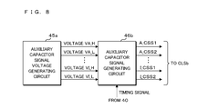
The display control circuit 4 b includes: an image signal input circuit 40; a gate driver control circuit 41; and a source driver control circuit 42 a. In addition, the display control circuit 4 a includes: an auxiliary capacitor signal voltage generating circuit 45 a that generates signal voltages determining the signal amplitudes of voltage signals applied to the auxiliary capacitor signal lines CS1 and CS2; and an auxiliary capacitor signal generating circuit (corresponding to an auxiliary capacitor signal line driving circuit) 46 b that generates voltage signals applied to the auxiliary capacitor signal lines CS1 and CS2 based on a DC signal voltage generated by the auxiliary capacitor signal voltage generating circuit 45 a and a timing signal transmitted from the image signal input circuit 40.
The auxiliary capacitor signal generating circuit 46 b is configured to drive the auxiliary capacitor signal lines CS1 and CS2 by using voltage signals having signal amplitudes different for the areas of A to I through the inter-auxiliary capacitor signal wiring CSLb. In such a case, by connecting the auxiliary capacitor signal lines CS1 and CS2 without segmented for each of the areas, the signal amplitude may be continuously changed between areas neighboring to each other.
FIG. 8 is an explanatory diagram that is used for describing voltages and signals outputted by the auxiliary capacitor signal voltage generating circuit 45 a and the auxiliary capacitor signal generating circuit 46 b. The auxiliary capacitor signal voltage generating circuit 45 a generates DC signal voltages corresponding to Va_H and Va_L illustrated in FIG. 4 of Embodiment 1 for each of the areas A to I. More specifically, the auxiliary capacitor signal voltage generating circuit 45 a generates voltages VA_H and VA_L having a same absolute value and different polarities (hereinafter, similarly) for the area A and generates voltages VB_H and VB_L for the area B, . . . , and generates voltages VI_H and VI_L for the area I. Thus, in this Embodiment 2, there are 18 kinds of signal voltages outputted by the auxiliary capacitor signal voltage generating circuit 45 a.
The auxiliary capacitor signal generating circuit 46 b generates signal voltages corresponding to the signals CSS1 and CSS2 illustrated in FIG. 4 of Embodiment 1 for each of the areas A to I based on a signal voltage transmitted from the auxiliary capacitor signal voltage generating circuit 45 a and a timing signal transmitted from the image signal input circuit 40. More specifically, the auxiliary capacitor signal generating circuit 46 b generates signals A_CSS1 and A_CSS2 based on voltages VA_H and VA_L for the area A, generates signals B_CSS1 and B_CSS2 based on voltages VB_H and VA_L for the area B, . . . , and generates signals I_CSS1 and I_CSS2 based on voltages VI_H and VI_L for the area I. Thus, in Embodiment 2, there are 18 kinds of voltage signals outputted by the auxiliary capacitor signal generating circuit 46 b.
Next, a simulation result at the time of changing the signal amplitudes of voltage signals applied to the auxiliary capacitor signal lines CS1 and CS2 according to the position of a pixel P on the display screen will be described.
FIG. 9 is a table that illustrates a relation between a position on the display screen and the amplitudes of signals applied to the auxiliary capacitor signal lines CS1 and CS2. FIG. 10 is a graph that illustrates a relation between a gray scale and luminance. FIG. 11 is a graph that illustrates a relation between a position on the display screen and a deviation amount of gamma characteristic.
A liquid crystal panel used for the simulation illustrated in FIGS. 9, 10, and 11 is a 60-inch type, and, as the planar dimension before curved, a vertical dimension is 748.44 mm, and a horizontal dimension is 1330.56 mm. The simulation is performed for a case where this liquid crystal panel curved in a cylindrical shape along the longitudinal direction (the lateral direction=the horizontal direction) such that the radius of curvature is 800 mm, and the display screen is convex toward the front side is regarded as the liquid crystal panel 100 b, and an observer observes the display screen from the center portion of the display screen while facing the display screen in front thereof. In addition, a viewing distance from the observer to the center portion of the display screen is 2245.32 mm. In such a case, a viewing angle at which the observer observes both ends of the display screen is about 47 degrees.
In the case illustrated in FIG. 9, as relative positions on the display screen, values of the positions of the left-end portion, the center portion, and the right-end portion of the display screen in the horizontal direction are set to −1.00, 0.00 and 1.00, and values of positions therebetween are uniformly assigned according to a distance along the display screen. Thus, positions having values of −1.00, 0.00, and 1.00 respectively correspond to a left-end portion of the area A, a center portion of the area E, and a right-end portion of the area I. In addition, positions having values of −0.75, −0.50, and −0.25 respectively correspond to the areas B, C, and D, and positions having values of 0.25, 0.50, and 0.75 respectively correspond to the areas F, G, and H.
The signal amplitudes of voltage signals applied to the auxiliary capacitor signal lines CS1 and CS2 in the areas are 4.50 V, 2.68 V, 2.14 V, 1.82 V, 1.50 V, 1.82 V, 2.14 V, 2.68 V, and 4.50 V for the areas A, B, C, D, E, F, G, H, and I. In other words, VA_H−VA_L=VI_H−VI_L=4.50 V, and VE_H−VE_L=1.50 V.
In addition, in FIGS. 10 and 11, “CONVENTIONAL” represents a case of a liquid crystal panel in which the signal amplitude of the voltage signals described above is fixed to 1.50 V.
Next, referring to FIG. 10, in the drawing, the horizontal axis represents a gray scale based on digital image data separated by the image signal input circuit 40, and the vertical axis represents luminance of which the maximum value is normalized to “1”. In the drawing, each curve illustrates a gamma characteristic representing the luminance observed at each relative position on the display screen with respect to the gray scale of an input signal. A dashed line illustrates a characteristic at a relative position having a value of 0.00 in a conventional liquid crystal panel and the liquid crystal panel 100 b according to the present invention and represents a standard characteristic having a γ value of 2.2. In addition, each of a broken line and a solid line represents characteristics of a relative position having a value of 075 in the conventional liquid crystal panel and the liquid crystal panel 100 b according to the present invention. In the liquid crystal panel 100 b according to the present invention, it is clearly disclosed that the γ value is closer to a characteristic of 2.2 than the conventional liquid crystal panel.
Here, a deviation amount between the gamma characteristic at the relative position having a value of 0.00 and a gamma characteristic at a relative position having a value other than 0.00 is represented using an index that is proportional to the area of a region surrounded by the characteristic curve at each relative position. For example, in the liquid crystal panel 100 b according to the present invention, a deviation amount of gamma characteristic at the relative position having a value of 0.75 corresponds to the area of a region surrounded by diagonal lines in FIG. 10.
Next, referring to FIG. 11, in the drawing, the horizontal axis represents a relative position on the display screen, and the vertical axis represents a deviation amount of gamma characteristic. In the drawing, a broken line and a solid line respectively represents the deviation amounts for a conventional liquid crystal panel and the liquid crystal panel 100 b according to the present invention. In the conventional liquid crystal panel, while the deviation amounts of gamma characteristic at relative position having values of −1.00 and 1.00 increase up to 30 on the whole, in the liquid crystal panel 100 b according to the present invention, the deviation amount of gamma characteristic at the same relative positions is settled into about 19. Also for the other relative positions, the liquid crystal panel 100 b according to the present invention has a deviation amount smaller than the conventional liquid crystal panel.
In addition, in Embodiment 2, while an example has been described in which two sub pixels SP1 and SP2 are included in the pixel P, the number of sub pixels is not limited to two but may be three or more, and the number of auxiliary capacitor signal lines may be increased according to the number of the sub pixels. For example, in a case where three sub pixels are included in one pixel, a voltage difference between the effective voltages of arbitrary two sub pixels may be changed as described above by using two auxiliary capacitor signal lines CS1 and CS2, and the effective voltage of the third sub pixel may be changed to be an intermediate voltage between the effective voltages of the two sub pixels. In a case where the effective voltage of the third sub pixel is changed according to a voltage signal supplied from the third auxiliary capacitor signal line, the auxiliary capacitor signal voltage generating circuit 45 a, for example, generates a third signal voltage, for example, that becomes VA_M, VB_M, . . . VI_M, and the auxiliary capacitor signal generating circuit 46 b generates a third voltage signal that becomes A_CSS3, B_CSS3, . . . I_CSS3, and the generated voltage signals may be applied to the third auxiliary capacitor signal line through the inter auxiliary capacitor signal wiring CSLb.
As described above, according to this Embodiment 2, the auxiliary capacitor signal generating circuit 46 b applies signals that have different amplitudes and inverted polarities according to the arrangement position of a pixel P in the row direction and/or the column direction of the matrix to the auxiliary capacitor signal lines CS1 and CS2 (a case where the third auxiliary capacitor signal line is added is included).
Accordingly, a voltage difference between the voltages applied to the liquid crystal layer 3 by two or more sub pixels starting from the sub pixels SP1 and SP2 included in the pixel P can be changed according to the arrangement position of a pixel P in the matrix.
(Embodiment 3)
While Embodiment 1 employs a form in which a voltage difference is caused between the voltages of the sub pixel electrodes 11 a and 11 b by applying mutually-different voltage signals to the auxiliary capacitor signal lines CS1 and CS2, Embodiment 3 employs a form in which source signals having mutually-different voltages are applied to sub pixel electrodes 11 a and 11 b through two source signal lines SL1 and SL2 arranged for each pixel P. In any of the forms, a voltage difference between voltages applied to a liquid crystal layer 3 by sub pixels SP1 and SP2 occurs.
FIG. 12 is a block diagram that illustrates an example of the configuration of a liquid crystal display apparatus according to Embodiment 3 of the present invention. FIG. 13 is an explanatory diagram that schematically illustrates a configuration partitioning a pixel P in a liquid crystal panel 100 c according to Embodiment 3 of the present invention. The liquid crystal display apparatus illustrated in FIG. 12 includes the liquid crystal panel 100 c in which pixels P are arranged in a matrix pattern in the vertical direction and the horizontal direction of a display screen. In the liquid crystal panel 100 c, the display screen is curved to be convex toward the front side. For the liquid crystal panel 100 c, representative three pixels P and signal lines relating to the pixels P will be focused in the illustration. Hereinafter, a same reference sign will be assigned to a configuration similar to that of Embodiment 1, and a part or the whole of description thereof will be omitted.
In the case illustrated in FIG. 13, the configuration of the sub pixels SP1 and SP2 included in a pixel P and the configuration of electrode pairs partitioning the sub pixels SP1 and SP2 are similar to those of the case according to Embodiment 1 illustrated in FIG. 2. Terminals of TFTs 15 a and 15 b are respectively connected to sub pixel electrodes 11 a and 11 b.
On one lateral side and the other lateral side of the pixel P in the horizontal direction, source signal lines SL1 and SL2 used for applying source signals to the sub pixel electrodes 11 a and 11 b through the TFTs 15 a and 15 b are linearly arranged in the vertical direction. The other ends of the TFTs 15 a and 15 b are connected to the source signal lines SL1 and SL2. Auxiliary capacitor opposing electrodes 14 a and 14 b are respectively connected to auxiliary capacitor signal lines CS1 and CS2. Gate electrodes of the TFTs 15 a and 15 b are connected to a scan signal line GL.
Referring to FIG. 12, the liquid crystal panel 100 c is divided into vertically-long areas of areas A to I in the horizontal direction. The liquid crystal display apparatus according to Embodiment 3 further includes: a gate driver GD; a source driver (corresponding to a data signal line driving circuit) SDb applying source signals to the source signal lines SL1, SL2, SL1, SL2, . . . SL1, SL2; an inter-auxiliary capacitor signal wiring CSLa; and a display control circuit 4 c that controls display using the liquid crystal panel 100 c by using the gate driver GD, the source driver SDb, and the inter-auxiliary capacitor signal wiring CSLa.
The display control circuit 4 c includes: an image signal input circuit 40; a gate driver control circuit 41; and a source driver control circuit 42 b that controls the source driver SDb. In addition, the display control circuit 4 c includes: an auxiliary capacitor signal generating circuit 46 c that generates voltage signals applied to the auxiliary capacitor signal lines CS1 and CS2; a contrast gray scale setting circuit (corresponding to an image signal converting unit) 43 that converts a gray scale value based on digital image data separated by the image signal input circuit 40 and supplies the converted gray scale value to the source driver control circuit 42 b; and a conversion table storing unit (corresponding to a storage unit) 44 a that stores a conversion table referred to by the contrast gray scale setting circuit 43. The auxiliary capacitor signal generating circuit 46 c is configured to drive the auxiliary capacitor signal lines CS1 and CS2 through the inter auxiliary capacitor signal wiring CSLa by using a DC voltage signal.
FIG. 14 is an explanatory diagram that is used for describing a conversion of a gray scale using the contrast gray scale setting circuit 43. The conversion table storing unit 44 a stores a conversion table (LUT=look up table) representing a correspondence relation between each of input gray scale values of 0 to 255 and an output gray scale value higher than the input gray scale value and an output gray scale value lower than the input gray scale value for each of areas A to I. The contrast gray scale setting circuit 43 converts an input gray scale value supplied from the image signal input circuit 40 into two high/low output gray scale values based on a timing signal supplied from the image signal input circuit 40 by referring to the conversion table corresponding to one of the areas A to I.
The two high/low output gray scale values converted from the input gray scale value are supplied to the source driver control circuit 42 b and are converted into two source signals having mutually-different high and low voltages, and the converted two source signals are applied to the source signal lines SL1 and SL2 through the source driver SDb. In this case, a voltage difference between the source signals applied to the source signal lines SL1 and SL2 is different for each of the areas A to I also in a case where the input gray scale value is the same and is optimally adjusted according to the gray scale value. In this way, the voltage difference between two source signals applied to the pixel P is reflected on a voltage difference between the voltages applied to the liquid crystal layer 3 by the sub pixels SP1 and SP2.
In addition, in this Embodiment 3, while an example has been described in which two sub pixels SP1 and SP2 are included in the pixel P, the number of sub pixels is not limited to two but may be three or more, and the number of source signal lines may be increased according to the number of the sub pixels. For example, in a case where three sub pixels are included in one pixel, a voltage difference between the effective voltages of arbitrary two sub pixels may be changed as described above by using two source signal lines SL1 and SL2, and the effective voltage of the third sub pixel may be changed to be an intermediate voltage between the effective voltages of the two sub pixels by using the third source signal line and a third TFT.
As described above, according to this Embodiment 3, in the electrode pair partitioning the sub pixels SP1 and SP2 included in the pixel P, the electrode pair of the sub pixel electrode 11 a and the opposing electrode 21 facing each other through the liquid crystal layer 3 and the electrode pair of the sub pixel electrode 11 b and the opposing electrode 21 are included. Then, source signals are applied to the sub pixel electrodes 11 a and 11 b from the source signal lines SL1 and SL2 through the TFTs 15 a and 15 b. In addition, a source signal is applied to the sub pixel electrodes of the third sub pixel from the source signal lines SL1 and SL2 (or the third source signal line) through the third TFT.
Accordingly, voltages having mutually-different magnitudes can be applied to the liquid crystal layer 3 by using two or more sub pixels starting from the sub pixels SP1 and SP2 included in each pixel P.
In addition, according to Embodiment 3, for each of nine areas acquired by dividing the arrangement positions of pixels P in the row direction and/or the column direction of the matrix, correspondence relations between the gray scale value relating to image data and a plurality of gray scale values having mutually-different magnitudes are stored in the conversion table storing unit 44 a in advance. Then, the contrast gray scale setting circuit 43 converts the gray scale value based on image data separated from an image signal received by the image signal input circuit 40 into a plurality of gray scale values having mutually-different magnitudes based on the stored content of the conversion table storing unit 44 a, and the source driver SDb applies source signals corresponding to the plurality of gray scale values converted by the source driver SDb to the source signal lines SL1 and SL2 (or the third source signal line).
Accordingly, a voltage difference between the voltages applied to the liquid crystal layer 3 by two or more sub pixels starting from the sub pixels SP1 and SP2 included in a pixel P can be changed according to the divided position of the pixel P in the matrix.
(Embodiment 4)
While Embodiment 2 employs a form in which the viewing distance of an observer and the curvature of the liquid crystal panel 100 b are not considered in a case where the amplitudes of the signals CSS1 and CSS2 are changed according to the position of the pixel P, Embodiment 4 employs a form in which, on top of the consideration of the viewing distance of an observer and/or the curvature of the liquid crystal panel 100 b, the amplitudes of the signals CSS1 and CSS2 are changed according to the position of the pixel P.
FIG. 15 is a block diagram that illustrates an example of the configuration of a liquid crystal display apparatus according to Embodiment 4 of the present invention. The liquid crystal display apparatus includes a liquid crystal panel 100 b in which pixels P are arranged in a matrix pattern in the vertical direction and the horizontal direction of a display screen. The liquid crystal panel 100 b is the same as that used in Embodiment 2. Hereinafter, a same reference sign will be assigned to a configuration similar to that of Embodiments 1 and 2, and a part or the whole of description thereof will be omitted.
The liquid crystal display apparatus according to Embodiment 4 includes: a gate driver GD; a source driver SD; an inter-auxiliary capacitor signal wiring CSLb; and a display control circuit 4 d that controls display using the liquid crystal panel 100 b by using the gate driver GD, the source driver SD, and the inter-auxiliary capacitor signal wiring CSLb.
The display control circuit 4 d includes: an image signal input circuit 40; a gate driver control circuit 41; and a source driver control circuit 42 a. In addition, the display control circuit 4 d includes: an auxiliary capacitor signal voltage generating circuit 45 b that generates the voltages VA_H, VA_L, VB_H, VB_L, . . . , VI_H, VI_L (see FIG. 8) described above; and an auxiliary capacitor signal generating circuit (corresponding to an auxiliary capacitor signal line driving circuit) 46 b that generates voltage signals applied to the auxiliary capacitor signal lines CS1 and CS2 based on a DC signal voltage generated by the auxiliary capacitor signal voltage generating circuit 45 b and a timing signal transmitted from the image signal input circuit 40.
In addition, the display control circuit 4 d includes: a signal voltage storing unit 47 that stores a plurality of pieces of information designating the magnitudes of voltages VA_H, VA_L, VB_H, VB_L, . . . , VI_H, VI_L to be generated by the auxiliary capacitor signal voltage generating circuit 45 b; and a signal voltage determining unit 48 that receives signal voltage determination data supplied from the outside and determines one piece of information to be read from the signal voltage storing unit 47.
The auxiliary capacitor signal voltage generating circuit 45 b reads the information determined by the signal voltage determining unit 48 from the signal voltage storing unit 47 and generates voltages VA_H, VA_L, VB_H, VB_L, . . . , VI_H, VI_L of magnitudes designated by the read information. In other words, the amplitudes of the voltage signals generated by the auxiliary capacitor signal generating circuit 46 b for each area are changed according to the signal voltage determination data supplied from the outside. In this way, a voltage difference between the voltages applied to the liquid crystal layer 3 by two or more sub pixels starting from the sub pixels SP1 and SP2 and a brightness difference or a luminance difference between the two or more sub pixels are not only changed according to the arrangement position of the pixel P but also changed according to the signal voltage determination data supplied from the outside.
In addition, the signal voltage determining unit 48 may be configured to supply information used for selecting one piece of information from among the plurality of pieces of information stored in the signal voltage storing unit 47 to the auxiliary capacitor signal voltage generating circuit 45 b, and the auxiliary capacitor signal voltage generating circuit 45 b may read one piece of information from among the plurality of pieces of information stored in the signal voltage storing unit 47 based on the information supplied from the signal voltage determining unit 48.
Among the voltages VA_H, VB_H, . . . , VI_H, based on the information stored in the signal voltage storing unit 47, the voltages VA_H and VI_H are maximum, and the voltage VE_H is minimum, and the voltages of VA_H to VE_H and the voltages of VI_H to VE_H are decreased in a stepped manner. This is similarly applied to the voltages VA_L, VB_L, . . . , VI_L having the same absolute values as those of the voltages VA_H, VB_H, . . . VI_H and having different polarities.
Such voltages are determined in advance such that the viewing angle dependency of gamma characteristics is appropriately improved over all the area of the display screen. In such a case, according to “large/small” of the magnitudes of VA_H−VA_L and VI_H−VI_L, a voltage difference between the voltages applied to the liquid crystal layer 3 by the sub pixels SP1 and SP2 of the pixels P disposed at both end portions of the display screen become “large/small”, and the improvement factor of the viewing angle dependency of gamma characteristic becomes “large/small”. According to “large/small” of the magnitudes of VA_H−VA_L and VI_H−VI_L corresponding to the both end portions of the display screen, the magnitude of VE_H−VE_L corresponding to the center portion of the display screen may be configured to be “large/small”, or the magnitude of VE_H−VE_L may be configured to be constant.
Next, signal voltage determination data will be described.
FIG. 16A is an explanatory diagram that is used for describing an angle formed by a sight line for a liquid crystal panel 100 b curved to be convex toward the front side and a normal line of a display screen. FIG. 16B is an explanatory diagram that is used for describing an angle formed by a sight line for a liquid crystal panel 100 e curved to be concave toward the front side and a normal line of a display screen. The two liquid crystal panels 100 e illustrated in FIG. 16B are the same, and only the positions of the observer with respect to the display screen are different.
In the liquid crystal panels 100 b and 100 e illustrated in FIGS. 16A and 16B, the display screens are curved in a cylindrical shape along the longitudinal direction (the lateral direction=the horizontal direction) so as to be convex and concave toward the front side. The curvature center of each of the liquid crystal panels 100 b and 100 e is represented as center O. An observer is located on a segment joining the center portion of the display screen and the center O or an extension of this segment and faces the display screen in front thereof. Here, a separation distance between the center portion of the display screen and location of the observer, in other words, the viewing distance is denoted by L, and the radius of curvature of the display screen is denoted by R. In a case where the observation target position is an end portion on the display screen, an angle formed by the normal line of the display screen at the observation target position and the sight line of the observer is denoted by δ.
As illustrated in FIG. 16A, in a case where the liquid crystal panel 100 b is convex toward the front side, when the value of R is fixed, it is apparent that the value of δ increases as the value of L decreases. To the contrary, when the value of L is fixed, it is apparent that the value of δ increases as the value of R decreases. Here, there is a limit when the value of δ is 90 degrees. As the value of δ increases, the problem of the viewing angle dependency of gamma characteristic becomes marked, which is described as above. Accordingly, in a case where the “large/small” of the value of the signal voltage determination data is associated with “large/small” of the value of L that is the viewing distance or the value of R that is the radius of curvature of the display screen, as the value of the signal voltage determination data increases (or decreases), information designating VA_H, VA−L and VI_H, VI−L having a smaller (or larger) absolute value is determined by the signal voltage determining unit 48.
On the other hand, as illustrated in FIG. 16B, in a case where the liquid crystal panel 100 e is concave toward the front side, when the value of R is fixed, the value of δ decreases (see the right case illustrated in the drawing) as the value of L increases from 0 to the value of R, and as the value of L further increases from the value of R, the value of δ increases (see the left case illustrated in the drawing). To the contrary, when the value of L is fixed, the value of δ decreases (see the left case illustrated in the drawing) as the value of R increases from a value less than L to the value of L, and as the value of R further increases from the value of L, the value of δ increases (see the right case illustrated in the drawing).
Accordingly, in a case where the “large/small” of the value of the signal voltage determination data is associated with the “large/small” of the value of L, when L<R, as the value of the signal voltage determination data becomes larger (or smaller), the information designating VA_H, VA−L and VI_H, VI−L having a smaller (larger) absolute value is determined. On the other hand, when L>R, as the value of the signal voltage determination data becomes larger (or smaller), the information designating VA_H, VA−L and VI_H, VI−L having a larger (smaller) absolute value is determined.
In contrast to this, in a case where the “large/small” of the value of the signal voltage determination data is associated with “large/small” of the value of R, when R<L, as the value of the signal voltage determination data becomes larger (or smaller), the information designating VA_H, VA−L and VI_H, VI−L having a smaller (larger) absolute value is determined. On the other hand, when R>L, as the value of the signal voltage determination data becomes larger (or smaller), the information designating VA_H, VA−L and VI_H, VI−L having a larger (smaller) absolute value is determined.
As above, it is preferable to switch the stored content of the signal voltage storing unit 47 in accordance with whether the liquid crystal panel is convex or concave toward the front side. In addition, it is more preferable to further switch the stored content of the signal voltage storing unit 47 in accordance with the correspondence of the signal voltage determination data with the value of R or the value or L. Furthermore, in a case where the liquid crystal panel is concave toward the front side, it is preferable that the stored content of the signal voltage storing unit 47 is further switched according to a difference of the magnitude relation between the value of R and the value of L. In other words, by switching the stored content of the signal voltage storing unit 47, in any of the cases described above, based on the signal voltage determination data, one piece of information that is optimal for the radius of curvature of the liquid crystal panel and/or the viewing distance can be determined from among a plurality of pieces of information stored in the signal voltage storing unit 47.
In this Embodiment 4, while a case has been described in which the signal voltage determining unit 48 acquires signal voltage determination data from the outside, in a case where the radius of curvature and the viewing distance are determined to be fixed, the signal voltage determining unit 48 may not be used. In such a case, the signal voltage storing unit 47 may store optimal information that is based on the radius of curvature and the viewing distance determined in advance.
As described above, according to this Embodiment 4, in accordance with the radius R of curvature of the display screen of the liquid crystal panel 100 b or 100 e, a voltage difference between the voltages applied to the liquid crystal layer 3 in accordance with the two or more sub pixels starting from the sub pixels SP1 and SP2 or a brightness difference or a luminance difference between the two or more sub pixels is different.
Accordingly, in order to compensate for a change in the degree of influence of the viewing angle dependency of gamma characteristic according to the curvature of the display screen, the improvement factor of the viewing angle dependency of gamma characteristic can be changed. In addition, also in a case where the radius R of curvature of the display screen is not constant in the plane, a similar effect can be acquired.
In addition, according to Embodiment 4, in accordance with the viewing distance L from the center portion of the display screen of the liquid crystal panel 100 b or 100 e to a position separate in the direction of the normal line on the front side of the display screen, a voltage difference between the voltages applied to the liquid crystal layer 3 in accordance with two or more sub pixels starting from the sub pixels SP1 and SP2 or a brightness difference or a luminance difference between the two or more sub pixels is different.
Accordingly, in order to compensate for a change in the degree of influence of the viewing angle dependency of gamma characteristic according to the viewing distance L for the display screen, the improvement factor of the viewing angle dependency of gamma characteristic can be changed.
In addition, according to Embodiment 4, as the radius of curvature of the display screen of the liquid crystal panel 100 b curved to be convex toward the front side is smaller (in other words, the curvature is larger) or as the viewing distance is shorter, a voltage difference between the voltages applied to the liquid crystal layer 3 in accordance with the two or more sub pixels staring from the sub pixels SP1 and SP2 or a brightness difference or a luminance difference between the two or more sub pixels becomes larger.
Accordingly, in order to compensate for a change in the degree of influence of the viewing angle dependency of gamma characteristic to “large/small” according to “large/small” of the curvature of the display screen or “short/long” of the viewing distance for the display screen, the improvement factor of the viewing angle dependency of gamma characteristic can be changed to “large/small”.
(Embodiment 5)
While Embodiment 3 employs a form in which the viewing distance of an observer and the curvature of the liquid crystal panel 100 b are not considered in a case where a voltage difference between the source signals applied to the sub pixel electrodes 11 a and 11 b is changed according to the position of the pixel P, Embodiment 5 employs a form in which, on top of the consideration of the viewing distance of an observer and/or the curvature of the liquid crystal panel 100 b, a voltage difference between the source signals applied to the sub pixel electrodes 11 a and 11 b is changed according to the position of the pixel P.
FIG. 17 is a block diagram that illustrates an example of the configuration of a liquid crystal display apparatus according to Embodiment 5 of the present invention. The liquid crystal display apparatus includes a liquid crystal panel 100 c in which pixels P are arranged in a matrix pattern in the vertical direction and the horizontal direction of a display screen. The liquid crystal panel 100 c is the same as that used in Embodiment 3. Hereinafter, a same reference sign will be assigned to a configuration similar to that of Embodiments 1 and 3, and a part or the whole of description thereof will be omitted.
A liquid crystal display apparatus according to Embodiment 5 includes: a gate driver GD; a source driver SDb; an inter-auxiliary capacitor signal wiring CSLa; and a display control circuit 4 e that controls display using the liquid crystal panel 100 c by using the gate driver GD, the source driver SDb, and the inter auxiliary capacitor signal wiring CSLa.
The display control circuit 4 e includes: an image signal input circuit 40; a gate driver control circuit 41; a source driver control circuit 42 b; an auxiliary capacitor signal generating circuit 46 c; a contrast gray scale setting circuit 43; a conversion table storing unit 44 b that stores a plurality of conversion tables referred to by the contrast gray scale setting circuit 43; and a conversion table determining unit 49 that receives conversion table determination data from the outside and determines one conversion table to be referred to by the conversion table storing unit 44 b.
The contrast gray scale setting circuit 43 refers to the conversion table determined by the conversion table determining unit 49 from the conversion table storing unit 44 b and performs a conversion of a gray scale value illustrated in FIG. 14 according to Embodiment 3. In other words, a voltage difference between source signals applied from the source driver control circuit 42 b to the source signal lines SL1 and SL2 through the source driver SDb is changed according to the conversion table determination data supplied from the outside.
In addition, the conversion table determining unit 49 may supply information used for determining one conversion table among a plurality of pieces of conversion table information stored in the conversion table storing unit 44 b to the contrast gray scale setting circuit 43, and the contrast gray scale setting circuit 43 may refer to one conversion table among the plurality of conversion tables stored in the conversion table storing unit 44 b based on the information supplied from the conversion table determining unit 49.
Next, the conversion tables and the conversion table determination data will be described.
FIG. 18 is an explanatory diagram that illustrates an example of the stored content of the conversion table storing unit 44 b. FIG. 19 is an explanatory diagram that illustrates an example of the stored content of another conversion table storing unit. In the conversion table storing unit 44 b and the another conversion table storing unit 44 c illustrated in FIGS. 18 and 19, n conversion tables (LUT) according to Embodiment 3 illustrated in FIG. 14 are stored. The another conversion table storing unit 44 c is used by replacing the conversion table storing unit 44 b in accordance with a content represented by the conversion table determination data.
In a case where the value of the conversion table determination data corresponds to the value of L that is the viewing distance illustrated in FIG. 16A or 16B according to Embodiment 4, one of n conversion tables stored in the conversion table storing unit 44 b is determined as a conversion table to be referred to by the contrast gray scale setting circuit 43 in accordance with “large/small” of the value of L. Similarly, in a case where the value of the conversion table determination data corresponds to the value of R that is the radius of curvature illustrated in FIG. 16A or 16B, one of the n conversion tables stored in the another conversion table storing unit 44 c is determined as a conversion table to be referred to by the contrast gray scale setting circuit 43 in accordance with “large/small” of the value of R.
Operations after the determination of one conversion table to be referred to from the contrast gray scale setting circuit 43 are similar to those of the case of Embodiment 3 as a whole. As a result, a voltage difference between source signals applied to the source signal lines SL1 and SL2 is different for each of the areas A to I, and is optimally adjusted according to the value of L that is the viewing distance or the value of R that is the radius of curvature. Then, a voltage difference between the source signals applied to the pixel P is reflected on a voltage difference between the voltages applied to the liquid crystal layer 3 by the sub pixels SP1 and SP2.
As described above, according to this Embodiment 5, in accordance with the radius R of curvature of the display screen of the liquid crystal panel 100 c, a voltage difference between the voltages applied to the liquid crystal layer 3 in accordance with the two or more sub pixels starting from the sub pixels SP1 and SP2 or a brightness difference or a luminance difference between the two or more sub pixels is different.
Accordingly, in order to compensate for a change in the degree of influence of the viewing angle dependency of gamma characteristic according to the curvature of the display screen, the improvement factor of the viewing angle dependency of gamma characteristic can be changed.
In addition, according to Embodiment 5, in accordance with the viewing distance L for the display screen of the liquid crystal panel 100 c, a voltage difference between the voltages applied to the liquid crystal layer 3 in accordance with two or more sub pixels starting from the sub pixels SP1 and SP2 or a brightness difference or a luminance difference between the two or more sub pixels is different according to the viewing distance L of the display screen of the liquid crystal panel 100 c.
Accordingly, in order to compensate for a change in the degree of influence of the viewing angle dependency of gamma characteristic according to the viewing distance L for the display screen, the improvement factor of the viewing angle dependency of gamma characteristic can be changed.
It is to be noted that, as used herein and in the appended claims, the singular forms “a”, “an”, and “the” include plural referents unless the context clearly dictates otherwise.
The embodiments described here are examples in all the points and should not be considered for the purpose of limitations. The scope of the present invention is not the meaning described above but is intended to include a scope that is disclosed in the claims and is equivalent to the claims and all the changes within the scope. In addition, the technical aspects described in the embodiments may be combined together.

Claims (22)

The invention claimed is:
1. A liquid crystal display apparatus, comprising:
a liquid crystal layer; and
a plurality of electrode pairs used for applying voltages to the liquid crystal layer,
wherein pixels partitioned to include the electrode pairs are arranged in a matrix pattern,
at least two sub pixels partitioned to include at least one of the electrode pairs are included in each of the pixels, and
a voltage difference between a voltage applied to the liquid crystal layer by the electrode pairs partitioning one sub pixel of the at least two sub pixels included in one pixel and a voltage applied to the liquid crystal layer by the electrode pairs partitioning another sub pixel of the at least two sub pixels included in the one pixel is different according to an arrangement position of the pixel in a row direction and/or a column direction of the matrix.
2. The liquid crystal display apparatus according to claim 1, wherein
the voltage difference increases as the arrangement position of the pixel is further separate from a center portion in a row direction and/or a column direction of the matrix.
3. The liquid crystal display apparatus according to claim 2, further comprising:
a liquid crystal panel which has the liquid crystal layer and the electrode pairs and includes a display screen curved toward a front side,
wherein the voltage difference is different according to a curvature of the display screen of the liquid crystal panel.
4. The liquid crystal display apparatus according to claim 3, wherein
the display screen of the liquid crystal panel is curved to be convex toward the front side, and
the voltage difference is larger as the curvature is larger.
5. The liquid crystal display apparatus according to claim 3, wherein
the voltage difference is different according to a distance from the center portion of the display screen of the liquid crystal panel to a position separate in a direction of a normal line on the front side of the display screen.
6. The liquid crystal display apparatus according to claim 5, wherein
the display screen of the liquid crystal panel is curved to be convex toward the front side, and
the voltage difference is larger as the distance is shorter.
7. The liquid crystal display apparatus according to claim 1, wherein
each of the at least two sub pixels is partitioned to include an electrode pair of a sub pixel electrode and an opposing electrode facing each other through the liquid crystal layer,
further comprising:
a switching element disposed with respect to each of the at least two sub pixels; and
at least two data signal lines used for applying data signals to the sub pixel electrodes through the switching elements.
8. The liquid crystal display apparatus according to claim 7, further comprising:
a reception unit that receives image data;
a storage unit that stores, for each of divisions acquired by dividing arrangement positions of the pixels into a plurality of parts, a correspondence relation between a gray scale value and a plurality of the gray scale values having mutually-different magnitudes;
an image signal converting unit that converts a gray scale value based on the image data received by the reception unit into a plurality of gray scale values having mutually-different magnitudes based on a division to which the arrangement position of the pixel belongs and a stored content of the storage unit; and
a data signal line driving circuit that applies data signals according to the plurality of gray scale values converted by the image signal converting unit to the at least two data signal lines.
9. The liquid crystal display apparatus according to claim 1, wherein
each of the at least two sub pixels is partitioned to include an electrode pair of a sub pixel electrode and an opposing electrode facing each other through the liquid crystal layer, an insulating layer, and an electrode pair of an auxiliary capacitor electrode and an auxiliary capacitor opposing electrode facing each other through the insulating layer, and
the sub pixel electrode and the auxiliary capacitor electrode are electrically connected,
further comprising:
at least two auxiliary capacitor signal lines used for applying voltage signals to the auxiliary capacitor opposing electrode.
10. The liquid crystal display apparatus according to claim 9, further comprising:
an auxiliary capacitor signal line driving circuit that applies voltage signals to the auxiliary capacitor signal lines,
wherein the voltage signals applied to specific two auxiliary capacitor signal lines by the auxiliary capacitor signal line driving circuit have opposite polarities and have amplitudes different according to the arrangement position of the pixel.
11. A liquid crystal display apparatus, comprising:
a liquid crystal layer; and
a plurality of electrode pairs used for applying a voltage to the liquid crystal layer,
wherein pixels partitioned to include the electrode pairs are arranged in a matrix pattern,
at least two sub pixels partitioned to include at least one of the electrode pairs are included in each of the pixels, and
a brightness difference or a luminance difference between a brightness or a luminance of one sub pixel of the at least two sub pixels included in one pixel and a brightness or a luminance of another sub pixel of the at least two sub pixels included in the one pixel is different according to an arrangement position of the pixel in a row direction and/or a column direction of the matrix.
12. The liquid crystal display apparatus according to claim 11, wherein
the brightness difference or the luminance difference increases as the arrangement position of the pixel is further separate from a center portion in a row direction and/or a column direction of the matrix.
13. The liquid crystal display apparatus according to claim 12, further comprising:
a liquid crystal panel which has the liquid crystal layer and the electrode pairs and includes a display screen curved toward a front side,
wherein the brightness difference or the luminance difference is different according to a curvature of the display screen of the liquid crystal panel.
14. The liquid crystal display apparatus according to claim 13, wherein
the display screen of the liquid crystal panel is curved to be convex toward the front side, and
the brightness difference or the luminance difference is larger as the curvature is larger.
15. The liquid crystal display apparatus according to claim 13, wherein
the brightness difference or the luminance difference is different according to a distance from the center portion of the display screen of the liquid crystal panel to a position separate in a direction of a normal line on the front side of the display screen.
16. The liquid crystal display apparatus according to claim 15, wherein
the display screen of the liquid crystal panel is curved to be convex toward the front side, and
the brightness difference or the luminance difference is larger as the distance is shorter.
17. The liquid crystal display apparatus according to claim 11, wherein
each of the at least two sub pixels is partitioned to include an electrode pair of a sub pixel electrode and an opposing electrode facing each other through the liquid crystal layer,
further comprising:
a switching element disposed with respect to each of the at least two sub pixels; and
at least two data signal lines used for applying data signals to the sub pixel electrodes through the switching elements.
18. The liquid crystal display apparatus according to claim 17, further comprising:
a reception unit that receives image data;
a storage unit that stores, for each of divisions acquired by dividing arrangement positions of the pixels into a plurality of parts, a correspondence relation between a gray scale value and a plurality of the gray scale values having mutually-different magnitudes;
an image signal converting unit that converts a gray scale value based on the image data received by the reception unit into a plurality of gray scale values having mutually-different magnitudes based on a division to which the arrangement position of the pixel belongs and a stored content of the storage unit; and
a data signal line driving circuit that applies data signals according to the plurality of gray scale values converted by the image signal converting unit to the at least two data signal lines.
19. The liquid crystal display apparatus according to claim 11, wherein
each of the at least two sub pixels is partitioned to include an electrode pair of a sub pixel electrode and an opposing electrode facing each other through the liquid crystal layer, an insulating layer, and an electrode pair of an auxiliary capacitor electrode and an auxiliary capacitor opposing electrode facing each other through the insulating layer, and
the sub pixel electrode and the auxiliary capacitor electrode are electrically connected,
further comprising:
at least two auxiliary capacitor signal lines used for applying voltage signals to the auxiliary capacitor opposing electrode.
20. The liquid crystal display apparatus according to claim 19, further comprising:
an auxiliary capacitor signal line driving circuit that applies voltage signals to the auxiliary capacitor signal lines,
wherein the voltage signals applied to specific two auxiliary capacitor signal lines by the auxiliary capacitor signal line driving circuit have opposite polarities and have amplitudes different according to the arrangement position of the pixel.
21. A method of driving a liquid crystal display apparatus which comprises a liquid crystal layer and a plurality of electrode pairs used for applying voltages to the liquid crystal layer, and in which pixels partitioned to include the electrode pairs are arranged in a matrix pattern and at least two sub pixels partitioned to include one or two electrode pairs are included in each of the pixels,
wherein a voltage difference between a voltage applied to the liquid crystal layer by the electrode pairs partitioning one sub pixel of the at least two sub pixels included in one pixel and a voltage applied to the liquid crystal layer by the electrode pairs partitioning another sub pixel of the at least two sub pixels included in the one pixel is different according to an arrangement position of the pixel in a row direction and/or a column direction of a matrix.
22. A method of driving a liquid crystal display apparatus which comprises a liquid crystal layer and a plurality of electrode pairs used for applying voltages to the liquid crystal layer, and in which pixels partitioned to include the electrode pairs are arranged in a matrix pattern and at least two sub pixels partitioned to include one or two electrode pairs are included in each of the pixels,
wherein a brightness difference or a luminance difference between a brightness or a luminance of one sub pixel of the at least two sub pixels included in one pixel and a brightness or a luminance of another sub pixel of the at least two sub pixels included in the one pixel is different according to an arrangement position of the pixel in a row direction and/or a column direction of the matrix.
US15/329,492 2014-12-18 2014-12-18 Liquid crystal display apparatus and method of driving liquid crystal display apparatus Expired - Fee Related US10345641B2 (en)

Applications Claiming Priority (1)

Application Number Priority Date Filing Date Title
PCT/JP2014/083608 WO2016098232A1 (en) 2014-12-18 2014-12-18 Liquid crystal display device and method for driving liquid crystal display device

Publications (2)

Publication Number Publication Date
US20170322449A1 US20170322449A1 (en) 2017-11-09
US10345641B2 true US10345641B2 (en) 2019-07-09

Family

ID=56126152

Family Applications (1)

Application Number Title Priority Date Filing Date
US15/329,492 Expired - Fee Related US10345641B2 (en) 2014-12-18 2014-12-18 Liquid crystal display apparatus and method of driving liquid crystal display apparatus

Country Status (4)

Country Link
US (1) US10345641B2 (en)
JP (1) JP6220466B2 (en)
CN (1) CN106687854B (en)
WO (1) WO2016098232A1 (en)

Families Citing this family (7)

* Cited by examiner, † Cited by third party
Publication number Priority date Publication date Assignee Title
CN107123402B (en) * 2017-05-26 2019-08-23 京东方科技集团股份有限公司 A kind of display device and its control method
JP2019070770A (en) * 2017-10-11 2019-05-09 シャープ株式会社 Liquid crystal display and electronic apparatus
CN107861278B (en) * 2017-12-26 2020-01-03 昆山龙腾光电股份有限公司 Liquid crystal display device having a plurality of pixel electrodes
US11763748B2 (en) * 2019-10-21 2023-09-19 Hewlett-Packard Development Company, L.P. Pixel-addressable display having curvable area
CN111323956A (en) * 2020-04-08 2020-06-23 Tcl华星光电技术有限公司 Liquid crystal display panel, display module and electronic device
CN112099276A (en) * 2020-09-23 2020-12-18 惠科股份有限公司 Driving array substrate, display panel and display device
CN114220404B (en) * 2021-12-11 2022-11-15 重庆惠科金渝光电科技有限公司 Method and device for improving display uniformity and terminal equipment

Citations (38)

* Cited by examiner, † Cited by third party
Publication number Priority date Publication date Assignee Title
US5900863A (en) 1995-03-16 1999-05-04 Kabushiki Kaisha Toshiba Method and apparatus for controlling computer without touching input device
US20030227429A1 (en) * 2002-06-06 2003-12-11 Fumikazu Shimoshikiryo Liquid crystal display
US20050059488A1 (en) 2003-09-15 2005-03-17 Sony Computer Entertainment Inc. Method and apparatus for adjusting a view of a scene being displayed according to tracked head motion
JP2006133577A (en) 2004-11-08 2006-05-25 Sharp Corp Substrate for liquid crystal display device, and liquid crystal display device equipped with same, and method for driving the liquid crystal display device
JP2006276120A (en) 2005-03-28 2006-10-12 Seiko Epson Corp Electrooptical apparatus, display control apparatus, display control method and display control program
US20070132895A1 (en) 2005-12-12 2007-06-14 Novatek Microelectronics Corp. Compensation device for non-uniform regions in flat panel display and method thereof
US20080049052A1 (en) 2004-09-30 2008-02-28 Sharp Kabushiki Kaisha Liquid Crystal Display
US20090109015A1 (en) 2007-10-31 2009-04-30 Fujitsu Limited Display device with anti-crime security function
US20090213053A1 (en) 2005-09-22 2009-08-27 Sharp Kabushiki Kaisha Liquid Crystal Display Device
WO2011065058A1 (en) 2009-11-30 2011-06-03 シャープ株式会社 Substrate for liquid crystal display device, liquid crystal display device, and method for driving liquid crystal display device
US20110221760A1 (en) * 2008-12-25 2011-09-15 Sharp Kabushiki Kaisha Display device and method for driving same
US20110234605A1 (en) 2010-03-26 2011-09-29 Nathan James Smith Display having split sub-pixels for multiple image display functions
US20110242149A1 (en) * 2008-12-10 2011-10-06 Sharp Kabushiki Kaisha Liquid crystal display device
US20120075166A1 (en) 2010-09-29 2012-03-29 Samsung Electronics Co. Ltd. Actuated adaptive display systems
WO2012093630A1 (en) 2011-01-07 2012-07-12 シャープ株式会社 Liquid crystal display device
US20120256971A1 (en) 2011-04-08 2012-10-11 Samsung Mobile Display Co., Ltd. Organic light emitting diode display and method of driving the same
US20120306936A1 (en) 2011-05-31 2012-12-06 Samsung Mobile Display Co., Ltd. Organic light emitting display and method of driving the same
US20130021240A1 (en) 2011-07-18 2013-01-24 Stmicroelectronics (Rousset) Sas Method and device for controlling an apparatus as a function of detecting persons in the vicinity of the apparatus
US20130027439A1 (en) 2011-07-27 2013-01-31 Samsung Electronics Co., Ltd. Display apparatus
US20130222236A1 (en) 2012-02-24 2013-08-29 Research In Motion Limited Handheld device with notification message viewing
US20140118255A1 (en) 2012-10-25 2014-05-01 Bryed Billerbeck Graphical user interface adjusting to a change of user's disposition
US20140191933A1 (en) 2013-01-07 2014-07-10 Au Optronics Corporation Adjustable viewing angle display device and method for driving the same
US20150109268A1 (en) 2013-10-23 2015-04-23 Au Optronics Corporation Pixel unit, pixel array and liquid crystal display panel
US20150116301A1 (en) 2012-12-07 2015-04-30 Sakai Display Products Corporation Liquid Crystal Display Device and Method for Driving the Liquid Crystal Display Device
US20150316824A1 (en) 2013-04-05 2015-11-05 Sakai Display Products Corporation Active Matrix Circuit, Method of Manufacturing Active Matrix Circuit and Image Display Apparatus
US20150357351A1 (en) 2014-06-09 2015-12-10 Shenzhen China Star Optoelectronics Technology Co. Ltd. Array substrate and curved display device
US20150379948A1 (en) 2013-02-19 2015-12-31 Sakai Display Products Corporation Display Apparatus
US20160012793A1 (en) 2013-05-29 2016-01-14 Sakai Display Products Corporation Display Apparatus
US20160078819A1 (en) 2014-09-16 2016-03-17 Samsung Display Co., Ltd. Liquid crystal display device and driving method thereof
US20160104435A1 (en) 2014-01-22 2016-04-14 Sakai Display Products Corporation Display Apparatus
US20160140907A1 (en) 2014-01-22 2016-05-19 Sakai Display Products Corporation Display Apparatus
US20160202758A1 (en) 2015-01-12 2016-07-14 Dell Products, L.P. Immersive environment correction display and method
US20160225333A1 (en) 2009-11-17 2016-08-04 Samsung Display Co. Ltd. Liquid crystal display
US20170031434A1 (en) 2015-07-30 2017-02-02 Dell Products L.P. Display device viewing angle compensation system
US20170110059A1 (en) 2015-10-16 2017-04-20 Samsung Display Co., Ltd. Display device and method of controlling the same
US20170329399A1 (en) 2015-01-30 2017-11-16 Hewlett-Packard Development Company, L.P. Electronic display illumination
US20180096655A1 (en) 2016-09-30 2018-04-05 Lg Display Co., Ltd. Organic light emitting display device and method of controlling same
US20180188585A1 (en) 2015-06-23 2018-07-05 Sakai Display Products Corporation Liquid Crystal Display Apparatus and Method for Driving Liquid Crystal Display Apparatus

Family Cites Families (8)

* Cited by examiner, † Cited by third party
Publication number Priority date Publication date Assignee Title
US20100182345A1 (en) * 2006-08-10 2010-07-22 Fumikazu Shimoshikiryoh Liquid crystal display
JP2008158286A (en) * 2006-12-25 2008-07-10 Sharp Corp Liquid crystal display device
WO2008111490A1 (en) * 2007-03-15 2008-09-18 Sharp Kabushiki Kaisha Liquid crystal display device
RU2012100253A (en) * 2009-06-11 2013-07-20 Шарп Кабусики Кайся LIQUID DISPLAY DEVICE
KR101699398B1 (en) * 2009-10-28 2017-01-25 삼성디스플레이 주식회사 Liquid crystal display
WO2011155300A1 (en) * 2010-06-08 2011-12-15 シャープ株式会社 Display panel and liquid crystal display device
TWI533270B (en) * 2014-03-27 2016-05-11 友達光電股份有限公司 Display panel and driving method thereof
CN103941508B (en) * 2014-04-10 2017-02-08 深圳市华星光电技术有限公司 Pixel structure and liquid crystal display device

Patent Citations (79)

* Cited by examiner, † Cited by third party
Publication number Priority date Publication date Assignee Title
US5900863A (en) 1995-03-16 1999-05-04 Kabushiki Kaisha Toshiba Method and apparatus for controlling computer without touching input device
USRE46025E1 (en) 2002-06-06 2016-06-07 Sharp Kabushiki Kaisha Liquid crystal display
JP2004062146A (en) 2002-06-06 2004-02-26 Sharp Corp Liquid crystal display
US20050213015A1 (en) 2002-06-06 2005-09-29 Fumikazu Shimoshikiryo Liquid crystal display
US6958791B2 (en) 2002-06-06 2005-10-25 Sharp Kabushiki Kaisha Liquid crystal display
US20030227429A1 (en) * 2002-06-06 2003-12-11 Fumikazu Shimoshikiryo Liquid crystal display
US7079214B2 (en) 2002-06-06 2006-07-18 Sharp Kabushiki Kaisha Liquid crystal display
USRE45283E1 (en) 2002-06-06 2014-12-09 Sharp Kabushiki Kaisha Liquid crystal display
US20060256271A1 (en) 2002-06-06 2006-11-16 Fumikazu Shimoshikiryo Liquid crystal display
US7283192B2 (en) 2002-06-06 2007-10-16 Sharp Kabushiki Kaisha Liquid crystal display
US20050059488A1 (en) 2003-09-15 2005-03-17 Sony Computer Entertainment Inc. Method and apparatus for adjusting a view of a scene being displayed according to tracked head motion
US7883415B2 (en) 2003-09-15 2011-02-08 Sony Computer Entertainment Inc. Method and apparatus for adjusting a view of a scene being displayed according to tracked head motion
US20080049052A1 (en) 2004-09-30 2008-02-28 Sharp Kabushiki Kaisha Liquid Crystal Display
US7782346B2 (en) 2004-09-30 2010-08-24 Sharp Kabushiki Kaisha Liquid crystal display
JP2006133577A (en) 2004-11-08 2006-05-25 Sharp Corp Substrate for liquid crystal display device, and liquid crystal display device equipped with same, and method for driving the liquid crystal display device
US7688393B2 (en) 2004-11-08 2010-03-30 Sharp Kabushiki Kaisha Liquid crystal display device with a buffer capacitor electrode disposed in a non-pixel electrode region
US20060215066A1 (en) 2004-11-08 2006-09-28 Sharp Kabushiki Kaisha Substrate for liquid crystal display, liquid crystal display having the substrate, and method of driving the display
JP2006276120A (en) 2005-03-28 2006-10-12 Seiko Epson Corp Electrooptical apparatus, display control apparatus, display control method and display control program
US20090213053A1 (en) 2005-09-22 2009-08-27 Sharp Kabushiki Kaisha Liquid Crystal Display Device
US8159432B2 (en) 2005-09-22 2012-04-17 Sharp Kabushiki Kaisha Liquid crystal display device
US20070132661A1 (en) 2005-12-12 2007-06-14 Novatek Microelectronics Corp. Compensation hardware device for non-uniform regions in flat panel display
US20070132895A1 (en) 2005-12-12 2007-06-14 Novatek Microelectronics Corp. Compensation device for non-uniform regions in flat panel display and method thereof
US7911498B2 (en) 2005-12-12 2011-03-22 Novatek Microelectronics Corp. Compensation device for non-uniform regions in flat panel display and method thereof
US20090109015A1 (en) 2007-10-31 2009-04-30 Fujitsu Limited Display device with anti-crime security function
US8149101B2 (en) 2007-10-31 2012-04-03 Fujitsu Limited Display device with anti-crime security function
US20110242149A1 (en) * 2008-12-10 2011-10-06 Sharp Kabushiki Kaisha Liquid crystal display device
US8576261B2 (en) 2008-12-10 2013-11-05 Sharp Kabushiki Kaisha Liquid crystal display device
US8698850B2 (en) 2008-12-25 2014-04-15 Sharp Kabushiki Kaisha Display device and method for driving same
US20110221760A1 (en) * 2008-12-25 2011-09-15 Sharp Kabushiki Kaisha Display device and method for driving same
US20160225333A1 (en) 2009-11-17 2016-08-04 Samsung Display Co. Ltd. Liquid crystal display
US9514698B2 (en) 2009-11-17 2016-12-06 Samsung Display Co., Ltd. Liquid crystal display having high and low luminances alternatively represented
US20120229723A1 (en) 2009-11-30 2012-09-13 Shohei Katsuta Substrate for liquid crystal display device, liquid crystal display device, and method for driving liquid crystal display device
WO2011065058A1 (en) 2009-11-30 2011-06-03 シャープ株式会社 Substrate for liquid crystal display device, liquid crystal display device, and method for driving liquid crystal display device
US20110234605A1 (en) 2010-03-26 2011-09-29 Nathan James Smith Display having split sub-pixels for multiple image display functions
US20120075166A1 (en) 2010-09-29 2012-03-29 Samsung Electronics Co. Ltd. Actuated adaptive display systems
WO2012093630A1 (en) 2011-01-07 2012-07-12 シャープ株式会社 Liquid crystal display device
US9099037B2 (en) 2011-04-08 2015-08-04 Samsung Display Co., Ltd. Organic light emitting diode display and method of driving the same
US20120256971A1 (en) 2011-04-08 2012-10-11 Samsung Mobile Display Co., Ltd. Organic light emitting diode display and method of driving the same
US20120306936A1 (en) 2011-05-31 2012-12-06 Samsung Mobile Display Co., Ltd. Organic light emitting display and method of driving the same
US9099035B2 (en) 2011-05-31 2015-08-04 Samsung Display Co., Ltd. Organic light emitting display and method of driving the same
US8963831B2 (en) 2011-07-18 2015-02-24 Stmicroelectronics (Rousset) Sas Method and device for controlling an apparatus as a function of detecting persons in the vicinity of the apparatus
US20130021240A1 (en) 2011-07-18 2013-01-24 Stmicroelectronics (Rousset) Sas Method and device for controlling an apparatus as a function of detecting persons in the vicinity of the apparatus
US20130027439A1 (en) 2011-07-27 2013-01-31 Samsung Electronics Co., Ltd. Display apparatus
US9076360B2 (en) 2011-07-27 2015-07-07 Samsung Display Co., Ltd. Display apparatus for displaying an image in a 2D mode and a 3D mode using a patterned retarder
US9866667B2 (en) 2012-02-24 2018-01-09 Blackberry Limited Handheld device with notification message viewing
US20180131801A1 (en) 2012-02-24 2018-05-10 Blackberry Limited Handheld device with notification message viewing
US20130222236A1 (en) 2012-02-24 2013-08-29 Research In Motion Limited Handheld device with notification message viewing
US8994653B2 (en) 2012-02-24 2015-03-31 Blackberry Limited Handheld device with notification message viewing
US20150319280A1 (en) 2012-02-24 2015-11-05 Blackberry Limited Handheld Device With Notification Message Viewing
US8890812B2 (en) 2012-10-25 2014-11-18 Jds Uniphase Corporation Graphical user interface adjusting to a change of user's disposition
US20140118255A1 (en) 2012-10-25 2014-05-01 Bryed Billerbeck Graphical user interface adjusting to a change of user's disposition
US20150116301A1 (en) 2012-12-07 2015-04-30 Sakai Display Products Corporation Liquid Crystal Display Device and Method for Driving the Liquid Crystal Display Device
US9564095B2 (en) 2012-12-07 2017-02-07 Sakai Display Products Corporation Liquid crystal display device and method for driving the liquid crystal display device whereby shadowing can be prevented
US20140191933A1 (en) 2013-01-07 2014-07-10 Au Optronics Corporation Adjustable viewing angle display device and method for driving the same
US8976098B2 (en) 2013-01-07 2015-03-10 Au Optronics Corporation Adjustable viewing angle display device and method for driving the same
US9792867B2 (en) 2013-02-19 2017-10-17 Sakai Display Products Corporation Display apparatus
US20150379948A1 (en) 2013-02-19 2015-12-31 Sakai Display Products Corporation Display Apparatus
US9740068B2 (en) 2013-04-05 2017-08-22 Sakai Display Products Corporation Active matrix circuit, method of manufacturing active matrix circuit and image display apparatus
US20150316824A1 (en) 2013-04-05 2015-11-05 Sakai Display Products Corporation Active Matrix Circuit, Method of Manufacturing Active Matrix Circuit and Image Display Apparatus
US20160012793A1 (en) 2013-05-29 2016-01-14 Sakai Display Products Corporation Display Apparatus
US9754547B2 (en) 2013-05-29 2017-09-05 Sakai Display Products Corporation Display apparatus
US20150109268A1 (en) 2013-10-23 2015-04-23 Au Optronics Corporation Pixel unit, pixel array and liquid crystal display panel
US9715855B2 (en) 2013-10-23 2017-07-25 Au Optronics Corporation Pixel unit, pixel array and liquid crystal display panel
US9858868B2 (en) 2014-01-22 2018-01-02 Sakai Display Products Corporation Display apparatus for displaying an image outside of a covered region
US20160140907A1 (en) 2014-01-22 2016-05-19 Sakai Display Products Corporation Display Apparatus
US20160104435A1 (en) 2014-01-22 2016-04-14 Sakai Display Products Corporation Display Apparatus
US20150357351A1 (en) 2014-06-09 2015-12-10 Shenzhen China Star Optoelectronics Technology Co. Ltd. Array substrate and curved display device
US9634040B2 (en) 2014-06-09 2017-04-25 Shenzhen China Star Optoelectronics Technology Co., Ltd. Array substrate and curved display device
US9870740B2 (en) 2014-09-16 2018-01-16 Samsung Display Co., Ltd. Liquid crystal display device and driving method thereof
US20160078819A1 (en) 2014-09-16 2016-03-17 Samsung Display Co., Ltd. Liquid crystal display device and driving method thereof
US9898078B2 (en) 2015-01-12 2018-02-20 Dell Products, L.P. Immersive environment correction display and method
US20160202758A1 (en) 2015-01-12 2016-07-14 Dell Products, L.P. Immersive environment correction display and method
US20180136724A1 (en) 2015-01-12 2018-05-17 Dell Products, L.P. Immersive environment correction display and method
US20170329399A1 (en) 2015-01-30 2017-11-16 Hewlett-Packard Development Company, L.P. Electronic display illumination
US20180188585A1 (en) 2015-06-23 2018-07-05 Sakai Display Products Corporation Liquid Crystal Display Apparatus and Method for Driving Liquid Crystal Display Apparatus
US20170031434A1 (en) 2015-07-30 2017-02-02 Dell Products L.P. Display device viewing angle compensation system
US20170110059A1 (en) 2015-10-16 2017-04-20 Samsung Display Co., Ltd. Display device and method of controlling the same
US10096287B2 (en) 2015-10-16 2018-10-09 Samsung Display Co., Ltd. Display device and method of controlling the same
US20180096655A1 (en) 2016-09-30 2018-04-05 Lg Display Co., Ltd. Organic light emitting display device and method of controlling same

Non-Patent Citations (3)

* Cited by examiner, † Cited by third party
Title
Final Office Action for U.S. Appl. No. 15/737,486 dated Jan. 23, 2019, 16 pages.
First Office Action mailed for related U.S. Appl. No. 15/737,486 dated Oct. 5, 2018.
Kim et al., 82″ Ultra Definition LCD Using New Driving Scheme and Advanced Super PVA Technology, SID Symposium Digest of Technical Papers, May 2008, 39(1):196-199.

Also Published As

Publication number Publication date
JP6220466B2 (en) 2017-10-25
CN106687854B (en) 2019-12-20
US20170322449A1 (en) 2017-11-09
CN106687854A (en) 2017-05-17
WO2016098232A1 (en) 2016-06-23
JPWO2016098232A1 (en) 2017-05-25

Similar Documents

Publication Publication Date Title
US10345641B2 (en) Liquid crystal display apparatus and method of driving liquid crystal display apparatus
US8633884B2 (en) Liquid crystal display having data lines disposed in pairs at both sides of the pixels
CN108107634B (en) Display panel driving method and display device
US9083965B2 (en) Stereoscopic display device
WO2011049106A1 (en) Liquid crystal display device
US8294649B2 (en) Driving device for display device and image signal compensating method therefor
US8878761B2 (en) Liquid crystal display device and method for driving liquid crystal display device
KR20090001226A (en) Display apparatus and driving method thereof
US20200192167A1 (en) Liquid crystal display device
US9761193B2 (en) Liquid crystal display and driving method thereof
US10222668B2 (en) Liquid crystal display panel and liquid crystal display device
KR20200095571A (en) Display driving method and device
JP6072941B2 (en) Active matrix display device and driving method thereof
CN107710320B (en) Liquid crystal display device and method for driving liquid crystal display device
US20120162294A1 (en) Liquid crystal display apparatus and method of driving the same
JP2017198889A (en) Video processing circuit, electro-optic device, electronic apparatus, and video processing method
US8077167B2 (en) Liquid crystal display and driving method thereof
US9489910B2 (en) Display device
JP5789354B2 (en) Electro-optical device and electronic apparatus
WO2010125716A1 (en) Display device and drive method for display devices
CN113885260B (en) Display panel
US20210248970A1 (en) Liquid crystal display device, voltage setting method for liquid crystal display device and method for producing liquid crystal display device
US8264439B2 (en) Liquid crystal display panel and liquid crystal display device using the same
KR101365820B1 (en) Liquid Crystal Display Device of a Viewing Angle Control Mode and Liquid Crystal Display Device using the same
KR20080097796A (en) Liquid crystal display

Legal Events

Date Code Title Description
AS Assignment

Owner name: SAKAI DISPLAY PRODUCTS CORPORATION, JAPAN

Free format text: ASSIGNMENT OF ASSIGNORS INTEREST;ASSIGNORS:IRIE, KENTARO;KITAYAMA, MASAE;REEL/FRAME:041539/0258

Effective date: 20170124

STPP Information on status: patent application and granting procedure in general

Free format text: NOTICE OF ALLOWANCE MAILED -- APPLICATION RECEIVED IN OFFICE OF PUBLICATIONS

STPP Information on status: patent application and granting procedure in general

Free format text: PUBLICATIONS -- ISSUE FEE PAYMENT VERIFIED

STCF Information on status: patent grant

Free format text: PATENTED CASE

FEPP Fee payment procedure

Free format text: MAINTENANCE FEE REMINDER MAILED (ORIGINAL EVENT CODE: REM.); ENTITY STATUS OF PATENT OWNER: LARGE ENTITY

LAPS Lapse for failure to pay maintenance fees

Free format text: PATENT EXPIRED FOR FAILURE TO PAY MAINTENANCE FEES (ORIGINAL EVENT CODE: EXP.); ENTITY STATUS OF PATENT OWNER: LARGE ENTITY

STCH Information on status: patent discontinuation

Free format text: PATENT EXPIRED DUE TO NONPAYMENT OF MAINTENANCE FEES UNDER 37 CFR 1.362

FP Lapsed due to failure to pay maintenance fee

Effective date: 20230709