US10276437B2 - Contact structure of gate structure - Google Patents
Contact structure of gate structure Download PDFInfo
- Publication number
- US10276437B2 US10276437B2 US15/384,446 US201615384446A US10276437B2 US 10276437 B2 US10276437 B2 US 10276437B2 US 201615384446 A US201615384446 A US 201615384446A US 10276437 B2 US10276437 B2 US 10276437B2
- Authority
- US
- United States
- Prior art keywords
- gate
- sidewall layer
- metal gate
- layer
- contact structure
- Prior art date
- Legal status (The legal status is an assumption and is not a legal conclusion. Google has not performed a legal analysis and makes no representation as to the accuracy of the status listed.)
- Active
Links
- 229910052751 metal Inorganic materials 0.000 claims abstract description 159
- 239000002184 metal Substances 0.000 claims abstract description 159
- 229910021332 silicide Inorganic materials 0.000 claims abstract description 51
- FVBUAEGBCNSCDD-UHFFFAOYSA-N silicide(4-) Chemical compound [Si-4] FVBUAEGBCNSCDD-UHFFFAOYSA-N 0.000 claims abstract description 51
- 239000000758 substrate Substances 0.000 claims abstract description 33
- 239000003292 glue Substances 0.000 claims abstract description 22
- XUIMIQQOPSSXEZ-UHFFFAOYSA-N Silicon Chemical compound [Si] XUIMIQQOPSSXEZ-UHFFFAOYSA-N 0.000 claims abstract description 20
- 229910052710 silicon Inorganic materials 0.000 claims abstract description 20
- 239000010703 silicon Substances 0.000 claims abstract description 20
- 239000000463 material Substances 0.000 claims description 28
- 125000006850 spacer group Chemical group 0.000 claims description 18
- 229910004205 SiNX Inorganic materials 0.000 claims description 6
- 229910052814 silicon oxide Inorganic materials 0.000 claims description 4
- VYPSYNLAJGMNEJ-UHFFFAOYSA-N Silicium dioxide Chemical group O=[Si]=O VYPSYNLAJGMNEJ-UHFFFAOYSA-N 0.000 claims description 3
- 150000004767 nitrides Chemical group 0.000 claims description 3
- -1 SiOxC(1-x) Inorganic materials 0.000 claims 2
- 238000000034 method Methods 0.000 abstract description 40
- 230000003647 oxidation Effects 0.000 abstract description 12
- 238000007254 oxidation reaction Methods 0.000 abstract description 12
- 238000000151 deposition Methods 0.000 abstract description 3
- 230000015572 biosynthetic process Effects 0.000 description 9
- 238000005530 etching Methods 0.000 description 6
- 239000012212 insulator Substances 0.000 description 6
- 239000011248 coating agent Substances 0.000 description 5
- 238000000576 coating method Methods 0.000 description 5
- 238000001803 electron scattering Methods 0.000 description 4
- 238000000429 assembly Methods 0.000 description 2
- 230000000712 assembly Effects 0.000 description 2
- 238000005429 filling process Methods 0.000 description 2
- WFKWXMTUELFFGS-UHFFFAOYSA-N tungsten Chemical compound [W] WFKWXMTUELFFGS-UHFFFAOYSA-N 0.000 description 2
- 229910052721 tungsten Inorganic materials 0.000 description 2
- 239000010937 tungsten Substances 0.000 description 2
- 229910005883 NiSi Inorganic materials 0.000 description 1
- 238000010276 construction Methods 0.000 description 1
- 230000007547 defect Effects 0.000 description 1
- 230000001419 dependent effect Effects 0.000 description 1
- 238000005516 engineering process Methods 0.000 description 1
- 238000010849 ion bombardment Methods 0.000 description 1
- 238000001459 lithography Methods 0.000 description 1
- 238000000206 photolithography Methods 0.000 description 1
- 238000005498 polishing Methods 0.000 description 1
- 239000004065 semiconductor Substances 0.000 description 1
- 239000000126 substance Substances 0.000 description 1
- 238000006467 substitution reaction Methods 0.000 description 1
Images


Classifications
-
- H—ELECTRICITY
- H01—ELECTRIC ELEMENTS
- H01L—SEMICONDUCTOR DEVICES NOT COVERED BY CLASS H10
- H01L21/00—Processes or apparatus adapted for the manufacture or treatment of semiconductor or solid state devices or of parts thereof
- H01L21/70—Manufacture or treatment of devices consisting of a plurality of solid state components formed in or on a common substrate or of parts thereof; Manufacture of integrated circuit devices or of parts thereof
- H01L21/71—Manufacture of specific parts of devices defined in group H01L21/70
- H01L21/768—Applying interconnections to be used for carrying current between separate components within a device comprising conductors and dielectrics
- H01L21/76897—Formation of self-aligned vias or contact plugs, i.e. involving a lithographically uncritical step
-
- H—ELECTRICITY
- H01—ELECTRIC ELEMENTS
- H01L—SEMICONDUCTOR DEVICES NOT COVERED BY CLASS H10
- H01L21/00—Processes or apparatus adapted for the manufacture or treatment of semiconductor or solid state devices or of parts thereof
- H01L21/02—Manufacture or treatment of semiconductor devices or of parts thereof
- H01L21/04—Manufacture or treatment of semiconductor devices or of parts thereof the devices having at least one potential-jump barrier or surface barrier, e.g. PN junction, depletion layer or carrier concentration layer
- H01L21/18—Manufacture or treatment of semiconductor devices or of parts thereof the devices having at least one potential-jump barrier or surface barrier, e.g. PN junction, depletion layer or carrier concentration layer the devices having semiconductor bodies comprising elements of Group IV of the Periodic System or AIIIBV compounds with or without impurities, e.g. doping materials
- H01L21/26—Bombardment with radiation
- H01L21/263—Bombardment with radiation with high-energy radiation
- H01L21/2633—Bombardment with radiation with high-energy radiation for etching, e.g. sputteretching
-
- H—ELECTRICITY
- H01—ELECTRIC ELEMENTS
- H01L—SEMICONDUCTOR DEVICES NOT COVERED BY CLASS H10
- H01L21/00—Processes or apparatus adapted for the manufacture or treatment of semiconductor or solid state devices or of parts thereof
- H01L21/02—Manufacture or treatment of semiconductor devices or of parts thereof
- H01L21/04—Manufacture or treatment of semiconductor devices or of parts thereof the devices having at least one potential-jump barrier or surface barrier, e.g. PN junction, depletion layer or carrier concentration layer
- H01L21/18—Manufacture or treatment of semiconductor devices or of parts thereof the devices having at least one potential-jump barrier or surface barrier, e.g. PN junction, depletion layer or carrier concentration layer the devices having semiconductor bodies comprising elements of Group IV of the Periodic System or AIIIBV compounds with or without impurities, e.g. doping materials
- H01L21/28—Manufacture of electrodes on semiconductor bodies using processes or apparatus not provided for in groups H01L21/20 - H01L21/268
- H01L21/283—Deposition of conductive or insulating materials for electrodes conducting electric current
- H01L21/285—Deposition of conductive or insulating materials for electrodes conducting electric current from a gas or vapour, e.g. condensation
- H01L21/28506—Deposition of conductive or insulating materials for electrodes conducting electric current from a gas or vapour, e.g. condensation of conductive layers
- H01L21/28512—Deposition of conductive or insulating materials for electrodes conducting electric current from a gas or vapour, e.g. condensation of conductive layers on semiconductor bodies comprising elements of Group IV of the Periodic System
- H01L21/28518—Deposition of conductive or insulating materials for electrodes conducting electric current from a gas or vapour, e.g. condensation of conductive layers on semiconductor bodies comprising elements of Group IV of the Periodic System the conductive layers comprising silicides
-
- H—ELECTRICITY
- H01—ELECTRIC ELEMENTS
- H01L—SEMICONDUCTOR DEVICES NOT COVERED BY CLASS H10
- H01L21/00—Processes or apparatus adapted for the manufacture or treatment of semiconductor or solid state devices or of parts thereof
- H01L21/02—Manufacture or treatment of semiconductor devices or of parts thereof
- H01L21/04—Manufacture or treatment of semiconductor devices or of parts thereof the devices having at least one potential-jump barrier or surface barrier, e.g. PN junction, depletion layer or carrier concentration layer
- H01L21/18—Manufacture or treatment of semiconductor devices or of parts thereof the devices having at least one potential-jump barrier or surface barrier, e.g. PN junction, depletion layer or carrier concentration layer the devices having semiconductor bodies comprising elements of Group IV of the Periodic System or AIIIBV compounds with or without impurities, e.g. doping materials
- H01L21/30—Treatment of semiconductor bodies using processes or apparatus not provided for in groups H01L21/20 - H01L21/26
- H01L21/31—Treatment of semiconductor bodies using processes or apparatus not provided for in groups H01L21/20 - H01L21/26 to form insulating layers thereon, e.g. for masking or by using photolithographic techniques; After treatment of these layers; Selection of materials for these layers
- H01L21/3105—After-treatment
- H01L21/311—Etching the insulating layers by chemical or physical means
- H01L21/31105—Etching inorganic layers
- H01L21/31111—Etching inorganic layers by chemical means
- H01L21/31116—Etching inorganic layers by chemical means by dry-etching
-
- H—ELECTRICITY
- H01—ELECTRIC ELEMENTS
- H01L—SEMICONDUCTOR DEVICES NOT COVERED BY CLASS H10
- H01L21/00—Processes or apparatus adapted for the manufacture or treatment of semiconductor or solid state devices or of parts thereof
- H01L21/02—Manufacture or treatment of semiconductor devices or of parts thereof
- H01L21/04—Manufacture or treatment of semiconductor devices or of parts thereof the devices having at least one potential-jump barrier or surface barrier, e.g. PN junction, depletion layer or carrier concentration layer
- H01L21/18—Manufacture or treatment of semiconductor devices or of parts thereof the devices having at least one potential-jump barrier or surface barrier, e.g. PN junction, depletion layer or carrier concentration layer the devices having semiconductor bodies comprising elements of Group IV of the Periodic System or AIIIBV compounds with or without impurities, e.g. doping materials
- H01L21/30—Treatment of semiconductor bodies using processes or apparatus not provided for in groups H01L21/20 - H01L21/26
- H01L21/31—Treatment of semiconductor bodies using processes or apparatus not provided for in groups H01L21/20 - H01L21/26 to form insulating layers thereon, e.g. for masking or by using photolithographic techniques; After treatment of these layers; Selection of materials for these layers
- H01L21/3205—Deposition of non-insulating-, e.g. conductive- or resistive-, layers on insulating layers; After-treatment of these layers
- H01L21/32051—Deposition of metallic or metal-silicide layers
- H01L21/32053—Deposition of metallic or metal-silicide layers of metal-silicide layers
-
- H—ELECTRICITY
- H01—ELECTRIC ELEMENTS
- H01L—SEMICONDUCTOR DEVICES NOT COVERED BY CLASS H10
- H01L21/00—Processes or apparatus adapted for the manufacture or treatment of semiconductor or solid state devices or of parts thereof
- H01L21/02—Manufacture or treatment of semiconductor devices or of parts thereof
- H01L21/04—Manufacture or treatment of semiconductor devices or of parts thereof the devices having at least one potential-jump barrier or surface barrier, e.g. PN junction, depletion layer or carrier concentration layer
- H01L21/18—Manufacture or treatment of semiconductor devices or of parts thereof the devices having at least one potential-jump barrier or surface barrier, e.g. PN junction, depletion layer or carrier concentration layer the devices having semiconductor bodies comprising elements of Group IV of the Periodic System or AIIIBV compounds with or without impurities, e.g. doping materials
- H01L21/30—Treatment of semiconductor bodies using processes or apparatus not provided for in groups H01L21/20 - H01L21/26
- H01L21/31—Treatment of semiconductor bodies using processes or apparatus not provided for in groups H01L21/20 - H01L21/26 to form insulating layers thereon, e.g. for masking or by using photolithographic techniques; After treatment of these layers; Selection of materials for these layers
- H01L21/3205—Deposition of non-insulating-, e.g. conductive- or resistive-, layers on insulating layers; After-treatment of these layers
- H01L21/321—After treatment
- H01L21/32105—Oxidation of silicon-containing layers
-
- H—ELECTRICITY
- H01—ELECTRIC ELEMENTS
- H01L—SEMICONDUCTOR DEVICES NOT COVERED BY CLASS H10
- H01L21/00—Processes or apparatus adapted for the manufacture or treatment of semiconductor or solid state devices or of parts thereof
- H01L21/02—Manufacture or treatment of semiconductor devices or of parts thereof
- H01L21/04—Manufacture or treatment of semiconductor devices or of parts thereof the devices having at least one potential-jump barrier or surface barrier, e.g. PN junction, depletion layer or carrier concentration layer
- H01L21/18—Manufacture or treatment of semiconductor devices or of parts thereof the devices having at least one potential-jump barrier or surface barrier, e.g. PN junction, depletion layer or carrier concentration layer the devices having semiconductor bodies comprising elements of Group IV of the Periodic System or AIIIBV compounds with or without impurities, e.g. doping materials
- H01L21/30—Treatment of semiconductor bodies using processes or apparatus not provided for in groups H01L21/20 - H01L21/26
- H01L21/31—Treatment of semiconductor bodies using processes or apparatus not provided for in groups H01L21/20 - H01L21/26 to form insulating layers thereon, e.g. for masking or by using photolithographic techniques; After treatment of these layers; Selection of materials for these layers
- H01L21/3205—Deposition of non-insulating-, e.g. conductive- or resistive-, layers on insulating layers; After-treatment of these layers
- H01L21/321—After treatment
- H01L21/32115—Planarisation
- H01L21/3212—Planarisation by chemical mechanical polishing [CMP]
-
- H—ELECTRICITY
- H01—ELECTRIC ELEMENTS
- H01L—SEMICONDUCTOR DEVICES NOT COVERED BY CLASS H10
- H01L21/00—Processes or apparatus adapted for the manufacture or treatment of semiconductor or solid state devices or of parts thereof
- H01L21/70—Manufacture or treatment of devices consisting of a plurality of solid state components formed in or on a common substrate or of parts thereof; Manufacture of integrated circuit devices or of parts thereof
- H01L21/71—Manufacture of specific parts of devices defined in group H01L21/70
- H01L21/768—Applying interconnections to be used for carrying current between separate components within a device comprising conductors and dielectrics
- H01L21/76801—Applying interconnections to be used for carrying current between separate components within a device comprising conductors and dielectrics characterised by the formation and the after-treatment of the dielectrics, e.g. smoothing
- H01L21/76802—Applying interconnections to be used for carrying current between separate components within a device comprising conductors and dielectrics characterised by the formation and the after-treatment of the dielectrics, e.g. smoothing by forming openings in dielectrics
- H01L21/76805—Applying interconnections to be used for carrying current between separate components within a device comprising conductors and dielectrics characterised by the formation and the after-treatment of the dielectrics, e.g. smoothing by forming openings in dielectrics the opening being a via or contact hole penetrating the underlying conductor
-
- H—ELECTRICITY
- H01—ELECTRIC ELEMENTS
- H01L—SEMICONDUCTOR DEVICES NOT COVERED BY CLASS H10
- H01L21/00—Processes or apparatus adapted for the manufacture or treatment of semiconductor or solid state devices or of parts thereof
- H01L21/70—Manufacture or treatment of devices consisting of a plurality of solid state components formed in or on a common substrate or of parts thereof; Manufacture of integrated circuit devices or of parts thereof
- H01L21/71—Manufacture of specific parts of devices defined in group H01L21/70
- H01L21/768—Applying interconnections to be used for carrying current between separate components within a device comprising conductors and dielectrics
- H01L21/76801—Applying interconnections to be used for carrying current between separate components within a device comprising conductors and dielectrics characterised by the formation and the after-treatment of the dielectrics, e.g. smoothing
- H01L21/76829—Applying interconnections to be used for carrying current between separate components within a device comprising conductors and dielectrics characterised by the formation and the after-treatment of the dielectrics, e.g. smoothing characterised by the formation of thin functional dielectric layers, e.g. dielectric etch-stop, barrier, capping or liner layers
- H01L21/76831—Applying interconnections to be used for carrying current between separate components within a device comprising conductors and dielectrics characterised by the formation and the after-treatment of the dielectrics, e.g. smoothing characterised by the formation of thin functional dielectric layers, e.g. dielectric etch-stop, barrier, capping or liner layers in via holes or trenches, e.g. non-conductive sidewall liners
-
- H—ELECTRICITY
- H01—ELECTRIC ELEMENTS
- H01L—SEMICONDUCTOR DEVICES NOT COVERED BY CLASS H10
- H01L21/00—Processes or apparatus adapted for the manufacture or treatment of semiconductor or solid state devices or of parts thereof
- H01L21/70—Manufacture or treatment of devices consisting of a plurality of solid state components formed in or on a common substrate or of parts thereof; Manufacture of integrated circuit devices or of parts thereof
- H01L21/71—Manufacture of specific parts of devices defined in group H01L21/70
- H01L21/768—Applying interconnections to be used for carrying current between separate components within a device comprising conductors and dielectrics
- H01L21/76838—Applying interconnections to be used for carrying current between separate components within a device comprising conductors and dielectrics characterised by the formation and the after-treatment of the conductors
- H01L21/7684—Smoothing; Planarisation
-
- H—ELECTRICITY
- H01—ELECTRIC ELEMENTS
- H01L—SEMICONDUCTOR DEVICES NOT COVERED BY CLASS H10
- H01L21/00—Processes or apparatus adapted for the manufacture or treatment of semiconductor or solid state devices or of parts thereof
- H01L21/70—Manufacture or treatment of devices consisting of a plurality of solid state components formed in or on a common substrate or of parts thereof; Manufacture of integrated circuit devices or of parts thereof
- H01L21/77—Manufacture or treatment of devices consisting of a plurality of solid state components or integrated circuits formed in, or on, a common substrate
- H01L21/78—Manufacture or treatment of devices consisting of a plurality of solid state components or integrated circuits formed in, or on, a common substrate with subsequent division of the substrate into plural individual devices
- H01L21/82—Manufacture or treatment of devices consisting of a plurality of solid state components or integrated circuits formed in, or on, a common substrate with subsequent division of the substrate into plural individual devices to produce devices, e.g. integrated circuits, each consisting of a plurality of components
- H01L21/822—Manufacture or treatment of devices consisting of a plurality of solid state components or integrated circuits formed in, or on, a common substrate with subsequent division of the substrate into plural individual devices to produce devices, e.g. integrated circuits, each consisting of a plurality of components the substrate being a semiconductor, using silicon technology
- H01L21/8232—Field-effect technology
- H01L21/8234—MIS technology, i.e. integration processes of field effect transistors of the conductor-insulator-semiconductor type
- H01L21/823418—MIS technology, i.e. integration processes of field effect transistors of the conductor-insulator-semiconductor type with a particular manufacturing method of the source or drain structures, e.g. specific source or drain implants or silicided source or drain structures or raised source or drain structures
- H01L21/823425—MIS technology, i.e. integration processes of field effect transistors of the conductor-insulator-semiconductor type with a particular manufacturing method of the source or drain structures, e.g. specific source or drain implants or silicided source or drain structures or raised source or drain structures manufacturing common source or drain regions between a plurality of conductor-insulator-semiconductor structures
-
- H—ELECTRICITY
- H01—ELECTRIC ELEMENTS
- H01L—SEMICONDUCTOR DEVICES NOT COVERED BY CLASS H10
- H01L21/00—Processes or apparatus adapted for the manufacture or treatment of semiconductor or solid state devices or of parts thereof
- H01L21/70—Manufacture or treatment of devices consisting of a plurality of solid state components formed in or on a common substrate or of parts thereof; Manufacture of integrated circuit devices or of parts thereof
- H01L21/77—Manufacture or treatment of devices consisting of a plurality of solid state components or integrated circuits formed in, or on, a common substrate
- H01L21/78—Manufacture or treatment of devices consisting of a plurality of solid state components or integrated circuits formed in, or on, a common substrate with subsequent division of the substrate into plural individual devices
- H01L21/82—Manufacture or treatment of devices consisting of a plurality of solid state components or integrated circuits formed in, or on, a common substrate with subsequent division of the substrate into plural individual devices to produce devices, e.g. integrated circuits, each consisting of a plurality of components
- H01L21/822—Manufacture or treatment of devices consisting of a plurality of solid state components or integrated circuits formed in, or on, a common substrate with subsequent division of the substrate into plural individual devices to produce devices, e.g. integrated circuits, each consisting of a plurality of components the substrate being a semiconductor, using silicon technology
- H01L21/8232—Field-effect technology
- H01L21/8234—MIS technology, i.e. integration processes of field effect transistors of the conductor-insulator-semiconductor type
- H01L21/823475—MIS technology, i.e. integration processes of field effect transistors of the conductor-insulator-semiconductor type interconnection or wiring or contact manufacturing related aspects
-
- H—ELECTRICITY
- H01—ELECTRIC ELEMENTS
- H01L—SEMICONDUCTOR DEVICES NOT COVERED BY CLASS H10
- H01L23/00—Details of semiconductor or other solid state devices
- H01L23/48—Arrangements for conducting electric current to or from the solid state body in operation, e.g. leads, terminal arrangements ; Selection of materials therefor
- H01L23/482—Arrangements for conducting electric current to or from the solid state body in operation, e.g. leads, terminal arrangements ; Selection of materials therefor consisting of lead-in layers inseparably applied to the semiconductor body
- H01L23/485—Arrangements for conducting electric current to or from the solid state body in operation, e.g. leads, terminal arrangements ; Selection of materials therefor consisting of lead-in layers inseparably applied to the semiconductor body consisting of layered constructions comprising conductive layers and insulating layers, e.g. planar contacts
-
- H—ELECTRICITY
- H01—ELECTRIC ELEMENTS
- H01L—SEMICONDUCTOR DEVICES NOT COVERED BY CLASS H10
- H01L23/00—Details of semiconductor or other solid state devices
- H01L23/52—Arrangements for conducting electric current within the device in operation from one component to another, i.e. interconnections, e.g. wires, lead frames
- H01L23/522—Arrangements for conducting electric current within the device in operation from one component to another, i.e. interconnections, e.g. wires, lead frames including external interconnections consisting of a multilayer structure of conductive and insulating layers inseparably formed on the semiconductor body
- H01L23/532—Arrangements for conducting electric current within the device in operation from one component to another, i.e. interconnections, e.g. wires, lead frames including external interconnections consisting of a multilayer structure of conductive and insulating layers inseparably formed on the semiconductor body characterised by the materials
- H01L23/53204—Conductive materials
- H01L23/53209—Conductive materials based on metals, e.g. alloys, metal silicides
- H01L23/53257—Conductive materials based on metals, e.g. alloys, metal silicides the principal metal being a refractory metal
- H01L23/53261—Refractory-metal alloys
-
- H—ELECTRICITY
- H01—ELECTRIC ELEMENTS
- H01L—SEMICONDUCTOR DEVICES NOT COVERED BY CLASS H10
- H01L23/00—Details of semiconductor or other solid state devices
- H01L23/52—Arrangements for conducting electric current within the device in operation from one component to another, i.e. interconnections, e.g. wires, lead frames
- H01L23/522—Arrangements for conducting electric current within the device in operation from one component to another, i.e. interconnections, e.g. wires, lead frames including external interconnections consisting of a multilayer structure of conductive and insulating layers inseparably formed on the semiconductor body
- H01L23/532—Arrangements for conducting electric current within the device in operation from one component to another, i.e. interconnections, e.g. wires, lead frames including external interconnections consisting of a multilayer structure of conductive and insulating layers inseparably formed on the semiconductor body characterised by the materials
- H01L23/53204—Conductive materials
- H01L23/53209—Conductive materials based on metals, e.g. alloys, metal silicides
- H01L23/53257—Conductive materials based on metals, e.g. alloys, metal silicides the principal metal being a refractory metal
- H01L23/53266—Additional layers associated with refractory-metal layers, e.g. adhesion, barrier, cladding layers
-
- H—ELECTRICITY
- H01—ELECTRIC ELEMENTS
- H01L—SEMICONDUCTOR DEVICES NOT COVERED BY CLASS H10
- H01L23/00—Details of semiconductor or other solid state devices
- H01L23/52—Arrangements for conducting electric current within the device in operation from one component to another, i.e. interconnections, e.g. wires, lead frames
- H01L23/535—Arrangements for conducting electric current within the device in operation from one component to another, i.e. interconnections, e.g. wires, lead frames including internal interconnections, e.g. cross-under constructions
-
- H—ELECTRICITY
- H01—ELECTRIC ELEMENTS
- H01L—SEMICONDUCTOR DEVICES NOT COVERED BY CLASS H10
- H01L27/00—Devices consisting of a plurality of semiconductor or other solid-state components formed in or on a common substrate
- H01L27/02—Devices consisting of a plurality of semiconductor or other solid-state components formed in or on a common substrate including semiconductor components specially adapted for rectifying, oscillating, amplifying or switching and having at least one potential-jump barrier or surface barrier; including integrated passive circuit elements with at least one potential-jump barrier or surface barrier
- H01L27/04—Devices consisting of a plurality of semiconductor or other solid-state components formed in or on a common substrate including semiconductor components specially adapted for rectifying, oscillating, amplifying or switching and having at least one potential-jump barrier or surface barrier; including integrated passive circuit elements with at least one potential-jump barrier or surface barrier the substrate being a semiconductor body
- H01L27/08—Devices consisting of a plurality of semiconductor or other solid-state components formed in or on a common substrate including semiconductor components specially adapted for rectifying, oscillating, amplifying or switching and having at least one potential-jump barrier or surface barrier; including integrated passive circuit elements with at least one potential-jump barrier or surface barrier the substrate being a semiconductor body including only semiconductor components of a single kind
- H01L27/085—Devices consisting of a plurality of semiconductor or other solid-state components formed in or on a common substrate including semiconductor components specially adapted for rectifying, oscillating, amplifying or switching and having at least one potential-jump barrier or surface barrier; including integrated passive circuit elements with at least one potential-jump barrier or surface barrier the substrate being a semiconductor body including only semiconductor components of a single kind including field-effect components only
- H01L27/088—Devices consisting of a plurality of semiconductor or other solid-state components formed in or on a common substrate including semiconductor components specially adapted for rectifying, oscillating, amplifying or switching and having at least one potential-jump barrier or surface barrier; including integrated passive circuit elements with at least one potential-jump barrier or surface barrier the substrate being a semiconductor body including only semiconductor components of a single kind including field-effect components only the components being field-effect transistors with insulated gate
-
- H—ELECTRICITY
- H01—ELECTRIC ELEMENTS
- H01L—SEMICONDUCTOR DEVICES NOT COVERED BY CLASS H10
- H01L29/00—Semiconductor devices adapted for rectifying, amplifying, oscillating or switching, or capacitors or resistors with at least one potential-jump barrier or surface barrier, e.g. PN junction depletion layer or carrier concentration layer; Details of semiconductor bodies or of electrodes thereof ; Multistep manufacturing processes therefor
- H01L29/40—Electrodes ; Multistep manufacturing processes therefor
- H01L29/43—Electrodes ; Multistep manufacturing processes therefor characterised by the materials of which they are formed
- H01L29/49—Metal-insulator-semiconductor electrodes, e.g. gates of MOSFET
- H01L29/4916—Metal-insulator-semiconductor electrodes, e.g. gates of MOSFET the conductor material next to the insulator being a silicon layer, e.g. polysilicon doped with boron, phosphorus or nitrogen
- H01L29/4925—Metal-insulator-semiconductor electrodes, e.g. gates of MOSFET the conductor material next to the insulator being a silicon layer, e.g. polysilicon doped with boron, phosphorus or nitrogen with a multiple layer structure, e.g. several silicon layers with different crystal structure or grain arrangement
- H01L29/4933—Metal-insulator-semiconductor electrodes, e.g. gates of MOSFET the conductor material next to the insulator being a silicon layer, e.g. polysilicon doped with boron, phosphorus or nitrogen with a multiple layer structure, e.g. several silicon layers with different crystal structure or grain arrangement with a silicide layer contacting the silicon layer, e.g. Polycide gate
-
- H—ELECTRICITY
- H01—ELECTRIC ELEMENTS
- H01L—SEMICONDUCTOR DEVICES NOT COVERED BY CLASS H10
- H01L29/00—Semiconductor devices adapted for rectifying, amplifying, oscillating or switching, or capacitors or resistors with at least one potential-jump barrier or surface barrier, e.g. PN junction depletion layer or carrier concentration layer; Details of semiconductor bodies or of electrodes thereof ; Multistep manufacturing processes therefor
- H01L29/66—Types of semiconductor device ; Multistep manufacturing processes therefor
- H01L29/66007—Multistep manufacturing processes
- H01L29/66075—Multistep manufacturing processes of devices having semiconductor bodies comprising group 14 or group 13/15 materials
- H01L29/66227—Multistep manufacturing processes of devices having semiconductor bodies comprising group 14 or group 13/15 materials the devices being controllable only by the electric current supplied or the electric potential applied, to an electrode which does not carry the current to be rectified, amplified or switched, e.g. three-terminal devices
- H01L29/66409—Unipolar field-effect transistors
- H01L29/66477—Unipolar field-effect transistors with an insulated gate, i.e. MISFET
- H01L29/665—Unipolar field-effect transistors with an insulated gate, i.e. MISFET using self aligned silicidation, i.e. salicide
-
- H—ELECTRICITY
- H01—ELECTRIC ELEMENTS
- H01L—SEMICONDUCTOR DEVICES NOT COVERED BY CLASS H10
- H01L29/00—Semiconductor devices adapted for rectifying, amplifying, oscillating or switching, or capacitors or resistors with at least one potential-jump barrier or surface barrier, e.g. PN junction depletion layer or carrier concentration layer; Details of semiconductor bodies or of electrodes thereof ; Multistep manufacturing processes therefor
- H01L29/66—Types of semiconductor device ; Multistep manufacturing processes therefor
- H01L29/66007—Multistep manufacturing processes
- H01L29/66075—Multistep manufacturing processes of devices having semiconductor bodies comprising group 14 or group 13/15 materials
- H01L29/66227—Multistep manufacturing processes of devices having semiconductor bodies comprising group 14 or group 13/15 materials the devices being controllable only by the electric current supplied or the electric potential applied, to an electrode which does not carry the current to be rectified, amplified or switched, e.g. three-terminal devices
- H01L29/66409—Unipolar field-effect transistors
- H01L29/66477—Unipolar field-effect transistors with an insulated gate, i.e. MISFET
- H01L29/66515—Unipolar field-effect transistors with an insulated gate, i.e. MISFET using self aligned selective metal deposition simultaneously on the gate and on source or drain
-
- H—ELECTRICITY
- H01—ELECTRIC ELEMENTS
- H01L—SEMICONDUCTOR DEVICES NOT COVERED BY CLASS H10
- H01L29/00—Semiconductor devices adapted for rectifying, amplifying, oscillating or switching, or capacitors or resistors with at least one potential-jump barrier or surface barrier, e.g. PN junction depletion layer or carrier concentration layer; Details of semiconductor bodies or of electrodes thereof ; Multistep manufacturing processes therefor
- H01L29/66—Types of semiconductor device ; Multistep manufacturing processes therefor
- H01L29/66007—Multistep manufacturing processes
- H01L29/66075—Multistep manufacturing processes of devices having semiconductor bodies comprising group 14 or group 13/15 materials
- H01L29/66227—Multistep manufacturing processes of devices having semiconductor bodies comprising group 14 or group 13/15 materials the devices being controllable only by the electric current supplied or the electric potential applied, to an electrode which does not carry the current to be rectified, amplified or switched, e.g. three-terminal devices
- H01L29/66409—Unipolar field-effect transistors
- H01L29/66477—Unipolar field-effect transistors with an insulated gate, i.e. MISFET
- H01L29/6653—Unipolar field-effect transistors with an insulated gate, i.e. MISFET using the removal of at least part of spacer, e.g. disposable spacer
-
- H—ELECTRICITY
- H01—ELECTRIC ELEMENTS
- H01L—SEMICONDUCTOR DEVICES NOT COVERED BY CLASS H10
- H01L29/00—Semiconductor devices adapted for rectifying, amplifying, oscillating or switching, or capacitors or resistors with at least one potential-jump barrier or surface barrier, e.g. PN junction depletion layer or carrier concentration layer; Details of semiconductor bodies or of electrodes thereof ; Multistep manufacturing processes therefor
- H01L29/66—Types of semiconductor device ; Multistep manufacturing processes therefor
- H01L29/66007—Multistep manufacturing processes
- H01L29/66075—Multistep manufacturing processes of devices having semiconductor bodies comprising group 14 or group 13/15 materials
- H01L29/66227—Multistep manufacturing processes of devices having semiconductor bodies comprising group 14 or group 13/15 materials the devices being controllable only by the electric current supplied or the electric potential applied, to an electrode which does not carry the current to be rectified, amplified or switched, e.g. three-terminal devices
- H01L29/66409—Unipolar field-effect transistors
- H01L29/66477—Unipolar field-effect transistors with an insulated gate, i.e. MISFET
- H01L29/6656—Unipolar field-effect transistors with an insulated gate, i.e. MISFET using multiple spacer layers, e.g. multiple sidewall spacers
-
- H—ELECTRICITY
- H01—ELECTRIC ELEMENTS
- H01L—SEMICONDUCTOR DEVICES NOT COVERED BY CLASS H10
- H01L2924/00—Indexing scheme for arrangements or methods for connecting or disconnecting semiconductor or solid-state bodies as covered by H01L24/00
-
- H—ELECTRICITY
- H01—ELECTRIC ELEMENTS
- H01L—SEMICONDUCTOR DEVICES NOT COVERED BY CLASS H10
- H01L2924/00—Indexing scheme for arrangements or methods for connecting or disconnecting semiconductor or solid-state bodies as covered by H01L24/00
- H01L2924/0001—Technical content checked by a classifier
- H01L2924/0002—Not covered by any one of groups H01L24/00, H01L24/00 and H01L2224/00
Definitions
- This disclosure relates to semiconductor technology, and more particularly, a method of forming a contact structure of a gate structure.
- a contact structure is patterned by lithography and etching, and a silicide portion is formed via a pattern of the contact structure.
- the small size of the silicide portion may decrease the stability and the capability of the contact structure after formation of the contact structure is complete.
- FIG. 1 illustrates a cross-sectional view of a contact structure of a gate structure.
- FIG. 2 illustrates a cross-sectional view of a contact structure of a gate structure after forming a silicide layer.
- FIGS. 3-8 illustrate various cross-sectional views of a contact structure of a gate structure during formation of the contact structure according to a first embodiment.
- FIGS. 9-10 illustrate various cross-sectional views of a contact structure of a gate structure during formation of the contact structure according to the second embodiment.
- FIG. 11 illustrates a flowchart of a method of forming a contact structure of a contact structure according to the first embodiment.
- FIG. 12 illustrates a flowchart of a method of forming a contact structure of a contact structure according to the second embodiment.
- FIG. 1 illustrates a cross-sectional view of a contact structure 100 of a gate structure.
- the contact structure 100 includes a hard mask layer 110 , a metal gate layer 120 , a substrate layer 130 , an epitaxial layer 140 , an insulator layer 150 for the hard mask layer 110 , a gap-fill layer 160 , a first gate 151 , and a second gate 155 .
- the first gate 151 includes part of the hard mask layer 110 , part of the metal gate layer 120 , a first left-side spacer 152 , and a first right-side spacer 154 .
- the second gate 155 includes part of the hard mask layer 110 , part of the metal gate layer 120 , a second left-side spacer 156 , and a second right-side spacer 158 .
- the hard mask layer 110 may raise complexity of forming the contact structure 100 , and difficulty of precisely aligning a contact structure for the epitaxial layer 140 , which will be formed into a source or a drain.
- FIG. 2 illustrates a cross-sectional view of a contact structure 200 of a gate structure after forming a silicide layer.
- the contact structure 200 includes a contact layer 210 , a first gate 222 , a second gate 224 , an oxidation layer 230 , a silicide layer 240 , and an insulator layer 250 .
- the insulator layer 250 is utilized for coating most of the first gate 222 and the second gate 224 .
- the insulator layer 250 is also utilized for isolating the first gate 222 and the second gate 224 from the contact layer 210 to reduce hole and electron scattering.
- a trench holding the contact layer 210 is thus formed between the first gate 222 and the second gate 224 .
- the trench may have a high aspect ratio. While depositing the contact layer 210 within the trench, the high aspect ratio of the trench limits a contact area of a bottom of the contact layer 210 . The limited contact area of the bottom of the contact layer 210 also limits an area of the sicilide layer 240 .
- the small area of the silicide layer 240 also results in large resistance of the silicide layer 240 , and operation of the contact structure 200 will be difficult to manipulate due to the large resistance of the silicide layer 240 .
- a width of the insulator layer 250 (such as a width 252 or a width 254 shown in FIG. 2 ) is not large enough, the hole and electron scattering between the contact layer 210 and the first gate 222 or the second gate 224 may not be effectively alleviated.
- a large width of the insulator layer 250 also results in a high aspect ratio of the trench holding the contact layer 210 and a small area of the silicide layer 240 , and results in an increased size the contact structure 200 .
- CDU critical dimension uniformity
- the silicide layer 240 may consist essentially of NiSi, and a temperature of forming the silicide layer 240 may be about 400-500 centigrade degrees. However, since formation of the contact structure 200 may experience a high-K metal gate last (HK-last) process, and since a temperature of using the high-K metal gate last process may be about 800-1000 centigrade degrees, the silicide layer 240 may be damaged by the high temperature of the high-K metal gate last process.
- HK-last high-K metal gate last
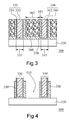
- FIGS. 3-8 illustrate various cross-sectional views of a contact structure 300 of a gate structure during formation of the contact structure 300 according to a first embodiment.
- the contact structure 300 includes a silicon substrate 320 , a first metal gate 330 , a second metal gate 340 , a first sidewall layer 350 , and an oxidation layer 360 .
- a high-K metal gate last process has been completed to form the first metal gate 330 and the second metal gate 340 .
- the first metal gate 330 includes a first metal body 332 and a first spacer 334 for at least partially coating the first metal body 332 .
- the second gate 340 includes a second metal body 342 and a second spacer 344 for at least partially coating the second metal body 342 .
- the first sidewall layer 350 is interposed between the first gate 330 and the second gate 340 .
- a first lateral side (e.g. the right side) of the first metal gate 330 is oppose to a second lateral side (e.g. the left side) of the second metal gate 340 .
- the first sidewall layer 350 is formed using a nitride-based film because of having high selectivity for withstanding etchants used in at least one following etching process.
- the first sidewall layer 350 is formed using a material selected from the group consisting of SiN x , SiO (1-x) N x , SiC (1-x) N x , SiO (1-x-y) C x N y , Ti (1-x) N x , and Al (1-x) N x .
- the material also has a high selectivity for withstanding etchants used in at least one following etching process.
- an average of a thickness 352 of the first sidewall layer 350 may be between about 1 nanometer (nm) and about 5 nm.
- a distance 362 between a first portion (a portion next to the spacer 334 ) of the first metal gate 330 and a second portion (a portion next to the spacer 344 ) of the first sidewall layer 350 may be between about 15 nm and 45 nm.
- a width 335 of the first metal gate 330 is between about 10 nm and about 30 nm
- a width 345 of the second metal gate 340 is between about 10 nm and about 30 nm.
- a first chemical mechanical polishing (CMP) process may be optionally performed to planarize the first metal gate 330 , the second metal gate 340 , and the first sidewall layer 350 .
- CMP chemical mechanical polishing
- the oxidation layer 360 and part of the first sidewall layer 350 underlying the oxidation layer 360 are etched to expose the silicon substrate 320 underlying the oxidation layer 360 .
- a contact profile 410 is thus defined between the first metal gate 330 and the second metal gate 340 in an interposed manner.
- Part of the first sidewall layer 350 that is in direct contact with the first metal gate 330 and the second metal gate 340 may also be slightly etched.
- the oxidation layer 360 and part of the first sidewall layer 350 underlying the oxidation layer 360 may be etched using an isotropic etching process.
- the isotropic etching process is an ion bombardment process.
- a silicide portion 520 is deposited following the contact profile 410 in an exposed portion of the silicon substrate 320 .
- the silicide portion 520 is deposited using a material selected from the group consisting of Ti (1-x) Si x , Co (1-x) Si x , Ni (1-x) Si x , Ti (1-x) Si x Ge, Co (1-x) Si x Ge, and Ni (1-x) Si x Ge.
- a second sidewall layer 630 is substantially formed to cover the first sidewall layer 350 and to at least partially cover the silicide portion 520 .
- the second sidewall layer 630 is formed using a material selected from the group consisting of SiO x , SiO x C (1-x) , SiN x , SiO (1-x) N x , SiC (1-x) N x , SiO (1-x-y) C x N y , Ti (1-x) N x , and Al (1-x) N x .
- an average of a thickness 640 of the second sidewall layer 630 is between about 10 angstrom ( ⁇ ) and about 50 ⁇ .
- a metal glue layer 740 is deposited around the first metal gate 330 and the second metal gate 340 .
- a trench 750 is thus defined above the silicide portion 520 by the metal glue layer 750 .
- a metal plug 760 is then deposited within the trench 750 .
- the metal glue layer 740 is deposited using tungsten. In another example, the metal plug 760 is deposited using tungsten.
- an aspect ratio of the trench 750 may be reduced.
- a second CMP process is performed on the metal plug 760 , the metal glue layer 740 , the first metal gate 330 , the second metal gate 340 , the first sidewall layer 350 , and the second sidewall layer 630 for planarizing the metal plug 760 , the metal glue layer 740 , the first metal gate 330 , the second metal gate 340 , the first sidewall layer 350 , and the second sidewall layer 630 .
- the first sidewall layer 350 and the second sidewall layer 630 are used for separating the first metal gate 330 or the second metal gate 340 from the metal plug 760 for reducing hole and electron scattering.
- a contact area of a bottom of the metal plug 760 will be more accessible in comparison to the contact area at the bottom of the contact layer 210 . Therefore, resistance of the contact area of the metal plug 760 may be easier to control, and fitting a size of the contact area of the metal plug 760 to better critical dimension uniformity (CDU) may be easier.
- CDU critical dimension uniformity
- the silicide portion 520 suffers only minimal damage by the high temperature of the high-K metal gate last process.
- the first sidewall layer is thick enough to separate the first metal gate or the second metal gate from the metal plug for reducing hole and electron scattering, so that the second sidewall layer need not be used.
- FIGS. 9-10 illustrate various cross-sectional views of a contact structure 900 of a gate structure during formation of the contact structure according to the second embodiment.
- the contact structure 900 includes a silicon substrate 960 , a first metal gate 910 , a second metal gate 920 , a first sidewall layer 930 , and a silicide layer 950 .
- the first metal gate 910 includes a first metal body 912 and a first spacer 914 for at least partially coating the first metal body 912 .
- the second gate 920 includes a second metal body 922 and a second spacer 924 for at least partially coating the second metal body 922 .
- a metal glue layer 940 is deposited around the first metal gate 910 and the second metal gate 920 .
- a trench 970 is thus defined above the silicide portion 950 by the metal glue layer 940 .
- a metal plug 980 is then deposited within the trench 970 .
- an aspect ratio of the trench 970 may be reduced.
- a CMP process is performed on the metal plug 980 , the metal glue layer 940 , the first metal gate 910 , the second metal gate 920 , and the first sidewall layer 930 for planarizing metal plug 980 , the metal glue layer 940 , the first metal gate 910 , the second metal gate 920 , and the first sidewall layer 930 .
- the abovementioned advantages of the contact structure 300 may also be taken by the contact structure 900 . Repeated descriptions about advantages of the contact structure 900 are saved for brevity.
- FIG. 11 illustrates a flowchart of a method of forming a contact structure of a contact structure according to the first embodiment.
- the method includes the following stages: Optionally perform a first CMP process on a first metal gate, a second metal gate, and a first sidewall layer ( 1102 ). Etch an oxidation layer and the first sidewall layer disposed between the first metal gate and the second metal gate to expose an underlying silicon substrate ( 1104 ). Deposit a silicide portion defined by a contact profile in the exposed portion of the silicon substrate ( 1106 ). Form a second sidewall layer substantially covering the first sidewall layer and at least partially covering the silicide portion ( 1108 ). Deposit a metal glue layer around the first metal gate and the second metal gate defining a trench above the silicide portion ( 1110 ). Deposit a metal plug within the trench ( 1112 ). Performing a second CMP process on the metal plug, the metal glue layer, the first metal gate, the second metal gate, the first sidewall layer, and the second sidewall layer ( 1114 ).
- FIG. 12 illustrates a flowchart of a method of forming a contact structure of a contact structure according to the second embodiment.
- the method includes the following stages: Optionally perform a first CMP process on a first metal gate, a second metal gate, and a first sidewall layer ( 1202 ). Etch an oxidation layer and the first sidewall layer disposed between the first metal gate and the second metal gate to expose an underlying silicon substrate ( 1204 ). Deposit a silicide portion defined by a contact profile in the exposed portion of the silicon substrate ( 1206 ). Deposit a metal glue layer around the first metal gate and the second metal gate defining a trench above the silicide portion ( 1208 ). Deposit a metal plug within the trench ( 1210 ). Perform a second CMP process on the metal plug, the metal glue layer, the first metal gate, the second metal gate, and the first sidewall layer ( 1212 ).
- This disclosure teaches a method of forming a contact structure of a gate structure.
- an oxidation layer and a first sidewall layer disposed between a first metal gate and a second metal gate are etched to expose an underlying silicon substrate.
- a silicide portion defined by a contact profile in the exposed portion of the silicon substrate is deposited.
- a second sidewall layer substantially covering the first sidewall layer and at least partially covering the silicide portion is formed after the silicide portion is deposited.
- a metal glue layer is deposited around the first metal gate and the second metal gate defining a trench above the silicide portion.
- a metal plug is deposited within the trench.
- This disclosure also teaches a method of forming a contact structure of a gate structure.
- an oxidation layer and a first sidewall layer disposed between a first metal gate and a second metal gate are etched to expose an underlying silicon substrate.
- a silicide portion defined by a contact profile is deposited in the exposed portion of the silicon substrate.
- a metal glue layer is deposited around the first metal gate and the second metal gate defining a trench above the silicide portion.
- a metal plug is deposited within the trench.
- the contact structure includes a silicide portion, a first metal gate, a second metal gate, a first sidewall layer, a metal glue layer, and a metal plug.
- the silicide portion is formed in the silicon substrate.
- the first metal gate is formed above the silicon substrate.
- a second metal gate is formed above the silicon substrate.
- a first sidewall layer at least partially covers a first lateral side of the first metal gate and a second lateral side of the second metal gate.
- the first sidewall layer is interposed between the first metal gate and the second metal gate.
- the first lateral side of the first metal gate is oppose to the second lateral side of the second metal gate.
- a metal glue layer is deposited around the first metal gate and the second metal gate defining a trench above the silicide portion.
- a metal plug is deposited within the trench.
- terms designating relative vertical position may refer to a situation where a device side (or active surface) of a substrate or integrated circuit is the “top” surface of that substrate; the substrate may actually be in any orientation so that a “top” side of a substrate may be lower than the “bottom” side in a standard terrestrial frame of reference and may still fall within the meaning of the term “top.”
- the term “on” as used herein may not indicate that a first layer “on” a second layer is directly on and in immediate contact with the second layer unless such is specifically stated; there may be a third layer or other structure between the first layer and the second layer on the first layer.
- substrate may refer to any construction comprising one or more semiconductive materials, including, but not limited to, bulk semiconductive materials such as a semiconductive wafer (either alone or in assemblies comprising other materials thereon), and semiconductive material layers (either alone or in assemblies comprising other materials).
- semiconductive materials including, but not limited to, bulk semiconductive materials such as a semiconductive wafer (either alone or in assemblies comprising other materials thereon), and semiconductive material layers (either alone or in assemblies comprising other materials).
- the embodiments of a device or article described herein can be manufactured, used, or shipped in a number of positions and orientations. Persons skilled in the art will recognize various equivalent combinations and substitutions for various components shown in the figures.
Abstract
A method of forming a contact structure of a gate structure is provided. In the method, an oxidation layer and a first sidewall layer disposed between a first metal gate and a second metal gate are etched to expose an underlying silicon substrate. A silicide portion defined by a contact profile is deposited in the exposed portion of the silicon substrate. A second sidewall layer substantially covers the first sidewall layer and at least partially covering the silicide portion is formed after depositing the silicide portion. A metal glue layer is deposited around the first metal gate and the second metal gate defining a trench above the silicide portion. A metal plug is deposited within the trench.
Description
This application is a divisional application of U.S. patent application Ser. No. 14/840,099, entitled “Method of Forming Contact Structure of Gate Structure,” filed Aug. 31, 2015, which is a continuation of U.S. patent application Ser. No. 14/157,576, now U.S. Pat. No. 9,123,563, entitled “Method of Forming Contact Structure of Gate Structure,” filed Jan. 17, 2014, both of which are incorporated herein by reference in their entireties.
This disclosure relates to semiconductor technology, and more particularly, a method of forming a contact structure of a gate structure.
In a contact formation process of a gate structure of a MOSFET, a contact structure is patterned by lithography and etching, and a silicide portion is formed via a pattern of the contact structure. However, the small size of the silicide portion may decrease the stability and the capability of the contact structure after formation of the contact structure is complete.
The first gate 151 includes part of the hard mask layer 110, part of the metal gate layer 120, a first left-side spacer 152, and a first right-side spacer 154. The second gate 155 includes part of the hard mask layer 110, part of the metal gate layer 120, a second left-side spacer 156, and a second right-side spacer 158.
Under a self-align contact process, if the hard mask layer 110 is not thick enough, after a gap-filling process for depositing the gap-fill layer 160, heights of the first gate 151 and the second gate 155 may not be high enough; a process for pushing the metal gate layer 120 downwards may not succeed; and the gap-filling process may not succeed. Moreover, using the hard mask layer 110 may raise complexity of forming the contact structure 100, and difficulty of precisely aligning a contact structure for the epitaxial layer 140, which will be formed into a source or a drain.
Before formation of the contact structure 200, a photolithography process and an etching process are performed. A trench holding the contact layer 210 is thus formed between the first gate 222 and the second gate 224. The trench may have a high aspect ratio. While depositing the contact layer 210 within the trench, the high aspect ratio of the trench limits a contact area of a bottom of the contact layer 210. The limited contact area of the bottom of the contact layer 210 also limits an area of the sicilide layer 240.
The small area of the silicide layer 240 also results in large resistance of the silicide layer 240, and operation of the contact structure 200 will be difficult to manipulate due to the large resistance of the silicide layer 240.
If a width of the insulator layer 250 (such as a width 252 or a width 254 shown in FIG. 2 ) is not large enough, the hole and electron scattering between the contact layer 210 and the first gate 222 or the second gate 224 may not be effectively alleviated. However, a large width of the insulator layer 250 also results in a high aspect ratio of the trench holding the contact layer 210 and a small area of the silicide layer 240, and results in an increased size the contact structure 200.
If the area of the silicide layer 240 is limited, i.e. a contact size of the contact structure 200, flexibility of critical dimension uniformity (CDU) of the contact structure 200 may also be restricted.
In one example, the silicide layer 240 may consist essentially of NiSi, and a temperature of forming the silicide layer 240 may be about 400-500 centigrade degrees. However, since formation of the contact structure 200 may experience a high-K metal gate last (HK-last) process, and since a temperature of using the high-K metal gate last process may be about 800-1000 centigrade degrees, the silicide layer 240 may be damaged by the high temperature of the high-K metal gate last process.
In FIG. 3 , the contact structure 300 includes a silicon substrate 320, a first metal gate 330, a second metal gate 340, a first sidewall layer 350, and an oxidation layer 360.
A high-K metal gate last process has been completed to form the first metal gate 330 and the second metal gate 340. The first metal gate 330 includes a first metal body 332 and a first spacer 334 for at least partially coating the first metal body 332. The second gate 340 includes a second metal body 342 and a second spacer 344 for at least partially coating the second metal body 342.
The first sidewall layer 350 is interposed between the first gate 330 and the second gate 340. A first lateral side (e.g. the right side) of the first metal gate 330 is oppose to a second lateral side (e.g. the left side) of the second metal gate 340.
In a first example, the first sidewall layer 350 is formed using a nitride-based film because of having high selectivity for withstanding etchants used in at least one following etching process.
In a second example, the first sidewall layer 350 is formed using a material selected from the group consisting of SiNx, SiO(1-x)Nx, SiC(1-x)Nx, SiO(1-x-y)CxNy, Ti(1-x)Nx, and Al(1-x)Nx. The material also has a high selectivity for withstanding etchants used in at least one following etching process.
In a third example, an average of a thickness 352 of the first sidewall layer 350 may be between about 1 nanometer (nm) and about 5 nm.
In a fourth example, a distance 362 between a first portion (a portion next to the spacer 334) of the first metal gate 330 and a second portion (a portion next to the spacer 344) of the first sidewall layer 350 may be between about 15 nm and 45 nm.
In a fifth example, a width 335 of the first metal gate 330 is between about 10 nm and about 30 nm, and a width 345 of the second metal gate 340 is between about 10 nm and about 30 nm.
In FIG. 3 , a first chemical mechanical polishing (CMP) process may be optionally performed to planarize the first metal gate 330, the second metal gate 340, and the first sidewall layer 350.
In FIG. 4 , the oxidation layer 360 and part of the first sidewall layer 350 underlying the oxidation layer 360 are etched to expose the silicon substrate 320 underlying the oxidation layer 360. A contact profile 410 is thus defined between the first metal gate 330 and the second metal gate 340 in an interposed manner. Part of the first sidewall layer 350 that is in direct contact with the first metal gate 330 and the second metal gate 340 may also be slightly etched.
In one example, the oxidation layer 360 and part of the first sidewall layer 350 underlying the oxidation layer 360 may be etched using an isotropic etching process. In another example, the isotropic etching process is an ion bombardment process.
In FIG. 5 , a silicide portion 520 is deposited following the contact profile 410 in an exposed portion of the silicon substrate 320.
In one example, the silicide portion 520 is deposited using a material selected from the group consisting of Ti(1-x)Six, Co(1-x)Six, Ni(1-x)Six, Ti(1-x)SixGe, Co(1-x)SixGe, and Ni(1-x)SixGe.
In FIG. 6 , a second sidewall layer 630 is substantially formed to cover the first sidewall layer 350 and to at least partially cover the silicide portion 520.
In a first example, the second sidewall layer 630 is formed using a material selected from the group consisting of SiOx, SiOxC(1-x), SiNx, SiO(1-x)Nx, SiC(1-x)Nx, SiO(1-x-y)CxNy, Ti(1-x)Nx, and Al(1-x)Nx.
In a second example, an average of a thickness 640 of the second sidewall layer 630 is between about 10 angstrom (Å) and about 50 Å.
In FIG. 7 , a metal glue layer 740 is deposited around the first metal gate 330 and the second metal gate 340. A trench 750 is thus defined above the silicide portion 520 by the metal glue layer 750. A metal plug 760 is then deposited within the trench 750.
In one example, the metal glue layer 740 is deposited using tungsten. In another example, the metal plug 760 is deposited using tungsten.
In FIG. 7 , because of a tapered structure of the trench 750 formed with the aid of the first sidewall layer 350 and the second sidewall layer 630, an aspect ratio of the trench 750 may be reduced.
In FIG. 8 , a second CMP process is performed on the metal plug 760, the metal glue layer 740, the first metal gate 330, the second metal gate 340, the first sidewall layer 350, and the second sidewall layer 630 for planarizing the metal plug 760, the metal glue layer 740, the first metal gate 330, the second metal gate 340, the first sidewall layer 350, and the second sidewall layer 630.
In the first embodiment, the first sidewall layer 350 and the second sidewall layer 630 are used for separating the first metal gate 330 or the second metal gate 340 from the metal plug 760 for reducing hole and electron scattering. In FIG. 8 since the aspect ratio of the trench 750 is reduced, a contact area of a bottom of the metal plug 760 will be more accessible in comparison to the contact area at the bottom of the contact layer 210. Therefore, resistance of the contact area of the metal plug 760 may be easier to control, and fitting a size of the contact area of the metal plug 760 to better critical dimension uniformity (CDU) may be easier.
In the first embodiment, because a hard mask layer is not used, defects caused by using a hard mask layer are reduced.
In the first embodiment, since the high-K metal gate last process is performed in advance, the silicide portion 520 suffers only minimal damage by the high temperature of the high-K metal gate last process.
In a second embodiment, the first sidewall layer is thick enough to separate the first metal gate or the second metal gate from the metal plug for reducing hole and electron scattering, so that the second sidewall layer need not be used.
Before the formation of the contact structure 900 shown in FIG. 9 , the processes shown in FIGS. 3-5 are performed.
In FIG. 9 , the contact structure 900 includes a silicon substrate 960, a first metal gate 910, a second metal gate 920, a first sidewall layer 930, and a silicide layer 950.
The first metal gate 910 includes a first metal body 912 and a first spacer 914 for at least partially coating the first metal body 912. The second gate 920 includes a second metal body 922 and a second spacer 924 for at least partially coating the second metal body 922.
A metal glue layer 940 is deposited around the first metal gate 910 and the second metal gate 920. A trench 970 is thus defined above the silicide portion 950 by the metal glue layer 940. A metal plug 980 is then deposited within the trench 970.
Similarly, because of a tapered structure of the trench 970 formed with the aid of the first sidewall layer 930, an aspect ratio of the trench 970 may be reduced.
In FIG. 10 , a CMP process is performed on the metal plug 980, the metal glue layer 940, the first metal gate 910, the second metal gate 920, and the first sidewall layer 930 for planarizing metal plug 980, the metal glue layer 940, the first metal gate 910, the second metal gate 920, and the first sidewall layer 930.
In the second embodiment, since the aspect ratio of the trench 970 is reduced, the abovementioned advantages of the contact structure 300 may also be taken by the contact structure 900. Repeated descriptions about advantages of the contact structure 900 are saved for brevity.
In FIG. 11 , the method includes the following stages: Optionally perform a first CMP process on a first metal gate, a second metal gate, and a first sidewall layer (1102). Etch an oxidation layer and the first sidewall layer disposed between the first metal gate and the second metal gate to expose an underlying silicon substrate (1104). Deposit a silicide portion defined by a contact profile in the exposed portion of the silicon substrate (1106). Form a second sidewall layer substantially covering the first sidewall layer and at least partially covering the silicide portion (1108). Deposit a metal glue layer around the first metal gate and the second metal gate defining a trench above the silicide portion (1110). Deposit a metal plug within the trench (1112). Performing a second CMP process on the metal plug, the metal glue layer, the first metal gate, the second metal gate, the first sidewall layer, and the second sidewall layer (1114).
In FIG. 12 , the method includes the following stages: Optionally perform a first CMP process on a first metal gate, a second metal gate, and a first sidewall layer (1202). Etch an oxidation layer and the first sidewall layer disposed between the first metal gate and the second metal gate to expose an underlying silicon substrate (1204). Deposit a silicide portion defined by a contact profile in the exposed portion of the silicon substrate (1206). Deposit a metal glue layer around the first metal gate and the second metal gate defining a trench above the silicide portion (1208). Deposit a metal plug within the trench (1210). Perform a second CMP process on the metal plug, the metal glue layer, the first metal gate, the second metal gate, and the first sidewall layer (1212).
This disclosure teaches a method of forming a contact structure of a gate structure. In this method, an oxidation layer and a first sidewall layer disposed between a first metal gate and a second metal gate are etched to expose an underlying silicon substrate. A silicide portion defined by a contact profile in the exposed portion of the silicon substrate is deposited. A second sidewall layer substantially covering the first sidewall layer and at least partially covering the silicide portion is formed after the silicide portion is deposited. A metal glue layer is deposited around the first metal gate and the second metal gate defining a trench above the silicide portion. A metal plug is deposited within the trench.
This disclosure also teaches a method of forming a contact structure of a gate structure. In the method, an oxidation layer and a first sidewall layer disposed between a first metal gate and a second metal gate are etched to expose an underlying silicon substrate. A silicide portion defined by a contact profile is deposited in the exposed portion of the silicon substrate. A metal glue layer is deposited around the first metal gate and the second metal gate defining a trench above the silicide portion. A metal plug is deposited within the trench.
This disclosure also teaches a contact structure of a gate structure. The contact structure includes a silicide portion, a first metal gate, a second metal gate, a first sidewall layer, a metal glue layer, and a metal plug. The silicide portion is formed in the silicon substrate. The first metal gate is formed above the silicon substrate. A second metal gate is formed above the silicon substrate. A first sidewall layer at least partially covers a first lateral side of the first metal gate and a second lateral side of the second metal gate. The first sidewall layer is interposed between the first metal gate and the second metal gate. The first lateral side of the first metal gate is oppose to the second lateral side of the second metal gate. A metal glue layer is deposited around the first metal gate and the second metal gate defining a trench above the silicide portion. A metal plug is deposited within the trench.
This written description uses examples to disclose embodiments of the disclosure, include the best mode, and also to enable a person of ordinary skill in the art to make and use various embodiments of the disclosure. The patentable scope of the disclosure may include other examples that occur to those of ordinary skill in the art. One of ordinary skill in the relevant art will recognize that the various embodiments may be practiced without one or more of the specific details, or with other replacement and/or additional methods, materials, or components. Well-known structures, materials, or operations may not be shown or described in detail to avoid obscuring aspects of various embodiments of the disclosure. Various embodiments shown in the figures are illustrative example representations and are not necessarily drawn to scale. Particular features, structures, materials, or characteristics may be combined in any suitable manner in one or more embodiments. Various additional layers and/or structures may be included and/or described features may be omitted in other embodiments. Various operations may be described as multiple discrete operations in turn, in a manner that is most helpful in understanding the disclosure. However, the order of description should not be construed as to imply that these operations are necessarily order dependent. In particular, these operations need not be performed in the order of presentation. Operations described herein may be performed in a different order, in series or in parallel, than the described embodiments. Various additional operations may be performed and/or described. Operations may be omitted in additional embodiments.
This written description and the following claims may include terms, such as left, right, top, bottom, over, under, upper, lower, first, second, etc. that are used for descriptive purposes only and are not to be construed as limiting. For example, terms designating relative vertical position may refer to a situation where a device side (or active surface) of a substrate or integrated circuit is the “top” surface of that substrate; the substrate may actually be in any orientation so that a “top” side of a substrate may be lower than the “bottom” side in a standard terrestrial frame of reference and may still fall within the meaning of the term “top.” The term “on” as used herein (including in the claims) may not indicate that a first layer “on” a second layer is directly on and in immediate contact with the second layer unless such is specifically stated; there may be a third layer or other structure between the first layer and the second layer on the first layer. As an example, the structures, layouts, materials, operations, voltage levels, or current levels related to “source” and “drain” described herein (including in the claims) may be interchangeable as a result of transistors with “source” and “drain” being symmetrical devices. The term “substrate” may refer to any construction comprising one or more semiconductive materials, including, but not limited to, bulk semiconductive materials such as a semiconductive wafer (either alone or in assemblies comprising other materials thereon), and semiconductive material layers (either alone or in assemblies comprising other materials). The embodiments of a device or article described herein can be manufactured, used, or shipped in a number of positions and orientations. Persons skilled in the art will recognize various equivalent combinations and substitutions for various components shown in the figures.
Claims (20)
1. A contact structure of a gate structure comprising:
a silicide portion formed in a silicon substrate;
a first metal gate formed above the silicon substrate;
a second metal gate formed above the silicon substrate;
spacer material at least partially covering a first lateral side of the first metal gate and a second lateral side of the second metal gate, the first lateral side of the first metal gate being opposite to the second lateral side of the second metal gate;
a first sidewall layer that (i) substantially covers the spacer material, and (ii) comprises a material that is different than that of the spacer material, wherein the first sidewall layer is interposed between the first metal gate and the second metal gate and is not disposed on top of the silicide portion;
a second sidewall layer substantially covering the first sidewall layer and at least partially covering the silicide portion;
a metal glue layer deposited around the first metal gate and the second metal gate defining a trench above the silicide portion; and
a metal plug deposited within the trench,
wherein a top surface of the first sidewall layer and a top surface of the second sidewall layer are coplanar with a top surface of the first metal gate, a top surface of the second metal gate, and a top surface of the metal plug.
2. The contact structure of claim 1 , wherein the first lateral side of the first metal gate is a right side of the first metal gate, and the second lateral side of the second metal gate is a left side of the second metal gate.
3. The contact structure of claim 1 , wherein the first lateral side of the first metal gate is a left side of the first metal gate, and the second lateral side of the second metal gate is a right side of the second metal gate.
4. The contact structure of claim 1 , wherein a material of the second sidewall layer is selected from the group consisting of SiOx, SiOxC(1-x), SiNx, SiO(1-x)Nx, SiC(1-x)Nx, SiO(1-x-y)CxNy, Ti(1-x)Nx, and Al(1-x)Nx.
5. The contact structure of claim 1 , wherein an average thickness of the second sidewall layer is between about 10 angstrom (Å) and about 50 Å.
6. The contact structure of claim 1 , wherein the first sidewall layer is a nitride-based film.
7. The contact structure of claim 1 , wherein a material of the first sidewall layer is selected from the group consisting of SiNx, SiO(1-x)Nx, SiC(1-x)Nx, SiO(1-x-y) CxNy, Ti(1-x)Nx, and Al(1-x)Nx.
8. The contact structure of claim 1 , wherein an average thickness of the first sidewall layer is between about 1 nanometer (nm) and about 5 nm.
9. The contact structure of claim 1 , wherein a distance between a first portion of the first sidewall layer at least partially covering the first lateral side of the first metal gate and a second portion of the first sidewall layer at least partially covering the second lateral side of the second metal gate is between about 15 nm and about 45 nm.
10. The contact structure of claim 1 , wherein a material of the silicide portion is selected from the group consisting of Ti(1-x)Six, Co(1-x)Six, Ni(1-x)Six, Ti(1-x) SixGe, Co(1-x)SixGe, and Ni(1-x)SixGe.
11. The contact structure of claim 1 , wherein a width of the first metal gate is between about 10 nm and about 30 nm, and a width of the second metal gate is between about 10 nm and about 30 nm.
12. A contact structure of a gate structure comprising:
a silicide portion formed in a substrate;
a first gate formed above the substrate;
a second gate formed above the substrate;
spacer material at least partially covering a first side of the first gate and a second side of the second gate, the first side of the first gate being opposite to the second side of the second gate;
a first sidewall layer that (i) substantially covers the spacer material, and (ii) comprises a material that is different than that of the spacer material, the first sidewall layer being interposed between the first gate and the second gate and not disposed on top of the silicide portion;
a second sidewall layer substantially covering the first sidewall layer and at least partially covering the silicide portion;
a glue layer formed around the first gate and the second gate and defining a trench above the silicide portion; and
a plug disposed within the trench,
wherein a top surface of the first sidewall layer and a top surface of the second sidewall layer are coplanar with a top surface of the first gate, a top surface of the second gate, and a top surface of the plug.
13. The contact structure of claim 12 , wherein the second sidewall layer is substantially covered by the glue layer.
14. The contact structure of claim 13 , wherein a material of the second sidewall layer is selected from the group consisting of SiOx, SiOxC(1-x), SiNx, SiO(1-x)Nx, SiC(1-x)Nx, SiO(1-x-y)CxNy, Ti(1-x)Nx, and Al(1-x)Nx.
15. The contact structure of claim 13 , wherein an average thickness of the second sidewall layer is between about 10 angstrom (Å) and about 50 Å.
16. The contact structure of claim 12 , wherein the first sidewall layer is a nitride-based film.
17. The contact structure of claim 12 , wherein a material of the first sidewall layer is selected from the group consisting of SiNx, SiO(1-x)Nx, SiC(1-x)Nx, SiO(1-x-y) CxNy, Ti(1-x)Nx, and Al(1-x)Nx.
18. The contact structure of claim 12 , wherein an average thickness of the first sidewall layer is between about 1 nanometer (nm) and about 5 nm.
19. A contact structure of a gate structure comprising:
a silicide portion formed in a substrate;
a first gate formed above the substrate;
a second gate formed above the substrate;
spacer material at least partially covering a first lateral side of the first gate and a second lateral side of the second gate;
a first sidewall layer formed above the substrate and substantially covering the spacer material, wherein the first sidewall layer is not disposed on top of the silicide portion;
a second sidewall layer substantially covering the first sidewall layer and at least partially covering the silicide portion;
a glue layer disposed around the first gate and the second gate that defines a trench above the silicide portion; and
a plug disposed within the trench
wherein a top surface of the first sidewall layer and a top surface of the second sidewall layer are coplanar with a top surface of the first gate, a top surface of the second gate, and a top surface of the plug.
20. The contact structure of claim 1 , wherein the second sidewall layer is not formed above the first sidewall layer.
Priority Applications (1)
| Application Number | Priority Date | Filing Date | Title |
|---|---|---|---|
| US15/384,446 US10276437B2 (en) | 2014-01-17 | 2016-12-20 | Contact structure of gate structure |
Applications Claiming Priority (3)
| Application Number | Priority Date | Filing Date | Title |
|---|---|---|---|
| US14/157,576 US9123563B2 (en) | 2014-01-17 | 2014-01-17 | Method of forming contact structure of gate structure |
| US14/840,099 US9536754B2 (en) | 2014-01-17 | 2015-08-31 | Method of forming contact structure of gate structure |
| US15/384,446 US10276437B2 (en) | 2014-01-17 | 2016-12-20 | Contact structure of gate structure |
Related Parent Applications (1)
| Application Number | Title | Priority Date | Filing Date |
|---|---|---|---|
| US14/840,099 Division US9536754B2 (en) | 2014-01-17 | 2015-08-31 | Method of forming contact structure of gate structure |
Publications (2)
| Publication Number | Publication Date |
|---|---|
| US20170103918A1 US20170103918A1 (en) | 2017-04-13 |
| US10276437B2 true US10276437B2 (en) | 2019-04-30 |
Family
ID=53497600
Family Applications (3)
| Application Number | Title | Priority Date | Filing Date |
|---|---|---|---|
| US14/157,576 Expired - Fee Related US9123563B2 (en) | 2014-01-17 | 2014-01-17 | Method of forming contact structure of gate structure |
| US14/840,099 Active US9536754B2 (en) | 2014-01-17 | 2015-08-31 | Method of forming contact structure of gate structure |
| US15/384,446 Active US10276437B2 (en) | 2014-01-17 | 2016-12-20 | Contact structure of gate structure |
Family Applications Before (2)
| Application Number | Title | Priority Date | Filing Date |
|---|---|---|---|
| US14/157,576 Expired - Fee Related US9123563B2 (en) | 2014-01-17 | 2014-01-17 | Method of forming contact structure of gate structure |
| US14/840,099 Active US9536754B2 (en) | 2014-01-17 | 2015-08-31 | Method of forming contact structure of gate structure |
Country Status (3)
| Country | Link |
|---|---|
| US (3) | US9123563B2 (en) |
| DE (1) | DE102014019205B4 (en) |
| TW (1) | TWI559383B (en) |
Families Citing this family (4)
| Publication number | Priority date | Publication date | Assignee | Title |
|---|---|---|---|---|
| US9123563B2 (en) | 2014-01-17 | 2015-09-01 | Taiwan Semiconductor Manufacturing Company Limited | Method of forming contact structure of gate structure |
| CN105575946A (en) | 2014-10-16 | 2016-05-11 | 中芯国际集成电路制造(上海)有限公司 | Semiconductor structure and formation method thereof |
| US10090249B2 (en) * | 2015-12-17 | 2018-10-02 | Taiwan Semiconductor Manufacturing Company, Ltd. | Semiconductor structure and manufacturing method thereof |
| EP3920212A1 (en) * | 2016-12-30 | 2021-12-08 | INTEL Corporation | Contact architecture for capacitance reduction and satisfactory contact resistance |
Citations (14)
| Publication number | Priority date | Publication date | Assignee | Title |
|---|---|---|---|---|
| US20030227046A1 (en) | 2002-03-18 | 2003-12-11 | Takashi Ando | Semiconductor device and method of manufacturing the same |
| TW200511399A (en) | 2003-09-04 | 2005-03-16 | Promos Technologies Inc | Method of forming a gate and method of forming a contact window |
| US20070040196A1 (en) | 2005-08-17 | 2007-02-22 | Fujitsu Limited | Semiconductor device and manufacturing method thereof, and thin film device |
| US20080054328A1 (en) * | 2006-08-29 | 2008-03-06 | Fujitsu Limited | Semiconductor device and method of manufacturing the same |
| US20080061331A1 (en) * | 2006-09-12 | 2008-03-13 | Fujitsu Limited | Semiconductor device and manufacturing method thereof |
| US20080191253A1 (en) * | 2005-09-30 | 2008-08-14 | Fujitsu Limited | Semiconductor device and method for manufacturing the same |
| US20090026514A1 (en) * | 2006-03-30 | 2009-01-29 | Fujitsu Limited | Semiconductor device and manufacturing method thereof |
| TW201023344A (en) | 2008-12-02 | 2010-06-16 | United Microelectronics Corp | Contact efuse structure, method of making a contact efuse device containing the same, and method of making a read only memory containing the same |
| US20110272753A1 (en) | 2009-01-15 | 2011-11-10 | Renesas Electronics Corporation | Semiconductor device and method of manufacturing the same |
| US20120032299A1 (en) * | 2010-08-06 | 2012-02-09 | Fujitsu Semiconductor Limited | Semiconductor device and method of manufacturing the same |
| US20130277756A1 (en) * | 2012-04-18 | 2013-10-24 | Fujitsu Semiconductor Limited | Semiconductor device and method of manufacturing the same |
| US20140273386A1 (en) * | 2013-03-14 | 2014-09-18 | United Microelectronics Corp. | Method of forming metal silicide layer |
| US20140327141A1 (en) * | 2012-04-13 | 2014-11-06 | Taiwan Semiconductor Manufacturing Company, Ltd. | Copper interconnect structure and method for forming the same |
| US9123563B2 (en) | 2014-01-17 | 2015-09-01 | Taiwan Semiconductor Manufacturing Company Limited | Method of forming contact structure of gate structure |
Family Cites Families (8)
| Publication number | Priority date | Publication date | Assignee | Title |
|---|---|---|---|---|
| US7563701B2 (en) | 2005-03-31 | 2009-07-21 | Intel Corporation | Self-aligned contacts for transistors |
| US20090051034A1 (en) | 2007-08-20 | 2009-02-26 | Taiwan Semiconductor Manufacturing Co., Ltd. | Semiconductor device and method for the same |
| US8803245B2 (en) | 2008-06-30 | 2014-08-12 | Mcafee, Inc. | Method of forming stacked trench contacts and structures formed thereby |
| DE102010063780A1 (en) | 2010-12-21 | 2012-06-21 | Globalfoundries Dresden Module One Limited Liability Company & Co. Kg | Semiconductor device having a contact structure with a lower parasitic capacitance |
| US8614123B2 (en) | 2011-11-28 | 2013-12-24 | Globalfoundries Inc. | Method of forming a semiconductor device by using sacrificial gate electrodes and sacrificial self-aligned contact structures |
| US8741718B2 (en) | 2012-01-17 | 2014-06-03 | International Business Machines Corporation | Local interconnects compatible with replacement gate structures |
| US8741723B2 (en) | 2012-04-25 | 2014-06-03 | Globalfoundries Inc. | Methods of forming self-aligned contacts for a semiconductor device |
| US8524592B1 (en) | 2012-08-13 | 2013-09-03 | Globalfoundries Inc. | Methods of forming semiconductor devices with self-aligned contacts and low-k spacers and the resulting devices |
-
2014
- 2014-01-17 US US14/157,576 patent/US9123563B2/en not_active Expired - Fee Related
- 2014-12-19 DE DE102014019205.9A patent/DE102014019205B4/en active Active
- 2014-12-30 TW TW103146196A patent/TWI559383B/en active
-
2015
- 2015-08-31 US US14/840,099 patent/US9536754B2/en active Active
-
2016
- 2016-12-20 US US15/384,446 patent/US10276437B2/en active Active
Patent Citations (15)
| Publication number | Priority date | Publication date | Assignee | Title |
|---|---|---|---|---|
| US20030227046A1 (en) | 2002-03-18 | 2003-12-11 | Takashi Ando | Semiconductor device and method of manufacturing the same |
| US7221015B2 (en) | 2002-03-18 | 2007-05-22 | Fujitsu Limited | Semiconductor device and method of manufacturing the same |
| TW200511399A (en) | 2003-09-04 | 2005-03-16 | Promos Technologies Inc | Method of forming a gate and method of forming a contact window |
| US20070040196A1 (en) | 2005-08-17 | 2007-02-22 | Fujitsu Limited | Semiconductor device and manufacturing method thereof, and thin film device |
| US20080191253A1 (en) * | 2005-09-30 | 2008-08-14 | Fujitsu Limited | Semiconductor device and method for manufacturing the same |
| US20090026514A1 (en) * | 2006-03-30 | 2009-01-29 | Fujitsu Limited | Semiconductor device and manufacturing method thereof |
| US20080054328A1 (en) * | 2006-08-29 | 2008-03-06 | Fujitsu Limited | Semiconductor device and method of manufacturing the same |
| US20080061331A1 (en) * | 2006-09-12 | 2008-03-13 | Fujitsu Limited | Semiconductor device and manufacturing method thereof |
| TW201023344A (en) | 2008-12-02 | 2010-06-16 | United Microelectronics Corp | Contact efuse structure, method of making a contact efuse device containing the same, and method of making a read only memory containing the same |
| US20110272753A1 (en) | 2009-01-15 | 2011-11-10 | Renesas Electronics Corporation | Semiconductor device and method of manufacturing the same |
| US20120032299A1 (en) * | 2010-08-06 | 2012-02-09 | Fujitsu Semiconductor Limited | Semiconductor device and method of manufacturing the same |
| US20140327141A1 (en) * | 2012-04-13 | 2014-11-06 | Taiwan Semiconductor Manufacturing Company, Ltd. | Copper interconnect structure and method for forming the same |
| US20130277756A1 (en) * | 2012-04-18 | 2013-10-24 | Fujitsu Semiconductor Limited | Semiconductor device and method of manufacturing the same |
| US20140273386A1 (en) * | 2013-03-14 | 2014-09-18 | United Microelectronics Corp. | Method of forming metal silicide layer |
| US9123563B2 (en) | 2014-01-17 | 2015-09-01 | Taiwan Semiconductor Manufacturing Company Limited | Method of forming contact structure of gate structure |
Non-Patent Citations (1)
| Title |
|---|
| Taiwan Notice of Allowance; Application No. 103146196; dated Aug. 19, 2016. |
Also Published As
| Publication number | Publication date |
|---|---|
| US9536754B2 (en) | 2017-01-03 |
| DE102014019205B4 (en) | 2024-01-25 |
| TWI559383B (en) | 2016-11-21 |
| US20150380270A1 (en) | 2015-12-31 |
| US20150206872A1 (en) | 2015-07-23 |
| TW201539553A (en) | 2015-10-16 |
| US9123563B2 (en) | 2015-09-01 |
| US20170103918A1 (en) | 2017-04-13 |
| DE102014019205A1 (en) | 2015-07-23 |
Similar Documents
| Publication | Publication Date | Title |
|---|---|---|
| US11846871B2 (en) | Device with a recessed gate electrode that has high thickness uniformity | |
| US9385193B2 (en) | FINFET transistor structure and method for making the same | |
| US10276437B2 (en) | Contact structure of gate structure | |
| US8765491B2 (en) | Shallow trench isolation recess repair using spacer formation process | |
| US9853128B2 (en) | Devices and methods of forming unmerged epitaxy for FinFET device | |
| TW201517177A (en) | Trench sidewall protection for selective epitaxial semiconductor material formation | |
| US9570319B2 (en) | Method of manufacturing a semiconductor device | |
| US20170309725A1 (en) | Semiconductor device and formation thereof | |
| TWI609457B (en) | Method of forming contact hole and semiconductor structure with contact plug | |
| US20230187542A1 (en) | Multi-layer dielectric refill for profile control in semiconductor devices | |
| US9349634B2 (en) | Semiconductor arrangement and formation thereof | |
| US10256311B2 (en) | Fin field effect transistor (FinFET) | |
| US9991169B2 (en) | Semiconductor device and formation thereof | |
| US11127837B2 (en) | Method of forming MOSFET structure | |
| US9911825B2 (en) | Integrated circuits with spacer chamfering and methods of spacer chamfering | |
| TWI689040B (en) | Semiconductor device and method of fabricating the same | |
| US20170222049A1 (en) | Vertical transistor and the fabrication method | |
| US20170162720A1 (en) | Gate Structure | |
| US20150200136A1 (en) | Semiconductor device, method for forming contact and method for etching continuous recess |
Legal Events
| Date | Code | Title | Description |
|---|---|---|---|
| AS | Assignment |
Owner name: RAKA CORPORATION, OHIO Free format text: ASSIGNMENT OF ASSIGNORS INTEREST;ASSIGNORS:STEFFES, ERIC;DUPUIS, CLAUDE;REEL/FRAME:040746/0657 Effective date: 20161220 |
|
| STPP | Information on status: patent application and granting procedure in general |
Free format text: PUBLICATIONS -- ISSUE FEE PAYMENT VERIFIED |
|
| STCF | Information on status: patent grant |
Free format text: PATENTED CASE |
|
| MAFP | Maintenance fee payment |
Free format text: PAYMENT OF MAINTENANCE FEE, 4TH YEAR, LARGE ENTITY (ORIGINAL EVENT CODE: M1551); ENTITY STATUS OF PATENT OWNER: LARGE ENTITY Year of fee payment: 4 |