US10243344B2 - Semiconductor device - Google Patents
Semiconductor device Download PDFInfo
- Publication number
- US10243344B2 US10243344B2 US15/278,179 US201615278179A US10243344B2 US 10243344 B2 US10243344 B2 US 10243344B2 US 201615278179 A US201615278179 A US 201615278179A US 10243344 B2 US10243344 B2 US 10243344B2
- Authority
- US
- United States
- Prior art keywords
- voltage
- overcurrent protection
- generate
- circuit
- output transistor
- Prior art date
- Legal status (The legal status is an assumption and is not a legal conclusion. Google has not performed a legal analysis and makes no representation as to the accuracy of the status listed.)
- Active, expires
Links
Images


Classifications
-
- H—ELECTRICITY
- H02—GENERATION; CONVERSION OR DISTRIBUTION OF ELECTRIC POWER
- H02H—EMERGENCY PROTECTIVE CIRCUIT ARRANGEMENTS
- H02H3/00—Emergency protective circuit arrangements for automatic disconnection directly responsive to an undesired change from normal electric working condition with or without subsequent reconnection ; integrated protection
- H02H3/08—Emergency protective circuit arrangements for automatic disconnection directly responsive to an undesired change from normal electric working condition with or without subsequent reconnection ; integrated protection responsive to excess current
- H02H3/093—Emergency protective circuit arrangements for automatic disconnection directly responsive to an undesired change from normal electric working condition with or without subsequent reconnection ; integrated protection responsive to excess current with timing means
-
- H—ELECTRICITY
- H02—GENERATION; CONVERSION OR DISTRIBUTION OF ELECTRIC POWER
- H02M—APPARATUS FOR CONVERSION BETWEEN AC AND AC, BETWEEN AC AND DC, OR BETWEEN DC AND DC, AND FOR USE WITH MAINS OR SIMILAR POWER SUPPLY SYSTEMS; CONVERSION OF DC OR AC INPUT POWER INTO SURGE OUTPUT POWER; CONTROL OR REGULATION THEREOF
- H02M1/00—Details of apparatus for conversion
- H02M1/32—Means for protecting converters other than automatic disconnection
-
- H—ELECTRICITY
- H02—GENERATION; CONVERSION OR DISTRIBUTION OF ELECTRIC POWER
- H02H—EMERGENCY PROTECTIVE CIRCUIT ARRANGEMENTS
- H02H3/00—Emergency protective circuit arrangements for automatic disconnection directly responsive to an undesired change from normal electric working condition with or without subsequent reconnection ; integrated protection
- H02H3/02—Details
- H02H3/025—Disconnection after limiting, e.g. when limiting is not sufficient or for facilitating disconnection
-
- H—ELECTRICITY
- H02—GENERATION; CONVERSION OR DISTRIBUTION OF ELECTRIC POWER
- H02H—EMERGENCY PROTECTIVE CIRCUIT ARRANGEMENTS
- H02H3/00—Emergency protective circuit arrangements for automatic disconnection directly responsive to an undesired change from normal electric working condition with or without subsequent reconnection ; integrated protection
- H02H3/08—Emergency protective circuit arrangements for automatic disconnection directly responsive to an undesired change from normal electric working condition with or without subsequent reconnection ; integrated protection responsive to excess current
- H02H3/087—Emergency protective circuit arrangements for automatic disconnection directly responsive to an undesired change from normal electric working condition with or without subsequent reconnection ; integrated protection responsive to excess current for DC applications
-
- H—ELECTRICITY
- H02—GENERATION; CONVERSION OR DISTRIBUTION OF ELECTRIC POWER
- H02H—EMERGENCY PROTECTIVE CIRCUIT ARRANGEMENTS
- H02H7/00—Emergency protective circuit arrangements specially adapted for specific types of electric machines or apparatus or for sectionalised protection of cable or line systems, and effecting automatic switching in the event of an undesired change from normal working conditions
- H02H7/10—Emergency protective circuit arrangements specially adapted for specific types of electric machines or apparatus or for sectionalised protection of cable or line systems, and effecting automatic switching in the event of an undesired change from normal working conditions for converters; for rectifiers
- H02H7/12—Emergency protective circuit arrangements specially adapted for specific types of electric machines or apparatus or for sectionalised protection of cable or line systems, and effecting automatic switching in the event of an undesired change from normal working conditions for converters; for rectifiers for static converters or rectifiers
- H02H7/1213—Emergency protective circuit arrangements specially adapted for specific types of electric machines or apparatus or for sectionalised protection of cable or line systems, and effecting automatic switching in the event of an undesired change from normal working conditions for converters; for rectifiers for static converters or rectifiers for DC-DC converters
-
- H—ELECTRICITY
- H02—GENERATION; CONVERSION OR DISTRIBUTION OF ELECTRIC POWER
- H02H—EMERGENCY PROTECTIVE CIRCUIT ARRANGEMENTS
- H02H7/00—Emergency protective circuit arrangements specially adapted for specific types of electric machines or apparatus or for sectionalised protection of cable or line systems, and effecting automatic switching in the event of an undesired change from normal working conditions
- H02H7/10—Emergency protective circuit arrangements specially adapted for specific types of electric machines or apparatus or for sectionalised protection of cable or line systems, and effecting automatic switching in the event of an undesired change from normal working conditions for converters; for rectifiers
- H02H7/12—Emergency protective circuit arrangements specially adapted for specific types of electric machines or apparatus or for sectionalised protection of cable or line systems, and effecting automatic switching in the event of an undesired change from normal working conditions for converters; for rectifiers for static converters or rectifiers
- H02H7/122—Emergency protective circuit arrangements specially adapted for specific types of electric machines or apparatus or for sectionalised protection of cable or line systems, and effecting automatic switching in the event of an undesired change from normal working conditions for converters; for rectifiers for static converters or rectifiers for inverters, i.e. DC/AC converters
-
- H—ELECTRICITY
- H02—GENERATION; CONVERSION OR DISTRIBUTION OF ELECTRIC POWER
- H02H—EMERGENCY PROTECTIVE CIRCUIT ARRANGEMENTS
- H02H9/00—Emergency protective circuit arrangements for limiting excess current or voltage without disconnection
- H02H9/02—Emergency protective circuit arrangements for limiting excess current or voltage without disconnection responsive to excess current
-
- H—ELECTRICITY
- H02—GENERATION; CONVERSION OR DISTRIBUTION OF ELECTRIC POWER
- H02M—APPARATUS FOR CONVERSION BETWEEN AC AND AC, BETWEEN AC AND DC, OR BETWEEN DC AND DC, AND FOR USE WITH MAINS OR SIMILAR POWER SUPPLY SYSTEMS; CONVERSION OF DC OR AC INPUT POWER INTO SURGE OUTPUT POWER; CONTROL OR REGULATION THEREOF
- H02M3/00—Conversion of DC power input into DC power output
- H02M3/02—Conversion of DC power input into DC power output without intermediate conversion into AC
- H02M3/04—Conversion of DC power input into DC power output without intermediate conversion into AC by static converters
- H02M3/10—Conversion of DC power input into DC power output without intermediate conversion into AC by static converters using discharge tubes with control electrode or semiconductor devices with control electrode
- H02M3/145—Conversion of DC power input into DC power output without intermediate conversion into AC by static converters using discharge tubes with control electrode or semiconductor devices with control electrode using devices of a triode or transistor type requiring continuous application of a control signal
- H02M3/155—Conversion of DC power input into DC power output without intermediate conversion into AC by static converters using discharge tubes with control electrode or semiconductor devices with control electrode using devices of a triode or transistor type requiring continuous application of a control signal using semiconductor devices only
-
- H—ELECTRICITY
- H02—GENERATION; CONVERSION OR DISTRIBUTION OF ELECTRIC POWER
- H02M—APPARATUS FOR CONVERSION BETWEEN AC AND AC, BETWEEN AC AND DC, OR BETWEEN DC AND DC, AND FOR USE WITH MAINS OR SIMILAR POWER SUPPLY SYSTEMS; CONVERSION OF DC OR AC INPUT POWER INTO SURGE OUTPUT POWER; CONTROL OR REGULATION THEREOF
- H02M7/00—Conversion of AC power input into DC power output; Conversion of DC power input into AC power output
- H02M7/02—Conversion of AC power input into DC power output without possibility of reversal
- H02M7/04—Conversion of AC power input into DC power output without possibility of reversal by static converters
- H02M7/12—Conversion of AC power input into DC power output without possibility of reversal by static converters using discharge tubes with control electrode or semiconductor devices with control electrode
- H02M7/21—Conversion of AC power input into DC power output without possibility of reversal by static converters using discharge tubes with control electrode or semiconductor devices with control electrode using devices of a triode or transistor type requiring continuous application of a control signal
- H02M7/217—Conversion of AC power input into DC power output without possibility of reversal by static converters using discharge tubes with control electrode or semiconductor devices with control electrode using devices of a triode or transistor type requiring continuous application of a control signal using semiconductor devices only
Definitions
- the present invention relates to a semiconductor device including an overcurrent protection circuit.
- Patent Document 1 PCT International Publication No. 2012/157242 filed by this applicant (hereinafter referred to as Patent Document 1) discloses a non-insulation step-down switching regulator having an overcurrent protection function, in which coil current is always monitored using an externally connected sense resistor disposed immediately close to the coil, so that an output transistor is forcibly turned off continuously in a period while the coil current exceeds a predetermined threshold current.
- Patent Document 1 needs the externally connected sense resistor, and hence there is a problem that a substrate area and cost are increased.
- an object of the invention disclosed in this specification is to provide an overcurrent protection circuit that can perform an appropriate overcurrent protection operation without necessity of an externally connected sense resistor.
- a semiconductor device disclosed in this specification includes an integration of a first external terminal to which a DC input voltage is input, a second external terminal to which a rectifying and smoothing circuit is externally connected, an output transistor connected between the first external terminal and the second external terminal, a control circuit arranged to turn on and off the output transistor so that a desired DC output voltage can be obtained from the rectifying and smoothing circuit, a current detection circuit arranged to generate a sense voltage corresponding to an on-current of the output transistor, and an overcurrent protection circuit arranged to monitor the sense voltage so as to perform an overcurrent protection operation.
- the overcurrent protection circuit performs a first overcurrent protection operation of a pulse-by-pulse method when detecting that the sense voltage exceeds a first threshold value voltage, and performs a second overcurrent protection operation of a timer latch method when detecting that the sense voltage continues to increase though the first overcurrent protection operation is being performed.
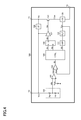
- FIG. 1 is a circuit block diagram illustrating an overall structure of an electronic apparatus.
- FIG. 2 is a current path diagram during an on period of an output transistor.
- FIG. 3 is a current path diagram during an off period of the output transistor.
- FIG. 4 is a block diagram illustrating a basic structure of a semiconductor device.
- FIG. 5 is a block diagram illustrating a first embodiment of an overcurrent protection circuit.
- FIG. 6 is a timing chart illustrating a first overcurrent protection operation of a pulse-by-pulse method.
- FIG. 7 is a timing chart illustrating an overcurrent protection operation of a first embodiment.
- FIG. 8 is a block diagram illustrating a second embodiment of the overcurrent protection circuit.
- FIG. 9 is a timing chart illustrating an overcurrent protection operation of a second embodiment.
- FIG. 10 is an external view of an air conditioner.
- FIG. 1 is a circuit block diagram illustrating an overall structure of an electronic apparatus.
- An electronic apparatus X of this structural example includes a power supply device 1 that receives supply of an AC input voltage Vac from an AC power source Y so as to generate a desired DC output voltage Vout, and a load 2 that receives supply of the DC output voltage Vout so as to operate.
- the power supply device 1 includes a filter 10 , an AC/DC converter 20 , and a DC/DC converter 30 .
- the filter 10 eliminates noise and surge superimposed on the AC input voltage Vac.
- the filter 10 includes an X capacitor, a common mode filter, a fuse element, and the like.
- the AC/DC converter 20 generates a DC input voltage Vin from the AC input voltage Vac that is input via the filter 10 .
- the AC/DC converter 20 includes a diode bridge DB for full wave rectification and a capacitor C 0 for output smoothing.
- the DC/DC converter 30 is a non-insulation step-down switching regulator that steps down the DC input voltage Vin so as to generate the desired DC output voltage Vout, and supplies the same to the load 2 .
- the DC/DC converter 30 includes a semiconductor device 100 and discrete components (a coil L 1 , diodes D 1 and D 2 , and capacitors C 1 and C 2 ) that are externally connected to the semiconductor device 100 .
- the semiconductor device 100 is a main controller (so-called a switching control IC) of the DC/DC converter 30 , and has external terminals T 1 to T 3 as means for establishing electric connection with the outside of the device.
- the external terminal T 1 (DRAIN pin) corresponds to an input terminal of the DC input voltage Vin.
- the external terminal T 2 (GND_IC pin) corresponds to an output terminal of a switched voltage Vsw.
- the external terminal T 3 (VCC pin) corresponds to an input terminal of a power supply voltage Vcc.
- a first terminal of the coil L 1 and a cathode of the diode D 1 are both connected to the external terminal T 2 .
- a second terminal of the coil L 1 and a first terminal of the capacitor C 1 are both connected to an output terminal of the output voltage Vout.
- An anode of the diode D 1 and a second terminal of the capacitor C 1 are both connected to a ground terminal.
- These discrete components (the coil L 1 , the diode D 1 , and the capacitor C 1 ) function as a rectifying and smoothing circuit that rectifies and smoothes the switched voltage Vsw so as to generate the desired DC output voltage Vout.
- a synchronous rectifying transistor may be integrated in the semiconductor device 100 .
- a cathode of the diode D 2 and a first terminal of the capacitor C 2 are both connected to the external terminal T 3 .
- a second terminal of the capacitor C 2 is connected to the external terminal T 2 .
- An anode of the diode D 2 is connected to the output terminal of the output voltage Vout.
- an output transistor 101 is disposed between the external terminal T 1 and the external terminal T 2 , and a current path of the coil current IL is switched in accordance with an on/off state of the output transistor 101 .
- FIG. 2 is a current path diagram during an on period of the output transistor 101 .
- an on-current Ion flows in the path from the capacitor C 0 to the output transistor 101 , to the coil L 1 , and to the capacitor C 1 , as illustrated by a broken line arrow.
- FIG. 3 is a current path diagram during an off period of the output transistor 101 .
- an off-current Ioff flows in the path from the diode D 1 to the coil L 1 , and to the capacitor C 1 , as illustrated by a broken line arrow.
- FIG. 4 is a block diagram illustrating a basic structure of the semiconductor device 100 .
- the semiconductor device 100 of this structural example includes an integration of the output transistor 101 , a feedback voltage generation circuit 102 , an error amplifier circuit 103 , a comparator circuit 104 , a control circuit 105 , an RS flip-flop circuit 106 , a driving circuit 107 , a start circuit 108 , a current detection circuit 109 , a filter circuit 110 , and an overcurrent protection circuit 111 .
- various circuit blocks an internal power supply circuit, a decrease voltage protection circuit, a temperature protection circuit, an overvoltage protection circuit, and the like
- the output transistor 101 is a switching element connected between the external terminal T 1 and the external terminal T 2 .
- an N-channel metal oxide semiconductor (MOS) field effect transistor is used as the output transistor 101 .
- a drain of the output transistor 101 is connected to the external terminal T 1 .
- a source of the output transistor 101 is connected to the external terminal T 2 .
- a gate of the output transistor 101 is connected to an output terminal of the driving circuit 107 (i.e. an output terminal of a gate signal S 4 ).
- the output transistor 101 is turned on when the gate signal S 4 is at a high level and is turned off when the gate signal S 4 is at a low level. Note that it is possible to use a P-channel MOS field effect transistor as the output transistor 101 .
- the error amplifier circuit 103 generates an error voltage Verr corresponding to a difference between a reference voltage Vref input to a non-inverting input terminal (+) and the feedback voltage Vfb input to an inverting input terminal ( ⁇ ) (corresponding to a divided voltage of the output voltage Vout).
- the error voltage Verr increases when the feedback voltage Vfb is lower than the reference voltage Vref and decreases when the feedback voltage Vfb is higher than the reference voltage Vref.
- the comparator circuit 104 compares the error voltage Verr input to the non-inverting input terminal (+) with a sense voltage Vcs input to the inverting input terminal ( ⁇ ) so as to generate a pulse width modulation signal S 0 .
- the pulse width modulation signal S 0 becomes the high level when the error voltage Verr is higher than the sense voltage Vcs and becomes the low level when the error voltage Verr is lower than the sense voltage Vcs.
- the sense voltage Vcs is directly input to the comparator circuit 104 , but as another structure, it is possible to input to the comparator circuit 104 a sum voltage of the sense voltage Vcs plus a slope voltage having a triangular waveform or a sawtooth waveform, for example.
- current mode control is not necessary, it is possible to input only the slope voltage described above to the comparator circuit 104 .
- the control circuit 105 generates an ON signal S 1 and an OFF signal S 2 according to the pulse width modulation signal S 0 so that the desired DC output voltage Vout can be obtained from the rectifying and smoothing circuit (L 1 , D 1 , C 1 ) described above.
- the ON signal S 1 is a reference clock signal having a predetermined switching frequency fsw.
- the OFF signal S 2 is a one-shot signal generated by a trigger of a pulse edge of the pulse width modulation signal S 0 .
- the method of driving the output transistor 101 by the control circuit 105 is not limited to the pulse width modulation method, but any method such as a pulse frequency modulation method may be adopted.
- the RS flip-flop circuit 106 receives inputs of the ON signal S 1 and the OFF signal S 2 so as to generate an ON/OFF control signal S 3 . More specifically, the RS flip-flop circuit 106 sets the ON/OFF control signal S 3 to the high level at a pulse edge of the ON signal S 1 , and resets the ON/OFF control signal S 3 to the low level at a pulse edge of the OFF signal S 2 .
- the driving circuit 107 receives supply of the power supply voltage Vcc so as to operate, and enhances current ability of the ON/OFF control signal S 3 so as to generate the gate signal S 4 .
- the ON/OFF control signal S 3 is at the high level, the gate signal S 4 becomes the high level, and the output transistor 101 is turned on.
- the ON/OFF control signal S 3 is at the low level, the gate signal S 4 becomes the low level, and the output transistor 101 is turned off.
- the start circuit 108 makes a short circuit between the external terminal T 1 and the external terminal T 3 so as to increase the power supply voltage Vcc using the DC input voltage Vin. Accordingly, even if a sufficient power supply voltage Vcc cannot be generated from the output voltage Vout, there is no problem in the on/off control of the output transistor 101 .
- the current detection circuit 109 uses a wiring resistance of the current path in which the on-current Ion flows, an on-resistance of the output transistor 101 , or an on-resistance of a transistor for monitoring current connected in parallel to the output transistor 101 , as a sense resistor, and hence generates the sense voltage Vcs corresponding to the on-current Ion.
- the sense voltage Vcs becomes higher as the on-current Ion is larger, and becomes lower as the on-current Ion is smaller.
- the current detection circuit 109 is disposed at the position.
- the position of the current detection circuit 109 is not limited to this.
- the current detection circuit 109 is disposed not at the source side but at the drain side of the output transistor 101 .
- the current detection circuit 109 is connected in parallel to the output transistor 101 .
- the filter circuit 110 is connected between the current detection circuit 109 and the overcurrent protection circuit 111 so as to eliminate noise components (switching noise and the like) superimposed on the sense voltage Vcs.
- the overcurrent protection circuit 111 monitors the sense voltage Vcs input via the filter circuit 110 and generates an overcurrent protection signal S 5 , so as to perform an overcurrent protection operation. More specifically, the overcurrent protection circuit 111 generates the overcurrent protection signal S 5 , so as to perform a first overcurrent protection operation of a pulse-by-pulse method when detecting that the sense voltage Vcs exceeds a first threshold value voltage Vth 1 , and to perform a second overcurrent protection operation of a timer latch method when detecting that the sense voltage Vcs continues to increase though the first overcurrent protection operation is being performed.
- a structure and an operation of the overcurrent protection circuit 111 are described in detail.
- FIG. 5 is a block diagram illustrating a first embodiment of the overcurrent protection circuit 111 .
- the overcurrent protection circuit 111 of this embodiment includes comparators 111 a 1 and 111 a 2 , a counter 111 b , and a timer 111 c , and monitors the sense voltage Vcs so as to generate the overcurrent protection signal S 5 .
- the overcurrent protection signal S 5 includes a first overcurrent protection signal S 5 X for the first overcurrent protection operation and a second overcurrent protection signal S 5 Y for the second overcurrent protection operation.
- the comparator 111 a 1 compares the sense voltage Vcs input to the non-inverting input terminal (+) with the first threshold value voltage Vth 1 input to the inverting input terminal ( ⁇ ) so as to generate a first comparison signal Sa 1 .
- the first comparison signal Sa 1 becomes the low level when the sense voltage Vcs is lower than the first threshold value voltage Vth 1 , and becomes the high level when the sense voltage Vcs is higher than the first threshold value voltage Vth 1 .
- a relationship between the sense voltage Vcs and the first threshold value voltage Vth 1 can be read as a relationship between the on-current Ion and a first threshold current Ith 1 .
- the first comparison signal Sa 1 becomes the low level when the on-current Ion is smaller than the first threshold current Ith 1 , and becomes the high level when the on-current Ion is larger than the first threshold current Ith 1 . Further, the first comparison signal Sa 1 is output to the control circuit 105 as the first overcurrent protection signal S 5 X.
- the comparator 111 a 2 compares the sense voltage Vcs input to the non-inverting input terminal (+) with a second threshold value voltage Vth 2 (>Vth 1 ) input to the inverting input terminal ( ⁇ ) so as to generate a second comparison signal Sa 2 .
- the second comparison signal Sa 2 becomes the low level when the sense voltage Vcs is lower than the second threshold value voltage Vth 2 , and becomes the high level when the sense voltage Vcs is higher than the second threshold value voltage Vth 2 .
- a relationship between the sense voltage Vcs and the second threshold value voltage Vth 2 can be read as a relationship between the on-current Ion and a second threshold current Ith 2 (>Ith 1 ).
- the second comparison signal Sa 2 becomes the low level when the on-current Ion is smaller than the second threshold current Ith 2 , and becomes the high level when the on-current Ion is larger than the second threshold current Ith 2 .
- the counter 111 b generates a one-shot signal Sb when detecting pulses of the second comparison signal Sa 2 continuously for a plurality of periods.
- the timer 111 c generates a timer signal Sc to be the high level for a predetermined time T by a trigger of a pulse edge of the one-shot signal Sb.
- the timer 111 c may be either a digital timer or an analog timer. Note that the timer signal Sc is output to the control circuit 105 as the second overcurrent protection signal S 5 Y.
- the control circuit 105 When the on-current Ion becomes larger than the first threshold current Ith 1 so that the first overcurrent protection signal S 5 X is raised to the high level, the control circuit 105 forcibly turns off the output transistor 101 until the on timing of the next period. In this way, in the first overcurrent protection operation of the pulse-by-pulse method, the forced stop and self-reset of the switching operation are repeated every period while the on-current Ion exceeds the first threshold current Ith 1 . Accordingly, even if an overcurrent is temporarily detected due to a load fluctuation or the like, the switching operation is not forced to stop continuously, and hence the output voltage Vout can be stably generated.
- the control circuit 105 When the on-current Ion becomes larger than the first threshold current Ith 1 so that the first overcurrent protection signal S 5 X is raised to the high level, the control circuit 105 forcibly turns off the output transistor 101 until the on timing of the next period. In this way, when it is determined that the on-current Ion exceeds the first threshold current Ith 1 , the first overcurrent protection operation of the pulse-by-pulse method is performed as described above with reference to FIG. 6 .
- the on-current Ion continues to increase though the first overcurrent protection operation is being performed, and if the on-current Ion becomes higher than the second threshold current Ith 2 as a result, a pulse is generated in the second comparison signal Sa 2 . Further, if the increase of the on-current Ion continues for a plurality of periods after that, and if a plurality of (two in the illustrated example) pulses are generated continuously in the second comparison signal Sa 2 , a pulse is generated in the one-shot signal Sb.
- the second overcurrent protection signal S 5 Y (i.e. the timer signal Sc) is raised to the high level by a trigger of the pulse of the one-shot signal Sb, and then is maintained at the high level for the predetermined time T.
- the control circuit 105 When the second overcurrent protection signal S 5 Y is raised to the high level, the control circuit 105 forcibly turns off the output transistor 101 during the high level period of the second overcurrent protection signal S 5 Y (i.e. the predetermined time T). In this way, if the on-current Ion continues to increase though the first overcurrent protection operation of the pulse-by-pulse method is being performed, it is switched to the second overcurrent protection operation of the timer latch method, and the output transistor 101 is forcibly turned off for a plurality of periods. Accordingly, even if the output terminal of the output voltage Vout is short-circuited to the ground, for example, appropriate overcurrent protection can be performed.
- FIG. 8 is a block diagram illustrating a second embodiment of the overcurrent protection circuit 111 .
- the overcurrent protection circuit 111 of this embodiment has a structure based on the first embodiment ( FIG. 5 ), in which a comparator 111 a 3 is added, and further the counter 111 b is replaced with a logic unit 111 b 2 . Accordingly, the same structural element as in the first embodiment is denoted by the same reference numeral as in FIG. 5 so that overlapping description is omitted. In the following description, characteristic parts of the second embodiment are mainly described.
- the comparator 111 a 3 compares the sense voltage Vcs input to the non-inverting input terminal (+) with a third threshold value voltage Vth 3 input to the inverting input terminal ( ⁇ ) (here, Vth 1 ⁇ Vth 3 ⁇ Vth 2 holds), so as to generate a third comparison signal Sa 3 .
- the third comparison signal Sa 3 becomes the low level when the sense voltage Vcs is lower than the third threshold value voltage Vth 3 , and becomes the high level when the sense voltage Vcs is higher than the third threshold value voltage Vth 3 .
- a relationship between the sense voltage Vcs and the third threshold value voltage Vth 3 can be read as a relationship between the on-current Ion and a third threshold current Ith 3 (here, Ith 1 ⁇ Ith 3 ⁇ Ith 2 holds).
- the third comparison signal Sa 3 becomes the low level when the on-current Ion is smaller than the third threshold current Ith 3 , and becomes the high level when the on-current Ion is larger than the third threshold current Ith 3 .
- the logic unit 111 b 2 generates the one-shot signal Sb when detecting a pulse of the third comparison signal Sa 3 and then detecting a pulse of the second comparison signal Sa 2 in the next period.
- the control circuit 105 When the on-current Ion becomes larger than the first threshold current Ith 1 so that the first overcurrent protection signal S 5 X is raised to the high level, the control circuit 105 forcibly turned off the output transistor 101 until the on timing of the next period. In this way, when it is determined that the on-current Ion exceeds the first threshold current Ith 1 , the first overcurrent protection operation of the pulse-by-pulse method is performed, in the same manner as in the first embodiment ( FIG. 7 ) described above.
- the logic unit 111 b 2 generates a pulse in the one-shot signal Sb when detecting that the comparison signals Sa 2 and Sa 3 are switched from the low level and the high level to the high level and the high level, respectively.
- the second overcurrent protection signal S 5 Y (i.e. the timer signal Sc) is raised to the high level by a trigger of the pulse of the one-shot signal Sb, and then is maintained at the high level for the predetermined time T.
- the control circuit 105 When the second overcurrent protection signal S 5 Y is raised to the high level, the control circuit 105 forcibly turns off the output transistor 101 during the high level period of the second overcurrent protection signal S 5 Y (i.e. the predetermined time T). In this way, if the on-current Ion continues to increase though the first overcurrent protection operation of the pulse-by-pulse method is being performed, it is switched to the second overcurrent protection operation of the timer latch method, and the output transistor 101 is forcibly turned off for a plurality of periods, in the same manner as in the first embodiment ( FIG. 7 ) described above. Accordingly, even if the output terminal of the output voltage Vout is short-circuited to the ground, for example, appropriate overcurrent protection can be performed.
- FIG. 10 is an external view of an air conditioner X 1 .
- the air conditioner X 1 is an example of the electronic apparatus X including the power supply device 1 .
- the power supply device 1 can be appropriately mounted in any electronic apparatus other than this.
- the present invention can be applied to power supply devices mounted in various electronic apparatuses (such as an air conditioner, a vacuum cleaner, a refrigerator, and a wash machine).
- various electronic apparatuses such as an air conditioner, a vacuum cleaner, a refrigerator, and a wash machine.
Landscapes
- Engineering & Computer Science (AREA)
- Power Engineering (AREA)
- Dc-Dc Converters (AREA)
Abstract
A semiconductor device includes an integration of a first external terminal to which a DC input voltage is input, a second external terminal to which a rectifying and smoothing circuit is externally connected, an output transistor connected between the first external terminal and the second external terminal, a control circuit arranged to turn on and off the output transistor so that a desired DC output voltage can be obtained from the rectifying and smoothing circuit, a current detection circuit arranged to generate a sense voltage corresponding to an on-current of the output transistor, and an overcurrent protection circuit arranged to monitor the sense voltage so as to perform an overcurrent protection operation. The overcurrent protection circuit performs a first overcurrent protection operation of a pulse-by-pulse method when detecting that the sense voltage exceeds a first threshold value voltage, and performs a second overcurrent protection operation of a timer latch method when detecting that the sense voltage continues to increase though the first overcurrent protection operation is being performed.
Description
This application claims priority based on Japanese Patent Applications No. 2015-190702 filed on Sep. 29, 2015, the contents of which are hereby incorporated by reference.
Field of the Invention
The present invention relates to a semiconductor device including an overcurrent protection circuit.
Description of Related Art
PCT International Publication No. 2012/157242 filed by this applicant (hereinafter referred to as Patent Document 1) discloses a non-insulation step-down switching regulator having an overcurrent protection function, in which coil current is always monitored using an externally connected sense resistor disposed immediately close to the coil, so that an output transistor is forcibly turned off continuously in a period while the coil current exceeds a predetermined threshold current.
However, the conventional technique of Patent Document 1 needs the externally connected sense resistor, and hence there is a problem that a substrate area and cost are increased.
In view of the above-mentioned problem found by the inventor, an object of the invention disclosed in this specification is to provide an overcurrent protection circuit that can perform an appropriate overcurrent protection operation without necessity of an externally connected sense resistor.
A semiconductor device disclosed in this specification includes an integration of a first external terminal to which a DC input voltage is input, a second external terminal to which a rectifying and smoothing circuit is externally connected, an output transistor connected between the first external terminal and the second external terminal, a control circuit arranged to turn on and off the output transistor so that a desired DC output voltage can be obtained from the rectifying and smoothing circuit, a current detection circuit arranged to generate a sense voltage corresponding to an on-current of the output transistor, and an overcurrent protection circuit arranged to monitor the sense voltage so as to perform an overcurrent protection operation. The overcurrent protection circuit performs a first overcurrent protection operation of a pulse-by-pulse method when detecting that the sense voltage exceeds a first threshold value voltage, and performs a second overcurrent protection operation of a timer latch method when detecting that the sense voltage continues to increase though the first overcurrent protection operation is being performed.
Note that other features, elements, steps, advantages, and characteristics of the present invention will become more apparent from the description of the best mode embodiment given below and the related attached drawings.
Continuously, with reference to FIG. 1 , the power supply device 1 is described. The power supply device 1 includes a filter 10, an AC/DC converter 20, and a DC/DC converter 30.
The filter 10 eliminates noise and surge superimposed on the AC input voltage Vac. The filter 10 includes an X capacitor, a common mode filter, a fuse element, and the like.
The AC/DC converter 20 generates a DC input voltage Vin from the AC input voltage Vac that is input via the filter 10. The AC/DC converter 20 includes a diode bridge DB for full wave rectification and a capacitor C0 for output smoothing.
The DC/DC converter 30 is a non-insulation step-down switching regulator that steps down the DC input voltage Vin so as to generate the desired DC output voltage Vout, and supplies the same to the load 2.
Continuously, with reference to FIG. 1 , the DC/DC converter 30 is described. The DC/DC converter 30 includes a semiconductor device 100 and discrete components (a coil L1, diodes D1 and D2, and capacitors C1 and C2) that are externally connected to the semiconductor device 100.
The semiconductor device 100 is a main controller (so-called a switching control IC) of the DC/DC converter 30, and has external terminals T1 to T3 as means for establishing electric connection with the outside of the device. The external terminal T1 (DRAIN pin) corresponds to an input terminal of the DC input voltage Vin. The external terminal T2 (GND_IC pin) corresponds to an output terminal of a switched voltage Vsw. The external terminal T3 (VCC pin) corresponds to an input terminal of a power supply voltage Vcc.
A first terminal of the coil L1 and a cathode of the diode D1 are both connected to the external terminal T2. A second terminal of the coil L1 and a first terminal of the capacitor C1 are both connected to an output terminal of the output voltage Vout. An anode of the diode D1 and a second terminal of the capacitor C1 are both connected to a ground terminal. These discrete components (the coil L1, the diode D1, and the capacitor C1) function as a rectifying and smoothing circuit that rectifies and smoothes the switched voltage Vsw so as to generate the desired DC output voltage Vout. Further, instead of the diode D1, a synchronous rectifying transistor may be integrated in the semiconductor device 100.
A cathode of the diode D2 and a first terminal of the capacitor C2 are both connected to the external terminal T3. A second terminal of the capacitor C2 is connected to the external terminal T2. An anode of the diode D2 is connected to the output terminal of the output voltage Vout. These discrete components (the diode D2 and the capacitor C2) function as a power supply voltage generation circuit that rectifies and smoothes the output voltage Vout so as to generate the power supply voltage Vcc of the semiconductor device 100.
Further, inside the semiconductor device 100, an output transistor 101 is disposed between the external terminal T1 and the external terminal T2, and a current path of the coil current IL is switched in accordance with an on/off state of the output transistor 101.
The output transistor 101 is a switching element connected between the external terminal T1 and the external terminal T2. In the example illustrated in this diagram, an N-channel metal oxide semiconductor (MOS) field effect transistor is used as the output transistor 101. A drain of the output transistor 101 is connected to the external terminal T1. A source of the output transistor 101 is connected to the external terminal T2. A gate of the output transistor 101 is connected to an output terminal of the driving circuit 107 (i.e. an output terminal of a gate signal S4). The output transistor 101 is turned on when the gate signal S4 is at a high level and is turned off when the gate signal S4 is at a low level. Note that it is possible to use a P-channel MOS field effect transistor as the output transistor 101.
The feedback voltage generation circuit 102 includes resistors Ra and Rb connected in series between the external terminal T3 and the ground terminal, and the power supply voltage Vcc (nearly equal to the output voltage Vout) is divided at a predetermined division ratio α (=Rb/(Ra+Rb)), so that a feedback voltage Vfb is output from a connection node between the resistor Ra and the resistor Rb. Further, if the power supply voltage Vcc is within an input dynamic range of the error amplifier circuit 103, the feedback voltage generation circuit 102 can be eliminated so that the power supply voltage Vcc is directly input to the error amplifier circuit 103.
The error amplifier circuit 103 generates an error voltage Verr corresponding to a difference between a reference voltage Vref input to a non-inverting input terminal (+) and the feedback voltage Vfb input to an inverting input terminal (−) (corresponding to a divided voltage of the output voltage Vout). The error voltage Verr increases when the feedback voltage Vfb is lower than the reference voltage Vref and decreases when the feedback voltage Vfb is higher than the reference voltage Vref.
The comparator circuit 104 compares the error voltage Verr input to the non-inverting input terminal (+) with a sense voltage Vcs input to the inverting input terminal (−) so as to generate a pulse width modulation signal S0. The pulse width modulation signal S0 becomes the high level when the error voltage Verr is higher than the sense voltage Vcs and becomes the low level when the error voltage Verr is lower than the sense voltage Vcs. Further, in the example of this diagram, the sense voltage Vcs is directly input to the comparator circuit 104, but as another structure, it is possible to input to the comparator circuit 104 a sum voltage of the sense voltage Vcs plus a slope voltage having a triangular waveform or a sawtooth waveform, for example. In addition, if current mode control is not necessary, it is possible to input only the slope voltage described above to the comparator circuit 104.
The control circuit 105 generates an ON signal S1 and an OFF signal S2 according to the pulse width modulation signal S0 so that the desired DC output voltage Vout can be obtained from the rectifying and smoothing circuit (L1, D1, C1) described above. The ON signal S1 is a reference clock signal having a predetermined switching frequency fsw. The OFF signal S2 is a one-shot signal generated by a trigger of a pulse edge of the pulse width modulation signal S0. However, the method of driving the output transistor 101 by the control circuit 105 is not limited to the pulse width modulation method, but any method such as a pulse frequency modulation method may be adopted.
The RS flip-flop circuit 106 receives inputs of the ON signal S1 and the OFF signal S2 so as to generate an ON/OFF control signal S3. More specifically, the RS flip-flop circuit 106 sets the ON/OFF control signal S3 to the high level at a pulse edge of the ON signal S1, and resets the ON/OFF control signal S3 to the low level at a pulse edge of the OFF signal S2.
The driving circuit 107 receives supply of the power supply voltage Vcc so as to operate, and enhances current ability of the ON/OFF control signal S3 so as to generate the gate signal S4. When the ON/OFF control signal S3 is at the high level, the gate signal S4 becomes the high level, and the output transistor 101 is turned on. On the other hand, when the ON/OFF control signal S3 is at the low level, the gate signal S4 becomes the low level, and the output transistor 101 is turned off.
When the DC/DC converter 30 is started, the start circuit 108 makes a short circuit between the external terminal T1 and the external terminal T3 so as to increase the power supply voltage Vcc using the DC input voltage Vin. Accordingly, even if a sufficient power supply voltage Vcc cannot be generated from the output voltage Vout, there is no problem in the on/off control of the output transistor 101.
The current detection circuit 109 uses a wiring resistance of the current path in which the on-current Ion flows, an on-resistance of the output transistor 101, or an on-resistance of a transistor for monitoring current connected in parallel to the output transistor 101, as a sense resistor, and hence generates the sense voltage Vcs corresponding to the on-current Ion. In other words, the sense voltage Vcs becomes higher as the on-current Ion is larger, and becomes lower as the on-current Ion is smaller.
Further, in this diagram, there is illustrated an example of using a resistance component of a metal wiring between the source of the output transistor 101 and the external terminal T2, in which the current detection circuit 109 is disposed at the position. However, the position of the current detection circuit 109 is not limited to this. For example, when using a resistance component of a metal wiring between the external terminal T1 and the drain of the output transistor 101, the current detection circuit 109 is disposed not at the source side but at the drain side of the output transistor 101. In addition, when using an on-resistance of the output transistor 101, the current detection circuit 109 is connected in parallel to the output transistor 101.
The filter circuit 110 is connected between the current detection circuit 109 and the overcurrent protection circuit 111 so as to eliminate noise components (switching noise and the like) superimposed on the sense voltage Vcs.
The overcurrent protection circuit 111 monitors the sense voltage Vcs input via the filter circuit 110 and generates an overcurrent protection signal S5, so as to perform an overcurrent protection operation. More specifically, the overcurrent protection circuit 111 generates the overcurrent protection signal S5, so as to perform a first overcurrent protection operation of a pulse-by-pulse method when detecting that the sense voltage Vcs exceeds a first threshold value voltage Vth1, and to perform a second overcurrent protection operation of a timer latch method when detecting that the sense voltage Vcs continues to increase though the first overcurrent protection operation is being performed. In the following description, a structure and an operation of the overcurrent protection circuit 111 are described in detail.
The comparator 111 a 1 compares the sense voltage Vcs input to the non-inverting input terminal (+) with the first threshold value voltage Vth1 input to the inverting input terminal (−) so as to generate a first comparison signal Sa1. The first comparison signal Sa1 becomes the low level when the sense voltage Vcs is lower than the first threshold value voltage Vth1, and becomes the high level when the sense voltage Vcs is higher than the first threshold value voltage Vth1. A relationship between the sense voltage Vcs and the first threshold value voltage Vth1 can be read as a relationship between the on-current Ion and a first threshold current Ith1. In other words, the first comparison signal Sa1 becomes the low level when the on-current Ion is smaller than the first threshold current Ith1, and becomes the high level when the on-current Ion is larger than the first threshold current Ith1. Further, the first comparison signal Sa1 is output to the control circuit 105 as the first overcurrent protection signal S5X.
The comparator 111 a 2 compares the sense voltage Vcs input to the non-inverting input terminal (+) with a second threshold value voltage Vth2 (>Vth1) input to the inverting input terminal (−) so as to generate a second comparison signal Sa2. The second comparison signal Sa2 becomes the low level when the sense voltage Vcs is lower than the second threshold value voltage Vth2, and becomes the high level when the sense voltage Vcs is higher than the second threshold value voltage Vth2. A relationship between the sense voltage Vcs and the second threshold value voltage Vth2 can be read as a relationship between the on-current Ion and a second threshold current Ith2 (>Ith1). In other words, the second comparison signal Sa2 becomes the low level when the on-current Ion is smaller than the second threshold current Ith2, and becomes the high level when the on-current Ion is larger than the second threshold current Ith2.
The counter 111 b generates a one-shot signal Sb when detecting pulses of the second comparison signal Sa2 continuously for a plurality of periods.
The timer 111 c generates a timer signal Sc to be the high level for a predetermined time T by a trigger of a pulse edge of the one-shot signal Sb. The timer 111 c may be either a digital timer or an analog timer. Note that the timer signal Sc is output to the control circuit 105 as the second overcurrent protection signal S5Y.
First, prior to detailed description of the overcurrent protection operation of the first embodiment, there is described an outline and a problem of the first overcurrent protection operation of the pulse-by-pulse method using the first overcurrent protection signal S5X with reference to FIG. 6 . FIG. 6 is a timing chart illustrating the first overcurrent protection operation, in which the on-current Ion, the off-current Ioff, the coil current IL (=Ion+Ioff), and the first comparison signal Sa1 (i.e. the first overcurrent protection signal S5X) are shown.
When the on-current Ion becomes larger than the first threshold current Ith1 so that the first overcurrent protection signal S5X is raised to the high level, the control circuit 105 forcibly turns off the output transistor 101 until the on timing of the next period. In this way, in the first overcurrent protection operation of the pulse-by-pulse method, the forced stop and self-reset of the switching operation are repeated every period while the on-current Ion exceeds the first threshold current Ith1. Accordingly, even if an overcurrent is temporarily detected due to a load fluctuation or the like, the switching operation is not forced to stop continuously, and hence the output voltage Vout can be stably generated.
However, if the output terminal of the output voltage Vout is short-circuited to the ground (to the ground terminal or a low potential terminal equivalent to the ground terminal) via a low impedance path, for example, a decrease amount ΔIL of the coil current IL (determined corresponding to Vout/L) during the forced off period of the output transistor 101 is small. Therefore sufficient overcurrent protection cannot be performed, and the coil current IL continues to increase as illustrated in this chart. Consequently, it is necessary to use a large current capacity element as the coil L1, which causes a problem of cost increase.
Further, as described above in Description of Related Art, if the externally connected sense resistor is disposed immediately close to the coil L1, not only the on-current Ion but also the off-current Ioff can be monitored, and hence more appropriate overcurrent protection can be performed. However, in order to adopt this structure, it is necessary to add the externally connected sense resistor, and hence there is a problem that a substrate area and cost are increased.
Next, with reference to FIG. 7 , the overcurrent protection operation of the first embodiment is described in detail. FIG. 7 is a timing chart illustrating the overcurrent protection operation of the first embodiment, in which the on-current Ion, the off-current Ioff, the coil current IL (=Ion+Ioff), the first comparison signal Sa1 (i.e. the first overcurrent protection signal S5X), the second comparison signal Sa2, the one-shot signal Sb, and the timer signal Sc (i.e. the second overcurrent protection signal S5) are shown. Further in this chart, broken lines indicate the behavior when only the first overcurrent protection operation of the pulse-by-pulse method is performed (the behavior illustrated in FIG. 6 ) for comparison and reference.
When the on-current Ion becomes larger than the first threshold current Ith1 so that the first overcurrent protection signal S5X is raised to the high level, the control circuit 105 forcibly turns off the output transistor 101 until the on timing of the next period. In this way, when it is determined that the on-current Ion exceeds the first threshold current Ith1, the first overcurrent protection operation of the pulse-by-pulse method is performed as described above with reference to FIG. 6 .
On the other hand, if the on-current Ion continues to increase though the first overcurrent protection operation is being performed, and if the on-current Ion becomes higher than the second threshold current Ith2 as a result, a pulse is generated in the second comparison signal Sa2. Further, if the increase of the on-current Ion continues for a plurality of periods after that, and if a plurality of (two in the illustrated example) pulses are generated continuously in the second comparison signal Sa2, a pulse is generated in the one-shot signal Sb.
In this case, the second overcurrent protection signal S5Y (i.e. the timer signal Sc) is raised to the high level by a trigger of the pulse of the one-shot signal Sb, and then is maintained at the high level for the predetermined time T. Note that the predetermined time T is longer than a switching period (=1/fsw).
When the second overcurrent protection signal S5Y is raised to the high level, the control circuit 105 forcibly turns off the output transistor 101 during the high level period of the second overcurrent protection signal S5Y (i.e. the predetermined time T). In this way, if the on-current Ion continues to increase though the first overcurrent protection operation of the pulse-by-pulse method is being performed, it is switched to the second overcurrent protection operation of the timer latch method, and the output transistor 101 is forcibly turned off for a plurality of periods. Accordingly, even if the output terminal of the output voltage Vout is short-circuited to the ground, for example, appropriate overcurrent protection can be performed.
The comparator 111 a 3 compares the sense voltage Vcs input to the non-inverting input terminal (+) with a third threshold value voltage Vth3 input to the inverting input terminal (−) (here, Vth1<Vth3<Vth2 holds), so as to generate a third comparison signal Sa3. The third comparison signal Sa3 becomes the low level when the sense voltage Vcs is lower than the third threshold value voltage Vth3, and becomes the high level when the sense voltage Vcs is higher than the third threshold value voltage Vth3. A relationship between the sense voltage Vcs and the third threshold value voltage Vth3 can be read as a relationship between the on-current Ion and a third threshold current Ith3 (here, Ith1<Ith3<Ith2 holds). In other words, the third comparison signal Sa3 becomes the low level when the on-current Ion is smaller than the third threshold current Ith3, and becomes the high level when the on-current Ion is larger than the third threshold current Ith3.
The logic unit 111 b 2 generates the one-shot signal Sb when detecting a pulse of the third comparison signal Sa3 and then detecting a pulse of the second comparison signal Sa2 in the next period.
When the on-current Ion becomes larger than the first threshold current Ith1 so that the first overcurrent protection signal S5X is raised to the high level, the control circuit 105 forcibly turned off the output transistor 101 until the on timing of the next period. In this way, when it is determined that the on-current Ion exceeds the first threshold current Ith1, the first overcurrent protection operation of the pulse-by-pulse method is performed, in the same manner as in the first embodiment (FIG. 7 ) described above.
On the other hand, if the on-current Ion continues to increase though the first overcurrent protection operation is being performed, and if the on-current Ion becomes higher than the third threshold current Ith3 as a result, a pulse is generated in the third comparison signal Sa3. Further, if the increase of the on-current Ion continues, and if a pulse of the second comparison signal Sa2 is generated in the next period, a pulse is generated in the one-shot signal Sb. In other words, the logic unit 111 b 2 generates a pulse in the one-shot signal Sb when detecting that the comparison signals Sa2 and Sa3 are switched from the low level and the high level to the high level and the high level, respectively.
In this case, the second overcurrent protection signal S5Y (i.e. the timer signal Sc) is raised to the high level by a trigger of the pulse of the one-shot signal Sb, and then is maintained at the high level for the predetermined time T. Note that the predetermined time T is longer than a switching period (=1/fsw) as described above.
When the second overcurrent protection signal S5Y is raised to the high level, the control circuit 105 forcibly turns off the output transistor 101 during the high level period of the second overcurrent protection signal S5Y (i.e. the predetermined time T). In this way, if the on-current Ion continues to increase though the first overcurrent protection operation of the pulse-by-pulse method is being performed, it is switched to the second overcurrent protection operation of the timer latch method, and the output transistor 101 is forcibly turned off for a plurality of periods, in the same manner as in the first embodiment (FIG. 7 ) described above. Accordingly, even if the output terminal of the output voltage Vout is short-circuited to the ground, for example, appropriate overcurrent protection can be performed.
Note that the various technical features disclosed in this specification can be variously modified within the scope without deviating from the spirit of the technical invention, other than the embodiments described above. In other words, the embodiments described above are merely examples in every aspect and should not be interpreted as limitations. The technical scope of the present invention is defined not by the above description of the embodiments but by the claims, and should be understood to include all modifications within the meaning and range equivalent to the scope of the claims.
The present invention can be applied to power supply devices mounted in various electronic apparatuses (such as an air conditioner, a vacuum cleaner, a refrigerator, and a wash machine).
Claims (14)
1. A semiconductor device comprising an integration of:
a first external terminal to which a DC input voltage is input;
a second external terminal to which a rectifying and smoothing circuit is externally connected;
an output transistor connected between the first external terminal and the second external terminal;
a control circuit arranged to turn on and off the output transistor so that a desired DC output voltage can be obtained from the rectifying and smoothing circuit;
a current detection circuit arranged to generate a sense voltage corresponding to an on-current of the output transistor; and
an overcurrent protection circuit arranged to monitor the sense voltage so as to perform an overcurrent protection operation, wherein
the overcurrent protection circuit performs a first overcurrent protection operation of a pulse-by-pulse method when detecting that the sense voltage exceeds a first threshold value voltage, and performs a second overcurrent protection operation of a timer latch method when detecting that the sense voltage continues to increase though the first overcurrent protection operation is being performed, wherein
the overcurrent protection circuit includes a first comparator arranged to compare the sense voltage with the first threshold value voltage so as to generate a first comparison signal, and
the control circuit forcibly turns off the output transistor until an on timing of a next period so that the first overcurrent protection operation is performed according to the first comparison signal, wherein the overcurrent protection circuit includes
a second comparator arranged to compare the sense voltage with a second threshold value voltage higher than the first threshold value voltage so as to generate a second comparison signal,
a counter arranged to generate a one-shot signal when a pulse of the second comparison signal is detected continuously for a plurality of periods, and
a timer arranged to generate a timer signal for a predetermined time by a trigger of the one-shot signal, wherein
the control circuit forcibly turns off the output transistor for the predetermined time so that the second overcurrent protection operation is performed according to the timer signal.
2. The semiconductor device according to claim 1 , further comprising an integrated filter circuit connected between the current detection circuit and the overcurrent protection circuit.
3. The semiconductor device according to claim 1 , wherein the current detection circuit generates the sense voltage from the on-current using one of a wiring resistance of a current path in which the on-current flows, an on-resistance of the output transistor, and an on-resistance of a transistor for monitoring current connected in parallel to the output transistor.
4. A DC/DC converter comprising:
a semiconductor device according to claim 1 ; and
a rectifying and smoothing circuit externally connected to the semiconductor device so as to generate a desired DC output voltage.
5. The DC/DC converter according to claim 4 , further comprising a power supply voltage generation circuit externally connected to the semiconductor device so as to generate a power supply voltage of the semiconductor device from the DC output voltage.
6. A power supply device comprising:
an AC/DC converter arranged to generate a DC input voltage from an AC input voltage; and
a DC/DC converter according to claim 4 arranged to generate a desired DC output voltage from the DC input voltage.
7. An electronic apparatus comprising:
a power supply device according to claim 6 arranged to generate a desired DC output voltage from a AC input voltage; and
a load arranged to receive supply of the DC output voltage so as to operate.
8. A semiconductor device comprising an integration of:
a first external terminal to which a DC input voltage is input;
a second external terminal to which a rectifying and smoothing circuit is externally connected;
an output transistor connected between the first external terminal and the second external terminal;
a control circuit arranged to turn on and off the output transistor so that a desired DC output voltage can be obtained from the rectifying and smoothing circuit;
a current detection circuit arranged to generate a sense voltage corresponding to an on-current of the output transistor; and
an overcurrent protection circuit arranged to monitor the sense voltage so as to perform an overcurrent protection operation, wherein
the overcurrent protection circuit performs a first overcurrent protection operation of a pulse-by-pulse method when detecting that the sense voltage exceeds a first threshold value voltage, and performs a second overcurrent protection operation of a timer latch method when detecting that the sense voltage continues to increase though the first overcurrent protection operation is being performed, wherein
the overcurrent protection circuit includes a first comparator arranged to compare the sense voltage with the first threshold value voltage so as to generate a first comparison signal, and
the control circuit forcibly turns off the output transistor until an on timing of a next period so that the first overcurrent protection operation is performed according to the first comparison signal, wherein the overcurrent protection circuit includes
a second comparator arranged to compare the sense voltage with a second threshold value voltage higher than the first threshold value voltage so as to generate a second comparison signal,
a third comparator arranged to compare the sense voltage with a third threshold value voltage higher than the first threshold value voltage and lower than the second threshold value voltage, so as to generate a third comparison signal,
a logic unit arranged to generate a one-shot signal when a pulse of the third comparison signal is detected and then in the next period a pulse of the second comparison signal is detected, and
a timer arranged to generate a timer signal for a predetermined time by a trigger of the one-shot signal, wherein
the control circuit forcibly turns off the output transistor for the predetermined time so that the second overcurrent protection operation is performed according to the timer signal.
9. The semiconductor device according to claim 8 , further comprising an integrated filter circuit connected between the current detection circuit and the overcurrent protection circuit.
10. The semiconductor device according to claim 8 , wherein the current detection circuit generates the sense voltage from the on-current using one of a wiring resistance of a current path in which the on-current flows, an on-resistance of the output transistor, and an on-resistance of a transistor for monitoring current connected in parallel to the output transistor.
11. A DC/DC converter comprising:
a semiconductor device according to claim 8 ; and
a rectifying and smoothing circuit externally connected to the semiconductor device so as to generate a desired DC output voltage.
12. The DC/DC converter according to claim 11 , further comprising a power supply voltage generation circuit externally connected to the semiconductor device so as to generate a power supply voltage of the semiconductor device from the DC output voltage.
13. A power supply device comprising:
an AC/DC converter arranged to generate a DC input voltage from an AC input voltage; and
a DC/DC converter according to claim 11 arranged to generate a desired DC output voltage from the DC input voltage.
14. An electronic apparatus comprising:
a power supply device according to claim 13 arranged to generate a desired DC output voltage from a AC input voltage; and
a load arranged to receive supply of the DC output voltage so as to operate.
Applications Claiming Priority (3)
| Application Number | Priority Date | Filing Date | Title |
|---|---|---|---|
| JP2015190702 | 2015-09-29 | ||
| JP2015190702A JP6698303B2 (en) | 2015-09-29 | 2015-09-29 | Semiconductor device |
| JP2015-190702 | 2015-09-29 |
Publications (2)
| Publication Number | Publication Date |
|---|---|
| US20170093145A1 US20170093145A1 (en) | 2017-03-30 |
| US10243344B2 true US10243344B2 (en) | 2019-03-26 |
Family
ID=58406894
Family Applications (1)
| Application Number | Title | Priority Date | Filing Date |
|---|---|---|---|
| US15/278,179 Active 2037-05-13 US10243344B2 (en) | 2015-09-29 | 2016-09-28 | Semiconductor device |
Country Status (3)
| Country | Link |
|---|---|
| US (1) | US10243344B2 (en) |
| JP (1) | JP6698303B2 (en) |
| CN (1) | CN106558979B (en) |
Families Citing this family (7)
| Publication number | Priority date | Publication date | Assignee | Title |
|---|---|---|---|---|
| US10700603B2 (en) | 2017-12-13 | 2020-06-30 | Ovh | Circuit and system implementing a power supply configured for spark prevention |
| EP3499669A1 (en) | 2017-12-13 | 2019-06-19 | Ovh | Circuit and system implementing a smart fuse for a power supply |
| CN109768524A (en) * | 2018-12-18 | 2019-05-17 | 深圳市优必选科技有限公司 | Current protection circuit and current protection method for high-voltage system |
| JP7251640B2 (en) | 2019-09-11 | 2023-04-04 | 富士電機株式会社 | Current generating circuit, driving circuit and current adjusting method |
| EP3869676B1 (en) * | 2020-02-19 | 2026-01-07 | Fronius International GmbH | Dc/dc converter circuit |
| CN115733476B (en) * | 2022-11-04 | 2025-12-19 | 陕西亚成微电子股份有限公司 | High-side MOSFET switch chip with short-circuit protection and short-circuit protection control method thereof |
| TWI842317B (en) * | 2022-12-30 | 2024-05-11 | 瑞昱半導體股份有限公司 | Power supply circuit and control method thereof |
Citations (4)
| Publication number | Priority date | Publication date | Assignee | Title |
|---|---|---|---|---|
| US20100123978A1 (en) * | 2008-11-20 | 2010-05-20 | Shui-Mu Lin | Short circuit and open circuit protection for a boost converter |
| US20120049829A1 (en) * | 2009-05-19 | 2012-03-01 | Rohm Co., Ltd. | Power Supply Apparatus and Electronic Device Provided With Same |
| WO2012157242A1 (en) | 2011-05-13 | 2012-11-22 | ローム株式会社 | Non-isolated step-down switching regulator, control circuit therefor, electronic device, and ac adapter |
| US20130343096A1 (en) * | 2012-06-20 | 2013-12-26 | Roman Stuler | Control circuit for a resonant converter or the like and method therefor |
Family Cites Families (10)
| Publication number | Priority date | Publication date | Assignee | Title |
|---|---|---|---|---|
| JPH0550992U (en) * | 1991-12-10 | 1993-07-02 | ミツミ電機株式会社 | Power control circuit |
| JP3833649B2 (en) * | 2003-11-28 | 2006-10-18 | ローム株式会社 | Charging device and portable electronic device including the same |
| US7613019B2 (en) * | 2005-07-08 | 2009-11-03 | Power Integrations, Inc. | Method and apparatus to limit maximum switch current in a switch of a switching power supply |
| CN101145065B (en) * | 2006-09-11 | 2010-09-08 | 瑞昱半导体股份有限公司 | Switching voltage regulator with overcurrent protection |
| JPWO2008065941A1 (en) * | 2006-11-30 | 2010-03-04 | ローム株式会社 | Electronic circuit |
| JP2010022097A (en) * | 2008-07-09 | 2010-01-28 | Panasonic Corp | Switching control circuit, semiconductor device, and switching power source apparatus |
| JP5289923B2 (en) * | 2008-12-16 | 2013-09-11 | 新電元工業株式会社 | Switching power supply |
| JP2011062041A (en) * | 2009-09-14 | 2011-03-24 | Sanyo Electric Co Ltd | Switching control circuit and switching power supply circuit |
| JP5863027B2 (en) * | 2011-02-14 | 2016-02-16 | ローム株式会社 | Semiconductor device, switching regulator, TV |
| JP6286153B2 (en) * | 2013-08-27 | 2018-02-28 | 新日本無線株式会社 | Switching power supply |
-
2015
- 2015-09-29 JP JP2015190702A patent/JP6698303B2/en active Active
-
2016
- 2016-09-28 US US15/278,179 patent/US10243344B2/en active Active
- 2016-09-29 CN CN201610865470.3A patent/CN106558979B/en active Active
Patent Citations (5)
| Publication number | Priority date | Publication date | Assignee | Title |
|---|---|---|---|---|
| US20100123978A1 (en) * | 2008-11-20 | 2010-05-20 | Shui-Mu Lin | Short circuit and open circuit protection for a boost converter |
| US20120049829A1 (en) * | 2009-05-19 | 2012-03-01 | Rohm Co., Ltd. | Power Supply Apparatus and Electronic Device Provided With Same |
| WO2012157242A1 (en) | 2011-05-13 | 2012-11-22 | ローム株式会社 | Non-isolated step-down switching regulator, control circuit therefor, electronic device, and ac adapter |
| US20140218988A1 (en) | 2011-05-13 | 2014-08-07 | Rohm Co., Ltd. | Step down switching regulator |
| US20130343096A1 (en) * | 2012-06-20 | 2013-12-26 | Roman Stuler | Control circuit for a resonant converter or the like and method therefor |
Also Published As
| Publication number | Publication date |
|---|---|
| CN106558979A (en) | 2017-04-05 |
| JP6698303B2 (en) | 2020-05-27 |
| CN106558979B (en) | 2020-01-07 |
| US20170093145A1 (en) | 2017-03-30 |
| JP2017070028A (en) | 2017-04-06 |
Similar Documents
| Publication | Publication Date | Title |
|---|---|---|
| US10243344B2 (en) | Semiconductor device | |
| US9081397B2 (en) | Constant on time multi-phase switching converter and control method thereof | |
| US9847779B2 (en) | Dead time adjusting circuit | |
| US8248040B2 (en) | Time-limiting mode (TLM) for an interleaved power factor correction (PFC) converter | |
| US9608509B2 (en) | Switching converter with controllable restart delay and associated control method | |
| US8242760B2 (en) | Constant-voltage circuit device | |
| US9263876B2 (en) | Multi-phase switching converter with over current protection and control method thereof | |
| US9467045B2 (en) | SMPS with adaptive COT control and method thereof | |
| US20190004577A1 (en) | Method and system for reducing transients in dc-dc converters | |
| US9755509B2 (en) | Control circuit for switching power supply | |
| US10326365B2 (en) | Method and system for increasing efficiency and controlling slew rate in DC-DC converters | |
| US20120274301A1 (en) | Switched-mode power supply | |
| US20200389090A1 (en) | Adaptive minimum on time control for a switching regulator | |
| US20140071720A1 (en) | Voltage converter and associated over-voltage protection method | |
| US9819895B2 (en) | Switching power supply device | |
| US20250070645A1 (en) | Gate drive circuit, power good circuit, overcurrent detection circuit, oscillation prevention circuit, switching control circuit and switching power supply device | |
| US20250293602A1 (en) | Peak current limit management for high frequency buck converter | |
| JP2018129907A (en) | DC / DC converter, control circuit thereof, control method, and in-vehicle electrical equipment | |
| US10931198B2 (en) | Buck-boost power converter controller | |
| US20240380312A1 (en) | Power supply control circuit and power supply device including same | |
| US20230421044A1 (en) | Switch driving circuit, power supply control device, and switching power supply | |
| US11509216B2 (en) | Semiconductor device for non-isolated buck converter, non-isolated buck converter, and power supply device | |
| JP2025031240A (en) | Power supply control device and power supply device | |
| JP2020120546A (en) | Electric power unit | |
| TW201318329A (en) | Buck DC-DC converting circuit |
Legal Events
| Date | Code | Title | Description |
|---|---|---|---|
| AS | Assignment |
Owner name: ROHM CO., LTD., JAPAN Free format text: ASSIGNMENT OF ASSIGNORS INTEREST;ASSIGNOR:NATE, SATORU;REEL/FRAME:039877/0398 Effective date: 20160901 |
|
| STCF | Information on status: patent grant |
Free format text: PATENTED CASE |
|
| MAFP | Maintenance fee payment |
Free format text: PAYMENT OF MAINTENANCE FEE, 4TH YEAR, LARGE ENTITY (ORIGINAL EVENT CODE: M1551); ENTITY STATUS OF PATENT OWNER: LARGE ENTITY Year of fee payment: 4 |