US10242879B2 - Methods and apparatus for forming smooth and conformal cobalt film by atomic layer deposition - Google Patents
Methods and apparatus for forming smooth and conformal cobalt film by atomic layer deposition Download PDFInfo
- Publication number
- US10242879B2 US10242879B2 US15/492,976 US201715492976A US10242879B2 US 10242879 B2 US10242879 B2 US 10242879B2 US 201715492976 A US201715492976 A US 201715492976A US 10242879 B2 US10242879 B2 US 10242879B2
- Authority
- US
- United States
- Prior art keywords
- cobalt
- reactant
- dose
- feature
- nitrogen
- Prior art date
- Legal status (The legal status is an assumption and is not a legal conclusion. Google has not performed a legal analysis and makes no representation as to the accuracy of the status listed.)
- Active
Links
- 0 Cc(c[Co]1(C=O)(C=O)(C=O)CC1)C(C)(C)C Chemical compound Cc(c[Co]1(C=O)(C=O)(C=O)CC1)C(C)(C)C 0.000 description 3
Images


Classifications
-
- H10P14/6339—
-
- H—ELECTRICITY
- H01—ELECTRIC ELEMENTS
- H01L—SEMICONDUCTOR DEVICES NOT COVERED BY CLASS H10
- H01L21/00—Processes or apparatus adapted for the manufacture or treatment of semiconductor or solid state devices or of parts thereof
- H01L21/02—Manufacture or treatment of semiconductor devices or of parts thereof
- H01L21/04—Manufacture or treatment of semiconductor devices or of parts thereof the devices having potential barriers, e.g. a PN junction, depletion layer or carrier concentration layer
- H01L21/18—Manufacture or treatment of semiconductor devices or of parts thereof the devices having potential barriers, e.g. a PN junction, depletion layer or carrier concentration layer the devices having semiconductor bodies comprising elements of Group IV of the Periodic Table or AIIIBV compounds with or without impurities, e.g. doping materials
- H01L21/28—Manufacture of electrodes on semiconductor bodies using processes or apparatus not provided for in groups H01L21/20 - H01L21/268
- H01L21/283—Deposition of conductive or insulating materials for electrodes conducting electric current
- H01L21/285—Deposition of conductive or insulating materials for electrodes conducting electric current from a gas or vapour, e.g. condensation
- H01L21/28506—Deposition of conductive or insulating materials for electrodes conducting electric current from a gas or vapour, e.g. condensation of conductive layers
- H01L21/28512—Deposition of conductive or insulating materials for electrodes conducting electric current from a gas or vapour, e.g. condensation of conductive layers on semiconductor bodies comprising elements of Group IV of the Periodic Table
- H01L21/28556—Deposition of conductive or insulating materials for electrodes conducting electric current from a gas or vapour, e.g. condensation of conductive layers on semiconductor bodies comprising elements of Group IV of the Periodic Table by chemical means, e.g. CVD, LPCVD, PECVD, laser CVD
-
- H10W70/093—
-
- H10P14/43—
-
- C—CHEMISTRY; METALLURGY
- C23—COATING METALLIC MATERIAL; COATING MATERIAL WITH METALLIC MATERIAL; CHEMICAL SURFACE TREATMENT; DIFFUSION TREATMENT OF METALLIC MATERIAL; COATING BY VACUUM EVAPORATION, BY SPUTTERING, BY ION IMPLANTATION OR BY CHEMICAL VAPOUR DEPOSITION, IN GENERAL; INHIBITING CORROSION OF METALLIC MATERIAL OR INCRUSTATION IN GENERAL
- C23C—COATING METALLIC MATERIAL; COATING MATERIAL WITH METALLIC MATERIAL; SURFACE TREATMENT OF METALLIC MATERIAL BY DIFFUSION INTO THE SURFACE, BY CHEMICAL CONVERSION OR SUBSTITUTION; COATING BY VACUUM EVAPORATION, BY SPUTTERING, BY ION IMPLANTATION OR BY CHEMICAL VAPOUR DEPOSITION, IN GENERAL
- C23C16/00—Chemical coating by decomposition of gaseous compounds, without leaving reaction products of surface material in the coating, i.e. chemical vapour deposition [CVD] processes
- C23C16/04—Coating on selected surface areas, e.g. using masks
- C23C16/045—Coating cavities or hollow spaces, e.g. interior of tubes; Infiltration of porous substrates
-
- C—CHEMISTRY; METALLURGY
- C23—COATING METALLIC MATERIAL; COATING MATERIAL WITH METALLIC MATERIAL; CHEMICAL SURFACE TREATMENT; DIFFUSION TREATMENT OF METALLIC MATERIAL; COATING BY VACUUM EVAPORATION, BY SPUTTERING, BY ION IMPLANTATION OR BY CHEMICAL VAPOUR DEPOSITION, IN GENERAL; INHIBITING CORROSION OF METALLIC MATERIAL OR INCRUSTATION IN GENERAL
- C23C—COATING METALLIC MATERIAL; COATING MATERIAL WITH METALLIC MATERIAL; SURFACE TREATMENT OF METALLIC MATERIAL BY DIFFUSION INTO THE SURFACE, BY CHEMICAL CONVERSION OR SUBSTITUTION; COATING BY VACUUM EVAPORATION, BY SPUTTERING, BY ION IMPLANTATION OR BY CHEMICAL VAPOUR DEPOSITION, IN GENERAL
- C23C16/00—Chemical coating by decomposition of gaseous compounds, without leaving reaction products of surface material in the coating, i.e. chemical vapour deposition [CVD] processes
- C23C16/06—Chemical coating by decomposition of gaseous compounds, without leaving reaction products of surface material in the coating, i.e. chemical vapour deposition [CVD] processes characterised by the deposition of metallic material
- C23C16/16—Chemical coating by decomposition of gaseous compounds, without leaving reaction products of surface material in the coating, i.e. chemical vapour deposition [CVD] processes characterised by the deposition of metallic material from metal carbonyl compounds
-
- C—CHEMISTRY; METALLURGY
- C23—COATING METALLIC MATERIAL; COATING MATERIAL WITH METALLIC MATERIAL; CHEMICAL SURFACE TREATMENT; DIFFUSION TREATMENT OF METALLIC MATERIAL; COATING BY VACUUM EVAPORATION, BY SPUTTERING, BY ION IMPLANTATION OR BY CHEMICAL VAPOUR DEPOSITION, IN GENERAL; INHIBITING CORROSION OF METALLIC MATERIAL OR INCRUSTATION IN GENERAL
- C23C—COATING METALLIC MATERIAL; COATING MATERIAL WITH METALLIC MATERIAL; SURFACE TREATMENT OF METALLIC MATERIAL BY DIFFUSION INTO THE SURFACE, BY CHEMICAL CONVERSION OR SUBSTITUTION; COATING BY VACUUM EVAPORATION, BY SPUTTERING, BY ION IMPLANTATION OR BY CHEMICAL VAPOUR DEPOSITION, IN GENERAL
- C23C16/00—Chemical coating by decomposition of gaseous compounds, without leaving reaction products of surface material in the coating, i.e. chemical vapour deposition [CVD] processes
- C23C16/06—Chemical coating by decomposition of gaseous compounds, without leaving reaction products of surface material in the coating, i.e. chemical vapour deposition [CVD] processes characterised by the deposition of metallic material
- C23C16/18—Chemical coating by decomposition of gaseous compounds, without leaving reaction products of surface material in the coating, i.e. chemical vapour deposition [CVD] processes characterised by the deposition of metallic material from metallo-organic compounds
-
- C—CHEMISTRY; METALLURGY
- C23—COATING METALLIC MATERIAL; COATING MATERIAL WITH METALLIC MATERIAL; CHEMICAL SURFACE TREATMENT; DIFFUSION TREATMENT OF METALLIC MATERIAL; COATING BY VACUUM EVAPORATION, BY SPUTTERING, BY ION IMPLANTATION OR BY CHEMICAL VAPOUR DEPOSITION, IN GENERAL; INHIBITING CORROSION OF METALLIC MATERIAL OR INCRUSTATION IN GENERAL
- C23C—COATING METALLIC MATERIAL; COATING MATERIAL WITH METALLIC MATERIAL; SURFACE TREATMENT OF METALLIC MATERIAL BY DIFFUSION INTO THE SURFACE, BY CHEMICAL CONVERSION OR SUBSTITUTION; COATING BY VACUUM EVAPORATION, BY SPUTTERING, BY ION IMPLANTATION OR BY CHEMICAL VAPOUR DEPOSITION, IN GENERAL
- C23C16/00—Chemical coating by decomposition of gaseous compounds, without leaving reaction products of surface material in the coating, i.e. chemical vapour deposition [CVD] processes
- C23C16/44—Chemical coating by decomposition of gaseous compounds, without leaving reaction products of surface material in the coating, i.e. chemical vapour deposition [CVD] processes characterised by the method of coating
- C23C16/455—Chemical coating by decomposition of gaseous compounds, without leaving reaction products of surface material in the coating, i.e. chemical vapour deposition [CVD] processes characterised by the method of coating characterised by the method used for introducing gases into reaction chamber or for modifying gas flows in reaction chamber
- C23C16/45523—Pulsed gas flow or change of composition over time
- C23C16/45525—Atomic layer deposition [ALD]
- C23C16/45527—Atomic layer deposition [ALD] characterized by the ALD cycle, e.g. different flows or temperatures during half-reactions, unusual pulsing sequence, use of precursor mixtures or auxiliary reactants or activations
- C23C16/45534—Use of auxiliary reactants other than used for contributing to the composition of the main film, e.g. catalysts, activators or scavengers
-
- C—CHEMISTRY; METALLURGY
- C23—COATING METALLIC MATERIAL; COATING MATERIAL WITH METALLIC MATERIAL; CHEMICAL SURFACE TREATMENT; DIFFUSION TREATMENT OF METALLIC MATERIAL; COATING BY VACUUM EVAPORATION, BY SPUTTERING, BY ION IMPLANTATION OR BY CHEMICAL VAPOUR DEPOSITION, IN GENERAL; INHIBITING CORROSION OF METALLIC MATERIAL OR INCRUSTATION IN GENERAL
- C23C—COATING METALLIC MATERIAL; COATING MATERIAL WITH METALLIC MATERIAL; SURFACE TREATMENT OF METALLIC MATERIAL BY DIFFUSION INTO THE SURFACE, BY CHEMICAL CONVERSION OR SUBSTITUTION; COATING BY VACUUM EVAPORATION, BY SPUTTERING, BY ION IMPLANTATION OR BY CHEMICAL VAPOUR DEPOSITION, IN GENERAL
- C23C16/00—Chemical coating by decomposition of gaseous compounds, without leaving reaction products of surface material in the coating, i.e. chemical vapour deposition [CVD] processes
- C23C16/44—Chemical coating by decomposition of gaseous compounds, without leaving reaction products of surface material in the coating, i.e. chemical vapour deposition [CVD] processes characterised by the method of coating
- C23C16/455—Chemical coating by decomposition of gaseous compounds, without leaving reaction products of surface material in the coating, i.e. chemical vapour deposition [CVD] processes characterised by the method of coating characterised by the method used for introducing gases into reaction chamber or for modifying gas flows in reaction chamber
- C23C16/45523—Pulsed gas flow or change of composition over time
- C23C16/45525—Atomic layer deposition [ALD]
- C23C16/45544—Atomic layer deposition [ALD] characterized by the apparatus
-
- C—CHEMISTRY; METALLURGY
- C23—COATING METALLIC MATERIAL; COATING MATERIAL WITH METALLIC MATERIAL; CHEMICAL SURFACE TREATMENT; DIFFUSION TREATMENT OF METALLIC MATERIAL; COATING BY VACUUM EVAPORATION, BY SPUTTERING, BY ION IMPLANTATION OR BY CHEMICAL VAPOUR DEPOSITION, IN GENERAL; INHIBITING CORROSION OF METALLIC MATERIAL OR INCRUSTATION IN GENERAL
- C23C—COATING METALLIC MATERIAL; COATING MATERIAL WITH METALLIC MATERIAL; SURFACE TREATMENT OF METALLIC MATERIAL BY DIFFUSION INTO THE SURFACE, BY CHEMICAL CONVERSION OR SUBSTITUTION; COATING BY VACUUM EVAPORATION, BY SPUTTERING, BY ION IMPLANTATION OR BY CHEMICAL VAPOUR DEPOSITION, IN GENERAL
- C23C16/00—Chemical coating by decomposition of gaseous compounds, without leaving reaction products of surface material in the coating, i.e. chemical vapour deposition [CVD] processes
- C23C16/44—Chemical coating by decomposition of gaseous compounds, without leaving reaction products of surface material in the coating, i.e. chemical vapour deposition [CVD] processes characterised by the method of coating
- C23C16/455—Chemical coating by decomposition of gaseous compounds, without leaving reaction products of surface material in the coating, i.e. chemical vapour deposition [CVD] processes characterised by the method of coating characterised by the method used for introducing gases into reaction chamber or for modifying gas flows in reaction chamber
- C23C16/45523—Pulsed gas flow or change of composition over time
- C23C16/45525—Atomic layer deposition [ALD]
- C23C16/45553—Atomic layer deposition [ALD] characterized by the use of precursors specially adapted for ALD
-
- C—CHEMISTRY; METALLURGY
- C23—COATING METALLIC MATERIAL; COATING MATERIAL WITH METALLIC MATERIAL; CHEMICAL SURFACE TREATMENT; DIFFUSION TREATMENT OF METALLIC MATERIAL; COATING BY VACUUM EVAPORATION, BY SPUTTERING, BY ION IMPLANTATION OR BY CHEMICAL VAPOUR DEPOSITION, IN GENERAL; INHIBITING CORROSION OF METALLIC MATERIAL OR INCRUSTATION IN GENERAL
- C23C—COATING METALLIC MATERIAL; COATING MATERIAL WITH METALLIC MATERIAL; SURFACE TREATMENT OF METALLIC MATERIAL BY DIFFUSION INTO THE SURFACE, BY CHEMICAL CONVERSION OR SUBSTITUTION; COATING BY VACUUM EVAPORATION, BY SPUTTERING, BY ION IMPLANTATION OR BY CHEMICAL VAPOUR DEPOSITION, IN GENERAL
- C23C16/00—Chemical coating by decomposition of gaseous compounds, without leaving reaction products of surface material in the coating, i.e. chemical vapour deposition [CVD] processes
- C23C16/44—Chemical coating by decomposition of gaseous compounds, without leaving reaction products of surface material in the coating, i.e. chemical vapour deposition [CVD] processes characterised by the method of coating
- C23C16/455—Chemical coating by decomposition of gaseous compounds, without leaving reaction products of surface material in the coating, i.e. chemical vapour deposition [CVD] processes characterised by the method of coating characterised by the method used for introducing gases into reaction chamber or for modifying gas flows in reaction chamber
- C23C16/45561—Gas plumbing upstream of the reaction chamber
-
- C—CHEMISTRY; METALLURGY
- C23—COATING METALLIC MATERIAL; COATING MATERIAL WITH METALLIC MATERIAL; CHEMICAL SURFACE TREATMENT; DIFFUSION TREATMENT OF METALLIC MATERIAL; COATING BY VACUUM EVAPORATION, BY SPUTTERING, BY ION IMPLANTATION OR BY CHEMICAL VAPOUR DEPOSITION, IN GENERAL; INHIBITING CORROSION OF METALLIC MATERIAL OR INCRUSTATION IN GENERAL
- C23C—COATING METALLIC MATERIAL; COATING MATERIAL WITH METALLIC MATERIAL; SURFACE TREATMENT OF METALLIC MATERIAL BY DIFFUSION INTO THE SURFACE, BY CHEMICAL CONVERSION OR SUBSTITUTION; COATING BY VACUUM EVAPORATION, BY SPUTTERING, BY ION IMPLANTATION OR BY CHEMICAL VAPOUR DEPOSITION, IN GENERAL
- C23C16/00—Chemical coating by decomposition of gaseous compounds, without leaving reaction products of surface material in the coating, i.e. chemical vapour deposition [CVD] processes
- C23C16/44—Chemical coating by decomposition of gaseous compounds, without leaving reaction products of surface material in the coating, i.e. chemical vapour deposition [CVD] processes characterised by the method of coating
- C23C16/52—Controlling or regulating the coating process
-
- H—ELECTRICITY
- H01—ELECTRIC ELEMENTS
- H01L—SEMICONDUCTOR DEVICES NOT COVERED BY CLASS H10
- H01L21/00—Processes or apparatus adapted for the manufacture or treatment of semiconductor or solid state devices or of parts thereof
- H01L21/70—Manufacture or treatment of devices consisting of a plurality of solid state components formed in or on a common substrate or of parts thereof; Manufacture of integrated circuit devices or of parts thereof
- H01L21/71—Manufacture of specific parts of devices defined in group H01L21/70
- H01L21/768—Applying interconnections to be used for carrying current between separate components within a device comprising conductors and dielectrics
- H01L21/76838—Applying interconnections to be used for carrying current between separate components within a device comprising conductors and dielectrics characterised by the formation and the after-treatment of the conductors
- H01L21/76877—Filling of holes, grooves or trenches, e.g. vias, with conductive material
-
- H10P14/432—
-
- H10P14/668—
-
- H10P72/0402—
-
- H10P72/0602—
-
- H10W20/023—
-
- H10W20/033—
-
- H10W20/043—
-
- H10W20/045—
-
- H10W20/056—
-
- H10W20/069—
-
- H10W20/0698—
-
- H10W20/4437—
-
- H10W70/095—
-
- H10W20/4403—
Definitions
- tungsten-containing materials to be used for horizontal interconnects, vias between adjacent metal layers, and contacts between first metal layers and devices on the silicon substrate.
- CVD chemical vapor deposition
- Cobalt is considered a promising candidate because of its low electron mean free path and good electro-migration performance.
- current processes for depositing cobalt have various challenges including non-conformal deposition in features, which can cause one or both of overhang on a feature entrance and insufficient coverage on the bottom of the feature. Non-conformal deposition can lead to voids in the feature.
- ALD atomic layer deposition
- Each cycle includes exposing the feature to a dose of a cobalt precursor to form a layer of adsorbed cobalt precursor on the one or more features, exposing the layer of adsorbed cobalt precursor to a dose of a co-reactant to react with the layer of adsorbed cobalt precursor on the one or more features, and exposing the feature to a dose of a mixture of the co-reactant and a nitrogen-containing cobalt growth inhibitor.
- exposing the adsorbed cobalt precursor to the dose of the co-reactant to react with the layer of adsorbed cobalt precursor on the one or more features is performed prior to exposing the feature to the dose of the mixture of the co-reactant and the nitrogen-containing cobalt growth inhibitor.
- exposing the adsorbed cobalt precursor to the dose of the co-reactant to react with the layer of adsorbed cobalt precursor on the one or more features is performed after exposing the feature to the dose of the mixture of the co-reactant and the nitrogen-containing cobalt growth inhibitor.
- the cobalt precursor has a structure according to (I):
- R 1 is C 1 -C 8 -alkyl
- R 2 is C 1 -C 8 alkyl
- x is zero, 1 or 2
- y is zero or 1.
- the cobalt precursor has a structure according to (II).
- the cobalt precursor is selected from the group consisting of dicarbonyl cyclopentadienyl cobalt, cobalt carbonyl, a cobalt amidinate precursor, a cobalt diazadienyl complex, and a cobalt amidinate/guanidinate precursor.
- the substrate temperature during the multiple cycles is maintained at a temperature no more than 150° C., no more than 100° C., or no more than 90° C.
- the cobalt layer is deposited on a barrier layer.
- the co-reactant is hydrogen (H 2 ). In some embodiments, the co-reactant is hydrogen (H 2 ) and the nitrogen-containing cobalt inhibitor is ammonia (NH 3 ). In some embodiments, the NH 3 is between 0.5% and 20% (volumetric) of the mixture, or between 0.5% and 5% (volumetric) of the mixture.
- each cycle further involves purging a chamber in which the substrate is housed after exposing the feature to the dose of the cobalt precursor and prior to exposing the adsorbed cobalt precursor to the dose of the co-reactant.
- each cycle further involves purging a chamber in which the substrate is housed after exposing the feature to the dose of a mixture of the co-reactant and the nitrogen-containing cobalt growth inhibitor.
- Another aspect of the disclosure relates to a method including: (a) introducing a dose of a cobalt precursor to a process chamber, (b) after introducing the dose of the cobalt precursor, purging the process chamber, (c) after purging the process chamber, introducing a dose of a H 2 co-reactant, (d) after introducing the dose of the H 2 co-reactant, introducing a dose of a mixture of the H 2 co-reactant and a nitrogen-containing compound, wherein the nitrogen-containing compound is between 0.5% and 20% (volumetric) of the total of the H 2 co-reactant and the nitrogen-containing compound; (e) after introducing the dose of the mixture of the H 2 co-reactant and a nitrogen-containing compound, purging the process chamber; and repeating (a)-(e) one or more times.
- Another aspect of the disclosure relates to an apparatus comprising: a process chamber; one or more gas inlets into the process chamber and associated flow-control hardware; and a controller having at least one processor and a memory, wherein the at least one processor and the memory are communicatively connected with one another, the at least one processor is at least operatively connected with the flow-control hardware, and the memory stores computer-executable instructions for: (a) introducing a dose of a cobalt precursor to the process chamber; (b) after introducing the dose of the cobalt precursor, purging the process chamber; (c) after purging the process chamber, introducing a dose of a H 2 co-reactant; (d) after introducing the dose of the H 2 co-reactant, introducing a dose of a mixture of the H 2 co-reactant and a nitrogen-containing compound, wherein the nitrogen-containing compound is between 0.5% and 20% (volumetric) of the total of the H 2 co-reactant and the nitrogen-containing compound; (e) after introducing the
- FIGS. 1A-1D are schematic illustrations of cobalt fill in features.
- FIGS. 2A and 2B are process flow diagrams depicting methods in accordance with various embodiments.
- FIG. 3 is a graph showing the effect of inhibitor exposure on the ALD growth rate of cobalt.
- FIG. 4A shows transmission electron microscope (TEM) images of ALD cobalt films on trenches with a top critical dimension (CD) opening of 22-27 nm.
- TEM transmission electron microscope
- FIG. 4B shows a TEM image of cobalt gapfill using an ALD process as described above with respect to FIG. 2A .
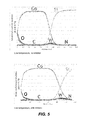
- FIG. 5 shows x-ray photoelectron spectra for cobalt films deposited by ALD with and without inhibitor exposure.
- FIGS. 6 and 7 are schematic illustrations of processing apparatuses suitable for deposition processes in accordance with disclosed embodiments.
- features may be filled with conductive materials.
- conductive materials For example, tungsten is often filled in features to form contacts, such as in front end of line (FEOL) applications.
- FEOL front end of line
- an alternative conductive material such as cobalt, may be used to form contacts or otherwise fill features.
- cobalt deposition in semiconductor fabrication includes electroplating, a wet process that uses an electric current to reduce metal cations in a solution.
- a thin layer of cobalt called a cobalt seed layer, may be first deposited in the feature.
- the seed layer is sufficiently conductive to allow growth of cobalt in the feature in the electroplating process.
- Cobalt may also be deposited by atomic layer deposition (ALD) or chemical vapor deposition (CVD).
- ALD atomic layer deposition
- CVD chemical vapor deposition
- voids may form in the features due to the feature profile.
- FIG. 1A is a schematic illustration of an example of such a feature 100 in a substrate 102 .
- the substrate may be a silicon wafer, e.g., 200-mm wafer, 300-mm wafer, 450-mm wafer, including wafers having one or more layers of material such as dielectric, conducting, or semi-conducting material deposited thereon.
- Features can be characterized by one or more of narrow openings, re-entrant openings, constrictions within the feature, and high aspect ratios.
- the feature 100 may have an aspect ratio of at least about 2:1, at least about 10:1, at least about 15:1, at least about 20:1 or higher.
- the feature 100 may have a dimension near the opening, e.g., an opening diameter or line width, or opening width, or critical dimension, of less than about 19 nm, also known as feature widths less than 1 ⁇ nm.
- the feature 100 can be referred to as an unfilled feature or simply a feature.
- the feature, and any feature may be characterized in part by an axis that extends through the length of the feature, with vertically-oriented features having vertical axes and horizontally-oriented features having horizontal axes.
- the substrate 102 includes a feature 100 having a feature opening 110 which is narrower than the width of the bottom of the feature.
- the feature 100 in FIG. 1A includes a re-entrant profile.
- a re-entrant profile is a profile that narrows from a bottom, closed end, or interior of the feature to the feature opening. According to various embodiments, the profile may narrow gradually and/or include an overhang at the feature opening.
- the re-entrant pattern shown in FIG. 1A may be generated by one or more of asymmetric etching kinetics during patterning and the overhang due to non-conformal film step coverage in the previous film deposition, such as deposition of a diffusion barrier.
- the feature may have a width smaller in the opening at the top of the feature than the width of the bottom of the feature.
- FIG. 1B is a schematic illustration of a barrier layer 104 deposited into the feature 100 . After a barrier layer 104 is deposited, conventional deposition of cobalt by ALD or CVD forms a non-conformal cobalt film in the feature 100 .
- FIG. 1C is a schematic illustration of the feature 100 with a non-conformal film 105 that has overhang at the feature entrance and insufficiently thick film coverage at the bottom of the feature. In a subsequent fill process, a cobalt film 106 is formed.
- a void 160 is region in the feature that is left unfilled.
- a void can form, for example, when the deposited material forms a pinch point within the feature, sealing off an unfilled space within the feature preventing reactant entry and deposition. The formation of voids in features often results in device failure.
- the feature opening is re-entrant, which can contribute to the poor step coverage of the non-conformal film 105 .
- conventional CVD processes for depositing cobalt can result in non-conformality.
- the subsequent fill processes by vapor deposition or by electroplating can result in voids.
- ALD atomic layer deposition
- the methods may be used to deposit any of: cobalt seed layers for subsequent electroplating fill in features, cobalt seed layers for subsequent CVD fill in features, or for direct fill of features by ALD.
- the approaches described herein may be used with narrow features, such as features with sub-10 nm openings, or sub-7 nm openings.
- the methods involve two-step surface treatments during an ALD cycle, with one step involving the reaction of a co-reactant gas with an adsorbed cobalt precursor and the other step involving a growth-inhibiting reactant gas on the cobalt surface.
- the growth-inhibiting reactant gas significantly lowers cobalt growth rate, producing a highly conformal cobalt film.
- the described ALD processes enable improved controllability in film nucleation, step coverage, and morphology by separate surface treatment and low process temperature.
- the methods are applicable to a variety of feature fill applications including the fabrication of metal gate/contact fill in front end of line (FEOL) processes as well as via/line fill in back end of line (BEOL) processes.
- step coverage is defined as a ratio of two thicknesses—the thickness of the material inside the feature divided by the thickness of the material near the opening. If measuring from a middle portion of the feature, the thickness may be measured at a position between about 25% and 75% of the distance or, in certain embodiments, between about 40% and 60% of the distance along the feature's depth measured from the feature's opening. If measuring from an end portion of the feature, the thickness may be measured at a position between about 75% and 95% of the distance along the feature's axis as measured from the opening.
- the terms “near the opening of the feature” and “near the feature's opening” refer to a top portion of the feature located within 25% or, more specifically, within 10% of the opening's edge or other element representative of the opening's edge.
- Step coverage of over 100% can be achieved, for example, by filling a feature wider in the middle or near the bottom of the feature than at the feature opening.
- Conformal depositions have step coverages close to 100%, e.g., 80%-120%, or 90%-110%.
- the methods described herein may be used to deposit cobalt conformally such that the cobalt follows the contours of the underlying surface.
- FIG. 2A is a process flow diagram of operations for performing a method 200 a in accordance with certain embodiments.
- a substrate having a feature to be filled is provided.
- the substrate may be a silicon substrate or another suitable semiconductor substrate.
- the substrate may include more than one feature, and may include a pattern of features having features of various sizes, or features of one size.
- FIG. 2A is discussed in the context of filling a single feature, but it should be understood that features of various sizes may also be filled similarly.
- Features may be any of those described above and may be formed in a dielectric or other material on the substrate.
- a feature formed in silicon oxide or other dielectric may include a metal contact at the feature bottom and dielectric sidewalls.
- the feature includes one or more liner layers that conformally line the feature.
- the one or more liner layers may be one or both of an adhesion layer and diffusion barrier layer.
- barrier layers include thin layer of tungsten nitride (WN), titanium nitride (TiN), tantalum nitride (TaN), and cobalt nitride (CoN).
- adhesion layers include titanium (Ti).
- the barrier film may be a tungsten carbon nitride (WCN) film. WCN barrier films are described, for example, in U.S. patent application Ser. No. 15/474,383, titled “Selective Deposition of WCN Barrier/Adhesion Layer for Interconnect,” filed Mar. 30, 2017, which is incorporated by reference herein.
- the substrate is generally provided to a reaction chamber, examples of which are further described below, in which the ALD deposition of the cobalt layer is performed.
- the below description assumes that the ALD deposition is performed in a single chamber or a single station of a multi-station chamber. However, in alternative embodiments, any of each of the exposure operations may be performed in different chambers or stations.
- the substrate may be provided to a chamber with or without a liner layer previously deposited in a feature.
- Example cobalt precursors include dicarbonyl cyclopentadienyl cobalt (I), cobalt carbonyl, various cobalt amidinate precursors, cobalt diazadienyl complexes, cobalt amidinate/guanidinate precursors, and combinations thereof.
- Suitable cobalt precursors may include a cobalt center with organic groups and/or carbonyl groups, where organic groups include alkyls, such as methyl, ethyl, propyl, butyl, pentyl, hexyl, heptyl, and octyl, which may be straight or branched hydrocarbon chains.
- the cobalt precursor is an organometallic compound that has a substituted or unsubstituted allyl ligand. In some embodiments, the allyl ligand is unsubstituted.
- R 1 is C 1 -C 8 -alkyl
- R 2 is C 1 -C 8 alkyl
- x is zero, 1 or 2
- y is zero or 1.
- R 1 is a C 2 -C 8 -alkyl
- R 2 is independently C 2 -C 8 alkyl.
- alkyl refers to saturated hydrocarbon chain of 1 to 8 atoms in length, such as methyl, ethyl, propyl, butyl, pentyl, hexyl, heptyl, and octyl.
- alkyl includes both straight and branched hydrocarbon chains.
- propyl includes both n-propyl and isopropyl.
- butyl includes both n-butyl, sec-butyl, iso-butyl, and tert-butyl.
- x is 0 and y is 1.
- An example of an organometallic compound in accordance with this embodiment is shown below:
- Certain described compounds are available from SAFC-Hitech of Haverhill, Mass., in conjunction with corresponding deposition apparatuses available from Lam Research Inc., of Fremont, Calif.
- cobalt-containing precursors include metal-organic precursors having a high vapor pressure at low temperatures, such as at temperatures less than about 100° C.
- An example vapor pressure may be about 0.5 Torr in an about 30° C. environment.
- cobalt precursors such as dicobalt hexacarbonyl tert-butylacetylene (CCTBA) are not used.
- CCTBA has a relatively low vapor pressure at low temperatures, which can make it difficult to deposit at low temperatures and is intrinsically unstable, resulting in dimerization or polymerization over time.
- a suitable cobalt precursor is introduced into the chamber using a non-reactive carrier gas, such as argon (Ar).
- a non-reactive carrier gas such as argon (Ar).
- the cobalt precursor is introduced to the chamber using argon as a carrier gas.
- the cobalt precursor is adsorbed onto the substrate such that it conformally lines the feature surface. Un-adsorbed cobalt precursor is then purged from the chamber in an operation 206 . Purging can involve one or both of introducing an inert gas to sweep the chamber and a vacuum purge.
- the feature is then exposed to a co-reactant dose in an operation 208 .
- the co-reactant is a compound that reacts with the adsorbed cobalt precursor to form cobalt.
- the co-reactant is hydrogen (H 2 ), though other co-reactants may be used depending on the cobalt precursor chemistry.
- the co-reactant may be introduced using a non-reactant carrier gas. The adsorbed precursor is reacted and forms cobalt metal on the feature surface.
- the feature is then exposed to an inhibitor-containing reactant dose in an operation 210 .
- the inhibitor-containing reactant dose is a nitrogen-containing dose, with examples including ammonia (NH 3 ), nitrogen (N 2 ), and hydrazine (N 2 H 2 ).
- Other nitrogen-containing compounds may be used as cobalt growth inhibitors.
- Operation 210 may further involve introducing the co-reactant gas that was introduced in operation 208 along with the inhibitor-containing reactant gas.
- the inhibitor-containing reactant gas interacts with the cobalt (Co) and serves to inhibit cobalt growth.
- too much NH 3 or other inhibitor can result in unacceptably slow or stopped growth or the incorporation of nitrogen into the cobalt film.
- transitioning from operation 208 to operation 210 involves continuing to flow the co-reactant into the chamber and adding a flow of the inhibitor-containing reactant gas.
- the chamber is then purged in an operation 212 .
- the cycle is to be repeated, the method returns to operation 204 . If not, the method ends. The cycle is generally repeated until a desired thickness of cobalt is deposited.
- that thickness can be enough for a cobalt seed layer to support subsequent bulk vapor deposition or electroplating or can be sufficient to fill a feature.
- the feature may be only partially filled, with a subsequent CVD bulk deposition of cobalt or an electroplating operation performed to complete feature fill.
- the feature may be filled.
- FIG. 2B is a process flow diagram of operations for performing a method 200 b in accordance with certain embodiments.
- the method 200 b differs from the method 200 a discussed with reference to FIG. 2A in that exposing the substrate to the inhibitor-containing reactor dose (operation 210 ) is performed prior to exposing the substrate to the co-reactant dose with inhibitor (operation 208 ). Transitioning from operation 210 to operation 208 in the method 200 b may involve shutting off a flow of the inhibitor-containing reactant gas while continuing to flow the co-reactant.
- the inhibitor-containing reactant dose may be 0.5% to 20% (volumetric) of the combined inhibitor-containing reactant dose and co-reactant dose. In particular embodiments, it may be 1% to 5% (volumetric).
- Operations 202 , 204 , 206 , and 212 may be performed as described above with respect to FIG. 2 a .
- the methods 200 a and 200 b in FIGS. 2A and 2B are thermal, non-plasma ALD processes.
- Substrate temperature during the ALD deposition is relatively low, for example, below 150° C., and in some embodiments, below 100° C. Temperature is generally no lower than 70° C.
- the chamber pressure may be between 5 Torr to 50 Torr and in some embodiments between 8 Torr and 20 Torr. Substrate temperature affects the step coverage such that by operating at relatively low temperatures, better step coverage can be obtained. Pressure affects film qualities such as impurity levels and resistivity. In some embodiments, pressure is at least 8 Torr to obtain highly pure cobalt films with low resistivity.
- the suitable cobalt-containing precursor and/or reducing agent are introduced into the chamber using a carrier gas, such as argon (Ar).
- a carrier gas such as argon (Ar).
- Example flow rates are given below, with the understanding that the flow rates will depend on the particular deposition chamber used and may vary from the examples given.
- the flow rate of an Ar carrier gas or other carrier gas that carries the cobalt precursor may be between about 15 sccm and about 300 sccm, and in more particular embodiments between about 50 sccm and about 100 sccm.
- the Ar or other purge gas flow rate may be between 10 sccm and 50,000 sccm, and in more particular embodiments, between 500 sccm and 10,000 sccm.
- no reactants or inhibitor gases may be flowed.
- the co-reactant is hydrogen (H 2 ).
- H 2 may be flowed without a carrier gas in some embodiments.
- the H 2 co-reactant may be introduced at a flow rate between about 100 sccm and about 50,000 sccm, or more particularly, between about 500 sccm and about 10,000 sccm.
- the inhibitor gas is NH 3 .
- the NH 3 may be introduced at a flow rate of between 5 sccm and 2,000 sccm, or more particularly, 10 sccm to 400 sccm.
- the inhibitor compound is one that inhibits nucleation or adsorption of the cobalt precursor without being incorporated into the film.
- nitrogen-containing inhibitor compounds have been found to have an inhibiting effect. Oxygen, halogen, and other reactive species may be avoided.
- the inhibitor compound may be referred to as a cobalt growth inhibitor or an inhibitor.
- FIG. 3 is a graph showing the effect of inhibitor exposure on the ALD growth rate of cobalt.
- Three ALD processes are compared: a high temperature process with no inhibitor exposure (data points marked with circles), a low temperature process with no inhibitor exposure (squares), and a low temperature process with inhibitor exposure (triangles).
- the high temperature process refers to a temperature in the range 100° C. to 140° C., with the low temperature processes referring to a temperature about 20-40° C. less than the high temperature process.
- the low temperature process with inhibitor exposure was performed according to the method 200 a shown in FIG. 2A .
- a cobalt precursor according to structure II was used, with H 2 as the co-reactant and an H 2 /NH 3 mixture used for inhibitor exposure.
- NH 3 was 1-2% volumetric of the H 2 /NH 3 mixture.
- FIG. 3 shows that growth rate is affected by temperature, with the growth rate dropping by 45% with a decreased in temperature.
- the inhibitor dose is even more effective at slowing growth rate, with a drop of 65%. In this manner, the ALD process is slower, which results in greater conformality and step coverage.
- FIG. 4A shows transmission electron microscope (TEM) images of ALD cobalt films on trenches with a top critical dimension (CD) opening of 22-27 nm.
- the left image shows ALD cobalt deposition using a high temperature process as described with reference to FIG. 3 and no inhibitor exposure.
- the right image shows ALD cobalt deposition using a low temperature process with inhibitor exposure as described with reference to FIG. 3 .
- the film step coverage and film morphology is improved by using a lower temperature and inhibitor exposure.
- FIG. 4B shows a TEM image of cobalt gapfill using an ALD process as described above with respect to FIG. 2A .
- FIG. 5 shows x-ray photoelectron spectra for cobalt films deposited by ALD with and without inhibitor exposure. The spectra show that there is negligible nitrogen impurities and similar carbon content for the two films. This indicates that there is no inhibitor-associated impurity incorporated into the film.
- FIG. 6 depicts a schematic illustration of an embodiment of an ALD process station 600 having a process chamber 602 for maintaining a low-pressure environment.
- a plurality of ALD process stations may be included in a common low pressure process tool environment.
- FIG. 7 depicts an embodiment of a multi-station processing tool 700 .
- one or more hardware parameters of ALD process station 600 may be adjusted programmatically by one or more computer controllers 650 .
- ALD process station 600 fluidly communicates with reactant delivery system 601 a for delivering process gases to a distribution showerhead 606 .
- Reactant delivery system 601 a includes a mixing vessel 604 for blending and/or conditioning process gases, such as a cobalt precursor gas, hydrogen-containing gas, or nitrogen-containing gas, for delivery to showerhead 606 .
- One or more mixing vessel inlet valves 620 may control introduction of process gases to mixing vessel 604 .
- deposition of a cobalt film is performed in process station 600 and in some embodiments, other operations such as barrier layer deposition or cobalt gap fill may be performed in the same or another station of the multi-station processing tool 700 as further described below with respect to FIG. 7 .
- the embodiment of FIG. 6 includes a vaporization point 603 for vaporizing liquid reactant to be supplied to the mixing vessel 604 .
- vaporization point 603 may be a heated vaporizer.
- a liquid precursor or liquid reactant may be vaporized at a liquid injector (not shown).
- a liquid injector may inject pulses of a liquid reactant into a carrier gas stream upstream of the mixing vessel 604 .
- a liquid injector may vaporize the reactant by flashing the liquid from a higher pressure to a lower pressure.
- a liquid injector may atomize the liquid into dispersed microdroplets that are subsequently vaporized in a heated delivery pipe.
- a liquid injector may be mounted directly to mixing vessel 604 .
- a liquid injector may be mounted directly to showerhead 606 .
- a liquid flow controller (LFC) upstream of vaporization point 603 may be provided for controlling a mass flow of liquid for vaporization and delivery to process chamber 602 .
- the LFC may include a thermal mass flow meter (MFM) located downstream of the LFC.
- a plunger valve of the LFC may then be adjusted responsive to feedback control signals provided by a proportional-integral-derivative (PID) controller in electrical communication with the MFM.
- PID proportional-integral-derivative
- the LFC may be dynamically switched between a feedback control mode and a direct control mode. In some embodiments, this may be performed by disabling a sense tube of the LFC and the PID controller.
- showerhead 606 distributes process gases toward substrate 612 .
- the substrate 612 is located beneath showerhead 606 and is shown resting on a pedestal 608 .
- showerhead 606 may have any suitable shape, and may have any suitable number and arrangement of ports for distributing process gases to substrate 612 .
- pedestal 608 may be raised or lowered to expose substrate 612 to a volume between the substrate 612 and the showerhead 606 .
- pedestal 808 may be temperature controlled via heater 610 .
- Pedestal 608 may be set to any suitable temperature, such as between about 25° C. and about 650° C. during operations for performing various disclosed embodiments. As described above, the pedestal temperature may be between 50° C. and 150° C., or 50° C. and 100° C. during ALD deposition of the cobalt film. It will be appreciated that, in some embodiments, pedestal height may be adjusted programmatically by a suitable computer controller 650 . At the conclusion of a process phase, pedestal 608 may be lowered during another substrate transfer phase to allow removal of substrate 612 from pedestal 608 .
- a position of showerhead 606 may be adjusted relative to pedestal 608 to vary a volume between the substrate 612 and the showerhead 606 .
- a vertical position of pedestal 608 and/or showerhead 606 may be varied by any suitable mechanism within the scope of the present disclosure.
- pedestal 608 may include a rotational axis for rotating an orientation of substrate 612 .
- one or more of these example adjustments may be performed programmatically by one or more suitable computer controllers 650 .
- the computer controller 650 may include any of the features described below with respect to controller 750 of FIG. 9 .
- instructions for a controller 650 may be provided via input/output control (IOC) sequencing instructions.
- the instructions for setting conditions for a process phase may be included in a corresponding recipe phase of a process recipe.
- process recipe phases may be sequentially arranged, so that all instructions for a process phase are executed concurrently with that process phase.
- instructions for setting one or more reactor parameters may be included in a recipe phase.
- a first recipe phase may include instructions for setting a flow rate of an inert and/or a reactant gas (e.g., the first precursor such as a cobalt precursor), instructions for setting a flow rate of a carrier gas (such as argon), and time delay instructions for the first recipe phase.
- a second, subsequent recipe phase may include instructions for modulating or stopping a flow rate of an inert and/or a reactant gas, and instructions for modulating a flow rate of a carrier or purge gas and time delay instructions for the second recipe phase.
- a third recipe phase may include instructions for modulating a flow rate of a second reactant gas such as H 2 or NH 3 , instructions for modulating the flow rate of a carrier or purge gas, instructions for igniting a plasma, and time delay instructions for the third recipe phase.
- a fourth, subsequent recipe phase may include instructions for modulating or stopping a flow rate of an inert and/or a reactant gas, and instructions for modulating a flow rate of a carrier or purge gas and time delay instructions for the fourth recipe phase. It will be appreciated that these recipe phases may be further subdivided and/or iterated in any suitable way within the scope of the present disclosure.
- pressure control for process station 600 may be provided by butterfly valve 618 . As shown in the embodiment of FIG. 6 , butterfly valve 618 throttles a vacuum provided by a downstream vacuum pump (not shown). However, in some embodiments, pressure control of process station 600 may also be adjusted by varying a flow rate of one or more gases introduced to the process station 600 .
- FIG. 7 shows a schematic view of an embodiment of a multi-station processing tool 700 with an inbound load lock 702 and an outbound load lock 704 , either or both of which may include a remote plasma source (not shown).
- a robot 706 at atmospheric pressure, is configured to move wafers from a cassette loaded through a pod 708 into inbound load lock 702 via an atmospheric port 710 .
- a wafer (not shown) is placed by the robot 706 on a pedestal 712 in the inbound load lock 702 , the atmospheric port 710 is closed, and the load lock inbound 702 is pumped down.
- the wafer may be exposed to a remote plasma treatment in the inbound load lock 702 prior to being introduced into a processing chamber 714 . Further, the wafer also may be heated in the inbound load lock 702 as well, for example, to remove moisture and adsorbed gases. Next, a chamber transport port 716 to processing chamber 714 is opened, and another robot (not shown) places the wafer into the reactor on a pedestal of a first station shown in the reactor for processing. While the embodiment depicted in FIG. 7 includes load locks, it will be appreciated that, in some embodiments, direct entry of a wafer into a process station may be provided.
- the depicted processing chamber 714 includes four process stations, numbered from 1 to 4 in the embodiment shown in FIG. 7 .
- Each station has a heated pedestal (shown at 718 for station 1 ), and gas line inlets.
- each process station may have different or multiple purposes.
- a process station may be switchable between an ALD and plasma-enhanced ALD process mode.
- exposure to a deposition precursor and exposure to a second reactant and plasma are performed in the same station.
- processing chamber 714 may include one or more matched pairs of ALD and plasma-enhanced ALD process stations.
- processing chamber 714 includes four stations, it will be understood that a processing chamber according to the present disclosure may have any suitable number of stations. For example, in some embodiments, a processing chamber may have five or more stations, while in other embodiments a processing chamber may have three or fewer stations.
- FIG. 9 depicts an embodiment of a wafer handling system 790 for transferring wafers within processing chamber 714 .
- wafer handling system 790 may transfer wafers between various process stations and/or between a process station and a load lock. It will be appreciated that any suitable wafer handling system may be employed. Non-limiting examples include wafer carousels and wafer handling robots.
- FIG. 7 also depicts an embodiment of a system controller 750 employed to control process conditions and hardware states of process tool 700 .
- System controller 750 may include one or more memory devices 756 , one or more mass storage devices 754 , and one or more processors 752 .
- Processor 752 may include a CPU or computer, analog, and/or digital input/output connections, stepper motor controller boards, etc.
- system controller 750 controls all of the activities of process tool 700 .
- System controller 750 executes system control software 758 stored in mass storage device 754 , loaded into memory device 756 , and executed on processor 752 .
- the control logic may be hard coded in the controller 750 .
- Applications Specific Integrated Circuits, Programmable Logic Devices e.g., field-programmable gate arrays, or FPGAs
- FPGAs field-programmable gate arrays
- System control software 758 may include instructions for controlling the timing, mixture of gases, gas flow rates, chamber and/or station pressure, chamber and/or station temperature, plasma exposure duration, UV radiation duration, wafer temperature, target power levels, RF power levels, substrate pedestal, chuck and/or susceptor position, and other parameters of a particular process performed by process tool 700 .
- System control software 758 may be configured in any suitable way. For example, various process tool component subroutines or control objects may be written to control operation of the process tool components used to carry out various process tool processes.
- System control software 758 may be coded in any suitable computer readable programming language.
- system control software 758 may include input/output control (IOC) sequencing instructions for controlling the various parameters described above.
- IOC input/output control
- Other computer software and/or programs stored on mass storage device 754 and/or memory device 756 associated with system controller 750 may be employed in some embodiments. Examples of programs or sections of programs for this purpose include a substrate positioning program, a process gas control program, a pressure control program, a heater control program, and a plasma control program.
- a substrate positioning program may include program code for process tool components that are used to load the substrate onto pedestal 718 and to control the spacing between the substrate and other parts of process tool 700 .
- a process gas control program may include code for controlling gas composition (e.g., cobalt precursor gases, co-reactant gases, inhibitor gases, and purge gases as described herein) and flow rates and optionally for flowing gas into one or more process stations prior to deposition in order to stabilize the pressure in the process station.
- a pressure control program may include code for controlling the pressure in the process station by regulating, for example, a throttle valve in the exhaust system of the process station, a gas flow into the process station, etc.
- a heater control program may include code for controlling the current to a heating unit that is used to heat the substrate.
- the heater control program may control delivery of a heat transfer gas (such as helium) to the substrate.
- a pressure control program may include code for maintaining the pressure in the reaction chamber in accordance with the embodiments herein.
- the user interface may include a display screen, graphical software displays of the apparatus and/or process conditions, and user input devices such as pointing devices, keyboards, touch screens, microphones, etc.
- parameters adjusted by system controller 750 may relate to process conditions.
- Non-limiting examples include process gas composition and flow rates, temperature, pressure, etc. These parameters may be provided to the user in the form of a recipe, which may be entered utilizing the user interface.
- Signals for monitoring the process may be provided by analog and/or digital input connections of system controller 750 from various process tool sensors.
- the signals for controlling the process may be output on the analog and digital output connections of process tool 700 .
- process tool sensors that may be monitored include mass flow controllers, pressure sensors (such as manometers), thermocouples, etc. Appropriately programmed feedback and control algorithms may be used with data from these sensors to maintain process conditions.
- System controller 750 may provide program instructions for implementing the above-described deposition processes.
- the program instructions may control a variety of process parameters, such as pressure, temperature, etc.
- the instructions may control the parameters to operate in-situ deposition of film stacks according to various embodiments described herein.
- the system controller 750 will typically include one or more memory devices and one or more processors configured to execute the instructions so that the apparatus will perform a method in accordance with disclosed embodiments.
- Machine-readable media containing instructions for controlling process operations in accordance with disclosed embodiments may be coupled to the system controller 750 .
- the system controller 750 is part of a system, which may be part of the above-described examples.
- Such systems can include semiconductor processing equipment, including a processing tool or tools, chamber or chambers, a platform or platforms for processing, and/or specific processing components (a wafer pedestal, a gas flow system, etc.).
- These systems may be integrated with electronics for controlling their operation before, during, and after processing of a semiconductor wafer or substrate.
- the electronics may be referred to as the “controller,” which may control various components or subparts of the system or systems.
- the system controller 750 may be programmed to control any of the processes disclosed herein, including the delivery of processing gases, temperature settings (e.g., heating and/or cooling), pressure settings, vacuum settings, flow rate settings, fluid delivery settings, positional and operation settings, wafer transfers into and out of a tool and other transfer tools and/or load locks connected to or interfaced with a specific system.
- the system controller 750 may be defined as electronics having various integrated circuits, logic, memory, and/or software that receive instructions, issue instructions, control operation, enable cleaning operations, enable endpoint measurements, and the like.
- the integrated circuits may include chips in the form of firmware that store program instructions, digital signal processors (DSPs), chips defined as application specific integrated circuits (ASICs), and/or one or more microprocessors, or microcontrollers that execute program instructions (e.g., software).
- Program instructions may be instructions communicated to the system controller 750 in the form of various individual settings (or program files), defining operational parameters for carrying out a particular process on or for a semiconductor wafer or to a system.
- the operational parameters may, in some embodiments, be part of a recipe defined by process engineers to accomplish one or more processing steps during the fabrication of one or more layers, materials, metals, oxides, silicon, silicon dioxide, surfaces, circuits, and/or dies of a wafer.
- the system controller 750 may be a part of or coupled to a computer that is integrated with, coupled to the system, otherwise networked to the system, or a combination thereof.
- the system controller 750 may be in the “cloud” or all or a part of a fab host computer system, which can allow for remote access of the wafer processing.
- the computer may enable remote access to the system to monitor current progress of fabrication operations, examine a history of past fabrication operations, examine trends or performance metrics from a plurality of fabrication operations, to change parameters of current processing, to set processing steps to follow a current processing, or to start a new process.
- a remote computer e.g.
- a server can provide process recipes to a system over a network, which may include a local network or the Internet.
- the remote computer may include a user interface that enables entry or programming of parameters and/or settings, which are then communicated to the system from the remote computer.
- the system controller 750 receives instructions in the form of data, which specify parameters for each of the processing steps to be performed during one or more operations. It should be understood that the parameters may be specific to the type of process to be performed and the type of tool that the system controller 750 is configured to interface with or control. Thus as described above, the system controller 750 may be distributed, such as by including one or more discrete controllers that are networked together and working towards a common purpose, such as the processes and controls described herein.
- FIGS. 6 and 7 provide examples of chambers and tools that may be used to perform the methods disclosed herein, various modifications may be made.
- example systems may include a plasma etch chamber or module, a deposition chamber or module, a spin-rinse chamber or module, a metal plating chamber or module, a clean chamber or module, a bevel edge etch chamber or module, a physical vapor deposition (PVD) chamber or module, a chemical vapor deposition (CVD) chamber or module, an ALD chamber or module, an atomic layer etch (ALE) chamber or module, an ion implantation chamber or module, a track chamber or module, and any other semiconductor processing systems that may be associated or used in the fabrication and/or manufacturing of semiconductor wafers.
- PVD physical vapor deposition
- CVD chemical vapor deposition
- ALD atomic layer etch
- ALE atomic layer etch
- the system controller 750 might communicate with one or more of other tool circuits or modules, other tool components, cluster tools, other tool interfaces, adjacent tools, neighboring tools, tools located throughout a factory, a main computer, another controller, or tools used in material transport that bring containers of wafers to and from tool locations and/or load ports in a semiconductor manufacturing factory.
Landscapes
- Chemical & Material Sciences (AREA)
- Engineering & Computer Science (AREA)
- Chemical Kinetics & Catalysis (AREA)
- General Chemical & Material Sciences (AREA)
- Materials Engineering (AREA)
- Mechanical Engineering (AREA)
- Metallurgy (AREA)
- Organic Chemistry (AREA)
- General Physics & Mathematics (AREA)
- Physics & Mathematics (AREA)
- Condensed Matter Physics & Semiconductors (AREA)
- Manufacturing & Machinery (AREA)
- Computer Hardware Design (AREA)
- Microelectronics & Electronic Packaging (AREA)
- Power Engineering (AREA)
- Electrodes Of Semiconductors (AREA)
- Chemical Vapour Deposition (AREA)
Abstract
Provided herein are atomic layer deposition (ALD) methods of depositing cobalt in a feature. The methods involve two-step surface treatments during an ALD cycle, with one step involving the reaction of a co-reactant gas with an adsorbed cobalt precursor and the other step involving a growth-inhibiting reactant gas on the cobalt surface. The growth-inhibiting reactant gas significantly lowers cobalt growth rate, producing a highly conformal cobalt film. The described ALD processes enable improved controllability in film nucleation, step coverage, and morphology by the separate surface treatment and low process temperature. The methods are applicable to a variety of feature fill applications including the fabrication of metal gate/contact fill in front end of line (FEOL) processes as well as via/line fill in back end of line (BEOL) processes.
Description
Semiconductor device fabrication often involves deposition of tungsten-containing materials to be used for horizontal interconnects, vias between adjacent metal layers, and contacts between first metal layers and devices on the silicon substrate. In a conventional deposition process, tungsten is deposited in a chemical vapor deposition (CVD) process by exposing the substrate to a tungsten-containing precursor and a reducing agent.
However, as devices shrink, features become narrower and aspect ratios increase dramatically resulting in various challenges in depositing tungsten. As a result, alternative materials are sought to fill features. Cobalt is considered a promising candidate because of its low electron mean free path and good electro-migration performance. However, current processes for depositing cobalt have various challenges including non-conformal deposition in features, which can cause one or both of overhang on a feature entrance and insufficient coverage on the bottom of the feature. Non-conformal deposition can lead to voids in the feature.
Provided herein are methods of atomic layer deposition (ALD) of cobalt films and related apparatus. One aspect of the subject matter disclosed herein relates to a method of depositing cobalt in a feature. The method involves providing a substrate having one or more features, each feature having a feature opening and performing multiple cycles of to deposit a cobalt layer that is conformal to the one or more features. Each cycle includes exposing the feature to a dose of a cobalt precursor to form a layer of adsorbed cobalt precursor on the one or more features, exposing the layer of adsorbed cobalt precursor to a dose of a co-reactant to react with the layer of adsorbed cobalt precursor on the one or more features, and exposing the feature to a dose of a mixture of the co-reactant and a nitrogen-containing cobalt growth inhibitor.
In some embodiments, exposing the adsorbed cobalt precursor to the dose of the co-reactant to react with the layer of adsorbed cobalt precursor on the one or more features is performed prior to exposing the feature to the dose of the mixture of the co-reactant and the nitrogen-containing cobalt growth inhibitor.
In some embodiments, exposing the adsorbed cobalt precursor to the dose of the co-reactant to react with the layer of adsorbed cobalt precursor on the one or more features is performed after exposing the feature to the dose of the mixture of the co-reactant and the nitrogen-containing cobalt growth inhibitor.
In some embodiments, the cobalt precursor has a structure according to (I):

where R1 is C1-C8-alkyl, R2 is C1-C8 alkyl, x is zero, 1 or 2; and y is zero or 1.
In some embodiments, the cobalt precursor has a structure according to (II).

In some embodiments, the cobalt precursor is selected from the group consisting of dicarbonyl cyclopentadienyl cobalt, cobalt carbonyl, a cobalt amidinate precursor, a cobalt diazadienyl complex, and a cobalt amidinate/guanidinate precursor.
According to various embodiments, the substrate temperature during the multiple cycles is maintained at a temperature no more than 150° C., no more than 100° C., or no more than 90° C.
In some embodiments, the cobalt layer is deposited on a barrier layer.
In some embodiments, the co-reactant is hydrogen (H2). In some embodiments, the co-reactant is hydrogen (H2) and the nitrogen-containing cobalt inhibitor is ammonia (NH3). In some embodiments, the NH3 is between 0.5% and 20% (volumetric) of the mixture, or between 0.5% and 5% (volumetric) of the mixture.
In some embodiments, each cycle further involves purging a chamber in which the substrate is housed after exposing the feature to the dose of the cobalt precursor and prior to exposing the adsorbed cobalt precursor to the dose of the co-reactant.
In some embodiments, each cycle further involves purging a chamber in which the substrate is housed after exposing the feature to the dose of a mixture of the co-reactant and the nitrogen-containing cobalt growth inhibitor.
In some embodiments, there is no purge between exposing the feature to the dose of the co-reactant and exposing the feature to the dose of the mixture of the co-reactant and the nitrogen-containing cobalt growth inhibitor.
Another aspect of the disclosure relates to a method including: (a) introducing a dose of a cobalt precursor to a process chamber, (b) after introducing the dose of the cobalt precursor, purging the process chamber, (c) after purging the process chamber, introducing a dose of a H2 co-reactant, (d) after introducing the dose of the H2 co-reactant, introducing a dose of a mixture of the H2 co-reactant and a nitrogen-containing compound, wherein the nitrogen-containing compound is between 0.5% and 20% (volumetric) of the total of the H2 co-reactant and the nitrogen-containing compound; (e) after introducing the dose of the mixture of the H2 co-reactant and a nitrogen-containing compound, purging the process chamber; and repeating (a)-(e) one or more times.
Another aspect of the disclosure relates to an apparatus comprising: a process chamber; one or more gas inlets into the process chamber and associated flow-control hardware; and a controller having at least one processor and a memory, wherein the at least one processor and the memory are communicatively connected with one another, the at least one processor is at least operatively connected with the flow-control hardware, and the memory stores computer-executable instructions for: (a) introducing a dose of a cobalt precursor to the process chamber; (b) after introducing the dose of the cobalt precursor, purging the process chamber; (c) after purging the process chamber, introducing a dose of a H2 co-reactant; (d) after introducing the dose of the H2 co-reactant, introducing a dose of a mixture of the H2 co-reactant and a nitrogen-containing compound, wherein the nitrogen-containing compound is between 0.5% and 20% (volumetric) of the total of the H2 co-reactant and the nitrogen-containing compound; (e) after introducing the dose of the mixture of the H2 co-reactant and a nitrogen-containing compound, purging the chamber; and repeating (a)-(e) one or more times.
These and other aspects are described further below with reference to the drawings.
In the following description, numerous specific details are set forth to provide a thorough understanding of the presented embodiments. The disclosed embodiments may be practiced without some or all of these specific details. In other instances, well-known process operations have not been described in detail to not unnecessarily obscure the disclosed embodiments. While the disclosed embodiments will be described in conjunction with the specific embodiments, it will be understood that it is not intended to limit the disclosed embodiments.
In semiconductor fabrication, features may be filled with conductive materials. For example, tungsten is often filled in features to form contacts, such as in front end of line (FEOL) applications. However, as devices shrink, aspect ratios increase and smaller features are used to form contacts. In many applications, an alternative conductive material, such as cobalt, may be used to form contacts or otherwise fill features.
Conventional cobalt deposition in semiconductor fabrication includes electroplating, a wet process that uses an electric current to reduce metal cations in a solution. In cobalt electroplating, a thin layer of cobalt, called a cobalt seed layer, may be first deposited in the feature. The seed layer is sufficiently conductive to allow growth of cobalt in the feature in the electroplating process.
Cobalt may also be deposited by atomic layer deposition (ALD) or chemical vapor deposition (CVD). In conventional ALD or CVD, voids may form in the features due to the feature profile. FIG. 1A is a schematic illustration of an example of such a feature 100 in a substrate 102. The substrate may be a silicon wafer, e.g., 200-mm wafer, 300-mm wafer, 450-mm wafer, including wafers having one or more layers of material such as dielectric, conducting, or semi-conducting material deposited thereon. Features can be characterized by one or more of narrow openings, re-entrant openings, constrictions within the feature, and high aspect ratios. In some embodiments, the feature 100 may have an aspect ratio of at least about 2:1, at least about 10:1, at least about 15:1, at least about 20:1 or higher. The feature 100 may have a dimension near the opening, e.g., an opening diameter or line width, or opening width, or critical dimension, of less than about 19 nm, also known as feature widths less than 1× nm. The feature 100 can be referred to as an unfilled feature or simply a feature. The feature, and any feature, may be characterized in part by an axis that extends through the length of the feature, with vertically-oriented features having vertical axes and horizontally-oriented features having horizontal axes.
As shown, the substrate 102 includes a feature 100 having a feature opening 110 which is narrower than the width of the bottom of the feature. The feature 100 in FIG. 1A includes a re-entrant profile. A re-entrant profile is a profile that narrows from a bottom, closed end, or interior of the feature to the feature opening. According to various embodiments, the profile may narrow gradually and/or include an overhang at the feature opening. The re-entrant pattern shown in FIG. 1A may be generated by one or more of asymmetric etching kinetics during patterning and the overhang due to non-conformal film step coverage in the previous film deposition, such as deposition of a diffusion barrier. In various examples, the feature may have a width smaller in the opening at the top of the feature than the width of the bottom of the feature. FIG. 1B is a schematic illustration of a barrier layer 104 deposited into the feature 100. After a barrier layer 104 is deposited, conventional deposition of cobalt by ALD or CVD forms a non-conformal cobalt film in the feature 100. FIG. 1C is a schematic illustration of the feature 100 with a non-conformal film 105 that has overhang at the feature entrance and insufficiently thick film coverage at the bottom of the feature. In a subsequent fill process, a cobalt film 106 is formed. Due to the overhang at the feature entrance and insufficient coverage at the feature bottom, the fill process results in the formation of a void 160 within the pattern of the feature 100. A void is region in the feature that is left unfilled. A void can form, for example, when the deposited material forms a pinch point within the feature, sealing off an unfilled space within the feature preventing reactant entry and deposition. The formation of voids in features often results in device failure.
In the example of FIGS. 1A-1D , the feature opening is re-entrant, which can contribute to the poor step coverage of the non-conformal film 105. However, even in features that are not re-entrant, conventional CVD processes for depositing cobalt can result in non-conformality. The subsequent fill processes by vapor deposition or by electroplating can result in voids.
Provided herein are atomic layer deposition (ALD) methods of depositing cobalt. The methods may be used to deposit any of: cobalt seed layers for subsequent electroplating fill in features, cobalt seed layers for subsequent CVD fill in features, or for direct fill of features by ALD. The approaches described herein may be used with narrow features, such as features with sub-10 nm openings, or sub-7 nm openings. The methods involve two-step surface treatments during an ALD cycle, with one step involving the reaction of a co-reactant gas with an adsorbed cobalt precursor and the other step involving a growth-inhibiting reactant gas on the cobalt surface. The growth-inhibiting reactant gas significantly lowers cobalt growth rate, producing a highly conformal cobalt film. The described ALD processes enable improved controllability in film nucleation, step coverage, and morphology by separate surface treatment and low process temperature. The methods are applicable to a variety of feature fill applications including the fabrication of metal gate/contact fill in front end of line (FEOL) processes as well as via/line fill in back end of line (BEOL) processes.
The distribution of a material within a feature may be characterized by its step coverage. For the purposes of this description, “step coverage” is defined as a ratio of two thicknesses—the thickness of the material inside the feature divided by the thickness of the material near the opening. If measuring from a middle portion of the feature, the thickness may be measured at a position between about 25% and 75% of the distance or, in certain embodiments, between about 40% and 60% of the distance along the feature's depth measured from the feature's opening. If measuring from an end portion of the feature, the thickness may be measured at a position between about 75% and 95% of the distance along the feature's axis as measured from the opening. The terms “near the opening of the feature” and “near the feature's opening” refer to a top portion of the feature located within 25% or, more specifically, within 10% of the opening's edge or other element representative of the opening's edge. Step coverage of over 100% can be achieved, for example, by filling a feature wider in the middle or near the bottom of the feature than at the feature opening. Conformal depositions have step coverages close to 100%, e.g., 80%-120%, or 90%-110%. The methods described herein may be used to deposit cobalt conformally such that the cobalt follows the contours of the underlying surface.
In some embodiments, the feature includes one or more liner layers that conformally line the feature. The one or more liner layers may be one or both of an adhesion layer and diffusion barrier layer. Examples of barrier layers include thin layer of tungsten nitride (WN), titanium nitride (TiN), tantalum nitride (TaN), and cobalt nitride (CoN). Examples of adhesion layers include titanium (Ti). In some embodiments, the barrier film may be a tungsten carbon nitride (WCN) film. WCN barrier films are described, for example, in U.S. patent application Ser. No. 15/474,383, titled “Selective Deposition of WCN Barrier/Adhesion Layer for Interconnect,” filed Mar. 30, 2017, which is incorporated by reference herein.
The substrate is generally provided to a reaction chamber, examples of which are further described below, in which the ALD deposition of the cobalt layer is performed. The below description assumes that the ALD deposition is performed in a single chamber or a single station of a multi-station chamber. However, in alternative embodiments, any of each of the exposure operations may be performed in different chambers or stations. The substrate may be provided to a chamber with or without a liner layer previously deposited in a feature.
The feature is then exposed to a cobalt precursor dose in an operation 204. Example cobalt precursors include dicarbonyl cyclopentadienyl cobalt (I), cobalt carbonyl, various cobalt amidinate precursors, cobalt diazadienyl complexes, cobalt amidinate/guanidinate precursors, and combinations thereof. Suitable cobalt precursors may include a cobalt center with organic groups and/or carbonyl groups, where organic groups include alkyls, such as methyl, ethyl, propyl, butyl, pentyl, hexyl, heptyl, and octyl, which may be straight or branched hydrocarbon chains. In some embodiments, the cobalt precursor is an organometallic compound that has a substituted or unsubstituted allyl ligand. In some embodiments, the allyl ligand is unsubstituted.
In some embodiments the cobalt precursor is an organometallic cobalt compound having the following structure:

where R1 is C1-C8-alkyl, R2 is C1-C8 alkyl, x is zero, 1 or 2; and y is zero or 1.
In some embodiments R1 is a C2-C8-alkyl, R2 is independently C2-C8 alkyl.
The term “alkyl” as used herein refers to saturated hydrocarbon chain of 1 to 8 atoms in length, such as methyl, ethyl, propyl, butyl, pentyl, hexyl, heptyl, and octyl. The term “alkyl” includes both straight and branched hydrocarbon chains. Thus, the term propyl includes both n-propyl and isopropyl. The term butyl includes both n-butyl, sec-butyl, iso-butyl, and tert-butyl.
In some embodiments x is 0 and y is 1. An example of an organometallic compound in accordance with this embodiment is shown below:

Certain described compounds are available from SAFC-Hitech of Haverhill, Mass., in conjunction with corresponding deposition apparatuses available from Lam Research Inc., of Fremont, Calif.
In some embodiments, cobalt-containing precursors include metal-organic precursors having a high vapor pressure at low temperatures, such as at temperatures less than about 100° C. An example vapor pressure may be about 0.5 Torr in an about 30° C. environment. In some embodiments, cobalt precursors such as dicobalt hexacarbonyl tert-butylacetylene (CCTBA) are not used. CCTBA has a relatively low vapor pressure at low temperatures, which can make it difficult to deposit at low temperatures and is intrinsically unstable, resulting in dimerization or polymerization over time.
In various embodiments, a suitable cobalt precursor is introduced into the chamber using a non-reactive carrier gas, such as argon (Ar). In some embodiments, the cobalt precursor is introduced to the chamber using argon as a carrier gas. The cobalt precursor is adsorbed onto the substrate such that it conformally lines the feature surface. Un-adsorbed cobalt precursor is then purged from the chamber in an operation 206. Purging can involve one or both of introducing an inert gas to sweep the chamber and a vacuum purge. The feature is then exposed to a co-reactant dose in an operation 208. The co-reactant is a compound that reacts with the adsorbed cobalt precursor to form cobalt. In the examples provided herein, the co-reactant is hydrogen (H2), though other co-reactants may be used depending on the cobalt precursor chemistry. In some embodiments, the co-reactant may be introduced using a non-reactant carrier gas. The adsorbed precursor is reacted and forms cobalt metal on the feature surface.
The feature is then exposed to an inhibitor-containing reactant dose in an operation 210. The inhibitor-containing reactant dose is a nitrogen-containing dose, with examples including ammonia (NH3), nitrogen (N2), and hydrazine (N2H2). Other nitrogen-containing compounds may be used as cobalt growth inhibitors. Operation 210 may further involve introducing the co-reactant gas that was introduced in operation 208 along with the inhibitor-containing reactant gas. The inhibitor-containing reactant gas interacts with the cobalt (Co) and serves to inhibit cobalt growth. However, too much NH3 or other inhibitor can result in unacceptably slow or stopped growth or the incorporation of nitrogen into the cobalt film. By mixing the inhibitor-containing reactant gas with the co-reactant gas, the inhibitor-containing reactant gas is dilute. Moreover, in some embodiments, there may be competition on the surface between the co-reactant and the inhibitor-containing reactant gas that also serves to mitigate the effect of the latter. In some embodiments, transitioning from operation 208 to operation 210 involves continuing to flow the co-reactant into the chamber and adding a flow of the inhibitor-containing reactant gas. The chamber is then purged in an operation 212. At block 214, if the cycle is to be repeated, the method returns to operation 204. If not, the method ends. The cycle is generally repeated until a desired thickness of cobalt is deposited. According to various embodiments, that thickness can be enough for a cobalt seed layer to support subsequent bulk vapor deposition or electroplating or can be sufficient to fill a feature. Thus, in some embodiments, after the method 200 a, the feature may be only partially filled, with a subsequent CVD bulk deposition of cobalt or an electroplating operation performed to complete feature fill. In some embodiments, the feature may be filled.
Substrate temperature during the ALD deposition is relatively low, for example, below 150° C., and in some embodiments, below 100° C. Temperature is generally no lower than 70° C. The chamber pressure may be between 5 Torr to 50 Torr and in some embodiments between 8 Torr and 20 Torr. Substrate temperature affects the step coverage such that by operating at relatively low temperatures, better step coverage can be obtained. Pressure affects film qualities such as impurity levels and resistivity. In some embodiments, pressure is at least 8 Torr to obtain highly pure cobalt films with low resistivity.
In various embodiments, the suitable cobalt-containing precursor and/or reducing agent are introduced into the chamber using a carrier gas, such as argon (Ar). Example flow rates are given below, with the understanding that the flow rates will depend on the particular deposition chamber used and may vary from the examples given.
In some embodiments, the flow rate of an Ar carrier gas or other carrier gas that carries the cobalt precursor may be between about 15 sccm and about 300 sccm, and in more particular embodiments between about 50 sccm and about 100 sccm.
During a purge operation, the Ar or other purge gas flow rate may be between 10 sccm and 50,000 sccm, and in more particular embodiments, between 500 sccm and 10,000 sccm. During a purge operation, no reactants or inhibitor gases may be flowed.
In various embodiments, the co-reactant is hydrogen (H2). H2 may be flowed without a carrier gas in some embodiments. The H2 co-reactant may be introduced at a flow rate between about 100 sccm and about 50,000 sccm, or more particularly, between about 500 sccm and about 10,000 sccm. In some embodiments, the inhibitor gas is NH3. The NH3 may be introduced at a flow rate of between 5 sccm and 2,000 sccm, or more particularly, 10 sccm to 400 sccm.
The inhibitor compound is one that inhibits nucleation or adsorption of the cobalt precursor without being incorporated into the film. For the cobalt precursors shown in structures I and II, above, nitrogen-containing inhibitor compounds have been found to have an inhibiting effect. Oxygen, halogen, and other reactive species may be avoided. The inhibitor compound may be referred to as a cobalt growth inhibitor or an inhibitor.
Pure and crystalline ALD cobalt films were obtained by ALD using NH3 inhibitor exposure with film resistivity at approximately 12 μohm-cm at 25 nm, which is comparable to that of CCTBA, using a precursor according to structures I and II. This indicates that the nitrogen of the NH3 inhibitor is not incorporated into the film. FIG. 5 shows x-ray photoelectron spectra for cobalt films deposited by ALD with and without inhibitor exposure. The spectra show that there is negligible nitrogen impurities and similar carbon content for the two films. This indicates that there is no inhibitor-associated impurity incorporated into the film.
Apparatus
As an example, the embodiment of FIG. 6 includes a vaporization point 603 for vaporizing liquid reactant to be supplied to the mixing vessel 604. In some embodiments, vaporization point 603 may be a heated vaporizer. In some embodiments, a liquid precursor or liquid reactant may be vaporized at a liquid injector (not shown). For example, a liquid injector may inject pulses of a liquid reactant into a carrier gas stream upstream of the mixing vessel 604. In one embodiment, a liquid injector may vaporize the reactant by flashing the liquid from a higher pressure to a lower pressure. In another example, a liquid injector may atomize the liquid into dispersed microdroplets that are subsequently vaporized in a heated delivery pipe. Smaller droplets may vaporize faster than larger droplets, reducing a delay between liquid injection and complete vaporization. Faster vaporization may reduce a length of piping downstream from vaporization point 603. In one scenario, a liquid injector may be mounted directly to mixing vessel 604. In another scenario, a liquid injector may be mounted directly to showerhead 606.
In some embodiments, a liquid flow controller (LFC) upstream of vaporization point 603 may be provided for controlling a mass flow of liquid for vaporization and delivery to process chamber 602. For example, the LFC may include a thermal mass flow meter (MFM) located downstream of the LFC. A plunger valve of the LFC may then be adjusted responsive to feedback control signals provided by a proportional-integral-derivative (PID) controller in electrical communication with the MFM. However, it may take one second or more to stabilize liquid flow using feedback control. This may extend a time for dosing a liquid reactant. Thus, in some embodiments, the LFC may be dynamically switched between a feedback control mode and a direct control mode. In some embodiments, this may be performed by disabling a sense tube of the LFC and the PID controller.
In some embodiments, pedestal 608 may be raised or lowered to expose substrate 612 to a volume between the substrate 612 and the showerhead 606. In some embodiments, pedestal 808 may be temperature controlled via heater 610. Pedestal 608 may be set to any suitable temperature, such as between about 25° C. and about 650° C. during operations for performing various disclosed embodiments. As described above, the pedestal temperature may be between 50° C. and 150° C., or 50° C. and 100° C. during ALD deposition of the cobalt film. It will be appreciated that, in some embodiments, pedestal height may be adjusted programmatically by a suitable computer controller 650. At the conclusion of a process phase, pedestal 608 may be lowered during another substrate transfer phase to allow removal of substrate 612 from pedestal 608.
In some embodiments, a position of showerhead 606 may be adjusted relative to pedestal 608 to vary a volume between the substrate 612 and the showerhead 606. Further, it will be appreciated that a vertical position of pedestal 608 and/or showerhead 606 may be varied by any suitable mechanism within the scope of the present disclosure. In some embodiments, pedestal 608 may include a rotational axis for rotating an orientation of substrate 612. It will be appreciated that, in some embodiments, one or more of these example adjustments may be performed programmatically by one or more suitable computer controllers 650. The computer controller 650 may include any of the features described below with respect to controller 750 of FIG. 9 .
In some embodiments, instructions for a controller 650 may be provided via input/output control (IOC) sequencing instructions. In one example, the instructions for setting conditions for a process phase may be included in a corresponding recipe phase of a process recipe. In some cases, process recipe phases may be sequentially arranged, so that all instructions for a process phase are executed concurrently with that process phase. In some embodiments, instructions for setting one or more reactor parameters may be included in a recipe phase. For example, a first recipe phase may include instructions for setting a flow rate of an inert and/or a reactant gas (e.g., the first precursor such as a cobalt precursor), instructions for setting a flow rate of a carrier gas (such as argon), and time delay instructions for the first recipe phase. A second, subsequent recipe phase may include instructions for modulating or stopping a flow rate of an inert and/or a reactant gas, and instructions for modulating a flow rate of a carrier or purge gas and time delay instructions for the second recipe phase. A third recipe phase may include instructions for modulating a flow rate of a second reactant gas such as H2 or NH3, instructions for modulating the flow rate of a carrier or purge gas, instructions for igniting a plasma, and time delay instructions for the third recipe phase. A fourth, subsequent recipe phase may include instructions for modulating or stopping a flow rate of an inert and/or a reactant gas, and instructions for modulating a flow rate of a carrier or purge gas and time delay instructions for the fourth recipe phase. It will be appreciated that these recipe phases may be further subdivided and/or iterated in any suitable way within the scope of the present disclosure.
Further, in some embodiments, pressure control for process station 600 may be provided by butterfly valve 618. As shown in the embodiment of FIG. 6 , butterfly valve 618 throttles a vacuum provided by a downstream vacuum pump (not shown). However, in some embodiments, pressure control of process station 600 may also be adjusted by varying a flow rate of one or more gases introduced to the process station 600.
As described above, one or more process stations may be included in a multi-station processing tool. FIG. 7 shows a schematic view of an embodiment of a multi-station processing tool 700 with an inbound load lock 702 and an outbound load lock 704, either or both of which may include a remote plasma source (not shown). A robot 706, at atmospheric pressure, is configured to move wafers from a cassette loaded through a pod 708 into inbound load lock 702 via an atmospheric port 710. A wafer (not shown) is placed by the robot 706 on a pedestal 712 in the inbound load lock 702, the atmospheric port 710 is closed, and the load lock inbound 702 is pumped down. Where the inbound load lock 702 includes a remote plasma source, the wafer may be exposed to a remote plasma treatment in the inbound load lock 702 prior to being introduced into a processing chamber 714. Further, the wafer also may be heated in the inbound load lock 702 as well, for example, to remove moisture and adsorbed gases. Next, a chamber transport port 716 to processing chamber 714 is opened, and another robot (not shown) places the wafer into the reactor on a pedestal of a first station shown in the reactor for processing. While the embodiment depicted in FIG. 7 includes load locks, it will be appreciated that, in some embodiments, direct entry of a wafer into a process station may be provided.
The depicted processing chamber 714 includes four process stations, numbered from 1 to 4 in the embodiment shown in FIG. 7 . Each station has a heated pedestal (shown at 718 for station 1), and gas line inlets. It will be appreciated that in some embodiments, each process station may have different or multiple purposes. For example, in some embodiments, a process station may be switchable between an ALD and plasma-enhanced ALD process mode. In some embodiments, exposure to a deposition precursor and exposure to a second reactant and plasma are performed in the same station. Additionally or alternatively, in some embodiments, processing chamber 714 may include one or more matched pairs of ALD and plasma-enhanced ALD process stations. Further, exposure to a pre-treatment gas or plasma and an ALD process may occur in the same or different stations. While the depicted processing chamber 714 includes four stations, it will be understood that a processing chamber according to the present disclosure may have any suitable number of stations. For example, in some embodiments, a processing chamber may have five or more stations, while in other embodiments a processing chamber may have three or fewer stations.
In some embodiments, system controller 750 controls all of the activities of process tool 700. System controller 750 executes system control software 758 stored in mass storage device 754, loaded into memory device 756, and executed on processor 752. Alternatively, the control logic may be hard coded in the controller 750. Applications Specific Integrated Circuits, Programmable Logic Devices (e.g., field-programmable gate arrays, or FPGAs) and the like may be used for these purposes. In the following discussion, wherever “software” or “code” is used, functionally comparable hard coded logic may be used in its place. System control software 758 may include instructions for controlling the timing, mixture of gases, gas flow rates, chamber and/or station pressure, chamber and/or station temperature, plasma exposure duration, UV radiation duration, wafer temperature, target power levels, RF power levels, substrate pedestal, chuck and/or susceptor position, and other parameters of a particular process performed by process tool 700. System control software 758 may be configured in any suitable way. For example, various process tool component subroutines or control objects may be written to control operation of the process tool components used to carry out various process tool processes. System control software 758 may be coded in any suitable computer readable programming language.
In some embodiments, system control software 758 may include input/output control (IOC) sequencing instructions for controlling the various parameters described above. Other computer software and/or programs stored on mass storage device 754 and/or memory device 756 associated with system controller 750 may be employed in some embodiments. Examples of programs or sections of programs for this purpose include a substrate positioning program, a process gas control program, a pressure control program, a heater control program, and a plasma control program.
A substrate positioning program may include program code for process tool components that are used to load the substrate onto pedestal 718 and to control the spacing between the substrate and other parts of process tool 700.
A process gas control program may include code for controlling gas composition (e.g., cobalt precursor gases, co-reactant gases, inhibitor gases, and purge gases as described herein) and flow rates and optionally for flowing gas into one or more process stations prior to deposition in order to stabilize the pressure in the process station. A pressure control program may include code for controlling the pressure in the process station by regulating, for example, a throttle valve in the exhaust system of the process station, a gas flow into the process station, etc.
A heater control program may include code for controlling the current to a heating unit that is used to heat the substrate. Alternatively, the heater control program may control delivery of a heat transfer gas (such as helium) to the substrate.
A pressure control program may include code for maintaining the pressure in the reaction chamber in accordance with the embodiments herein.
In some embodiments, there may be a user interface associated with system controller 750. The user interface may include a display screen, graphical software displays of the apparatus and/or process conditions, and user input devices such as pointing devices, keyboards, touch screens, microphones, etc.
In some embodiments, parameters adjusted by system controller 750 may relate to process conditions. Non-limiting examples include process gas composition and flow rates, temperature, pressure, etc. These parameters may be provided to the user in the form of a recipe, which may be entered utilizing the user interface.
Signals for monitoring the process may be provided by analog and/or digital input connections of system controller 750 from various process tool sensors. The signals for controlling the process may be output on the analog and digital output connections of process tool 700. Non-limiting examples of process tool sensors that may be monitored include mass flow controllers, pressure sensors (such as manometers), thermocouples, etc. Appropriately programmed feedback and control algorithms may be used with data from these sensors to maintain process conditions.
The system controller 750 will typically include one or more memory devices and one or more processors configured to execute the instructions so that the apparatus will perform a method in accordance with disclosed embodiments. Machine-readable media containing instructions for controlling process operations in accordance with disclosed embodiments may be coupled to the system controller 750.
In some implementations, the system controller 750 is part of a system, which may be part of the above-described examples. Such systems can include semiconductor processing equipment, including a processing tool or tools, chamber or chambers, a platform or platforms for processing, and/or specific processing components (a wafer pedestal, a gas flow system, etc.). These systems may be integrated with electronics for controlling their operation before, during, and after processing of a semiconductor wafer or substrate. The electronics may be referred to as the “controller,” which may control various components or subparts of the system or systems. The system controller 750, depending on the processing conditions and/or the type of system, may be programmed to control any of the processes disclosed herein, including the delivery of processing gases, temperature settings (e.g., heating and/or cooling), pressure settings, vacuum settings, flow rate settings, fluid delivery settings, positional and operation settings, wafer transfers into and out of a tool and other transfer tools and/or load locks connected to or interfaced with a specific system.
Broadly speaking, the system controller 750 may be defined as electronics having various integrated circuits, logic, memory, and/or software that receive instructions, issue instructions, control operation, enable cleaning operations, enable endpoint measurements, and the like. The integrated circuits may include chips in the form of firmware that store program instructions, digital signal processors (DSPs), chips defined as application specific integrated circuits (ASICs), and/or one or more microprocessors, or microcontrollers that execute program instructions (e.g., software). Program instructions may be instructions communicated to the system controller 750 in the form of various individual settings (or program files), defining operational parameters for carrying out a particular process on or for a semiconductor wafer or to a system. The operational parameters may, in some embodiments, be part of a recipe defined by process engineers to accomplish one or more processing steps during the fabrication of one or more layers, materials, metals, oxides, silicon, silicon dioxide, surfaces, circuits, and/or dies of a wafer.
The system controller 750, in some implementations, may be a part of or coupled to a computer that is integrated with, coupled to the system, otherwise networked to the system, or a combination thereof. For example, the system controller 750 may be in the “cloud” or all or a part of a fab host computer system, which can allow for remote access of the wafer processing. The computer may enable remote access to the system to monitor current progress of fabrication operations, examine a history of past fabrication operations, examine trends or performance metrics from a plurality of fabrication operations, to change parameters of current processing, to set processing steps to follow a current processing, or to start a new process. In some examples, a remote computer (e.g. a server) can provide process recipes to a system over a network, which may include a local network or the Internet. The remote computer may include a user interface that enables entry or programming of parameters and/or settings, which are then communicated to the system from the remote computer. In some examples, the system controller 750 receives instructions in the form of data, which specify parameters for each of the processing steps to be performed during one or more operations. It should be understood that the parameters may be specific to the type of process to be performed and the type of tool that the system controller 750 is configured to interface with or control. Thus as described above, the system controller 750 may be distributed, such as by including one or more discrete controllers that are networked together and working towards a common purpose, such as the processes and controls described herein. An example of a distributed controller for such purposes would be one or more integrated circuits on a chamber in communication with one or more integrated circuits located remotely (such as at the platform level or as part of a remote computer) that combine to control a process on the chamber. While FIGS. 6 and 7 provide examples of chambers and tools that may be used to perform the methods disclosed herein, various modifications may be made.
Without limitation, example systems may include a plasma etch chamber or module, a deposition chamber or module, a spin-rinse chamber or module, a metal plating chamber or module, a clean chamber or module, a bevel edge etch chamber or module, a physical vapor deposition (PVD) chamber or module, a chemical vapor deposition (CVD) chamber or module, an ALD chamber or module, an atomic layer etch (ALE) chamber or module, an ion implantation chamber or module, a track chamber or module, and any other semiconductor processing systems that may be associated or used in the fabrication and/or manufacturing of semiconductor wafers.
As noted above, depending on the process step or steps to be performed by the tool, the system controller 750 might communicate with one or more of other tool circuits or modules, other tool components, cluster tools, other tool interfaces, adjacent tools, neighboring tools, tools located throughout a factory, a main computer, another controller, or tools used in material transport that bring containers of wafers to and from tool locations and/or load ports in a semiconductor manufacturing factory.
Although the foregoing embodiments have been described in some detail for purposes of clarity of understanding, it will be apparent that certain changes and modifications may be practiced within the scope of the appended claims. It should be noted that there are many alternative ways of implementing the processes, systems, and apparatus of the present embodiments. Accordingly, the present embodiments are to be considered as illustrative and not restrictive, and the embodiments are not to be limited to the details given herein.
Claims (19)
1. A method comprising:
providing a substrate having one or more features, each feature comprising a feature opening; and performing multiple deposition cycles to deposit a cobalt layer that is conformal to the one or more features, wherein each deposition cycle comprises:
exposing the feature to a dose of a cobalt precursor to form a layer of adsorbed cobalt precursor on the one or more features;
exposing the layer of adsorbed cobalt precursor to a dose of a co-reactant to react with the cobalt precursor in the layer of adsorbed cobalt precursor on the one or more features; and
exposing the feature to a dose of a mixture of the co-reactant and a nitrogen-containing cobalt growth inhibitor.
2. The method of claim 1 , wherein exposing the layer of adsorbed cobalt precursor to the dose of the co-reactant to react with the cobalt precursor in the layer of adsorbed cobalt precursor on the one or more features is performed prior to exposing the feature to the dose of the mixture of the co-reactant and the nitrogen-containing cobalt growth inhibitor.
3. The method of claim 1 , wherein exposing the layer of adsorbed cobalt precursor to the dose of the co-reactant to react with the cobalt precursor in the layer of adsorbed cobalt precursor on the one or more features is performed after exposing the feature to the dose of the mixture of the co-reactant and the nitrogen-containing cobalt growth inhibitor.
4. The method of claim 1 , wherein the cobalt precursor has a structure according to (I):

where R1 is C1-C8-alkyl, R2 is C1-C8 alkyl, x is zero, 1 or 2; and y is zero or 1.
5. The method of claim 1 , wherein the cobalt precursor has a structure according to (II)

6. The method of claim 1 , wherein the cobalt precursor is selected from the group consisting of dicarbonyl cyclopentadienyl cobalt, cobalt carbonyl, a cobalt amidinate precursor, a cobalt diazadienyl complex, and a cobalt amidinate/guanidinate precursor.
7. The method of claim 1 , wherein the substrate temperature during the multiple deposition cycles is maintained at a temperature no more than 150° C.
8. The method of claim 1 , wherein the substrate temperature during the multiple deposition cycles is maintained at a temperature no more than 100° C.
9. The method of claim 1 , wherein the substrate temperature during the multiple deposition cycles is maintained at a temperature no more than 90° C.
10. The method of claim 1 , wherein the cobalt layer is deposited on a barrier layer.
11. The method of claim 1 , wherein the co-reactant is hydrogen (H2).
12. The method of claim 1 , wherein the co-reactant is hydrogen (H2) and the nitrogen-containing cobalt growth inhibitor is ammonia (NH3).
13. The method of claim 12 , wherein NH3 is between 0.5% and 20% (volumetric) of the mixture.
14. The method of claim 12 , wherein NH3 is between 0.5% and 5% (volumetric) of the mixture.
15. The method of claim 1 , wherein each cycle further comprises purging a chamber in which the substrate is housed after exposing the feature to the dose of the cobalt precursor and prior to exposing the layer of adsorbed cobalt precursor to the dose of the co-reactant.
16. The method of claim 1 , wherein each cycle further comprises purging a chamber in which the substrate is housed after exposing the feature to the dose of a mixture of the co-reactant and the nitrogen-containing cobalt growth inhibitor.
17. The method of claim 1 , wherein there is no purge between exposing the feature to the dose of the co-reactant and exposing the feature to the dose of the mixture of the co-reactant and the nitrogen-containing cobalt growth inhibitor.
18. A method comprising:
(a) introducing a dose of a cobalt precursor to a process chamber;
(b) after introducing the dose of the cobalt precursor, purging the process chamber;
(c) after purging the process chamber, introducing a dose of a H2 co-reactant;
(d) after introducing the dose of the H2 co-reactant, introducing a dose of a mixture of the H2 co-reactant and a nitrogen-containing compound, wherein the nitrogen-containing compound is between 0.5% and 20% (volumetric) of the total of the H2 co-reactant and the nitrogen-containing compound;
(e) after introducing the dose of the mixture of the H2 co-reactant and a nitrogen-containing compound, purging the process chamber; and
repeating (a)-(e) one or more times.
19. An apparatus comprising:
a process chamber;
one or more gas inlets into the process chamber and associated flow-control hardware; and
a controller having at least one processor and a memory, wherein the at least one processor and the memory are communicatively connected with one another, the at least one processor is at least operatively connected with the flow-control hardware, and the memory stores computer-executable instructions for:
(a) introducing a dose of a cobalt precursor to the process chamber;
(b) after introducing the dose of the cobalt precursor, purging the process chamber;
(c) after purging the process chamber, introducing a dose of a H2 co-reactant;
(d) after introducing the dose of the H2 co-reactant, introducing a dose of a mixture of the H2 co-reactant and a nitrogen-containing compound, wherein the nitrogen-containing compound is between 0.5% and 20% (volumetric) of the total of the H2 co-reactant and the nitrogen-containing compound;
(e) after introducing the dose of the mixture of the H2 co-reactant and a nitrogen-containing compound, purging the process chamber; and
repeating (a)-(e) one or more times.
Priority Applications (4)
| Application Number | Priority Date | Filing Date | Title |
|---|---|---|---|
| US15/492,976 US10242879B2 (en) | 2017-04-20 | 2017-04-20 | Methods and apparatus for forming smooth and conformal cobalt film by atomic layer deposition |
| KR1020180044769A KR102599906B1 (en) | 2017-04-20 | 2018-04-18 | Methods and apparatus for forming smooth and conformal cobalt film by atomic layer deposition |
| TW107113100A TWI759461B (en) | 2017-04-20 | 2018-04-18 | Methods and apparatus for forming smooth and conformal cobalt film by atomic layer deposition |
| CN201810358633.8A CN108847394B (en) | 2017-04-20 | 2018-04-20 | Method and apparatus for forming smooth and conformal cobalt films by atomic layer deposition |
Applications Claiming Priority (1)
| Application Number | Priority Date | Filing Date | Title |
|---|---|---|---|
| US15/492,976 US10242879B2 (en) | 2017-04-20 | 2017-04-20 | Methods and apparatus for forming smooth and conformal cobalt film by atomic layer deposition |
Publications (2)
| Publication Number | Publication Date |
|---|---|
| US20180308701A1 US20180308701A1 (en) | 2018-10-25 |
| US10242879B2 true US10242879B2 (en) | 2019-03-26 |
Family
ID=63854662
Family Applications (1)
| Application Number | Title | Priority Date | Filing Date |
|---|---|---|---|
| US15/492,976 Active US10242879B2 (en) | 2017-04-20 | 2017-04-20 | Methods and apparatus for forming smooth and conformal cobalt film by atomic layer deposition |
Country Status (4)
| Country | Link |
|---|---|
| US (1) | US10242879B2 (en) |
| KR (1) | KR102599906B1 (en) |
| CN (1) | CN108847394B (en) |
| TW (1) | TWI759461B (en) |
Cited By (13)
| Publication number | Priority date | Publication date | Assignee | Title |
|---|---|---|---|---|
| US10381266B2 (en) | 2012-03-27 | 2019-08-13 | Novellus Systems, Inc. | Tungsten feature fill with nucleation inhibition |
| US10573522B2 (en) | 2016-08-16 | 2020-02-25 | Lam Research Corporation | Method for preventing line bending during metal fill process |
| US10580695B2 (en) | 2014-09-30 | 2020-03-03 | Lam Research Corporation | Feature fill with nucleation inhibition |
| US10580654B2 (en) | 2015-05-18 | 2020-03-03 | Lam Research Corporation | Feature fill with multi-stage nucleation inhibition |
| US11075115B2 (en) | 2009-08-04 | 2021-07-27 | Novellus Systems, Inc. | Tungsten feature fill |
| US11410883B2 (en) | 2009-08-04 | 2022-08-09 | Novellus Systems, Inc. | Tungsten feature fill with nucleation inhibition |
| US11437269B2 (en) | 2012-03-27 | 2022-09-06 | Novellus Systems, Inc. | Tungsten feature fill with nucleation inhibition |
| US11978666B2 (en) | 2018-12-05 | 2024-05-07 | Lam Research Corporation | Void free low stress fill |
| US12037682B2 (en) | 2021-10-05 | 2024-07-16 | Applied Materials, Inc. | Methods for forming low resistivity tungsten features |
| US12159804B2 (en) | 2022-03-09 | 2024-12-03 | Applied Materials, Inc. | Tungsten molybdenum structures |
| US12261081B2 (en) | 2019-02-13 | 2025-03-25 | Lam Research Corporation | Tungsten feature fill with inhibition control |
| US12398166B2 (en) | 2019-07-31 | 2025-08-26 | Samsung Electronics Co., Ltd. | Method of selectively forming cobalt metal layer by using cobalt compound, and method of fabricating semiconductor device by using cobalt compound |
| US12444651B2 (en) | 2009-08-04 | 2025-10-14 | Novellus Systems, Inc. | Tungsten feature fill with nucleation inhibition |
Families Citing this family (334)
| Publication number | Priority date | Publication date | Assignee | Title |
|---|---|---|---|---|
| US9394608B2 (en) | 2009-04-06 | 2016-07-19 | Asm America, Inc. | Semiconductor processing reactor and components thereof |
| US8802201B2 (en) | 2009-08-14 | 2014-08-12 | Asm America, Inc. | Systems and methods for thin-film deposition of metal oxides using excited nitrogen-oxygen species |
| US9312155B2 (en) | 2011-06-06 | 2016-04-12 | Asm Japan K.K. | High-throughput semiconductor-processing apparatus equipped with multiple dual-chamber modules |
| US10854498B2 (en) | 2011-07-15 | 2020-12-01 | Asm Ip Holding B.V. | Wafer-supporting device and method for producing same |
| US20130023129A1 (en) | 2011-07-20 | 2013-01-24 | Asm America, Inc. | Pressure transmitter for a semiconductor processing environment |
| US9017481B1 (en) | 2011-10-28 | 2015-04-28 | Asm America, Inc. | Process feed management for semiconductor substrate processing |
| US10714315B2 (en) | 2012-10-12 | 2020-07-14 | Asm Ip Holdings B.V. | Semiconductor reaction chamber showerhead |
| US20160376700A1 (en) | 2013-02-01 | 2016-12-29 | Asm Ip Holding B.V. | System for treatment of deposition reactor |
| US10683571B2 (en) | 2014-02-25 | 2020-06-16 | Asm Ip Holding B.V. | Gas supply manifold and method of supplying gases to chamber using same |
| US10167557B2 (en) | 2014-03-18 | 2019-01-01 | Asm Ip Holding B.V. | Gas distribution system, reactor including the system, and methods of using the same |
| US11015245B2 (en) | 2014-03-19 | 2021-05-25 | Asm Ip Holding B.V. | Gas-phase reactor and system having exhaust plenum and components thereof |
| US10858737B2 (en) | 2014-07-28 | 2020-12-08 | Asm Ip Holding B.V. | Showerhead assembly and components thereof |
| US9890456B2 (en) | 2014-08-21 | 2018-02-13 | Asm Ip Holding B.V. | Method and system for in situ formation of gas-phase compounds |
| US9657845B2 (en) | 2014-10-07 | 2017-05-23 | Asm Ip Holding B.V. | Variable conductance gas distribution apparatus and method |
| US10941490B2 (en) | 2014-10-07 | 2021-03-09 | Asm Ip Holding B.V. | Multiple temperature range susceptor, assembly, reactor and system including the susceptor, and methods of using the same |
| US10276355B2 (en) | 2015-03-12 | 2019-04-30 | Asm Ip Holding B.V. | Multi-zone reactor, system including the reactor, and method of using the same |
| US10458018B2 (en) | 2015-06-26 | 2019-10-29 | Asm Ip Holding B.V. | Structures including metal carbide material, devices including the structures, and methods of forming same |
| US10600673B2 (en) | 2015-07-07 | 2020-03-24 | Asm Ip Holding B.V. | Magnetic susceptor to baseplate seal |
| US10211308B2 (en) | 2015-10-21 | 2019-02-19 | Asm Ip Holding B.V. | NbMC layers |
| US11139308B2 (en) | 2015-12-29 | 2021-10-05 | Asm Ip Holding B.V. | Atomic layer deposition of III-V compounds to form V-NAND devices |
| US10529554B2 (en) | 2016-02-19 | 2020-01-07 | Asm Ip Holding B.V. | Method for forming silicon nitride film selectively on sidewalls or flat surfaces of trenches |
| US10343920B2 (en) | 2016-03-18 | 2019-07-09 | Asm Ip Holding B.V. | Aligned carbon nanotubes |
| US10190213B2 (en) | 2016-04-21 | 2019-01-29 | Asm Ip Holding B.V. | Deposition of metal borides |
| US10865475B2 (en) | 2016-04-21 | 2020-12-15 | Asm Ip Holding B.V. | Deposition of metal borides and silicides |
| US10367080B2 (en) | 2016-05-02 | 2019-07-30 | Asm Ip Holding B.V. | Method of forming a germanium oxynitride film |
| US10032628B2 (en) | 2016-05-02 | 2018-07-24 | Asm Ip Holding B.V. | Source/drain performance through conformal solid state doping |
| US11453943B2 (en) | 2016-05-25 | 2022-09-27 | Asm Ip Holding B.V. | Method for forming carbon-containing silicon/metal oxide or nitride film by ALD using silicon precursor and hydrocarbon precursor |
| US9859151B1 (en) | 2016-07-08 | 2018-01-02 | Asm Ip Holding B.V. | Selective film deposition method to form air gaps |
| US10612137B2 (en) | 2016-07-08 | 2020-04-07 | Asm Ip Holdings B.V. | Organic reactants for atomic layer deposition |
| US10714385B2 (en) | 2016-07-19 | 2020-07-14 | Asm Ip Holding B.V. | Selective deposition of tungsten |
| US9812320B1 (en) | 2016-07-28 | 2017-11-07 | Asm Ip Holding B.V. | Method and apparatus for filling a gap |
| KR102532607B1 (en) | 2016-07-28 | 2023-05-15 | 에이에스엠 아이피 홀딩 비.브이. | Substrate processing apparatus and method of operating the same |
| US9887082B1 (en) | 2016-07-28 | 2018-02-06 | Asm Ip Holding B.V. | Method and apparatus for filling a gap |
| US10643826B2 (en) | 2016-10-26 | 2020-05-05 | Asm Ip Holdings B.V. | Methods for thermally calibrating reaction chambers |
| US11532757B2 (en) | 2016-10-27 | 2022-12-20 | Asm Ip Holding B.V. | Deposition of charge trapping layers |
| US10229833B2 (en) | 2016-11-01 | 2019-03-12 | Asm Ip Holding B.V. | Methods for forming a transition metal nitride film on a substrate by atomic layer deposition and related semiconductor device structures |
| US10714350B2 (en) | 2016-11-01 | 2020-07-14 | ASM IP Holdings, B.V. | Methods for forming a transition metal niobium nitride film on a substrate by atomic layer deposition and related semiconductor device structures |
| US10643904B2 (en) | 2016-11-01 | 2020-05-05 | Asm Ip Holdings B.V. | Methods for forming a semiconductor device and related semiconductor device structures |
| US10134757B2 (en) | 2016-11-07 | 2018-11-20 | Asm Ip Holding B.V. | Method of processing a substrate and a device manufactured by using the method |
| KR102546317B1 (en) | 2016-11-15 | 2023-06-21 | 에이에스엠 아이피 홀딩 비.브이. | Gas supply unit and substrate processing apparatus including the same |
| KR102762543B1 (en) | 2016-12-14 | 2025-02-05 | 에이에스엠 아이피 홀딩 비.브이. | Substrate processing apparatus |
| US11581186B2 (en) | 2016-12-15 | 2023-02-14 | Asm Ip Holding B.V. | Sequential infiltration synthesis apparatus |
| US11447861B2 (en) | 2016-12-15 | 2022-09-20 | Asm Ip Holding B.V. | Sequential infiltration synthesis apparatus and a method of forming a patterned structure |
| KR102700194B1 (en) | 2016-12-19 | 2024-08-28 | 에이에스엠 아이피 홀딩 비.브이. | Substrate processing apparatus |
| US10269558B2 (en) | 2016-12-22 | 2019-04-23 | Asm Ip Holding B.V. | Method of forming a structure on a substrate |
| US10867788B2 (en) | 2016-12-28 | 2020-12-15 | Asm Ip Holding B.V. | Method of forming a structure on a substrate |
| US11390950B2 (en) | 2017-01-10 | 2022-07-19 | Asm Ip Holding B.V. | Reactor system and method to reduce residue buildup during a film deposition process |
| US10655221B2 (en) | 2017-02-09 | 2020-05-19 | Asm Ip Holding B.V. | Method for depositing oxide film by thermal ALD and PEALD |
| US10468261B2 (en) | 2017-02-15 | 2019-11-05 | Asm Ip Holding B.V. | Methods for forming a metallic film on a substrate by cyclical deposition and related semiconductor device structures |
| US10529563B2 (en) | 2017-03-29 | 2020-01-07 | Asm Ip Holdings B.V. | Method for forming doped metal oxide films on a substrate by cyclical deposition and related semiconductor device structures |
| USD876504S1 (en) | 2017-04-03 | 2020-02-25 | Asm Ip Holding B.V. | Exhaust flow control ring for semiconductor deposition apparatus |
| KR102457289B1 (en) | 2017-04-25 | 2022-10-21 | 에이에스엠 아이피 홀딩 비.브이. | Method for depositing a thin film and manufacturing a semiconductor device |
| US10892156B2 (en) | 2017-05-08 | 2021-01-12 | Asm Ip Holding B.V. | Methods for forming a silicon nitride film on a substrate and related semiconductor device structures |
| US10770286B2 (en) | 2017-05-08 | 2020-09-08 | Asm Ip Holdings B.V. | Methods for selectively forming a silicon nitride film on a substrate and related semiconductor device structures |
| US12040200B2 (en) | 2017-06-20 | 2024-07-16 | Asm Ip Holding B.V. | Semiconductor processing apparatus and methods for calibrating a semiconductor processing apparatus |
| US11306395B2 (en) | 2017-06-28 | 2022-04-19 | Asm Ip Holding B.V. | Methods for depositing a transition metal nitride film on a substrate by atomic layer deposition and related deposition apparatus |
| US10685834B2 (en) | 2017-07-05 | 2020-06-16 | Asm Ip Holdings B.V. | Methods for forming a silicon germanium tin layer and related semiconductor device structures |
| KR20190009245A (en) | 2017-07-18 | 2019-01-28 | 에이에스엠 아이피 홀딩 비.브이. | Methods for forming a semiconductor device structure and related semiconductor device structures |
| US10541333B2 (en) | 2017-07-19 | 2020-01-21 | Asm Ip Holding B.V. | Method for depositing a group IV semiconductor and related semiconductor device structures |
| US11374112B2 (en) | 2017-07-19 | 2022-06-28 | Asm Ip Holding B.V. | Method for depositing a group IV semiconductor and related semiconductor device structures |
| US11018002B2 (en) | 2017-07-19 | 2021-05-25 | Asm Ip Holding B.V. | Method for selectively depositing a Group IV semiconductor and related semiconductor device structures |
| US10590535B2 (en) | 2017-07-26 | 2020-03-17 | Asm Ip Holdings B.V. | Chemical treatment, deposition and/or infiltration apparatus and method for using the same |
| TWI815813B (en) | 2017-08-04 | 2023-09-21 | 荷蘭商Asm智慧財產控股公司 | Showerhead assembly for distributing a gas within a reaction chamber |
| US10692741B2 (en) | 2017-08-08 | 2020-06-23 | Asm Ip Holdings B.V. | Radiation shield |
| US10770336B2 (en) | 2017-08-08 | 2020-09-08 | Asm Ip Holding B.V. | Substrate lift mechanism and reactor including same |
| US11769682B2 (en) | 2017-08-09 | 2023-09-26 | Asm Ip Holding B.V. | Storage apparatus for storing cassettes for substrates and processing apparatus equipped therewith |
| US11139191B2 (en) | 2017-08-09 | 2021-10-05 | Asm Ip Holding B.V. | Storage apparatus for storing cassettes for substrates and processing apparatus equipped therewith |
| US10249524B2 (en) | 2017-08-09 | 2019-04-02 | Asm Ip Holding B.V. | Cassette holder assembly for a substrate cassette and holding member for use in such assembly |
| USD900036S1 (en) | 2017-08-24 | 2020-10-27 | Asm Ip Holding B.V. | Heater electrical connector and adapter |
| US11830730B2 (en) | 2017-08-29 | 2023-11-28 | Asm Ip Holding B.V. | Layer forming method and apparatus |
| US11295980B2 (en) | 2017-08-30 | 2022-04-05 | Asm Ip Holding B.V. | Methods for depositing a molybdenum metal film over a dielectric surface of a substrate by a cyclical deposition process and related semiconductor device structures |
| KR102491945B1 (en) | 2017-08-30 | 2023-01-26 | 에이에스엠 아이피 홀딩 비.브이. | Substrate processing apparatus |
| US11056344B2 (en) | 2017-08-30 | 2021-07-06 | Asm Ip Holding B.V. | Layer forming method |
| KR102401446B1 (en) | 2017-08-31 | 2022-05-24 | 에이에스엠 아이피 홀딩 비.브이. | Substrate processing apparatus |
| KR102630301B1 (en) | 2017-09-21 | 2024-01-29 | 에이에스엠 아이피 홀딩 비.브이. | Method of sequential infiltration synthesis treatment of infiltrateable material and structures and devices formed using same |
| US10844484B2 (en) | 2017-09-22 | 2020-11-24 | Asm Ip Holding B.V. | Apparatus for dispensing a vapor phase reactant to a reaction chamber and related methods |
| US10658205B2 (en) | 2017-09-28 | 2020-05-19 | Asm Ip Holdings B.V. | Chemical dispensing apparatus and methods for dispensing a chemical to a reaction chamber |
| US10403504B2 (en) | 2017-10-05 | 2019-09-03 | Asm Ip Holding B.V. | Method for selectively depositing a metallic film on a substrate |
| US10319588B2 (en) | 2017-10-10 | 2019-06-11 | Asm Ip Holding B.V. | Method for depositing a metal chalcogenide on a substrate by cyclical deposition |
| US10923344B2 (en) | 2017-10-30 | 2021-02-16 | Asm Ip Holding B.V. | Methods for forming a semiconductor structure and related semiconductor structures |
| US10910262B2 (en) | 2017-11-16 | 2021-02-02 | Asm Ip Holding B.V. | Method of selectively depositing a capping layer structure on a semiconductor device structure |
| KR102443047B1 (en) | 2017-11-16 | 2022-09-14 | 에이에스엠 아이피 홀딩 비.브이. | Substrate processing apparatus method and apparatus manufactured thereby |
| US11022879B2 (en) | 2017-11-24 | 2021-06-01 | Asm Ip Holding B.V. | Method of forming an enhanced unexposed photoresist layer |
| TWI779134B (en) | 2017-11-27 | 2022-10-01 | 荷蘭商Asm智慧財產控股私人有限公司 | A storage device for storing wafer cassettes and a batch furnace assembly |
| US11639811B2 (en) | 2017-11-27 | 2023-05-02 | Asm Ip Holding B.V. | Apparatus including a clean mini environment |
| US10872771B2 (en) | 2018-01-16 | 2020-12-22 | Asm Ip Holding B. V. | Method for depositing a material film on a substrate within a reaction chamber by a cyclical deposition process and related device structures |
| TWI852426B (en) | 2018-01-19 | 2024-08-11 | 荷蘭商Asm Ip私人控股有限公司 | Deposition method |
| KR102695659B1 (en) | 2018-01-19 | 2024-08-14 | 에이에스엠 아이피 홀딩 비.브이. | Method for depositing a gap filling layer by plasma assisted deposition |
| USD903477S1 (en) | 2018-01-24 | 2020-12-01 | Asm Ip Holdings B.V. | Metal clamp |
| US11018047B2 (en) | 2018-01-25 | 2021-05-25 | Asm Ip Holding B.V. | Hybrid lift pin |
| USD880437S1 (en) | 2018-02-01 | 2020-04-07 | Asm Ip Holding B.V. | Gas supply plate for semiconductor manufacturing apparatus |
| US11081345B2 (en) | 2018-02-06 | 2021-08-03 | Asm Ip Holding B.V. | Method of post-deposition treatment for silicon oxide film |
| US10896820B2 (en) | 2018-02-14 | 2021-01-19 | Asm Ip Holding B.V. | Method for depositing a ruthenium-containing film on a substrate by a cyclical deposition process |
| KR102657269B1 (en) | 2018-02-14 | 2024-04-16 | 에이에스엠 아이피 홀딩 비.브이. | Method for depositing a ruthenium-containing film on a substrate by a cyclic deposition process |
| US10731249B2 (en) | 2018-02-15 | 2020-08-04 | Asm Ip Holding B.V. | Method of forming a transition metal containing film on a substrate by a cyclical deposition process, a method for supplying a transition metal halide compound to a reaction chamber, and related vapor deposition apparatus |
| US10658181B2 (en) | 2018-02-20 | 2020-05-19 | Asm Ip Holding B.V. | Method of spacer-defined direct patterning in semiconductor fabrication |
| KR102636427B1 (en) | 2018-02-20 | 2024-02-13 | 에이에스엠 아이피 홀딩 비.브이. | Substrate processing method and apparatus |
| US10975470B2 (en) | 2018-02-23 | 2021-04-13 | Asm Ip Holding B.V. | Apparatus for detecting or monitoring for a chemical precursor in a high temperature environment |
| US11473195B2 (en) | 2018-03-01 | 2022-10-18 | Asm Ip Holding B.V. | Semiconductor processing apparatus and a method for processing a substrate |
| US11629406B2 (en) | 2018-03-09 | 2023-04-18 | Asm Ip Holding B.V. | Semiconductor processing apparatus comprising one or more pyrometers for measuring a temperature of a substrate during transfer of the substrate |
| US11114283B2 (en) | 2018-03-16 | 2021-09-07 | Asm Ip Holding B.V. | Reactor, system including the reactor, and methods of manufacturing and using same |
| KR102646467B1 (en) | 2018-03-27 | 2024-03-11 | 에이에스엠 아이피 홀딩 비.브이. | Method of forming an electrode on a substrate and a semiconductor device structure including an electrode |
| US11088002B2 (en) | 2018-03-29 | 2021-08-10 | Asm Ip Holding B.V. | Substrate rack and a substrate processing system and method |
| US11230766B2 (en) | 2018-03-29 | 2022-01-25 | Asm Ip Holding B.V. | Substrate processing apparatus and method |
| KR102501472B1 (en) | 2018-03-30 | 2023-02-20 | 에이에스엠 아이피 홀딩 비.브이. | Substrate processing method |
| KR102600229B1 (en) | 2018-04-09 | 2023-11-10 | 에이에스엠 아이피 홀딩 비.브이. | Substrate supporting device, substrate processing apparatus including the same and substrate processing method |
| KR102709511B1 (en) | 2018-05-08 | 2024-09-24 | 에이에스엠 아이피 홀딩 비.브이. | Methods for depositing an oxide film on a substrate by a cyclical deposition process and related device structures |
| US12025484B2 (en) | 2018-05-08 | 2024-07-02 | Asm Ip Holding B.V. | Thin film forming method |
| US12272527B2 (en) | 2018-05-09 | 2025-04-08 | Asm Ip Holding B.V. | Apparatus for use with hydrogen radicals and method of using same |
| TWI879056B (en) | 2018-05-11 | 2025-04-01 | 荷蘭商Asm Ip私人控股有限公司 | Methods for forming a doped metal carbide film on a substrate and related semiconductor device structures |
| KR102596988B1 (en) | 2018-05-28 | 2023-10-31 | 에이에스엠 아이피 홀딩 비.브이. | Method of processing a substrate and a device manufactured by the same |
| TWI840362B (en) | 2018-06-04 | 2024-05-01 | 荷蘭商Asm Ip私人控股有限公司 | Wafer handling chamber with moisture reduction |
| US11718913B2 (en) | 2018-06-04 | 2023-08-08 | Asm Ip Holding B.V. | Gas distribution system and reactor system including same |
| US11286562B2 (en) | 2018-06-08 | 2022-03-29 | Asm Ip Holding B.V. | Gas-phase chemical reactor and method of using same |
| KR102568797B1 (en) | 2018-06-21 | 2023-08-21 | 에이에스엠 아이피 홀딩 비.브이. | Substrate processing system |
| US10797133B2 (en) | 2018-06-21 | 2020-10-06 | Asm Ip Holding B.V. | Method for depositing a phosphorus doped silicon arsenide film and related semiconductor device structures |
| CN112292477A (en) | 2018-06-27 | 2021-01-29 | Asm Ip私人控股有限公司 | Cyclic deposition methods for forming metal-containing materials and films and structures containing metal-containing materials |
| KR102854019B1 (en) | 2018-06-27 | 2025-09-02 | 에이에스엠 아이피 홀딩 비.브이. | Periodic deposition method for forming a metal-containing material and films and structures comprising the metal-containing material |
| US10612136B2 (en) | 2018-06-29 | 2020-04-07 | ASM IP Holding, B.V. | Temperature-controlled flange and reactor system including same |
| KR102686758B1 (en) | 2018-06-29 | 2024-07-18 | 에이에스엠 아이피 홀딩 비.브이. | Method for depositing a thin film and manufacturing a semiconductor device |
| US10755922B2 (en) * | 2018-07-03 | 2020-08-25 | Asm Ip Holding B.V. | Method for depositing silicon-free carbon-containing film as gap-fill layer by pulse plasma-assisted deposition |
| US10388513B1 (en) * | 2018-07-03 | 2019-08-20 | Asm Ip Holding B.V. | Method for depositing silicon-free carbon-containing film as gap-fill layer by pulse plasma-assisted deposition |
| US10767789B2 (en) | 2018-07-16 | 2020-09-08 | Asm Ip Holding B.V. | Diaphragm valves, valve components, and methods for forming valve components |
| US11053591B2 (en) | 2018-08-06 | 2021-07-06 | Asm Ip Holding B.V. | Multi-port gas injection system and reactor system including same |
| US10883175B2 (en) | 2018-08-09 | 2021-01-05 | Asm Ip Holding B.V. | Vertical furnace for processing substrates and a liner for use therein |
| US10829852B2 (en) | 2018-08-16 | 2020-11-10 | Asm Ip Holding B.V. | Gas distribution device for a wafer processing apparatus |
| US11430674B2 (en) | 2018-08-22 | 2022-08-30 | Asm Ip Holding B.V. | Sensor array, apparatus for dispensing a vapor phase reactant to a reaction chamber and related methods |
| US11024523B2 (en) | 2018-09-11 | 2021-06-01 | Asm Ip Holding B.V. | Substrate processing apparatus and method |
| KR102707956B1 (en) | 2018-09-11 | 2024-09-19 | 에이에스엠 아이피 홀딩 비.브이. | Method for deposition of a thin film |
| US11049751B2 (en) | 2018-09-14 | 2021-06-29 | Asm Ip Holding B.V. | Cassette supply system to store and handle cassettes and processing apparatus equipped therewith |
| CN110970344B (en) | 2018-10-01 | 2024-10-25 | Asmip控股有限公司 | Substrate holding device, system including the same and method of using the same |
| US11232963B2 (en) | 2018-10-03 | 2022-01-25 | Asm Ip Holding B.V. | Substrate processing apparatus and method |
| KR102592699B1 (en) | 2018-10-08 | 2023-10-23 | 에이에스엠 아이피 홀딩 비.브이. | Substrate support unit and apparatuses for depositing thin film and processing the substrate including the same |
| US10847365B2 (en) | 2018-10-11 | 2020-11-24 | Asm Ip Holding B.V. | Method of forming conformal silicon carbide film by cyclic CVD |
| US10811256B2 (en) | 2018-10-16 | 2020-10-20 | Asm Ip Holding B.V. | Method for etching a carbon-containing feature |
| KR102605121B1 (en) | 2018-10-19 | 2023-11-23 | 에이에스엠 아이피 홀딩 비.브이. | Substrate processing apparatus and substrate processing method |
| KR102546322B1 (en) | 2018-10-19 | 2023-06-21 | 에이에스엠 아이피 홀딩 비.브이. | Substrate processing apparatus and substrate processing method |
| USD948463S1 (en) | 2018-10-24 | 2022-04-12 | Asm Ip Holding B.V. | Susceptor for semiconductor substrate supporting apparatus |
| US12378665B2 (en) | 2018-10-26 | 2025-08-05 | Asm Ip Holding B.V. | High temperature coatings for a preclean and etch apparatus and related methods |
| US11087997B2 (en) | 2018-10-31 | 2021-08-10 | Asm Ip Holding B.V. | Substrate processing apparatus for processing substrates |
| KR102748291B1 (en) | 2018-11-02 | 2024-12-31 | 에이에스엠 아이피 홀딩 비.브이. | Substrate support unit and substrate processing apparatus including the same |
| US11572620B2 (en) | 2018-11-06 | 2023-02-07 | Asm Ip Holding B.V. | Methods for selectively depositing an amorphous silicon film on a substrate |
| US11031242B2 (en) | 2018-11-07 | 2021-06-08 | Asm Ip Holding B.V. | Methods for depositing a boron doped silicon germanium film |
| US10847366B2 (en) | 2018-11-16 | 2020-11-24 | Asm Ip Holding B.V. | Methods for depositing a transition metal chalcogenide film on a substrate by a cyclical deposition process |
| US10818758B2 (en) | 2018-11-16 | 2020-10-27 | Asm Ip Holding B.V. | Methods for forming a metal silicate film on a substrate in a reaction chamber and related semiconductor device structures |
| US10559458B1 (en) | 2018-11-26 | 2020-02-11 | Asm Ip Holding B.V. | Method of forming oxynitride film |
| US12040199B2 (en) | 2018-11-28 | 2024-07-16 | Asm Ip Holding B.V. | Substrate processing apparatus for processing substrates |
| US11217444B2 (en) | 2018-11-30 | 2022-01-04 | Asm Ip Holding B.V. | Method for forming an ultraviolet radiation responsive metal oxide-containing film |
| KR102636428B1 (en) | 2018-12-04 | 2024-02-13 | 에이에스엠 아이피 홀딩 비.브이. | A method for cleaning a substrate processing apparatus |
| US11158513B2 (en) | 2018-12-13 | 2021-10-26 | Asm Ip Holding B.V. | Methods for forming a rhenium-containing film on a substrate by a cyclical deposition process and related semiconductor device structures |
| TWI874340B (en) | 2018-12-14 | 2025-03-01 | 荷蘭商Asm Ip私人控股有限公司 | Method of forming device structure, structure formed by the method and system for performing the method |
| TWI819180B (en) | 2019-01-17 | 2023-10-21 | 荷蘭商Asm 智慧財產控股公司 | Methods of forming a transition metal containing film on a substrate by a cyclical deposition process |
| KR102727227B1 (en) | 2019-01-22 | 2024-11-07 | 에이에스엠 아이피 홀딩 비.브이. | Semiconductor processing device |
| JP7581213B2 (en) | 2019-01-28 | 2024-11-12 | ラム リサーチ コーポレーション | Metal film deposition |
| CN111524788B (en) | 2019-02-01 | 2023-11-24 | Asm Ip私人控股有限公司 | Method for forming topologically selective films of silicon oxide |
| KR102626263B1 (en) | 2019-02-20 | 2024-01-16 | 에이에스엠 아이피 홀딩 비.브이. | Cyclical deposition method including treatment step and apparatus for same |
| TWI838458B (en) | 2019-02-20 | 2024-04-11 | 荷蘭商Asm Ip私人控股有限公司 | Apparatus and methods for plug fill deposition in 3-d nand applications |
| JP7509548B2 (en) | 2019-02-20 | 2024-07-02 | エーエスエム・アイピー・ホールディング・ベー・フェー | Cyclic deposition method and apparatus for filling recesses formed in a substrate surface - Patents.com |
| TWI873122B (en) | 2019-02-20 | 2025-02-21 | 荷蘭商Asm Ip私人控股有限公司 | Method of filling a recess formed within a surface of a substrate, semiconductor structure formed according to the method, and semiconductor processing apparatus |
| TWI842826B (en) | 2019-02-22 | 2024-05-21 | 荷蘭商Asm Ip私人控股有限公司 | Substrate processing apparatus and method for processing substrate |
| KR102858005B1 (en) | 2019-03-08 | 2025-09-09 | 에이에스엠 아이피 홀딩 비.브이. | Method for Selective Deposition of Silicon Nitride Layer and Structure Including Selectively-Deposited Silicon Nitride Layer |
| US11742198B2 (en) | 2019-03-08 | 2023-08-29 | Asm Ip Holding B.V. | Structure including SiOCN layer and method of forming same |
| KR102782593B1 (en) | 2019-03-08 | 2025-03-14 | 에이에스엠 아이피 홀딩 비.브이. | Structure Including SiOC Layer and Method of Forming Same |
| JP2020167398A (en) | 2019-03-28 | 2020-10-08 | エーエスエム・アイピー・ホールディング・ベー・フェー | Door openers and substrate processing equipment provided with door openers |
| KR102809999B1 (en) | 2019-04-01 | 2025-05-19 | 에이에스엠 아이피 홀딩 비.브이. | Method of manufacturing semiconductor device |
| US10961624B2 (en) * | 2019-04-02 | 2021-03-30 | Gelest Technologies, Inc. | Process for pulsed thin film deposition |
| CN111799329B (en) | 2019-04-08 | 2024-11-29 | 三星电子株式会社 | Semiconductor device with a semiconductor layer having a plurality of semiconductor layers |
| US11447864B2 (en) | 2019-04-19 | 2022-09-20 | Asm Ip Holding B.V. | Layer forming method and apparatus |
| KR20200125453A (en) | 2019-04-24 | 2020-11-04 | 에이에스엠 아이피 홀딩 비.브이. | Gas-phase reactor system and method of using same |
| KR20200130121A (en) | 2019-05-07 | 2020-11-18 | 에이에스엠 아이피 홀딩 비.브이. | Chemical source vessel with dip tube |
| KR102869364B1 (en) | 2019-05-07 | 2025-10-10 | 에이에스엠 아이피 홀딩 비.브이. | Method for Reforming Amorphous Carbon Polymer Film |
| KR20200130652A (en) | 2019-05-10 | 2020-11-19 | 에이에스엠 아이피 홀딩 비.브이. | Method of depositing material onto a surface and structure formed according to the method |
| JP7598201B2 (en) | 2019-05-16 | 2024-12-11 | エーエスエム・アイピー・ホールディング・ベー・フェー | Wafer boat handling apparatus, vertical batch furnace and method |
| JP7612342B2 (en) | 2019-05-16 | 2025-01-14 | エーエスエム・アイピー・ホールディング・ベー・フェー | Wafer boat handling apparatus, vertical batch furnace and method |
| USD975665S1 (en) | 2019-05-17 | 2023-01-17 | Asm Ip Holding B.V. | Susceptor shaft |
| USD947913S1 (en) | 2019-05-17 | 2022-04-05 | Asm Ip Holding B.V. | Susceptor shaft |
| USD935572S1 (en) | 2019-05-24 | 2021-11-09 | Asm Ip Holding B.V. | Gas channel plate |
| USD922229S1 (en) | 2019-06-05 | 2021-06-15 | Asm Ip Holding B.V. | Device for controlling a temperature of a gas supply unit |
| KR20200141002A (en) | 2019-06-06 | 2020-12-17 | 에이에스엠 아이피 홀딩 비.브이. | Method of using a gas-phase reactor system including analyzing exhausted gas |
| KR102918757B1 (en) | 2019-06-10 | 2026-01-28 | 에이에스엠 아이피 홀딩 비.브이. | Method for cleaning quartz epitaxial chambers |
| KR20200143254A (en) | 2019-06-11 | 2020-12-23 | 에이에스엠 아이피 홀딩 비.브이. | Method of forming an electronic structure using an reforming gas, system for performing the method, and structure formed using the method |
| USD944946S1 (en) | 2019-06-14 | 2022-03-01 | Asm Ip Holding B.V. | Shower plate |
| USD931978S1 (en) | 2019-06-27 | 2021-09-28 | Asm Ip Holding B.V. | Showerhead vacuum transport |
| KR102911421B1 (en) | 2019-07-03 | 2026-01-12 | 에이에스엠 아이피 홀딩 비.브이. | Temperature control assembly for substrate processing apparatus and method of using same |
| JP7499079B2 (en) | 2019-07-09 | 2024-06-13 | エーエスエム・アイピー・ホールディング・ベー・フェー | Plasma device using coaxial waveguide and substrate processing method |
| CN112216646B (en) | 2019-07-10 | 2026-02-10 | Asmip私人控股有限公司 | Substrate support assembly and substrate processing apparatus including the thereof |
| KR102895115B1 (en) | 2019-07-16 | 2025-12-03 | 에이에스엠 아이피 홀딩 비.브이. | Substrate processing apparatus |
| KR20210010816A (en) | 2019-07-17 | 2021-01-28 | 에이에스엠 아이피 홀딩 비.브이. | Radical assist ignition plasma system and method |
| KR102860110B1 (en) | 2019-07-17 | 2025-09-16 | 에이에스엠 아이피 홀딩 비.브이. | Methods of forming silicon germanium structures |
| US11643724B2 (en) | 2019-07-18 | 2023-05-09 | Asm Ip Holding B.V. | Method of forming structures using a neutral beam |
| KR102903090B1 (en) | 2019-07-19 | 2025-12-19 | 에이에스엠 아이피 홀딩 비.브이. | Method of Forming Topology-Controlled Amorphous Carbon Polymer Film |
| TWI839544B (en) | 2019-07-19 | 2024-04-21 | 荷蘭商Asm Ip私人控股有限公司 | Method of forming topology-controlled amorphous carbon polymer film |
| CN112309843B (en) | 2019-07-29 | 2026-01-23 | Asmip私人控股有限公司 | Selective deposition method for achieving high dopant incorporation |
| CN112309899B (en) | 2019-07-30 | 2025-11-14 | Asmip私人控股有限公司 | Substrate processing equipment |
| CN112309900B (en) | 2019-07-30 | 2025-11-04 | Asmip私人控股有限公司 | Substrate processing equipment |
| KR20210015655A (en) | 2019-07-30 | 2021-02-10 | 에이에스엠 아이피 홀딩 비.브이. | Substrate processing apparatus and method |
| US11587815B2 (en) | 2019-07-31 | 2023-02-21 | Asm Ip Holding B.V. | Vertical batch furnace assembly |
| US11587814B2 (en) | 2019-07-31 | 2023-02-21 | Asm Ip Holding B.V. | Vertical batch furnace assembly |
| US11227782B2 (en) | 2019-07-31 | 2022-01-18 | Asm Ip Holding B.V. | Vertical batch furnace assembly |
| KR20210018759A (en) | 2019-08-05 | 2021-02-18 | 에이에스엠 아이피 홀딩 비.브이. | Liquid level sensor for a chemical source vessel |
| KR20210018761A (en) | 2019-08-09 | 2021-02-18 | 에이에스엠 아이피 홀딩 비.브이. | heater assembly including cooling apparatus and method of using same |
| USD965524S1 (en) | 2019-08-19 | 2022-10-04 | Asm Ip Holding B.V. | Susceptor support |
| USD965044S1 (en) | 2019-08-19 | 2022-09-27 | Asm Ip Holding B.V. | Susceptor shaft |
| JP7810514B2 (en) | 2019-08-21 | 2026-02-03 | エーエスエム・アイピー・ホールディング・ベー・フェー | Film-forming raw material mixed gas generating device and film-forming device |
| USD979506S1 (en) | 2019-08-22 | 2023-02-28 | Asm Ip Holding B.V. | Insulator |
| USD940837S1 (en) | 2019-08-22 | 2022-01-11 | Asm Ip Holding B.V. | Electrode |
| KR102917783B1 (en) * | 2019-08-22 | 2026-01-26 | 램 리써치 코포레이션 | Practically carbon-free molybdenum-containing films and tungsten-containing films in the fabrication of semiconductor devices |
| USD930782S1 (en) | 2019-08-22 | 2021-09-14 | Asm Ip Holding B.V. | Gas distributor |
| KR20210024423A (en) | 2019-08-22 | 2021-03-05 | 에이에스엠 아이피 홀딩 비.브이. | Method for forming a structure with a hole |
| USD949319S1 (en) | 2019-08-22 | 2022-04-19 | Asm Ip Holding B.V. | Exhaust duct |
| US11286558B2 (en) | 2019-08-23 | 2022-03-29 | Asm Ip Holding B.V. | Methods for depositing a molybdenum nitride film on a surface of a substrate by a cyclical deposition process and related semiconductor device structures including a molybdenum nitride film |
| TWI838570B (en) | 2019-08-23 | 2024-04-11 | 荷蘭商Asm Ip私人控股有限公司 | Method for depositing silicon oxide film having improved quality by peald using bis(diethylamino)silane |
| KR102868968B1 (en) | 2019-09-03 | 2025-10-10 | 에이에스엠 아이피 홀딩 비.브이. | Methods and apparatus for depositing a chalcogenide film and structures including the film |
| KR102806450B1 (en) | 2019-09-04 | 2025-05-12 | 에이에스엠 아이피 홀딩 비.브이. | Methods for selective deposition using a sacrificial capping layer |
| KR102733104B1 (en) | 2019-09-05 | 2024-11-22 | 에이에스엠 아이피 홀딩 비.브이. | Substrate processing apparatus |
| US12469693B2 (en) | 2019-09-17 | 2025-11-11 | Asm Ip Holding B.V. | Method of forming a carbon-containing layer and structure including the layer |
| US11562901B2 (en) | 2019-09-25 | 2023-01-24 | Asm Ip Holding B.V. | Substrate processing method |
| KR102776345B1 (en) * | 2019-09-25 | 2025-03-10 | 솔브레인 주식회사 | Method for forming thin film |
| KR102156663B1 (en) * | 2019-09-25 | 2020-09-21 | 솔브레인 주식회사 | Method for forming thin film |
| CN112593212B (en) | 2019-10-02 | 2023-12-22 | Asm Ip私人控股有限公司 | Method for forming topologically selective silicon oxide film through cyclic plasma enhanced deposition process |
| TWI846953B (en) | 2019-10-08 | 2024-07-01 | 荷蘭商Asm Ip私人控股有限公司 | Substrate processing device |
| TW202128273A (en) | 2019-10-08 | 2021-08-01 | 荷蘭商Asm Ip私人控股有限公司 | Gas injection system, reactor system, and method of depositing material on surface of substratewithin reaction chamber |
| KR20210042810A (en) | 2019-10-08 | 2021-04-20 | 에이에스엠 아이피 홀딩 비.브이. | Reactor system including a gas distribution assembly for use with activated species and method of using same |
| KR102879443B1 (en) | 2019-10-10 | 2025-11-03 | 에이에스엠 아이피 홀딩 비.브이. | Method of forming a photoresist underlayer and structure including same |
| US12009241B2 (en) | 2019-10-14 | 2024-06-11 | Asm Ip Holding B.V. | Vertical batch furnace assembly with detector to detect cassette |
| TWI834919B (en) | 2019-10-16 | 2024-03-11 | 荷蘭商Asm Ip私人控股有限公司 | Method of topology-selective film formation of silicon oxide |
| US11637014B2 (en) | 2019-10-17 | 2023-04-25 | Asm Ip Holding B.V. | Methods for selective deposition of doped semiconductor material |
| KR102845724B1 (en) | 2019-10-21 | 2025-08-13 | 에이에스엠 아이피 홀딩 비.브이. | Apparatus and methods for selectively etching films |
| KR20210050453A (en) | 2019-10-25 | 2021-05-07 | 에이에스엠 아이피 홀딩 비.브이. | Methods for filling a gap feature on a substrate surface and related semiconductor structures |
| US11646205B2 (en) | 2019-10-29 | 2023-05-09 | Asm Ip Holding B.V. | Methods of selectively forming n-type doped material on a surface, systems for selectively forming n-type doped material, and structures formed using same |
| KR102890638B1 (en) | 2019-11-05 | 2025-11-25 | 에이에스엠 아이피 홀딩 비.브이. | Structures with doped semiconductor layers and methods and systems for forming same |
| US11501968B2 (en) | 2019-11-15 | 2022-11-15 | Asm Ip Holding B.V. | Method for providing a semiconductor device with silicon filled gaps |
| KR102861314B1 (en) | 2019-11-20 | 2025-09-17 | 에이에스엠 아이피 홀딩 비.브이. | Method of depositing carbon-containing material on a surface of a substrate, structure formed using the method, and system for forming the structure |
| CN112951697B (en) | 2019-11-26 | 2025-07-29 | Asmip私人控股有限公司 | Substrate processing apparatus |
| KR20210065848A (en) | 2019-11-26 | 2021-06-04 | 에이에스엠 아이피 홀딩 비.브이. | Methods for selectivley forming a target film on a substrate comprising a first dielectric surface and a second metallic surface |
| CN112885692B (en) | 2019-11-29 | 2025-08-15 | Asmip私人控股有限公司 | Substrate processing apparatus |
| CN112885693B (en) | 2019-11-29 | 2025-06-10 | Asmip私人控股有限公司 | Substrate processing apparatus |
| JP7527928B2 (en) | 2019-12-02 | 2024-08-05 | エーエスエム・アイピー・ホールディング・ベー・フェー | Substrate processing apparatus and substrate processing method |
| KR20210070898A (en) | 2019-12-04 | 2021-06-15 | 에이에스엠 아이피 홀딩 비.브이. | Substrate processing apparatus |
| CN112992667A (en) | 2019-12-17 | 2021-06-18 | Asm Ip私人控股有限公司 | Method of forming vanadium nitride layer and structure including vanadium nitride layer |
| KR20210080214A (en) | 2019-12-19 | 2021-06-30 | 에이에스엠 아이피 홀딩 비.브이. | Methods for filling a gap feature on a substrate and related semiconductor structures |
| JP7636892B2 (en) | 2020-01-06 | 2025-02-27 | エーエスエム・アイピー・ホールディング・ベー・フェー | Channeled Lift Pins |
| KR20210089077A (en) | 2020-01-06 | 2021-07-15 | 에이에스엠 아이피 홀딩 비.브이. | Gas supply assembly, components thereof, and reactor system including same |
| US11993847B2 (en) | 2020-01-08 | 2024-05-28 | Asm Ip Holding B.V. | Injector |
| KR102882467B1 (en) | 2020-01-16 | 2025-11-05 | 에이에스엠 아이피 홀딩 비.브이. | Method of forming high aspect ratio features |
| KR102675856B1 (en) | 2020-01-20 | 2024-06-17 | 에이에스엠 아이피 홀딩 비.브이. | Method of forming thin film and method of modifying surface of thin film |
| TWI889744B (en) | 2020-01-29 | 2025-07-11 | 荷蘭商Asm Ip私人控股有限公司 | Contaminant trap system, and baffle plate stack |
| TWI871421B (en) | 2020-02-03 | 2025-02-01 | 荷蘭商Asm Ip私人控股有限公司 | Devices and structures including a vanadium or indium layer and methods and systems for forming the same |
| KR20210100010A (en) | 2020-02-04 | 2021-08-13 | 에이에스엠 아이피 홀딩 비.브이. | Method and apparatus for transmittance measurements of large articles |
| US11776846B2 (en) | 2020-02-07 | 2023-10-03 | Asm Ip Holding B.V. | Methods for depositing gap filling fluids and related systems and devices |
| KR102916725B1 (en) | 2020-02-13 | 2026-01-23 | 에이에스엠 아이피 홀딩 비.브이. | Substrate processing apparatus including light receiving device and calibration method of light receiving device |
| TW202146691A (en) | 2020-02-13 | 2021-12-16 | 荷蘭商Asm Ip私人控股有限公司 | Gas distribution assembly, shower plate assembly, and method of adjusting conductance of gas to reaction chamber |
| US11901222B2 (en) * | 2020-02-17 | 2024-02-13 | Applied Materials, Inc. | Multi-step process for flowable gap-fill film |
| TWI855223B (en) | 2020-02-17 | 2024-09-11 | 荷蘭商Asm Ip私人控股有限公司 | Method for growing phosphorous-doped silicon layer |
| TWI895326B (en) | 2020-02-28 | 2025-09-01 | 荷蘭商Asm Ip私人控股有限公司 | System dedicated for parts cleaning |
| KR20210113043A (en) | 2020-03-04 | 2021-09-15 | 에이에스엠 아이피 홀딩 비.브이. | Alignment fixture for a reactor system |
| US11876356B2 (en) | 2020-03-11 | 2024-01-16 | Asm Ip Holding B.V. | Lockout tagout assembly and system and method of using same |
| KR20210116240A (en) | 2020-03-11 | 2021-09-27 | 에이에스엠 아이피 홀딩 비.브이. | Substrate handling device with adjustable joints |
| KR102775390B1 (en) | 2020-03-12 | 2025-02-28 | 에이에스엠 아이피 홀딩 비.브이. | Method for Fabricating Layer Structure Having Target Topological Profile |
| US12173404B2 (en) | 2020-03-17 | 2024-12-24 | Asm Ip Holding B.V. | Method of depositing epitaxial material, structure formed using the method, and system for performing the method |
| KR102755229B1 (en) | 2020-04-02 | 2025-01-14 | 에이에스엠 아이피 홀딩 비.브이. | Thin film forming method |
| TWI887376B (en) | 2020-04-03 | 2025-06-21 | 荷蘭商Asm Ip私人控股有限公司 | Method for manufacturing semiconductor device |
| TWI888525B (en) | 2020-04-08 | 2025-07-01 | 荷蘭商Asm Ip私人控股有限公司 | Apparatus and methods for selectively etching silcon oxide films |
| KR20210128343A (en) | 2020-04-15 | 2021-10-26 | 에이에스엠 아이피 홀딩 비.브이. | Method of forming chromium nitride layer and structure including the chromium nitride layer |
| US11821078B2 (en) | 2020-04-15 | 2023-11-21 | Asm Ip Holding B.V. | Method for forming precoat film and method for forming silicon-containing film |
| US11996289B2 (en) | 2020-04-16 | 2024-05-28 | Asm Ip Holding B.V. | Methods of forming structures including silicon germanium and silicon layers, devices formed using the methods, and systems for performing the methods |
| TW202143328A (en) | 2020-04-21 | 2021-11-16 | 荷蘭商Asm Ip私人控股有限公司 | Method for adjusting a film stress |
| KR102866804B1 (en) | 2020-04-24 | 2025-09-30 | 에이에스엠 아이피 홀딩 비.브이. | Vertical batch furnace assembly comprising a cooling gas supply |
| TWI884193B (en) | 2020-04-24 | 2025-05-21 | 荷蘭商Asm Ip私人控股有限公司 | Method of forming vanadium nitride–containing layer and structure comprising the same |
| KR20210132600A (en) | 2020-04-24 | 2021-11-04 | 에이에스엠 아이피 홀딩 비.브이. | Methods and systems for depositing a layer comprising vanadium, nitrogen, and a further element |
| TWI887400B (en) | 2020-04-24 | 2025-06-21 | 荷蘭商Asm Ip私人控股有限公司 | Methods and apparatus for stabilizing vanadium compounds |
| TW202208671A (en) | 2020-04-24 | 2022-03-01 | 荷蘭商Asm Ip私人控股有限公司 | Methods of forming structures including vanadium boride and vanadium phosphide layers |
| KR102783898B1 (en) | 2020-04-29 | 2025-03-18 | 에이에스엠 아이피 홀딩 비.브이. | Solid source precursor vessel |
| KR20210134869A (en) | 2020-05-01 | 2021-11-11 | 에이에스엠 아이피 홀딩 비.브이. | Fast FOUP swapping with a FOUP handler |
| JP7726664B2 (en) | 2020-05-04 | 2025-08-20 | エーエスエム・アイピー・ホールディング・ベー・フェー | Substrate processing system for processing a substrate |
| JP7736446B2 (en) | 2020-05-07 | 2025-09-09 | エーエスエム・アイピー・ホールディング・ベー・フェー | Reactor system with tuned circuit |
| KR102788543B1 (en) | 2020-05-13 | 2025-03-27 | 에이에스엠 아이피 홀딩 비.브이. | Laser alignment fixture for a reactor system |
| TW202146699A (en) | 2020-05-15 | 2021-12-16 | 荷蘭商Asm Ip私人控股有限公司 | Method of forming a silicon germanium layer, semiconductor structure, semiconductor device, method of forming a deposition layer, and deposition system |
| KR102905441B1 (en) | 2020-05-19 | 2025-12-30 | 에이에스엠 아이피 홀딩 비.브이. | Substrate processing apparatus |
| KR20210145079A (en) | 2020-05-21 | 2021-12-01 | 에이에스엠 아이피 홀딩 비.브이. | Flange and apparatus for processing substrates |
| KR102795476B1 (en) | 2020-05-21 | 2025-04-11 | 에이에스엠 아이피 홀딩 비.브이. | Structures including multiple carbon layers and methods of forming and using same |
| KR102702526B1 (en) | 2020-05-22 | 2024-09-03 | 에이에스엠 아이피 홀딩 비.브이. | Apparatus for depositing thin films using hydrogen peroxide |
| KR20210146802A (en) | 2020-05-26 | 2021-12-06 | 에이에스엠 아이피 홀딩 비.브이. | Method for depositing boron and gallium containing silicon germanium layers |
| US12065737B2 (en) | 2020-05-27 | 2024-08-20 | Gelest, Inc. | Silicon-based thin films from N-alkyl substituted perhydridocyclotrisilazanes |
| TWI876048B (en) | 2020-05-29 | 2025-03-11 | 荷蘭商Asm Ip私人控股有限公司 | Substrate processing device |
| TW202212620A (en) | 2020-06-02 | 2022-04-01 | 荷蘭商Asm Ip私人控股有限公司 | Apparatus for processing substrate, method of forming film, and method of controlling apparatus for processing substrate |
| KR20210156219A (en) | 2020-06-16 | 2021-12-24 | 에이에스엠 아이피 홀딩 비.브이. | Method for depositing boron containing silicon germanium layers |
| KR102916735B1 (en) | 2020-06-24 | 2026-01-23 | 에이에스엠 아이피 홀딩 비.브이. | Method for forming a layer provided with silicon |
| TWI873359B (en) | 2020-06-30 | 2025-02-21 | 荷蘭商Asm Ip私人控股有限公司 | Substrate processing method |
| US12431354B2 (en) | 2020-07-01 | 2025-09-30 | Asm Ip Holding B.V. | Silicon nitride and silicon oxide deposition methods using fluorine inhibitor |
| TW202202649A (en) | 2020-07-08 | 2022-01-16 | 荷蘭商Asm Ip私人控股有限公司 | Substrate processing method |
| KR20220010438A (en) | 2020-07-17 | 2022-01-25 | 에이에스엠 아이피 홀딩 비.브이. | Structures and methods for use in photolithography |
| KR20220011092A (en) | 2020-07-20 | 2022-01-27 | 에이에스엠 아이피 홀딩 비.브이. | Method and system for forming structures including transition metal layers |
| TWI878570B (en) | 2020-07-20 | 2025-04-01 | 荷蘭商Asm Ip私人控股有限公司 | Method and system for depositing molybdenum layers |
| TW202219303A (en) | 2020-07-27 | 2022-05-16 | 荷蘭商Asm Ip私人控股有限公司 | Thin film deposition process |
| KR20220020210A (en) | 2020-08-11 | 2022-02-18 | 에이에스엠 아이피 홀딩 비.브이. | Methods for Depositing a Titinum Aluminun Carbide Film Structuru on a Substrate and Releated Semiconductor Structures |
| KR102915124B1 (en) | 2020-08-14 | 2026-01-19 | 에이에스엠 아이피 홀딩 비.브이. | Method for processing a substrate |
| US12040177B2 (en) | 2020-08-18 | 2024-07-16 | Asm Ip Holding B.V. | Methods for forming a laminate film by cyclical plasma-enhanced deposition processes |
| KR20220026500A (en) | 2020-08-25 | 2022-03-04 | 에이에스엠 아이피 홀딩 비.브이. | Method of cleaning a surface |
| TW202534193A (en) | 2020-08-26 | 2025-09-01 | 荷蘭商Asm Ip私人控股有限公司 | Method of forming metal silicon oxide layer and metal silicon oxynitride layer |
| KR20220027772A (en) | 2020-08-27 | 2022-03-08 | 에이에스엠 아이피 홀딩 비.브이. | Method and system for forming patterned structures using multiple patterning process |
| TWI904232B (en) | 2020-09-10 | 2025-11-11 | 荷蘭商Asm Ip私人控股有限公司 | Methods for depositing gap filing fluids and related systems and devices |
| USD990534S1 (en) | 2020-09-11 | 2023-06-27 | Asm Ip Holding B.V. | Weighted lift pin |
| KR20220036866A (en) | 2020-09-16 | 2022-03-23 | 에이에스엠 아이피 홀딩 비.브이. | Silicon oxide deposition method |
| USD1012873S1 (en) | 2020-09-24 | 2024-01-30 | Asm Ip Holding B.V. | Electrode for semiconductor processing apparatus |
| TWI889903B (en) | 2020-09-25 | 2025-07-11 | 荷蘭商Asm Ip私人控股有限公司 | Semiconductor processing method |
| US12009224B2 (en) | 2020-09-29 | 2024-06-11 | Asm Ip Holding B.V. | Apparatus and method for etching metal nitrides |
| CN114388427A (en) | 2020-10-06 | 2022-04-22 | Asm Ip私人控股有限公司 | Method and system for forming silicon nitride on sidewalls of features |
| KR20220045900A (en) | 2020-10-06 | 2022-04-13 | 에이에스엠 아이피 홀딩 비.브이. | Deposition method and an apparatus for depositing a silicon-containing material |
| CN114293174A (en) | 2020-10-07 | 2022-04-08 | Asm Ip私人控股有限公司 | Gas supply unit and substrate processing apparatus including the same |
| TW202229613A (en) | 2020-10-14 | 2022-08-01 | 荷蘭商Asm Ip私人控股有限公司 | Method of depositing material on stepped structure |
| KR102873665B1 (en) | 2020-10-15 | 2025-10-17 | 에이에스엠 아이피 홀딩 비.브이. | Method of manufacturing semiconductor device, and substrate treatment apparatus using ether-cat |
| US12312677B2 (en) * | 2020-10-16 | 2025-05-27 | L'Air Liquide, Société Anonyme pour l'Etude et l'Exploitation des Procédés Georges Claude | Step coverage using an inhibitor molecule for high aspect ratio structures |
| TW202217037A (en) | 2020-10-22 | 2022-05-01 | 荷蘭商Asm Ip私人控股有限公司 | Method of depositing vanadium metal, structure, device and a deposition assembly |
| TW202223136A (en) | 2020-10-28 | 2022-06-16 | 荷蘭商Asm Ip私人控股有限公司 | Method for forming layer on substrate, and semiconductor processing system |
| TW202229620A (en) | 2020-11-12 | 2022-08-01 | 特文特大學 | Deposition system, method for controlling reaction condition, method for depositing |
| TW202229795A (en) | 2020-11-23 | 2022-08-01 | 荷蘭商Asm Ip私人控股有限公司 | A substrate processing apparatus with an injector |
| TW202235649A (en) | 2020-11-24 | 2022-09-16 | 荷蘭商Asm Ip私人控股有限公司 | Methods for filling a gap and related systems and devices |
| TW202235675A (en) | 2020-11-30 | 2022-09-16 | 荷蘭商Asm Ip私人控股有限公司 | Injector, and substrate processing apparatus |
| US12255053B2 (en) | 2020-12-10 | 2025-03-18 | Asm Ip Holding B.V. | Methods and systems for depositing a layer |
| TW202233884A (en) | 2020-12-14 | 2022-09-01 | 荷蘭商Asm Ip私人控股有限公司 | Method of forming structures for threshold voltage control |
| US11946137B2 (en) | 2020-12-16 | 2024-04-02 | Asm Ip Holding B.V. | Runout and wobble measurement fixtures |
| TW202232639A (en) | 2020-12-18 | 2022-08-16 | 荷蘭商Asm Ip私人控股有限公司 | Wafer processing apparatus with a rotatable table |
| TW202231903A (en) | 2020-12-22 | 2022-08-16 | 荷蘭商Asm Ip私人控股有限公司 | Transition metal deposition method, transition metal layer, and deposition assembly for depositing transition metal on substrate |
| TW202226899A (en) | 2020-12-22 | 2022-07-01 | 荷蘭商Asm Ip私人控股有限公司 | Plasma treatment device having matching box |
| TW202242184A (en) | 2020-12-22 | 2022-11-01 | 荷蘭商Asm Ip私人控股有限公司 | Precursor capsule, precursor vessel, vapor deposition assembly, and method of loading solid precursor into precursor vessel |
| USD1023959S1 (en) | 2021-05-11 | 2024-04-23 | Asm Ip Holding B.V. | Electrode for substrate processing apparatus |
| USD980814S1 (en) | 2021-05-11 | 2023-03-14 | Asm Ip Holding B.V. | Gas distributor for substrate processing apparatus |
| USD981973S1 (en) | 2021-05-11 | 2023-03-28 | Asm Ip Holding B.V. | Reactor wall for substrate processing apparatus |
| USD980813S1 (en) | 2021-05-11 | 2023-03-14 | Asm Ip Holding B.V. | Gas flow control plate for substrate processing apparatus |
| USD990441S1 (en) | 2021-09-07 | 2023-06-27 | Asm Ip Holding B.V. | Gas flow control plate |
| USD1099184S1 (en) | 2021-11-29 | 2025-10-21 | Asm Ip Holding B.V. | Weighted lift pin |
| USD1060598S1 (en) | 2021-12-03 | 2025-02-04 | Asm Ip Holding B.V. | Split showerhead cover |
| CN118419923B (en) * | 2024-07-01 | 2024-09-17 | 四川大学 | High-heat-conductivity high-strength aromatic heterocyclic polymer-based graphite film and preparation method thereof |
Citations (16)
| Publication number | Priority date | Publication date | Assignee | Title |
|---|---|---|---|---|
| US20070166989A1 (en) | 2005-05-18 | 2007-07-19 | Intermolecular, Inc. | Substrate processing including a masking layer |
| US20090053426A1 (en) | 2001-07-25 | 2009-02-26 | Jiang Lu | Cobalt deposition on barrier surfaces |
| US20090269507A1 (en) | 2008-04-29 | 2009-10-29 | Sang-Ho Yu | Selective cobalt deposition on copper surfaces |
| US7858510B1 (en) | 2008-02-28 | 2010-12-28 | Novellus Systems, Inc. | Interfacial layers for electromigration resistance improvement in damascene interconnects |
| US20110111533A1 (en) | 2009-11-12 | 2011-05-12 | Bhadri Varadarajan | Uv and reducing treatment for k recovery and surface clean in semiconductor processing |
| CN102224574A (en) | 2008-11-24 | 2011-10-19 | 应用材料股份有限公司 | Bottom-up plating using organic surface passivation and differential plating retardation |
| US20120177845A1 (en) | 2009-08-07 | 2012-07-12 | Sigma-Aldrich Co. Llc | High molecular weight alkyl-allyl cobalttricarbonyl complexes and use thereof for preparing dielectric thin films |
| US20130260555A1 (en) | 2012-03-28 | 2013-10-03 | Bhushan N. ZOPE | Method of enabling seamless cobalt gap-fill |
| US8586473B1 (en) | 2012-06-26 | 2013-11-19 | GlobalFoundries, Inc. | Methods for fabricating integrated circuits with ruthenium-lined copper |
| US20140106083A1 (en) | 2012-10-11 | 2014-04-17 | Applied Materials, Inc. | Tungsten growth modulation by controlling surface composition |
| WO2014105477A1 (en) | 2012-12-28 | 2014-07-03 | Intel Corporation | Cobalt based interconnects and methods of fabrication thereof |
| US20150093890A1 (en) * | 2013-09-27 | 2015-04-02 | James M. Blackwell | Cobalt metal precursors |
| US20150162214A1 (en) * | 2013-12-09 | 2015-06-11 | Applied Materials, Inc. | Methods Of Selective Layer Deposition |
| US20150221542A1 (en) | 2014-02-03 | 2015-08-06 | Lam Research Corporation | Methods and apparatus for selective deposition of cobalt in semiconductor processing |
| US20160056074A1 (en) | 2014-08-21 | 2016-02-25 | Lam Research Corporation | Method for void-free cobalt gap fill |
| US20160056077A1 (en) | 2014-08-21 | 2016-02-25 | Lam Research Corporation | Method for void-free cobalt gap fill |
Family Cites Families (10)
| Publication number | Priority date | Publication date | Assignee | Title |
|---|---|---|---|---|
| DE20108954U1 (en) * | 2001-05-29 | 2002-10-10 | Ramsauer, Dieter, 42555 Velbert | rod closure |
| JP2003022985A (en) * | 2001-07-10 | 2003-01-24 | Matsushita Electric Ind Co Ltd | Semiconductor device manufacturing method and its manufacturing apparatus |
| KR100539274B1 (en) * | 2003-07-15 | 2005-12-27 | 삼성전자주식회사 | Method for depositing cobalt layer |
| US20120017784A1 (en) * | 2009-01-20 | 2012-01-26 | James Butcher | Method of providing a printed date |
| JP5529613B2 (en) * | 2009-04-17 | 2014-06-25 | キヤノン株式会社 | Photoelectric conversion device and imaging system |
| JP4816773B2 (en) * | 2009-07-16 | 2011-11-16 | 株式会社デンソー | Exhaust component concentration sensor response detection device |
| JP5855050B2 (en) * | 2013-07-10 | 2016-02-09 | キヤノン株式会社 | Transducer, subject information acquisition device |
| US20160002784A1 (en) * | 2014-07-07 | 2016-01-07 | Varian Semiconductor Equipment Associates, Inc. | Method and apparatus for depositing a monolayer on a three dimensional structure |
| US9564312B2 (en) * | 2014-11-24 | 2017-02-07 | Lam Research Corporation | Selective inhibition in atomic layer deposition of silicon-containing films |
| US9617648B2 (en) * | 2015-03-04 | 2017-04-11 | Lam Research Corporation | Pretreatment of nickel and cobalt liners for electrodeposition of copper into through silicon vias |
-
2017
- 2017-04-20 US US15/492,976 patent/US10242879B2/en active Active
-
2018
- 2018-04-18 KR KR1020180044769A patent/KR102599906B1/en active Active
- 2018-04-18 TW TW107113100A patent/TWI759461B/en active
- 2018-04-20 CN CN201810358633.8A patent/CN108847394B/en active Active
Patent Citations (21)
| Publication number | Priority date | Publication date | Assignee | Title |
|---|---|---|---|---|
| US20090053426A1 (en) | 2001-07-25 | 2009-02-26 | Jiang Lu | Cobalt deposition on barrier surfaces |
| US20070166989A1 (en) | 2005-05-18 | 2007-07-19 | Intermolecular, Inc. | Substrate processing including a masking layer |
| US7858510B1 (en) | 2008-02-28 | 2010-12-28 | Novellus Systems, Inc. | Interfacial layers for electromigration resistance improvement in damascene interconnects |
| US20090269507A1 (en) | 2008-04-29 | 2009-10-29 | Sang-Ho Yu | Selective cobalt deposition on copper surfaces |
| CN102224574A (en) | 2008-11-24 | 2011-10-19 | 应用材料股份有限公司 | Bottom-up plating using organic surface passivation and differential plating retardation |
| US20120177845A1 (en) | 2009-08-07 | 2012-07-12 | Sigma-Aldrich Co. Llc | High molecular weight alkyl-allyl cobalttricarbonyl complexes and use thereof for preparing dielectric thin films |
| US20110111533A1 (en) | 2009-11-12 | 2011-05-12 | Bhadri Varadarajan | Uv and reducing treatment for k recovery and surface clean in semiconductor processing |
| US20130260555A1 (en) | 2012-03-28 | 2013-10-03 | Bhushan N. ZOPE | Method of enabling seamless cobalt gap-fill |
| US8586473B1 (en) | 2012-06-26 | 2013-11-19 | GlobalFoundries, Inc. | Methods for fabricating integrated circuits with ruthenium-lined copper |
| US20140106083A1 (en) | 2012-10-11 | 2014-04-17 | Applied Materials, Inc. | Tungsten growth modulation by controlling surface composition |
| WO2014105477A1 (en) | 2012-12-28 | 2014-07-03 | Intel Corporation | Cobalt based interconnects and methods of fabrication thereof |
| US20140183738A1 (en) | 2012-12-28 | 2014-07-03 | Christopher J. Jezewski | Cobalt based interconnects and methods of fabrication thereof |
| US9514983B2 (en) | 2012-12-28 | 2016-12-06 | Intel Corporation | Cobalt based interconnects and methods of fabrication thereof |
| US20150093890A1 (en) * | 2013-09-27 | 2015-04-02 | James M. Blackwell | Cobalt metal precursors |
| US20150162214A1 (en) * | 2013-12-09 | 2015-06-11 | Applied Materials, Inc. | Methods Of Selective Layer Deposition |
| US20150221542A1 (en) | 2014-02-03 | 2015-08-06 | Lam Research Corporation | Methods and apparatus for selective deposition of cobalt in semiconductor processing |
| US9153482B2 (en) | 2014-02-03 | 2015-10-06 | Lam Research Corporation | Methods and apparatus for selective deposition of cobalt in semiconductor processing |
| US20160056074A1 (en) | 2014-08-21 | 2016-02-25 | Lam Research Corporation | Method for void-free cobalt gap fill |
| US20160056077A1 (en) | 2014-08-21 | 2016-02-25 | Lam Research Corporation | Method for void-free cobalt gap fill |
| US9349637B2 (en) | 2014-08-21 | 2016-05-24 | Lam Research Corporation | Method for void-free cobalt gap fill |
| US9748137B2 (en) | 2014-08-21 | 2017-08-29 | Lam Research Corporation | Method for void-free cobalt gap fill |
Non-Patent Citations (16)
| Title |
|---|
| Chinese First Office Action dated Dec. 12, 2017 issued in Application No. CN 201510518752.1. |
| Hesemann et al., (2000) "The Effect of Film Thickness on Stress and Transformation Behavior in Cobalt Thin Films," Mat. Res. Soc. Symp. Proc., 594:219-224. |
| Kakuhara, et al.,(2010) "Comparison of Lifetime Improvements in Electromigration between Ti Barrier Metal and Chemical Vapor Deposition Co Capping," Japanese Journal of Applied Physics, 49:04DB08, 1-5 pages. |
| Moraes, Kevin (Sep. 24, 2017) "Interconnect Scaling-Implications, Solutions," Applied Materials, 17pp [presented at SEMICON Taiwan on Sep. 15, 2017]. |
| Moraes, Kevin (Sep. 24, 2017) "Interconnect Scaling—Implications, Solutions," Applied Materials, 17pp [presented at SEMICON Taiwan on Sep. 15, 2017]. |
| Nogami et al., (2010) "CVD Co and its Application to Cu Damascene Interconnections," Proceedings of the IITC, IEEE, 3 pages. |
| Simone et al., (2013) "Electromigration Comparison of Selective CVD Cobalt Capping with PVD Ta(N) and CVD Cobalt Liners on 22nm-Groundrule Dual-Damascene Cu Interconnects," Reliability Physics Symposium (IRPS), IEEE International, p. 3F.4.1-3F.4.6; 6 pages. |
| Taiwanese First Office Action dated May 10, 2018 issued in Application No. TW 104103163. |
| U.S. Appl. No. 15/492,976, filed Apr. 20, 2017, Na et al. |
| U.S. Notice of Allowance dated Apr. 27, 2017 issued in U.S. Appl. No. 14/873,152. |
| U.S. Notice of Allowance dated Jan. 14, 2016 issued U.S. Appl. No. 14/465,610. |
| U.S. Notice of Allowance dated May 29, 2015 issued U.S. Appl. No. 14/171,483. |
| U.S. Office Action dated Nov. 1, 2016 issued in U.S. Appl. No. 14/873,152. |
| U.S. Office Action dated Sep. 3, 2015 issued U.S. Appl. No. 14/465,610. |
| Yang et al., (2011) "CVD Co Capping Layers for Cu/Low-k Interconnects: Cu EM enhancement vs. Co thickness," International Interconnect Technology Conference (IITC), IEEE International, 3 pages. |
| Yang, et al., (Jul. 2010) "Characterization of Selectively Deposited Cobalt Capping Layers: Selectivity and Electromigration Resistance", IEEE Electron Device Letters, 31(7):728-730. |
Cited By (18)
| Publication number | Priority date | Publication date | Assignee | Title |
|---|---|---|---|---|
| US12444651B2 (en) | 2009-08-04 | 2025-10-14 | Novellus Systems, Inc. | Tungsten feature fill with nucleation inhibition |
| US11075115B2 (en) | 2009-08-04 | 2021-07-27 | Novellus Systems, Inc. | Tungsten feature fill |
| US11410883B2 (en) | 2009-08-04 | 2022-08-09 | Novellus Systems, Inc. | Tungsten feature fill with nucleation inhibition |
| US11437269B2 (en) | 2012-03-27 | 2022-09-06 | Novellus Systems, Inc. | Tungsten feature fill with nucleation inhibition |
| US12387979B2 (en) | 2012-03-27 | 2025-08-12 | Novellus Systems, Inc. | Tungsten feature fill with nucleation inhibition |
| US10381266B2 (en) | 2012-03-27 | 2019-08-13 | Novellus Systems, Inc. | Tungsten feature fill with nucleation inhibition |
| US10580695B2 (en) | 2014-09-30 | 2020-03-03 | Lam Research Corporation | Feature fill with nucleation inhibition |
| US11901227B2 (en) | 2014-09-30 | 2024-02-13 | Lam Research Corporation | Feature fill with nucleation inhibition |
| US10916434B2 (en) | 2015-05-18 | 2021-02-09 | Lam Research Corporation | Feature fill with multi-stage nucleation inhibition |
| US10580654B2 (en) | 2015-05-18 | 2020-03-03 | Lam Research Corporation | Feature fill with multi-stage nucleation inhibition |
| US11355345B2 (en) | 2016-08-16 | 2022-06-07 | Lam Research Corporation | Method for preventing line bending during metal fill process |
| US12362188B2 (en) | 2016-08-16 | 2025-07-15 | Lam Research Corporation | Method for preventing line bending during metal fill process |
| US10573522B2 (en) | 2016-08-16 | 2020-02-25 | Lam Research Corporation | Method for preventing line bending during metal fill process |
| US11978666B2 (en) | 2018-12-05 | 2024-05-07 | Lam Research Corporation | Void free low stress fill |
| US12261081B2 (en) | 2019-02-13 | 2025-03-25 | Lam Research Corporation | Tungsten feature fill with inhibition control |
| US12398166B2 (en) | 2019-07-31 | 2025-08-26 | Samsung Electronics Co., Ltd. | Method of selectively forming cobalt metal layer by using cobalt compound, and method of fabricating semiconductor device by using cobalt compound |
| US12037682B2 (en) | 2021-10-05 | 2024-07-16 | Applied Materials, Inc. | Methods for forming low resistivity tungsten features |
| US12159804B2 (en) | 2022-03-09 | 2024-12-03 | Applied Materials, Inc. | Tungsten molybdenum structures |
Also Published As
| Publication number | Publication date |
|---|---|
| CN108847394B (en) | 2024-03-15 |
| TW201903197A (en) | 2019-01-16 |
| KR20180118055A (en) | 2018-10-30 |
| TWI759461B (en) | 2022-04-01 |
| KR102599906B1 (en) | 2023-11-07 |
| US20180308701A1 (en) | 2018-10-25 |
| CN108847394A (en) | 2018-11-20 |
Similar Documents
| Publication | Publication Date | Title |
|---|---|---|
| US10242879B2 (en) | Methods and apparatus for forming smooth and conformal cobalt film by atomic layer deposition | |
| US20250323046A1 (en) | Molybdenum deposition | |
| US9349637B2 (en) | Method for void-free cobalt gap fill | |
| CN110959186B (en) | Deposition of ruthenium layers in interconnect metallization | |
| US10283404B2 (en) | Selective deposition of WCN barrier/adhesion layer for interconnect | |
| US9748137B2 (en) | Method for void-free cobalt gap fill | |
| JP7805960B2 (en) | Low Resistivity Contacts and Interconnects | |
| US10438847B2 (en) | Manganese barrier and adhesion layers for cobalt | |
| JP2024514605A (en) | Molybdenum Deposition | |
| US20230290639A1 (en) | Low resistance gate oxide metallization liner | |
| JP2025507597A (en) | Low-resistance molybdenum deposition for logic source/drain contacts | |
| US20260022453A1 (en) | Selective molybdenum fill | |
| US20240376598A1 (en) | Process gas ramp during semiconductor processing | |
| US20250051908A1 (en) | Large grain tungsten growth in features | |
| TW202442905A (en) | Pulse ald sequence for low fluorine nucleation layer deposition | |
| CN118786517A (en) | Low resistance Mo deposition for logic source/drain contacts | |
| WO2024102866A1 (en) | Pulse ald sequence for low fluorine wn deposition |
Legal Events
| Date | Code | Title | Description |
|---|---|---|---|
| AS | Assignment |
Owner name: LAM RESEARCH CORPORATION, CALIFORNIA Free format text: ASSIGNMENT OF ASSIGNORS INTEREST;ASSIGNORS:NA, JEONG-SEOK;HUMAYUN, RAASHINA;REEL/FRAME:042132/0094 Effective date: 20170420 |
|
| STCF | Information on status: patent grant |
Free format text: PATENTED CASE |
|
| MAFP | Maintenance fee payment |
Free format text: PAYMENT OF MAINTENANCE FEE, 4TH YEAR, LARGE ENTITY (ORIGINAL EVENT CODE: M1551); ENTITY STATUS OF PATENT OWNER: LARGE ENTITY Year of fee payment: 4 |