US10211533B2 - Dual band printed antenna - Google Patents
Dual band printed antenna Download PDFInfo
- Publication number
- US10211533B2 US10211533B2 US15/487,445 US201715487445A US10211533B2 US 10211533 B2 US10211533 B2 US 10211533B2 US 201715487445 A US201715487445 A US 201715487445A US 10211533 B2 US10211533 B2 US 10211533B2
- Authority
- US
- United States
- Prior art keywords
- length
- radiation part
- slot
- terminal
- frequency band
- Prior art date
- Legal status (The legal status is an assumption and is not a legal conclusion. Google has not performed a legal analysis and makes no representation as to the accuracy of the status listed.)
- Active, expires
Links
Images




Classifications
-
- H—ELECTRICITY
- H01—ELECTRIC ELEMENTS
- H01Q—ANTENNAS, i.e. RADIO AERIALS
- H01Q5/00—Arrangements for simultaneous operation of antennas on two or more different wavebands, e.g. dual-band or multi-band arrangements
- H01Q5/30—Arrangements for providing operation on different wavebands
- H01Q5/307—Individual or coupled radiating elements, each element being fed in an unspecified way
- H01Q5/314—Individual or coupled radiating elements, each element being fed in an unspecified way using frequency dependent circuits or components, e.g. trap circuits or capacitors
- H01Q5/328—Individual or coupled radiating elements, each element being fed in an unspecified way using frequency dependent circuits or components, e.g. trap circuits or capacitors between a radiating element and ground
-
- H—ELECTRICITY
- H01—ELECTRIC ELEMENTS
- H01Q—ANTENNAS, i.e. RADIO AERIALS
- H01Q1/00—Details of, or arrangements associated with, antennas
- H01Q1/36—Structural form of radiating elements, e.g. cone, spiral, umbrella; Particular materials used therewith
- H01Q1/38—Structural form of radiating elements, e.g. cone, spiral, umbrella; Particular materials used therewith formed by a conductive layer on an insulating support
-
- H—ELECTRICITY
- H01—ELECTRIC ELEMENTS
- H01Q—ANTENNAS, i.e. RADIO AERIALS
- H01Q1/00—Details of, or arrangements associated with, antennas
- H01Q1/12—Supports; Mounting means
- H01Q1/22—Supports; Mounting means by structural association with other equipment or articles
- H01Q1/2291—Supports; Mounting means by structural association with other equipment or articles used in Bluetooth® or Wi-Fi® devices of Wireless Local Area Networks [WLAN]
-
- H—ELECTRICITY
- H01—ELECTRIC ELEMENTS
- H01Q—ANTENNAS, i.e. RADIO AERIALS
- H01Q1/00—Details of, or arrangements associated with, antennas
- H01Q1/48—Earthing means; Earth screens; Counterpoises
-
- H—ELECTRICITY
- H01—ELECTRIC ELEMENTS
- H01Q—ANTENNAS, i.e. RADIO AERIALS
- H01Q1/00—Details of, or arrangements associated with, antennas
- H01Q1/50—Structural association of antennas with earthing switches, lead-in devices or lightning protectors
-
- H—ELECTRICITY
- H01—ELECTRIC ELEMENTS
- H01Q—ANTENNAS, i.e. RADIO AERIALS
- H01Q13/00—Waveguide horns or mouths; Slot antennas; Leaky-waveguide antennas; Equivalent structures causing radiation along the transmission path of a guided wave
- H01Q13/10—Resonant slot antennas
- H01Q13/106—Microstrip slot antennas
-
- H—ELECTRICITY
- H01—ELECTRIC ELEMENTS
- H01Q—ANTENNAS, i.e. RADIO AERIALS
- H01Q5/00—Arrangements for simultaneous operation of antennas on two or more different wavebands, e.g. dual-band or multi-band arrangements
- H01Q5/20—Arrangements for simultaneous operation of antennas on two or more different wavebands, e.g. dual-band or multi-band arrangements characterised by the operating wavebands
-
- H—ELECTRICITY
- H01—ELECTRIC ELEMENTS
- H01Q—ANTENNAS, i.e. RADIO AERIALS
- H01Q5/00—Arrangements for simultaneous operation of antennas on two or more different wavebands, e.g. dual-band or multi-band arrangements
- H01Q5/30—Arrangements for providing operation on different wavebands
- H01Q5/307—Individual or coupled radiating elements, each element being fed in an unspecified way
- H01Q5/314—Individual or coupled radiating elements, each element being fed in an unspecified way using frequency dependent circuits or components, e.g. trap circuits or capacitors
- H01Q5/335—Individual or coupled radiating elements, each element being fed in an unspecified way using frequency dependent circuits or components, e.g. trap circuits or capacitors at the feed, e.g. for impedance matching
-
- H—ELECTRICITY
- H01—ELECTRIC ELEMENTS
- H01Q—ANTENNAS, i.e. RADIO AERIALS
- H01Q5/00—Arrangements for simultaneous operation of antennas on two or more different wavebands, e.g. dual-band or multi-band arrangements
- H01Q5/30—Arrangements for providing operation on different wavebands
- H01Q5/378—Combination of fed elements with parasitic elements
-
- H—ELECTRICITY
- H01—ELECTRIC ELEMENTS
- H01Q—ANTENNAS, i.e. RADIO AERIALS
- H01Q9/00—Electrically-short antennas having dimensions not more than twice the operating wavelength and consisting of conductive active radiating elements
- H01Q9/04—Resonant antennas
- H01Q9/0407—Substantially flat resonant element parallel to ground plane, e.g. patch antenna
- H01Q9/0421—Substantially flat resonant element parallel to ground plane, e.g. patch antenna with a shorting wall or a shorting pin at one end of the element
-
- H—ELECTRICITY
- H01—ELECTRIC ELEMENTS
- H01Q—ANTENNAS, i.e. RADIO AERIALS
- H01Q9/00—Electrically-short antennas having dimensions not more than twice the operating wavelength and consisting of conductive active radiating elements
- H01Q9/04—Resonant antennas
- H01Q9/0407—Substantially flat resonant element parallel to ground plane, e.g. patch antenna
- H01Q9/0442—Substantially flat resonant element parallel to ground plane, e.g. patch antenna with particular tuning means
-
- H—ELECTRICITY
- H01—ELECTRIC ELEMENTS
- H01Q—ANTENNAS, i.e. RADIO AERIALS
- H01Q9/00—Electrically-short antennas having dimensions not more than twice the operating wavelength and consisting of conductive active radiating elements
- H01Q9/04—Resonant antennas
- H01Q9/30—Resonant antennas with feed to end of elongated active element, e.g. unipole
Definitions
- the present invention relates to an antenna technology. More particularly, the present invention relates to a dual band printed antenna.
- the invention provides a dual band printed antenna that includes a metal substrate, an electrically isolated supporting element and a monopole antenna element.
- the metal substrate includes a slot.
- a side of the electrically isolated supporting element is formed on the metal substrate.
- the monopole antenna element is formed on the other side of the electrically isolated supporting element and corresponding to the position of the slot, and the monopole antenna element includes a radiation part and a ground part.
- the radiation part includes a feed point.
- the ground part is separated from the radiation part for a distance.
- the radiation part resonates with the slot to generate a first radiation pattern of a first frequency band and the radiation part resonates itself to generate a second radiation pattern of a second frequency band.
- Another aspect of the present invention is to provide a dual band printed antenna that includes a metal substrate, an electrically isolated supporting element and an inverted-F antenna element.
- the metal substrate includes a slot.
- a side of the electrically isolated supporting element is formed on the metal substrate.
- the inverted-F antenna element is formed on the other side of the electrically isolated supporting element and corresponding to the position of the slot, and the inverted-F antenna element includes at least one radiation part comprising a feed point and a ground point.
- the radiation part resonates with the slot to generate a first radiation pattern of a first frequency band and the radiation part resonates itself to generate a second radiation pattern of a second frequency band.
- FIG. 1A is a diagram of a top view of a dual band printed antenna in an embodiment of the present invention
- FIG. 1B is a diagram of a bottom view of the dual band printed antenna in FIG. 1A in an embodiment of the present invention
- FIG. 1C is a diagram of cross-sectional view of the dual band printed antenna along a direction A in FIG. 1A in an embodiment of the present invention
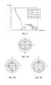
- FIG. 2 is a diagram of the voltage standing wave ratio of the dual band printed antenna in an embodiment of the present invention
- FIGS. 3A-3C are the radiation patterns of the dual band printed antenna on the X-Y plane, X-Z plane and the Y-Z plane respectively in an embodiment of the present invention
- FIG. 4A is a diagram of a top view of a dual band printed antenna in an embodiment of the present invention.
- FIG. 4B is a diagram of a bottom view of the dual band printed antenna in FIG. 4A in an embodiment of the present invention.
- FIG. 4C is a diagram of cross-sectional view of the dual band printed antenna along a direction A in FIG. 4A in an embodiment of the present invention.
- FIG. 5 is a diagram of the voltage standing wave ratio of the dual band printed antenna in an embodiment of the present invention.
- FIGS. 6A-6C are the radiation patterns of the dual band printed antenna on the X-Y plane, X-Z plane and the Y-Z plane respectively in an embodiment of the present invention
- FIG. 7A is a diagram of a top view of a dual band printed antenna in an embodiment of the present invention.
- FIG. 7B is a diagram of a bottom view of the dual band printed antenna in FIG. 1A in an embodiment of the present invention.
- FIG. 7C is a diagram of cross-sectional view of the dual band printed antenna along a direction A in FIG. 7A in an embodiment of the present invention.
- FIG. 8 is a diagram of the voltage standing wave ratio of the dual band printed antenna in an embodiment of the present invention.
- FIGS. 9A-9C are the radiation patterns of the dual band printed antenna on the X-Y plane, X-Z plane and the Y-Z plane respectively in an embodiment of the present invention.
- FIG. 10A is a diagram of a top view of a dual band printed antenna in an embodiment of the present invention.
- FIG. 10B is a diagram of a bottom view of the dual band printed antenna in FIG. 10A in an embodiment of the present invention.
- FIG. 10C is a diagram of cross-sectional view of the dual band printed antenna along a direction A in FIG. 10A in an embodiment of the present invention.
- FIG. 11 is a diagram of the voltage standing wave ratio of the dual band printed antenna in an embodiment of the present invention.
- FIGS. 12A-12C are the radiation patterns of the dual band printed antenna on the X-Y plane, X-Z plane and the Y-Z plane respectively in an embodiment of the present invention.
- FIG. 13 is a diagram illustrating average antenna gains under different frequencies when different forms of slots and antenna elements are included in the dual band printed antenna in an embodiment of the present invention.
- electrically connected or “coupled” may refer to two or more elements are in direct physical or electrical contact as, or as a solid or indirect mutual electrical contact, and the “power connection” can also refer to two or more elements are in operation or action.
- the term on the “approximately”, “about” etc., to any number of modifications or errors can change slightly, but a slight change or error does not change its nature.
- such terms of the modified micro-scope changes or errors in some embodiments be 20%, in some embodiments, may be 10%, and in some embodiments may be 5% or some other value.
- FIG. 1A is a diagram of a top view of a dual band printed antenna 1 in an embodiment of the present invention.
- FIG. 1B is a diagram of a bottom view of the dual band printed antenna 1 in FIG. 1A in an embodiment of the present invention.
- FIG. 1C is a diagram of cross-sectional view of the dual band printed antenna 1 along a direction A in FIG. 1A in an embodiment of the present invention.
- the dual band printed antenna 1 includes a metal substrate 100 , an electrically isolated supporting element 102 and a monopole antenna element 104 .
- the metal substrate 100 includes a slot 101 penetrating through two sides of the metal substrate 100 .
- the slot 101 stretches along a specific direction, in which the specific direction is X direction.
- the present invention is not limited thereto.
- the slot 101 is a close slot. More specifically, the two terminals of the slot 101 are within the metal substrate 100 .
- the slot 101 is apart from two edges of the metal substrate 100 by D 1 and D 2 , in which D 1 and D 2 are 9 millimeters and 15 millimeters respectively.
- D 1 and D 2 are 9 millimeters and 15 millimeters respectively.
- the present invention is not limited thereto.
- the electrically isolated supporting element 102 is formed on the metal substrate 100 .
- the electrically isolated supporting element 102 covers the slot 101 .
- the electrically isolated supporting element 102 may partially cover the slot 101 .
- the electrically isolated supporting element 102 includes an electrically isolated supporting layer 103 A and a circuit board layer 103 B adjacent to each other.
- a side of the electrically isolated supporting layer 103 A is disposed on the metal substrate 100 and the circuit board 103 B is disposed at another side of the electrically isolated supporting layer 103 A opposite to the metal substrate 100 such that the monopole antenna element 104 is disposed at a side of the circuit board layer 103 B opposite to the electrically isolated supporting layer 103 A.
- the thicknesses of the electrically isolated supporting layer 103 A and the circuit board 103 B can be 1 millimeter and 0.4 millimeters respectively.
- the present invention is not limited thereto.
- the monopole antenna element 104 is formed on the electrically isolated supporting layer 103 A corresponding to the position of the slot 101 .
- the monopole antenna element 104 includes a radiation part 105 and a ground part 107 .
- the radiation part 105 includes a feed point F.
- the ground part 107 is separated from the radiation part 105 for a distance. In an embodiment, both the radiation part 105 and the ground part 107 stretch along the specific direction. However, the present invention is not limited thereto.
- the dual band printed antenna 1 further includes a metal ground element 106 to be electrically coupled to the ground part 107 and the metal substrate 100 to aid the ground part 107 to be grounded.
- the metal ground element 106 can be such as, but not limited to a copper foil.
- the monopole antenna element 104 of the dual band printed antenna 1 can be driven to be in operation by disposing a transmission line (not illustrated) that includes a positive terminal electrically coupled to the feed point F and a negative terminal electrically coupled to the metal ground element 106 further to the ground.
- a transmission line (not illustrated) that includes a positive terminal electrically coupled to the feed point F and a negative terminal electrically coupled to the metal ground element 106 further to the ground.
- the radiation part 105 When the monopole antenna element 104 is in operation, the radiation part 105 resonates with the slot 101 to generate a first radiation pattern of a first frequency band and the radiation part 105 resonates itself to generate a second radiation pattern of a second frequency band.
- the first frequency band has a resonant frequency of 2.4 GHz and the second frequency band has a resonant frequency of 5 GHz. More specifically, in an embodiment, the range of the first frequency band is around 2.4 GHz to 2.5 GHz. The range of the second frequency band is around 5.15 GHz to 5.875 GHz. However, the present invention is not limited thereto.
- the size of the slot 101 may include a length of 45 millimeters and a width of 2 millimeters. However, the present invention is not limited thereto.
- a first terminal P 1 and a second terminal P 2 of the radiation part 105 are apart from the two terminals of the slot 101 by a length c and a length d that is larger than the length c.
- the feed point F is apart from the first terminal P 1 and the second terminal P 2 by a length a and a length b respectively.
- the resonant frequencies of the monopole antenna element 104 in the first frequency band and the second frequency band and the corresponding impedance matching can be adjusted by adjusting the lengths described above.
- the resonant frequency of the first frequency band can be adjusted by adjusting the lengths c and b.
- the impedance matching of the first frequency band can be adjusted by adjusting the length a.
- the resonant frequency of the second frequency band can be adjusted by adjusting the lengths c and b.
- the impedance matching of the second frequency band can be adjusted by adjusting the length b.
- FIG. 2 is a diagram of the voltage standing wave ratio (VSWR) of the dual band printed antenna 1 in an embodiment of the present invention.
- the X-axis of the diagram stands for the frequency (unit: GHz) and the Y-axis of the diagram stands for the VSWR.
- FIGS. 3A-3C are the radiation patterns of the dual band printed antenna 1 on the X-Y plane, X-Z plane and the Y-Z plane respectively in an embodiment of the present invention.
- the curves illustrated in thick lines are the radiation patterns of the first frequency band (2.4 GHz to 2.5 GHz) and the curves illustrated in dashed lines are the radiation patterns of the second frequency band (5.15 GHz to 5.875 GHz).
- the dual band printed antenna 1 has good VSWR performances in the first frequency band and the second frequency band. As illustrated in FIGS. 3A-3C , each of the radiation patterns of the dual band printed antenna 1 on each of planes is even.
- the dual band printed antenna 1 can produce two resonant frequency bands by using the coupling of the slot 101 having a shape of a single direction and the monopole antenna element 104 .
- the design of the slot is simplified, the structural strength and the appearance of the metal substrate 100 can be improved and the required signal transmission quality can be satisfied.
- the metal substrate 400 includes a slot 401 penetrating through two sides of the metal substrate 400 .
- the slot 401 stretches along a specific direction, in which the specific direction is X direction.
- the present invention is not limited thereto.
- the slot 401 is an open slot. More specifically, the metal substrate 400 includes an open terminal that is open at an edge of the metal substrate 400 and a close terminal within the metal substrate 400 .
- the slot 401 is apart from one edge of the metal substrate 400 by D 1 , in which D 1 is 9 millimeters.
- D 1 is 9 millimeters.
- the present invention is not limited thereto.
- the electrically isolated supporting element 402 is formed on the metal substrate 400 .
- the structure of the electrically isolated supporting element 402 is identical to the electrically isolated supporting element 102 illustrated in FIGS. 1A-1C . As a result, the detail thereof is not described herein.
- the monopole antenna element 404 is formed on a side of the electrically isolated supporting element 402 opposite to the metal substrate 400 corresponding to the position of the slot 401 .
- the monopole antenna element 404 includes a radiation part 405 and a ground part 407 .
- the ground part 407 can be grounded through the metal ground element 406 .
- the structure and the operation of the radiation part 405 and the ground part 407 are identical to the radiation part 105 and the ground part 107 illustrated in FIGS. 1A-1C . More specifically, the radiation part 405 resonates with the slot 401 to generate a first radiation pattern of a first frequency band and the radiation part 405 resonates itself to generate a second radiation pattern of a second frequency band. As a result, the detail thereof is not described herein.
- the first frequency band has a resonant frequency of 2.4 GHz and the second frequency band has a resonant frequency of 5 GHz. More specifically, in an embodiment, the range of the first frequency band is around 2.4 GHz to 2.5 GHz. The range of the second frequency band is around 5.15 GHz to 5.875 GHz. However, the present invention is not limited thereto.
- the size of the slot 101 may include a length of 20 millimeters and a width of 2 millimeters. However, the present invention is not limited thereto.
- a first terminal P 1 and a second terminal P 2 of the radiation part 405 are apart from the close terminal and the open terminal of the slot 401 by a length d and a length c.
- the feed point F is apart from the first terminal P 1 and the second terminal P 2 by a length a and a length b respectively.
- the resonant frequencies of the monopole antenna element 404 in the first frequency band and the second frequency band and the corresponding impedance matching can be adjusted by adjusting the lengths described above.
- the resonant frequency of the first frequency band can be adjusted by adjusting the lengths c and a.
- the impedance matching of the first frequency band can be adjusted by adjusting the length b.
- the resonant frequency of the second frequency band can be adjusted by adjusting the lengths c and a.
- the impedance matching of the second frequency band can be adjusted by adjusting the length b.
- FIG. 5 is a diagram of the voltage standing wave ratio (VSWR) of the dual band printed antenna 4 in an embodiment of the present invention.
- the X-axis of the diagram stands for the frequency (unit: GHz) and the Y-axis of the diagram stands for the VSWR.
- FIGS. 6A-6C are the radiation patterns of the dual band printed antenna 4 on the X-Y plane, X-Z plane and the Y-Z plane respectively in an embodiment of the present invention.
- the curves illustrated in thick lines are the radiation patterns of the first frequency band (2.4 GHz to 2.5 GHz) and the curves illustrated in dashed lines are the radiation patterns of the second frequency band (5.15 GHz to 5.875 GHz).
- the dual band printed antenna 1 has good VSWR performances in the first frequency band and the second frequency band. As illustrated in FIGS. 6A-6C , each of the radiation patterns of the dual band printed antenna 1 on each of planes is even.
- the dual band printed antenna 4 can produce two resonant frequency bands by using the coupling of the slot 401 having a shape of a single direction and the monopole antenna element 404 .
- the design of the slot is simplified, the structural strength and the appearance of the metal substrate 400 can be improved and the required signal transmission quality can be satisfied.
- FIG. 7A is a diagram of a top view of a dual band printed antenna 7 in an embodiment of the present invention.
- FIG. 7B is a diagram of a bottom view of the dual band printed antenna 7 in FIG. 7A in an embodiment of the present invention.
- FIG. 7C is a diagram of cross-sectional view of the dual band printed antenna 7 along a direction A in FIG. 7A in an embodiment of the present invention.
- the dual band printed antenna 7 includes a metal substrate 700 , an electrically isolated supporting element 702 and an inverted-F antenna element 704 .
- the metal substrate 700 includes a slot 701 penetrating through two sides of the metal substrate 100 .
- the slot 701 stretches along a specific direction, in which the specific direction is X direction.
- the present invention is not limited thereto.
- the slot 701 is a close slot. More specifically, the two terminals of the slot 701 are within the metal substrate 100 .
- the slot 701 is apart from two edges of the metal substrate 700 by D 1 and D 2 , in which D 1 and D 2 are 9 millimeters and 15 millimeters respectively.
- D 1 and D 2 are 9 millimeters and 15 millimeters respectively.
- the present invention is not limited thereto.
- the electrically isolated supporting element 702 is formed on the metal substrate 700 .
- the structure of the electrically isolated supporting element 702 is identical to the electrically isolated supporting element 102 illustrated in FIGS. 1A-1C . As a result, the detail thereof is not described herein.
- the inverted-F antenna element 704 includes a first radiation part 705 A, a second radiation part 705 B, a third radiation part 705 C and connection radiation parts 705 D and 705 E.
- the first radiation part 705 A stretches along the specific direction and includes a feed point F.
- the second radiation part 705 B stretches along the specific direction, is disposed at a first side of the first radiation part 705 A, is parallel and adjacent to the first radiation part 705 A and is apart from the first radiation part 705 A by a first distance.
- the third radiation part 705 C stretches along the specific direction, is disposed at a second side of the first radiation part 705 A, is parallel and adjacent to the first radiation part 705 A and is apart from the first radiation part 705 A by a second distance.
- the connection radiation part 705 D electrically couples a terminal of the second radiation part 705 B to the first radiation part 705 A and the connection radiation part 705 E electrically couples the other terminal of the second radiation part 705 B to the third radiation part 7
- the dual band printed antenna 7 further includes a metal ground element 706 to electrically couple to a part of the second radiation part 705 B serving as a ground point to electrically couple the second radiation part 705 B to the metal substrate 100 to aid the second radiation part 705 B to be grounded.
- the metal ground element 706 can be such as, but not limited to a copper foil.
- the first radiation part 705 A, the second radiation part 705 B, the third radiation part 705 C resonate with the slot 701 to generate a first radiation pattern of a first frequency band and the first radiation part 705 A, the second radiation part 705 B, the third radiation part 705 C resonate themselves to generate a second radiation pattern of a second frequency band.
- the first frequency band has a resonant frequency of 2.4 GHz and the second frequency band has a resonant frequency of 5 GHz. More specifically, in an embodiment, the range of the first frequency band is around 2.4 GHz to 2.5 GHz. The range of the second frequency band is around 5.15 GHz to 5.875 GHz. However, the present invention is not limited thereto.
- the size of the slot 701 may include a length of 45 millimeters and a width of 2 millimeters. However, the present invention is not limited thereto.
- a first terminal P 1 and a second terminal P 2 of the first radiation part 705 A are apart from the two terminals of the slot 701 by a length c and a length e that is smaller than the length c.
- the feed point F is apart from the first terminal P 1 and the second terminal P 2 by a length d and a length b respectively.
- the third radiation part 705 C has a length a.
- the resonant frequencies of the inverted-F antenna element 704 in the first frequency band and the second frequency band and the corresponding impedance matching can be adjusted by adjusting the lengths described above.
- the resonant frequency of the first frequency band can be adjusted by adjusting the lengths c and a.
- the impedance matching of the first frequency band can be adjusted by adjusting the lengths d and b.
- the resonant frequency of the second frequency band can be adjusted by adjusting the lengths c and d.
- the impedance matching of the second frequency band can be adjusted by adjusting the length b.
- FIG. 8 is a diagram of the voltage standing wave ratio (VSWR) of the dual band printed antenna 7 in an embodiment of the present invention.
- the X-axis of the diagram stands for the frequency (unit: GHz) and the Y-axis of the diagram stands for the VSWR.
- FIGS. 9A-9C are the radiation patterns of the dual band printed antenna 7 on the X-Y plane, X-Z plane and the Y-Z plane respectively in an embodiment of the present invention.
- the curves illustrated in thick lines are the radiation patterns of the first frequency band (2.4 GHz to 2.5 GHz) and the curves illustrated in dashed lines are the radiation patterns of the second frequency band (5.15 GHz to 5.875 GHz).
- the dual band printed antenna 7 has good VSWR performances in the first frequency band and the second frequency band. As illustrated in FIGS. 9A-9C , each of the radiation patterns of the dual band printed antenna 7 on each of planes is even.
- the dual band printed antenna 7 can produce two resonant frequency bands by using the coupling of the slot 701 having a shape of a single direction and the inverted-F antenna element 704 .
- the design of the slot is simplified, the structural strength and the appearance of the metal substrate 700 can be improved and the required signal transmission quality can be satisfied.
- FIG. 10A is a diagram of a top view of a dual band printed antenna 10 in an embodiment of the present invention.
- FIG. 10B is a diagram of a bottom view of the dual band printed antenna 10 in FIG. 10A in an embodiment of the present invention.
- FIG. 10C is a diagram of cross-sectional view of the dual band printed antenna 10 along a direction A in FIG. 10A in an embodiment of the present invention.
- the dual band printed antenna 10 includes a metal substrate 1000 , an electrically isolated supporting element 1002 and an inverted-F antenna element 1004 .
- the metal substrate 1000 includes a slot 1001 penetrating through two sides of the metal substrate 1000 .
- the slot 1001 stretches along a specific direction, in which the specific direction is X direction.
- the slot 1001 is an open slot. More specifically, the metal substrate 1000 includes an open terminal that is open at an edge of the metal substrate 1000 and a close terminal within the metal substrate 1000 .
- the slot 1001 is apart from one edge of the metal substrate 1000 by D 1 , in which D 1 is 9 millimeters.
- D 1 is 9 millimeters.
- the present invention is not limited thereto.
- the electrically isolated supporting element 1002 is formed on the metal substrate 1000 .
- the structure of the electrically isolated supporting element 1002 is identical to the electrically isolated supporting element 102 illustrated in FIGS. 1A-1C . As a result, the detail thereof is not described herein.
- the inverted-F antenna element 1004 includes a first radiation part 1005 A, a second radiation part 1005 B, a third radiation part 1005 C and connection radiation parts 1005 D and 1005 E.
- the second radiation part 1005 B can also be grounded by using the metal ground element 1006 .
- the structure and operation of the first radiation part 1005 A, the second radiation part 1005 B, the third radiation part 1005 C and the connection radiation parts 1005 D and 1005 E are identical the first radiation part 705 A, the second radiation part 705 B, the third radiation part 705 C and the connection radiation parts 705 D and 705 E illustrated in FIGS. 7A-7C . More specifically, the first radiation part 1005 A, the second radiation part 1005 B, the third radiation part 1005 C resonate with the slot 1001 to generate a first radiation pattern of a first frequency band and the first radiation part 1005 A, the second radiation part 1005 B, the third radiation part 1005 C resonate themselves to generate a second radiation pattern of a second frequency band. As a result, the detail thereof is not described herein.
- the first frequency band has a resonant frequency of 2.4 GHz and the second frequency band has a resonant frequency of 5 GHz. More specifically, in an embodiment, the range of the first frequency band is around 2.4 GHz to 2.5 GHz. The range of the second frequency band is around 5.15 GHz to 5.875 GHz. However, the present invention is not limited thereto.
- the size of the slot 1001 may include a length of 20 millimeters and a width of 2 millimeters. However, the present invention is not limited thereto.
- a first terminal P 1 of the first radiation part 1005 A is apart from the open terminal of the slot 1001 by a length c.
- the feed point F is apart from the first terminal P 1 and the second terminal by a length d and a length b respectively.
- the third radiation part 1005 C has a length a.
- the resonant frequencies of the inverted-F antenna element 1004 in the first frequency band and the second frequency band and the corresponding impedance matching can be adjusted by adjusting the lengths described above.
- the resonant frequency of the first frequency band can be adjusted by adjusting the lengths c and a.
- the impedance matching of the first frequency band can be adjusted by adjusting the lengths b and d.
- the resonant frequency of the second frequency band can be adjusted by adjusting the lengths c and d.
- the impedance matching of the second frequency band can be adjusted by adjusting the length b.
- FIG. 11 is a diagram of the voltage standing wave ratio (VSWR) of the dual band printed antenna 10 in an embodiment of the present invention.
- the X-axis of the diagram stands for the frequency (unit: GHz) and the Y-axis of the diagram stands for the VSWR.
- FIGS. 12A-12C are the radiation patterns of the dual band printed antenna 10 on the X-Y plane, X-Z plane and the Y-Z plane respectively in an embodiment of the present invention.
- the curves illustrated in thick lines are the radiation patterns of the first frequency band (2.4 GHz to 2.5 GHz) and the curves illustrated in dashed lines are the radiation patterns of the second frequency band (5.15 GHz to 5.875 GHz).
- the dual band printed antenna 10 has good VSWR performances in the first frequency band and the second frequency band. As illustrated in FIGS. 12A-12C , each of the radiation patterns of the dual band printed antenna 10 on each of planes is even.
- the dual band printed antenna 10 can produce two resonant frequency bands by using the coupling of the slot 1001 having a shape of a single direction and the inverted-F antenna element 1004 .
- the design of the slot is simplified, the structural strength and the appearance of the metal substrate 700 can be improved and the required signal transmission quality can be satisfied.
- FIG. 13 is a diagram illustrating average antenna gains under different frequencies when different forms of slots and antenna elements are included in the dual band printed antenna in an embodiment of the present invention.
- the average antenna gains described above is generated when a coaxial transmission line having an impedance of 50 ohms, a core diameter of 1.13 millimeters and a length of 500 millimeters is used.
- the antenna efficiency corresponding to the resonant frequency 2.4 of GHz is ⁇ 2.9 dB to ⁇ 5.1 dB.
- the antenna efficiency corresponding to the resonant frequency 5 of GHz is ⁇ 3.7 dB to ⁇ 6.2 dB.
- the antenna efficiency corresponding to the resonant frequency 2.4 of GHz is ⁇ 2.1 dB to ⁇ 2.6 dB.
- the antenna efficiency corresponding to the resonant frequency 5 of GHz is ⁇ 4.6 dB to ⁇ 5.2 dB.
- the antenna efficiency corresponding to the resonant frequency 2.4 of GHz is ⁇ 2.9 dB to ⁇ 3.4 dB.
- the antenna efficiency corresponding to the resonant frequency 5 of GHz is ⁇ 3.5 dB to ⁇ 5.5 dB.
- the antenna efficiency corresponding to the resonant frequency 2.4 of GHz is ⁇ 2.2 dB to ⁇ 2.5 dB.
- the antenna efficiency corresponding to the resonant frequency 5 of GHz is ⁇ 4.1 dB to ⁇ 5.8 dB.
- the dual band printed antenna has a great performance in the antenna efficiency.
Landscapes
- Engineering & Computer Science (AREA)
- Computer Networks & Wireless Communication (AREA)
- Details Of Aerials (AREA)
- Waveguide Aerials (AREA)
- Variable-Direction Aerials And Aerial Arrays (AREA)
Applications Claiming Priority (3)
| Application Number | Priority Date | Filing Date | Title |
|---|---|---|---|
| TW105114435A TWI689134B (zh) | 2016-05-10 | 2016-05-10 | 雙頻印刷式天線 |
| TW105114435A | 2016-05-10 | ||
| TW105114435 | 2016-05-10 |
Publications (2)
| Publication Number | Publication Date |
|---|---|
| US20170331187A1 US20170331187A1 (en) | 2017-11-16 |
| US10211533B2 true US10211533B2 (en) | 2019-02-19 |
Family
ID=58699007
Family Applications (1)
| Application Number | Title | Priority Date | Filing Date |
|---|---|---|---|
| US15/487,445 Active 2037-04-26 US10211533B2 (en) | 2016-05-10 | 2017-04-14 | Dual band printed antenna |
Country Status (4)
| Country | Link |
|---|---|
| US (1) | US10211533B2 (de) |
| EP (1) | EP3244482B1 (de) |
| CN (2) | CN110649386B (de) |
| TW (1) | TWI689134B (de) |
Cited By (2)
| Publication number | Priority date | Publication date | Assignee | Title |
|---|---|---|---|---|
| US20230336502A1 (en) * | 2016-12-29 | 2023-10-19 | Oticon A/S | Wireless communication device for communicating with multiple external devices via a wireless communication unit |
| US12431626B2 (en) | 2022-07-13 | 2025-09-30 | Honor Device Co., Ltd. | Planar inverted F antenna pair and electronic device |
Families Citing this family (4)
| Publication number | Priority date | Publication date | Assignee | Title |
|---|---|---|---|---|
| CN108206326B (zh) * | 2018-02-28 | 2023-11-21 | 深圳市国质信网络通讯有限公司 | 一种插件式wifi双频天线及机顶盒 |
| CN108832300A (zh) * | 2018-06-25 | 2018-11-16 | 英华达(上海)科技有限公司 | 天线装置 |
| TWI704716B (zh) * | 2019-07-05 | 2020-09-11 | 宏碁股份有限公司 | 行動裝置 |
| CN112490648B (zh) * | 2020-11-06 | 2022-09-13 | 杭州电子科技大学 | 一种微带线的超宽带天线 |
Citations (14)
| Publication number | Priority date | Publication date | Assignee | Title |
|---|---|---|---|---|
| TW561647B (en) | 2002-05-23 | 2003-11-11 | Yageo Corp | Dual-band dual-slot antenna |
| EP1401050A1 (de) | 2002-09-19 | 2004-03-24 | Filtronic LK Oy | Interne Antenne |
| EP1831955A1 (de) | 2004-12-30 | 2007-09-12 | Fractus, S.A. | Geformte massefläche für eine funkvorrichtung |
| US7663551B2 (en) * | 2005-11-24 | 2010-02-16 | Pulse Finald Oy | Multiband antenna apparatus and methods |
| TWM397612U (en) | 2010-09-15 | 2011-02-01 | Advanced Connection Tech Inc | Portable electronic device |
| US20110260925A1 (en) * | 2010-04-23 | 2011-10-27 | Laurian Petru Chirila | Multiband internal patch antenna for mobile terminals |
| TW201218508A (en) | 2010-08-25 | 2012-05-01 | Advanced Connection Tech Inc | Antenna structure |
| CN202601846U (zh) | 2012-05-09 | 2012-12-12 | 哗裕实业股份有限公司 | 槽孔天线 |
| TW201411931A (zh) | 2012-09-07 | 2014-03-16 | Acer Inc | 行動裝置 |
| TWI487204B (zh) | 2011-06-21 | 2015-06-01 | Inventec Appliances Corp | 具調整槽道之單極槽孔天線結構 |
| US9123990B2 (en) * | 2011-10-07 | 2015-09-01 | Pulse Finland Oy | Multi-feed antenna apparatus and methods |
| US20150263430A1 (en) | 2014-03-17 | 2015-09-17 | Quanta Computer Inc. | Antenna structure |
| US20150311594A1 (en) | 2014-04-24 | 2015-10-29 | Apple Inc. | Electronic Devices With Hybrid Antennas |
| EP3113285A1 (de) | 2015-07-03 | 2017-01-04 | Acer Incorporated | Mobile vorrichtung |
Family Cites Families (9)
| Publication number | Priority date | Publication date | Assignee | Title |
|---|---|---|---|---|
| DE10210341A1 (de) * | 2002-03-08 | 2003-09-25 | Philips Intellectual Property | Mehrband-Mikrowellenantenne |
| JP2004247790A (ja) * | 2003-02-10 | 2004-09-02 | Ngk Spark Plug Co Ltd | 逆fアンテナ |
| TW562260U (en) * | 2003-03-14 | 2003-11-11 | Hon Hai Prec Ind Co Ltd | Multi-band printed monopole antenna |
| TWI341053B (en) * | 2008-08-20 | 2011-04-21 | Acer Inc | Multiband monopole slot antenna |
| TW201042817A (en) * | 2009-05-21 | 2010-12-01 | Univ Nat Sun Yat Sen | A mobile communication device |
| TW201126811A (en) * | 2010-01-27 | 2011-08-01 | Chi Mei Comm Systems Inc | Antenna module |
| US8779985B2 (en) * | 2011-08-18 | 2014-07-15 | Qualcomm Incorporated | Dual radiator monopole antenna |
| CN103633418B (zh) * | 2012-08-20 | 2016-06-08 | 富士康(昆山)电脑接插件有限公司 | 多频平面倒f型天线 |
| CN103682583B (zh) * | 2012-09-21 | 2016-12-21 | 宏碁股份有限公司 | 移动装置 |
-
2016
- 2016-05-10 TW TW105114435A patent/TWI689134B/zh active
-
2017
- 2017-04-14 US US15/487,445 patent/US10211533B2/en active Active
- 2017-05-08 CN CN201911071351.0A patent/CN110649386B/zh active Active
- 2017-05-08 CN CN201710318567.7A patent/CN107359406B/zh active Active
- 2017-05-09 EP EP17170158.4A patent/EP3244482B1/de active Active
Patent Citations (14)
| Publication number | Priority date | Publication date | Assignee | Title |
|---|---|---|---|---|
| TW561647B (en) | 2002-05-23 | 2003-11-11 | Yageo Corp | Dual-band dual-slot antenna |
| EP1401050A1 (de) | 2002-09-19 | 2004-03-24 | Filtronic LK Oy | Interne Antenne |
| EP1831955A1 (de) | 2004-12-30 | 2007-09-12 | Fractus, S.A. | Geformte massefläche für eine funkvorrichtung |
| US7663551B2 (en) * | 2005-11-24 | 2010-02-16 | Pulse Finald Oy | Multiband antenna apparatus and methods |
| US20110260925A1 (en) * | 2010-04-23 | 2011-10-27 | Laurian Petru Chirila | Multiband internal patch antenna for mobile terminals |
| TW201218508A (en) | 2010-08-25 | 2012-05-01 | Advanced Connection Tech Inc | Antenna structure |
| TWM397612U (en) | 2010-09-15 | 2011-02-01 | Advanced Connection Tech Inc | Portable electronic device |
| TWI487204B (zh) | 2011-06-21 | 2015-06-01 | Inventec Appliances Corp | 具調整槽道之單極槽孔天線結構 |
| US9123990B2 (en) * | 2011-10-07 | 2015-09-01 | Pulse Finland Oy | Multi-feed antenna apparatus and methods |
| CN202601846U (zh) | 2012-05-09 | 2012-12-12 | 哗裕实业股份有限公司 | 槽孔天线 |
| TW201411931A (zh) | 2012-09-07 | 2014-03-16 | Acer Inc | 行動裝置 |
| US20150263430A1 (en) | 2014-03-17 | 2015-09-17 | Quanta Computer Inc. | Antenna structure |
| US20150311594A1 (en) | 2014-04-24 | 2015-10-29 | Apple Inc. | Electronic Devices With Hybrid Antennas |
| EP3113285A1 (de) | 2015-07-03 | 2017-01-04 | Acer Incorporated | Mobile vorrichtung |
Cited By (3)
| Publication number | Priority date | Publication date | Assignee | Title |
|---|---|---|---|---|
| US20230336502A1 (en) * | 2016-12-29 | 2023-10-19 | Oticon A/S | Wireless communication device for communicating with multiple external devices via a wireless communication unit |
| US12177136B2 (en) * | 2016-12-29 | 2024-12-24 | Oticon A/S | Wireless communication device for communicating with multiple external devices via a wireless communication unit |
| US12431626B2 (en) | 2022-07-13 | 2025-09-30 | Honor Device Co., Ltd. | Planar inverted F antenna pair and electronic device |
Also Published As
| Publication number | Publication date |
|---|---|
| CN107359406B (zh) | 2020-04-21 |
| EP3244482A1 (de) | 2017-11-15 |
| TWI689134B (zh) | 2020-03-21 |
| TW201740615A (zh) | 2017-11-16 |
| CN110649386A (zh) | 2020-01-03 |
| CN110649386B (zh) | 2021-01-05 |
| CN107359406A (zh) | 2017-11-17 |
| EP3244482B1 (de) | 2019-10-16 |
| US20170331187A1 (en) | 2017-11-16 |
Similar Documents
| Publication | Publication Date | Title |
|---|---|---|
| US10056696B2 (en) | Antenna structure | |
| US20170331187A1 (en) | Dual band printed antenna | |
| US11145958B2 (en) | Mobile device and manufacturing method thereof | |
| TWI600210B (zh) | 多頻段天線 | |
| US8779988B2 (en) | Surface mount device multiple-band antenna module | |
| CN1578171A (zh) | 用于降低折叠式通信手持机中接地效应的装置 | |
| WO2008000175A1 (en) | Miniature balanced antenna with differential feed | |
| TW202243327A (zh) | 天線模組及電子裝置 | |
| CN103138052A (zh) | 可携式通讯装置的多频天线 | |
| WO2018154132A1 (en) | Antenna arrangement and a device comprising such an antenna arrangement | |
| US20110221638A1 (en) | Internal lc antenna for wireless communication device | |
| US10784565B2 (en) | Mobile device and antenna structure therein | |
| US11329382B1 (en) | Antenna structure | |
| US20170317412A1 (en) | Electronic apparatus and dual band printed antenna of the same | |
| JP2003347835A (ja) | アンテナ構造およびそれを備えた通信機 | |
| US9570800B2 (en) | Ground antenna and ground radiator using capacitor | |
| US8059042B2 (en) | Shorted monopole antenna | |
| TWI509892B (zh) | 天線結構及其製造方法 | |
| CN117673743B (zh) | 一种电子设备 | |
| JP6865072B2 (ja) | アンテナ装置及びアンテナ装置を備えた電子機器 | |
| CN100470929C (zh) | 低旁瓣双频暨宽频平面型端射天线 | |
| EP4307481A1 (de) | Antenne | |
| CN115207632B (zh) | 电子装置与天线馈入模块 | |
| TWI506857B (zh) | 應用於射頻檢測程序之印刷式天線模組 | |
| CN117673708A (zh) | 一种电子设备 |
Legal Events
| Date | Code | Title | Description |
|---|---|---|---|
| AS | Assignment |
Owner name: PEGATRON CORPORATION, TAIWAN Free format text: ASSIGNMENT OF ASSIGNORS INTEREST;ASSIGNORS:HUANG, CHUN-YEN;LEE, I-SHU;YU, HUNG-MING;REEL/FRAME:042022/0891 Effective date: 20170406 |
|
| STCF | Information on status: patent grant |
Free format text: PATENTED CASE |
|
| MAFP | Maintenance fee payment |
Free format text: PAYMENT OF MAINTENANCE FEE, 4TH YEAR, LARGE ENTITY (ORIGINAL EVENT CODE: M1551); ENTITY STATUS OF PATENT OWNER: LARGE ENTITY Year of fee payment: 4 |