EP3244482B1 - Gedruckte dualbandantenne - Google Patents
Gedruckte dualbandantenne Download PDFInfo
- Publication number
- EP3244482B1 EP3244482B1 EP17170158.4A EP17170158A EP3244482B1 EP 3244482 B1 EP3244482 B1 EP 3244482B1 EP 17170158 A EP17170158 A EP 17170158A EP 3244482 B1 EP3244482 B1 EP 3244482B1
- Authority
- EP
- European Patent Office
- Prior art keywords
- radiation part
- length
- electrically isolated
- slot
- metal substrate
- Prior art date
- Legal status (The legal status is an assumption and is not a legal conclusion. Google has not performed a legal analysis and makes no representation as to the accuracy of the status listed.)
- Active
Links
Images




Classifications
-
- H—ELECTRICITY
- H01—ELECTRIC ELEMENTS
- H01Q—ANTENNAS, i.e. RADIO AERIALS
- H01Q5/00—Arrangements for simultaneous operation of antennas on two or more different wavebands, e.g. dual-band or multi-band arrangements
- H01Q5/30—Arrangements for providing operation on different wavebands
- H01Q5/307—Individual or coupled radiating elements, each element being fed in an unspecified way
- H01Q5/314—Individual or coupled radiating elements, each element being fed in an unspecified way using frequency dependent circuits or components, e.g. trap circuits or capacitors
- H01Q5/328—Individual or coupled radiating elements, each element being fed in an unspecified way using frequency dependent circuits or components, e.g. trap circuits or capacitors between a radiating element and ground
-
- H—ELECTRICITY
- H01—ELECTRIC ELEMENTS
- H01Q—ANTENNAS, i.e. RADIO AERIALS
- H01Q1/00—Details of, or arrangements associated with, antennas
- H01Q1/12—Supports; Mounting means
- H01Q1/22—Supports; Mounting means by structural association with other equipment or articles
- H01Q1/2291—Supports; Mounting means by structural association with other equipment or articles used in Bluetooth® or Wi-Fi® devices of Wireless Local Area Networks [WLAN]
-
- H—ELECTRICITY
- H01—ELECTRIC ELEMENTS
- H01Q—ANTENNAS, i.e. RADIO AERIALS
- H01Q1/00—Details of, or arrangements associated with, antennas
- H01Q1/36—Structural form of radiating elements, e.g. cone, spiral, umbrella; Particular materials used therewith
- H01Q1/38—Structural form of radiating elements, e.g. cone, spiral, umbrella; Particular materials used therewith formed by a conductive layer on an insulating support
-
- H—ELECTRICITY
- H01—ELECTRIC ELEMENTS
- H01Q—ANTENNAS, i.e. RADIO AERIALS
- H01Q1/00—Details of, or arrangements associated with, antennas
- H01Q1/48—Earthing means; Earth screens; Counterpoises
-
- H—ELECTRICITY
- H01—ELECTRIC ELEMENTS
- H01Q—ANTENNAS, i.e. RADIO AERIALS
- H01Q1/00—Details of, or arrangements associated with, antennas
- H01Q1/50—Structural association of antennas with earthing switches, lead-in devices or lightning protectors
-
- H—ELECTRICITY
- H01—ELECTRIC ELEMENTS
- H01Q—ANTENNAS, i.e. RADIO AERIALS
- H01Q13/00—Waveguide horns or mouths; Slot antennas; Leaky-waveguide antennas; Equivalent structures causing radiation along the transmission path of a guided wave
- H01Q13/10—Resonant slot antennas
- H01Q13/106—Microstrip slot antennas
-
- H—ELECTRICITY
- H01—ELECTRIC ELEMENTS
- H01Q—ANTENNAS, i.e. RADIO AERIALS
- H01Q5/00—Arrangements for simultaneous operation of antennas on two or more different wavebands, e.g. dual-band or multi-band arrangements
- H01Q5/20—Arrangements for simultaneous operation of antennas on two or more different wavebands, e.g. dual-band or multi-band arrangements characterised by the operating wavebands
-
- H—ELECTRICITY
- H01—ELECTRIC ELEMENTS
- H01Q—ANTENNAS, i.e. RADIO AERIALS
- H01Q5/00—Arrangements for simultaneous operation of antennas on two or more different wavebands, e.g. dual-band or multi-band arrangements
- H01Q5/30—Arrangements for providing operation on different wavebands
- H01Q5/307—Individual or coupled radiating elements, each element being fed in an unspecified way
- H01Q5/314—Individual or coupled radiating elements, each element being fed in an unspecified way using frequency dependent circuits or components, e.g. trap circuits or capacitors
- H01Q5/335—Individual or coupled radiating elements, each element being fed in an unspecified way using frequency dependent circuits or components, e.g. trap circuits or capacitors at the feed, e.g. for impedance matching
-
- H—ELECTRICITY
- H01—ELECTRIC ELEMENTS
- H01Q—ANTENNAS, i.e. RADIO AERIALS
- H01Q5/00—Arrangements for simultaneous operation of antennas on two or more different wavebands, e.g. dual-band or multi-band arrangements
- H01Q5/30—Arrangements for providing operation on different wavebands
- H01Q5/378—Combination of fed elements with parasitic elements
-
- H—ELECTRICITY
- H01—ELECTRIC ELEMENTS
- H01Q—ANTENNAS, i.e. RADIO AERIALS
- H01Q9/00—Electrically-short antennas having dimensions not more than twice the operating wavelength and consisting of conductive active radiating elements
- H01Q9/04—Resonant antennas
- H01Q9/0407—Substantially flat resonant element parallel to ground plane, e.g. patch antenna
- H01Q9/0421—Substantially flat resonant element parallel to ground plane, e.g. patch antenna with a shorting wall or a shorting pin at one end of the element
-
- H—ELECTRICITY
- H01—ELECTRIC ELEMENTS
- H01Q—ANTENNAS, i.e. RADIO AERIALS
- H01Q9/00—Electrically-short antennas having dimensions not more than twice the operating wavelength and consisting of conductive active radiating elements
- H01Q9/04—Resonant antennas
- H01Q9/0407—Substantially flat resonant element parallel to ground plane, e.g. patch antenna
- H01Q9/0442—Substantially flat resonant element parallel to ground plane, e.g. patch antenna with particular tuning means
-
- H—ELECTRICITY
- H01—ELECTRIC ELEMENTS
- H01Q—ANTENNAS, i.e. RADIO AERIALS
- H01Q9/00—Electrically-short antennas having dimensions not more than twice the operating wavelength and consisting of conductive active radiating elements
- H01Q9/04—Resonant antennas
- H01Q9/30—Resonant antennas with feed to end of elongated active element, e.g. unipole
Definitions
- the present invention relates to an antenna technology. More particularly, the present invention relates to a dual band printed antenna.
- Document EP 3113285 A1 provides a mobile device with a novel antenna structure.
- Document EP 1831955 A1 provides an antenna structure for a wireless device comprising a ground plane and an antenna element.
- Document US 20150311594 A1 provides an electronic device with hybrid planar inverted-F slot antennas and indirectly fed slot antennas.
- Document EP 1401050 A1 provides an internal planar antenna for small radio apparatuses. In general, in order to shrink the volume of the electronic communication devices, most manufacturers make improvement on the printed antenna. However, not only the adjustment and control of operation frequencies need to be taken into consideration when the electronic communication devices are modified to make improvement, but also the human resource cost spent during the manufacturing process is needed to be evaluated.
- the invention provides a dual band printed antenna that includes a metal substrate, an electrically isolated supporting element and a monopole antenna element.
- the metal substrate includes a slot.
- a side of the electrically isolated supporting element is formed on the metal substrate.
- the monopole antenna element is formed on the other side of the electrically isolated supporting element and corresponding to the position of the slot, and the monopole antenna element includes a radiation part and a ground part.
- the radiation part includes a feed point.
- the ground part is separated from the radiation part for a distance.
- the radiation part resonates with the slot to generate a first radiation pattern of a first frequency band and the radiation part resonates itself to generate a second radiation pattern of a second frequency band.
- Another aspect of the present invention is to provide a dual band printed antenna that includes a metal substrate, an electrically isolated supporting element and an inverted-F antenna element.
- the metal substrate includes a slot.
- a side of the electrically isolated supporting element is formed on the metal substrate.
- the inverted-F antenna element is formed on the other side of the electrically isolated supporting element and corresponding to the position of the slot, and the inverted-F antenna element includes at least one radiation part comprising a feed point and a ground point.
- the radiation part resonates with the slot to generate a first radiation pattern of a first frequency band and the radiation part resonates itself to generate a second radiation pattern of a second frequency band.
- electrically connected or “coupled” may refer to two or more elements are in direct physical or electrical contact as, or as a solid or indirect mutual electrical contact, and the "power connection” can also refer to two or more elements are in operation or action.
- FIG. 1A is a diagram of a top view of a dual band printed antenna 1 in an embodiment of the present invention.
- FIG. 1B is a diagram of a bottom view of the dual band printed antenna 1 in FIG. 1A in an embodiment of the present invention.
- FIG. 1C is a diagram of cross-sectional view of the dual band printed antenna 1 along a direction A in FIG. 1A in an embodiment of the present invention.
- the dual band printed antenna 1 includes a metal substrate 100, an electrically isolated supporting element 102 and a monopole antenna element 104.
- the metal substrate 100 includes a slot 101 penetrating through two sides of the metal substrate 100.
- the slot 101 stretches along a specific direction, in which the specific direction is X direction.
- the present invention is not limited thereto.
- the slot 101 is a close slot. More specifically, the two terminals of the slot 101 are within the metal substrate 100.
- the slot 101 is apart from two edges of the metal substrate 100 by D1 and D2, in which D1 and D2 are 9 millimeters and 15 millimeters respectively.
- D1 and D2 are 9 millimeters and 15 millimeters respectively.
- the present invention is not limited thereto.
- the electrically isolated supporting element 102 is formed on the metal substrate 100. In an embodiment, the electrically isolated supporting element 102 covers the slot 101. In other embodiment, the electrically isolated supporting element 102 may partially cover the slot 101.
- the electrically isolated supporting element 102 includes an electrically isolated supporting layer 103A and a circuit board layer 103B adjacent to each other.
- a side of the electrically isolated supporting layer 103A is disposed on the metal substrate 100 and the circuit board 103B is disposed at another side of the electrically isolated supporting layer 103A opposite to the metal substrate 100 such that the monopole antenna element 104 is disposed at a side of the circuit board layer 103B opposite to the electrically isolated supporting layer 103A.
- the thicknesses of the electrically isolated supporting layer 103A and the circuit board 103B can be 1 millimeter and 0.4 millimeters respectively.
- the present invention is not limited thereto.
- the monopole antenna element 104 is formed on the electrically isolated supporting layer 103A corresponding to the position of the slot 101.
- the monopole antenna element 104 includes a radiation part 105 and a ground part 107.
- the radiation part 105 includes a feed point F.
- the ground part 107 is separated from the radiation part 105 for a distance. In an embodiment, both the radiation part 105 and the ground part 107 stretch along the specific direction. However, the present invention is not limited thereto.
- the dual band printed antenna 1 further includes a metal ground element 106 to be electrically coupled to the ground part 107 and the metal substrate 100 to aid the ground part 107 to be grounded.
- the metal ground element 106 can be such as, but not limited to a copper foil.
- the monopole antenna element 104 of the dual band printed antenna 1 can be driven to be in operation by disposing a transmission line (not illustrated) that includes a positive terminal electrically coupled to the feed point F and a negative terminal electrically coupled to the metal ground element 106 further to the ground.
- a transmission line (not illustrated) that includes a positive terminal electrically coupled to the feed point F and a negative terminal electrically coupled to the metal ground element 106 further to the ground.
- the radiation part 105 When the monopole antenna element 104 is in operation, the radiation part 105 resonates with the slot 101 to generate a first radiation pattern of a first frequency band and the radiation part 105 resonates itself to generate a second radiation pattern of a second frequency band.
- the first frequency band has a resonant frequency of 2.4 GHz and the second frequency band has a resonant frequency of 5 GHz. More specifically, in an embodiment, the range of the first frequency band is around 2.4 GHz to 2.5 GHz. The range of the second frequency band is around 5.15 GHz to 5.875 GHz. However, the present invention is not limited thereto.
- the size of the slot 101 may include a length of 45 millimeters and a width of 2 millimeters. However, the present invention is not limited thereto.
- a first terminal P1 and a second terminal P2 of the radiation part 105 are apart from the two terminals of the slot 101 by a length c and a length d that is larger than the length c.
- the feed point F is apart from the first terminal P1 and the second terminal P2 by a length a and a length b respectively.
- the resonant frequencies of the monopole antenna element 104 in the first frequency band and the second frequency band and the corresponding impedance matching can be adjusted by adjusting the lengths described above.
- the resonant frequency of the first frequency band can be adjusted by adjusting the lengths c and b.
- the impedance matching of the first frequency band can be adjusted by adjusting the length a.
- the resonant frequency of the second frequency band can be adjusted by adjusting the lengths c and b.
- the impedance matching of the second frequency band can be adjusted by adjusting the length b.
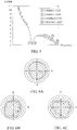
- FIG. 2 is a diagram of the voltage standing wave ratio (VSWR) of the dual band printed antenna 1 in an embodiment of the present invention.
- the X-axis of the diagram stands for the frequency (unit: GHz) and the Y-axis of the diagram stands for the VSWR.
- FIGs. 3A-3C are the radiation patterns of the dual band printed antenna 1 on the X-Y plane, X-Z plane and the Y-Z plane respectively in an embodiment of the present invention.
- the curves illustrated in thick lines are the radiation patterns of the first frequency band (2.4 GHz to 2.5 GHz) and the curves illustrated in dashed lines are the radiation patterns of the second frequency band (5.15 GHz to 5.875 GHz).
- the dual band printed antenna 1 has good VSWR performances in the first frequency band and the second frequency band. As illustrated in FIGs. 3A-3C , each of the radiation patterns of the dual band printed antenna 1 on each of planes is even.
- the dual band printed antenna 1 can produce two resonant frequency bands by using the coupling of the slot 101 having a shape of a single direction and the monopole antenna element 104.
- the design of the slot is simplified, the structural strength and the appearance of the metal substrate 100 can be improved and the required signal transmission quality can be satisfied.
- FIG. 4A is a diagram of a top view of a dual band printed antenna 4 in an embodiment of the present invention.
- FIG. 4B is a diagram of a bottom view of the dual band printed antenna 4 in FIG. 4A in an embodiment of the present invention.
- FIG. 4C is a diagram of cross-sectional view of the dual band printed antenna 4 along a direction A in FIG. 4A in an embodiment of the present invention.
- the dual band printed antenna 4 includes a metal substrate 400, an electrically isolated supporting element 402 and a monopole antenna element 404.
- the metal substrate 400 includes a slot 401 penetrating through two sides of the metal substrate 400.
- the slot 401 stretches along a specific direction, in which the specific direction is X direction.
- the present invention is not limited thereto.
- the slot 401 is an open slot. More specifically, the metal substrate 400 includes an open terminal that is open at an edge of the metal substrate 400 and a close terminal within the metal substrate 400.
- the slot 401 is apart from one edge of the metal substrate 400 by D1, in which D1 is 9 millimeters.
- D1 is 9 millimeters.
- the present invention is not limited thereto.
- the electrically isolated supporting element 402 is formed on the metal substrate 400.
- the structure of the electrically isolated supporting element 402 is identical to the electrically isolated supporting element 102 illustrated in FIGs. 1A-1C . As a result, the detail thereof is not described herein.
- the monopole antenna element 404 is formed on a side of the electrically isolated supporting element 402 opposite to the metal substrate 400 corresponding to the position of the slot 401.
- the monopole antenna element 404 includes a radiation part 405 and a ground part 407.
- the ground part 407 can be grounded through the metal ground element 406.
- the structure and the operation of the radiation part 405 and the ground part 407 are identical to the radiation part 105 and the ground part 107 illustrated in FIGs. 1A-1C . More specifically, the radiation part 405 resonates with the slot 401 to generate a first radiation pattern of a first frequency band and the radiation part 405 resonates itself to generate a second radiation pattern of a second frequency band. As a result, the detail thereof is not described herein.
- the first frequency band has a resonant frequency of 2.4 GHz and the second frequency band has a resonant frequency of 5 GHz. More specifically, in an embodiment, the range of the first frequency band is around 2.4 GHz to 2.5 GHz. The range of the second frequency band is around 5.15 GHz to 5.875 GHz. However, the present invention is not limited thereto.
- the size of the slot 101 may include a length of 20 millimeters and a width of 2 millimeters. However, the present invention is not limited thereto.
- a first terminal P1 and a second terminal P2 of the radiation part 405 are apart from the close terminal and the open terminal of the slot 401 by a length d and a length c.
- the feed point F is apart from the first terminal P1 and the second terminal P2 by a length a and a length b respectively.
- the resonant frequencies of the monopole antenna element 404 in the first frequency band and the second frequency band and the corresponding impedance matching can be adjusted by adjusting the lengths described above.
- the resonant frequency of the first frequency band can be adjusted by adjusting the lengths c and a.
- the impedance matching of the first frequency band can be adjusted by adjusting the length b.
- the resonant frequency of the second frequency band can be adjusted by adjusting the lengths c and a.
- the impedance matching of the second frequency band can be adjusted by adjusting the length b.
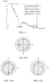
- FIG. 5 is a diagram of the voltage standing wave ratio (VSWR) of the dual band printed antenna 4 in an embodiment of the present invention.
- the X-axis of the diagram stands for the frequency (unit: GHz) and the Y-axis of the diagram stands for the VSWR.
- FIGs. 6A-6C are the radiation patterns of the dual band printed antenna 4 on the X-Y plane, X-Z plane and the Y-Z plane respectively in an embodiment of the present invention.
- the curves illustrated in thick lines are the radiation patterns of the first frequency band (2.4 GHz to 2.5 GHz) and the curves illustrated in dashed lines are the radiation patterns of the second frequency band (5.15 GHz to 5.875 GHz).
- the dual band printed antenna 1 has good VSWR performances in the first frequency band and the second frequency band. As illustrated in FIGs. 6A-6C , each of the radiation patterns of the dual band printed antenna 1 on each plane is even.
- the dual band printed antenna 4 can produce two resonant frequency bands by using the coupling of the slot 401 having a shape of a single direction and the monopole antenna element 404.
- the design of the slot is simplified, the structural strength and the appearance of the metal substrate 400 can be improved and the required signal transmission quality can be satisfied.
- FIG. 7A is a diagram of a top view of a dual band printed antenna 7 in an embodiment of the present invention.
- FIG. 7B is a diagram of a bottom view of the dual band printed antenna 7 in FIG. 7A in an embodiment of the present invention.
- FIG. 7C is a diagram of cross-sectional view of the dual band printed antenna 7 along a direction A in FIG. 7A in an embodiment of the present invention.
- the dual band printed antenna 7 includes a metal substrate 700, an electrically isolated supporting element 702 and an inverted-F antenna element 704.
- the metal substrate 700 includes a slot 701 penetrating through two sides of the metal substrate 700.
- the slot 701 stretches along a specific direction, in which the specific direction is X direction.
- the present invention is not limited thereto.
- the slot 701 is a close slot. More specifically, the two terminals of the slot 701 are within the metal substrate 700.
- the slot 701 is apart from two edges of the metal substrate 700 by D1 and D2, in which D1 and D2 are 9 millimeters and 15 millimeters respectively.
- D1 and D2 are 9 millimeters and 15 millimeters respectively.
- the present invention is not limited thereto.
- the electrically isolated supporting element 702 is formed on the metal substrate 700.
- the structure of the electrically isolated supporting element 702 is identical to the electrically isolated supporting element 102 illustrated in FIGs. 1A-1C . As a result, the detail thereof is not described herein.
- the inverted-F antenna element 704 includes a first radiation part 705A, a second radiation part 705B, a third radiation part 705C and connection radiation parts 705D and 705E.
- the first radiation part 705A stretches along the specific direction and includes a feed point F.
- the second radiation part 705B stretches along the specific direction, is disposed at a first side of the first radiation part 705A, is parallel and adjacent to the first radiation part 705A and is apart from the first radiation part 705A by a first distance.
- the third radiation part 705C stretches along the specific direction, is disposed at a second side of the first radiation part 705A, is parallel and adjacent to the first radiation part 705A and is apart from the first radiation part 705A by a second distance.
- the connection radiation part 705D electrically couples a terminal of the second radiation part 705B to the first radiation part 705A and the connection radiation part 705E electrically couples the other terminal of the second radiation part 705B to the third radiation part 7
- the dual band printed antenna 7 further includes a metal ground element 706 to electrically couple to a part of the second radiation part 705B serving as a ground point to electrically couple the second radiation part 705B to the metal substrate 100 to aid the second radiation part 705B to be grounded.
- the metal ground element 706 can be such as, but not limited to a copper foil.
- the first radiation part 705A, the second radiation part 705B, the third radiation part 705C resonate with the slot 701 to generate a first radiation pattern of a first frequency band and the first radiation part 705A, the second radiation part 705B, the third radiation part 705C resonate themselves to generate a second radiation pattern of a second frequency band.
- the first frequency band has a resonant frequency of 2.4 GHz and the second frequency band has a resonant frequency of 5 GHz. More specifically, in an embodiment, the range of the first frequency band is around 2.4 GHz to 2.5 GHz. The range of the second frequency band is around 5.15 GHz to 5.875 GHz. However, the present invention is not limited thereto.
- the size of the slot 701 may include a length of 45 millimeters and a width of 2 millimeters. However, the present invention is not limited thereto.
- a first terminal P1 and a second terminal P2 of the first radiation part 705A are apart from the two terminals of the slot 701 by a length c and a length e that is smaller than the length c.
- the feed point F is apart from the first terminal P1 and the second terminal P2 by a length d and a length b respectively.
- the third radiation part 705C has a length a. The resonant frequencies of the inverted-F antenna element 704 in the first frequency band and the second frequency band and the corresponding impedance matching can be adjusted by adjusting the lengths described above.
- the resonant frequency of the first frequency band can be adjusted by adjusting the lengths c and a.
- the impedance matching of the first frequency band can be adjusted by adjusting the lengths d and b.
- the resonant frequency of the second frequency band can be adjusted by adjusting the lengths c and d.
- the impedance matching of the second frequency band can be adjusted by adjusting the length b.
- FIG. 8 is a diagram of the voltage standing wave ratio (VSWR) of the dual band printed antenna 7 in an embodiment of the present invention.
- the X-axis of the diagram stands for the frequency (unit: GHz) and the Y-axis of the diagram stands for the VSWR.
- FIGs. 9A-9C are the radiation patterns of the dual band printed antenna 7 on the X-Y plane, X-Z plane and the Y-Z plane respectively in an embodiment of the present invention.
- the curves illustrated in thick lines are the radiation patterns of the first frequency band (2.4 GHz to 2.5 GHz) and the curves illustrated in dashed lines are the radiation patterns of the second frequency band (5.15 GHz to 5.875 GHz).
- the dual band printed antenna 7 has good VSWR performances in the first frequency band and the second frequency band. As illustrated in FIGs. 9A-9C , each of the radiation patterns of the dual band printed antenna 7 on each of planes is even.
- the dual band printed antenna 7 can produce two resonant frequency bands by using the coupling of the slot 701 having a shape of a single direction and the inverted-F antenna element 704.
- the design of the slot is simplified, the structural strength and the appearance of the metal substrate 700 can be improved and the required signal transmission quality can be satisfied.
- FIG. 10A is a diagram of a top view of a dual band printed antenna 10 in an embodiment of the present invention.
- FIG. 10B is a diagram of a bottom view of the dual band printed antenna 10 in FIG. 10A in an embodiment of the present invention.
- FIG. 10C is a diagram of cross-sectional view of the dual band printed antenna 10 along a direction A in FIG. 10A in an embodiment of the present invention.
- the dual band printed antenna 10 includes a metal substrate 1000, an electrically isolated supporting element 1002 and an inverted-F antenna element 1004.
- the metal substrate 1000 includes a slot 1001 penetrating through two sides of the metal substrate 1000.
- the slot 1001 stretches along a specific direction, in which the specific direction is X direction.
- the present invention is not limited thereto.
- the slot 1001 is an open slot. More specifically, the metal substrate 1000 includes an open terminal that is open at an edge of the metal substrate 1000 and a close terminal within the metal substrate 1000.
- the slot 1001 is apart from one edge of the metal substrate 1000 by D1, in which D1 is 9 millimeters.
- D1 is 9 millimeters.
- the present invention is not limited thereto.
- the electrically isolated supporting element 1002 is formed on the metal substrate 1000.
- the structure of the electrically isolated supporting element 1002 is identical to the electrically isolated supporting element 102 illustrated in FIGs. 1A-1C . As a result, the detail thereof is not described herein.
- the inverted-F antenna element 1004 includes a first radiation part 1005A, a second radiation part 1005B, a third radiation part 1005C and connection radiation parts 1005D and 1005E.
- the second radiation part 1005B can also be grounded by using the metal ground element 1006.
- the structure and operation of the first radiation part 1005A, the second radiation part 1005B, the third radiation part 1005C and the connection radiation parts 1005D and 1005E are identical the first radiation part 705A, the second radiation part 705B, the third radiation part 705C and the connection radiation parts 705D and 705E illustrated in FIGs. 7A-7C . More specifically, the first radiation part 1005A, the second radiation part 1005B, the third radiation part 1005C resonate with the slot 1001 to generate a first radiation pattern of a first frequency band and the first radiation part 1005A, the second radiation part 1005B, the third radiation part 1005C resonate themselves to generate a second radiation pattern of a second frequency band. As a result, the detail thereof is not described herein.
- the first frequency band has a resonant frequency of 2.4 GHz and the second frequency band has a resonant frequency of 5 GHz. More specifically, in an embodiment, the range of the first frequency band is around 2.4 GHz to 2.5 GHz. The range of the second frequency band is around 5.15 GHz to 5.875 GHz. However, the present invention is not limited thereto.
- the size of the slot 1001 may include a length of 20 millimeters and a width of 2 millimeters. However, the present invention is not limited thereto.
- a first terminal P1 of the first radiation part 1005A is apart from the open terminal of the slot 1001 by a length c.
- the feed point F is apart from the first terminal P1 and the second terminal by a length d and a length b respectively.
- the third radiation part 1005C has a length a.
- the resonant frequencies of the inverted-F antenna element 1004 in the first frequency band and the second frequency band and the corresponding impedance matching can be adjusted by adjusting the lengths described above.
- the resonant frequency of the first frequency band can be adjusted by adjusting the lengths c and a.
- the impedance matching of the first frequency band can be adjusted by adjusting the lengths b and d.
- the resonant frequency of the second frequency band can be adjusted by adjusting the lengths c and d.
- the impedance matching of the second frequency band can be adjusted by adjusting the length b.
- FIG. 11 is a diagram of the voltage standing wave ratio (VSWR) of the dual band printed antenna 10 in an embodiment of the present invention.
- the X-axis of the diagram stands for the frequency (unit: GHz) and the Y-axis of the diagram stands for the VSWR.
- FIGs. 12A-12C are the radiation patterns of the dual band printed antenna 10 on the X-Y plane, X-Z plane and the Y-Z plane respectively in an embodiment of the present invention.
- the curves illustrated in thick lines are the radiation patterns of the first frequency band (2.4 GHz to 2.5 GHz) and the curves illustrated in dashed lines are the radiation patterns of the second frequency band (5.15 GHz to 5.875 GHz).
- the dual band printed antenna 10 has good VSWR performances in the first frequency band and the second frequency band. As illustrated in FIGs. 12A-12C , each of the radiation patterns of the dual band printed antenna 10 on each of planes is even.
- the dual band printed antenna 10 can produce two resonant frequency bands by using the coupling of the slot 1001 having a shape of a single direction and the inverted-F antenna element 1004.
- the design of the slot is simplified, the structural strength and the appearance of the metal substrate 700 can be improved and the required signal transmission quality can be satisfied.
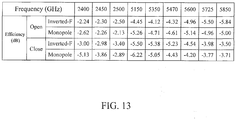
- FIG. 13 is a diagram illustrating average antenna gains under different frequencies when different forms of slots and antenna elements are included in the dual band printed antenna in an embodiment of the present invention.
- the average antenna gains described above is generated when a coaxial transmission line having an impedance of 50 ohms, a core diameter of 1.13 millimeters and a length of 500 millimeters is used.
- the antenna efficiency corresponding to the resonant frequency 2.4 of GHz is -2.9 dB to -5.1 dB.
- the antenna efficiency corresponding to the resonant frequency 5 of GHz is -3.7 dB to -6.2 dB.
- the antenna efficiency corresponding to the resonant frequency 2.4 of GHz is -2.1 dB to -2.6 dB.
- the antenna efficiency corresponding to the resonant frequency 5 of GHz is -4.6 dB to -5.2 dB.
- the antenna efficiency corresponding to the resonant frequency 2.4 of GHz is -2.9 dB to -3.4 dB.
- the antenna efficiency corresponding to the resonant frequency 5 of GHz is -3.5 dB to -5.5 dB.
- the antenna efficiency corresponding to the resonant frequency 2.4 of GHz is -2.2 dB to -2.5 dB.
- the antenna efficiency corresponding to the resonant frequency 5 of GHz is -4.1 dB to -5.8 dB.
- the dual band printed antenna has a great performance in the antenna efficiency.
Landscapes
- Engineering & Computer Science (AREA)
- Computer Networks & Wireless Communication (AREA)
- Details Of Aerials (AREA)
- Waveguide Aerials (AREA)
- Variable-Direction Aerials And Aerial Arrays (AREA)
Claims (20)
- Gedruckte Zweibandantenne (1), die ein Metallsubstrat (100) und ein elektrisch isoliertes Stützelement (102) umfasst, wobei das Metallsubstrat einen Schlitz (101) enthält, wobei eine Seite des elektrisch isolierten Stützelementes auf dem Metallsubstrat gebildet ist, dadurch gekennzeichnet, dass die gedruckte Zweibandantenne umfasst:
ein Monopolantennenelement (104), das auf der anderen Seite des elektrisch isolierten Stützelementes gebildet ist und der Position des Schlitzes entspricht, und wobei das Monopolantennenelement umfasst:einen Strahlungsteil (105), der einen Speisepunkt (F) enthält; undeinen geerdeten Teil (107), der vom Strahlungsteil durch einen Abstand getrennt ist;wobei das elektrisch isolierte Stützelement plattenförmig ist, wobei die Seite und die andere Seite des elektrisch isolierten Stützelementes die entgegengesetzten Seiten des elektrisch isolierten Stützelementes sind, wobei der Strahlungsteil dafür ausgelegt ist, mit dem Schlitz mitzuschwingen, der dafür ausgelegt ist, ein erstes Strahlungsmuster eines ersten Frequenzbandes zu erzeugen, und der Strahlungsteil dafür ausgelegt ist, mit sich selbst zu schwingen, um ein zweites Strahlungsmuster eines zweiten Frequenzbandes zu erzeugen;wobei der Schlitz sich entlang einer spezifischen Richtung (X) erstreckt, wobei zwei Enden des Schlitzes sich innerhalb des Metallsubstrates befinden;wobei der Strahlungsteil und der geerdete Teil quaderförmig sind, wobei der Strahlungsteil und der geerdete Teil sich entlang der spezifischen Richtung erstrecken, ein erstes Ende (P1) und ein zweites Ende (P2) des Strahlungsteils sind jeweils von den zwei Enden des Schlitzes durch eine erste Länge (c) und eine zweite Länge (d), die größer als die erste Länge ist, getrennt, und der Speisepunkt ist vom ersten Ende und dem zweiten Ende durch eine dritte Länge (a) bzw. eine vierte Länge (b) getrennt;wobei eine erste Resonanzfrequenz des ersten Frequenzbandes durch die erste Länge und die vierte Länge einstellbar ist, und eine erste Impedanzanpassung des Monopolantennenelementes, die dem ersten Frequenzband entspricht, ist durch die dritte Länge einstellbar;wobei eine zweite Resonanzfrequenz des zweiten Frequenzbandes durch die erste Länge und die vierte Länge einstellbar ist, und eine zweite Impedanzanpassung des Monopolantennenelementes, die dem zweiten Frequenzband entspricht, kann durch die vierte Länge eingestellt werden. - Gedruckte Zweibandantenne nach Anspruch 1, dadurch gekennzeichnet, dass der Schlitz ein rechteckiger Schlitz ist.
- Gedruckte Zweibandantenne nach Anspruch 1, dadurch gekennzeichnet, dass die Länge des Schlitzes 45 Millimeter beträgt, und die Breite des Schlitzes beträgt 2 Millimeter.
- Gedruckte Zweibandantenne nach Anspruch 1, dadurch gekennzeichnet, dass das elektrisch isolierte Stützelement eine elektrisch isolierte Stützschicht (103A) und eine Schaltplatinenschicht (103B) hat, die einander benachbart sind, die elektrisch isolierte Stützschicht befindet sich auf dem Metallsubstrat, die Schaltplatinenschicht befindet sich an einer Seite der elektrisch isolierten Stützschicht gegenüber dem Metallsubstrat, und das Monopolantennenelement befindet sich an einer Seite der Schaltplatinenschicht gegenüber der elektrisch isolierten Stützschicht.
- Gedruckte Zweibandantenne nach Anspruch 4, dadurch gekennzeichnet, dass die Dicke der elektrisch isolierten Stützschicht 1 mm beträgt, und die Dicke der Schaltplatinenschicht beträgt 0,4 Millimeter.
- Gedruckte Zweibandantenne nach Anspruch 1, dadurch gekennzeichnet, dass die gedruckte Zweibandantenne ferner ein metallisches Erdungselement (106) umfasst, das elektrisch mit dem Erdungselement und dem Metallsubstrat verbunden werden muss, um das zu erdende Erdungselement zu unterstützen.
- Gedruckte Zweibandantenne (7), die ein Metallsubstrat (700) und ein elektrisch isoliertes Stützelement (702) umfasst, wobei das Metallsubstrat einen Schlitz (701) enthält, wobei das elektrisch isolierte Stützelement auf einer Seite des Metallsubstrats gebildet ist, dadurch gekennzeichnet, dass die gedruckte Zweibandantenne umfasst:ein umgekehrtes F-Antennenelement (704), das auf der anderen Seite des elektrisch isolierten Stützelementes gebildet ist und der Position des Schlitzes entspricht, und das umgekehrte F-Antennenelement umfasst mindestens einen Strahlungsteil (705A, 705B, 705C, 705D, 705E), der einen Speisepunkt (F) und einen Erdungspunkt umfasst;wobei das elektrisch isolierte Stützelement plattenförmig ist, wobei der Strahlungsteil dafür ausgelegt ist, mit dem Schlitz mitzuschwingen, der dafür ausgelegt ist, ein erstes Strahlungsmuster eines ersten Frequenzbandes zu erzeugen, und der Strahlungsteil ist dafür ausgelegt, mit sich selbst zu schwingen, um ein zweites Strahlungsmuster eines zweiten Frequenzbandes zu erzeugen;wobei der Schlitz sich entlang einer spezifischen Richtung (X) erstreckt, wobei zwei Enden des Schlitzes sich innerhalb des Metallsubstrates befinden;wobei die umgekehrte F-Antenne ferner einen ersten Strahlungsteil (705A) umfasst, der sich entlang der spezifischen Richtung erstreckt und den Speisepunkt enthält, wobei der erste Strahlungsteil quaderförmig ist;wobei die umgekehrte F-Antenne ferner einen dritten Strahlungsteil (705C) umfasst, der sich entlang der spezifischen Richtung erstreckt, wobei der dritte Strahlungsteil quaderförmig ist und an einer zweiten Seite des ersten Strahlungsteils angeordnet ist, wobei er parallel zum und angrenzend an den ersten Strahlungsteil ist und vom ersten Strahlungsteil durch einen zweiten Abstand getrennt ist;wobei ein erstes Ende (P1) und ein zweites Ende (P2) des ersten Strahlungsteils jeweils von den zwei Enden des Schlitzes durch eine erste Länge (c) bzw. eine zweite Länge (e) getrennt sind, die kleiner als die erste Länge ist, der Speisepunkt ist vom ersten Ende und dem zweiten Ende durch eine dritte Länge (d) bzw. eine vierte Länge (b) getrennt, und der dritte Strahlungsteil hat eine fünfte Länge (a);wobei eine erste Resonanzfrequenz des ersten Frequenzbandes durch die erste Länge und die fünfte Länge einstellbar ist, und eine erste Impedanzanpassung des umgekehrten F-Antennenelementes, die dem ersten Frequenzband entspricht, ist durch die dritte Länge und die vierte Länge einstellbar;wobei eine zweite Resonanzfrequenz des zweiten Frequenzbandes durch die erste Länge und die dritte Länge einstellbar ist, und eine zweite Impedanzanpassung des umgekehrten F-Antennenelementes, die dem zweiten Frequenzband entspricht, kann durch die vierte Länge eingestellt werden.
- Gedruckte Zweibandantenne nach Anspruch 7, dadurch gekennzeichnet, dass der Schlitz ein rechteckiger Schlitz ist.
- Gedruckte Zweibandantenne nach Anspruch 7, dadurch gekennzeichnet, dass die umgekehrte F-Antenne ferner umfasst:einen zweiten Strahlungsteil (705B), der sich entlang der spezifischen Richtung erstreckt, wobei der zweite Strahlungsteil quaderförmig ist und an einer ersten Seite des ersten Strahlungsteil des angeordnet ist, die parallel zum und angrenzend an den ersten Strahlungsteil ist, getrennt vom ersten Strahlungsteil durch einen ersten Abstand, und den Erdungspunkt umfassend; undzwei Verbindungs-Strahlungsteile (705D, 705E), die elektrisch ein Ende des zweiten Strahlungsteils mit dem ersten Strahlungsteil verbinden und elektrisch das andere Ende des zweiten Strahlungsteils mit dem dritten Strahlungsteil verbinden.
- Gedruckte Zweibandantenne nach Anspruch 7, dadurch gekennzeichnet, dass das elektrisch isolierte Stützelement eine elektrisch isolierte Stützschicht und eine Schaltplatinenschicht umfasst, die aneinander grenzen, die elektrisch isolierte Stützschicht ist an einer Seite des Metallsubstrats angeordnet, die Schaltplatine ist an einer entgegengesetzten Seite des Metallsubstrats angeordnet, und das umgekehrte F-Antennenelement ist an einer Seite der Schaltplatine gegenüber der elektrisch isolierten Stützschicht angeordnet.
- Gedruckte Zweibandantenne nach Anspruch 7, dadurch gekennzeichnet, dass die gedruckte Zweibandantenne ferner ein Metallerdungselement (706) umfasst, das elektrisch mit dem Erdungselement und dem Metallsubstrat verbunden werden muss, um das zu erdende Erdungselement zu unterstützen.
- Gedruckte Zweibandantenne (4), die ein Metallsubstrat (400) und ein elektrisch isoliertes Stützelement (402) umfasst, wobei das Metallsubstrat einen Schlitz (401) enthält, wobei eine Seite des elektrisch isolierten Stützelementes auf dem Metallsubstrat gebildet ist, dadurch gekennzeichnet, dass die gedruckte Zweibandantenne umfasst:
ein Monopolantennenelement (404), das auf der anderen Seite des elektrisch isolierten Stützelementes gebildet ist und der Position des Schlitzes entspricht, und das Monopolantennenelement umfasst:einen Strahlungsteil (405), der einen Speisepunkt (F); undeinen Erdungsteil (407) umfasst, der vom Strahlungsteil durch einen Abstand getrennt ist;wobei das elektrisch isolierte Stützelement plattenförmig ist, wobei die Seite und die andere Seite des elektrisch isolierten Stützelementes die gegenüberliegenden Seiten des elektrisch isolierten Stützelementes sind, wobei der Strahlungsteil dafür ausgelegt ist, mit dem Schlitz mitzuschwingen, der dafür ausgelegt ist, ein erstes Strahlungsmuster eines ersten Frequenzbandes zu erzeugen, und der Strahlungsteil ist dafür ausgelegt, mit sich selbst zu schwingen, um ein zweites Strahlungsmuster eines zweiten Frequenzbandes zu erzeugen;wobei der Schlitz sich entlang einer spezifischen Richtung (X) erstreckt, wobei der Schlitz ein geschlossenes Ende und ein offenes Ende umfasst, und das offene Ende ist an einer Kante des Metallsubstrats offen;wobei der Strahlungsteil und der Erdungsteil quaderförmig sind, wobei der Strahlungsteil und der Erdungsteil sich entlang der spezifischen Richtung erstrecken, ein erstes Ende (P2) des Strahlungsteils, das näher am offenen Ende des Schlitzes ist, ist vom offenen Ende durch eine erste Länge (c) getrennt, und der Speisepunkt ist vom ersten Ende und einem zweiten Ende (P1) des Strahlungsteils durch eine zweite Länge (b) bzw. eine dritte Länge (a) getrennt;wobei eine erste Resonanzfrequenz des ersten Frequenzbandes durch die erste Länge und die dritte Länge einstellbar ist, und eine erste Impedanzanpassung des Monopolantennenelementes, die dem ersten Frequenzband entspricht, ist durch die zweite Länge einstellbar;wobei eine zweite Resonanzfrequenz des zweiten Frequenzbandes durch die erste Länge und die dritte Länge einstellbar ist, und eine zweite Impedanzanpassung des Monopolantennenelementes, die dem zweiten Frequenzband entspricht, ist durch die zweite Länge einstellbar. - Gedruckte Zweibandantenne nach Anspruch 12, dadurch gekennzeichnet, dass die Länge des Schlitzes 20 Millimeter beträgt, und die Breite des Schlitzes beträgt 2 Millimeter.
- Gedruckte Zweibandantenne nach Anspruch 12, dadurch gekennzeichnet, dass das elektrisch isolierte Stützelement eine elektrisch isolierte Stützschicht und eine Schaltplatinenschicht umfasst, die aneinander grenzen, wobei die elektrische isolierte Stützschicht auf dem Metallsubstrat angeordnet ist, die Schaltplatinenschicht ist an einer Seite der elektrisch isolierten Stützschicht gegenüber dem Metallsubstrat angeordnet, und das Monopolantennenelement ist an einer Seite der Schaltplatinenschicht gegenüber der elektrisch isolierten Stützschicht angeordnet.
- Gedruckte Zweibandantenne nach Anspruch 14, dadurch gekennzeichnet, dass die Dicke der elektrisch isolierten Stützschicht 1 Millimeter beträgt, und die Dicke der Schaltplatinenschicht beträgt 0,4 Millimeter.
- Gedruckte Zweibandantenne nach Anspruch 12, dadurch gekennzeichnet, dass die gedruckte Zweibandantenne ferner ein Metallerdungselement (406) umfasst, das elektrisch mit dem Erdungselement und dem Metallsubstrat verbunden werden muss, um das zu erdende Erdungselement zu unterstützen.
- Gedruckte Zweibandantenne (10), die ein Metallsubstrat (1000) und ein elektrisch isoliertes Stützelement (1002) umfasst, wobei das Metallsubstrat einen Schlitz (1001) enthält, wobei das elektrisch isolierte Stützelement auf einer Seite des Metallsubstrats gebildet ist, dadurch gekennzeichnet, dass die gedruckte Zweibandantenne umfasst:ein umgekehrtes F-Antennenelement (1004), das auf der anderen Seite des elektrisch isolierten Stützelementes gebildet ist und der Position das Schlitzes entspricht, und das umgekehrte F-Antennenelement umfasst mindestens einen Strahlungsteil (1005A, 1005B, 1005C, 1005D, 1005E), der einen Speisepunkt (F) und einen Erdungspunkt enthält;wobei das elektrisch isolierte Stützelement plattenförmig ist, wobei der Strahlungsteil dafür ausgelegt ist, mit dem Schlitz mitzuschwingen, der dafür ausgelegt ist, ein erstes Strahlungsmuster eines ersten Frequenzbandes zu erzeugen, und der Strahlungsteil ist dafür ausgelegt, mit sich selbst zu schwingen, um ein zweites Strahlungsmuster eines zweiten Frequenzbandes zu erzeugen;wobei der Schlitz sich entlang einer spezifischen Richtung (X) erstreckt, wobei der Schlitz ein geschlossenes Ende und ein offenes Ende umfasst, und das offene Ende ist an einer Kante des Metallsubstrats offen;wobei die umgekehrte F-Antenne ferner einen ersten Strahlungsteil (1005A) umfasst, der sich entlang der spezifischen Richtung erstreckt und den Speisepunkt enthält, wobei der erste Strahlungsteil quaderförmig ist;wobei die umgekehrte F-Antenne ferner einen dritten Strahlungsteil (1005C) umfasst, der sich entlang der spezifischen Richtung erstreckt, wobei der dritte Strahlungsteil quaderförmig ist und an einer zweiten Seite des ersten Strahlungsteils angeordnet ist, wobei er parallel zum und angrenzend an den ersten Strahlungsteil ist und vom ersten Strahlungsteil durch einen zweiten Abstand getrennt ist;wobei ein erstes Ende (P1) des ersten Strahlungsteils vom offenen Ende des Schlitzes durch eine erste Länge (c) getrennt ist, der Speisepunkt ist vom ersten Ende und einem zweiten Ende des ersten Strahlungsteils durch eine zweite Länge (d) bzw. eine dritte Länge (b) getrennt, und der dritte Strahlungsteil hat eine vierte Länge (a);wobei eine erste Resonanzfrequenz des ersten Frequenzbandes durch die erste Länge und die vierte Länge einstellbar ist, und eine erste Impedanzanpassung des umgekehrten F-Antennenelementes, die dem ersten Frequenzband entspricht, ist durch die zweite Länge und die dritte Länge einstellbar;wobei eine zweite Resonanzfrequenz des zweiten Frequenzbandes durch die erste Länge und die zweite Länge einstellbar ist, und eine zweite Impedanzanpassung des umgekehrten F-Antennenelementes, die dem zweiten Frequenzband entspricht, ist durch die dritte Länge einstellbar.
- Gedruckte Zweibandantenne nach Anspruch 17, dadurch gekennzeichnet, dass die umgekehrte F-Antenne ferner umfasst:einen zweiten Strahlungsteil (1005B), der sich entlang der spezifischen Richtung erstreckt, wobei der zweite Strahlungsteil quaderförmig ist und an einer ersten Seite des ersten Strahlungsteil des angeordnet ist, die parallel zum und angrenzend an den ersten Strahlungsteil ist, getrennt vom ersten Strahlungsteil durch einen ersten Abstand, und den Erdungspunkt umfassend; undzwei Verbindungs-Strahlungsteile (1005D, 1005E), die elektrisch ein Ende des zweiten Strahlungsteils mit dem ersten Strahlungsteil verbinden und elektrisch das andere Ende des zweiten Strahlungsteils mit dem dritten Strahlungsteil verbinden.
- Gedruckte Zweibandantenne nach Anspruch 17, dadurch gekennzeichnet, dass das elektrisch isolierte Stützelement eine elektrisch isolierte Stützschicht und eine Schaltplatinenschicht umfasst, die aneinander grenzen, die elektrisch isolierte Stützschicht ist an einer Seite des Metallsubstrats angeordnet, die Schaltplatine ist an einer gegenüberliegenden Seite des Metallsubstrats angeordnet, und das umgekehrte F-Antennenelement ist an einer Seite der Schaltplatine gegenüber der elektrisch isolierten Stützschicht angeordnet.
- Gedruckte Zweibandantenne nach Anspruch 17, dadurch gekennzeichnet, dass die gedruckte Zweibandantenne ferner ein Metallerdungselement (1006) umfasst, das elektrisch mit dem Erdungselement und dem Metallsubstrat verbunden werden muss, um das zu erdende Erdungselement zu unterstützen.
Applications Claiming Priority (1)
| Application Number | Priority Date | Filing Date | Title |
|---|---|---|---|
| TW105114435A TWI689134B (zh) | 2016-05-10 | 2016-05-10 | 雙頻印刷式天線 |
Publications (2)
| Publication Number | Publication Date |
|---|---|
| EP3244482A1 EP3244482A1 (de) | 2017-11-15 |
| EP3244482B1 true EP3244482B1 (de) | 2019-10-16 |
Family
ID=58699007
Family Applications (1)
| Application Number | Title | Priority Date | Filing Date |
|---|---|---|---|
| EP17170158.4A Active EP3244482B1 (de) | 2016-05-10 | 2017-05-09 | Gedruckte dualbandantenne |
Country Status (4)
| Country | Link |
|---|---|
| US (1) | US10211533B2 (de) |
| EP (1) | EP3244482B1 (de) |
| CN (2) | CN110649386B (de) |
| TW (1) | TWI689134B (de) |
Families Citing this family (6)
| Publication number | Priority date | Publication date | Assignee | Title |
|---|---|---|---|---|
| DK3343782T3 (da) * | 2016-12-29 | 2019-10-28 | Oticon As | Trådløs kommunikationsanordning til at kommunikere med flere eksterne anordninger via en trådløs kommunikationsenhed |
| CN108206326B (zh) * | 2018-02-28 | 2023-11-21 | 深圳市国质信网络通讯有限公司 | 一种插件式wifi双频天线及机顶盒 |
| CN108832300A (zh) * | 2018-06-25 | 2018-11-16 | 英华达(上海)科技有限公司 | 天线装置 |
| TWI704716B (zh) * | 2019-07-05 | 2020-09-11 | 宏碁股份有限公司 | 行動裝置 |
| CN112490648B (zh) * | 2020-11-06 | 2022-09-13 | 杭州电子科技大学 | 一种微带线的超宽带天线 |
| CN114976602B (zh) | 2022-07-13 | 2022-12-20 | 荣耀终端有限公司 | 一种平面倒f天线对及电子设备 |
Family Cites Families (23)
| Publication number | Priority date | Publication date | Assignee | Title |
|---|---|---|---|---|
| DE10210341A1 (de) * | 2002-03-08 | 2003-09-25 | Philips Intellectual Property | Mehrband-Mikrowellenantenne |
| TW561647B (en) | 2002-05-23 | 2003-11-11 | Yageo Corp | Dual-band dual-slot antenna |
| FI114836B (fi) * | 2002-09-19 | 2004-12-31 | Filtronic Lk Oy | Sisäinen antenni |
| JP2004247790A (ja) * | 2003-02-10 | 2004-09-02 | Ngk Spark Plug Co Ltd | 逆fアンテナ |
| TW562260U (en) * | 2003-03-14 | 2003-11-11 | Hon Hai Prec Ind Co Ltd | Multi-band printed monopole antenna |
| EP1831955A1 (de) * | 2004-12-30 | 2007-09-12 | Fractus, S.A. | Geformte massefläche für eine funkvorrichtung |
| FI119577B (fi) * | 2005-11-24 | 2008-12-31 | Pulse Finland Oy | Monikaistainen antennikomponentti |
| TWI341053B (en) * | 2008-08-20 | 2011-04-21 | Acer Inc | Multiband monopole slot antenna |
| TW201042817A (en) * | 2009-05-21 | 2010-12-01 | Univ Nat Sun Yat Sen | A mobile communication device |
| TW201126811A (en) * | 2010-01-27 | 2011-08-01 | Chi Mei Comm Systems Inc | Antenna module |
| US20110260925A1 (en) * | 2010-04-23 | 2011-10-27 | Laurian Petru Chirila | Multiband internal patch antenna for mobile terminals |
| US8633857B2 (en) | 2010-08-25 | 2014-01-21 | Advanced Connection Technology, Inc. | Antenna structure |
| TWM397612U (en) * | 2010-09-15 | 2011-02-01 | Advanced Connection Tech Inc | Portable electronic device |
| CN102842747B (zh) * | 2011-06-21 | 2014-12-17 | 英华达(上海)科技有限公司 | 具调整槽道的单极槽孔天线结构 |
| US8779985B2 (en) * | 2011-08-18 | 2014-07-15 | Qualcomm Incorporated | Dual radiator monopole antenna |
| US9123990B2 (en) * | 2011-10-07 | 2015-09-01 | Pulse Finland Oy | Multi-feed antenna apparatus and methods |
| CN202601846U (zh) * | 2012-05-09 | 2012-12-12 | 哗裕实业股份有限公司 | 槽孔天线 |
| CN103633418B (zh) * | 2012-08-20 | 2016-06-08 | 富士康(昆山)电脑接插件有限公司 | 多频平面倒f型天线 |
| TWI523312B (zh) * | 2012-09-07 | 2016-02-21 | 宏碁股份有限公司 | 行動裝置 |
| CN103682583B (zh) * | 2012-09-21 | 2016-12-21 | 宏碁股份有限公司 | 移动装置 |
| TWI568076B (zh) | 2014-03-17 | 2017-01-21 | 廣達電腦股份有限公司 | 天線結構 |
| US9728858B2 (en) * | 2014-04-24 | 2017-08-08 | Apple Inc. | Electronic devices with hybrid antennas |
| TWI599099B (zh) | 2015-07-03 | 2017-09-11 | 宏碁股份有限公司 | 行動裝置 |
-
2016
- 2016-05-10 TW TW105114435A patent/TWI689134B/zh active
-
2017
- 2017-04-14 US US15/487,445 patent/US10211533B2/en active Active
- 2017-05-08 CN CN201911071351.0A patent/CN110649386B/zh active Active
- 2017-05-08 CN CN201710318567.7A patent/CN107359406B/zh active Active
- 2017-05-09 EP EP17170158.4A patent/EP3244482B1/de active Active
Non-Patent Citations (1)
| Title |
|---|
| None * |
Also Published As
| Publication number | Publication date |
|---|---|
| CN107359406B (zh) | 2020-04-21 |
| US10211533B2 (en) | 2019-02-19 |
| EP3244482A1 (de) | 2017-11-15 |
| TWI689134B (zh) | 2020-03-21 |
| TW201740615A (zh) | 2017-11-16 |
| CN110649386A (zh) | 2020-01-03 |
| CN110649386B (zh) | 2021-01-05 |
| CN107359406A (zh) | 2017-11-17 |
| US20170331187A1 (en) | 2017-11-16 |
Similar Documents
| Publication | Publication Date | Title |
|---|---|---|
| US10056696B2 (en) | Antenna structure | |
| US10211533B2 (en) | Dual band printed antenna | |
| JP4231867B2 (ja) | 無線装置および電子機器 | |
| EP2704252B1 (de) | Mobile Vorrichtung und Antennenstruktur | |
| US8138987B2 (en) | Compact multiband antenna | |
| TWI600210B (zh) | 多頻段天線 | |
| TWI555272B (zh) | 多頻天線 | |
| US20130194143A1 (en) | Wireless communication device and communication terminal apparatus | |
| US9660347B2 (en) | Printed coupled-fed multi-band antenna and electronic system | |
| US20180175484A1 (en) | Mobile device and manufacturing method thereof | |
| CN1578171A (zh) | 用于降低折叠式通信手持机中接地效应的装置 | |
| US20070262906A1 (en) | Capacitive ground antenna | |
| EP1306923A1 (de) | Antenne und funkkommunikationsgerät mit einer derartigen antenne | |
| JP5969821B2 (ja) | アンテナ装置 | |
| EP2019448A1 (de) | Antennenvorrichtung | |
| CN103138052A (zh) | 可携式通讯装置的多频天线 | |
| US11329382B1 (en) | Antenna structure | |
| TWI545837B (zh) | 無線通訊裝置及其天線模組 | |
| WO2005124924A1 (en) | Compact multiband inverted-f antenna | |
| US11063349B2 (en) | Mobile device | |
| EP2204880B1 (de) | Einzelbandantenne und Antennenmodul | |
| CN101777699A (zh) | 单频天线和天线模块 | |
| KR20140102098A (ko) | 주파수 가변이 가능한 내장형 안테나 | |
| US8059042B2 (en) | Shorted monopole antenna | |
| JP6865072B2 (ja) | アンテナ装置及びアンテナ装置を備えた電子機器 |
Legal Events
| Date | Code | Title | Description |
|---|---|---|---|
| PUAI | Public reference made under article 153(3) epc to a published international application that has entered the european phase |
Free format text: ORIGINAL CODE: 0009012 |
|
| STAA | Information on the status of an ep patent application or granted ep patent |
Free format text: STATUS: THE APPLICATION HAS BEEN PUBLISHED |
|
| AK | Designated contracting states |
Kind code of ref document: A1 Designated state(s): AL AT BE BG CH CY CZ DE DK EE ES FI FR GB GR HR HU IE IS IT LI LT LU LV MC MK MT NL NO PL PT RO RS SE SI SK SM TR |
|
| AX | Request for extension of the european patent |
Extension state: BA ME |
|
| STAA | Information on the status of an ep patent application or granted ep patent |
Free format text: STATUS: REQUEST FOR EXAMINATION WAS MADE |
|
| 17P | Request for examination filed |
Effective date: 20180515 |
|
| RBV | Designated contracting states (corrected) |
Designated state(s): AL AT BE BG CH CY CZ DE DK EE ES FI FR GB GR HR HU IE IS IT LI LT LU LV MC MK MT NL NO PL PT RO RS SE SI SK SM TR |
|
| STAA | Information on the status of an ep patent application or granted ep patent |
Free format text: STATUS: EXAMINATION IS IN PROGRESS |
|
| 17Q | First examination report despatched |
Effective date: 20180719 |
|
| RIC1 | Information provided on ipc code assigned before grant |
Ipc: H01Q 13/10 20060101ALI20190327BHEP Ipc: H01Q 9/30 20060101ALI20190327BHEP Ipc: H01Q 1/22 20060101AFI20190327BHEP Ipc: H01Q 9/04 20060101ALI20190327BHEP Ipc: H01Q 1/38 20060101ALI20190327BHEP Ipc: H01Q 5/378 20150101ALI20190327BHEP Ipc: H01Q 1/48 20060101ALI20190327BHEP |
|
| GRAP | Despatch of communication of intention to grant a patent |
Free format text: ORIGINAL CODE: EPIDOSNIGR1 |
|
| STAA | Information on the status of an ep patent application or granted ep patent |
Free format text: STATUS: GRANT OF PATENT IS INTENDED |
|
| INTG | Intention to grant announced |
Effective date: 20190527 |
|
| GRAS | Grant fee paid |
Free format text: ORIGINAL CODE: EPIDOSNIGR3 |
|
| GRAA | (expected) grant |
Free format text: ORIGINAL CODE: 0009210 |
|
| STAA | Information on the status of an ep patent application or granted ep patent |
Free format text: STATUS: THE PATENT HAS BEEN GRANTED |
|
| AK | Designated contracting states |
Kind code of ref document: B1 Designated state(s): AL AT BE BG CH CY CZ DE DK EE ES FI FR GB GR HR HU IE IS IT LI LT LU LV MC MK MT NL NO PL PT RO RS SE SI SK SM TR |
|
| REG | Reference to a national code |
Ref country code: GB Ref legal event code: FG4D |
|
| REG | Reference to a national code |
Ref country code: CH Ref legal event code: EP |
|
| REG | Reference to a national code |
Ref country code: DE Ref legal event code: R096 Ref document number: 602017007779 Country of ref document: DE |
|
| REG | Reference to a national code |
Ref country code: IE Ref legal event code: FG4D |
|
| REG | Reference to a national code |
Ref country code: AT Ref legal event code: REF Ref document number: 1192188 Country of ref document: AT Kind code of ref document: T Effective date: 20191115 |
|
| REG | Reference to a national code |
Ref country code: NL Ref legal event code: MP Effective date: 20191016 |
|
| REG | Reference to a national code |
Ref country code: LT Ref legal event code: MG4D |
|
| REG | Reference to a national code |
Ref country code: AT Ref legal event code: MK05 Ref document number: 1192188 Country of ref document: AT Kind code of ref document: T Effective date: 20191016 |
|
| PG25 | Lapsed in a contracting state [announced via postgrant information from national office to epo] |
Ref country code: AT Free format text: LAPSE BECAUSE OF FAILURE TO SUBMIT A TRANSLATION OF THE DESCRIPTION OR TO PAY THE FEE WITHIN THE PRESCRIBED TIME-LIMIT Effective date: 20191016 Ref country code: NL Free format text: LAPSE BECAUSE OF FAILURE TO SUBMIT A TRANSLATION OF THE DESCRIPTION OR TO PAY THE FEE WITHIN THE PRESCRIBED TIME-LIMIT Effective date: 20191016 Ref country code: LV Free format text: LAPSE BECAUSE OF FAILURE TO SUBMIT A TRANSLATION OF THE DESCRIPTION OR TO PAY THE FEE WITHIN THE PRESCRIBED TIME-LIMIT Effective date: 20191016 Ref country code: SE Free format text: LAPSE BECAUSE OF FAILURE TO SUBMIT A TRANSLATION OF THE DESCRIPTION OR TO PAY THE FEE WITHIN THE PRESCRIBED TIME-LIMIT Effective date: 20191016 Ref country code: PL Free format text: LAPSE BECAUSE OF FAILURE TO SUBMIT A TRANSLATION OF THE DESCRIPTION OR TO PAY THE FEE WITHIN THE PRESCRIBED TIME-LIMIT Effective date: 20191016 Ref country code: NO Free format text: LAPSE BECAUSE OF FAILURE TO SUBMIT A TRANSLATION OF THE DESCRIPTION OR TO PAY THE FEE WITHIN THE PRESCRIBED TIME-LIMIT Effective date: 20200116 Ref country code: GR Free format text: LAPSE BECAUSE OF FAILURE TO SUBMIT A TRANSLATION OF THE DESCRIPTION OR TO PAY THE FEE WITHIN THE PRESCRIBED TIME-LIMIT Effective date: 20200117 Ref country code: LT Free format text: LAPSE BECAUSE OF FAILURE TO SUBMIT A TRANSLATION OF THE DESCRIPTION OR TO PAY THE FEE WITHIN THE PRESCRIBED TIME-LIMIT Effective date: 20191016 Ref country code: PT Free format text: LAPSE BECAUSE OF FAILURE TO SUBMIT A TRANSLATION OF THE DESCRIPTION OR TO PAY THE FEE WITHIN THE PRESCRIBED TIME-LIMIT Effective date: 20200217 Ref country code: FI Free format text: LAPSE BECAUSE OF FAILURE TO SUBMIT A TRANSLATION OF THE DESCRIPTION OR TO PAY THE FEE WITHIN THE PRESCRIBED TIME-LIMIT Effective date: 20191016 Ref country code: BG Free format text: LAPSE BECAUSE OF FAILURE TO SUBMIT A TRANSLATION OF THE DESCRIPTION OR TO PAY THE FEE WITHIN THE PRESCRIBED TIME-LIMIT Effective date: 20200116 |
|
| PG25 | Lapsed in a contracting state [announced via postgrant information from national office to epo] |
Ref country code: HR Free format text: LAPSE BECAUSE OF FAILURE TO SUBMIT A TRANSLATION OF THE DESCRIPTION OR TO PAY THE FEE WITHIN THE PRESCRIBED TIME-LIMIT Effective date: 20191016 Ref country code: IS Free format text: LAPSE BECAUSE OF FAILURE TO SUBMIT A TRANSLATION OF THE DESCRIPTION OR TO PAY THE FEE WITHIN THE PRESCRIBED TIME-LIMIT Effective date: 20200224 Ref country code: RS Free format text: LAPSE BECAUSE OF FAILURE TO SUBMIT A TRANSLATION OF THE DESCRIPTION OR TO PAY THE FEE WITHIN THE PRESCRIBED TIME-LIMIT Effective date: 20191016 |
|
| PG25 | Lapsed in a contracting state [announced via postgrant information from national office to epo] |
Ref country code: AL Free format text: LAPSE BECAUSE OF FAILURE TO SUBMIT A TRANSLATION OF THE DESCRIPTION OR TO PAY THE FEE WITHIN THE PRESCRIBED TIME-LIMIT Effective date: 20191016 |
|
| REG | Reference to a national code |
Ref country code: DE Ref legal event code: R097 Ref document number: 602017007779 Country of ref document: DE |
|
| PG2D | Information on lapse in contracting state deleted |
Ref country code: IS |
|
| PG25 | Lapsed in a contracting state [announced via postgrant information from national office to epo] |
Ref country code: CZ Free format text: LAPSE BECAUSE OF FAILURE TO SUBMIT A TRANSLATION OF THE DESCRIPTION OR TO PAY THE FEE WITHIN THE PRESCRIBED TIME-LIMIT Effective date: 20191016 Ref country code: EE Free format text: LAPSE BECAUSE OF FAILURE TO SUBMIT A TRANSLATION OF THE DESCRIPTION OR TO PAY THE FEE WITHIN THE PRESCRIBED TIME-LIMIT Effective date: 20191016 Ref country code: DK Free format text: LAPSE BECAUSE OF FAILURE TO SUBMIT A TRANSLATION OF THE DESCRIPTION OR TO PAY THE FEE WITHIN THE PRESCRIBED TIME-LIMIT Effective date: 20191016 Ref country code: ES Free format text: LAPSE BECAUSE OF FAILURE TO SUBMIT A TRANSLATION OF THE DESCRIPTION OR TO PAY THE FEE WITHIN THE PRESCRIBED TIME-LIMIT Effective date: 20191016 Ref country code: RO Free format text: LAPSE BECAUSE OF FAILURE TO SUBMIT A TRANSLATION OF THE DESCRIPTION OR TO PAY THE FEE WITHIN THE PRESCRIBED TIME-LIMIT Effective date: 20191016 Ref country code: IS Free format text: LAPSE BECAUSE OF FAILURE TO SUBMIT A TRANSLATION OF THE DESCRIPTION OR TO PAY THE FEE WITHIN THE PRESCRIBED TIME-LIMIT Effective date: 20200216 |
|
| PLBE | No opposition filed within time limit |
Free format text: ORIGINAL CODE: 0009261 |
|
| STAA | Information on the status of an ep patent application or granted ep patent |
Free format text: STATUS: NO OPPOSITION FILED WITHIN TIME LIMIT |
|
| PG25 | Lapsed in a contracting state [announced via postgrant information from national office to epo] |
Ref country code: IT Free format text: LAPSE BECAUSE OF FAILURE TO SUBMIT A TRANSLATION OF THE DESCRIPTION OR TO PAY THE FEE WITHIN THE PRESCRIBED TIME-LIMIT Effective date: 20191016 Ref country code: SK Free format text: LAPSE BECAUSE OF FAILURE TO SUBMIT A TRANSLATION OF THE DESCRIPTION OR TO PAY THE FEE WITHIN THE PRESCRIBED TIME-LIMIT Effective date: 20191016 Ref country code: SM Free format text: LAPSE BECAUSE OF FAILURE TO SUBMIT A TRANSLATION OF THE DESCRIPTION OR TO PAY THE FEE WITHIN THE PRESCRIBED TIME-LIMIT Effective date: 20191016 |
|
| 26N | No opposition filed |
Effective date: 20200717 |
|
| PG25 | Lapsed in a contracting state [announced via postgrant information from national office to epo] |
Ref country code: SI Free format text: LAPSE BECAUSE OF FAILURE TO SUBMIT A TRANSLATION OF THE DESCRIPTION OR TO PAY THE FEE WITHIN THE PRESCRIBED TIME-LIMIT Effective date: 20191016 |
|
| PG25 | Lapsed in a contracting state [announced via postgrant information from national office to epo] |
Ref country code: CH Free format text: LAPSE BECAUSE OF NON-PAYMENT OF DUE FEES Effective date: 20200531 Ref country code: LI Free format text: LAPSE BECAUSE OF NON-PAYMENT OF DUE FEES Effective date: 20200531 Ref country code: MC Free format text: LAPSE BECAUSE OF FAILURE TO SUBMIT A TRANSLATION OF THE DESCRIPTION OR TO PAY THE FEE WITHIN THE PRESCRIBED TIME-LIMIT Effective date: 20191016 |
|
| REG | Reference to a national code |
Ref country code: BE Ref legal event code: MM Effective date: 20200531 |
|
| PG25 | Lapsed in a contracting state [announced via postgrant information from national office to epo] |
Ref country code: LU Free format text: LAPSE BECAUSE OF NON-PAYMENT OF DUE FEES Effective date: 20200509 |
|
| PG25 | Lapsed in a contracting state [announced via postgrant information from national office to epo] |
Ref country code: IE Free format text: LAPSE BECAUSE OF NON-PAYMENT OF DUE FEES Effective date: 20200509 |
|
| PG25 | Lapsed in a contracting state [announced via postgrant information from national office to epo] |
Ref country code: BE Free format text: LAPSE BECAUSE OF NON-PAYMENT OF DUE FEES Effective date: 20200531 |
|
| PG25 | Lapsed in a contracting state [announced via postgrant information from national office to epo] |
Ref country code: TR Free format text: LAPSE BECAUSE OF FAILURE TO SUBMIT A TRANSLATION OF THE DESCRIPTION OR TO PAY THE FEE WITHIN THE PRESCRIBED TIME-LIMIT Effective date: 20191016 Ref country code: MT Free format text: LAPSE BECAUSE OF FAILURE TO SUBMIT A TRANSLATION OF THE DESCRIPTION OR TO PAY THE FEE WITHIN THE PRESCRIBED TIME-LIMIT Effective date: 20191016 Ref country code: CY Free format text: LAPSE BECAUSE OF FAILURE TO SUBMIT A TRANSLATION OF THE DESCRIPTION OR TO PAY THE FEE WITHIN THE PRESCRIBED TIME-LIMIT Effective date: 20191016 |
|
| PG25 | Lapsed in a contracting state [announced via postgrant information from national office to epo] |
Ref country code: MK Free format text: LAPSE BECAUSE OF FAILURE TO SUBMIT A TRANSLATION OF THE DESCRIPTION OR TO PAY THE FEE WITHIN THE PRESCRIBED TIME-LIMIT Effective date: 20191016 |
|
| P01 | Opt-out of the competence of the unified patent court (upc) registered |
Effective date: 20230825 |
|
| PGFP | Annual fee paid to national office [announced via postgrant information from national office to epo] |
Ref country code: DE Payment date: 20250313 Year of fee payment: 9 |
|
| PGFP | Annual fee paid to national office [announced via postgrant information from national office to epo] |
Ref country code: GB Payment date: 20260302 Year of fee payment: 10 |
|
| PGFP | Annual fee paid to national office [announced via postgrant information from national office to epo] |
Ref country code: FR Payment date: 20260211 Year of fee payment: 10 |