US10173142B2 - Electronic toy with radial independent connector and associated communication protocol - Google Patents
Electronic toy with radial independent connector and associated communication protocol Download PDFInfo
- Publication number
- US10173142B2 US10173142B2 US15/432,343 US201715432343A US10173142B2 US 10173142 B2 US10173142 B2 US 10173142B2 US 201715432343 A US201715432343 A US 201715432343A US 10173142 B2 US10173142 B2 US 10173142B2
- Authority
- US
- United States
- Prior art keywords
- character
- connector
- base unit
- processor
- response
- Prior art date
- Legal status (The legal status is an assumption and is not a legal conclusion. Google has not performed a legal analysis and makes no representation as to the accuracy of the status listed.)
- Active, expires
Links
Images


Classifications
-
- A—HUMAN NECESSITIES
- A63—SPORTS; GAMES; AMUSEMENTS
- A63H—TOYS, e.g. TOPS, DOLLS, HOOPS OR BUILDING BLOCKS
- A63H3/00—Dolls
- A63H3/28—Arrangements of sound-producing means in dolls; Means in dolls for producing sounds
-
- A—HUMAN NECESSITIES
- A63—SPORTS; GAMES; AMUSEMENTS
- A63H—TOYS, e.g. TOPS, DOLLS, HOOPS OR BUILDING BLOCKS
- A63H3/00—Dolls
- A63H3/36—Details; Accessories
- A63H3/50—Frames, stands, or wheels for dolls or toy animals
-
- A—HUMAN NECESSITIES
- A63—SPORTS; GAMES; AMUSEMENTS
- A63H—TOYS, e.g. TOPS, DOLLS, HOOPS OR BUILDING BLOCKS
- A63H33/00—Other toys
- A63H33/26—Magnetic or electric toys
-
- A—HUMAN NECESSITIES
- A63—SPORTS; GAMES; AMUSEMENTS
- A63H—TOYS, e.g. TOPS, DOLLS, HOOPS OR BUILDING BLOCKS
- A63H2200/00—Computerized interactive toys, e.g. dolls
Definitions
- the present invention relates generally to an electronic toy, and more specifically to an electronic toy comprising a base unit and one or more characters (e.g., figurines or statuettes).
- characters e.g., figurines or statuettes.
- Toys generally provide entertainment while also enabling children to learn about the world around them. Toys may take many different forms.
- a toy may be simple such as a set of wooden blocks, or complex such as an electronic tablet computer device. Regardless, a successful toy should be fun to play with.
- a toy may generate a suitable audible response when a child presses a button.
- the toy may say, “This is the letter A,” when the child presses a button marked with the letter A.
- such toys typically have a fixed or very limited number of responses to such actions of a child.
- a toy may alternate between saying, “This is the letter A,” and “Alligator starts with the letter A” in response to the child pressing a button marked with the letter A. Due to such fixed nature, the child may quickly outgrow or otherwise become bored with such toys.
- the present disclosure is directed to an electronic toy in the form of an expandable play set as well as associated methods, communication protocols, and tangible computer-readable media as shown in and/or described in connection with at least one of the figures, as set forth more completely in the claims.
- the play set may provide an interactive response based upon which characters (e.g. figurines or statuettes) are coupled to a base unit, which base unit to which characters are coupled, and/or to which connectors of the base unit characters are coupled.
- a character may include circuitry that permits the character to obtain an identifier (ID) for a connector of base unit to which the character is coupled. Such circuitry may also permit the character to identify and communicate with other characters that are also coupled to the base unit.
- ID identifier
- the character may generate or otherwise cause suitable interactive responses such as, for example, activating a motor in the base unit, turning on a light in the base unit and/or character, generating a suitable audible response via an audio speaker of the character (e.g. singing with other characters attached to the base unit), etc.
- suitable interactive responses such as, for example, activating a motor in the base unit, turning on a light in the base unit and/or character, generating a suitable audible response via an audio speaker of the character (e.g. singing with other characters attached to the base unit), etc.
- FIGS. 1A-1C show embodiments of an electronic toy in the form of an expandable play set that includes one or more base units and one or more characters to couple to the male connectors of the base units.
- FIG. 2 illustrates further details regarding mating of the male connectors to female connectors of a character.
- FIG. 3 illustrates further details of the female connector of a character.
- FIG. 4 provides a block diagram of electrical components found in an embodiment of a character.
- FIGS. 5A, 5B, and 5C depict differences between four, three, and two contact connectors of a base unit.
- FIGS. 6A, 6B, and 6C show other suitable cross-sections for the male and female connectors of the expandable toy set.
- FIG. 7 provides a circuit diagram of connector interface circuitry of a character and connector interface circuitry of a base unit.
- FIG. 8 shows a flowchart of an ID detection process that may be implemented by a character.
- FIG. 9 illustrates a single data line, open drain network that may be formed by characters as a result of being attached to a base unit.
- FIG. 10 provides various waveforms of signals generated by characters of an open drain network.
- FIG. 11 illustrates an example master selection process that may be implemented by the characters.
- FIG. 12 illustrates example waveforms that may be generated by two characters as a result of executing the master selection process of FIG. 11 .
- FIG. 13 illustrates a frame used by the characters to transmit and receive data via the open drain network of FIG. 9 .
- FIG. 14 illustrates a further details of a time slot of the frame shown in FIG. 13 .
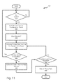
- FIG. 15 illustrates an example order detection process that may be implemented by a character that has assumed the role of master.
- FIG. 16 illustrates an example order detection process that may be implemented by a character that has assumed the role of slave.
- references in the specification to “one embodiment”, “an embodiment”, “an example embodiment”, etc., indicate that the embodiment described may include a particular feature, structure, or characteristic, but every embodiment may not necessarily include the particular feature, structure, or characteristic. Moreover, such phrases are not necessarily referring to the same embodiment. Further, a particular feature, structure, or characteristic described in connection with an embodiment generally may be incorporated into or otherwise implemented by other embodiments regardless of whether explicitly described.
- FIGS. 1A-1C embodiments of an expandable play set 100 are shown.
- FIG. 1A depicts a character 150 coupled to a base unit 110 that is shaped to resemble a rocking-horse.
- FIG. 1B depicts the character 150 of FIG. 1A decoupled from a male connector 112 of the rocking-horse base unit 110 .
- FIG. 1C depicts a high level representation of another base unit 110 of the expandable play set 100 that includes two male connectors 112 that are configured to receive characters 150 such as the character 150 of FIGS. 1A and 1C .
- the expandable play set 100 may include one or more base units 110 and one or more characters 150 .
- a base unit 110 may take the form of a vehicle (e.g., car, plane, scooter, bus, rocking-horse, amusement park ride), a setting (e.g. farm yard, country side, zoo, etc.), a building (e.g., a residence, school, fire station, police station, farm house, etc.) or some other locale with which a child may want to interact.
- a base unit 110 may include one or more male connectors or connection points 112 to which characters 150 may be mechanically and electrically detachably engaged or coupled. Further details concerning male connectors 112 are presented below.
- a base unit 110 may also include one or more loads such as a light emitting diodes, motors, and/or other interactive devices that are electrically connected to the male connectors 112 via one or more wires not shown in FIGS. 1A-1C .
- loads such as a light emitting diodes, motors, and/or other interactive devices that are electrically connected to the male connectors 112 via one or more wires not shown in FIGS. 1A-1C .
- a character 150 may also take a variety of forms.
- a character 150 may include an outer casing or housing 152 in the shape of a figurine or statuette that resembles a person (e.g., a boy, a girl, a zookeeper, a policeman, a fireman, a bus driver), an animal (e.g., a dog, cat, bear, cow, etc.), a robot, or some other personality, creature, etc.
- a depiction of a housing 152 in the shape of a boy is presented in FIG. 2 .
- the outer casing 152 may further provide a female connector 154 that is configured to mechanically engage a cylindrical post 114 of a male connector 112 .
- the female connector 154 may further align terminals or pins 156 of the female connector 154 with annular contacts 116 of the male connector 112 . See, FIG. 3 for a depiction of the pins 156 .
- the character 150 may include a processor 160 , memory 162 , and one or more input/output (I/O) ports or interfaces 166 .
- the processor 160 , memory 162 , and I/O ports 166 may be implemented using discrete components. However, in some embodiments, a single chip microcontroller may implement the processor 160 , memory 162 , I/O ports 166 or portions thereof.
- one or more of the I/O ports 166 may include or be associated with analog-to-digital converter (ADC) circuitry 167 that converts received analog signals to digital values suitable for processing by the processor 160 .
- ADC analog-to-digital converter
- DAC digital-to-analog converter
- the ADC and/or DAC circuitry 167 , 168 may be incorporated into I/O ports 166 of a microcontroller.
- the ADC and/or DAC circuitry 167 , 168 may be provided by external components coupled to I/O ports 166 of a microcontroller.
- the memory 162 may include both volatile memory 163 and non-volatile memory 164 .
- the non-volatile memory 164 may store instructions of a control program to be executed by the processor 160 . Via execution of the instructions, the processor 160 may control operation of the character 150 and the base unit 110 . As explained in greater detail below, the processor 160 , as a result of executing instructions, may identify a male connector 112 to which the character 150 is coupled, identify other characters 150 that are coupled to other male connectors 112 of a base unit 110 , control components of the base unit 110 , control components of the character 150 , and/or exchange data with other characters 150 via the base unit 110 .
- the non-volatile memory 164 may further include data used by the processor 160 such as audio clips to be played back by the processor 160 through an audio speaker 174 .
- the non-volatile memory 164 may store one or more responses for each corresponding ID of a male connector 112 .
- the memory 162 may be provided by a microcontroller in some embodiments. In other embodiments, the memory 162 may be provided or partially provided by one or more components that are external to a microcontroller.
- the character 150 may include a serial peripheral interface (SPI) NOR flash device to store one or more responses (e.g., audio clips, voice data, etc.) to be played back by the processor 160 .
- SPI serial peripheral interface
- FIG. 8 Details for obtaining the ID of a male connector 112 are present in detail below in regard to FIG. 8 .
- Different characters 150 may have different responses for the same ID.
- each character 150 may have more than a single response for the same ID.
- coupling a first character 150 to a male connector 112 of based unit 110 may generate a first set of responses from the first character 150 where coupling a second character 150 to the same male connector 112 may generate a second set of responses that differ from the first set of responses.
- a play set 100 may be designed with approximately 147 different male connector IDs and each character 150 may be programmed with over 400 responses.
- the base units 110 and characters 150 of the play set 100 may be sold separately and/or packages (e.g., a base unit 110 and a character 150 ).
- base units 110 and characters 150 of different packages may be mixed and matched.
- a character 150 sold in a first package may be used with a character 150 and base unit 110 sold in a second package in order to provide new responses and interactions to the character 150 and base unit 110 of the second package.
- additional characters 150 and base units 110 may be added to characters 150 and base units 110 that a child already owns in order to expand upon the play experience.
- the character 150 may further include an electro-mechanical button 170 and associated LED 172 that are coupled to the processor 160 via separate I/O ports 166 . Via such I/O ports 166 , the electro-mechanical button 170 may provide the processor 160 with a signal indicative of whether the button 170 has been pressed and the processor 160 may turn off and turn on the LED 172 as appropriate.
- the character 150 may further include an audio speaker 174 and interface circuitry 176 .
- the audio speaker 174 may be coupled to the processor 160 via an I/O port 166 to permit the processor 160 to playback audio clips stored in the non-volatile memory 164 through the speaker audio 174 .
- the connector interface circuitry 176 may be coupled to the processor 160 via I/O ports 166 to permit the processor 160 to send and/or receive signals to and/or from the male connector 112 .
- the character 150 may include a battery compartment 180 configured to receive one or more batteries 182 and align electrical terminals 184 of such batteries 182 with electrical contacts 186 of the battery compartment 180 . As such, batteries 182 may be placed in the battery compartment 180 in order to deliver electric power to the processor 160 and other electrical components of the character 150 via electrical contacts 186 .
- FIG. 5A-5C three embodiments of the male connectors 112 are shown.
- FIG. 5A depicts a four contact male connector 112 a in which four annular contacts 116 a , 116 b , 116 c , 116 d are positioned about a cylindrical post 114 a .
- FIG. 5B depicts a three contact male connector 112 b in which three annular contacts 116 a , 116 b , 116 c are positioned about a cylindrical post 114 b .
- FIG. 5C depicts a two contact male connector 112 c in which two annular contacts 116 a , 116 b are positioned about a cylindrical post 114 c.
- the character 150 includes a cylindrical female connector 154 configured to mechanically engage the cylindrical post 114 of a male connector 112 and electrically couple pins 156 to the annular contacts 116 .
- the cylindrical female connector 154 permits use of the character 150 with male connectors 112 having different numbers of contacts 116 such as the four, three, and two contact embodiments of FIGS. 5A-5C .
- both the cylindrical female connector 154 of the character 150 and the cylindrical posts 114 of the base units 110 have a circular cross section.
- the circular cross sections permit the characters 150 to be mechanically coupled to the male connectors 112 in a radially-independent manner.
- the male connector 112 corresponds to a driver's seat of a vehicle
- the character 150 may be mechanically coupled to the male connector 112 with the character 150 facing forward, facing backward, facing to the left, facing to the right, or in any radially-facing direction in between.
- each pin 156 a , 156 b , 156 c , 156 d has a longitudinal offset 158 a , 158 b , 158 c , 158 d from a base 153 of the character 150 .
- each annular contact 116 a , 116 b , 116 c , 116 d has a corresponding longitudinal offset 117 a , 117 b , 117 c , 117 d from a base 113 of the male connector 112 .
- the longitudinal offsets 158 a , 158 b , 158 c , 158 d and corresponding longitudinal offsets 117 a , 117 b , 117 c , 117 d are defined such that pins 156 a , 156 b , 156 c , 156 d contact corresponding annular contacts 116 a , 116 b , 116 c , 116 d when the character 150 is fully seated on a male connector 112 a.
- the Y+ annular contact 116 a of each male connector 112 a , 112 b , and 112 c has a longitudinal offset 117 a that roughly corresponds to the longitudinal offset 158 a of a Y+ pin 156 a of the female connector 154 .
- the female connector 154 and corresponding post 114 a , 114 b , 114 c guides the Y+ pin 156 a into contact with the Y+ annular contact 116 a of the respective male connector 112 a , 112 b , 112 c .
- the pins 156 b , 156 c , 156 d and annular contacts 116 b , 116 c , and 116 d operate in a similar manner; however, when the character 150 is coupled to a three contact male connector 112 b , the Motor pin 156 d remains unconnected as male connector 112 b does not include a corresponding Motor annular contact 116 d . Similarly, when the character 150 is coupled to a two contact male connector 112 c , both the GND pin 156 c and the Motor pin 156 d remain unconnected as the male connector 112 c does not contain a corresponding GND annular contact 116 c and a corresponding Motor annular contact 116 d.
- each character 150 in the play set 100 has a fixed number of pins 156 (e.g., four) and the base units 110 may include male connectors 112 with two, three, and/or four contacts 116 .
- the characters 150 in other embodiments may include a different number of pins 156 .
- the play set 100 may include characters 150 with a range of pins 156 (e.g., characters 150 with two connectors as well as characters 150 with four connectors).
- the male connectors 112 in some embodiments may all have a fixed number (e.g., four) of annular contacts 116 .
- the play set 100 may reverse the position of the pins 156 and contacts 116 to where the characters 150 include annular contacts 116 and the male connectors 112 include the pins 156 .
- the male connectors 112 and female connectors 154 may each have a circular cross-section which permits coupling the characters 150 to the male connectors 112 in a radially independent manner.
- Other embodiments may forgo some radial independence by using male connectors 112 and female connectors 154 with different shaped cross-sections.
- both the male connector 112 and the female connector 154 may have an octagonal cross-section that permits the character 150 to have eight different radial facings. See, e.g., FIG. 6A . Radial independence, however, may be achieved or retained with cross-sections other than circular. For example, as shown in FIG.
- radial independence may be achieved via a female connector 154 having a square cross-section and a post 114 of a male connector having a circular cross-section. Conversely, radial independence may also be achieved using a round female connector 154 and a square post 114 as shown in FIG. 6C .
- a pin 156 may be placed on each side of the square female connector 154 to engage an appropriate annular contact 116 of the post 114 .
- the female connector 154 may include annular contacts that engage pins on each side of the post 114 .
- FIG. 7 depicts details regarding aspects of an electrical interface between the female connector 154 and four contact male connectors 112 a .
- Y+, AUX, GND, and Motor pins 156 and corresponding contacts 116 may electrically couple interface circuitry 176 of a character 150 to connector interface circuitry 119 a of a male connector 112 a .
- the processor 160 of a character 150 may identify a male connector 112 a , control one or more aspects of a base unit 110 , and communicate with other characters 150 via connector interface circuitry 119 a , 176 .
- the interface circuitry 176 includes terminals IOA 1 , IOA 4 , IOA 5 , IOA 6 , IOA 7 , IOB 0 , IOB 1 , IOB 2 , IOB 3 , X ⁇ , and X+.
- Each such terminal may be coupled to processor 160 via a corresponding I/O port 166 .
- the processor 160 may read a voltage from and/or apply a voltage to such terminals via the respective I/O ports 166 .
- the IOA 1 terminal is coupled to the drain of transistor Q 7 via resistor R 22 .
- the Motor pin 156 d is coupled to the collector of transistor Q 3 , the drain of transistor Q 6 , and the gate of transistor Q 7 .
- the IOB 2 terminal is also coupled to the drain of the Q 6 transistor and the gate of transistor Q 7 via the diode D 2 and the resistor R 23 .
- the IOA 4 terminal is coupled to the gate of transistor Q 6 , and the source of transistor Q 6 is coupled to ground.
- the IOA 6 terminal is coupled to the base of transistor Q 3 via resistor R 11 and the emitter of transistor Q 3 is coupled to power source VDD.
- the X ⁇ terminal is coupled to the AUX pin 156 b .
- the X+ terminal is coupled to the Y+ pin 156 a via resistor R 3 .
- the IOB 0 terminal is coupled to the Y+ pin 156 a
- the IOB 3 terminal is coupled to the AUX pin 156 b via resistor R 42 .
- the AUX pin 156 b is further coupled to power source VDD via pull-up resistor R 6 .
- the IOB 1 terminal is coupled to the base of transistor Q 2 via resistor R 15 .
- IOA 7 is coupled to the base of transistor Q 5 via resistor R 2 .
- the emitter of transistor Q 2 and the emitter of transistor Q 5 are coupled to power source VDD.
- the collector of transistor Q 2 is coupled to the AUX pin 156 b
- the collector of transistor Q 5 is coupled to the AUX pin 156 b via resistor R 17 .
- the Y+ contact 116 a is coupled to resistor R 31 , which is coupled to light-emitting diode LED 1 , resistor R 30 , and AUX connector 116 b .
- Resistor R 30 is further coupled to ground via a first path through key K 2 and a second path via resistor R 33 .
- light-emitting diode LED 1 is further coupled to ground via a first path that includes resistors R 29 and R 33 and a second path that includes resistor R 29 and key K 2 .
- the Motor contact 116 d is coupled to the GND contact 116 c via light-emitting diode LED 2 and resistor R 47 .
- the Motor contact 116 d is further coupled to the drain of transistor Q 12 via a load such as motor MOTOR.
- the Motor contact 116 d is also coupled to a data line of the communication interface 120 .
- the gate of transistor Q 12 is also coupled to the data line via a resistor R 43 and to GND contact 116 c via capacitor C 26 .
- the data line is further coupled to the GND contact 116 c via a first path that includes pull-down resistor R 28 and a second path that includes key K 1 and resistor R 20 .
- the two contact male connector 112 c does not include GND and Motor contacts 116 c , 116 d .
- the connector interface circuitry 119 c of the two contact male connector 112 c may include only a subset of the components found in the connector interface circuitry 119 a which may reduce implementation costs.
- connector interface circuitry 119 c may merely include resistor R 31 coupled between the Y+ and AUX contacts 116 a , 116 b as indicated by the dotted-line box labeled 119 c in FIG. 7 .
- the three contact male connector 112 b does not include a Motor contact 116 d .
- the connector interface circuitry 119 b of the three contact male connector 112 b may include only a subset of the components found in the connector interface circuitry 119 a which may reduce implementation costs.
- the connector interface circuitry 119 b may include resistor R 31 as well as resisters R 29 , R 30 , R 33 , light-emitting diode LED 1 , and key K 2 as indicated by the dotted-line box labeled 119 b in FIG. 7 .
- the male connectors 112 identify themselves based on resistors R 28 , R 30 , R 31 which in essence provide the male connectors 112 with identification circuitry.
- the combination of resistance values for resistors R 28 , R 30 , R 31 may be varied among male connectors 112 in order to unique identify male connectors 112 .
- the processor 160 may apply voltages to contacts 116 of the male connectors 112 in order to generate voltage levels that are dependent upon the resistors R 28 , R 30 , R 31 and thereby identify a male connector 112 based on the generated voltages.
- the processor 160 at 210 may set the IOB 2 terminal and the IOA 1 terminal to the predetermined high voltage V HIGH .
- a voltage V 1 is developed at terminal IOA 5 that is dependent upon a resistance of resistor R 28 .
- resistor R 28 has a resistance of 100 K ⁇
- a voltage is developed at the gate of transistor Q 7 sufficient to turn on and connect the terminal IOA 5 to ground.
- resistor R 22 if resistance of the resistor R 28 is 0 ⁇ , the transistor Q 7 remains off and the terminal IOA 5 is pulled to the high voltage V HIGH by resistor R 22 .
- the terminal IOA 5 provides the processor 160 with a logic high or “1” value when resistor R 28 is 0 ⁇ or otherwise sufficiently low to prevent turning on the transistor Q 7 or a logic low or “0” value when the resistor R 28 is 100 K ⁇ or sufficiently high to turn on the transistor Q 7 . If the resistor R 28 is not present (e.g., two or three contact male connectors 112 b , 112 c ), resistor R 28 effectively is a very large resistance. As such, setting the IOB 2 and IOA 1 terminals to the high voltage V HIGH will turn on transistor Q 7 and provide a logic low value to the IOA 5 terminal.
- the processor 160 may read the voltage V 1 developed at the IOA 5 terminal to obtain a value indicative of the resistance of resistor R 28 .
- the processor 160 at 230 may set the X+ terminal to a predetermined high voltage V HIGH (e.g. VDD) and the X ⁇ terminal to predetermined low voltage V LOW (e.g., 0V).
- V HIGH e.g. VDD
- V LOW predetermined low voltage
- the processor 160 may read the voltage V 2 developed at the Y+ terminal to obtain a value indicative of the resistance of resistor R 31 .
- the processor 160 at 250 may set IOA 7 to a predetermined low voltage V LOW to turn on transistor Q 5 .
- a voltage V 3 is developed at the AUX pin 156 b that is dependent upon the resistance of resistor R 30 if present.
- the processor 160 may read the voltage V 3 developed at the X ⁇ terminal to obtain a value indicative of the resistance of resistor R 30 . Even if the resistor R 30 is not present (e.g., a two contact male connector 112 c ), the developed voltage V 3 is still indicative of the absence of resistor R 30 . In other words, the processor 160 may detect the absence of the resistor R 30 based on the voltages V 2 and V 3 .
- the processor 160 at 270 may obtain an identifier (ID) for the male connector 112 based upon the obtained values V 1 , V 2 , V 3 .
- ID identifier
- interface circuitry 176 and connector interface circuitry 119 a , 119 b , 119 c essentially generate a binary value for value V 1 , but generate analog values V 2 , V 3 that are subsequently digitized by corresponding IO ports 166 .
- values V 2 and V 3 are likely to vary a bit between readings and between different male connectors 112 that are supposed to have the same ID.
- the processor 160 may obtain an ID for a male connector 112 based upon associated ranges for values V 2 and V 3 .
- the processor 160 may obtain an ID for a male connector 112 that is associated with a four contact male connector 112 a on a base unit 110 known to be shaped as an airplane if value V 1 is a logical high value, value V 2 is between values digital values X and Y and value V 3 is between digital values A and B.
- the processor 160 may use the obtained ID to retrieve an appropriate response from its memory 162 and may execute the retrieved response.
- the processor 160 may cause the character 150 to playback an audio clip that says “I enjoy flying my plane,” or may cause detected base unit 110 to generate an appropriate response such as turn on a motor that slowly rotates a propeller of the plane.
- the processor 160 may obtain an ID of a male connector 112 . As such, the processor 160 may ascertain whether the male connector 112 to which its character 150 is attached is a four, three, or two contact male connector 112 a , 112 b , 112 c . As noted above, the two contact male connector 112 c may merely provide a resistor R 31 for identification purposes. As such, the processor 160 with respect to two contact male connectors 112 c merely identifies the point 112 c and generates an appropriate response. However, four and three contact male connectors 112 a , 112 b enable additional functionality.
- the four and three contact male connector 112 a , 112 b may include a key K 2 and a light-emitting diode LED 1 .
- the processor 160 may set the IOA 7 terminal to a low voltage level V LOW .
- transistor Q 5 turns on and pulls the X ⁇ terminal to a high voltage level V HIGH if key K 2 is not pressed.
- resistors R 17 and R 30 form a voltage divider which reduces the voltage developed at the X ⁇ terminal to a value less than the high voltage level V HIGH .
- the processor 160 may sense whether the key K 2 is pressed by monitoring the value of the X ⁇ terminal when the IOA 7 terminal is set to a low voltage level V LOW .
- the processor 160 may turn on transistor Q 2 by setting the IOB 1 terminal to a low voltage level V LOW such as ground. Turning on transistor Q 2 connects the light-emitting diode LED 1 to a high voltage level V HIGH such as VDD which causes the light-emitting diode LED 1 to illuminate. Conversely, the processor 160 may turn off the transistor Q 2 by setting IOB 1 to a high voltage level V HIGH which causes the light-emitting diode LED 1 to turn off. As such, the processor 160 may turn on and off the light-emitting diode LED 1 as appropriate via the IOB 1 terminal.
- the four point male connector 112 a may further include a key K 1 and a light-emitting diode LED 2 .
- the processor 160 may set the IOB 2 terminal to a high voltage level V HIGH .
- transistor Q 7 turns on thus pulling the IOA 5 terminal to ground if the key K 1 is not pressed.
- transistor Q 7 turns off thus pulling the IOA 5 terminal to a high voltage level V HIGH .
- the processor 160 may sense whether the key K 1 is pressed by monitoring the value of the IOA 5 when the IOB 2 terminal is set a high voltage level V HIGH .
- the processor 150 may only detect the status of K 1 when the load MOTOR is not turned on.
- the processor 160 may turn on transistor Q 3 by setting IOA 6 terminal to a low voltage level V LOW such as ground. Turning on transistor Q 3 connects the light-emitting diode LED 2 to a high voltage level V HIGH such as VDD which causes the light-emitting diode LED 2 to illuminate. Conversely, the processor 160 may turn off the transistor Q 3 by setting IOA 6 to a high voltage level V HIGH which causes the light-emitting diode LED 2 to turn off. As such, the processor 160 may turn on and off the light-emitting diode LED 2 as appropriate via the IOA 6 terminal. In one embodiment, the load MOTOR cannot be used when using LED 2 .
- the base unit 110 includes wires that couple the communications interface 120 of each male connector 112 a together.
- the base unit 110 may include a wire or wires that couple the data lines of each communications interface 120 together.
- the base unit 110 may include a wire or wires that couple ground of each communications interface 120 together.
- the processor 160 may therefore utilize the Motor pin 156 d to communicate with other characters 150 using a bi-directional serial communications protocol over a single data line that is shared by the other characters 150 .
- the processor 160 may use the IOA 5 terminal associated with transistor Q 7 as a DATA IN terminal to receive data from other characters 150 .
- the processor 160 may use the terminal IOA 4 associated with transistor Q 6 as a DATA OUT terminal to transmit data to other characters 150 .
- the processor 160 may further control a load such as motor MOTOR via the Motor pin 156 d .
- the processor 160 may turn on the load by turning the transistor Q 3 on via terminal IOA 6 .
- the processor 160 may set the terminal IOA 6 to a low voltage level V LOW to turn on transistor IOA 6 which causes the capacitor C 26 to charge up. After a short while, the capacitor C 26 may be sufficiently charged to turn on the transistor Q 12 and thereby turn on a load such as the motor MOTOR.
- the processor 160 may turn off the transistor Q 3 by applying a high voltage V HIGH via terminal IOA 6 .
- the processor 160 uses a network or communications protocol that is defined in such a manner that prevents unintended turning on of the load.
- the capacitor C 26 turns on the load a short while after the MOTOR contact 116 d has been at a high level V HIGH .
- the networking protocol in one embodiment, is designed to ensure that the Motor contact 116 d does not remain at the high level V HIGH for a time sufficient to turn on the load. More specifically, the capacitance of capacitor C 26 affects the delay period or charging period required to turns on load.
- the capacitance of capacitor C 26 is selected to ensure there is not too much delay before turning on the load while at the same time ensuring that the charging period is sufficient to prevent communications via the Motor pin 156 d from inadvertently turning on the load.
- the capacitance of the capacitor C 26 is selected such that the capacitor C 26 turns on the load when the Motor contact 116 d is held high for roughly 20 to 40 symbol times.
- the network protocol implemented by the processors 160 of the characters 150 use signals in accordance with those depicted in FIG. 10 .
- the master pulls the data line to a low level V LOW .
- V LOW the data line is low for more than a symbol time as shown at 310 (e.g., at least 125% of a symbol time)
- a master exists.
- the data line is high for more than a symbol time as shown at 320 , then a master does not exist.
- the data line may be further used to transmit a data bit or symbol.
- a master device e.g., a character 150
- the master may transition the data line from a high level V HIGH to a low level V LOW to transmit a data “1” as shown at 330 .
- the master may transition the data line from a low level V LOW to a high level V HIGH to transmit a data “0” as shown at 340 .
- the processors 160 may cause such transitions to occur at roughly the center of a symbol time period.
- the data line may be at the high level V HIGH for the first half of the symbol time and may be at the low level V LOW for the second half of the symbol time period.
- the data line may be at the low level V LOW for the first half of the symbol time period and may be at the high level V HIGH for the second half of the symbol time period.
- An example waveform is provided at 350 in which a master is first advertised followed by the transmission of data bits 1 , 1 , 1 , 0 , 0 , 1 .
- FIGS. 11 and 12 a master selection process 400 that may be implemented by the processors 160 to select a master will be described.
- FIG. 11 depicts a flowchart of the master selection process 400 that may be implemented by each processor 160 .
- FIG. 12 depicts example waveforms on the open drain network as a result of two characters 150 (e.g., Device A and Device B) both attempting to become a master.
- the processor 160 uses phrases such as “the processor 160 permitting the data line to go or float high,” “the processor 160 pulling the data line low,” and similar phrases. Such phrases are used as a matter of convenience. More accurately, the processor 160 generates signals for terminal IOA 4 which turn on or turn off transistor Q 6 which in turn cause the transistor to respectively pull the data line low via Motor pin 156 d or permit the pull-up resistor R 23 to pull the data line high via Motor pin 156 d . Such verbosity would obscure the nature of the following disclosure and the above phrases capture the essence of the processor 160 controlling the resulting pulling up and down of the data line. Similarly, the processor 160 may determine the status of the data line based on signals obtained via transistor Q 7 and the IOA 5 terminal. Again, this concept is captured below as the processor 160 reading or determining the state of the data line despite the fact that the processor 160 may obtain such information via other components such as transistor Q 7 , the IOA 5 terminal, and associated I/O port 166 .
- a processor 160 may determine whether no master is present based on the status of the data line. As noted above, a master pulls the data line low and if no master is present the open drain nature of the network results in the data line being pulled high. Thus, if the data line is high for longer than a symbol time, then the processor 160 at 410 may determine that no master is present. However, if the data line is low or has not been high for more than a symbol time, then the processor 160 may return to 410 to further assess whether a master is present. In this manner, the processor 160 may continually monitor the network for the presence of a master and may attempt to become a master if no master is present.
- the network has been high for more than a symbol period and such status has been read by both Devices A and B.
- both Devices A and B may detect at 410 that no master is present and may proceed to 420 in an attempt to become master.
- the processor 160 may pull the data line low for a short period of (e.g., 4 ms). This short period of being pulled low may reduce the number of devices competing to become the master since not all devices on the network may detect the absence of a master at the same time. In particular, later devices may detect the line pulled low during their monitoring at 410 and thus not proceed to 420 .
- the short period of 420 is reflected in FIG. 12 as period T 2 .
- the processor 160 may clear a counter C.
- the processor 160 may randomly select a time slot value between 0 and a maximum number of time slots MAX ⁇ 1 and continue to hold the data line low for the randomly selected number of time slots.
- the protocol may utilize 32 time slots each having a period of 16 ms.
- the processor 160 may randomly select a value between 0 and 31 and hold the data line low for the selected number of time slots.
- the processor 160 may continue to hold the data line low for an additional 5 time slots or 80 ms in such an embodiment.
- This random period of being held low is shown as period T 3 in FIG. 12 .
- FIG. 12 depicts that Device A has selected a larger time slot value than Device B and thus holding the data line low for a longer period T 3 .
- the processor 160 at 450 may determine whether another device is competing for the role of master. To this end, the processor 160 at 450 may stop pulling the data line low for a short period of time and read the status of the data line. If data line is low, that means another device is competing for the role of master. As such, the processor 160 may return to 410 , thus giving up its current attempt to become master. However, if the data line is high, then another device is not competing for the role of master. Accordingly, the processor 160 at 460 increments its counter C and immediately pulls the data line down to further its pursuit of the role of master.
- the short period of time to read the state at 450 is less than 5% of the time slot period in order to reduce the likelihood of other devices mistakenly detecting that no other device is competing for the role of master.
- the Device B at period T 4 detects that the data line is low and therefore another device is trying to become master. As a result, the Device B may return to 410 and cease its current pursuit of becoming the master.
- Device A at period T 4 detects that the data line is high and therefore that no other device is trying to become master. As such, the Device A increments its counter C and pulls the data line low at 460 .
- the processor 160 at 470 determines whether the counter C has reached a predetermined number (e.g., 3). If the counter C has reached the predetermined count, then the processor 160 has successfully detected that no other device is trying to become master a number of times equal to the predetermined count. Accordingly, the processor 160 may proceed to 480 where the processor 160 may assume the role of master. However, if the counter C has not reached the predetermined count, then the processor 160 may return to 440 to select another random time slot value and repeat the process until the processor 160 either (i) ceases its pursuit of becoming master as a result of detecting another device attempting to become master at 450 , or (ii) obtains the predetermined count C and proceeds to 480 to assume the role of master.
- a predetermined number e.g., 3
- the master selection process is accomplished via a few short pulses.
- the total time to complete the master selection process may be much shorter than a predefined training sequence found in other protocols.
- the total time may also be shorter than the time to transmit a packet containing many bits found in other protocols.
- the master selection process of FIG. 12 may enable a quick master resolution thus permitting master and slave devices to quickly respond to changes in the network configuration. More specifically, a child may repeatedly attach, detach, reattach, reorder, etc. the position of characters 150 with respect to male connectors 112 of a base unit 110 . Quick resolution of the network organization (i.e., which characters 150 at any given time are master or slave) is desired so that the characters 150 may quickly provide a suitable interactive response to the child's actions.
- the frame 500 includes a preamble 510 from master, a start bit 520 from master, M data bits 530 from master, a parity bit 540 from master, and N reply bits 550 from slave.
- M and N are 6 and the preamble 410 corresponds to the master pulling the data line low for more than a symbol period. Due to the open drain implementation of the network, if there is no reply from the slave device, the network signal for the reply period 550 would float high and inadvertently turn on the load (e.g., motor MOTOR). To address this, each reply slot of the reply period 550 is implemented as shown in FIG. 14 .
- the master device pulls up the data line for a short period of time (e.g., 0.1% of the time slot) as shown as period T 1 in FIG. 14 .
- the slave device(s) may derive the timing from the falling edge of the period T 1 pulse for synchronization.
- the master device continues to pull down the data line during period T 2 .
- the slave device provides a reply value. In particular, if the reply is a data “0”, the slave pulls the data line low during period T 3 . Conversely, if the reply is a data “1”, then the slave does not pull the data line low during period T 3 .
- the master may read the data line to obtain the reply bit from the slave. As shown, the master during period T 4 may cease pulling down the data line. As such, the data line achieves the reply value provided by the slave. Thus, the master at 50% of the reply slot may then read the data line to obtain the reply bit from the slave.
- FIG. 14 should make it readily apparent that the master pulls the data line low for all but a few brief periods (e.g., periods T 1 and T 4 of the reply slot). As such, the master ensures that the load is not inadvertently turned on.
- the master may perform collision detection during the start bit 520 , M data bits 530 , and parity bit 540 . In particular, the master may ascertain whether it is able to successfully pull the data line high before each falling edge. If master is unable to successfully pull the data line high before each falling edge, then the master detects a data collision. In response to detecting a data collision, the master continues sending the remaining bits of the frame. The master may relinquish the master role and then attempt to regain the master role via the master selection process 400 described above in regard to FIG. 11 .
- Some play scenarios of the play set 100 detect the order in which characters 150 are coupled to the male connectors 112 d and thus added to the network. The characters 150 may then provide interactive responses based on such detected order.
- an order detection process 400 is shown in FIG. 15 .
- the master is not necessarily the first character 150 to be added to the network. Instead, each character 150 having the role of master implements the order detection process 600 shown in FIG. 15 , and each character having the role of slave implement the order detection process 700 shown in FIG. 16 .
- the characters 150 may implement the master selection process 400 and assume the role of master at 480 .
- the processor 160 of such character 150 at 610 of FIG. 15 may initialize a counter K to zero and send a first polling packet at 620 .
- the processor 160 may determine whether a response to the first polling packet has been received. If a response has not been received, the processor 160 may increment the counter K at 640 .
- the processor may determine whether a predetermined number (e.g. 3) of first polling packets have been sent. In particular, if the counter K equals the predetermined number (e.g. 3), then the processor 160 may determine that the predetermined number have been sent.
- the processor 160 at 660 determines that its character 150 is the first device coupled to the network.
- the processor 160 at 670 then proceeds with normal communications. Otherwise, the process 160 returns to 620 to send another first polling packet.
- the processor 160 at 680 determines that its character 150 was not the first character 150 attached to the network. More specifically, the processor 160 at 680 proceeds as if its character 150 was the second character 150 attached to the network. The processor 160 then at 670 proceeds with normal communications.
- the characters 150 may cease pursuit of the role of master and become a slave.
- the processor 160 may execute the order detection process 700 to ascertain the order devices are connected to the network.
- the processor 160 at 710 may determine that its character 150 by default is the second character to attach to the network.
- the processor 160 at 720 receives a first polling packet
- the processor 160 at 730 sends a reply to the first polling packet.
- the processor 160 at 740 determines its character 150 is the first character 150 attached to the network.
- a few examples of play flow are presented in order to aid in further understanding of how the base units 110 , characters 150 , and communications protocol are intended to interact in one embodiment.
- two characters 150 via the base unit 110 and communications protocol may talk to each other, answer simple questions, and sing together.
- Such singing may take different forms such as singing in parts, synchronized singing together, singing alone, etc.
- the characters 110 may active various interactive devices or loads of the base unit 110 such as, for example, light-emitting diodes and motors.
- certain embodiments may be implemented as a plurality of instructions on a non-transitory, computer-readable storage medium such as, for example, flash memory devices, hard disk devices, compact disc media, DVD media, EEPROMs, etc. Such instructions, when executed by processor 160 , may result in the character 150 implementing various previously described methods and processes.
Priority Applications (1)
| Application Number | Priority Date | Filing Date | Title |
|---|---|---|---|
| US16/241,400 US11305205B2 (en) | 2014-08-15 | 2019-01-07 | Electronic toy with radial independent connector and associated communication protocol |
Applications Claiming Priority (1)
| Application Number | Priority Date | Filing Date | Title |
|---|---|---|---|
| PCT/CN2014/084542 WO2016023234A1 (fr) | 2014-08-15 | 2014-08-15 | Jouet électronique ayant un connecteur indépendant radial, et protocole de communication associé |
Related Parent Applications (1)
| Application Number | Title | Priority Date | Filing Date |
|---|---|---|---|
| PCT/CN2014/084542 Continuation WO2016023234A1 (fr) | 2014-08-15 | 2014-08-15 | Jouet électronique ayant un connecteur indépendant radial, et protocole de communication associé |
Related Child Applications (1)
| Application Number | Title | Priority Date | Filing Date |
|---|---|---|---|
| US16/241,400 Continuation US11305205B2 (en) | 2014-08-15 | 2019-01-07 | Electronic toy with radial independent connector and associated communication protocol |
Publications (2)
| Publication Number | Publication Date |
|---|---|
| US20170157522A1 US20170157522A1 (en) | 2017-06-08 |
| US10173142B2 true US10173142B2 (en) | 2019-01-08 |
Family
ID=55303828
Family Applications (2)
| Application Number | Title | Priority Date | Filing Date |
|---|---|---|---|
| US15/432,343 Active 2034-09-12 US10173142B2 (en) | 2014-08-15 | 2017-02-14 | Electronic toy with radial independent connector and associated communication protocol |
| US16/241,400 Active 2035-07-11 US11305205B2 (en) | 2014-08-15 | 2019-01-07 | Electronic toy with radial independent connector and associated communication protocol |
Family Applications After (1)
| Application Number | Title | Priority Date | Filing Date |
|---|---|---|---|
| US16/241,400 Active 2035-07-11 US11305205B2 (en) | 2014-08-15 | 2019-01-07 | Electronic toy with radial independent connector and associated communication protocol |
Country Status (6)
| Country | Link |
|---|---|
| US (2) | US10173142B2 (fr) |
| EP (2) | EP2996784B1 (fr) |
| CN (1) | CN106852127B (fr) |
| CA (1) | CA2957265C (fr) |
| ES (2) | ES2844051T3 (fr) |
| WO (1) | WO2016023234A1 (fr) |
Cited By (1)
| Publication number | Priority date | Publication date | Assignee | Title |
|---|---|---|---|---|
| US11305205B2 (en) * | 2014-08-15 | 2022-04-19 | Vtech Electronics, Ltd. | Electronic toy with radial independent connector and associated communication protocol |
Families Citing this family (5)
| Publication number | Priority date | Publication date | Assignee | Title |
|---|---|---|---|---|
| CN108704317B (zh) * | 2018-06-08 | 2020-11-27 | 温州普睿达机械科技有限公司 | 一种组合式智能瓜果儿童玩具 |
| US20210339159A1 (en) * | 2018-08-17 | 2021-11-04 | Sony Interactive Entertainment Inc. | Toy system, casing, separate toy, separate toy assessment method, and program |
| US10486078B1 (en) * | 2019-01-18 | 2019-11-26 | Disney Enterprises Inc. | Toy with build-time effects |
| KR102287091B1 (ko) * | 2019-10-08 | 2021-08-06 | 현바오로 | 캐릭터로봇 및 이를 이용한 로봇제어시스템 |
| US11207599B2 (en) * | 2020-02-26 | 2021-12-28 | Disney Enterprises, Inc. | Gameplay system with play augmented by merchandise |
Citations (23)
| Publication number | Priority date | Publication date | Assignee | Title |
|---|---|---|---|---|
| US4820233A (en) * | 1986-01-26 | 1989-04-11 | Weiner Avish J | Sound-producing amusement devices |
| GB2275207A (en) | 1993-02-02 | 1994-08-24 | Tyco Investment Corp | Talking playset |
| US5906369A (en) * | 1997-06-25 | 1999-05-25 | Hasbro, Inc. | Electronic matching game apparatus including sound generating means and method of game play using the same |
| GB2338581A (en) | 1998-06-17 | 1999-12-22 | Paul William Hutley | A plaything |
| WO2001012285A1 (fr) | 1999-08-19 | 2001-02-22 | Kidkids, Inc. | Jouets en reseau |
| US6227931B1 (en) * | 1999-07-02 | 2001-05-08 | Judith Ann Shackelford | Electronic interactive play environment for toy characters |
| US6257948B1 (en) * | 1999-07-13 | 2001-07-10 | Hasbro, Inc. | Talking toy with attachable encoded appendages |
| US20020086612A1 (en) * | 2001-01-03 | 2002-07-04 | Chan Albert Wai Tai | Interactive toy teapot |
| US6524159B1 (en) * | 1999-08-23 | 2003-02-25 | Behrouz Kawarizadeh | Intelligent toy |
| US20030045204A1 (en) * | 2001-08-31 | 2003-03-06 | Chan Albert Wai Tai | Interactive toy play set |
| US6719603B2 (en) * | 2001-08-31 | 2004-04-13 | Thinking Technology, Inc. | Interactive toy play set with sensors |
| US20050215170A1 (en) * | 2004-03-24 | 2005-09-29 | Uncle Milton Industries, Inc. | Toy figure with interchangeable brain having associated voice responses |
| US6991509B1 (en) * | 2002-05-07 | 2006-01-31 | Hasbro, Inc. | Activity toy |
| US20060068366A1 (en) | 2004-09-16 | 2006-03-30 | Edmond Chan | System for entertaining a user |
| EP1688165A1 (fr) | 2003-11-14 | 2006-08-09 | Kohei Nishino | Jouet, procede de transmission de donnees, et systeme de transmission de donnees |
| US7392985B1 (en) * | 2002-07-30 | 2008-07-01 | Peter Ar-Fu Lam | Receiver matrix configured to identify multiple external resistors |
| US20080280268A1 (en) | 2007-05-09 | 2008-11-13 | Mattel, Inc. | Toy system for teaching a language |
| US20090264200A1 (en) * | 2003-10-09 | 2009-10-22 | Cdg Electrohex Ltd. | Electronic card game |
| WO2010007336A1 (fr) | 2008-07-18 | 2010-01-21 | Steven Lipman | Jouets interactifs |
| CN102462963A (zh) | 2010-11-05 | 2012-05-23 | 财团法人资讯工业策进会 | 玩偶互动系统及方法 |
| CN103861287A (zh) | 2012-12-12 | 2014-06-18 | 李晓 | 一种玩具的同步方法、同步文件及玩具 |
| US20150258435A1 (en) * | 2014-03-11 | 2015-09-17 | Microsoft Corporation | Modular construction for interacting with software |
| US9457281B1 (en) * | 2001-09-22 | 2016-10-04 | Peter Ar-Fu Lam | Electronics toy play set |
Family Cites Families (10)
| Publication number | Priority date | Publication date | Assignee | Title |
|---|---|---|---|---|
| US6554679B1 (en) * | 1999-01-29 | 2003-04-29 | Playmates Toys, Inc. | Interactive virtual character doll |
| US6682392B2 (en) * | 2001-04-19 | 2004-01-27 | Thinking Technology, Inc. | Physically interactive electronic toys |
| JP3888558B2 (ja) * | 2004-11-18 | 2007-03-07 | 任天堂株式会社 | 無線ネットワークシステムおよび無線通信プログラム |
| US20070093170A1 (en) * | 2005-10-21 | 2007-04-26 | Yu Zheng | Interactive toy system |
| US8545335B2 (en) * | 2007-09-14 | 2013-10-01 | Tool, Inc. | Toy with memory and USB ports |
| US9461812B2 (en) * | 2013-03-04 | 2016-10-04 | Blackberry Limited | Increased bandwidth encoding scheme |
| US9610500B2 (en) | 2013-03-15 | 2017-04-04 | Disney Enterprise, Inc. | Managing virtual content based on information associated with toy objects |
| EP2777786A3 (fr) * | 2013-03-15 | 2014-12-10 | Disney Enterprises, Inc. | Gestion de contenu virtuel en fonction des informations associées à des jouets |
| US9710423B2 (en) * | 2014-04-02 | 2017-07-18 | Qualcomm Incorporated | Methods to send extra information in-band on inter-integrated circuit (I2C) bus |
| EP2996784B1 (fr) * | 2014-08-15 | 2018-04-04 | VTech Electronics, Ltd. | Jouet électronique ayant un connecteur indépendant radial, et protocole de communication associé |
-
2014
- 2014-08-15 EP EP14873115.1A patent/EP2996784B1/fr active Active
- 2014-08-15 ES ES18150640T patent/ES2844051T3/es active Active
- 2014-08-15 ES ES14873115.1T patent/ES2668463T3/es active Active
- 2014-08-15 WO PCT/CN2014/084542 patent/WO2016023234A1/fr active Application Filing
- 2014-08-15 CN CN201480082712.0A patent/CN106852127B/zh active Active
- 2014-08-15 CA CA2957265A patent/CA2957265C/fr active Active
- 2014-08-15 EP EP18150640.3A patent/EP3345668B1/fr active Active
-
2017
- 2017-02-14 US US15/432,343 patent/US10173142B2/en active Active
-
2019
- 2019-01-07 US US16/241,400 patent/US11305205B2/en active Active
Patent Citations (23)
| Publication number | Priority date | Publication date | Assignee | Title |
|---|---|---|---|---|
| US4820233A (en) * | 1986-01-26 | 1989-04-11 | Weiner Avish J | Sound-producing amusement devices |
| GB2275207A (en) | 1993-02-02 | 1994-08-24 | Tyco Investment Corp | Talking playset |
| US5906369A (en) * | 1997-06-25 | 1999-05-25 | Hasbro, Inc. | Electronic matching game apparatus including sound generating means and method of game play using the same |
| GB2338581A (en) | 1998-06-17 | 1999-12-22 | Paul William Hutley | A plaything |
| US6227931B1 (en) * | 1999-07-02 | 2001-05-08 | Judith Ann Shackelford | Electronic interactive play environment for toy characters |
| US6257948B1 (en) * | 1999-07-13 | 2001-07-10 | Hasbro, Inc. | Talking toy with attachable encoded appendages |
| WO2001012285A1 (fr) | 1999-08-19 | 2001-02-22 | Kidkids, Inc. | Jouets en reseau |
| US6524159B1 (en) * | 1999-08-23 | 2003-02-25 | Behrouz Kawarizadeh | Intelligent toy |
| US20020086612A1 (en) * | 2001-01-03 | 2002-07-04 | Chan Albert Wai Tai | Interactive toy teapot |
| US6719603B2 (en) * | 2001-08-31 | 2004-04-13 | Thinking Technology, Inc. | Interactive toy play set with sensors |
| US20030045204A1 (en) * | 2001-08-31 | 2003-03-06 | Chan Albert Wai Tai | Interactive toy play set |
| US9457281B1 (en) * | 2001-09-22 | 2016-10-04 | Peter Ar-Fu Lam | Electronics toy play set |
| US6991509B1 (en) * | 2002-05-07 | 2006-01-31 | Hasbro, Inc. | Activity toy |
| US7392985B1 (en) * | 2002-07-30 | 2008-07-01 | Peter Ar-Fu Lam | Receiver matrix configured to identify multiple external resistors |
| US20090264200A1 (en) * | 2003-10-09 | 2009-10-22 | Cdg Electrohex Ltd. | Electronic card game |
| EP1688165A1 (fr) | 2003-11-14 | 2006-08-09 | Kohei Nishino | Jouet, procede de transmission de donnees, et systeme de transmission de donnees |
| US20050215170A1 (en) * | 2004-03-24 | 2005-09-29 | Uncle Milton Industries, Inc. | Toy figure with interchangeable brain having associated voice responses |
| US20060068366A1 (en) | 2004-09-16 | 2006-03-30 | Edmond Chan | System for entertaining a user |
| US20080280268A1 (en) | 2007-05-09 | 2008-11-13 | Mattel, Inc. | Toy system for teaching a language |
| WO2010007336A1 (fr) | 2008-07-18 | 2010-01-21 | Steven Lipman | Jouets interactifs |
| CN102462963A (zh) | 2010-11-05 | 2012-05-23 | 财团法人资讯工业策进会 | 玩偶互动系统及方法 |
| CN103861287A (zh) | 2012-12-12 | 2014-06-18 | 李晓 | 一种玩具的同步方法、同步文件及玩具 |
| US20150258435A1 (en) * | 2014-03-11 | 2015-09-17 | Microsoft Corporation | Modular construction for interacting with software |
Non-Patent Citations (6)
| Title |
|---|
| Extended European Search Report for EP14873115, dated Mar. 11, 2016, 8 pages. |
| International Search Report for PCT/CN2014/084542, dated Mar. 30, 2015, 5 pages. |
| Wikipedia Article "1-Wire", 5 pages, https://en.wikipedia.org/w/index.php?oldid=616427329. |
| Wikipedia Article "CAN bus", 12 pages, https://en.wikipedia.org/w/index.php?oldid=617195685. |
| Wikipedia Article "I2C", 14 pages, https://en.wikipedia.org/w/index.php?oldid=616317803. |
| Wikipedia Article "Manchester code", 3 pages, https://en.wikipedia.org/w/index.php?oldid=617047888. |
Cited By (1)
| Publication number | Priority date | Publication date | Assignee | Title |
|---|---|---|---|---|
| US11305205B2 (en) * | 2014-08-15 | 2022-04-19 | Vtech Electronics, Ltd. | Electronic toy with radial independent connector and associated communication protocol |
Also Published As
| Publication number | Publication date |
|---|---|
| US11305205B2 (en) | 2022-04-19 |
| CN106852127A (zh) | 2017-06-13 |
| EP3345668A1 (fr) | 2018-07-11 |
| EP2996784A4 (fr) | 2016-04-13 |
| US20170157522A1 (en) | 2017-06-08 |
| CA2957265C (fr) | 2022-05-17 |
| EP2996784B1 (fr) | 2018-04-04 |
| US20190134518A1 (en) | 2019-05-09 |
| CN106852127B (zh) | 2019-10-18 |
| ES2668463T3 (es) | 2018-05-18 |
| EP3345668B1 (fr) | 2020-12-30 |
| CA2957265A1 (fr) | 2016-02-18 |
| WO2016023234A1 (fr) | 2016-02-18 |
| ES2844051T3 (es) | 2021-07-21 |
| EP2996784A1 (fr) | 2016-03-23 |
Similar Documents
| Publication | Publication Date | Title |
|---|---|---|
| US11305205B2 (en) | Electronic toy with radial independent connector and associated communication protocol | |
| JP5554562B2 (ja) | 玩具積み木システム | |
| US20100041304A1 (en) | Interactive toy system | |
| JP2011500116A (ja) | 玩具構築システム | |
| JP5600177B2 (ja) | 対話式の玩具 | |
| US9108115B1 (en) | Toy responsive to blowing or sound | |
| US20120210897A1 (en) | Plug-n-light musical firework apparatus | |
| GB2511479A (en) | Interacting toys | |
| US6524159B1 (en) | Intelligent toy | |
| WO2020125385A1 (fr) | Bloc de construction de programmation | |
| CN103392303A (zh) | 接收端检测方法、检测电路、光模块及系统 | |
| Watkiss | Learn Electronics with Raspberry Pi | |
| US20200206645A1 (en) | Portable children interactive system | |
| KR102055502B1 (ko) | 모듈러 로봇 시스템 | |
| US7434701B1 (en) | Device for coupling to other devices and unique identification thereof | |
| CN107715470B (zh) | 一种遥控玩具的控制方法、装置及系统 | |
| CN210114825U (zh) | 一种有声光提示的幼儿绕珠玩具 | |
| CN2431937Y (zh) | 电子发声贴纸画面凸板玩具 | |
| CN108211377B (zh) | 一种实现玩具机器人个性化控制的系统 | |
| Clotet Ginovart | Manufacturing of a mobile robot for games and surveillance: Kit-cat | |
| Baharudin et al. | A Laser Pointer Communicating Toy | |
| CN102114351B (zh) | 一种玩具 | |
| CN2195783Y (zh) | 电子卡片式识字算术学习机 | |
| Part | Name_ Date_ | |
| CN201022989Y (zh) | 红外线互动蛋糕娃娃玩具结构 |
Legal Events
| Date | Code | Title | Description |
|---|---|---|---|
| AS | Assignment |
Owner name: VTECH ELECTRONICS, LTD., HONG KONG Free format text: ASSIGNMENT OF ASSIGNORS INTEREST;ASSIGNORS:CHEN, DONG GOU;CHO, PUI LAM;WONG, WAI SING;SIGNING DATES FROM 20170522 TO 20170529;REEL/FRAME:042562/0522 |
|
| STCF | Information on status: patent grant |
Free format text: PATENTED CASE |
|
| MAFP | Maintenance fee payment |
Free format text: PAYMENT OF MAINTENANCE FEE, 4TH YEAR, LARGE ENTITY (ORIGINAL EVENT CODE: M1551); ENTITY STATUS OF PATENT OWNER: LARGE ENTITY Year of fee payment: 4 |