US10156949B2 - Force-touch sensor with multilayered electrodes - Google Patents
Force-touch sensor with multilayered electrodes Download PDFInfo
- Publication number
- US10156949B2 US10156949B2 US15/416,126 US201715416126A US10156949B2 US 10156949 B2 US10156949 B2 US 10156949B2 US 201715416126 A US201715416126 A US 201715416126A US 10156949 B2 US10156949 B2 US 10156949B2
- Authority
- US
- United States
- Prior art keywords
- force
- sensing
- touch
- electrode
- capacitance
- Prior art date
- Legal status (The legal status is an assumption and is not a legal conclusion. Google has not performed a legal analysis and makes no representation as to the accuracy of the status listed.)
- Active, expires
Links
- 239000000758 substrate Substances 0.000 claims abstract description 42
- 239000010410 layer Substances 0.000 claims description 79
- 239000012790 adhesive layer Substances 0.000 claims description 6
- 239000004020 conductor Substances 0.000 claims description 5
- 239000011521 glass Substances 0.000 claims description 4
- 229920000642 polymer Polymers 0.000 claims description 4
- 239000010409 thin film Substances 0.000 claims description 4
- 230000005284 excitation Effects 0.000 description 7
- 230000035945 sensitivity Effects 0.000 description 6
- 238000010586 diagram Methods 0.000 description 5
- 239000003990 capacitor Substances 0.000 description 4
- 230000000694 effects Effects 0.000 description 4
- 239000012141 concentrate Substances 0.000 description 2
- 235000013870 dimethyl polysiloxane Nutrition 0.000 description 2
- 239000004205 dimethyl polysiloxane Substances 0.000 description 2
- 230000005684 electric field Effects 0.000 description 2
- 239000011229 interlayer Substances 0.000 description 2
- 238000000034 method Methods 0.000 description 2
- 229920000435 poly(dimethylsiloxane) Polymers 0.000 description 2
- OKTJSMMVPCPJKN-UHFFFAOYSA-N Carbon Chemical compound [C] OKTJSMMVPCPJKN-UHFFFAOYSA-N 0.000 description 1
- 229920000049 Carbon (fiber) Polymers 0.000 description 1
- RYGMFSIKBFXOCR-UHFFFAOYSA-N Copper Chemical compound [Cu] RYGMFSIKBFXOCR-UHFFFAOYSA-N 0.000 description 1
- ZOKXTWBITQBERF-UHFFFAOYSA-N Molybdenum Chemical compound [Mo] ZOKXTWBITQBERF-UHFFFAOYSA-N 0.000 description 1
- BQCADISMDOOEFD-UHFFFAOYSA-N Silver Chemical compound [Ag] BQCADISMDOOEFD-UHFFFAOYSA-N 0.000 description 1
- ATJFFYVFTNAWJD-UHFFFAOYSA-N Tin Chemical compound [Sn] ATJFFYVFTNAWJD-UHFFFAOYSA-N 0.000 description 1
- 239000000853 adhesive Substances 0.000 description 1
- 230000001070 adhesive effect Effects 0.000 description 1
- 239000000956 alloy Substances 0.000 description 1
- 229910052782 aluminium Inorganic materials 0.000 description 1
- XAGFODPZIPBFFR-UHFFFAOYSA-N aluminium Chemical compound [Al] XAGFODPZIPBFFR-UHFFFAOYSA-N 0.000 description 1
- 230000003321 amplification Effects 0.000 description 1
- 238000013459 approach Methods 0.000 description 1
- 239000004917 carbon fiber Substances 0.000 description 1
- 229910052802 copper Inorganic materials 0.000 description 1
- 239000010949 copper Substances 0.000 description 1
- PCHJSUWPFVWCPO-UHFFFAOYSA-N gold Chemical compound [Au] PCHJSUWPFVWCPO-UHFFFAOYSA-N 0.000 description 1
- 229910052737 gold Inorganic materials 0.000 description 1
- 239000010931 gold Substances 0.000 description 1
- 229910002804 graphite Inorganic materials 0.000 description 1
- 239000010439 graphite Substances 0.000 description 1
- 229910052738 indium Inorganic materials 0.000 description 1
- APFVFJFRJDLVQX-UHFFFAOYSA-N indium atom Chemical compound [In] APFVFJFRJDLVQX-UHFFFAOYSA-N 0.000 description 1
- AMGQUBHHOARCQH-UHFFFAOYSA-N indium;oxotin Chemical compound [In].[Sn]=O AMGQUBHHOARCQH-UHFFFAOYSA-N 0.000 description 1
- 238000005259 measurement Methods 0.000 description 1
- 229910052751 metal Inorganic materials 0.000 description 1
- 239000002184 metal Substances 0.000 description 1
- 150000002739 metals Chemical class 0.000 description 1
- VNWKTOKETHGBQD-UHFFFAOYSA-N methane Chemical compound C VNWKTOKETHGBQD-UHFFFAOYSA-N 0.000 description 1
- 229910052750 molybdenum Inorganic materials 0.000 description 1
- 239000011733 molybdenum Substances 0.000 description 1
- 238000003199 nucleic acid amplification method Methods 0.000 description 1
- 230000003287 optical effect Effects 0.000 description 1
- 239000012858 resilient material Substances 0.000 description 1
- 229910052709 silver Inorganic materials 0.000 description 1
- 239000004332 silver Substances 0.000 description 1
- 229910052718 tin Inorganic materials 0.000 description 1
- WFKWXMTUELFFGS-UHFFFAOYSA-N tungsten Chemical compound [W] WFKWXMTUELFFGS-UHFFFAOYSA-N 0.000 description 1
- 229910052721 tungsten Inorganic materials 0.000 description 1
- 239000010937 tungsten Substances 0.000 description 1
- YVTHLONGBIQYBO-UHFFFAOYSA-N zinc indium(3+) oxygen(2-) Chemical compound [O--].[Zn++].[In+3] YVTHLONGBIQYBO-UHFFFAOYSA-N 0.000 description 1
Images


Classifications
-
- G—PHYSICS
- G06—COMPUTING; CALCULATING OR COUNTING
- G06F—ELECTRIC DIGITAL DATA PROCESSING
- G06F3/00—Input arrangements for transferring data to be processed into a form capable of being handled by the computer; Output arrangements for transferring data from processing unit to output unit, e.g. interface arrangements
- G06F3/01—Input arrangements or combined input and output arrangements for interaction between user and computer
- G06F3/03—Arrangements for converting the position or the displacement of a member into a coded form
- G06F3/041—Digitisers, e.g. for touch screens or touch pads, characterised by the transducing means
- G06F3/044—Digitisers, e.g. for touch screens or touch pads, characterised by the transducing means by capacitive means
- G06F3/0445—Digitisers, e.g. for touch screens or touch pads, characterised by the transducing means by capacitive means using two or more layers of sensing electrodes, e.g. using two layers of electrodes separated by a dielectric layer
-
- G—PHYSICS
- G06—COMPUTING; CALCULATING OR COUNTING
- G06F—ELECTRIC DIGITAL DATA PROCESSING
- G06F3/00—Input arrangements for transferring data to be processed into a form capable of being handled by the computer; Output arrangements for transferring data from processing unit to output unit, e.g. interface arrangements
- G06F3/01—Input arrangements or combined input and output arrangements for interaction between user and computer
- G06F3/03—Arrangements for converting the position or the displacement of a member into a coded form
- G06F3/041—Digitisers, e.g. for touch screens or touch pads, characterised by the transducing means
- G06F3/044—Digitisers, e.g. for touch screens or touch pads, characterised by the transducing means by capacitive means
-
- G—PHYSICS
- G01—MEASURING; TESTING
- G01L—MEASURING FORCE, STRESS, TORQUE, WORK, MECHANICAL POWER, MECHANICAL EFFICIENCY, OR FLUID PRESSURE
- G01L1/00—Measuring force or stress, in general
- G01L1/16—Measuring force or stress, in general using properties of piezoelectric devices
-
- G—PHYSICS
- G01—MEASURING; TESTING
- G01L—MEASURING FORCE, STRESS, TORQUE, WORK, MECHANICAL POWER, MECHANICAL EFFICIENCY, OR FLUID PRESSURE
- G01L1/00—Measuring force or stress, in general
- G01L1/14—Measuring force or stress, in general by measuring variations in capacitance or inductance of electrical elements, e.g. by measuring variations of frequency of electrical oscillators
- G01L1/142—Measuring force or stress, in general by measuring variations in capacitance or inductance of electrical elements, e.g. by measuring variations of frequency of electrical oscillators using capacitors
-
- G—PHYSICS
- G06—COMPUTING; CALCULATING OR COUNTING
- G06F—ELECTRIC DIGITAL DATA PROCESSING
- G06F3/00—Input arrangements for transferring data to be processed into a form capable of being handled by the computer; Output arrangements for transferring data from processing unit to output unit, e.g. interface arrangements
- G06F3/01—Input arrangements or combined input and output arrangements for interaction between user and computer
- G06F3/03—Arrangements for converting the position or the displacement of a member into a coded form
- G06F3/041—Digitisers, e.g. for touch screens or touch pads, characterised by the transducing means
- G06F3/0414—Digitisers, e.g. for touch screens or touch pads, characterised by the transducing means using force sensing means to determine a position
-
- G—PHYSICS
- G06—COMPUTING; CALCULATING OR COUNTING
- G06F—ELECTRIC DIGITAL DATA PROCESSING
- G06F2203/00—Indexing scheme relating to G06F3/00 - G06F3/048
- G06F2203/041—Indexing scheme relating to G06F3/041 - G06F3/045
- G06F2203/04105—Pressure sensors for measuring the pressure or force exerted on the touch surface without providing the touch position
-
- G—PHYSICS
- G06—COMPUTING; CALCULATING OR COUNTING
- G06F—ELECTRIC DIGITAL DATA PROCESSING
- G06F2203/00—Indexing scheme relating to G06F3/00 - G06F3/048
- G06F2203/041—Indexing scheme relating to G06F3/041 - G06F3/045
- G06F2203/04106—Multi-sensing digitiser, i.e. digitiser using at least two different sensing technologies simultaneously or alternatively, e.g. for detecting pen and finger, for saving power or for improving position detection
-
- G—PHYSICS
- G06—COMPUTING; CALCULATING OR COUNTING
- G06F—ELECTRIC DIGITAL DATA PROCESSING
- G06F2203/00—Indexing scheme relating to G06F3/00 - G06F3/048
- G06F2203/041—Indexing scheme relating to G06F3/041 - G06F3/045
- G06F2203/04107—Shielding in digitiser, i.e. guard or shielding arrangements, mostly for capacitive touchscreens, e.g. driven shields, driven grounds
Definitions
- the present invention relates to a sensor, especially to a force-touch sensor with multilayered electrodes.
- the touch display panels become popular as the market growing of the compact and lightweight mobile device.
- the pressure touch control technology has rapid development owing to the maturity of touch-control user interface and serious demand for 3D touch operation. Meanwhile, the broad application of robot in industry is gradually extending to office, hospital and family, and resulting in the rapid increase of need for human touch device.
- the conventional pressure touch control panel generally integrates microelectromechanical sensor at edge or corner of the display panel to sense tactile pressure on the display panel, or locates a plurality of force sensors of micro mechanic in artificial skin of robot for touch and force sensing. The cost of the sensor is high and the assembling of the sensor is difficult.
- artificial skin including conductive rubber, conductive sponge, or carbon fiber can detect the force and variation of resistance by measuring variation of current, but the power consuming is high and accuracy is not good, both of this artificial skin and the aforementioned one cannot sense the proximity of object, thus it still needs lots of effort to improve the pressure touch control panel and human tactile-proximity device.
- the present invention provides a force-touch sensor with multilayered electrodes including: an upper substrate, the upper substrate having a first face and a second face opposite to the first face; a first electrode layer arranged on one face of the upper substrate, the first electrode layer having a plurality of first sensing electrode; a second electrode layer arranged opposite to the first electrode layer, and farther away from the upper substrate than the first electrode layer, having a plurality of second sensing electrodes, each second sensing electrode corresponding to each of the first sensing electrodes, and being electrically connected with one corresponding first sensing electrode to form a plurality of touch sensing electrode; a plurality of touch electrode traces, each touch electrode trace being electrically connected with one corresponding touch sensing electrode and electrically isolated with other touch sensing electrodes; a resilient dielectric layer arranged on a side of the second electrode layer, the side being opposite to the upper substrate, and the resilient dielectric layer being compressively deformed under pressure, and being restoring to original shape and volume if pressure is not present; and a third electrode layer
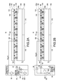
- FIG. 1A shows a schematic view of the force-touch sensor with multilayered electrodes according to an embodiment of the present invention.
- FIG. 1B shows a schematic view of the force-touch sensor with multilayered electrodes according to another embodiment of the present invention.
- FIG. 2A shows a schematic view of the force-touch sensor with multilayered electrodes according to another embodiment of the present invention.
- FIG. 2B shows a schematic view of the force-touch sensor with multilayered electrodes according to another embodiment of the present invention.
- FIG. 3A shows a sectional view of the force-touch sensor with multilayered electrodes according to an embodiment of the present invention.
- FIG. 3B shows a sectional view of the force-touch sensor with multilayered electrodes according to another embodiment of the present invention.
- FIG. 3C shows a sectional view of the force-touch sensor with multilayered electrodes according to another embodiment of the present invention.
- FIG. 4A shows a sectional view of the force-touch sensor with multilayered electrodes according to an embodiment of the present invention.
- FIG. 4B shows a sectional view of the force-touch sensor with multilayered electrodes according to another embodiment of the present invention.
- FIG. 4C shows a sectional view of the force-touch sensor with multilayered electrodes according to another embodiment of the present invention.
- FIG. 5A shows a sectional view of the force-touch sensor with multilayered electrodes according to another embodiment of the present invention.
- FIG. 5B shows a top view of the force-touch sensor with multilayered electrodes according to another embodiment of the present invention.
- FIG. 6 shows a distribution diagram of touch operation signal of the force-touch sensor with multilayered electrodes according to another embodiment of the present invention.
- FIG. 7 shows a distribution diagram of force sensing signal of the force-touch sensor with multilayered electrodes according to another embodiment of the present invention.
- FIG. 8 shows a schematic view of self-capacitance sensing circuit according to an embodiment of the present invention.
- FIG. 1A shows a schematic view of the force-touch sensor with multilayered electrodes according to an embodiment of the present invention.
- a force-touch sensor 10 with multilayered electrode (hereinafter the force-touch sensor 10 ) includes, from top to bottom and the up direction corresponding to the touch point of user finger or touch pen, an upper substrate 100 , a first electrode layer 110 , a second electrode layer 120 , an isolated layer 130 , a resilient dielectric layer 200 , and a third electrode layer 300 .
- the force-touch sensor 10 further includes a plurality of touch electrode traces 150 arranged between the upper substrate 100 and the resilient dielectric layer 200 .
- the upper substrate 100 has a first face 100 a and a second face 100 b opposite to the first face, the first electrode layer 110 is arranged on a face of the upper substrate 100 (for example, the second face 100 b in the embodiment), and the first electrode layer 110 includes a plurality of first sensing electrodes 112 , such as the first sensing electrodes E 11 -E 19 shown in FIG. 1A . It should be noted that this is only a sectional view, the number and distribution of the first sensing electrodes are not limited here.
- the second electrode layer 120 is arranged on a side of the first electrode layer 110 , the side is opposite to the upper substrate 100 , that is, the second electrode layer 120 is farther away from the upper substrate 100 than the first electrode layer 110 .
- the second electrode layer 120 includes a plurality of second sensing electrodes 122 ; each of the second sensing electrodes 122 corresponds to each of the first sensing electrodes 112 , and is electrically connected with the corresponding first sensing electrode 112 to form a plurality of touch sensing electrodes 160 .
- the isolated layer 130 is arranged between the first electrode layer 110 and the second electrode layer 120 .
- the second sensing electrodes 122 are connected with the corresponding first sensing electrodes 112 via the interlayer connection electrodes V 1 -V 9 in the isolated layer 130 .
- the touch electrode traces 150 corresponds to and is connected with a touch sensing electrode 160 , and is isolated with other touch sensing electrodes.
- the touch electrode traces 150 is coplanar with the first sensing electrode 112 and shielded by the second sensing electrodes from projection view (seen from the top view of the force-touch sensor 10 ).
- the first sensing electrode 112 can effectively shield charge interference from finger, and increase the precision of force sensing.
- the resilient dielectric layer 200 is compressively deformed with pressure, and restores to original volume and shape when the pressure is not present.
- the third electrode layer 300 is arranged on a side of the resilient dielectric layer 200 , the side is opposite to the upper substrate 100 , the third electrode layer 300 includes at least one force sensing electrode 170 (for example, the third electrode layer 300 having two force sensing electrodes 170 in FIG. 1A ).
- the corresponding drawings do not show detailed structure of the third electrode layer 300 for simplification, but the third electrode layer 300 includes at least one force sensing electrode 170 .
- the force-touch sensor 10 further includes a capacitance sensing circuit 50 ; the capacitance sensing circuit 50 includes a capacitance excitation driving circuit 52 and a capacitance measuring circuit 54 .
- the capacitance excitation driving circuit 52 includes a signal source 520 and a driving unit 522 , and sends a touch capacitance-excitation signal (stimulus signal) VT to a selected touch sensing electrode 160 (for example, the first sensing electrode E 14 and the second sensing electrode E 24 ) sequentially or randomly.
- a touch capacitance-excitation signal for example, the first sensing electrode E 14 and the second sensing electrode E 24
- the capacitance excitation driving circuit 52 sends the touch capacitance-excitation signal VT to an non-inverting amplifier 56 , a gain of the non-inverting amplifier 56 is preferred to be 1 to generate an auxiliary signal VT 1 with phase same as that of the touch capacitance-excitation signal VT, the auxiliary signal VT 1 is sent to at least one corresponding force sensing electrode 170 . Because the signal with phase same with that of the touch capacitance-excitation signal VT is applied to at least one corresponding force sensing electrode 170 , equivalently, there is only minute (or even no) voltage difference generated between the corresponding selected touch sensing electrode 160 (E 14 ,E 24 ) and at least one corresponding force sensing electrode 170 .
- the auxiliary signal VT 1 can also be sent to all touch sensing electrodes 160 around the selected touch sensing electrodes 160 (E 14 , E 24 ) to eliminate the stray capacitance effect between the selected touch sensing electrode and the surrounding touch sensing electrodes, and concentrate electric field lines on the selected touch sensing electrode, thus increasing the sensitivity of proximity sensing.
- tactile sensing includes touching sensing of user finger actually in contact with the upper substrate 100 , and proximity sensing of user finger close to the upper substrate 100 .
- the tactile sensing includes both touch sensing and proximity sensing.
- the auxiliary signal VT 1 can be used to decrease or eliminate the influence of warp or deformation of the resilient dielectric layer 200 .
- the capacitance measuring circuit 54 of the capacitance sensing circuit 50 can measure the tactile sensing signal Vc 1 at sensing point P, then the touch location can be determined precisely.
- FIG. 1B shows a schematic view of the force-touch sensor with multilayered electrodes according to another embodiment of the present invention, a schematic view of operation of tactile sensing of the force-touch sensor 10 with multilayered electrodes (hereinafter the force-touch sensor 10 ).
- the embodiment in FIG. 1B is similar to that in FIG. 1A , the capacitance excitation driving circuit 52 in the embodiment directly sends the signal source 520 to a non-inverting amplifier 56 (bypassing a driving unit 522 ), a gain of the non-inverting amplifier 56 is preferred to be 1 to generate an auxiliary signal VT 1 with phase same with that of the touch capacitance-excitation signal VT.
- the sensing result is not influenced by the auxiliary signal VT 1 .
- the auxiliary signal VT 1 can be used to decrease or eliminate the influence of warp or deformation of the resilient dielectric layer 200 .
- FIG. 2A shows a schematic view of the force-touch sensor with multilayered electrodes according to another embodiment of the present invention.
- the capacitance excitation driving circuit 52 sends force capacitance-excitation signal Vp to the force sensing electrode 170 of the third electrode layer 300 , and sends a shielding signal Vp 1 with phase same as that of the force capacitance-excitation signal Vp to the non-selected touch sensing electrode 160 (that is, at least part of the first sensing electrodes other than the selected first sensing electrode E 14 , and at least part of the second sensing electrodes other than the corresponding second sensing electrode E 24 ), to shield capacitance variation from finger operation and increase the precision of force sensing.
- the counter-exciting signal Vcount with a predetermined voltage level is sent to the selected touch sensing electrode 160 (E 14 , E 24 ) to enhance the sensitivity of force sensing of the corresponding force sensing electrode 170 .
- the capacitance measuring circuit 54 of the capacitance sensing circuit 50 can measure the force sensing signal Vc 2 from the force sensing electrode 170 at sensing point P, thus determining a touch event being present or not and the value of the force thereof precisely.
- FIG. 2B shows a schematic view of the force-touch sensor with multilayered electrodes according to another embodiment of the present invention, and the force-touch sensor 10 is used for performing force sensing.
- the force-touch sensor 10 is similar to the embodiment shown in FIG. 2A , but the capacitance sensing circuit 50 in FIG. 2B has an inverting amplifier 59 to replace the dc reference signal source 53 .
- the integrated touch and force sensor 10 of the embodiment generates a time varying signal with phase opposite to that of the force capacitance-excitation signal Vp by the inverting amplifier 59 and used as the counter-exciting signal Vcount.
- the sensitivity of force sensing of the second sensing electrode can also be enhanced.
- the non-inverting amplifier 56 in the capacitance sensing circuit 50 is used to generate the shielding signal Vp 1 , an input of the non-inverting amplifier 56 is not connected to an input point of the capacitance measuring circuit 54 .
- the input can be directly connected to the signal source 520 to avoid influence from the force sensing signal Vc 2 at the input point of the capacitance measuring circuit 54 .
- FIG. 3A shows a sectional view of the force-touch sensor with multilayered electrodes according to an embodiment of the present invention.
- the embodiment is similar to that shown in FIG. 1A , but in the embodiment, the touch electrode traces 150 are coplanar with the second sensing electrodes 122 and are electrically connected to the second sensing electrodes 122 one by one correspondingly, and shielded by the first sensing electrodes 112 on the projection respectively.
- the second sensing electrodes 122 are connected to the corresponding first sensing electrodes 112 via the interlayer connection electrodes V 1 -V 9 in the isolated layer 130 , and each of the second sensing electrodes 122 is electrically connected to a corresponding first sensing electrode 112 , thus each touch electrode trace 150 can be electrically connected to the corresponding first sensing electrode 112 .
- the touch electrode traces 150 are shielded by the first sensing electrode 112 on the projection, when the force-touch sensor 10 is performing force sensing, the first sensing electrode 112 can effectively shield the charge interference from finger and make the force sensing more precise. Please refer to FIG. 3B , FIG.
- FIG. 3B shows a sectional view of the force-touch sensor with multilayered electrodes according to another embodiment of the present invention
- the force-touch sensor 10 is similar to that shown in FIG. 3A
- the force-touch sensor 10 in FIG. 3B further includes a second substrate 400
- the second substrate 400 is arranged on a side of the third electrode layer 300
- the side is opposite to the dielectric layer 200 .
- FIG. 3C shows a sectional view of the force-touch sensor with multilayered electrodes according to another embodiment of the present invention
- the force-touch sensor 10 is similar to that shown in FIG. 3B
- the force-touch sensor 10 in FIG. 3C further includes an adhesive layer 500 , the adhesive layer 500 is arranged on a side of the third electrode layer 300 , the side is opposite to the upper substrate 100 .
- FIG. 4A shows a sectional view of the force-touch sensor with multilayered electrodes according to an embodiment of the present invention.
- the embodiment is similar to that shown in FIG. 3A , in the embodiment, the touch electrode traces 150 are arranged between the first sensing electrode 112 and the second sensing electrode 122 .
- each of the touch electrode traces 150 is electrically connected to a corresponding first sensing electrode 112 via the top first layer connection electrodes 132 (V 11 -V 19 ), and is electrically connected to a corresponding second sensing electrode 122 via the bottom second layer connection electrodes 134 (V 21 -V 29 ).
- FIG. 4B shows a sectional view of the force-touch sensor with multilayered electrodes according to another embodiment of the present invention, the force-touch sensor 10 is similar to that shown in FIG. 4A , the force-touch sensor 10 in FIG. 4B further includes a second substrate 400 , the second substrate 400 is arranged on a side of the third electrode layer 300 , the side is opposite to the dielectric layer 200 . Please refer to FIG.
- FIG. 4C shows a sectional view of the force-touch sensor 10 according to another embodiment of the present invention
- the force-touch sensor 10 is similar to that shown in FIG. 4B
- the force-touch sensor 10 in FIG. 4C further includes an adhesive layer 500
- the adhesive layer 500 is arranged on a side of the third electrode layer 300 , the side is opposite to the upper substrate 100 .
- FIG. 5A shows a sectional view of the force-touch sensor 10 according to another embodiment of the present invention, and mainly illustrates an overlapping sectional view of the first sensing electrode 112 , the second sensing electrode 122 , the isolated layer 130 and the touch electrode trace 150 .
- FIG. 5B shows a top view of the force-touch sensor 10 according to another embodiment of the present invention, and mainly illustrates that the first sensing electrodes of the first electrode layer 110 are electrically connected to the second sensing electrode of the second electrode layer 120 one by one correspondingly to form a plurality of the touch sensing electrodes TE 01 - 08 , TE 11 - 18 , TE 21 - 28 , TE 31 - 38 .
- the touch electrode traces 150 are electrically connected to the capacitance sensing circuit 50 and the touch sensing electrodes.
- the force-touch sensor 10 further includes a trace shielding electrode 90 , the trace shielding electrode 90 shields the touch electrode traces 150 to prevent from the degrade of measurement sensitivity, which is caused by the interference on the touch electrode traces 150 .
- FIG. 6 shows a distribution diagram of touch operation signal of the force-touch sensor with multilayered electrodes according to another embodiment of the present invention, and mainly illustrates the distribution of the touch capacitance-excitation signal VT and the auxiliary signal VT 1 when the force-touch sensor 10 is performing touch sensing.
- the first sensing electrodes of the first electrode layer 110 and the second sensing electrodes of the second electrode layer 120 are electrically connected with each other one by one correspondingly to form a plurality of touch sensing electrodes TE 01 - 08 , TE 11 - 18 , TE 21 - 28 , and TE 31 - 38 .
- the capacitance sensing circuit 50 also processes the touch capacitance-excitation signal VT to generate the auxiliary signal VT 1 with phase same as that of the touch capacitance-excitation signal VT, when the force-touch sensor 10 sends a touch capacitance-excitation signal VT to a selected touch sensing electrode TE 14 sequentially or randomly.
- the auxiliary signal VT 1 is sent to at least one corresponding force sensing electrode on the third electrode layer 300 . Because the signal with phase same as that of the touch capacitance-excitation signal VT is sent to at least one corresponding force sensing electrode, equivalently, there is only minute (or even no) voltage difference between the corresponding selected touch sensing electrode TE 14 and at least one corresponding force sensing electrode.
- the minute capacitance will not influence the touch sensing result, thus capacitance interference caused by warped resilient dielectric layer 200 under pressure is prevented, and interference resulting from the parallel capacitance effect between the force sensing electrode and the grounding point is eliminated when sensing the touch operation of the corresponding selected touch sensing electrode TE 14 .
- the auxiliary signal VT 1 can also be sent to all touch sensing electrodes around the selected touch sensing electrode TE 14 to eliminate the stray capacitance effect between the selected touch sensing electrode TE 14 and the surrounding touch sensing electrodes, and concentrate electric field lines on the selected touch sensing electrode, thus increasing the sensitivity of proximity sensing.
- FIG. 7 shows a distribution diagram of force sensing signal of the force-touch sensor 10 according to another embodiment of the present invention, and mainly illustrates the distribution of the force capacitance-excitation signal Vp and the shielding signal Vp 1 when the force-touch sensor 10 is performing force sensing.
- the first sensing electrodes of the first electrode layer 110 and the second sensing electrodes of the second electrode layer 120 are connected with each other one by one correspondingly to form a plurality of touch sensing electrodes TE 01 - 08 , TE 11 - 18 , TE 21 - 28 , and TE 31 - 38 .
- the capacitance sensing circuit 50 processes the force capacitance-excitation signal Vp through non-inverting amplification to generate the shielding signal Vp 1 and sends the shielding signal Vp 1 to non-selected force sensing electrode to shield capacitance variation from finger operation and increase the precision of force sensing, when the capacitance sensing circuit 50 sends the force capacitance-excitation signal Vp for performing force sensing to a corresponding selected force sensing electrode on the third electrode layer 300 . Furthermore, sending a counter-exciting signal Vcount with a predetermined voltage level to the selected touch sensing electrode TE 14 enhances the sensitivity of force sensing of the corresponding force sensing electrode and the precision of determining the force point.
- the first sensing electrodes 112 and the second sensing electrodes 122 may be purposely offset with each other and overlapped with the corresponding electrodes of their adjacent sensing electrodes from projection view. Therefore, the third electrode layer 300 are covered by the touch sensing electrodes TE 01 - 08 , TE 11 - 18 , TE 21 - 28 , TE 31 - 38 , either along the projection view from operation point (upper position) to the third electrode layer 300 (lower position) or along the projection view from the third electrode layer 300 (lower position) to operation point (upper position), thus obtaining an optimal precision when performing force sensing.
- the upper substrate is a polymer thin film or an ultra-thin glass, the upper substrate is not thicker than 500 ⁇ m.
- the upper substrate is a flexible substrate and the upper substrate is not thicker than 500 ⁇ m.
- the lower substrate is a polymer thin film or a glass.
- the resilient dielectric layer 200 is arranged on a side of the second electrode layer, the side is opposite to the upper substrate, the resilient dielectric layer is arranged between the touch sensing electrodes 160 and the force sensing electrodes 170 , and the touch sensing electrodes 160 and the force sensing electrodes 170 are parallel to each other.
- the resilient dielectric layer is compressively deformed with pressure, and restoring to original volume and shape when the pressure is not present.
- the resilient material can be, for example but not limited to, poly dimethyl siloxane (PDMS), optical clear adhesive (OCA).
- the touch capacitance-excitation signal VT and the force capacitance-excitation signal Vp are time varying signals, such as a sinusoidal wave signal, a square wave signal, a triangular wave signal or a trapezoidal wave signal.
- the touch capacitance-excitation signal VT and the force capacitance-excitation signal Vp also can be current sources.
- the counter-exciting signal Vcount is a dc reference signal or a time varying signal with phase opposite to that of the force capacitance-excitation signal Vp.
- the capacitance sensing circuit is, for example, a self-capacitance sensing circuit.
- the touch sensing electrodes 160 and the force sensing electrodes are made of transparent conductive material such as indium tin oxide or indium zinc oxide.
- the touch sensing electrodes 160 and the force sensing electrodes are made of non-transparent conductive material, such as graphite, gold, silver, copper, aluminum, tin, indium, tungsten or molybdenum, or alloy material of any above metals.
- FIG. 8 shows the circuit diagram of the self-capacitance sensing circuit 50 ′ according to an embodiment of the present invention.
- the self-capacitance sensing circuit 50 ′ mainly comprises a capacitance-excitation driving circuit 52 and a capacitance measuring circuit 54 to sense a capacitance change at the sensing point P.
- the capacitance-excitation driving circuit 52 comprises a signal source 520 and a driving unit 522 (including a second impedance 522 a and a third impedance 522 b ).
- the capacitance measuring circuit 54 comprises a differential amplifier 540 , a first impedance 542 and a first capacitor 544 and is used to sense a capacitance change at a sensing electrode 60 , where the sensing electrode 60 comprises a first stray capacitance 62 and a second stray capacitance 64 .
- the signal source 520 is electrically coupled with the first impedance 542 and the second impedance 522 a .
- the first impedance 542 is electrically coupled with the first capacitor 544 and the first capacitor 544 is electrically coupled with the first input end 540 a of the differential amplifier 540 .
- the second impedance 522 a is electrically coupled with the second input end 540 b of the differential amplifier 540 .
- the sensing electrode 60 is electrically coupled to the second impedance 522 a and the second input end 540 b through a node (such as an IC pin) of the self-capacitance sensing circuit 50 ′.
- the first stray capacitance 62 is electrically coupled to the node and the second stray capacitance 64 is electrically coupled to the sensing electrode 60 .
- the sensing electrode 60 receives a touch signal when a finger or a conductor is touched thereon.
- the signal source 520 is a periodical signal and sent to the third impedance 522 , while the resistance values of the first impedance 542 and the second impedance 522 a are identical.
- the differential amplifier 540 will generate a differential touch signal after receiving the signal source 520 and the touch signal from the sensing electrode 60 .
- the capacitance of the first capacitor 544 is equal to the resulting capacitance of the first stray capacitance 62 in parallel connection with the second stray capacitance 64 .
- the capacitance of the second stray capacitance 64 changes when user finger approaches or touches the sensing electrode 60 . Therefore, the voltages fed to the first input end 540 a and the second input end 540 b will be different such that the differential amplifier 540 has a (non-zero) differential output at the output end 540 c . In this way, the minute capacitance change on the sensing electrode 60 can be detected by the differential amplifier 540 . Moreover, the noise from circuits or power source can be advantageously removed.
- the detail of the self-capacitance sensing circuit 50 ′ can be referred to U.S. Pat. No. 8,704,539 (corresponding to Taiwan patent No. 1473001) filed by the same applicant.
Landscapes
- Engineering & Computer Science (AREA)
- General Engineering & Computer Science (AREA)
- Theoretical Computer Science (AREA)
- Physics & Mathematics (AREA)
- General Physics & Mathematics (AREA)
- Human Computer Interaction (AREA)
- Power Engineering (AREA)
- Force Measurement Appropriate To Specific Purposes (AREA)
- Switches That Are Operated By Magnetic Or Electric Fields (AREA)
- Position Input By Displaying (AREA)
- Electronic Switches (AREA)
- Push-Button Switches (AREA)
Applications Claiming Priority (3)
| Application Number | Priority Date | Filing Date | Title |
|---|---|---|---|
| TW105103973A TWI566150B (zh) | 2016-02-05 | 2016-02-05 | 具多層電極結構之高精確度觸壓感應裝置 |
| TW105103973 | 2016-02-05 | ||
| TW105103973A | 2016-02-05 |
Publications (2)
| Publication Number | Publication Date |
|---|---|
| US20170228065A1 US20170228065A1 (en) | 2017-08-10 |
| US10156949B2 true US10156949B2 (en) | 2018-12-18 |
Family
ID=58407955
Family Applications (1)
| Application Number | Title | Priority Date | Filing Date |
|---|---|---|---|
| US15/416,126 Active 2037-05-07 US10156949B2 (en) | 2016-02-05 | 2017-01-26 | Force-touch sensor with multilayered electrodes |
Country Status (3)
| Country | Link |
|---|---|
| US (1) | US10156949B2 (zh) |
| CN (1) | CN107063518B (zh) |
| TW (1) | TWI566150B (zh) |
Cited By (6)
| Publication number | Priority date | Publication date | Assignee | Title |
|---|---|---|---|---|
| US20190361559A1 (en) * | 2017-08-29 | 2019-11-28 | Boe Technology Group Co., Ltd. | Force touch display panel, detection method thereof, and display apparatus |
| US10521014B2 (en) * | 2017-01-19 | 2019-12-31 | Mindmaze Holding Sa | Systems, methods, apparatuses and devices for detecting facial expression and for tracking movement and location in at least one of a virtual and augmented reality system |
| US11195316B2 (en) | 2017-01-19 | 2021-12-07 | Mindmaze Holding Sa | System, method and apparatus for detecting facial expression in a virtual reality system |
| US11328533B1 (en) | 2018-01-09 | 2022-05-10 | Mindmaze Holding Sa | System, method and apparatus for detecting facial expression for motion capture |
| US11495053B2 (en) | 2017-01-19 | 2022-11-08 | Mindmaze Group Sa | Systems, methods, devices and apparatuses for detecting facial expression |
| US11991344B2 (en) | 2017-02-07 | 2024-05-21 | Mindmaze Group Sa | Systems, methods and apparatuses for stereo vision and tracking |
Families Citing this family (9)
| Publication number | Priority date | Publication date | Assignee | Title |
|---|---|---|---|---|
| WO2019035978A2 (en) | 2017-08-15 | 2019-02-21 | Apple Inc. | HYBRID TOUCH SENSOR PANEL ARCHITECTURE WITH CLEAN CAPACITY AND MUTUAL CAPACITY |
| CN107589871B (zh) * | 2017-09-13 | 2020-10-30 | 京东方科技集团股份有限公司 | 一种压感触控模组、制备方法、触摸屏及显示装置 |
| WO2019068020A1 (en) * | 2017-09-29 | 2019-04-04 | Apple Inc. | TOUCH SENSOR PANEL ARCHITECTURE WITH MULTIPLE DETECTION MODE CAPABILITIES |
| CN108534921B (zh) * | 2018-03-26 | 2021-01-26 | 京东方科技集团股份有限公司 | 压力传感器、显示装置 |
| CN109101138A (zh) * | 2018-08-21 | 2018-12-28 | 武汉华星光电半导体显示技术有限公司 | 阵列基板及显示面板 |
| CN110874158A (zh) * | 2018-09-04 | 2020-03-10 | 天马日本株式会社 | 触觉呈现设备 |
| WO2020068330A1 (en) | 2018-09-28 | 2020-04-02 | Apple Inc. | Touch sensor panel |
| CN110231890B (zh) * | 2019-06-28 | 2022-04-29 | 京东方科技集团股份有限公司 | 一种压力感应器件、显示面板及其制作方法、显示设备 |
| CN110307777B (zh) * | 2019-06-28 | 2021-03-05 | 上海天马微电子有限公司 | 一种压感面板及显示装置 |
Citations (16)
| Publication number | Priority date | Publication date | Assignee | Title |
|---|---|---|---|---|
| US5942733A (en) * | 1992-06-08 | 1999-08-24 | Synaptics, Inc. | Stylus input capacitive touchpad sensor |
| US6002389A (en) * | 1996-04-24 | 1999-12-14 | Logitech, Inc. | Touch and pressure sensing method and apparatus |
| US20070257821A1 (en) * | 2006-04-20 | 2007-11-08 | Son Jae S | Reconfigurable tactile sensor input device |
| US20110080373A1 (en) * | 2009-10-07 | 2011-04-07 | Wintek Corporation | Touch Panel and Display Device Using the Same |
| TW201305879A (zh) * | 2011-06-24 | 2013-02-01 | Nissha Printing | 具按壓檢測功能之觸控面板 |
| US8627716B2 (en) * | 2009-02-06 | 2014-01-14 | Pressure Profile Systems Inc. | Capacitive proximity tactile sensor |
| US20140062933A1 (en) * | 2012-08-29 | 2014-03-06 | Sharp Kabushiki Kaisha | Capacitive touch panel with a 'dual layer' force sensor |
| US20140238152A1 (en) * | 2013-02-27 | 2014-08-28 | Synaptics Incorporated | Device and method for localized force sensing |
| US20150130742A1 (en) * | 2013-11-12 | 2015-05-14 | Microsoft Corporation | Multi-Touch Capacitive Sensing Surface |
| CN104897317A (zh) * | 2015-06-18 | 2015-09-09 | 西安电子科技大学 | 基于仿生结构的柔性触-压觉传感器 |
| US20150277626A1 (en) * | 2014-03-28 | 2015-10-01 | Sony Corporation | Sensor device, input device, and electronic apparatus |
| CN205015877U (zh) * | 2015-09-30 | 2016-02-03 | 南昌欧菲光科技有限公司 | 触摸显示装置 |
| US20160077648A1 (en) * | 2014-09-11 | 2016-03-17 | Synaptics Incorporated | Device and method for localized force sensing |
| TWM522414U (zh) * | 2016-02-05 | 2016-05-21 | 速博思股份有限公司 | 具多層電極結構之高精確度觸壓感應裝置 |
| US20170205930A1 (en) * | 2016-01-18 | 2017-07-20 | Superc-Touch Corporation | Capacitive pressure sensor and method for the same |
| US20170269773A1 (en) * | 2016-03-15 | 2017-09-21 | Japan Display Inc. | Display device and display method |
Family Cites Families (4)
| Publication number | Priority date | Publication date | Assignee | Title |
|---|---|---|---|---|
| JP5376446B2 (ja) * | 2009-07-24 | 2013-12-25 | 株式会社ジャパンディスプレイ | 静電容量型入力装置および入力機能付き表示装置 |
| CN102609159A (zh) * | 2011-01-18 | 2012-07-25 | 松翰科技股份有限公司 | 电容式触控装置及其感测装置与多触碰点检测方法 |
| TWI472979B (zh) * | 2012-10-22 | 2015-02-11 | Superc Touch Coporation | 可重組感測點之觸控面板裝置及感測方法 |
| KR101598412B1 (ko) * | 2015-02-11 | 2016-02-29 | 주식회사 하이딥 | 전극 시트 및 터치 입력 장치 |
-
2016
- 2016-02-05 TW TW105103973A patent/TWI566150B/zh active
-
2017
- 2017-01-04 CN CN201710004259.7A patent/CN107063518B/zh active Active
- 2017-01-26 US US15/416,126 patent/US10156949B2/en active Active
Patent Citations (16)
| Publication number | Priority date | Publication date | Assignee | Title |
|---|---|---|---|---|
| US5942733A (en) * | 1992-06-08 | 1999-08-24 | Synaptics, Inc. | Stylus input capacitive touchpad sensor |
| US6002389A (en) * | 1996-04-24 | 1999-12-14 | Logitech, Inc. | Touch and pressure sensing method and apparatus |
| US20070257821A1 (en) * | 2006-04-20 | 2007-11-08 | Son Jae S | Reconfigurable tactile sensor input device |
| US8627716B2 (en) * | 2009-02-06 | 2014-01-14 | Pressure Profile Systems Inc. | Capacitive proximity tactile sensor |
| US20110080373A1 (en) * | 2009-10-07 | 2011-04-07 | Wintek Corporation | Touch Panel and Display Device Using the Same |
| TW201305879A (zh) * | 2011-06-24 | 2013-02-01 | Nissha Printing | 具按壓檢測功能之觸控面板 |
| US20140062933A1 (en) * | 2012-08-29 | 2014-03-06 | Sharp Kabushiki Kaisha | Capacitive touch panel with a 'dual layer' force sensor |
| US20140238152A1 (en) * | 2013-02-27 | 2014-08-28 | Synaptics Incorporated | Device and method for localized force sensing |
| US20150130742A1 (en) * | 2013-11-12 | 2015-05-14 | Microsoft Corporation | Multi-Touch Capacitive Sensing Surface |
| US20150277626A1 (en) * | 2014-03-28 | 2015-10-01 | Sony Corporation | Sensor device, input device, and electronic apparatus |
| US20160077648A1 (en) * | 2014-09-11 | 2016-03-17 | Synaptics Incorporated | Device and method for localized force sensing |
| CN104897317A (zh) * | 2015-06-18 | 2015-09-09 | 西安电子科技大学 | 基于仿生结构的柔性触-压觉传感器 |
| CN205015877U (zh) * | 2015-09-30 | 2016-02-03 | 南昌欧菲光科技有限公司 | 触摸显示装置 |
| US20170205930A1 (en) * | 2016-01-18 | 2017-07-20 | Superc-Touch Corporation | Capacitive pressure sensor and method for the same |
| TWM522414U (zh) * | 2016-02-05 | 2016-05-21 | 速博思股份有限公司 | 具多層電極結構之高精確度觸壓感應裝置 |
| US20170269773A1 (en) * | 2016-03-15 | 2017-09-21 | Japan Display Inc. | Display device and display method |
Non-Patent Citations (1)
| Title |
|---|
| English translation of Taiwan office action dated Sep. 10, 2016. * |
Cited By (9)
| Publication number | Priority date | Publication date | Assignee | Title |
|---|---|---|---|---|
| US10521014B2 (en) * | 2017-01-19 | 2019-12-31 | Mindmaze Holding Sa | Systems, methods, apparatuses and devices for detecting facial expression and for tracking movement and location in at least one of a virtual and augmented reality system |
| US11195316B2 (en) | 2017-01-19 | 2021-12-07 | Mindmaze Holding Sa | System, method and apparatus for detecting facial expression in a virtual reality system |
| US11495053B2 (en) | 2017-01-19 | 2022-11-08 | Mindmaze Group Sa | Systems, methods, devices and apparatuses for detecting facial expression |
| US11709548B2 (en) | 2017-01-19 | 2023-07-25 | Mindmaze Group Sa | Systems, methods, devices and apparatuses for detecting facial expression |
| US11989340B2 (en) | 2017-01-19 | 2024-05-21 | Mindmaze Group Sa | Systems, methods, apparatuses and devices for detecting facial expression and for tracking movement and location in at least one of a virtual and augmented reality system |
| US11991344B2 (en) | 2017-02-07 | 2024-05-21 | Mindmaze Group Sa | Systems, methods and apparatuses for stereo vision and tracking |
| US20190361559A1 (en) * | 2017-08-29 | 2019-11-28 | Boe Technology Group Co., Ltd. | Force touch display panel, detection method thereof, and display apparatus |
| US10976854B2 (en) * | 2017-08-29 | 2021-04-13 | Boe Technology Group Co., Ltd. | Force touch display panel, detection method thereof, and display apparatus |
| US11328533B1 (en) | 2018-01-09 | 2022-05-10 | Mindmaze Holding Sa | System, method and apparatus for detecting facial expression for motion capture |
Also Published As
| Publication number | Publication date |
|---|---|
| CN107063518B (zh) | 2019-11-08 |
| TWI566150B (zh) | 2017-01-11 |
| TW201729050A (zh) | 2017-08-16 |
| CN107063518A (zh) | 2017-08-18 |
| US20170228065A1 (en) | 2017-08-10 |
Similar Documents
| Publication | Publication Date | Title |
|---|---|---|
| US10156949B2 (en) | Force-touch sensor with multilayered electrodes | |
| US9965079B2 (en) | Pressure-sensitive touch screen and touch display screen and electronic device | |
| US8120371B2 (en) | Object position sensing apparatus | |
| US10331267B2 (en) | Touch detection method and touch detector performing the same | |
| US8487901B2 (en) | Display device | |
| US10146984B2 (en) | Mobile device with high-accuracy fingerprint identification | |
| US10209805B2 (en) | Integral sensing apparatus for touch and force sensing and method for the same | |
| CN107402660B (zh) | 具有金属走线的压力触控装置 | |
| US9535545B2 (en) | Common mode noise suppression during hovering and proximity detection | |
| CN107436703B (zh) | 触摸传感器补偿电路 | |
| US10120479B2 (en) | Capacitive pressure sensor and method for the same | |
| KR101739791B1 (ko) | 압력 센싱 장치, 압력 검출기 및 이들을 포함하는 장치 | |
| US10061437B2 (en) | Active canceling of display noise in simultaneous display and touch sensing using an impulse response | |
| US9098155B2 (en) | Self-capacitance measurement using compensation capacitor | |
| JP2015143967A (ja) | タッチセンサ装置及び電子機器並びにタッチジェスチャー検知プログラム | |
| JP2000047808A (ja) | 押圧検出兼用静電容量式座標検出装置 | |
| US10180751B2 (en) | Sensing device for force and tactile-proximity sensing | |
| WO2013128981A1 (ja) | タッチセンサ付携帯型装置及び表示装置 | |
| TWM522414U (zh) | 具多層電極結構之高精確度觸壓感應裝置 | |
| US10055044B2 (en) | Integral sensing apparatus for touch and pressure sensing and method for the same | |
| US10055060B2 (en) | Integral sensing apparatus for touch and force sensing and method for the same | |
| US10289241B2 (en) | Sensing apparatus for touch and force sensing | |
| JP7178972B2 (ja) | タッチパネル及び表示装置 | |
| US20170344169A1 (en) | Integral apparatus for sensing touch and force | |
| KR101645668B1 (ko) | 커패시턴스 측정 회로 및 이를 포함하는 터치 입력 장치 |
Legal Events
| Date | Code | Title | Description |
|---|---|---|---|
| AS | Assignment |
Owner name: SUPERC-TOUCH CORPORATION, TAIWAN Free format text: ASSIGNMENT OF ASSIGNORS INTEREST;ASSIGNORS:LEE, HSIANG-YU;CHIN, SHANG;LIN, PING-TSUN;REEL/FRAME:041091/0404 Effective date: 20161007 |
|
| STCF | Information on status: patent grant |
Free format text: PATENTED CASE |
|
| MAFP | Maintenance fee payment |
Free format text: PAYMENT OF MAINTENANCE FEE, 4TH YR, SMALL ENTITY (ORIGINAL EVENT CODE: M2551); ENTITY STATUS OF PATENT OWNER: SMALL ENTITY Year of fee payment: 4 |