US10147356B2 - OLED pixel driving circuit and OLED display device - Google Patents
OLED pixel driving circuit and OLED display device Download PDFInfo
- Publication number
- US10147356B2 US10147356B2 US15/519,837 US201715519837A US10147356B2 US 10147356 B2 US10147356 B2 US 10147356B2 US 201715519837 A US201715519837 A US 201715519837A US 10147356 B2 US10147356 B2 US 10147356B2
- Authority
- US
- United States
- Prior art keywords
- thin film
- film transistor
- voltage level
- pin
- switch
- Prior art date
- Legal status (The legal status is an assumption and is not a legal conclusion. Google has not performed a legal analysis and makes no representation as to the accuracy of the status listed.)
- Active, expires
Links
Images


Classifications
-
- G—PHYSICS
- G09—EDUCATION; CRYPTOGRAPHY; DISPLAY; ADVERTISING; SEALS
- G09G—ARRANGEMENTS OR CIRCUITS FOR CONTROL OF INDICATING DEVICES USING STATIC MEANS TO PRESENT VARIABLE INFORMATION
- G09G3/00—Control arrangements or circuits, of interest only in connection with visual indicators other than cathode-ray tubes
- G09G3/20—Control arrangements or circuits, of interest only in connection with visual indicators other than cathode-ray tubes for presentation of an assembly of a number of characters, e.g. a page, by composing the assembly by combination of individual elements arranged in a matrix no fixed position being assigned to or needed to be assigned to the individual characters or partial characters
- G09G3/22—Control arrangements or circuits, of interest only in connection with visual indicators other than cathode-ray tubes for presentation of an assembly of a number of characters, e.g. a page, by composing the assembly by combination of individual elements arranged in a matrix no fixed position being assigned to or needed to be assigned to the individual characters or partial characters using controlled light sources
- G09G3/30—Control arrangements or circuits, of interest only in connection with visual indicators other than cathode-ray tubes for presentation of an assembly of a number of characters, e.g. a page, by composing the assembly by combination of individual elements arranged in a matrix no fixed position being assigned to or needed to be assigned to the individual characters or partial characters using controlled light sources using electroluminescent panels
- G09G3/32—Control arrangements or circuits, of interest only in connection with visual indicators other than cathode-ray tubes for presentation of an assembly of a number of characters, e.g. a page, by composing the assembly by combination of individual elements arranged in a matrix no fixed position being assigned to or needed to be assigned to the individual characters or partial characters using controlled light sources using electroluminescent panels semiconductive, e.g. using light-emitting diodes [LED]
- G09G3/3208—Control arrangements or circuits, of interest only in connection with visual indicators other than cathode-ray tubes for presentation of an assembly of a number of characters, e.g. a page, by composing the assembly by combination of individual elements arranged in a matrix no fixed position being assigned to or needed to be assigned to the individual characters or partial characters using controlled light sources using electroluminescent panels semiconductive, e.g. using light-emitting diodes [LED] organic, e.g. using organic light-emitting diodes [OLED]
- G09G3/3225—Control arrangements or circuits, of interest only in connection with visual indicators other than cathode-ray tubes for presentation of an assembly of a number of characters, e.g. a page, by composing the assembly by combination of individual elements arranged in a matrix no fixed position being assigned to or needed to be assigned to the individual characters or partial characters using controlled light sources using electroluminescent panels semiconductive, e.g. using light-emitting diodes [LED] organic, e.g. using organic light-emitting diodes [OLED] using an active matrix
- G09G3/3233—Control arrangements or circuits, of interest only in connection with visual indicators other than cathode-ray tubes for presentation of an assembly of a number of characters, e.g. a page, by composing the assembly by combination of individual elements arranged in a matrix no fixed position being assigned to or needed to be assigned to the individual characters or partial characters using controlled light sources using electroluminescent panels semiconductive, e.g. using light-emitting diodes [LED] organic, e.g. using organic light-emitting diodes [OLED] using an active matrix with pixel circuitry controlling the current through the light-emitting element
-
- G—PHYSICS
- G09—EDUCATION; CRYPTOGRAPHY; DISPLAY; ADVERTISING; SEALS
- G09G—ARRANGEMENTS OR CIRCUITS FOR CONTROL OF INDICATING DEVICES USING STATIC MEANS TO PRESENT VARIABLE INFORMATION
- G09G3/00—Control arrangements or circuits, of interest only in connection with visual indicators other than cathode-ray tubes
- G09G3/20—Control arrangements or circuits, of interest only in connection with visual indicators other than cathode-ray tubes for presentation of an assembly of a number of characters, e.g. a page, by composing the assembly by combination of individual elements arranged in a matrix no fixed position being assigned to or needed to be assigned to the individual characters or partial characters
- G09G3/22—Control arrangements or circuits, of interest only in connection with visual indicators other than cathode-ray tubes for presentation of an assembly of a number of characters, e.g. a page, by composing the assembly by combination of individual elements arranged in a matrix no fixed position being assigned to or needed to be assigned to the individual characters or partial characters using controlled light sources
- G09G3/30—Control arrangements or circuits, of interest only in connection with visual indicators other than cathode-ray tubes for presentation of an assembly of a number of characters, e.g. a page, by composing the assembly by combination of individual elements arranged in a matrix no fixed position being assigned to or needed to be assigned to the individual characters or partial characters using controlled light sources using electroluminescent panels
- G09G3/32—Control arrangements or circuits, of interest only in connection with visual indicators other than cathode-ray tubes for presentation of an assembly of a number of characters, e.g. a page, by composing the assembly by combination of individual elements arranged in a matrix no fixed position being assigned to or needed to be assigned to the individual characters or partial characters using controlled light sources using electroluminescent panels semiconductive, e.g. using light-emitting diodes [LED]
- G09G3/3208—Control arrangements or circuits, of interest only in connection with visual indicators other than cathode-ray tubes for presentation of an assembly of a number of characters, e.g. a page, by composing the assembly by combination of individual elements arranged in a matrix no fixed position being assigned to or needed to be assigned to the individual characters or partial characters using controlled light sources using electroluminescent panels semiconductive, e.g. using light-emitting diodes [LED] organic, e.g. using organic light-emitting diodes [OLED]
- G09G3/3225—Control arrangements or circuits, of interest only in connection with visual indicators other than cathode-ray tubes for presentation of an assembly of a number of characters, e.g. a page, by composing the assembly by combination of individual elements arranged in a matrix no fixed position being assigned to or needed to be assigned to the individual characters or partial characters using controlled light sources using electroluminescent panels semiconductive, e.g. using light-emitting diodes [LED] organic, e.g. using organic light-emitting diodes [OLED] using an active matrix
- G09G3/3258—Control arrangements or circuits, of interest only in connection with visual indicators other than cathode-ray tubes for presentation of an assembly of a number of characters, e.g. a page, by composing the assembly by combination of individual elements arranged in a matrix no fixed position being assigned to or needed to be assigned to the individual characters or partial characters using controlled light sources using electroluminescent panels semiconductive, e.g. using light-emitting diodes [LED] organic, e.g. using organic light-emitting diodes [OLED] using an active matrix with pixel circuitry controlling the voltage across the light-emitting element
-
- G—PHYSICS
- G09—EDUCATION; CRYPTOGRAPHY; DISPLAY; ADVERTISING; SEALS
- G09G—ARRANGEMENTS OR CIRCUITS FOR CONTROL OF INDICATING DEVICES USING STATIC MEANS TO PRESENT VARIABLE INFORMATION
- G09G3/00—Control arrangements or circuits, of interest only in connection with visual indicators other than cathode-ray tubes
- G09G3/20—Control arrangements or circuits, of interest only in connection with visual indicators other than cathode-ray tubes for presentation of an assembly of a number of characters, e.g. a page, by composing the assembly by combination of individual elements arranged in a matrix no fixed position being assigned to or needed to be assigned to the individual characters or partial characters
- G09G3/22—Control arrangements or circuits, of interest only in connection with visual indicators other than cathode-ray tubes for presentation of an assembly of a number of characters, e.g. a page, by composing the assembly by combination of individual elements arranged in a matrix no fixed position being assigned to or needed to be assigned to the individual characters or partial characters using controlled light sources
- G09G3/30—Control arrangements or circuits, of interest only in connection with visual indicators other than cathode-ray tubes for presentation of an assembly of a number of characters, e.g. a page, by composing the assembly by combination of individual elements arranged in a matrix no fixed position being assigned to or needed to be assigned to the individual characters or partial characters using controlled light sources using electroluminescent panels
- G09G3/32—Control arrangements or circuits, of interest only in connection with visual indicators other than cathode-ray tubes for presentation of an assembly of a number of characters, e.g. a page, by composing the assembly by combination of individual elements arranged in a matrix no fixed position being assigned to or needed to be assigned to the individual characters or partial characters using controlled light sources using electroluminescent panels semiconductive, e.g. using light-emitting diodes [LED]
- G09G3/3208—Control arrangements or circuits, of interest only in connection with visual indicators other than cathode-ray tubes for presentation of an assembly of a number of characters, e.g. a page, by composing the assembly by combination of individual elements arranged in a matrix no fixed position being assigned to or needed to be assigned to the individual characters or partial characters using controlled light sources using electroluminescent panels semiconductive, e.g. using light-emitting diodes [LED] organic, e.g. using organic light-emitting diodes [OLED]
- G09G3/3275—Details of drivers for data electrodes
- G09G3/3283—Details of drivers for data electrodes in which the data driver supplies a variable data current for setting the current through, or the voltage across, the light-emitting elements
-
- G—PHYSICS
- G09—EDUCATION; CRYPTOGRAPHY; DISPLAY; ADVERTISING; SEALS
- G09G—ARRANGEMENTS OR CIRCUITS FOR CONTROL OF INDICATING DEVICES USING STATIC MEANS TO PRESENT VARIABLE INFORMATION
- G09G2300/00—Aspects of the constitution of display devices
- G09G2300/04—Structural and physical details of display devices
- G09G2300/0439—Pixel structures
- G09G2300/0465—Improved aperture ratio, e.g. by size reduction of the pixel circuit, e.g. for improving the pixel density or the maximum displayable luminance or brightness
-
- G—PHYSICS
- G09—EDUCATION; CRYPTOGRAPHY; DISPLAY; ADVERTISING; SEALS
- G09G—ARRANGEMENTS OR CIRCUITS FOR CONTROL OF INDICATING DEVICES USING STATIC MEANS TO PRESENT VARIABLE INFORMATION
- G09G2300/00—Aspects of the constitution of display devices
- G09G2300/08—Active matrix structure, i.e. with use of active elements, inclusive of non-linear two terminal elements, in the pixels together with light emitting or modulating elements
- G09G2300/0809—Several active elements per pixel in active matrix panels
- G09G2300/0819—Several active elements per pixel in active matrix panels used for counteracting undesired variations, e.g. feedback or autozeroing
-
- G—PHYSICS
- G09—EDUCATION; CRYPTOGRAPHY; DISPLAY; ADVERTISING; SEALS
- G09G—ARRANGEMENTS OR CIRCUITS FOR CONTROL OF INDICATING DEVICES USING STATIC MEANS TO PRESENT VARIABLE INFORMATION
- G09G2300/00—Aspects of the constitution of display devices
- G09G2300/08—Active matrix structure, i.e. with use of active elements, inclusive of non-linear two terminal elements, in the pixels together with light emitting or modulating elements
- G09G2300/0809—Several active elements per pixel in active matrix panels
- G09G2300/0842—Several active elements per pixel in active matrix panels forming a memory circuit, e.g. a dynamic memory with one capacitor
-
- G—PHYSICS
- G09—EDUCATION; CRYPTOGRAPHY; DISPLAY; ADVERTISING; SEALS
- G09G—ARRANGEMENTS OR CIRCUITS FOR CONTROL OF INDICATING DEVICES USING STATIC MEANS TO PRESENT VARIABLE INFORMATION
- G09G2310/00—Command of the display device
- G09G2310/02—Addressing, scanning or driving the display screen or processing steps related thereto
- G09G2310/0264—Details of driving circuits
- G09G2310/027—Details of drivers for data electrodes, the drivers handling digital grey scale data, e.g. use of D/A converters
-
- G—PHYSICS
- G09—EDUCATION; CRYPTOGRAPHY; DISPLAY; ADVERTISING; SEALS
- G09G—ARRANGEMENTS OR CIRCUITS FOR CONTROL OF INDICATING DEVICES USING STATIC MEANS TO PRESENT VARIABLE INFORMATION
- G09G2310/00—Command of the display device
- G09G2310/08—Details of timing specific for flat panels, other than clock recovery
-
- G—PHYSICS
- G09—EDUCATION; CRYPTOGRAPHY; DISPLAY; ADVERTISING; SEALS
- G09G—ARRANGEMENTS OR CIRCUITS FOR CONTROL OF INDICATING DEVICES USING STATIC MEANS TO PRESENT VARIABLE INFORMATION
- G09G2320/00—Control of display operating conditions
- G09G2320/02—Improving the quality of display appearance
- G09G2320/0233—Improving the luminance or brightness uniformity across the screen
-
- G—PHYSICS
- G09—EDUCATION; CRYPTOGRAPHY; DISPLAY; ADVERTISING; SEALS
- G09G—ARRANGEMENTS OR CIRCUITS FOR CONTROL OF INDICATING DEVICES USING STATIC MEANS TO PRESENT VARIABLE INFORMATION
- G09G2320/00—Control of display operating conditions
- G09G2320/04—Maintaining the quality of display appearance
- G09G2320/043—Preventing or counteracting the effects of ageing
- G09G2320/045—Compensation of drifts in the characteristics of light emitting or modulating elements
Definitions
- the present invention relates to a display technology field, and more particularly to an OLED pixel driving circuit and an OLED display device.
- the Organic Light Emitting Display (OLED) possesses many outstanding properties of self-illumination, low driving voltage, high luminescence efficiency, short response time, high clarity and contrast, near 180° view angle, wide range of working temperature, applicability of flexible display and large scale full color display.
- the OLED is considered as the most potential display device.
- the OLED is a current driving element.
- the organic light emitting diode emits light, and the brightness is determined according to the current flowing through the organic light emitting diode itself.
- Most of the present Integrated Circuits (IC) only transmit voltage signals. Therefore, the OLED pixel driving circuit needs to accomplish the task of converting the voltage signals into the current signals.
- the traditional OLED pixel driving circuit generally is 2T1C, which is a structure comprising two thin film transistors and one capacitor to convert the voltage into the current.
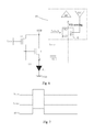
- FIG. 1 which is a 2T1C pixel driving circuit employed for OLED, comprising a first thin film transistor T 10 , a second thin film transistor T 20 and a capacitor C 10 .
- the first thin film transistor T 10 is a switch thin film transistor
- the second thin film transistor T 20 is a drive thin film transistor
- the capacitor C 10 is a storage capacitor.
- a gate of the first thin film transistor T 10 receiving a scan signal Scan, and a drain receiving a data signal Data, and a source being electrically coupled to a gate of the second thin film transistor T 20 and one end of the capacitor C 10 ; a drain of the second thin film transistor T 20 receiving the power source voltage OVDD, and a source being electrically coupled to an anode of the organic light emitting diode D 10 ; a cathode of the organic light emitting diode D 10 receiving a common ground voltage OVSS; one end of the capacitor C 10 being electrically coupled to the gate of the second thin film transistor T 20 , and the other end being electrically coupled to a source of the second thin film transistor T 20 .
- the scan signal Scan controls the first thin film transistor T 10 to be activated, and the data signal Data enters the gate of the second thin film transistor T 20 and the capacitor C 10 via the first thin film transistor T 10 . Then, the first thin film transistor T 10 is deactivated. With the storage function of the capacitor C 10 , the gate voltage of the second thin film transistor T 20 can remain to hold the data signal voltage to make the second thin film transistor T 20 to be in the conducted state to drive the current to enter the organic light emitting diode D 10 via the second thin film transistor T 20 and to drive the organic light emitting diode D 10 to emit light.
- I OLED K ⁇ ( Vgs ⁇ Vth ) 2
- I OLED represents a current flowing through the driving thin film transistor and the organic light emitting diode
- K is an intrinsic conductive factor of the driving thin film transistor
- Vgs represents a voltage difference between the gate and the source of the driving thin film transistor
- Vth represents a threshold voltage of the driving thin film transistor. Accordingly, the value of the I OLED is relevant with the threshold voltage Vth of the driving thin film transistor.
- the structure of the foregoing traditional OLED pixel driving circuit is simpler and does not possess compensation function, and thus lots of defects exist, wherein the more obvious one is: due to the nonconsistency in the manufacture process of the thin film transistor, the threshold voltages of the driving thin film transistors of all pixels in the OLED display device are not consistent; and the long period of working time will age the material of the driving thin film transistors to lead to the drifts of the threshold voltages of the driving thin film transistors and the to cause the phenomenon of the nonuniform display.
- FIG. 2 shows a 3T1C structure OLED pixel driving circuit with compensation function according to prior art.
- a third thin film transistor T 30 is added, and a gate of the third thin film transistor T 30 receives a sensing control signal Sense, and a source is electrically coupled to a source of the second thin film transistor T 20 , and a drain is electrically coupled to a analog to digital converter and receives a reference voltage signal Vref, and a data signal Data is provided by a digital to analog converter.
- the OLED pixel driving circuit of 3T1C structure can sense the threshold voltage Vth of the driving thin film transistor, and compensate the Vth value to the data signal Data, which can eliminate the influence of the threshold voltage Vth of the driving thin film transistor to the current I OLED flowing through the organic light emitting diode, and thus to make the display uniform to improve the image quality.
- the OLED pixel driving circuit of 3T1C structure has drawbacks:
- the reference voltage signal Vref provides the reference voltages to the respective pixels, and the wiring causes the aperture of the pixel decrease.
- the generation of the reference voltage signal Vref increases the channel amount of the driving IC to increase the manufacture cost.
- An objective of the present invention is to provide an OLED pixel driving circuit, which does not only have compensation function but also can eliminate the influence of the threshold voltage of the driving thin film transistor to the current flowing through the organic light emitting diode to promote the display uniformity and to raise the aperture ratio of the pixel for reducing the manufacture cost.
- Another objective of the present invention is to provide an OLED display device, of which the pixel driving circuit possesses compensation function, and the display uniformity is better, and the aperture ratio of the pixel is higher, and the manufacture cost is lower.
- the present invention first provides an OLED pixel driving circuit, comprising a first thin film transistor, a second thin film transistor, a third thin film transistor, a capacitor, an organic light emitting diode, and a switch, a digital to analog converter and an analog to digital converter located inside a driving IC; operating states of the OLED pixel driving circuit including a display mode and a sensing mode;
- the switch being controlled by a switch signal and comprising a first pin, a second pin and a third pin;
- a gate of the first thin film transistor receiving a scan signal, and a drain receiving a power source voltage, and a source being electrically coupled to a gate of the second thin film transistor and one end of the capacitor; a drain of the second thin film transistor receiving the power source voltage, and a source being electrically coupled to an anode of the organic light emitting diode; a cathode of the organic light emitting diode receiving a common ground voltage; the other end of the capacitor being electrically coupled to a source of the second thin film transistor; a gate of the third thin film transistor receiving the scan signal in the display mode and receiving a sensing control signal in the sensing mode, and a source being electrically coupled to the source of the second thin film transistor, and a drain being electrically coupled to the first pin of the switch;
- the second pin of the switch being electrically coupled to the digital to analog converter, and the third pin being electrically coupled to the analog to digital converter;
- the switch signal controlling the switch to connect the first pin and the second pin, and the digital to analog converter providing a data signal; in the sensing mode, the digital to analog converter first providing a low voltage level signal, and then the switch signal controlling the switch to connect the first pin and the third pin to make the analog to digital converter sense a threshold voltage of the second thin film transistor.
- a voltage level of the data signal is not higher than a threshold voltage of the organic light emitting diode, and the power source voltage is higher than a sum of the threshold voltage of the organic light emitting diode and the threshold voltage of the second thin film transistor.
- the threshold voltage of the organic light emitting diode is 10V.
- the scan signal first provides a high voltage level pulse, and maintains a low voltage level; the common ground voltage constantly is the low voltage level; the data signal begins to be a high voltage level, constantly from a rising edge of the high voltage level pulse of the scan signal;
- the scan signal first provides the high voltage level pulse, and maintains the low voltage level;
- the sensing control signal first provides a high voltage level pulse synchronized with the high voltage level pulse of the scan signal, and maintains the low voltage level.
- the common ground voltage first provides a high voltage level pulse synchronized with the high voltage level pulse of the sensing control signal and maintains the low voltage level.
- the present invention further provides an OLED display device, comprising an OLED pixel driving circuit, and the OLED pixel driving circuit comprising a first thin film transistor, a second thin film transistor, a third thin film transistor, a capacitor, an organic light emitting diode, and a switch, a digital to analog converter and an analog to digital converter located inside a driving IC; operating states of the OLED pixel driving circuit including a display mode and a sensing mode;
- the switch being controlled by a switch signal and comprising a first pin, a second pin and a third pin;
- a gate of the first thin film transistor receiving a scan signal, and a drain receiving a power source voltage, and a source being electrically coupled to a gate of the second thin film transistor and one end of the capacitor; a drain of the second thin film transistor receiving the power source voltage, and a source being electrically coupled to an anode of the organic light emitting diode; a cathode of the organic light emitting diode receiving a common ground voltage; the other end of the capacitor being electrically coupled to a source of the second thin film transistor; a gate of the third thin film transistor receiving the scan signal in the display mode and receiving a sensing control signal in the sensing mode, and a source being electrically coupled to the source of the second thin film transistor, and a drain being electrically coupled to the first pin of the switch;
- the second pin of the switch being electrically coupled to the digital to analog converter, and the third pin being electrically coupled to the analog to digital converter;
- the switch signal controlling the switch to connect the first pin and the second pin, and the digital to analog converter providing a data signal; in the sensing mode, the digital to analog converter first providing a low voltage level signal, and then the switch signal controlling the switch to connect the first pin and the third pin to make the analog to digital converter sense a threshold voltage of the second thin film transistor.
- a voltage level of the data signal is not higher than a threshold voltage of the organic light emitting diode, and the power source voltage is higher than a sum of the threshold voltage of the organic light emitting diode and the threshold voltage of the second thin film transistor.
- the threshold voltage of the organic light emitting diode is 10V.
- the scan signal first provides a high voltage level pulse, and maintains a low voltage level; the common ground voltage constantly is the low voltage level; the data signal begins to be a high voltage level, constantly from a rising edge of the high voltage level pulse of the scan signal;
- the scan signal first provides the high voltage level pulse, and maintains the low voltage level;
- the sensing control signal first provides a high voltage level pulse synchronized with the high voltage level pulse of the scan signal, and maintains the low voltage level.
- the common ground voltage first provides a high voltage level pulse synchronized with the high voltage level pulse of the sensing control signal and maintains the low voltage level.
- the present invention further provides an OLED pixel driving circuit, comprising a first thin film transistor, a second thin film transistor, a third thin film transistor, a capacitor, an organic light emitting diode, and a switch, a digital to analog converter and an analog to digital converter located inside a driving IC; operating states of the OLED pixel driving circuit including a display mode and a sensing mode;
- the switch being controlled by a switch signal and comprising a first pin, a second pin and a third pin;
- a gate of the first thin film transistor receiving a scan signal, and a drain receiving a power source voltage, and a source being electrically coupled to a gate of the second thin film transistor and one end of the capacitor; a drain of the second thin film transistor receiving the power source voltage, and a source being electrically coupled to an anode of the organic light emitting diode; a cathode of the organic light emitting diode receiving a common ground voltage; the other end of the capacitor being electrically coupled to a source of the second thin film transistor; a gate of the third thin film transistor receiving the scan signal in the display mode and receiving a sensing control signal in the sensing mode, and a source being electrically coupled to the source of the second thin film transistor, and a drain being electrically coupled to the first pin of the switch;
- the second pin of the switch being electrically coupled to the digital to analog converter, and the third pin being electrically coupled to the analog to digital converter;
- the switch signal controlling the switch to connect the first pin and the second pin, and the digital to analog converter providing a data signal
- the digital to analog converter in the sensing mode, the digital to analog converter first providing a low voltage level signal, and then the switch signal controlling the switch to connect the first pin and the third pin to make the analog to digital converter sense a threshold voltage of the second thin film transistor
- a voltage level of the data signal is not higher than a threshold voltage of the organic light emitting diode, and the power source voltage is higher than a sum of the threshold voltage of the organic light emitting diode and the threshold voltage of the second thin film transistor;
- the threshold voltage of the organic light emitting diode is 10V
- the scan signal first provides a high voltage level pulse, and maintains a low voltage level;
- the common ground voltage constantly is the low voltage level;
- the data signal begins to be a high voltage level, constantly from a rising edge of the high voltage level pulse of the scan signal;
- the scan signal first provides the high voltage level pulse, and maintains the low voltage level;
- the sensing control signal first provides a high voltage level pulse synchronized with the high voltage level pulse of the scan signal, and maintains the low voltage level.
- the present invention provides the OLED pixel driving circuit and the OLED display device, which adds the third thin film transistor and arranges the switch on the basis of the 2T1C structure.
- the first pin of the switch is electrically coupled to the drain of the third thin film transistor, and the second pin is electrically coupled to the digital to analog converter, and the third pin is electrically coupled to the analog to digital converter.
- the switch signal is used to control the switch to connect the first pin and the second pin for entering the display mode
- the switch signal is used to control the switch to connect the first pin and the third pin for entering the sensing mode so that the analog to digital converter can sense the threshold voltage of the second thin film transistor to be employed for the data compensation in the display mode after the analog to digital conversion for possessing the compensation function to eliminate the influence of the threshold voltage of the driving thin film transistor to the current flowing through the organic light emitting diode and to promote the uniformity of the display, and the additional arrangement of the reference voltage signal like prior art is not required to raise the aperture ratio of the pixel and to reduce the manufacture cost.
- FIG. 1 is a circuit diagram of a 2T1C pixel driving circuit used for an OLED according to prior art
- FIG. 2 is a circuit diagram of a 3T1C structure OLED pixel driving circuit with compensation function according to prior art
- FIG. 3 is a circuit diagram of an OLED pixel driving circuit according to the present invention.
- FIG. 4 is a circuit connection diagram of an OLED pixel driving circuit according to the present invention in a display mode
- FIG. 5 is a sequence diagram of an OLED pixel driving circuit according to the present invention in a display mode
- FIG. 6 is a circuit connection diagram of an OLED pixel driving circuit according to the present invention in a sensing mode
- FIG. 7 is a sequence diagram of an OLED pixel driving circuit according to the present invention in a sensing mode.
- the present invention provides an OLED pixel driving circuit.
- the OLED pixel driving circuit of the present invention comprises a first thin film transistor T 1 , a second thin film transistor T 2 , a third thin film transistor T 3 , a capacitor C 1 , an organic light emitting diode D 1 , and a switch K, a digital to analog converter DAC and an analog to digital converter ADC located inside a driving IC 10 .
- the second thin film transistor T 2 is the driving thin film transistor which directly drives the organic light emitting diode D 1 .
- the OLED pixel driving circuit is added with the third thin film transistor T 3 and configured with the switch K, and the operating states includes a display mode and a sensing mode.
- the switch K is controlled by a switch signal Switch, and comprises a first pin K 1 , a second pin K 2 and a third pin K 3 ;
- a gate of the first thin film transistor T 1 receiving a scan signal Scan, and a drain receiving a power source voltage OVDD, and a source being electrically coupled to a gate of the second thin film transistor T 2 and one end of the capacitor C 1 ; a drain of the second thin film transistor T 2 receiving the power source voltage OVDD, and a source being electrically coupled to an anode of the organic light emitting diode D 1 ; a cathode of the organic light emitting diode D 1 receiving a common ground voltage OVSS; the other end of the capacitor C 1 being electrically coupled to a source of the second thin film transistor T 2 ; a gate of the third thin film transistor T 3 receiving the scan signal Scan in the display mode and receiving a sensing control signal Sense in the sensing mode, and a source being electrically coupled to the source of the second thin film transistor T 2 , and a drain being electrically coupled to the first pin K 1 of the switch K;
- the second pin K 2 of the switch K being electrically coupled to the digital to analog converter DAC, and the third pin K 3 being electrically coupled to the analog to digital converter ADC.
- All of the first thin film transistor T 1 , the second thin film transistor T 2 and the third thin film transistor T 3 are low temperature poly-silicon thin film transistors, oxide semiconductor thin film transistors or amorphous silicon thin film transistors.
- the switch signal Switch controls the switch K to connect the first pin K 1 and the second pin K 2
- the digital to analog converter DAC provides the data signal Data.
- the scan signal Scan first provides a high voltage level pulse so that both the first thin film transistor T 1 and the third thin film transistor T 3 are on.
- the power source voltage OVDD enters the gate g of the second thin film transistor T 2 via the first thin film transistor T 1 which is on, i.e.
- the scan signal Scan maintains a low voltage level to make the first thin film transistor T 1 and the third thin film transistor T 3 be off, and relying on the storage function of the capacitor C 1 , the organic light emitting diode D 1 emits light and performs display.
- the common ground voltage OVSS constantly is the low voltage level; a voltage level V Data of the data signal Data is not higher than a threshold voltage Vth- OLED of the organic light emitting diode D 1 , i.e.
- the threshold voltage Vth- OLED of the organic light emitting diode D 1 is about 10V (for an organic light emitting diode having three or four light emitting layers), thus, it can ensures that the voltage level Vs of the source s of the second thin film transistor T 2 cannot light up the organic light emitting diode D 1 in the process of writing the Data signal Data;
- the scan signal Scan first provides a high voltage level to make the first thin film transistor T 1 on, and the power source voltage OVDD enters the gate g of the second thin film transistor T 2 via the first thin film transistor T 1 which is on, i.e.
- the sensing control signal Sense first provides a high voltage level pulse synchronized with the high voltage level pulse of the scan signal Scan to make the third thin film transistor T 3 on
- the switch signal Switch first maintains the switch K to connect the first pin K 1 and the second pin K 2
- the digital to analog converter DAC first provides a low voltage level signal to be written into the source s of the second thin film transistor T 2 via the first pin K 1 and the second pin K 2 of the switch K, and the third thin film transistor T 3 which is on, and meanwhile, the common ground voltage OVSS first provides a high voltage level pulse synchronized with the high voltage level pulse of the sensing control signal Sense to ensure that the organic light emitting diode D 1 cannot be lighted up.
- the switch signal Switch controls the switch K to connect the first pin K 1 and the third pin K 3 .
- the voltage level of the gate g of the second thin film transistor T 2 is OVDD, and the source s is at a lower voltage level, and the analog to digital converter ADC can sense the threshold voltage Vth of the second thin film transistor T 2 , i.e. the driving thin film transistor via the third thin film transistor T 3 which is on, and the first pin K 1 and the third pin K 3 of the switch K.
- all the scan signal Scan, the sensing control signal Sense and the common ground voltage OVSS are transferred to be low voltage levels and maintain the same.
- the analog to digital converter ADC senses the threshold voltage Vth of the second thin film transistor T 2 , i.e. the driving thin film transistor, and then converts the same into the digital sensing data, and saves the digital sensing data for the data compensation in the display mode.
- the threshold voltage Vth of the second thin film transistor T 2 i.e. the driving thin film transistor is compensated, and the current flowing through the organic light emitting diode D 1 is irrelevant with the threshold voltage Vth of the driving thin film transistor to eliminate the influence of the threshold voltage of the driving thin film transistor to the current flowing through the organic light emitting diode D 1 to promote the uniformity of the display and raise the luminescence efficiency.
- the OLED pixel driving circuit of the present invention does not need the additional arrangement of the reference voltage signal as prior arts do, and then omits the wiring of the reference voltage signal to decrease the channel amount of the driving IC and to raise the aperture ratio of the pixel to reduce the manufacture cost.
- the present invention further provides an OLED display device, comprising the aforesaid OLED pixel driving circuit.
- OLED display device comprising the aforesaid OLED pixel driving circuit.
- the descriptions of the structure and the function of the OLED pixel driving circuit are not repeated here.
- the OLED pixel driving circuit and the OLED display device of the present invention adds the third thin film transistor and arranges the switch on the basis of the 2T1C structure.
- the first pin of the switch is electrically coupled to the drain of the third thin film transistor, and the second pin is electrically coupled to the digital to analog converter, and the third pin is electrically coupled to the analog to digital converter.
- the switch signal is used to control the switch to connect the first pin and the second pin for entering the display mode
- the switch signal is used to control the switch to connect the first pin and the third pin for entering the sensing mode so that the analog to digital converter can sense the threshold voltage of the second thin film transistor to be employed for the data compensation in the display mode after the analog to digital conversion for possessing the compensation function to eliminate the influence of the threshold voltage of the driving thin film transistor to the current flowing through the organic light emitting diode and to promote the uniformity of the display, and the additional arrangement of the reference voltage signal like prior art is not required to raise the aperture ratio of the pixel and to reduce the manufacture cost.
Landscapes
- Engineering & Computer Science (AREA)
- Physics & Mathematics (AREA)
- Computer Hardware Design (AREA)
- General Physics & Mathematics (AREA)
- Theoretical Computer Science (AREA)
- Electroluminescent Light Sources (AREA)
- Control Of El Displays (AREA)
- Control Of Indicators Other Than Cathode Ray Tubes (AREA)
Applications Claiming Priority (4)
| Application Number | Priority Date | Filing Date | Title |
|---|---|---|---|
| CN201710104522.X | 2017-02-24 | ||
| CN201710104522.XA CN106652911B (zh) | 2017-02-24 | 2017-02-24 | Oled像素驱动电路及oled显示装置 |
| CN201710104522 | 2017-02-24 | ||
| PCT/CN2017/076778 WO2018152893A1 (zh) | 2017-02-24 | 2017-03-15 | Oled像素驱动电路及oled显示装置 |
Publications (2)
| Publication Number | Publication Date |
|---|---|
| US20180301090A1 US20180301090A1 (en) | 2018-10-18 |
| US10147356B2 true US10147356B2 (en) | 2018-12-04 |
Family
ID=58848361
Family Applications (1)
| Application Number | Title | Priority Date | Filing Date |
|---|---|---|---|
| US15/519,837 Active 2037-05-06 US10147356B2 (en) | 2017-02-24 | 2017-03-15 | OLED pixel driving circuit and OLED display device |
Country Status (3)
| Country | Link |
|---|---|
| US (1) | US10147356B2 (zh) |
| CN (1) | CN106652911B (zh) |
| WO (1) | WO2018152893A1 (zh) |
Families Citing this family (27)
| Publication number | Priority date | Publication date | Assignee | Title |
|---|---|---|---|---|
| CN108877686B (zh) | 2017-05-12 | 2020-12-08 | 京东方科技集团股份有限公司 | 数据补偿方法及装置、显示驱动方法及装置、显示装置 |
| WO2018205615A1 (en) * | 2017-05-12 | 2018-11-15 | Boe Technology Group Co., Ltd. | A data voltage compensation method, a display driving method, and a display apparatus |
| CN107039004B (zh) * | 2017-06-08 | 2019-04-30 | 深圳市华星光电半导体显示技术有限公司 | Amoled显示面板的老化补偿方法 |
| KR102326166B1 (ko) * | 2017-06-30 | 2021-11-16 | 엘지디스플레이 주식회사 | 전계 발광 표시장치와 그 구동방법 |
| CN109326624B (zh) * | 2017-08-01 | 2021-12-24 | 京东方科技集团股份有限公司 | 像素电路、其制造方法及显示装置 |
| US10223972B1 (en) | 2017-09-06 | 2019-03-05 | Shenzhen China Star Optoelectronics Semiconductor Display Technology Co., Ltd. | OLED pixel driving circuit and OLED display device |
| CN107424566B (zh) * | 2017-09-06 | 2019-12-24 | 深圳市华星光电半导体显示技术有限公司 | Oled像素驱动电路及oled显示装置 |
| US10283051B2 (en) | 2017-09-06 | 2019-05-07 | Shenzhen China Star Optoelectronics Semiconductor Display Technology Co., Ltd. | OLED pixel driving circuit and OLED display device |
| CN107424567B (zh) * | 2017-09-06 | 2019-12-24 | 深圳市华星光电半导体显示技术有限公司 | Oled像素驱动电路及oled显示装置 |
| CN107622754B (zh) * | 2017-09-22 | 2023-11-14 | 京东方科技集团股份有限公司 | 像素电路及其控制方法、显示基板、显示装置 |
| CN107808639B (zh) * | 2017-11-07 | 2023-08-01 | 深圳市华星光电半导体显示技术有限公司 | Oled显示装置 |
| US10347182B2 (en) | 2017-11-07 | 2019-07-09 | Shenzhen China Star Optoelectronics Semiconductor Display Technology Co., Ltd. | OLED display device |
| CN107945741A (zh) * | 2017-11-07 | 2018-04-20 | 深圳市华星光电半导体显示技术有限公司 | Oled像素驱动电路、阵列基板及显示装置 |
| CN107767815B (zh) * | 2017-11-30 | 2020-09-29 | 武汉华星光电半导体显示技术有限公司 | Oled显示面板的补偿系统及方法 |
| TWI649741B (zh) * | 2018-01-30 | 2019-02-01 | 友達光電股份有限公司 | 臨界電壓補償電路以及顯示面板 |
| US20190362669A1 (en) * | 2018-05-23 | 2019-11-28 | Wuhan China Star Optoelectronics Semiconductor Display Technology Co., Ltd. | Pixel driving circuit, driving method thereof, and display panel |
| CN108877611B (zh) * | 2018-07-16 | 2019-12-17 | 深圳市华星光电半导体显示技术有限公司 | 像素驱动电路感测方法及像素驱动电路 |
| CN108877685B (zh) * | 2018-07-20 | 2020-05-05 | 深圳市华星光电半导体显示技术有限公司 | 一种oled像素驱动电路及oled显示装置 |
| CN109192142A (zh) * | 2018-09-19 | 2019-01-11 | 深圳市华星光电技术有限公司 | Oled像素驱动电路及驱动方法 |
| TWI708230B (zh) * | 2018-11-20 | 2020-10-21 | 友達光電股份有限公司 | 顯示面板 |
| CN109545134B (zh) * | 2018-11-30 | 2020-07-03 | 昆山国显光电有限公司 | 一种oled显示面板驱动电路及驱动方法 |
| CN109545145B (zh) * | 2019-01-02 | 2020-07-28 | 京东方科技集团股份有限公司 | 像素电路及其驱动方法、显示装置 |
| CN109801597B (zh) * | 2019-02-27 | 2020-12-25 | 深圳市华星光电半导体显示技术有限公司 | 显示器驱动电路及显示器驱动方法 |
| CN110675814B (zh) * | 2019-09-12 | 2021-02-26 | 深圳市华星光电半导体显示技术有限公司 | 一种oled像素补偿电路及像素电路 |
| CN111128069A (zh) * | 2019-11-25 | 2020-05-08 | 南京中电熊猫平板显示科技有限公司 | 一种自发光显示装置以及像素内外补偿兼容电路 |
| CN111415631B (zh) * | 2020-04-28 | 2022-07-12 | Tcl华星光电技术有限公司 | 背光模组和显示设备 |
| CN114814413A (zh) * | 2022-04-11 | 2022-07-29 | 深圳市华星光电半导体显示技术有限公司 | 显示面板及显示面板的老化测试方法 |
Citations (6)
| Publication number | Priority date | Publication date | Assignee | Title |
|---|---|---|---|---|
| KR20100069427A (ko) | 2008-12-16 | 2010-06-24 | 엘지디스플레이 주식회사 | 유기발광다이오드 표시장치 |
| CN103165079A (zh) | 2011-12-12 | 2013-06-19 | 乐金显示有限公司 | 有机发光显示装置及其操作方法 |
| CN104637440A (zh) | 2013-11-06 | 2015-05-20 | 乐金显示有限公司 | 有机发光显示器和补偿其迁移率的方法 |
| CN104658474A (zh) | 2013-11-20 | 2015-05-27 | 乐金显示有限公司 | 有机发光显示器和补偿有机发光显示器的阈值电压的方法 |
| CN104751793A (zh) | 2013-12-26 | 2015-07-01 | 乐金显示有限公司 | 有机发光二极管显示器及感测其驱动特性的方法 |
| CN105489159A (zh) | 2014-10-01 | 2016-04-13 | 乐金显示有限公司 | 有机发光显示装置 |
-
2017
- 2017-02-24 CN CN201710104522.XA patent/CN106652911B/zh active Active
- 2017-03-15 US US15/519,837 patent/US10147356B2/en active Active
- 2017-03-15 WO PCT/CN2017/076778 patent/WO2018152893A1/zh active Application Filing
Patent Citations (6)
| Publication number | Priority date | Publication date | Assignee | Title |
|---|---|---|---|---|
| KR20100069427A (ko) | 2008-12-16 | 2010-06-24 | 엘지디스플레이 주식회사 | 유기발광다이오드 표시장치 |
| CN103165079A (zh) | 2011-12-12 | 2013-06-19 | 乐金显示有限公司 | 有机发光显示装置及其操作方法 |
| CN104637440A (zh) | 2013-11-06 | 2015-05-20 | 乐金显示有限公司 | 有机发光显示器和补偿其迁移率的方法 |
| CN104658474A (zh) | 2013-11-20 | 2015-05-27 | 乐金显示有限公司 | 有机发光显示器和补偿有机发光显示器的阈值电压的方法 |
| CN104751793A (zh) | 2013-12-26 | 2015-07-01 | 乐金显示有限公司 | 有机发光二极管显示器及感测其驱动特性的方法 |
| CN105489159A (zh) | 2014-10-01 | 2016-04-13 | 乐金显示有限公司 | 有机发光显示装置 |
Also Published As
| Publication number | Publication date |
|---|---|
| WO2018152893A1 (zh) | 2018-08-30 |
| US20180301090A1 (en) | 2018-10-18 |
| CN106652911A (zh) | 2017-05-10 |
| CN106652911B (zh) | 2019-03-12 |
Similar Documents
| Publication | Publication Date | Title |
|---|---|---|
| US10147356B2 (en) | OLED pixel driving circuit and OLED display device | |
| US10032838B2 (en) | AMOLED pixel driving circuit and pixel driving method | |
| US10332451B2 (en) | AMOLED pixel driver circuit and pixel driving method | |
| US20210118361A1 (en) | Amoled pixel driving circuit, driving method, and display panel | |
| WO2020015088A1 (zh) | 一种oled像素驱动电路及oled显示装置 | |
| US9824629B2 (en) | AMOLED pixel driving circuit and pixel driving method | |
| US9728131B2 (en) | Five-transistor-one-capacitor AMOLED pixel driving circuit and pixel driving method based on the circuit | |
| US9697775B2 (en) | AMOLED pixel driving circuit and pixel driving method that implements threshold voltage compensation by directly gaining threshold voltage of driving TFT | |
| US20210327347A1 (en) | Pixel circuit and driving method thereof, and display panel | |
| WO2016119304A1 (zh) | Amoled像素驱动电路及像素驱动方法 | |
| CN107424566B (zh) | Oled像素驱动电路及oled显示装置 | |
| WO2018152896A1 (zh) | Oled像素驱动电路及像素驱动方法 | |
| WO2019037300A1 (zh) | Amoled像素驱动电路 | |
| US10056033B2 (en) | AMOLED pixel driving circuit and pixel driving method | |
| CN108777131B (zh) | Amoled像素驱动电路及驱动方法 | |
| US20160314740A1 (en) | Amoled pixel driving circuit and pixel driving method | |
| WO2016119305A1 (zh) | Amoled像素驱动电路及像素驱动方法 | |
| US10223972B1 (en) | OLED pixel driving circuit and OLED display device | |
| CN107424567B (zh) | Oled像素驱动电路及oled显示装置 | |
| US10475385B2 (en) | AMOLED pixel driving circuit and driving method capable of ensuring uniform brightness of the organic light emitting diode and improving the display effect of the pictures | |
| US10424249B2 (en) | Pixel driving circuit and driving method thereof, array substrate, and display device | |
| US10283051B2 (en) | OLED pixel driving circuit and OLED display device | |
| US10074309B2 (en) | AMOLED pixel driving circuit and AMOLED pixel driving method | |
| US10304387B2 (en) | AMOLED pixel driving circuit and AMOLED pixel driving method | |
| WO2018166037A1 (zh) | 一种像素驱动电路及oled显示装置 |
Legal Events
| Date | Code | Title | Description |
|---|---|---|---|
| AS | Assignment |
Owner name: SHENZHEN CHINA STAR OPTOELECTRONICS TECHNOLOGY CO. Free format text: ASSIGNMENT OF ASSIGNORS INTEREST;ASSIGNOR:KUANG, JIMU;REEL/FRAME:042035/0251 Effective date: 20170323 |
|
| AS | Assignment |
Owner name: SHENZHEN CHINA STAR OPTOELECTRONICS SEMICONDUCTOR Free format text: ASSIGNMENT OF ASSIGNORS INTEREST;ASSIGNOR:SHENZHEN CHINA STAR OPTOELECTRONICS TECHNOLOGY CO., LTD.;REEL/FRAME:043748/0827 Effective date: 20170928 |
|
| STCF | Information on status: patent grant |
Free format text: PATENTED CASE |
|
| MAFP | Maintenance fee payment |
Free format text: PAYMENT OF MAINTENANCE FEE, 4TH YEAR, LARGE ENTITY (ORIGINAL EVENT CODE: M1551); ENTITY STATUS OF PATENT OWNER: LARGE ENTITY Year of fee payment: 4 |