US10090161B2 - Plasma etching apparatus and plasma etching method - Google Patents
Plasma etching apparatus and plasma etching method Download PDFInfo
- Publication number
- US10090161B2 US10090161B2 US15/404,471 US201715404471A US10090161B2 US 10090161 B2 US10090161 B2 US 10090161B2 US 201715404471 A US201715404471 A US 201715404471A US 10090161 B2 US10090161 B2 US 10090161B2
- Authority
- US
- United States
- Prior art keywords
- wafer
- outer edge
- plasma
- substrate
- edge portion
- Prior art date
- Legal status (The legal status is an assumption and is not a legal conclusion. Google has not performed a legal analysis and makes no representation as to the accuracy of the status listed.)
- Active
Links
Images


Classifications
-
- H—ELECTRICITY
- H10—SEMICONDUCTOR DEVICES; ELECTRIC SOLID-STATE DEVICES NOT OTHERWISE PROVIDED FOR
- H10P—GENERIC PROCESSES OR APPARATUS FOR THE MANUFACTURE OR TREATMENT OF DEVICES COVERED BY CLASS H10
- H10P50/00—Etching of wafers, substrates or parts of devices
- H10P50/20—Dry etching; Plasma etching; Reactive-ion etching
- H10P50/24—Dry etching; Plasma etching; Reactive-ion etching of semiconductor materials
- H10P50/242—Dry etching; Plasma etching; Reactive-ion etching of semiconductor materials of Group IV materials
-
- H01L21/3065—
-
- H—ELECTRICITY
- H01—ELECTRIC ELEMENTS
- H01J—ELECTRIC DISCHARGE TUBES OR DISCHARGE LAMPS
- H01J37/00—Discharge tubes with provision for introducing objects or material to be exposed to the discharge, e.g. for the purpose of examination or processing thereof
- H01J37/32—Gas-filled discharge tubes
- H01J37/32009—Arrangements for generation of plasma specially adapted for examination or treatment of objects, e.g. plasma sources
- H01J37/32082—Radio frequency generated discharge
- H01J37/32091—Radio frequency generated discharge the radio frequency energy being capacitively coupled to the plasma
-
- H—ELECTRICITY
- H01—ELECTRIC ELEMENTS
- H01J—ELECTRIC DISCHARGE TUBES OR DISCHARGE LAMPS
- H01J37/00—Discharge tubes with provision for introducing objects or material to be exposed to the discharge, e.g. for the purpose of examination or processing thereof
- H01J37/32—Gas-filled discharge tubes
- H01J37/32009—Arrangements for generation of plasma specially adapted for examination or treatment of objects, e.g. plasma sources
- H01J37/32082—Radio frequency generated discharge
- H01J37/32137—Radio frequency generated discharge controlling of the discharge by modulation of energy
- H01J37/32155—Frequency modulation
- H01J37/32165—Plural frequencies
-
- H—ELECTRICITY
- H01—ELECTRIC ELEMENTS
- H01J—ELECTRIC DISCHARGE TUBES OR DISCHARGE LAMPS
- H01J37/00—Discharge tubes with provision for introducing objects or material to be exposed to the discharge, e.g. for the purpose of examination or processing thereof
- H01J37/32—Gas-filled discharge tubes
- H01J37/32431—Constructional details of the reactor
- H01J37/32623—Mechanical discharge control means
- H01J37/32651—Shields, e.g. dark space shields, Faraday shields
-
- H—ELECTRICITY
- H01—ELECTRIC ELEMENTS
- H01J—ELECTRIC DISCHARGE TUBES OR DISCHARGE LAMPS
- H01J37/00—Discharge tubes with provision for introducing objects or material to be exposed to the discharge, e.g. for the purpose of examination or processing thereof
- H01J37/32—Gas-filled discharge tubes
- H01J37/32431—Constructional details of the reactor
- H01J37/32715—Workpiece holder
-
- H01L21/31138—
-
- H01L21/68735—
-
- H01L21/76898—
-
- H—ELECTRICITY
- H10—SEMICONDUCTOR DEVICES; ELECTRIC SOLID-STATE DEVICES NOT OTHERWISE PROVIDED FOR
- H10P—GENERIC PROCESSES OR APPARATUS FOR THE MANUFACTURE OR TREATMENT OF DEVICES COVERED BY CLASS H10
- H10P50/00—Etching of wafers, substrates or parts of devices
- H10P50/20—Dry etching; Plasma etching; Reactive-ion etching
- H10P50/28—Dry etching; Plasma etching; Reactive-ion etching of insulating materials
- H10P50/286—Dry etching; Plasma etching; Reactive-ion etching of insulating materials of organic materials
- H10P50/287—Dry etching; Plasma etching; Reactive-ion etching of insulating materials of organic materials by chemical means
-
- H—ELECTRICITY
- H10—SEMICONDUCTOR DEVICES; ELECTRIC SOLID-STATE DEVICES NOT OTHERWISE PROVIDED FOR
- H10P—GENERIC PROCESSES OR APPARATUS FOR THE MANUFACTURE OR TREATMENT OF DEVICES COVERED BY CLASS H10
- H10P72/00—Handling or holding of wafers, substrates or devices during manufacture or treatment thereof
- H10P72/70—Handling or holding of wafers, substrates or devices during manufacture or treatment thereof for supporting or gripping
- H10P72/76—Handling or holding of wafers, substrates or devices during manufacture or treatment thereof for supporting or gripping using mechanical means, e.g. clamps or pinches
- H10P72/7604—Handling or holding of wafers, substrates or devices during manufacture or treatment thereof for supporting or gripping using mechanical means, e.g. clamps or pinches the wafers being placed on a susceptor, stage or support
- H10P72/7611—Handling or holding of wafers, substrates or devices during manufacture or treatment thereof for supporting or gripping using mechanical means, e.g. clamps or pinches the wafers being placed on a susceptor, stage or support characterised by edge profile or support profile
-
- H—ELECTRICITY
- H10—SEMICONDUCTOR DEVICES; ELECTRIC SOLID-STATE DEVICES NOT OTHERWISE PROVIDED FOR
- H10W—GENERIC PACKAGES, INTERCONNECTIONS, CONNECTORS OR OTHER CONSTRUCTIONAL DETAILS OF DEVICES COVERED BY CLASS H10
- H10W20/00—Interconnections in chips, wafers or substrates
- H10W20/01—Manufacture or treatment
- H10W20/021—Manufacture or treatment of interconnections within wafers or substrates
- H10W20/023—Manufacture or treatment of interconnections within wafers or substrates the interconnections being through-semiconductor vias
- H10W20/0242—Manufacture or treatment of interconnections within wafers or substrates the interconnections being through-semiconductor vias comprising etching via holes from the back sides of the chips, wafers or substrates
-
- H—ELECTRICITY
- H01—ELECTRIC ELEMENTS
- H01J—ELECTRIC DISCHARGE TUBES OR DISCHARGE LAMPS
- H01J2237/00—Discharge tubes exposing object to beam, e.g. for analysis treatment, etching, imaging
- H01J2237/32—Processing objects by plasma generation
- H01J2237/33—Processing objects by plasma generation characterised by the type of processing
- H01J2237/334—Etching
Definitions
- the present invention relates to a plasma etching apparatus and a plasma etching method.
- Semiconductor devices stacked in the vertical direction may include electrodes that are arranged to penetrate through a substrate made of silicon, for example. In this way, the semiconductor devices may be electrically connected via the electrodes.
- a resist is applied on the substrate using a coater, the resist is exposed using an exposure apparatus, and a resist pattern is developed using a developing apparatus. The resist is then used as a mask to etch the substrate using a plasma etching apparatus to create a through hole or a via hole. After creating the through hole or via hole in the substrate, the resist remaining on the substrate is removed by ashing.
- the resist applied on the substrate may come into contact with a substrate carrier or a transfer arm and come off during transfer of the substrate, and this may result in the generation of dust. Accordingly, after applying the resist on the substrate, the resist is removed from the rear surface and the outer edge portion including a bevel portion of the substrate by a back rinse mechanism and a bevel rinse mechanism of the coater using an organic solvent, for example. In this way, dust may be prevented from being generated as a result of the resist coming off of the outer edge portion of the substrate (See e.g., Patent Document 1).
- an insolubilization process may be performed on the resist pattern formed at the outer edge portion of the substrate using a developing solution (See e.g., Patent Document 2).
- Patent Document 1 Japanese Laid-Open Patent Publication No. 2009-295636
- Patent Document 2 Japanese Laid-Open Patent Publication No. 2000-331913
- black silicon refers to the roughening of the silicon substrate surface due to exposure to plasma.
- black silicon may be formed at both the substrate surface and rear surface within this region.
- the region extending over a predetermined width from the outer edge of the substrate may be protected by a resist as illustrated in Patent Documents 1 and 2, for example.
- the resist may come off during transfer of the substrate to result in the generation of dust, for example.
- the above problem is not limited to cases of etching one substrate.
- the adhesive is exposed at the outer edge portion of the bonded substrate.
- the exposed adhesive may come off upon coming into contact with plasma to cause the generation of dust, or the substrates themselves may be separated from one another.
- the outer edge portion of the bonded substrate may become brittle or be prone to cracking, for example.
- the present invention has been conceived in view of the foregoing problems associated with the prior art, and it is an object of the present invention to provide a plasma etching apparatus and a plasma etching method that are capable of protecting the outer edge portion of a substrate having a resist pattern formed thereon upon etching the substrate.
- a plasma etching apparatus that performs plasma etching on a substrate having a surface portion on which a resist pattern is formed and an outer edge portion where a substrate surface of the substrate is exposed.
- the plasma etching apparatus includes a support part that supports the substrate; a cover member that covers the outer edge portion of the substrate that is supported by the support part and prevents plasma from coming around the outer edge portion of the substrate; and a control unit that generates plasma by controlling application of a high frequency power from a high frequency power supply and supply of a processing gas for etching from a first processing gas supply source, and uses the generated plasma to etch the substrate that is supported by the support part and has the outer edge portion covered by the cover member.
- control unit After etching the substrate, the control unit generates plasma by controlling application of a high frequency power from a high frequency power supply and supply of a processing gas for ashing from a second processing gas supply source, and uses the generated plasma to perform ashing on the resist pattern on the etched substrate.
- a plasma etching apparatus that performs plasma etching on a bonded substrate, which includes a plurality of substrates that are bonded together via an adhesive, the bonded substrate having a surface portion on which a resist pattern is formed and an outer edge portion where the adhesive is exposed.
- the plasma etching apparatus includes a support part that supports the bonded substrate; a cover member that covers the outer edge portion of the bonded substrate that is supported by the support part and prevents plasma from coming around the outer edge portion of the bonded substrate; and a control unit that generates plasma by controlling application of a high frequency power from a high frequency power supply and supply of a processing gas for etching from a first processing gas supply source, and uses the generated plasma to etch the bonded substrate that is supported by the support part and has the outer edge portion covered by the cover member.
- control unit After etching the bonded substrate, the control unit generates plasma by controlling application of a high frequency power from a high frequency power supply and supply of a processing gas for ashing from a second processing gas supply source, and uses the generated plasma to perform ashing on the resist pattern on the etched bonded substrate.
- a plasma etching method for performing plasma etching on a substrate having a surface portion on which a resist pattern is formed and an outer edge portion where a substrate surface of the substrate is exposed.
- the plasma etching method includes the steps of supporting the substrate by a support part; arranging a cover member to cover the outer edge portion of the substrate that is supported by the support part to prevent plasma from coming around the outer edge portion of the substrate; generating plasma by controlling application of a high frequency power from a high frequency power supply and controlling supply of a processing gas for etching from a first processing gas supply source, and using the generated plasma to etch the substrate that is supported by the support part and has the outer edge portion covered by the cover member; and after etching the substrate, generating plasma by controlling application of a high frequency power from a high frequency power supply and controlling supply of a processing gas for ashing from a second processing gas supply source, and using the generated plasma to perform ashing on the resist pattern on the etched substrate.
- a plasma etching method for performing plasma etching on a bonded substrate, which includes a plurality of substrates that are bonded together via an adhesive, the bonded substrate having a surface portion on which a resist pattern is formed and an outer edge portion where the adhesive is exposed.
- the plasma etching method includes the steps of supporting the bonded substrate by a support part; arranging a cover member to cover the outer edge portion of the bonded substrate that is supported by the support part to prevent plasma from coming around the outer edge portion of the bonded substrate; generating plasma by controlling application of a high frequency power from a high frequency power supply and controlling supply of a processing gas for etching from a first processing gas supply source, and using the generated plasma to etch the bonded substrate that is supported by the support part and has the outer edge portion covered by the cover member; and after etching the bonded substrate, generating plasma by controlling application of a high frequency power from a high frequency power supply and controlling supply of a processing gas for ashing from a second processing gas supply source, and using the generated plasma to perform ashing on the resist pattern on the etched bonded substrate.
- an outer edge portion of the substrate when etching a substrate having a resist pattern formed thereon, an outer edge portion of the substrate may be protected.
- FIG. 1 is a schematic cross-sectional view illustrating a configuration of a plasma etching apparatus according to a first embodiment of the present invention
- FIG. 2 is an enlarged cross-sectional view of a portion surrounding a bevel cover ring
- FIG. 3 is a schematic cross-sectional view illustrating a first state of an operation for placing a wafer on an electrostatic chuck
- FIG. 4 is a schematic cross-sectional view illustrating a second state of the operation for placing the wafer on the electrostatic chuck
- FIG. 5 is a schematic cross-sectional view illustrating a third state of the operation for placing the wafer on the electrostatic chuck
- FIG. 6 is a schematic cross-sectional view illustrating a fourth state of the operation for placing the wafer on the electrostatic chuck
- FIG. 7 is an enlarged cross-sectional view illustrating the wafer being supported by the electrostatic chuck while having an outer edge portion covered by a brim part of an upper ring member;
- FIG. 8 is a cross-sectional view illustrating surface roughening of a substrate surface of the wafer at its outer edge portion that may occur in a case where the outer edge portion is not covered by the upper ring member;
- FIG. 9 is a cross-sectional view illustrating an inclination of a via hole formed within the wafer
- FIG. 10 is a graph indicating measurement results of inclination angles with respect to the vertical direction of via holes formed at various distances from the outer edge of the wafer;
- FIG. 11 is a graph indicating measurement results of resist ashing rates at various points on the wafer at various distances from the outer edge of the wafer in two different examples using different ashing conditions;
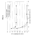
- FIG. 12 is a graph indicating measurement results of resist film thicknesses before and after ashing at various points on the wafer at various distances from the outer edge of the wafer;
- FIG. 13 is a schematic cross-sectional view illustrating a configuration of a bonded wafer
- FIG. 14A is a schematic cross-sectional view illustrating a first state of a wafer in a process step of a semiconductor device manufacturing method including a plasma etching method according to a second embodiment of the present invention
- FIG. 14B is a schematic cross-sectional view illustrating a second state of the wafer in a process step of the semiconductor device manufacturing method including the plasma etching method according to the second embodiment;
- FIG. 14C is a schematic cross-sectional view illustrating a third state of the wafer in a process step of the semiconductor device manufacturing method including the plasma etching method according to the second embodiment;
- FIG. 15A is a schematic cross-sectional view illustrating a fourth state of the wafer in a process step of the semiconductor device manufacturing method including the plasma etching method according to the second embodiment;
- FIG. 15B is a schematic cross-sectional view illustrating a fifth state of the wafer in a process step of the semiconductor device manufacturing method including the plasma etching method according to the second embodiment;
- FIG. 15C is a schematic cross-sectional view illustrating a sixth state of the wafer in a process step of the semiconductor device manufacturing method including the plasma etching method according to the second embodiment.
- FIG. 16 is a table indicating measurement results of the angles of via holes with respect to the horizontal direction for via holes formed at various distances from the center of the wafer.
- FIG. 1 is a schematic cross-sectional view illustrating a configuration of the plasma etching apparatus according to the first embodiment of the present invention.
- the plasma etching apparatus includes a processing chamber 1 that is configured to be airtight and is electrically grounded.
- the processing chamber 1 has a cylindrical structure and may be made of aluminum, for example.
- a stage 2 that holds a semiconductor wafer W (simply referred to as “wafer W” hereinafter) in the horizontal direction is arranged inside the processing chamber 1 .
- the wafer W is an example of a substrate to be processed.
- the stage 2 may be made of aluminum, for example, and is configured to act as a lower electrode.
- the stage 2 is supported by a conductor support 4 and is arranged at a bottom of the processing chamber 1 via an insulating plate 3 .
- a cylindrical inner wall member 3 a that may be made of quartz, for example, is arranged to surround the stage 2 and the support 4 .
- a bevel cover ring 5 is arranged on an upper side outer edge portion of the stage 2 .
- the configuration of the bevel cover ring 5 is described in detail below.
- the bevel cover ring 5 is an embodiment of a cover member that prevents plasma from coming around the outer edge portion of a substrate.
- a first RF power supply 10 a is connected to the stage 2 via a first matching unit 11 a
- a second RF power supply 10 b is connected to the stage 2 via a second matching unit 11 b
- the first RF power supply 10 a is for plasma generation.
- the first RF power supply 10 a is configured to output to the stage 2 a high frequency power of a predetermined frequency (at least 27 MHz; e.g., 100 MHz).
- the second RF power supply 10 b is for ion attraction.
- the second RF power supply 10 b is configured to output to the stage 2 a high frequency power of a predetermined frequency (no more than 13.56 MHz; e.g., 13.56 MHz) that is lower than the high frequency power output by the first RF power supply 10 a .
- a shower head 16 that acts as an upper electrode is arranged above the stage 2 to face the stage 2 in parallel.
- the shower head 16 and the stage 2 are configured to function as a pair of electrodes (i.e., upper electrode and lower electrode).
- plasma is generated from a processing gas for etching that is introduced from the shower head 16 , which acts as the upper electrode, using the high frequency power applied to the stage 2 , which acts as the lower electrode.
- the generated plasma is used to perform an etching process on the wafer W that has its outer edge portion covered by the cover member (bevel cover ring 5 ).
- plasma is generated from a processing gas for ashing that is introduced into the processing chamber 1 by the high frequency power applied to the lower electrode, and the generated plasma is used to perform an ashing process on the wafer W that has its outer edge portion covered by the cover member.
- the above processes are controlled by a control unit 90 .
- An electrostatic chuck 6 that is configured to hold the wafer W by an electrostatic attracting force is provided on a top surface of the stage 2 .
- the electrostatic chuck 6 includes an electrode 6 a arranged within an insulator 6 b .
- the electrode 6 a is electrically connected to a DC power supply 12 .
- a Coulomb force is generated between the electrode 6 a and the wafer W by the application of a DC voltage from the DC power supply 12 so that the wafer W may be electrostatically attracted to the electrostatic chuck 6 by the Coulomb force. In this way, the wafer W is held by the electrostatic chuck 6 .
- the stage 2 and the electrostatic chuck 6 embody a support part that supports a substrate.
- a coolant path 4 a is formed within the support 4 , and the coolant path 4 a is connected to a coolant inlet pipeline 4 b and a coolant outlet pipeline 4 c .
- a suitable coolant such as cooling water
- the support 4 and the stage 2 may be controlled to a predetermined temperature.
- a rear side gas supply line 30 for supplying a heat transfer gas (rear side gas) such as a helium (He) gas to a rear surface of the wafer W is arranged to penetrate through the stage 2 , for example.
- the rear side gas supply line 30 is connected to a rear side gas supply source (not shown).
- the shower head 16 is arranged at a ceiling portion of the processing chamber 1 .
- the shower head 16 includes a main body 16 a and an upper ceiling plate 16 b , which acts as an electrode plate.
- the shower head 16 is mounted to a top part of the processing chamber 1 via an insulating member 17 .
- the main body 16 a may be made of a conductive material such as aluminum having a surface that is alumite-treated, for example.
- the upper ceiling plate 16 b is detachably mounted to a lower part of the main body 16 a.
- the main body 16 a has a gas diffusion chamber 16 c arranged therein. Multiple gas through holes 16 d that communicate with the gas diffusion chamber 16 c are arranged at a bottom part of the main body 16 a . Also, gas introduction holes 16 e that communicate with the gas through holes 16 d are arranged to penetrate through the upper ceiling plate 16 b in its thickness direction. With such an arrangement, a processing gas supplied to the gas diffusion chamber 16 c may be dispersed via the gas through holes 16 d and the gas introduction holes 16 e upon being supplied to the processing chamber 1 . Further, a pipeline (not shown) for circulating a coolant is arranged within the main body 16 a so that the shower head 16 may be cooled to a predetermined temperature while a plasma etching process is performed.
- the main body 16 a has a gas introduction port 16 f for introducing processing gas for etching into the gas diffusion chamber 16 c .
- the gas introduction port 16 f is connected to one end of a gas supply pipeline 14 a .
- the other end of the gas supply pipeline 14 a is connected to a first processing gas supply source 14 for supplying the processing gas for etching.
- a mass flow controller (MFC) 14 b and an open/close valve V 1 are arranged on the gas supply line 14 a in this order from the upstream side.
- Processing gas for plasma etching is introduced into the gas diffusion chamber 16 c from the first processing gas supply source 14 via the gas supply pipeline 14 a .
- the processing gas is then discharged from the gas diffusion chamber 16 c through the gas through holes 16 d and the gas introduction holes 16 e to be dispersed into the processing chamber 1 like a shower.
- the main body 16 a also has a gas introduction port 16 g for introducing processing gas for ashing into the gas diffusion chamber 16 c .
- the gas introduction port 16 g is connected to one end of a gas supply pipeline 15 a .
- the other end of the gas supply pipeline 15 a is connected to a second processing gas supply source 15 that supplies a processing gas for ashing.
- a mass flow controller (MFC) 15 b and an open/close valve V 2 are arranged on the gas supply line 15 a in this order from the upstream side.
- Processing gas for plasma ashing is introduced into the gas diffusion chamber 16 c from the second processing gas supply source 15 via the gas supply pipeline 15 a .
- the processing gas is then discharged from the gas diffusion chamber 16 c through the gas through holes 16 d and the gas introduction holes 16 e to be dispersed into the processing chamber 1 like a shower.
- the shower head 16 which acts as the upper electrode as described above, is electrically connected to a low pass filter (LPF) 71 via a variable DC power supply 72 .
- Power supply operations of the variable DC power supply 72 may be turned on/off by an on/off switch 73 .
- the current voltage of the variable DC power supply 72 and the on/off operations of the on/off switch 73 are controlled by the control unit 90 (described below).
- the control unit 90 when generating plasma within the processing chamber 1 by applying a high frequency power from the first RF power supply 10 a or the second RF power supply 10 b to the stage 2 , the control unit 90 turns on the on/off switch 73 as is necessary so that a predetermined DC voltage may be applied to the shower head 16 , which acts as the upper electrode.
- a cylindrically-shaped ground conductor 1 a is arranged to extend above the height of the shower head 16 from the side wall of the processing chamber 1 .
- the cylindrically-shaped ground conductor 1 a has a ceiling wall arranged at its top portion.
- An exhaust port 81 is formed at a bottom portion of the processing chamber 1 , and an exhaust device 83 is connected to the exhaust port 81 via an exhaust pipe 82 .
- the exhaust device 83 includes a vacuum pump, and the pressure within the processing chamber 1 may be reduced to a predetermined degree of vacuum by operating this vacuum pump.
- a loading/unloading port 84 is arranged at the side wall of the processing chamber 1 , and a gate valve 85 , which is configured to open and close the loading/unloading port 84 , is arranged at the loading/unloading port 84 .
- deposition shields 86 and 87 which are configured to be detachable, are arranged within the processing chamber 1 .
- the deposition shield 86 is arranged along the inner wall face of the processing chamber 1 and is configured to prevent etching by-products (deposition) from adhering to the processing chamber 1 .
- a conductive member (GND block) 89 is connected to the deposition shield 86 at a height position that is substantially the same as that of the wafer W.
- the conductive member (GND block) 89 is connected such that its potential with respect to ground may be controlled, and in this way, an abnormal discharge may be prevented.
- FIG. 2 is an enlarged schematic cross-sectional view of a portion surrounding the bevel cover ring 5 .
- the bevel cover ring 5 includes an upper ring member 51 , a lower ring member 52 , a lift pin 53 , and a drive mechanism 54 .
- the upper ring member 51 includes a main part 51 a and a brim part 51 b .
- the main part 51 a has a ring-shaped structure.
- the brim part 51 b is arranged to protrude inward from the inner circumference of the main part 51 a in the radial direction of the ring-shaped main part 51 a .
- the brim part 51 b is configured to cover an outer edge portion WE of the wafer W that is held by the electrostatic chuck 6 .
- the upper ring member 51 includes the brim part 51 b that covers the outer edge portion WE in order to prevent plasma from coming around the outer edge portion WE of the wafer W.
- the upper ring member 51 may be made of quartz or yttria (Y 2 O 3 ), for example. Yttria may be preferred considering its excellent plasma resistance. Also, as described in detail below with reference to FIG. 16 , in terms of suppressing the inclination angle of a via hole V, yttrium may produce effects that are substantially the same or even more advantageous than that in a case where quartz is used.
- the lower ring member 52 is arranged into a ring-shaped structure corresponding to the ring-shape of the upper ring member 51 .
- a ring-shaped groove 52 a is formed at the upper face of the lower ring member 52 .
- the lower ring member 52 may be made of quartz, for example.
- holes 51 d are formed at the bottom faces of the protrusions 51 c of the upper ring member 51 .
- the lift pin 53 is arranged within a hole 6 c formed at the electrostatic chuck 6 at a position corresponding to that of the hole 51 d , which is formed at the upper ring member 51 .
- the lift pin 53 is configured to be movable in the vertical direction by the drive mechanism 54 that drives the lift pin 53 to move up and down.
- the drive mechanism 54 that drives the lift pin 53 to move up and down.
- the electrostatic chuck 6 includes a lift pin 61 and a drive mechanism 62 .
- the lift pin 61 is arranged within a hole 6 d formed at the electrostatic chuck 6 and is configured to be movable in the vertical direction by the drive mechanism 62 that drives the lift pin 61 to move up and down.
- the drive mechanism 62 drives the lift pin 61 to move up and down.
- the control unit 90 includes a process controller 91 , a user interface 92 , and a storage unit 93 .
- the process controller 91 includes a CPU and is configured to control operations of various components of the plasma etching device.
- the user interface 92 may include a keyboard that is operated by a process controller to input various commands for controlling the process of the plasma etching apparatus, and a display that indicates the operation status of the plasma etching apparatus in visual form, for example.
- the storage unit 93 stores recipes that include control programs (software) for enabling the process controller 91 to control various process operations of the plasma etching apparatus and process condition data, for example.
- the process controller 91 reads a given recipe from the storage unit 93 according to a command from the user interface 92 to execute a desired process. In this way, the plasma etching apparatus may perform the desired process under control by the control processor 91 .
- the recipes including the control programs and process condition data may be stored in a computer-readable storage medium (e.g., hard disk, CD, flexible disk, semiconductor memory). In other embodiments, the recipes including the control programs and process condition data may be transmitted from another device via a dedicated line, for example.
- FIGS. 3-6 are schematic cross-sectional views illustrating various states of an operation for placing the wafer W on the electrostatic chuck 6 .
- the lift pin 53 is raised by the drive mechanism 54 in a state where the wafer W is not held by the electrostatic chuck 6 (see FIG. 3 ).
- the raised lift pin 53 pushes the upper ring member 51 upward to raise the upper ring member 51 (see FIG. 4 ).
- the gate valve 85 is opened, and the wafer W having a resist pattern formed thereon is transferred by a transfer robot (not shown), for example, to be delivered onto the electrostatic chuck 6 within the processing chamber 1 from the loading/unloading port 84 via a load lock chamber (not shown). Then, the lift pin 61 is raised by the drive mechanism 62 , and the wafer W is received by the raised lift pin 61 from the transfer robot (see FIG. 5 ).
- the transfer robot is evacuated out of the processing chamber 1 , and the gate valve 85 is closed. Then, the lift pin 61 is lowered by the drive mechanism 62 , and the wafer W is placed on the electrostatic chuck 6 (see FIG. 6 ). Further, a predetermined DC voltage from the DC power supply 12 is applied to the electrode 6 a of the electrostatic chuck 6 , and as a result the wafer W is electrostatically attracted to the electrostatic chuck 6 by the Coulomb force that is generated between the wafer W and the electrostatic chuck 6 .
- the upper ring member 51 is lowered to its original position to be accommodated within a ring-shaped groove 52 a .
- the wafer W and the bevel cover ring 5 may be in their respective positions illustrated in FIG. 2 .
- the outer edge portion WE of the wafer W may be covered by the brim part 51 b of the upper ring member 51 .
- the wafer W is electrostatically attracted to the electrostatic chuck 6 before the upper ring member 51 is lowered.
- the electrostatic attraction of the wafer W to the electrostatic chuck 6 may alternatively be performed after lowering the upper ring member 51 , for example.
- FIG. 7 is an enlarged cross-sectional view of the wafer W having its outer edge portion WE covered by the brim part 51 b of the upper ring member 51 and being supported by the electrostatic chuck 6 in such a state.
- the upper ring member 51 covers a region of the outer edge portion WE of the wafer W extending over a predetermined width L from the outer edge of the wafer W.
- a resist pattern (resist PR) is formed on the surface of the wafer W.
- the resist PR is removed from a region of the outer edge portion WE of the wafer W extending over a predetermined width L 1 from the outer edge of the wafer W so that the substrate surface of the waver W is exposed at this region.
- the predetermined width L is preferably greater than the predetermined width L 1 . L>L 1 (1)
- the predetermined width L 1 is an example of a first predetermined width that satisfies formula (1).
- DI inner diameter of the upper ring member 51
- DO outer diameter of the wafer W
- the relationship between DI, DO, and L 1 preferably satisfies the following formula (3).
- the etching process involves introducing a predetermined processing gas (etching gas) into the processing chamber 1 from the first processing gas supply source 14 in a state where the processing chamber 1 is depressurized to a predetermined degree of vacuum and maintained at a predetermined pressure.
- a predetermined processing gas etching gas
- the so-called halogen gas such as Cl 2 , Cl 2 +HBr, Cl 2 +O 2 , CF 4 +O 2 , SF 6 , Cl 2 +N 2 , Cl 2 +HCl, or HBr+Cl 2 +SF 6 may be used as the predetermined processing gas, for example.
- a mixed gas including CF gas e.g., CF 4 , C 4 F 8 , CHF 3 , CH 3 F, CH 2 F 2
- Ar gas or a gas having oxygen added to such mixed gas
- a high frequency power of 100 MHz is supplied to the stage 2 from the first RF power supply 10 a .
- a high frequency power (for biasing) of 13.56 MHz is supplied to the stage 2 from the second RF power supply 10 b to prompt ion attraction.
- an electric field is formed between the shower head 16 corresponding to the upper electrode and the stage 2 corresponding to the lower electrode. Electrical discharge occurs within the processing chamber 1 that accommodates the wafer W, and this electrical discharge prompts the generation of plasma from the processing gas. Anisotropic etching is performed on the wafer W by the generated plasma using the resist pattern famed on the surface of the wafer W as a mask while the outer edge portion WE of the wafer W is covered by the upper ring member 51 .
- an ashing process is performed to remove the remaining resist from the wafer W.
- the ashing process is performed using plasma generated from a processing gas for ashing.
- the ashing process involves introducing a predetermined processing gas (ashing gas) into the processing chamber 1 from the second processing gas supply source 15 in a state where the processing chamber 1 is depressurized to a predetermined degree of vacuum and maintained at a predetermined pressure.
- a predetermined processing gas ashing gas
- O 2 gas, NO gas, N 2 O gas, H 2 O gas, or O 3 gas may be used as the predetermined processing gas for ashing.
- a high frequency power of 100 MHz for example, is supplied to the stage 2 from the first RF power supply 10 a .
- a high frequency power (for biasing) of 13.56 MHz is supplied to the stage 2 from the second RF power supply 10 b to prompt ion attraction.
- the application of high frequency power, the application of the DC voltage, and the supply of processing gas are stopped. Then, the wafer W is transferred outside the processing chamber 1 by performing the wafer transfer operations described above in reverse order.
- surface roughening of the substrate surface of the wafer W at its outer edge portion WE may be prevented when etching the wafer W having a resist pattern formed thereon.
- such an aspect of the present embodiment is described in connection with a comparison example.
- the outer edge portion WE of the wafer W is not covered by the upper ring member 51 .
- the outer edge portion WE of the wafer W is exposed and comes into contact with plasma.
- the resist PR is removed from the region of the outer edge portion WE of the wafer extending over the predetermined width L 1 from the outer edge of the wafer W so that the substrate surface of the wafer W is exposed at this region.
- the so-called black silicon is formed at the exposed substrate surface at the outer edge portion WE of the wafer W.
- the region of the outer edge portion WE of the wafer W extending over the predetermined width L from the outer edge of the wafer W is covered by the upper ring member 51 .
- plasma may be prevented from coming around the outer edge portion WE of the wafer W while an etching process is performed on the wafer W. That is, the region of the outer edge portion WE of the wafer W extending over the predetermined width L 1 from the outer edge of the wafer W where the substrate surface of the wafer W is exposed may be covered so that it would not be exposed to plasma. In this way, the substrate surface of the wafer W at the outer edge portion WE of the wafer W may be prevented from roughening. In other words, the outer edge portion WE of the wafer W may be protected.
- an inclination of the via hole V by a certain inclination angle with respect to the vertical direction may be suppressed for via holes V formed near the outer edge portion WE of the wafer W.
- a via hole V formed at the wafer W near the brim part 51 b of the upper ring member 51 may be prone to inclination. That is, as illustrated in FIG. 9 , a central axis of the via hole V tends to incline at an inclination angle of (90 ⁇ ) with respect to the vertical direction, assuming ⁇ represents an angle of the central axis with respect to the horizontal direction. It is speculated that while the brim part 51 b prevents plasma from coming around the outer edge portion WE of the wafer W, it also causes an inclination of the irradiation direction of plasma.
- the inclination angle (90 ⁇ ) of a via hole V that is formed at a point that is relatively far away from the edge of the wafer W; namely, a point towards the center of the wafer W, is substantially equal to 0 (zero). That is, the via hole V formed at such a point extends substantially in the vertical direction without inclining.
- the inclination angle (90 ⁇ ) of the via hole V is greater at a point where the distance from the edge of the wafer W is shorter; namely, a point toward the outer edge portion WE of the wafer W. That is, the inclination angle (90 ⁇ ) of the via hole V increases as the via hole V comes closer to the edge of the brim part 51 b of the upper ring member 51 .
- the positioning accuracy of the relative position of the wafer W with respect to the upper ring member 51 is denoted as ⁇ a 0
- the positioning accuracy of the wafer W attributed to the transfer system for transferring the wafer W such as the transfer robot and the lift pin 61 is denoted as ⁇ a 1
- the positioning accuracy of the bevel cover ring 5 attributed to the shape accuracy of the lift pin 53 or the bevel cover ring 5 is denoted as ⁇ a 2
- the relationship between a 0 , a 1 , and a 2 may be expressed by the following formula (4).
- a 0 a 1+ a 2 (4) That is, the absolute value a 0 of the positioning accuracy of the relative position of the wafer W with respect to the upper ring member 51 ⁇ a 0 is equal to the sum of the absolute value a 1 of the positioning accuracy of the wafer W and the absolute value a 2 of the positioning accuracy of the bevel cover ring 5 .
- the predetermined width L is preferably designed to be a suitable value such that the actual width of the covered region of the wafer W would not be less than the predetermined width L 1 even when the actual width varies from the designed value due to the positioning accuracy ( ⁇ a 0 ). If the predetermined width L is smaller than the predetermined width L 1 , the region of the outer edge portion WE of the wafer W that has the resist removed and the substrate surface of the wafer W exposed would come into contact with plasma. Accordingly, when the predetermined width L subject to variations attributed to the positioning accuracy has a range of (L ⁇ a 0 ), the minimum value (L ⁇ a 0 ) of the predetermined width L may be set equal to the predetermined width L 1 , for example. In this way, the outer edge portion WE of the wafer W may be protected from surface roughening while minimizing the inclination angle (90 ⁇ ) with respect to the vertical direction of a via hole V formed near the outer edge portion WE of the wafer W.
- FIG. 7 illustrates an exemplary case where the predetermined width L 1 is set equal to the minimum value (L ⁇ a 0 ) of the predetermined width L subject to variations attributed to the positioning accuracy ( ⁇ a 0 ).
- the minimum value (L ⁇ a 0 ) of the predetermined width L subject to variations attributed to positioning accuracy ( ⁇ a 0 ) may be set equal to the sum of the predetermined width L 1 plus a margin ⁇ (L 1 + ⁇ ).
- the relationship between L and L 1 may be expressed by the following formula (5).
- L L 1+( a 0+ ⁇ ) (5) That is, the predetermined width L may be set equal to the sum of the predetermined width L 1 and a predetermined width (a 0 + ⁇ ) that depends on the positioning accuracy a 0 of the relative position of the wafer W with respect to the upper ring member 51 .
- the relationship between DI and DO preferably satisfies the following formula (6).
- DI DO ⁇ 2( L 1+ a 0+ ⁇ ) (6) That is, the inner diameter DI of the brim part 51 b of the upper ring member 51 is preferably determined based on the outer diameter DO of the wafer W, the predetermined width L 1 , and the predetermined width (a 0 + ⁇ ) that depends on the positioning accuracy a 0 . In this way, the outer edge portion WE of the wafer W may be protected from surface roughening while minimizing the inclination angle (90 ⁇ ) with respect to the vertical direction of a via hole V formed near the outer edge portion WE.
- the predetermined width (a 0 + ⁇ ) is an example of a second predetermined width that depends on the positioning accuracy of the relative position of the substrate with respect to the cover member.
- the measurement results of the angle ⁇ are substantially the same as the case where the upper ring member 51 is made of quartz. That is, the angle ⁇ is substantially close to 90 degrees in both cases.
- yttria may preferably be used as the material for the upper ring member 51 so that the life of the upper ring member 51 may be prolonged in addition to providing protection of the outer edge portion WE of the wafer W.
- the angle ⁇ may be closer to 90 degrees when the inner diameter DI of the upper ring member 51 is greater. That is, the greater the inner diameter DI of the upper ring member 51 , the smaller the inclination angle of the via hole V with respect to the vertical direction.
- the ashing rate at the outer edge portion WE of the wafer W may be prevented from decreasing.
- FIG. 11 is a graph indicating measurement results of resist ashing rates measured at various distances from the outer edge of the wafer W in Example 1 and Example 2 that perform ashing processes under different ashing conditions.
- the ashing conditions used in Example 1 and Example 2 are as follows:
- High frequency power supply power (upper electrode/lower electrode):
- High frequency power supply power (upper electrode/lower electrode):
- the ashing rate tends to decrease as the distance from the outer edge of the wafer W becomes smaller; namely, as the ashing position comes closer to the outer edge of the wafer W.
- the ratio of the ashing rate at a position 0.3 mm from the wafer edge with respect to the ashing rate at a position 3 mm from the wafer edge is approximately 10%.
- Example 2 the overall ashing rate is increased compared to Example 1. Also, the ratio of the ashing rate at a position 0.3 mm from the wafer edge with respect to the ashing rate at a position 3 mm from the wafer edge is increased to approximately 50%. As can be appreciated, by optimizing the processing conditions of the ashing process, a decrease in the ashing rate at the outer edge portion WE of the wafer W that is covered by the upper ring member 51 may be suppressed.
- the plasma etching method according to the second embodiment may be implemented using a plasma etching apparatus similar to the plasma etching apparatus used in the first embodiment. Accordingly, descriptions of the plasma etching apparatus used in the second embodiment are omitted.
- the plasma etching method according to the present embodiment is for forming a via hole through a wafer using the so-called TSV (Through-Silicon Via) technology to form a via electrode within a three-dimensionally stacked semiconductor device. That is, the plasma etching method according to the present embodiment differs from that of the first embodiment in that it involves etching a bonded wafer that includes a wafer on which a via hole is formed (also referred to as “device wafer”) and a support wafer to which the device wafer is bonded via an adhesive.
- TSV Three-dimensionally stacked semiconductor device.
- FIG. 13 is a schematic cross-sectional view illustrating an exemplary configuration of a bonded wafer LW.
- the bonded wafer LW includes a device wafer W and a support wafer SW.
- the device wafer W is a substrate having a semiconductor device such as a transistor formed on its surface Wa.
- the support wafer SW is a support substrate for reinforcing the device wafer W when the device wafer W is thinned by a grinding process that is performed on its rear surface Wb.
- the device wafer W is bonded to the support wafer SW via an adhesive G.
- FIGS. 14A-15C are schematic cross-sectional views illustrating states of the wafer W at various process steps of a semiconductor device manufacturing method including the plasma etching method of the present embodiment.
- a transistor 101 is formed on the surface of the device wafer W, which may be a silicon wafer, for example. Then, an interlayer insulating film 102 is formed on the device W having the transistor 101 formed thereon (see FIG. 14A ).
- a wiring structure 103 is formed on the interlayer insulating film 102 .
- the wiring structure 103 is formed on the interlayer insulating film 102 by alternately layering a wiring layer 104 and an insulating film 105 and forming a via hole 106 , which penetrates through the insulating film 105 and establishes electrical connection between the wiring layers 104 arranged above and below the insulating film 105 (see FIG. 14B ).
- the support wafer SW may be a silicon wafer, for example.
- the support wafer SW acts as a support substrate that reinforces the device wafer W and prevents the device wafer W from warping when the device wafer W is reduced in thickness by a grinding process that is performed on its rear surface Wb.
- the bonded wafer LW is placed on a support member of a grinding apparatus, for example, and the rear surface Wb of the device wafer W is subject to a grinding process so that the device wafer W may be thinned from a thickness T 1 before grinding to a predetermined thickness T 2 after grinding (see FIG. 14C ).
- the predetermined thickness T 2 may be 50-200 ⁇ m, for example.
- the interlayer insulating film 102 and the wiring structure 103 are not drawn to scale. That is, for purposes of illustration, the thicknesses of the interlayer insulating film 102 and the wiring structure 103 are magnified. However, in actual applications, the interlayer insulating film 102 and the wiring structure 103 are much thinner than the device wafer W itself.
- the adhesive G is exposed at the outer edge portion WE of the bonded wafer LW (see FIG. 13 ).
- a resist is applied on the rear surface Wb of the device wafer W after which the resist is exposed and developed into a resist pattern (not shown).
- the bonded wafer LW with the device wafer W having the resist pattern formed on its rear surface Wb is subject to an etching process that is similar to that implemented in the plasma etching method according to the first embodiment to form a via hole V.
- an ashing process similar to that implemented in the plasma etching method of the first embodiment is performed to remove the resist remaining on the rear surface Wb of the bonded wafer LW having the via hole V formed thereon (see FIG. 15A ).
- the diameter of the via hole V may be 1-10 ⁇ m, for example.
- the depth of the via hole V corresponds to the thickness of the thinned device wafer W after its rear surface Wb has undergone the grinding process.
- the thickness of the thinned device wafer W may be 50-200 ⁇ m, for example.
- the support wafer SW is separated from the device wafer W, so that the device wafer W that is thinned and has the via electrode 108 formed therein may be obtained.
- the support wafer SW may be separated from the device wafer W by irradiating ultraviolet (UV) light and weakening the adhesion of the adhesive G (see FIG. 15C ).
- UV ultraviolet
- a region of the outer edge portion WE of the bonded wafer LW extending over a predetermined width from the outer edge of the bonded wafer LW is covered by the upper ring member 51 .
- plasma may be prevented from coming around the outer edge portion WE of the bonded wafer LW.
- the substrate surface of the device wafer W that is exposed at a region of the outer edge portion WE of the bonded wafer LW extending over a predetermined width from the edge of the device wafer W may be prevented from coming into contact with plasma. In this way, surface roughening of the substrate surface of the device wafer W at the outer edge portion WE of the bonded wafer LW may be prevented.
- the adhesive G is exposed at the outer edge portion WE of the bonded wafer LW between the device wafer W and the support wafer SW. Accordingly, the adhesive G exposed at the outer edge portion WE of the bonded wafer LW may be prevented from coming into contact with plasma. In this way, the adhesive G may be prevented from coming off to generate dust, and the device wafer W and the support wafer SW may be prevented from separating. Further, the outer edge portion WE of the bonded wafer LW may be prevented from becoming brittle and cracking. In other words, the outer edge portion WE of the bonded wafer LW may be protected.
Landscapes
- Engineering & Computer Science (AREA)
- Physics & Mathematics (AREA)
- Plasma & Fusion (AREA)
- Chemical & Material Sciences (AREA)
- Analytical Chemistry (AREA)
- Power Engineering (AREA)
- Drying Of Semiconductors (AREA)
Abstract
Description
L>L1 (1)
L=(DO−DI)/2 (2)
DI<DO−2L1 (3)
That is, the inner diameter DI of the
a0=a1+a2 (4)
That is, the absolute value a0 of the positioning accuracy of the relative position of the wafer W with respect to the
L=L1+(a0+α) (5)
That is, the predetermined width L may be set equal to the sum of the predetermined width L1 and a predetermined width (a0+α) that depends on the positioning accuracy a0 of the relative position of the wafer W with respect to the
DI=DO−2(L1+a0+α) (6)
That is, the inner diameter DI of the
-
- 300 mTorr
-
- 0/1500 W
-
- O2=300 sccm
-
- 30 seconds
-
- 100 mTorr
-
- 0/2000 W
-
- O2=1300 sccm
-
- 30 seconds
-
- 1
processing chamber 1 - 2 stage
- 4 support
- 5 bevel cover ring
- 6 electrostatic chuck
- 16 shower head
- 51 upper ring member
- 52 lower ring member
- 90 control unit
- 1
Claims (7)
Priority Applications (1)
| Application Number | Priority Date | Filing Date | Title |
|---|---|---|---|
| US15/404,471 US10090161B2 (en) | 2011-03-29 | 2017-01-12 | Plasma etching apparatus and plasma etching method |
Applications Claiming Priority (5)
| Application Number | Priority Date | Filing Date | Title |
|---|---|---|---|
| JP2011073191 | 2011-03-29 | ||
| JP2011-073191 | 2011-03-29 | ||
| PCT/JP2012/058244 WO2012133585A1 (en) | 2011-03-29 | 2012-03-28 | Plasma etching device, and plasma etching method |
| US201314007695A | 2013-09-26 | 2013-09-26 | |
| US15/404,471 US10090161B2 (en) | 2011-03-29 | 2017-01-12 | Plasma etching apparatus and plasma etching method |
Related Parent Applications (2)
| Application Number | Title | Priority Date | Filing Date |
|---|---|---|---|
| US14/007,695 Division US20140017900A1 (en) | 2011-03-29 | 2012-03-28 | Plasma etching apparatus and plasma etching method |
| PCT/JP2012/058244 Division WO2012133585A1 (en) | 2011-03-29 | 2012-03-28 | Plasma etching device, and plasma etching method |
Publications (2)
| Publication Number | Publication Date |
|---|---|
| US20170133234A1 US20170133234A1 (en) | 2017-05-11 |
| US10090161B2 true US10090161B2 (en) | 2018-10-02 |
Family
ID=46931292
Family Applications (2)
| Application Number | Title | Priority Date | Filing Date |
|---|---|---|---|
| US14/007,695 Abandoned US20140017900A1 (en) | 2011-03-29 | 2012-03-28 | Plasma etching apparatus and plasma etching method |
| US15/404,471 Active US10090161B2 (en) | 2011-03-29 | 2017-01-12 | Plasma etching apparatus and plasma etching method |
Family Applications Before (1)
| Application Number | Title | Priority Date | Filing Date |
|---|---|---|---|
| US14/007,695 Abandoned US20140017900A1 (en) | 2011-03-29 | 2012-03-28 | Plasma etching apparatus and plasma etching method |
Country Status (5)
| Country | Link |
|---|---|
| US (2) | US20140017900A1 (en) |
| JP (1) | JP6001529B2 (en) |
| KR (1) | KR101896491B1 (en) |
| TW (1) | TWI497588B (en) |
| WO (1) | WO2012133585A1 (en) |
Cited By (2)
| Publication number | Priority date | Publication date | Assignee | Title |
|---|---|---|---|---|
| US20210035783A1 (en) * | 2019-08-02 | 2021-02-04 | Tokyo Electron Limited | Edge ring, substrate support, substrate processing apparatus and method |
| US11342163B2 (en) * | 2016-02-12 | 2022-05-24 | Lam Research Corporation | Variable depth edge ring for etch uniformity control |
Families Citing this family (46)
| Publication number | Priority date | Publication date | Assignee | Title |
|---|---|---|---|---|
| US20140311676A1 (en) * | 2012-01-17 | 2014-10-23 | Tokyo Electron Limited | Substrate mounting table and plasma treatment device |
| US9249014B2 (en) * | 2012-11-06 | 2016-02-02 | Infineon Technologies Austria Ag | Packaged nano-structured component and method of making a packaged nano-structured component |
| JP2014204062A (en) * | 2013-04-09 | 2014-10-27 | サムコ株式会社 | Plasma etching method |
| JP5934939B2 (en) * | 2013-05-09 | 2016-06-15 | パナソニックIpマネジメント株式会社 | Plasma processing apparatus and plasma processing method |
| JP5962921B2 (en) * | 2013-05-09 | 2016-08-03 | パナソニックIpマネジメント株式会社 | Plasma processing apparatus and plasma processing method |
| JP6083529B2 (en) * | 2013-09-02 | 2017-02-22 | パナソニックIpマネジメント株式会社 | Plasma processing apparatus and plasma processing method |
| CN103943450B (en) * | 2013-12-24 | 2016-05-18 | 成都天马微电子有限公司 | A kind of dry quarter equipment electrode and dry quarter equipment |
| US9410249B2 (en) | 2014-05-15 | 2016-08-09 | Infineon Technologies Ag | Wafer releasing |
| JP2016040800A (en) * | 2014-08-12 | 2016-03-24 | アズビル株式会社 | Plasma etching equipment |
| US11195756B2 (en) | 2014-09-19 | 2021-12-07 | Applied Materials, Inc. | Proximity contact cover ring for plasma dicing |
| GB201419210D0 (en) * | 2014-10-29 | 2014-12-10 | Spts Technologies Ltd | Clamp assembly |
| JP6567667B2 (en) * | 2014-11-26 | 2019-08-28 | フォン アルデンヌ アセット ゲーエムベーハー ウント コー カーゲー | Substrate holding device, substrate transport device, processing arrangement, and method for processing a substrate |
| US10658222B2 (en) | 2015-01-16 | 2020-05-19 | Lam Research Corporation | Moveable edge coupling ring for edge process control during semiconductor wafer processing |
| JP6658509B2 (en) * | 2015-02-18 | 2020-03-04 | 住友大阪セメント株式会社 | Electrostatic chuck device and semiconductor manufacturing device |
| CN116110846A (en) | 2016-01-26 | 2023-05-12 | 应用材料公司 | Wafer Edge Ring Lifting Solution |
| CN108369922B (en) * | 2016-01-26 | 2023-03-21 | 应用材料公司 | Wafer edge ring lifting solution |
| US9947517B1 (en) | 2016-12-16 | 2018-04-17 | Applied Materials, Inc. | Adjustable extended electrode for edge uniformity control |
| US10553404B2 (en) | 2017-02-01 | 2020-02-04 | Applied Materials, Inc. | Adjustable extended electrode for edge uniformity control |
| US11404249B2 (en) * | 2017-03-22 | 2022-08-02 | Tokyo Electron Limited | Substrate processing apparatus |
| JP7055039B2 (en) * | 2017-03-22 | 2022-04-15 | 東京エレクトロン株式会社 | Board processing equipment |
| US11075105B2 (en) | 2017-09-21 | 2021-07-27 | Applied Materials, Inc. | In-situ apparatus for semiconductor process module |
| WO2019103722A1 (en) * | 2017-11-21 | 2019-05-31 | Lam Research Corporation | Bottom and middle edge rings |
| KR102652428B1 (en) * | 2017-12-15 | 2024-03-27 | 램 리써치 코포레이션 | Ring structures and systems for use in a plasma chamber |
| US11043400B2 (en) | 2017-12-21 | 2021-06-22 | Applied Materials, Inc. | Movable and removable process kit |
| KR20200101833A (en) * | 2018-01-17 | 2020-08-28 | 에스피피 테크놀로지스 컴퍼니 리미티드 | Wide gap semiconductor substrate, manufacturing apparatus of wide gap semiconductor substrate, and manufacturing method of wide gap semiconductor substrate |
| JP6995008B2 (en) * | 2018-04-27 | 2022-01-14 | 東京エレクトロン株式会社 | Board processing equipment |
| US11201037B2 (en) | 2018-05-28 | 2021-12-14 | Applied Materials, Inc. | Process kit with adjustable tuning ring for edge uniformity control |
| JP7045931B2 (en) * | 2018-05-30 | 2022-04-01 | 東京エレクトロン株式会社 | Plasma processing equipment and plasma processing method |
| US11935773B2 (en) | 2018-06-14 | 2024-03-19 | Applied Materials, Inc. | Calibration jig and calibration method |
| CN118398464A (en) * | 2018-08-13 | 2024-07-26 | 朗姆研究公司 | Replaceable and/or collapsible edge ring assembly incorporating edge ring positioning and centering functions for plasma sheath adjustment |
| JP7037459B2 (en) * | 2018-09-10 | 2022-03-16 | キオクシア株式会社 | Semiconductor manufacturing equipment and methods for manufacturing semiconductor equipment |
| US11106126B2 (en) * | 2018-09-28 | 2021-08-31 | Taiwan Semiconductor Manufacturing Co., Ltd. | Method of manufacturing EUV photo masks |
| US11289310B2 (en) | 2018-11-21 | 2022-03-29 | Applied Materials, Inc. | Circuits for edge ring control in shaped DC pulsed plasma process device |
| JP7402880B2 (en) * | 2018-12-13 | 2023-12-21 | ディーエイチ テクノロジーズ デベロップメント プライベート リミテッド | Starting electrostatic linear ion trap |
| JP7224175B2 (en) * | 2018-12-26 | 2023-02-17 | 東京エレクトロン株式会社 | Deposition apparatus and method |
| US20200234928A1 (en) * | 2019-01-17 | 2020-07-23 | Applied Materials, Inc. | Semiconductor plasma processing equipment with wafer edge plasma sheath tuning ability |
| WO2020214327A1 (en) | 2019-04-19 | 2020-10-22 | Applied Materials, Inc. | Ring removal from processing chamber |
| US12009236B2 (en) | 2019-04-22 | 2024-06-11 | Applied Materials, Inc. | Sensors and system for in-situ edge ring erosion monitor |
| CN112981372B (en) * | 2019-12-12 | 2024-02-13 | Asm Ip私人控股有限公司 | Substrate support plate, substrate processing apparatus including same, and substrate processing method |
| JP7550603B2 (en) * | 2020-03-03 | 2024-09-13 | 東京エレクトロン株式会社 | Plasma processing system and method for replacing edge ring - Patents.com |
| CN115315775A (en) | 2020-03-23 | 2022-11-08 | 朗姆研究公司 | Medium ring corrosion compensation in substrate processing systems |
| JP7454976B2 (en) * | 2020-03-24 | 2024-03-25 | 東京エレクトロン株式会社 | Substrate support stand, plasma processing system, and edge ring replacement method |
| TWI891866B (en) * | 2020-07-31 | 2025-08-01 | 美商蘭姆研究公司 | Thin shadow ring for low-tilt trench etching |
| CN116349002A (en) | 2020-10-05 | 2023-06-27 | 朗姆研究公司 | Removable Edge Ring for Plasma Processing Systems |
| CN114864369B (en) * | 2022-04-01 | 2025-08-08 | 中国电子科技集团公司第十三研究所 | Device and method for protecting wafer from etching damage |
| US20240266179A1 (en) * | 2023-02-03 | 2024-08-08 | Taiwan Semiconductor Manufacturing Company, Ltd. | Plasma etch system including tunable plasma sheath |
Citations (19)
| Publication number | Priority date | Publication date | Assignee | Title |
|---|---|---|---|---|
| US5779803A (en) | 1993-12-24 | 1998-07-14 | Tokyo Electron Limited | Plasma processing apparatus |
| JP2000331913A (en) | 1999-05-20 | 2000-11-30 | Sony Corp | Pattern forming method and semiconductor device manufacturing method using the same |
| US6503331B1 (en) | 2000-09-12 | 2003-01-07 | Applied Materials, Inc. | Tungsten chamber with stationary heater |
| US6511543B1 (en) * | 1997-12-23 | 2003-01-28 | Unaxis Balzers Aktiengesellschaft | Holding device |
| US6589352B1 (en) | 1999-12-10 | 2003-07-08 | Applied Materials, Inc. | Self aligning non contact shadow ring process kit |
| US6676759B1 (en) | 1998-10-30 | 2004-01-13 | Applied Materials, Inc. | Wafer support device in semiconductor manufacturing device |
| US20040139917A1 (en) | 2002-10-17 | 2004-07-22 | Naoshi Yamaguchi | Plasma processing apparatus |
| US6773562B1 (en) | 1998-02-20 | 2004-08-10 | Applied Materials, Inc. | Shadow frame for substrate processing |
| US20050173065A1 (en) | 2002-11-20 | 2005-08-11 | Matsushita Electric Industrial Co., Ltd. | Method of manufacturing semiconductor device, plasma processing apparatus and plasma processing method |
| US20050269292A1 (en) | 2002-11-26 | 2005-12-08 | Akira Koshiishi | Plasma processing apparatus and method, and electrode plate for plasma processing apparatus |
| JP2006049461A (en) | 2004-08-03 | 2006-02-16 | Seiko Epson Corp | Dry etching apparatus and semiconductor device manufacturing method |
| US20070059933A1 (en) * | 2005-09-09 | 2007-03-15 | Tokyo Electron Limited | Plasma ashing method |
| JP2007220815A (en) | 2006-02-15 | 2007-08-30 | Matsushita Electric Ind Co Ltd | Plasma processing apparatus and plasma processing method |
| JP2009295636A (en) | 2008-06-02 | 2009-12-17 | Nec Electronics Corp | Method of manufacturing semiconductor device |
| WO2010055862A1 (en) | 2008-11-13 | 2010-05-20 | 東京エレクトロン株式会社 | Plasma etching method and plasma etching device |
| JP2010192488A (en) | 2009-02-16 | 2010-09-02 | Sumitomo Precision Prod Co Ltd | Plasma processing apparatus |
| US20110198721A1 (en) * | 2010-02-12 | 2011-08-18 | Taiwan Semiconductor Manufacturing Company, Ltd. | Method for thinning a wafer |
| US8048768B2 (en) * | 2008-07-09 | 2011-11-01 | Oki Semiconductor Co., Ltd. | Joined wafer, fabrication method thereof, and fabrication method of semiconductor devices |
| US20140021631A1 (en) * | 2012-07-20 | 2014-01-23 | Kabushiki Kaisha Toshiba | Semiconductor device and manufacturing method thereof |
Family Cites Families (2)
| Publication number | Priority date | Publication date | Assignee | Title |
|---|---|---|---|---|
| JP3267199B2 (en) * | 1996-07-11 | 2002-03-18 | 株式会社デンソー | Method for manufacturing semiconductor device |
| JP3769157B2 (en) * | 1999-11-15 | 2006-04-19 | 松下電器産業株式会社 | Wafer dry etching apparatus and dry etching method |
-
2012
- 2012-03-28 WO PCT/JP2012/058244 patent/WO2012133585A1/en not_active Ceased
- 2012-03-28 US US14/007,695 patent/US20140017900A1/en not_active Abandoned
- 2012-03-28 JP JP2013507696A patent/JP6001529B2/en active Active
- 2012-03-28 KR KR1020137025224A patent/KR101896491B1/en active Active
- 2012-03-29 TW TW101111133A patent/TWI497588B/en active
-
2017
- 2017-01-12 US US15/404,471 patent/US10090161B2/en active Active
Patent Citations (20)
| Publication number | Priority date | Publication date | Assignee | Title |
|---|---|---|---|---|
| US5779803A (en) | 1993-12-24 | 1998-07-14 | Tokyo Electron Limited | Plasma processing apparatus |
| US6511543B1 (en) * | 1997-12-23 | 2003-01-28 | Unaxis Balzers Aktiengesellschaft | Holding device |
| US6773562B1 (en) | 1998-02-20 | 2004-08-10 | Applied Materials, Inc. | Shadow frame for substrate processing |
| US6676759B1 (en) | 1998-10-30 | 2004-01-13 | Applied Materials, Inc. | Wafer support device in semiconductor manufacturing device |
| JP2000331913A (en) | 1999-05-20 | 2000-11-30 | Sony Corp | Pattern forming method and semiconductor device manufacturing method using the same |
| US6589352B1 (en) | 1999-12-10 | 2003-07-08 | Applied Materials, Inc. | Self aligning non contact shadow ring process kit |
| US6503331B1 (en) | 2000-09-12 | 2003-01-07 | Applied Materials, Inc. | Tungsten chamber with stationary heater |
| US20040139917A1 (en) | 2002-10-17 | 2004-07-22 | Naoshi Yamaguchi | Plasma processing apparatus |
| US20050173065A1 (en) | 2002-11-20 | 2005-08-11 | Matsushita Electric Industrial Co., Ltd. | Method of manufacturing semiconductor device, plasma processing apparatus and plasma processing method |
| US20050269292A1 (en) | 2002-11-26 | 2005-12-08 | Akira Koshiishi | Plasma processing apparatus and method, and electrode plate for plasma processing apparatus |
| JP2006049461A (en) | 2004-08-03 | 2006-02-16 | Seiko Epson Corp | Dry etching apparatus and semiconductor device manufacturing method |
| US20070059933A1 (en) * | 2005-09-09 | 2007-03-15 | Tokyo Electron Limited | Plasma ashing method |
| JP2007220815A (en) | 2006-02-15 | 2007-08-30 | Matsushita Electric Ind Co Ltd | Plasma processing apparatus and plasma processing method |
| JP2009295636A (en) | 2008-06-02 | 2009-12-17 | Nec Electronics Corp | Method of manufacturing semiconductor device |
| US8048768B2 (en) * | 2008-07-09 | 2011-11-01 | Oki Semiconductor Co., Ltd. | Joined wafer, fabrication method thereof, and fabrication method of semiconductor devices |
| WO2010055862A1 (en) | 2008-11-13 | 2010-05-20 | 東京エレクトロン株式会社 | Plasma etching method and plasma etching device |
| US20110266257A1 (en) | 2008-11-13 | 2011-11-03 | Tokyo Electron Limited | Plasma etching method and plasma etching apparatus |
| JP2010192488A (en) | 2009-02-16 | 2010-09-02 | Sumitomo Precision Prod Co Ltd | Plasma processing apparatus |
| US20110198721A1 (en) * | 2010-02-12 | 2011-08-18 | Taiwan Semiconductor Manufacturing Company, Ltd. | Method for thinning a wafer |
| US20140021631A1 (en) * | 2012-07-20 | 2014-01-23 | Kabushiki Kaisha Toshiba | Semiconductor device and manufacturing method thereof |
Cited By (3)
| Publication number | Priority date | Publication date | Assignee | Title |
|---|---|---|---|---|
| US11342163B2 (en) * | 2016-02-12 | 2022-05-24 | Lam Research Corporation | Variable depth edge ring for etch uniformity control |
| US20210035783A1 (en) * | 2019-08-02 | 2021-02-04 | Tokyo Electron Limited | Edge ring, substrate support, substrate processing apparatus and method |
| US11984301B2 (en) * | 2019-08-02 | 2024-05-14 | Tokyo Electron Limited | Edge ring, substrate support, substrate processing apparatus and method |
Also Published As
| Publication number | Publication date |
|---|---|
| US20140017900A1 (en) | 2014-01-16 |
| KR101896491B1 (en) | 2018-09-07 |
| WO2012133585A1 (en) | 2012-10-04 |
| TWI497588B (en) | 2015-08-21 |
| JP6001529B2 (en) | 2016-10-05 |
| JPWO2012133585A1 (en) | 2014-07-28 |
| US20170133234A1 (en) | 2017-05-11 |
| KR20140016907A (en) | 2014-02-10 |
| TW201304000A (en) | 2013-01-16 |
Similar Documents
| Publication | Publication Date | Title |
|---|---|---|
| US10090161B2 (en) | Plasma etching apparatus and plasma etching method | |
| US8975188B2 (en) | Plasma etching method | |
| JP6055783B2 (en) | Substrate mounting table and plasma processing apparatus | |
| US8664117B2 (en) | Method for manufacturing semiconductor device using anisotropic etching | |
| US9048191B2 (en) | Plasma etching method | |
| US20090221148A1 (en) | Plasma etching method, plasma etching apparatus and computer-readable storage medium | |
| US20140134847A1 (en) | Plasma etching method and plasma etching apparatus | |
| JPH09129612A (en) | Etching gas and etching method | |
| JP2016530706A (en) | Single ring design for high yield and reduced edge defect in ICP plasma processing chamber | |
| US20140227876A1 (en) | Semiconductor device manufacturing method | |
| JP6017928B2 (en) | Plasma etching method and plasma etching apparatus | |
| US20150056816A1 (en) | Semiconductor device manufacturing method and computer-readable storage medium | |
| US10714355B2 (en) | Plasma etching method and plasma etching apparatus | |
| KR100188455B1 (en) | Drying etching method | |
| JP2017220642A (en) | Semiconductor device manufacturing method, substrate processing apparatus, program, and recording medium | |
| KR20120100834A (en) | Semiconductor device manufacturing method and computer-readable storage medium | |
| US20240087858A1 (en) | Cleaning method and plasma processing method | |
| US20070218691A1 (en) | Plasma etching method, plasma etching apparatus and computer-readable storage medium | |
| US20070218698A1 (en) | Plasma etching method, plasma etching apparatus, and computer-readable storage medium | |
| WO2024135476A1 (en) | Substrate processing method, substrate processing device, and substrate processing system | |
| JP2015201583A (en) | Plasma etching method and apparatus |
Legal Events
| Date | Code | Title | Description |
|---|---|---|---|
| AS | Assignment |
Owner name: TOKYO ELECTRON LIMITED, JAPAN Free format text: ASSIGNMENT OF ASSIGNORS INTEREST;ASSIGNORS:DOBA, SHIGEKI;YAMADA, SATOSHI;REEL/FRAME:040955/0422 Effective date: 20130917 |
|
| STCF | Information on status: patent grant |
Free format text: PATENTED CASE |
|
| MAFP | Maintenance fee payment |
Free format text: PAYMENT OF MAINTENANCE FEE, 4TH YEAR, LARGE ENTITY (ORIGINAL EVENT CODE: M1551); ENTITY STATUS OF PATENT OWNER: LARGE ENTITY Year of fee payment: 4 |
|
| MAFP | Maintenance fee payment |
Free format text: PAYMENT OF MAINTENANCE FEE, 8TH YEAR, LARGE ENTITY (ORIGINAL EVENT CODE: M1552); ENTITY STATUS OF PATENT OWNER: LARGE ENTITY Year of fee payment: 8 |