US10088709B2 - Alignment layer composition, liquid crystal display including the same, and method of manufacturing the liquid crystal display - Google Patents
Alignment layer composition, liquid crystal display including the same, and method of manufacturing the liquid crystal display Download PDFInfo
- Publication number
- US10088709B2 US10088709B2 US15/072,995 US201615072995A US10088709B2 US 10088709 B2 US10088709 B2 US 10088709B2 US 201615072995 A US201615072995 A US 201615072995A US 10088709 B2 US10088709 B2 US 10088709B2
- Authority
- US
- United States
- Prior art keywords
- liquid crystal
- substrate
- formula
- alignment layer
- reactive monomer
- Prior art date
- Legal status (The legal status is an assumption and is not a legal conclusion. Google has not performed a legal analysis and makes no representation as to the accuracy of the status listed.)
- Active, expires
Links
- 0 *CNCC(CNC*)CNC* Chemical compound *CNCC(CNC*)CNC* 0.000 description 39
- CEZQRAVEFWCLGU-UHFFFAOYSA-N C#CC.C#CC#CC.C1=CC=C(C2=NC=CC=C2)N=C1.C1=CC=NC=C1.C=C(C)C(C)=O.C=C1CCOC1=C.C=CC.C=CC(C)=O.C=CCC(=O)OC.CC.CC.CC.CCCC.CCCN Chemical compound C#CC.C#CC#CC.C1=CC=C(C2=NC=CC=C2)N=C1.C1=CC=NC=C1.C=C(C)C(C)=O.C=C1CCOC1=C.C=CC.C=CC(C)=O.C=CCC(=O)OC.CC.CC.CC.CCCC.CCCN CEZQRAVEFWCLGU-UHFFFAOYSA-N 0.000 description 7
- GAEMTDBDDIXOQI-UHFFFAOYSA-N C1=CC2=C(C=C1)C=CC=C2.C1=CC=C(C2=CC=CC=C2)C=C1.C1=CC=C(C2CCCCC2)C=C1.C1=CC=C(C2CCCCC2)C=C1.C1=CC=C(CC2=CC=CC=C2)C=C1.C1=CC=CC=C1.C1CCC(C2CCCCC2)CC1.CC.CC.CC.CC.CC.CC.CC.CC.CC.CC.CC.CC.CC.CC.CC.CC.CC.CC.CCC.FC1=CC=CC=C1.FC1=CC=CC=C1C1=CC=CC=C1 Chemical compound C1=CC2=C(C=C1)C=CC=C2.C1=CC=C(C2=CC=CC=C2)C=C1.C1=CC=C(C2CCCCC2)C=C1.C1=CC=C(C2CCCCC2)C=C1.C1=CC=C(CC2=CC=CC=C2)C=C1.C1=CC=CC=C1.C1CCC(C2CCCCC2)CC1.CC.CC.CC.CC.CC.CC.CC.CC.CC.CC.CC.CC.CC.CC.CC.CC.CC.CC.CCC.FC1=CC=CC=C1.FC1=CC=CC=C1C1=CC=CC=C1 GAEMTDBDDIXOQI-UHFFFAOYSA-N 0.000 description 7
- AOYJAFGDNRWWKH-UHFFFAOYSA-N C1=CC=C(C2=NC=CC=C2)N=C1.C1=CC=NC=C1.CC.CC.CCCN Chemical compound C1=CC=C(C2=NC=CC=C2)N=C1.C1=CC=NC=C1.CC.CC.CCCN AOYJAFGDNRWWKH-UHFFFAOYSA-N 0.000 description 7
- SPECUZZQWBXZSU-UHFFFAOYSA-N C=C(C)C(=C)OC1=CC(OCCCCCCC)=CC(OC(=O)C(=C)C)=C1 Chemical compound C=C(C)C(=C)OC1=CC(OCCCCCCC)=CC(OC(=O)C(=C)C)=C1 SPECUZZQWBXZSU-UHFFFAOYSA-N 0.000 description 6
- LSGSBOPMNZULJU-UHFFFAOYSA-N C#CC.C#CC#CC.C=C(C)C(C)=O.C=C1CCOC1=O.C=CC.C=CC(C)=O.C=CCC(=O)OC.CC.CCCC Chemical compound C#CC.C#CC#CC.C=C(C)C(C)=O.C=C1CCOC1=O.C=CC.C=CC(C)=O.C=CCC(=O)OC.CC.CCCC LSGSBOPMNZULJU-UHFFFAOYSA-N 0.000 description 5
- WJFYSBQKSGBXEX-UHFFFAOYSA-N C=C(C)C(=O)OC1=NC(OC(=O)C(=C)C)=NC(OC2=CC=C(C3=CC=C(OCCCCCC)C=C3)C=C2)=N1 Chemical compound C=C(C)C(=O)OC1=NC(OC(=O)C(=C)C)=NC(OC2=CC=C(C3=CC=C(OCCCCCC)C=C3)C=C2)=N1 WJFYSBQKSGBXEX-UHFFFAOYSA-N 0.000 description 5
- SYVDJRDNRITQDN-UHFFFAOYSA-N CCC.COC(C)=O Chemical compound CCC.COC(C)=O SYVDJRDNRITQDN-UHFFFAOYSA-N 0.000 description 5
- ADSAKIJCXSBKAD-UHFFFAOYSA-N C=C(C)C(=C)OC1=CC=C(OC2=NC(OCCCCCC)=NC(OC3=CC=C(OC(=O)C(=C)C)C=C3)=N2)C=C1 Chemical compound C=C(C)C(=C)OC1=CC=C(OC2=NC(OCCCCCC)=NC(OC3=CC=C(OC(=O)C(=C)C)C=C3)=N2)C=C1 ADSAKIJCXSBKAD-UHFFFAOYSA-N 0.000 description 4
- ZPAYCXDVYSNTOO-UHFFFAOYSA-N CCCCCCOc1nc(Oc(cc2)ccc2OC(C(C)=C)=O)nc(Oc(cc2)ccc2OC(C(C)=C)=O)n1 Chemical compound CCCCCCOc1nc(Oc(cc2)ccc2OC(C(C)=C)=O)nc(Oc(cc2)ccc2OC(C(C)=C)=O)n1 ZPAYCXDVYSNTOO-UHFFFAOYSA-N 0.000 description 2
- ZZKNXTMMVVNJHA-UHFFFAOYSA-N C#CC.C#CC#CC.C=C(C)C(C)=O.C=C1CCOC1=C.C=CC.C=CC(C)=O.C=CCC(=O)OC.CC.CCCC Chemical compound C#CC.C#CC#CC.C=C(C)C(C)=O.C=C1CCOC1=C.C=CC.C=CC(C)=O.C=CCC(=O)OC.CC.CCCC ZZKNXTMMVVNJHA-UHFFFAOYSA-N 0.000 description 1
- YRKFPTCVTKONJI-UHFFFAOYSA-N C1=CC=C(C(C2=CC=CC=C2)(C2=CC=CC=C2)C2=CC=CC=C2)C=C1.C1=CC=C(C2=CC=CC=C2)C=C1.C1=CC=C2/C=C\C=C/C2=C1.C1=CC=C2C(=C1)CC1=CC=CC=C12.C1=CC=C2C(=C1)CC1=CC=CC=C12.C1=CC=CC=C1.C1=CN=CN=C1.C1C2CC3CC1CC(C2)C3.C1CC2CCC1C2.CC.CC.CC.CC.CC.CC.CC.CC.CC.CC.CC.CC.CC.CC.CC.CC.CC.CC.CC.CC.CC.CC.CC.CC.CC.CC.CC.CC.CC.CC.CC(C)(C)C.CC1=NC(C)=NC(C)=N1.CN(C)C.N1=PN=PN=P1 Chemical compound C1=CC=C(C(C2=CC=CC=C2)(C2=CC=CC=C2)C2=CC=CC=C2)C=C1.C1=CC=C(C2=CC=CC=C2)C=C1.C1=CC=C2/C=C\C=C/C2=C1.C1=CC=C2C(=C1)CC1=CC=CC=C12.C1=CC=C2C(=C1)CC1=CC=CC=C12.C1=CC=CC=C1.C1=CN=CN=C1.C1C2CC3CC1CC(C2)C3.C1CC2CCC1C2.CC.CC.CC.CC.CC.CC.CC.CC.CC.CC.CC.CC.CC.CC.CC.CC.CC.CC.CC.CC.CC.CC.CC.CC.CC.CC.CC.CC.CC.CC.CC(C)(C)C.CC1=NC(C)=NC(C)=N1.CN(C)C.N1=PN=PN=P1 YRKFPTCVTKONJI-UHFFFAOYSA-N 0.000 description 1
- DVJOFLFVQHZVLQ-UHFFFAOYSA-N C1=CC=C(C2=NC=CC=C2)N=C1.CC.CCCN Chemical compound C1=CC=C(C2=NC=CC=C2)N=C1.CC.CCCN DVJOFLFVQHZVLQ-UHFFFAOYSA-N 0.000 description 1
- DZZPNILHVCLZCQ-UHFFFAOYSA-N C=C(C)C(=C)OC1=CC=C(OC2=NC(OCCCCCC)=NC(OC3=CC=C(OC(=O)C(=C)C)C=C3)=N2)C=C1.C=C(C)C(=O)OC1=NC(OC(=O)C(=C)C)=NC(OC2=CC=C(C3=CC=C(OCCCCCC)C=C3)C=C2)=N1 Chemical compound C=C(C)C(=C)OC1=CC=C(OC2=NC(OCCCCCC)=NC(OC3=CC=C(OC(=O)C(=C)C)C=C3)=N2)C=C1.C=C(C)C(=O)OC1=NC(OC(=O)C(=C)C)=NC(OC2=CC=C(C3=CC=C(OCCCCCC)C=C3)C=C2)=N1 DZZPNILHVCLZCQ-UHFFFAOYSA-N 0.000 description 1
- MRUGARRHPDQCSZ-UHFFFAOYSA-N C=C(C)C(=O)OC1=CC=C(OC2=NC(OCCCCCC)=NC(OC3=CC=C(OC(=O)C(=C)C)C=C3)=N2)C=C1.C=C(C)C(=O)OC1=NC(OC(=O)C(=C)C)=NC(OC2=CC=C(C3=CC=C(OCCCCCC)C=C3)C=C2)=N1 Chemical compound C=C(C)C(=O)OC1=CC=C(OC2=NC(OCCCCCC)=NC(OC3=CC=C(OC(=O)C(=C)C)C=C3)=N2)C=C1.C=C(C)C(=O)OC1=NC(OC(=O)C(=C)C)=NC(OC2=CC=C(C3=CC=C(OCCCCCC)C=C3)C=C2)=N1 MRUGARRHPDQCSZ-UHFFFAOYSA-N 0.000 description 1
- PAGGMMFHKODDQL-UHFFFAOYSA-N CCCCCCOc(cc1)ccc1-c(cc1)ccc1Oc1nc(OC(C(C)=[IH])=O)nc(OC(C(C)=C)=O)n1 Chemical compound CCCCCCOc(cc1)ccc1-c(cc1)ccc1Oc1nc(OC(C(C)=[IH])=O)nc(OC(C(C)=C)=O)n1 PAGGMMFHKODDQL-UHFFFAOYSA-N 0.000 description 1
- JCILHZSHFDNULC-UHFFFAOYSA-N NCNCc1ccc(-c2ccccn2)nc1 Chemical compound NCNCc1ccc(-c2ccccn2)nc1 JCILHZSHFDNULC-UHFFFAOYSA-N 0.000 description 1
Images


Classifications
-
- G—PHYSICS
- G02—OPTICS
- G02F—OPTICAL DEVICES OR ARRANGEMENTS FOR THE CONTROL OF LIGHT BY MODIFICATION OF THE OPTICAL PROPERTIES OF THE MEDIA OF THE ELEMENTS INVOLVED THEREIN; NON-LINEAR OPTICS; FREQUENCY-CHANGING OF LIGHT; OPTICAL LOGIC ELEMENTS; OPTICAL ANALOGUE/DIGITAL CONVERTERS
- G02F1/00—Devices or arrangements for the control of the intensity, colour, phase, polarisation or direction of light arriving from an independent light source, e.g. switching, gating or modulating; Non-linear optics
- G02F1/01—Devices or arrangements for the control of the intensity, colour, phase, polarisation or direction of light arriving from an independent light source, e.g. switching, gating or modulating; Non-linear optics for the control of the intensity, phase, polarisation or colour
- G02F1/13—Devices or arrangements for the control of the intensity, colour, phase, polarisation or direction of light arriving from an independent light source, e.g. switching, gating or modulating; Non-linear optics for the control of the intensity, phase, polarisation or colour based on liquid crystals, e.g. single liquid crystal display cells
- G02F1/133—Constructional arrangements; Operation of liquid crystal cells; Circuit arrangements
- G02F1/1333—Constructional arrangements; Manufacturing methods
- G02F1/1337—Surface-induced orientation of the liquid crystal molecules, e.g. by alignment layers
- G02F1/13378—Surface-induced orientation of the liquid crystal molecules, e.g. by alignment layers by treatment of the surface, e.g. embossing, rubbing or light irradiation
- G02F1/133788—Surface-induced orientation of the liquid crystal molecules, e.g. by alignment layers by treatment of the surface, e.g. embossing, rubbing or light irradiation by light irradiation, e.g. linearly polarised light photo-polymerisation
-
- C—CHEMISTRY; METALLURGY
- C07—ORGANIC CHEMISTRY
- C07C—ACYCLIC OR CARBOCYCLIC COMPOUNDS
- C07C69/00—Esters of carboxylic acids; Esters of carbonic or haloformic acids
- C07C69/52—Esters of acyclic unsaturated carboxylic acids having the esterified carboxyl group bound to an acyclic carbon atom
- C07C69/533—Monocarboxylic acid esters having only one carbon-to-carbon double bond
- C07C69/54—Acrylic acid esters; Methacrylic acid esters
-
- C—CHEMISTRY; METALLURGY
- C07—ORGANIC CHEMISTRY
- C07D—HETEROCYCLIC COMPOUNDS
- C07D251/00—Heterocyclic compounds containing 1,3,5-triazine rings
- C07D251/02—Heterocyclic compounds containing 1,3,5-triazine rings not condensed with other rings
- C07D251/12—Heterocyclic compounds containing 1,3,5-triazine rings not condensed with other rings having three double bonds between ring members or between ring members and non-ring members
- C07D251/26—Heterocyclic compounds containing 1,3,5-triazine rings not condensed with other rings having three double bonds between ring members or between ring members and non-ring members with only hetero atoms directly attached to ring carbon atoms
- C07D251/30—Only oxygen atoms
-
- C—CHEMISTRY; METALLURGY
- C07—ORGANIC CHEMISTRY
- C07D—HETEROCYCLIC COMPOUNDS
- C07D251/00—Heterocyclic compounds containing 1,3,5-triazine rings
- C07D251/02—Heterocyclic compounds containing 1,3,5-triazine rings not condensed with other rings
- C07D251/12—Heterocyclic compounds containing 1,3,5-triazine rings not condensed with other rings having three double bonds between ring members or between ring members and non-ring members
- C07D251/26—Heterocyclic compounds containing 1,3,5-triazine rings not condensed with other rings having three double bonds between ring members or between ring members and non-ring members with only hetero atoms directly attached to ring carbon atoms
- C07D251/30—Only oxygen atoms
- C07D251/34—Cyanuric or isocyanuric esters
-
- C—CHEMISTRY; METALLURGY
- C09—DYES; PAINTS; POLISHES; NATURAL RESINS; ADHESIVES; COMPOSITIONS NOT OTHERWISE PROVIDED FOR; APPLICATIONS OF MATERIALS NOT OTHERWISE PROVIDED FOR
- C09K—MATERIALS FOR MISCELLANEOUS APPLICATIONS, NOT PROVIDED FOR ELSEWHERE
- C09K19/00—Liquid crystal materials
- C09K19/52—Liquid crystal materials characterised by components which are not liquid crystals, e.g. additives with special physical aspect: solvents, solid particles
- C09K19/54—Additives having no specific mesophase characterised by their chemical composition
- C09K19/56—Aligning agents
-
- G—PHYSICS
- G02—OPTICS
- G02F—OPTICAL DEVICES OR ARRANGEMENTS FOR THE CONTROL OF LIGHT BY MODIFICATION OF THE OPTICAL PROPERTIES OF THE MEDIA OF THE ELEMENTS INVOLVED THEREIN; NON-LINEAR OPTICS; FREQUENCY-CHANGING OF LIGHT; OPTICAL LOGIC ELEMENTS; OPTICAL ANALOGUE/DIGITAL CONVERTERS
- G02F1/00—Devices or arrangements for the control of the intensity, colour, phase, polarisation or direction of light arriving from an independent light source, e.g. switching, gating or modulating; Non-linear optics
- G02F1/01—Devices or arrangements for the control of the intensity, colour, phase, polarisation or direction of light arriving from an independent light source, e.g. switching, gating or modulating; Non-linear optics for the control of the intensity, phase, polarisation or colour
- G02F1/13—Devices or arrangements for the control of the intensity, colour, phase, polarisation or direction of light arriving from an independent light source, e.g. switching, gating or modulating; Non-linear optics for the control of the intensity, phase, polarisation or colour based on liquid crystals, e.g. single liquid crystal display cells
- G02F1/133—Constructional arrangements; Operation of liquid crystal cells; Circuit arrangements
- G02F1/1333—Constructional arrangements; Manufacturing methods
- G02F1/1337—Surface-induced orientation of the liquid crystal molecules, e.g. by alignment layers
- G02F1/133711—Surface-induced orientation of the liquid crystal molecules, e.g. by alignment layers by organic films, e.g. polymeric films
-
- G—PHYSICS
- G02—OPTICS
- G02F—OPTICAL DEVICES OR ARRANGEMENTS FOR THE CONTROL OF LIGHT BY MODIFICATION OF THE OPTICAL PROPERTIES OF THE MEDIA OF THE ELEMENTS INVOLVED THEREIN; NON-LINEAR OPTICS; FREQUENCY-CHANGING OF LIGHT; OPTICAL LOGIC ELEMENTS; OPTICAL ANALOGUE/DIGITAL CONVERTERS
- G02F1/00—Devices or arrangements for the control of the intensity, colour, phase, polarisation or direction of light arriving from an independent light source, e.g. switching, gating or modulating; Non-linear optics
- G02F1/01—Devices or arrangements for the control of the intensity, colour, phase, polarisation or direction of light arriving from an independent light source, e.g. switching, gating or modulating; Non-linear optics for the control of the intensity, phase, polarisation or colour
- G02F1/13—Devices or arrangements for the control of the intensity, colour, phase, polarisation or direction of light arriving from an independent light source, e.g. switching, gating or modulating; Non-linear optics for the control of the intensity, phase, polarisation or colour based on liquid crystals, e.g. single liquid crystal display cells
- G02F1/133—Constructional arrangements; Operation of liquid crystal cells; Circuit arrangements
- G02F1/1333—Constructional arrangements; Manufacturing methods
- G02F1/1341—Filling or closing of cells
-
- C—CHEMISTRY; METALLURGY
- C09—DYES; PAINTS; POLISHES; NATURAL RESINS; ADHESIVES; COMPOSITIONS NOT OTHERWISE PROVIDED FOR; APPLICATIONS OF MATERIALS NOT OTHERWISE PROVIDED FOR
- C09K—MATERIALS FOR MISCELLANEOUS APPLICATIONS, NOT PROVIDED FOR ELSEWHERE
- C09K2323/00—Functional layers of liquid crystal optical display excluding electroactive liquid crystal layer characterised by chemical composition
-
- C—CHEMISTRY; METALLURGY
- C09—DYES; PAINTS; POLISHES; NATURAL RESINS; ADHESIVES; COMPOSITIONS NOT OTHERWISE PROVIDED FOR; APPLICATIONS OF MATERIALS NOT OTHERWISE PROVIDED FOR
- C09K—MATERIALS FOR MISCELLANEOUS APPLICATIONS, NOT PROVIDED FOR ELSEWHERE
- C09K2323/00—Functional layers of liquid crystal optical display excluding electroactive liquid crystal layer characterised by chemical composition
- C09K2323/02—Alignment layer characterised by chemical composition
-
- G—PHYSICS
- G02—OPTICS
- G02F—OPTICAL DEVICES OR ARRANGEMENTS FOR THE CONTROL OF LIGHT BY MODIFICATION OF THE OPTICAL PROPERTIES OF THE MEDIA OF THE ELEMENTS INVOLVED THEREIN; NON-LINEAR OPTICS; FREQUENCY-CHANGING OF LIGHT; OPTICAL LOGIC ELEMENTS; OPTICAL ANALOGUE/DIGITAL CONVERTERS
- G02F1/00—Devices or arrangements for the control of the intensity, colour, phase, polarisation or direction of light arriving from an independent light source, e.g. switching, gating or modulating; Non-linear optics
- G02F1/01—Devices or arrangements for the control of the intensity, colour, phase, polarisation or direction of light arriving from an independent light source, e.g. switching, gating or modulating; Non-linear optics for the control of the intensity, phase, polarisation or colour
- G02F1/13—Devices or arrangements for the control of the intensity, colour, phase, polarisation or direction of light arriving from an independent light source, e.g. switching, gating or modulating; Non-linear optics for the control of the intensity, phase, polarisation or colour based on liquid crystals, e.g. single liquid crystal display cells
- G02F1/133—Constructional arrangements; Operation of liquid crystal cells; Circuit arrangements
- G02F1/1333—Constructional arrangements; Manufacturing methods
- G02F1/1337—Surface-induced orientation of the liquid crystal molecules, e.g. by alignment layers
- G02F1/133707—Structures for producing distorted electric fields, e.g. bumps, protrusions, recesses, slits in pixel electrodes
-
- G—PHYSICS
- G02—OPTICS
- G02F—OPTICAL DEVICES OR ARRANGEMENTS FOR THE CONTROL OF LIGHT BY MODIFICATION OF THE OPTICAL PROPERTIES OF THE MEDIA OF THE ELEMENTS INVOLVED THEREIN; NON-LINEAR OPTICS; FREQUENCY-CHANGING OF LIGHT; OPTICAL LOGIC ELEMENTS; OPTICAL ANALOGUE/DIGITAL CONVERTERS
- G02F1/00—Devices or arrangements for the control of the intensity, colour, phase, polarisation or direction of light arriving from an independent light source, e.g. switching, gating or modulating; Non-linear optics
- G02F1/01—Devices or arrangements for the control of the intensity, colour, phase, polarisation or direction of light arriving from an independent light source, e.g. switching, gating or modulating; Non-linear optics for the control of the intensity, phase, polarisation or colour
- G02F1/13—Devices or arrangements for the control of the intensity, colour, phase, polarisation or direction of light arriving from an independent light source, e.g. switching, gating or modulating; Non-linear optics for the control of the intensity, phase, polarisation or colour based on liquid crystals, e.g. single liquid crystal display cells
- G02F1/133—Constructional arrangements; Operation of liquid crystal cells; Circuit arrangements
- G02F1/1333—Constructional arrangements; Manufacturing methods
- G02F1/1337—Surface-induced orientation of the liquid crystal molecules, e.g. by alignment layers
- G02F1/133742—Surface-induced orientation of the liquid crystal molecules, e.g. by alignment layers for homeotropic alignment
-
- G—PHYSICS
- G02—OPTICS
- G02F—OPTICAL DEVICES OR ARRANGEMENTS FOR THE CONTROL OF LIGHT BY MODIFICATION OF THE OPTICAL PROPERTIES OF THE MEDIA OF THE ELEMENTS INVOLVED THEREIN; NON-LINEAR OPTICS; FREQUENCY-CHANGING OF LIGHT; OPTICAL LOGIC ELEMENTS; OPTICAL ANALOGUE/DIGITAL CONVERTERS
- G02F1/00—Devices or arrangements for the control of the intensity, colour, phase, polarisation or direction of light arriving from an independent light source, e.g. switching, gating or modulating; Non-linear optics
- G02F1/01—Devices or arrangements for the control of the intensity, colour, phase, polarisation or direction of light arriving from an independent light source, e.g. switching, gating or modulating; Non-linear optics for the control of the intensity, phase, polarisation or colour
- G02F1/13—Devices or arrangements for the control of the intensity, colour, phase, polarisation or direction of light arriving from an independent light source, e.g. switching, gating or modulating; Non-linear optics for the control of the intensity, phase, polarisation or colour based on liquid crystals, e.g. single liquid crystal display cells
- G02F1/133—Constructional arrangements; Operation of liquid crystal cells; Circuit arrangements
- G02F1/1333—Constructional arrangements; Manufacturing methods
- G02F1/1337—Surface-induced orientation of the liquid crystal molecules, e.g. by alignment layers
- G02F1/133746—Surface-induced orientation of the liquid crystal molecules, e.g. by alignment layers for high pretilt angles, i.e. higher than 15 degrees
-
- G—PHYSICS
- G02—OPTICS
- G02F—OPTICAL DEVICES OR ARRANGEMENTS FOR THE CONTROL OF LIGHT BY MODIFICATION OF THE OPTICAL PROPERTIES OF THE MEDIA OF THE ELEMENTS INVOLVED THEREIN; NON-LINEAR OPTICS; FREQUENCY-CHANGING OF LIGHT; OPTICAL LOGIC ELEMENTS; OPTICAL ANALOGUE/DIGITAL CONVERTERS
- G02F1/00—Devices or arrangements for the control of the intensity, colour, phase, polarisation or direction of light arriving from an independent light source, e.g. switching, gating or modulating; Non-linear optics
- G02F1/01—Devices or arrangements for the control of the intensity, colour, phase, polarisation or direction of light arriving from an independent light source, e.g. switching, gating or modulating; Non-linear optics for the control of the intensity, phase, polarisation or colour
- G02F1/13—Devices or arrangements for the control of the intensity, colour, phase, polarisation or direction of light arriving from an independent light source, e.g. switching, gating or modulating; Non-linear optics for the control of the intensity, phase, polarisation or colour based on liquid crystals, e.g. single liquid crystal display cells
- G02F1/137—Devices or arrangements for the control of the intensity, colour, phase, polarisation or direction of light arriving from an independent light source, e.g. switching, gating or modulating; Non-linear optics for the control of the intensity, phase, polarisation or colour based on liquid crystals, e.g. single liquid crystal display cells characterised by the electro-optical or magneto-optical effect, e.g. field-induced phase transition, orientation effect, guest-host interaction or dynamic scattering
- G02F1/13712—Devices or arrangements for the control of the intensity, colour, phase, polarisation or direction of light arriving from an independent light source, e.g. switching, gating or modulating; Non-linear optics for the control of the intensity, phase, polarisation or colour based on liquid crystals, e.g. single liquid crystal display cells characterised by the electro-optical or magneto-optical effect, e.g. field-induced phase transition, orientation effect, guest-host interaction or dynamic scattering the liquid crystal having negative dielectric anisotropy
-
- G02F2001/133742—
-
- Y10T428/10—
-
- Y10T428/1005—
Definitions
- the present invention relates to an alignment layer composition, a liquid crystal display (LCD) including the same, and a method of manufacturing the LCD.
- LCD liquid crystal display
- LCDs are one of the most widely used types of flat panel displays.
- an LCD includes a pair of substrates having field generating electrodes, such as pixel electrodes and a common electrode, and a liquid crystal layer interposed between the two substrates.
- aspects of the present invention provide an alignment layer composition which can increase the vertical alignment of liquid crystals and cause the liquid crystals to pretilt easily.
- aspects of the present invention also provide a liquid crystal display (LCD) including the alignment layer composition and a method of manufacturing the LCD.
- LCD liquid crystal display
- an alignment layer composition includes a reactive monomer represented by Formula 1 below:
- each X is independently ⁇ —O— ⁇
- each N is independently
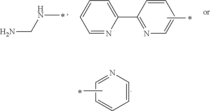
- a is a natural number of 1 to 20; and each R is independently
- the reactive monomer of Formula 1 may be represented by Formula 2 below:
- the reactive monomer of Formula 1 may be represented by Formula 3 below:
- the reactive monomer of Formula 1 may be represented by Formula 4 below:
- the reactive monomer of Formula 1 may include a mixture of reactive monomer A in which each R is independently
- any one or two of R may be
- a liquid crystal display includes a first substrate, a second substrate facing the first substrate, a liquid crystal layer disposed between the first substrate and the second substrate, a first liquid crystal alignment layer disposed between the liquid crystal layer and the first substrate, and a second liquid crystal alignment layer which is disposed between the liquid crystal layer and the second substrate, wherein at least one of the first liquid crystal alignment layer and the second liquid crystal alignment layer comprises a reactive monomer represented by Formula 1 below:
- each X is independently ⁇ —O— ⁇
- each N is independently
- a is a natural number of 1 to 20; and each R is independently
- b is a natural number of 1 to 20.
- the reactive monomer of Formula 1 may be represented by Formula 2 below:
- the reactive monomer of Formula 1 may be represented by Formula 3 below:
- the reactive monomer of Formula 1 may be represented by Formula 4 below:
- the reactive monomer of Formula 1 includes a mixture of reactive monomer A in which each R may be independently
- the reactive monomer of Formula 1 any one or two of R may be
- both the first liquid crystal alignment layer and the second liquid crystal alignment layer may include the reactive monomer of Formula 1.
- a method of manufacturing an LCD includes preparing a first substrate and a second substrate facing each other, injecting a liquid crystal composition into a space between the first substrate and the second substrate, irradiating UV light toward at least one of the first substrate and the second substrate in the absence of an electric field, and irradiating UV light toward at least one of the first substrate and the second substrate in the presence of the electric field, wherein the liquid crystal composition comprises a reactive monomer represented by Formula 1 below:
- each X is independently ⁇ —O— ⁇
- each N is independently
- a is a natural number from 1 to 20; and each R is independently
- b is a natural number of 1 to 20.
- the irradiating of the UV light in the absence of the electric field may polymerize the reactive monomer to form a first liquid crystal alignment layer on a surface of the first substrate which faces the second substrate and a second liquid crystal alignment layer on a surface of the second substrate which faces the first substrate.
- the injecting of the liquid crystal composition further includes forming a liquid crystal layer including first liquid crystal molecules aligned on a surface of the first liquid crystal alignment layer and second liquid crystal molecules aligned on a surface of the second liquid crystal alignment layer, and the irradiating of the UV light in the absence of the electric field aligns the first liquid crystal molecules and the second liquid crystal molecules in a direction perpendicular to the first substrate or the second substrate, wherein the first liquid crystal molecules and the second liquid crystal molecules have negative dielectric anisotropy.
- the method further includes removing the electric field after the irradiating of the UV light in the presence of the electric field, wherein the first liquid crystal molecules and the second liquid crystal molecules may be aligned at an angle relative to the first substrate or the second substrate after the irradiating of the UV light in the presence of the electric field.
- At least one of the first liquid crystal alignment layer and the second liquid crystal alignment layer may be formed as a single layer of the polymerized reactive monomer of Formula 1.
- the reactive monomer of Formula 1 any one or two of R may be
- the method of manufacturing an LCD may further comprise irradiating UV light again after the irradiating of the UV light in the presence of the electric field.
- FIG. 1 is a schematic exploded perspective view of an exemplary embodiment of a liquid crystal display (LCD);
- LCD liquid crystal display
- FIG. 2 is a schematic enlarged view of an area II of FIG. 1 ;
- FIG. 3 is a schematic cross-sectional view taken along line of FIG. 1 ;
- FIGS. 4 through 9 are schematic cross-sectional views illustrating an exemplary embodiment of a method of manufacturing an LCD.
- first, second, third, and so forth are used to describe diverse constituent elements, such constituent elements are not limited by the terms. The terms are used only to discriminate a constituent element from another constituent element. Accordingly, in the following description, a first constituent element may be a second constituent element.
- spatially relative terms such as “bottom,” “below,” “lower,” “under,” “above,” “upper,” “top” and the like, may be used herein for ease of description to describe the relationship of one element or feature to another element(s) or feature(s) as illustrated in the figures. It will be understood that the spatially relative terms are intended to encompass different orientations of the device in use or operation, in addition to the orientation depicted in the figures. For example, if the device in the figures is turned over, elements described as “below” or “beneath” relative to other elements or features would then be oriented “above” relative to the other elements or features. Thus, the exemplary term “below” can encompass both an orientation of above and below. The device may be otherwise oriented (rotated 90 degrees or at other orientations) and the spatially relative descriptors used herein interpreted accordingly.
- “About” or “approximately” as used herein is inclusive of the stated value and means within an acceptable range of deviation for the particular value as determined by one of ordinary skill in the art, considering the measurement in question and the error associated with measurement of the particular quantity (i.e., the limitations of the measurement system). For example, “about” can mean within one or more standard deviations, or within ⁇ 30%, 20%, 10%, 5% of the stated value.”
- Exemplary embodiments are described herein with reference to cross section illustrations that are schematic illustrations of idealized embodiments. As such, variations from the shapes of the illustrations as a result, for example, of manufacturing techniques and/or tolerances, are to be expected. Thus, embodiments described herein should not be construed as limited to the particular shapes of regions as illustrated herein but are to include deviations in shapes that result, for example, from manufacturing. For example, a region illustrated or described as flat may, typically, have rough and/or nonlinear features. Moreover, sharp angles that are illustrated may be rounded. Thus, the regions illustrated in the figures are schematic in nature and their shapes are not intended to illustrate the precise shape of a region and are not intended to limit the scope of the present claims.
- An alignment layer composition according to an embodiment of the present invention includes a reactive monomer represented by Formula 1 below:
- each X is independently ⁇ —O— ⁇
- each N is independently
- a is a natural number of 1 to 20; and each R is independently
- b is a natural number of 1 to 20.
- a first liquid crystal alignment layer and a second liquid crystal alignment layer may be formed on a surface of a pixel electrode and a surface of a common electrode which face each other in a liquid crystal display (LCD).
- the reactive monomer may be mixed with liquid crystals and introduced accordingly into the LCD. Therefore, a separate process of forming an alignment layer can be omitted.
- a liquid crystal alignment layer is formed by coating an alignment layer on a pixel electrode or on a common electrode, that is, on surfaces of the pixel electrode and the common electrode which face each other, and then drying the alignment layer.
- the alignment layer composition described herein is utilized, the separate process of forming an alignment layer is not necessary.
- a liquid crystal alignment layer can be formed by injecting a liquid crystal composition including the alignment layer composition and performing a subsequent process. That is, the liquid crystal alignment layer can be formed more easily.
- the reactive monomer of Formula 1 may include a mixture of reactive monomer A in which the R is
- the reactive monomer of Formula 1 includes two or more types of reactive monomers to form a liquid crystal alignment layer through the polymerization of the two or more types of reactive monomers.
- a liquid crystal alignment layer including a polymerization product of two or more types of monomers causes liquid crystal molecules located on the surface of the liquid crystal alignment layer to be aligned vertically and to pretilt.
- the reactive monomer of Formula 1 may be a single reactive monomer in which any one or two of R is
- the reactive monomer of Formula 1 can be represented by, for example, Formulas 2 through 4 below:
- FIG. 1 is a schematic exploded perspective view of an exemplary embodiment of an LCD 500 .
- FIG. 2 is a schematic enlarged view of area II of FIG. 1 .
- the exemplary LCD 500 includes a first substrate 100 , a second substrate 200 which is separated from the first substrate 100 and faces the first substrate 100 , and a liquid crystal layer 300 which is disposed between the first substrate 100 and the second substrate 200 .
- Each of the first and second substrates 100 and 200 includes a display area DA and a non-display area NDA.
- the display area DA is an area in which an image is displayed
- the non-display area NDA is an area in which no image is displayed.
- the display area DA is surrounded by the non-display area NDA.
- a common electrode 110 may be disposed between the first substrate 100 and the second substrate 200 and may be a patternless electrode without a slit pattern.
- a pixel electrode 291 may be disposed between the second substrate 200 and the common electrode 110 and may be a patterned electrode having a slit pattern.
- the liquid crystal layer 300 may be disposed between the common electrode 110 and the pixel electrode 291 .
- the liquid crystal layer 300 may include liquid crystal molecules LC having negative dielectric anisotropy.
- a first liquid crystal alignment layer AL 1 may be disposed between the common electrode 110 and the liquid crystal layer 300
- a second liquid crystal alignment layer AL 2 may be disposed between the pixel electrode 291 and the liquid crystal layer 300 .
- the second substrate 200 may be a thin-film transistor (TFT) substrate.
- TFT thin-film transistor
- a plurality of gate lines GL extending in a first direction and a plurality of data lines DL extending in a second direction perpendicular to the first direction may be formed in the display area DA of the second substrate 200 .
- the pixel electrode 291 may be disposed in each of pixels PX defined by the gate lines GL and the data lines DL.
- the pixel electrode 291 may include subpixel electrodes 291 - 1 and 291 - 2 separated from each other.
- each of the subpixel electrodes 291 - 1 and 291 - 2 may have a quadrilateral shape.
- Each of the subpixel electrodes 291 - 1 and 291 - 2 may be a patterned electrode having a slit pattern.
- the slit pattern may consist of a stem SC and slits DC disposed between branches BC extending from the stem SC.
- the stem SC may be shaped like a cross (+), and the branches BC may extend radially from the cross-shaped stem SC in a direction at an angle of approximately 45 degrees to the stem SC.
- a gate line GL may include gate electrodes 224 - 1 and 224 - 2 which protrude from the gate line GL in the second direction toward the pixel electrode 291 .
- a plurality of data lines DL may include source electrodes 273 - 1 and 273 - 2 and drain electrodes 275 - 1 and 275 - 2 .
- the source electrodes 273 - 1 and 273 - 2 may extend from the data lines DL in a “U” shape.
- the drain electrodes 275 - 1 and 275 - 2 may be separated from the source electrodes 273 - 1 and 273 - 2 .
- the pixel electrode 291 may receive a data voltage through a TFT, which is a switching device.
- the gate electrodes 224 - 1 and 224 - 2 which are control terminals of TFTs may be electrically connected to the gate line GL
- the source electrodes 273 - 1 and 273 - 2 which are input terminals of the TFTs may be electrically connected to the data lines DL via contact holes 285 - 1 , 285 - 2 , 285 - 3 , and 285 - 4
- the drain electrodes 275 - 1 and 275 - 2 which are output terminals of the TFTs may be electrically connected to the pixel electrode 291 .
- the pixel electrode 291 may generate an electric field together with the common electrode 110 , thereby controlling the alignment direction of the liquid crystal molecules LC of the liquid crystal layer 300 interposed therebetween.
- the pixel electrode 291 may control the alignment direction of first liquid crystal molecules LC 1 and the alignment direction of second liquid crystal molecules LC 2 by distorting the electric field.
- the TFT substrate may include a stack of a base substrate (not illustrated) which is made of glass or polymer, the gate electrodes 224 - 1 and 224 - 2 , a gate insulating layer (not illustrated), a semiconductor layer (not illustrated), an ohmic contact layer (not illustrated), the source electrodes 273 - 1 and 273 - 2 , the drain electrodes 275 - 1 and 275 - 2 , a passivation layer (not illustrated), and an organic layer (not illustrated), etc.
- a channel of a TFT may be formed of the semiconductor layer (not illustrated).
- the semiconductor layer (not illustrated) may overlap the gate electrodes 224 - 1 and 224 - 2 .
- the source electrodes 273 - 1 and 273 - 2 may be separated from the drain electrodes 275 - 1 and 275 - 2 with respect to the semiconductor layer (not illustrated), respectively.
- a storage electrode line SL may include a stem line 231 extending substantially parallel to the gate lines GL and a plurality of branch lines 235 extending from the stem line 231 .
- the storage electrode line SL can be omitted, and the shape and position of the storage electrode line SL can be changed variously.
- the non-display area NDA may be a light-blocking area surrounding the display area DA.
- a driving unit (not illustrated) which provides a gate driving signal, a data driving signal, etc. to each pixel PX of the display area DA may be disposed in the non-display area NDA of the second substrate 200 .
- the gate lines GL and the data lines DL may extend from the display area DA to the non-display area NDA so as to be electrically connected to the driving unit (not illustrated).
- the first substrate 100 may be a counter substrate of the second substrate 200 .
- the common electrode 110 may be disposed on the second substrate 200 .
- a color filter layer may be formed in an area corresponding to each pixel PX of the display area DA and include a red color filter (R), a green color filter (G) and a blue color filter (B).
- the color filter layer (not illustrated) may be included in any one of the first substrate 100 and the second substrate 200 .
- the first substrate 100 includes the color filter layer (not illustrated), it may have a structure in which a base substrate (not illustrated) made of glass or polymer, the color filter layer (not illustrated), and an overcoat layer (not illustrated) are stacked.
- the overcoat layer (not illustrated) may be a planarization layer which covers the color filter layer (not illustrated).
- the common electrode 110 may be disposed on the overcoat layer (not illustrated).
- the second substrate 200 may have a color filter-on-array (COA) structure in which color filters are formed on a transparent insulating substrate having TFTs.
- COA color filter-on-array
- the color filter layer (not illustrated) may be disposed between the passivation layer (not illustrated) which covers the source electrodes 273 - 1 and 273 - 2 and the drain electrodes 275 - 1 and 275 - 2 and the organic layer (not illustrated).
- a light-blocking pattern layer may be disposed at the boundary of each color filter R, G or B.
- the light-blocking pattern layer may be included in any one of the first substrate 100 and the second substrate 200 .
- the light-blocking pattern layer may be a black matrix.
- FIG. 3 is a schematic cross-sectional view taken along line of FIG. 1 .
- the exemplary LCD 500 will now be described in greater detail with reference to FIG. 3 .
- FIG. 3 schematically illustrates the alignment of liquid crystal molecules (LC 1 - 1 , LC 1 - 2 , LC 2 - 1 and LC 2 - 2 ) in an initial state in which the electric field is absent, i.e. no electric field has been applied to the LCD 500 .
- first liquid crystal molecules LC 1 - 1 and LC 1 - 2 may be aligned on a surface of the first liquid crystal alignment layer AL 1
- second liquid crystal molecules LC 2 - 1 and LC 2 - 2 may be aligned on a surface of the second liquid crystal alignment layer AL 2
- first liquid crystal molecules LC 1 - 1 and LC 1 - 2 and the second liquid crystal molecules LC 2 - 1 and LC 2 - 2 may be arranged at a certain pretilt angle on the surface of the first liquid crystal alignment layer AL 1 and the second liquid crystal alignment layer AL 2 , respectively.
- the (1-1) th liquid crystal molecules LC 1 - 1 and (1-2) th liquid crystal molecules LC 1 - 2 may form two or more domains having different alignment directions on the surface of the first liquid crystal alignment layer AL 1 .
- the (2-1) th liquid crystal molecules LC 2 - 1 and (2-2) th liquid crystal molecules LC 2 - 2 may form two or more domains having different alignment directions on the surface of the second liquid crystal alignment layer AL 2 .
- the alignment directions of the first liquid crystal molecules LC 1 - 1 and LC 1 - 2 in the domains formed by the first liquid crystal molecules LC 1 - 1 and LC 1 - 2 on the surface of the first liquid crystal alignment layer AL 1 may correspond to those of the second liquid crystal molecules LC 2 - 1 and LC 2 - 2 in the domains formed by the second liquid crystal molecules LC 2 - 1 and LC 2 - 2 on the surface of the second liquid crystal alignment layer AL 2 .
- first liquid crystal molecules LC 1 - 1 and LC 1 - 2 and the second liquid crystal molecules LC 2 - 1 and LC 2 - 2 on the surface of the first liquid crystal alignment layer AL 1 and the surface of the second liquid crystal layer AL 2 may have the same pretilt direction along the same straight line.
- the (1-1) th liquid crystal molecules LC 1 - 1 of the first alignment layer AL 1 may be aligned in a first tilt direction
- the (1-2) th liquid crystal molecules LC 1 - 2 of the first alignment layer AL 1 may be aligned in a second tilt direction.
- the (2-1) th liquid crystal molecules LC 2 - 1 of the second liquid crystal layer AL 2 which are located at positions vertically corresponding to the (1-1) th liquid crystal molecules LC 1 - 1 of the first liquid crystal alignment layer AL 1 may be aligned in the first tilt direction
- the (2-2) th liquid crystal molecules LC 2 - 2 which are located at positions vertically corresponding to the (1-2) th liquid crystal molecules LC 1 - 2 of the first liquid crystal alignment layer AL 1 may be aligned in the second tilt direction.
- the first tilt direction may be a direction at an angle of approximately ⁇ degrees with respect to a virtual straight line perpendicular to the first liquid crystal alignment layer AL 1 or the second liquid crystal alignment layer AL 2
- the second tilt direction may be a direction at an angle of approximately + ⁇ degrees with respect to the same virtual straight line.
- ⁇ is a positive real number.
- At least one of the first liquid crystal alignment layer AL 1 and the second liquid crystal alignment layer AL 2 may include the reactive monomer of Formula 1.
- both the first liquid crystal alignment layer AL 1 and the second liquid crystal alignment layer AL 2 may include the reactive monomer of Formula 1 below so as to cause the liquid crystal molecules LC 1 - 1 , LC 1 - 2 , LC 2 - 1 , and LC 2 - 2 to be aligned vertically and to pretilt.
- each X is independently ⁇ —O— ⁇
- each N is independently
- a is a natural number of 1 to 20; and each R is independently
- b is a natural number of 1 to 20.
- the reactive monomer may enable the liquid crystal molecules LC 1 - 1 , LC 1 - 2 , LC 2 - 1 , and LC 2 - 2 located on the surface of the first liquid crystal alignment layer AL 1 and the surface of the second liquid crystal alignment layer AL 2 to be aligned vertically and to have a certain pretilt angle as described above.
- the reactive monomer of Formula 1 may include a mixture of reactive monomer A in which each R is independently
- the reactive monomer A may polymerize on the first substrate 100 or the second substrate 200 to form the first and second liquid crystal alignment layers AL 1 and AL 2 , and the reactive monomer B may cause the liquid crystal molecules LC 1 - 1 , LC 1 - 2 , LC 2 - 1 , and LC 2 - 2 on the first liquid crystal alignment layer AL 1 or the second liquid crystal alignment layer AL 2 to be aligned vertically.
- the reactive monomer of Formula 1 may be a single compound in which any one or two of R is
- R functional groups selected from
- liquid crystal molecules LC 1 - 1 and LC 1 - 2 or LC 2 - 1 and LC 2 - 2 may cause the liquid crystal molecules LC 1 - 1 and LC 1 - 2 or LC 2 - 1 and LC 2 - 2 to be aligned vertically on the first liquid crystal alignment layer AL 1 or the second liquid crystal alignment layer AL 2 .
- the reactive monomer of Formula 1 may be any one of Formulas 2 through 4 below:
- At least one of the first liquid crystal alignment layer AL 1 and the second liquid crystal alignment layer AL 2 may further include a polymerization initiator to facilitate the polymerization of the reactive monomer. Since the polymerization initiator is widely known to those of ordinary skill in the art, a detailed description thereof is omitted.
- FIGS. 4 through 9 are schematic cross-sectional views illustrating an exemplary embodiment of a method of manufacturing the LCD 500 .
- a first substrate 100 is placed to face a second substrate 200 with a predetermined cell gap maintained therebetween.
- the second substrate 200 may be a TFT substrate
- the first substrate 100 may be a counter substrate of the second substrate 200 as well as a color filter substrate.
- a common electrode 110 may be placed under the first substrate 100 , that is, on a surface of the first substrate 100 which faces the second substrate 200 .
- the common electrode 110 may be made of a material including at least one of indium tin oxide, indium zinc oxide, indium oxide, zinc oxide, tin oxide, gallium oxide, titanium oxide, aluminum, silver, platinum, chrome, molybdenum, tantalum, niobium, zinc, magnesium, any alloy thereof, and a stack thereof.
- the common electrode 110 may be a patternless electrode without a slit pattern.
- a pixel electrode 291 may be placed on the second substrate 200 and may be made of a material including at least one of indium tin oxide, indium zinc oxide, indium oxide, zinc oxide, tin oxide, gallium oxide, titanium oxide, aluminum, silver, platinum, chrome, molybdenum, tantalum, niobium, zinc, magnesium, any alloy thereof, and a stack thereof.
- the pixel electrode 291 may be a patterned electrode having a slit pattern, and part of the second substrate 200 may be exposed through the slit pattern of the pixel electrode 291 .
- a liquid crystal layer 300 is disposed between the first substrate 100 and the second substrate 200 which face each other. That is, liquid crystals are injected into a space between the first substrate 100 and the second substrate 200 .
- the liquid crystal layer 300 may be formed by injecting or dropping a liquid crystal composition that contains liquid crystal molecules LC 1 , LC 2 into the space between the first substrate 100 and the second substrate 200 .
- the liquid crystal layer 300 may include the above-described alignment layer composition comprising the reactive monomer of Formula 1 in addition to the liquid crystal composition.
- the liquid crystal composition may further contain a polymerization initiator to facilitate the polymerization reaction of the reactive monomer contained in a first liquid crystal alignment layer AL 1 and a second liquid crystal alignment layer AL 2 .
- ultraviolet (UV) light is irradiated toward at least any one of the first substrate 100 and the second substrate 200 in the absence of an electric field.
- a polymerization reaction of the reactive monomers RM included in the liquid crystal layer 300 may be initiated on a surface of the common electrode 110 which faces the second substrate 200 , and on the first substrate 100 and the pixel electrode 291 , thereby forming the first liquid crystal alignment layer AL 1 and the second liquid crystal alignment layer AL 2 as illustrated in FIG. 7 .
- the liquid crystal layer 300 may also include the above-described polymerization initiator to facilitate the polymerization reaction.
- the irradiating of the UV light in the absence of the electric field may initiate polymerization of the reactive monomers RM to form the first liquid crystal alignment layer AL 1 and the second liquid crystal alignment layer AL 2 .
- the polymers of the reactive monomers RM may be shaped as protrusions.
- the irradiating of the UV light in the absence of the electric field may cause the liquid crystal composition on the first liquid crystal alignment layer AL 1 and the second liquid crystal alignment layer AL 2 to be aligned vertically.
- each liquid crystal molecule LC may have negative dielectric anisotropy.
- the liquid crystal molecules LC may be aligned substantially perpendicularly to the first substrate 100 and the second substrate 200 by the irradiating of the UV light to the LCD 500 in the absence of the electric field.
- the liquid crystal molecules LC when aligned substantially perpendicularly to the first substrate 100 and the second substrate 200 , they may be aligned at an angle of, e.g., about 87.5 to less than about 90 degrees to the first substrate 100 and the second substrate 200 .
- the irradiating of the UV light in the absence of the electric field may cause some of the reactive monomers RM existing in the liquid crystal layer 300 to form the first liquid crystal alignment layer AL 1 and the second liquid crystal alignment layer AL 2 . Accordingly, the reactive monomer content of the liquid crystal layer 300 may be reduced. It can be understood that the reduced amount of the reactive monomers RM corresponds to the amount of reactive monomer used to form the first liquid crystal alignment layer AL 1 or the second liquid crystal alignment layer AL 2 .
- the liquid crystal molecules LC 1 - 1 , LC 1 - 2 , LC 2 - 1 , and LC 2 - 2 may tilt in a direction perpendicular to the electric field formed between the common electrode 110 and the pixel electrode 291 . That is, the (1-1) th liquid crystal molecules LC 1 - 1 and the (2-1) th liquid crystal molecules LC 2 - 1 may be aligned in a first tilt direction, and the (1-2) th liquid crystal molecules LC 1 - 2 and (2-2) th liquid crystal molecules LC 2 - 2 may be aligned in a second tilt direction.
- UV light is irradiated to the LCD 500 in the presence of the electric field. Accordingly, photopolymerization of the reactive monomers RM contained in the first liquid crystal alignment layer AL 1 and the second liquid crystal alignment layer AL 2 may be initiated, thus causing the (1-1) th liquid crystal molecules LC 1 - 1 and the (2-1) th liquid crystal molecules LC 2 - 1 to be aligned in the first tilt direction and the (1-2) th liquid crystal molecules LC 1 - 2 and the (2-2) th liquid crystal molecules LC 2 - 2 to be aligned in the second tilt direction.
- the irradiating of the UV light in the presence of the electric field may cause the reactive monomer content of the liquid crystal layer 300 to be reduced further.
- the first liquid crystal alignment layer AL 1 or the second liquid crystal alignment layer AL 2 may fix or stabilize the alignment direction of first liquid crystal molecules LC 1 - 1 , LC 1 - 2 and the alignment direction of second liquid crystal molecules LC 2 - 1 , LC 2 - 2 . Therefore, the first liquid crystal molecules LC 1 - 1 , LC 1 - 2 and the second liquid crystal molecules LC 2 - 1 , LC 2 - 2 aligned on the surface of the first liquid crystal alignment layer AL 1 or the second liquid crystal alignment layer AL 2 , may remain tilted even after the electric field applied to the LCD 500 is removed.
- the remaining reactive monomers RM may be removed by irradiating fluorescent UV light to the LCD 500 . That is, the reactive monomers RM remaining in the liquid crystal layer 300 after failing to react in the irradiating of the UV light in the presence of the electric field can be removed.
- an alignment layer composition can increase the vertical alignment of liquid crystals and cause the liquid crystals to pretilt easily.
- a liquid crystal layer in an LCD including the alignment layer composition, can be easily aligned vertically and pretilted.
Landscapes
- Chemical & Material Sciences (AREA)
- Physics & Mathematics (AREA)
- Organic Chemistry (AREA)
- Nonlinear Science (AREA)
- Crystallography & Structural Chemistry (AREA)
- Optics & Photonics (AREA)
- Mathematical Physics (AREA)
- General Physics & Mathematics (AREA)
- Spectroscopy & Molecular Physics (AREA)
- Engineering & Computer Science (AREA)
- Materials Engineering (AREA)
- Health & Medical Sciences (AREA)
- Chemical Kinetics & Catalysis (AREA)
- Medicinal Chemistry (AREA)
- Polymers & Plastics (AREA)
- Liquid Crystal (AREA)
Abstract

Description

where in Formula 1 n is 0 or 1; C is

each X is independently ★—O—★,

or a bond; each N is independently

wherein a is a natural number of 1 to 20; and each R is independently

wherein b is a natural number of 1 to 20


and reactive monomer B in which each R is independently


and the other one or two of R may be


wherein in Formula 1 n is 0 or 1; C is

each X is independently ★—O—★,

or a bond; each N is independently

wherein a is a natural number of 1 to 20; and each R is independently

wherein b is a natural number of 1 to 20.


and reactive monomer B in which each R is independently


and the other one or two of R is


wherein in Formula 1 n is 0 or 1; C is

each X is independently ★—O—★,

or a bond; each N is independently

wherein a is a natural number from 1 to 20; and each R is independently

wherein b is a natural number of 1 to 20.

and the other one or two of R may be

where in Formula 1 n is 0 or 1; C is

each X is independently ★—O—★,

or a bond; each N is independently

wherein a is a natural number of 1 to 20; and each R is independently

wherein b is a natural number of 1 to 20.

and reactive monomer B in which the R is

That is, the reactive monomer of Formula 1 includes two or more types of reactive monomers to form a liquid crystal alignment layer through the polymerization of the two or more types of reactive monomers. A liquid crystal alignment layer including a polymerization product of two or more types of monomers causes liquid crystal molecules located on the surface of the liquid crystal alignment layer to be aligned vertically and to pretilt.

and the other one or two of R is


In Formula 1 n is 0 or 1; C is

each X is independently ★—O—★,

or a bond; each N is independently

where a is a natural number of 1 to 20;
and each R is independently

where b is a natural number of 1 to 20.

and reactive monomer B in which each R is independently


and the other one or two of R is

The R functional groups selected from

may help in the polymerization reaction for forming the first liquid crystal alignment layer AL1 or the second liquid crystal alignment layer AL2. The functional group R selected from

may cause the liquid crystal molecules LC1-1 and LC1-2 or LC2-1 and LC2-2 to be aligned vertically on the first liquid crystal alignment layer AL1 or the second liquid crystal alignment layer AL2.


Claims (15)


Applications Claiming Priority (2)
| Application Number | Priority Date | Filing Date | Title |
|---|---|---|---|
| KR10-2015-0130017 | 2015-09-15 | ||
| KR1020150130017A KR102431192B1 (en) | 2015-09-15 | 2015-09-15 | Composition for alignment layer, liquid crystal display comprising the composition and method for manufacturing the liquid crystal display |
Publications (2)
| Publication Number | Publication Date |
|---|---|
| US20170075173A1 US20170075173A1 (en) | 2017-03-16 |
| US10088709B2 true US10088709B2 (en) | 2018-10-02 |
Family
ID=58236814
Family Applications (1)
| Application Number | Title | Priority Date | Filing Date |
|---|---|---|---|
| US15/072,995 Active 2036-12-10 US10088709B2 (en) | 2015-09-15 | 2016-03-17 | Alignment layer composition, liquid crystal display including the same, and method of manufacturing the liquid crystal display |
Country Status (2)
| Country | Link |
|---|---|
| US (1) | US10088709B2 (en) |
| KR (1) | KR102431192B1 (en) |
Families Citing this family (5)
| Publication number | Priority date | Publication date | Assignee | Title |
|---|---|---|---|---|
| US10190050B2 (en) | 2016-01-21 | 2019-01-29 | Samsung Display Co., Ltd. | Liquid crystal composition, liquid crystal display device including the same, and method of manufacturing liquid crystal display device |
| US10041001B2 (en) | 2016-01-21 | 2018-08-07 | Samsung Display Co., Ltd. | Liquid crystal composition, liquid crystal display device including the same, and method of manufacturing liquid crystal display device |
| KR20180019794A (en) * | 2016-08-16 | 2018-02-27 | 삼성디스플레이 주식회사 | Liquid crystal display apparatus and method of manufacturing the same |
| CN107505756A (en) * | 2017-09-27 | 2017-12-22 | 深圳市华星光电半导体显示技术有限公司 | A kind of liquid crystal display panel and its manufacture method |
| KR102431838B1 (en) * | 2020-05-29 | 2022-08-12 | 한국과학기술연구원 | Acrylate compound, polyacrylate, and polyacrylate film containing the polyacrylate |
Citations (2)
| Publication number | Priority date | Publication date | Assignee | Title |
|---|---|---|---|---|
| US20130287970A1 (en) * | 2012-04-28 | 2013-10-31 | Shenzhen China Star Optoelectronics Technology Co., Ltd | Liquid Crystal Medium Composition and Liquid Crystal Display Using Same |
| KR20170019544A (en) | 2015-08-11 | 2017-02-22 | 삼성디스플레이 주식회사 | Curved liquid crystal display and method for manufacturing the same |
-
2015
- 2015-09-15 KR KR1020150130017A patent/KR102431192B1/en active Active
-
2016
- 2016-03-17 US US15/072,995 patent/US10088709B2/en active Active
Patent Citations (2)
| Publication number | Priority date | Publication date | Assignee | Title |
|---|---|---|---|---|
| US20130287970A1 (en) * | 2012-04-28 | 2013-10-31 | Shenzhen China Star Optoelectronics Technology Co., Ltd | Liquid Crystal Medium Composition and Liquid Crystal Display Using Same |
| KR20170019544A (en) | 2015-08-11 | 2017-02-22 | 삼성디스플레이 주식회사 | Curved liquid crystal display and method for manufacturing the same |
Also Published As
| Publication number | Publication date |
|---|---|
| KR20170032907A (en) | 2017-03-24 |
| US20170075173A1 (en) | 2017-03-16 |
| KR102431192B1 (en) | 2022-08-10 |
Similar Documents
| Publication | Publication Date | Title |
|---|---|---|
| US9568785B2 (en) | Liquid crystal display | |
| US8153208B2 (en) | Liquid crystal display, a method for manufacturing a liquid crystal display and a liquid crystal composition | |
| US20170075173A1 (en) | Alignment layer composition, liquid crystal display including the same, and method of manufacturing the liquid crystal display | |
| US10018875B2 (en) | Curved liquid crystal display and method of manufacturing the same | |
| US9989809B2 (en) | Curved liquid crystal display and method of manufacturing the same | |
| US10234728B2 (en) | Liquid crystal display device and method of manufacturing the same | |
| US9678387B2 (en) | Liquid crystal display and method of manufacturing the same | |
| US20130287970A1 (en) | Liquid Crystal Medium Composition and Liquid Crystal Display Using Same | |
| US9823514B2 (en) | Liquid crystal display and method for manufacturing the same | |
| US10558087B2 (en) | Liquid crystal display and manufacturing method thereof | |
| US11391992B2 (en) | Liquid crystal display and manufacturing method thereof | |
| US9207495B2 (en) | Liquid crystal display device | |
| US20160209707A1 (en) | Liquid crystal display and manufacturing method of making the liquid crystal display | |
| US10394084B2 (en) | Liquid crystal display and method of manufacturing the same | |
| US9904113B2 (en) | Alignment composition, liquid crystal display panel and method of manufacturing same | |
| US10503020B2 (en) | Liquid crystal display and method of manufacturing the same | |
| US9977288B2 (en) | Liquid crystal display | |
| US9454040B2 (en) | Liquid crystal display | |
| US20170031213A1 (en) | Liquid crystal display | |
| US20170015904A1 (en) | Liquid crystal composition and liquid crystal display including the same | |
| US20160240161A1 (en) | Liquid crystal display | |
| US10503017B2 (en) | Liquid crystal display and manufacturing method thereof | |
| US20150240032A1 (en) | Photoalignment agent and liquid crystal display device including the same | |
| US9671648B2 (en) | Liquid crystal display and method of manufacturing the same | |
| US10444571B2 (en) | Liquid crystal display and method of manufacturing the same |
Legal Events
| Date | Code | Title | Description |
|---|---|---|---|
| AS | Assignment |
Owner name: SAMSUNG DISPLAY CO., LTD., KOREA, REPUBLIC OF Free format text: ASSIGNMENT OF ASSIGNORS INTEREST;ASSIGNOR:HO, LIM;REEL/FRAME:038256/0851 Effective date: 20160119 |
|
| STCF | Information on status: patent grant |
Free format text: PATENTED CASE |
|
| MAFP | Maintenance fee payment |
Free format text: PAYMENT OF MAINTENANCE FEE, 4TH YEAR, LARGE ENTITY (ORIGINAL EVENT CODE: M1551); ENTITY STATUS OF PATENT OWNER: LARGE ENTITY Year of fee payment: 4 |
|
| MAFP | Maintenance fee payment |
Free format text: PAYMENT OF MAINTENANCE FEE, 8TH YEAR, LARGE ENTITY (ORIGINAL EVENT CODE: M1552); ENTITY STATUS OF PATENT OWNER: LARGE ENTITY Year of fee payment: 8 |