US10190050B2 - Liquid crystal composition, liquid crystal display device including the same, and method of manufacturing liquid crystal display device - Google Patents
Liquid crystal composition, liquid crystal display device including the same, and method of manufacturing liquid crystal display device Download PDFInfo
- Publication number
- US10190050B2 US10190050B2 US15/408,958 US201715408958A US10190050B2 US 10190050 B2 US10190050 B2 US 10190050B2 US 201715408958 A US201715408958 A US 201715408958A US 10190050 B2 US10190050 B2 US 10190050B2
- Authority
- US
- United States
- Prior art keywords
- liquid crystal
- substituted
- unsubstituted
- formula
- unsubstituted substituted
- Prior art date
- Legal status (The legal status is an assumption and is not a legal conclusion. Google has not performed a legal analysis and makes no representation as to the accuracy of the status listed.)
- Active
Links
- 0 C.C.C.C.C.CCCC*C[Y] Chemical compound C.C.C.C.C.CCCC*C[Y] 0.000 description 314
- BASRGRNFKMTWPH-UHFFFAOYSA-N C=C(C)C(=O)OCC(CCOC1=CC=C(C2=CC=C(OCCCCCCCCOC(=O)C3=CNC=N3)C=C2)C=C1)COC(=O)C(=C)C.C=C(C)C(=O)OCCC(CCOC(=O)C(=C)C)C1=CC=C(C2=C(CC)C=C(OCCCCCCC3=CC=C(CCOCCCCCCOC4=CC=NC=C4)C=C3)C=C2)C=C1.C=C(C)C(=O)OCCOC1=CC=C(C2=CC=C(OCCCOC3=CN=C(C4=NC=CC=C4)C=C3)C=C2)C=C1.C=CC(=O)OCCOC1=CC=C(C2=CC=C(OCCCCOP3(OCO)=NP(OCO)(OCO)=NP(OCO)(OCO)=N3)C=C2)C=C1.C=CC(=O)OCCOC1=CC=C(C2=CC=C(OCCCOC3C4=C(N=CC=C4)C4=C3C=CC=N4)C=C2)C=C1 Chemical compound C=C(C)C(=O)OCC(CCOC1=CC=C(C2=CC=C(OCCCCCCCCOC(=O)C3=CNC=N3)C=C2)C=C1)COC(=O)C(=C)C.C=C(C)C(=O)OCCC(CCOC(=O)C(=C)C)C1=CC=C(C2=C(CC)C=C(OCCCCCCC3=CC=C(CCOCCCCCCOC4=CC=NC=C4)C=C3)C=C2)C=C1.C=C(C)C(=O)OCCOC1=CC=C(C2=CC=C(OCCCOC3=CN=C(C4=NC=CC=C4)C=C3)C=C2)C=C1.C=CC(=O)OCCOC1=CC=C(C2=CC=C(OCCCCOP3(OCO)=NP(OCO)(OCO)=NP(OCO)(OCO)=N3)C=C2)C=C1.C=CC(=O)OCCOC1=CC=C(C2=CC=C(OCCCOC3C4=C(N=CC=C4)C4=C3C=CC=N4)C=C2)C=C1 BASRGRNFKMTWPH-UHFFFAOYSA-N 0.000 description 7
- IFEOUTBDBSMJMJ-UHFFFAOYSA-N C=C(C)C(=O)OCCC(CCOC(=O)C(=C)C)C1=CC=C(C2=C(CC)C=C(OCCCCCCC3=CC=C(CCCOC(=O)C4=CNC=N4)C=C3)C=C2)C=C1.C=C(C)C(=O)OCCC(CCOC(=O)C(=C)C)C1=CC=C(C2=C(CC)C=C(OCCCCCCC3=CC=C(CCOCCCCCCOC(=O)C4=CNC=N4)C=C3)C=C2)C=C1.C=C(C)C(=O)OCCC(CCOC(=O)C(=C)C)C1=CC=C(C2=C(CC)C=C(OCCCCCCC3=CC=C(CCOCCCCCCOC4=CC=C(C5=CC=CC=N5)N=C4)C=C3)C=C2)C=C1.C=C(C)C(=O)OCCCOC1=CC=C(C2=CC=C(CCCCC3=CC=C(OCCCCCOC4=CC=NC=C4)C=C3)C=C2CC)C=C1.C=C(C)C(=O)OCCCOC1=CC=C(C2=CC=C(CCCCC3=CC=NC=C3)C=C2CC)C=C1 Chemical compound C=C(C)C(=O)OCCC(CCOC(=O)C(=C)C)C1=CC=C(C2=C(CC)C=C(OCCCCCCC3=CC=C(CCCOC(=O)C4=CNC=N4)C=C3)C=C2)C=C1.C=C(C)C(=O)OCCC(CCOC(=O)C(=C)C)C1=CC=C(C2=C(CC)C=C(OCCCCCCC3=CC=C(CCOCCCCCCOC(=O)C4=CNC=N4)C=C3)C=C2)C=C1.C=C(C)C(=O)OCCC(CCOC(=O)C(=C)C)C1=CC=C(C2=C(CC)C=C(OCCCCCCC3=CC=C(CCOCCCCCCOC4=CC=C(C5=CC=CC=N5)N=C4)C=C3)C=C2)C=C1.C=C(C)C(=O)OCCCOC1=CC=C(C2=CC=C(CCCCC3=CC=C(OCCCCCOC4=CC=NC=C4)C=C3)C=C2CC)C=C1.C=C(C)C(=O)OCCCOC1=CC=C(C2=CC=C(CCCCC3=CC=NC=C3)C=C2CC)C=C1 IFEOUTBDBSMJMJ-UHFFFAOYSA-N 0.000 description 5
- FSLUDSQPXCBCIR-UHFFFAOYSA-N C=C(C)C(=O)OC1=CC=C(C2=CC(F)=C(OCCCCCCCCCCCOCC3CO3)C(F)=C2)C=C1.C=C(C)C(=O)OCCCCCCCCCOC1=CC(F)=C(C2=CC=C(OCOCC3CC(=O)OC(=O)C3)C=C2)C(F)=C1 Chemical compound C=C(C)C(=O)OC1=CC=C(C2=CC(F)=C(OCCCCCCCCCCCOCC3CO3)C(F)=C2)C=C1.C=C(C)C(=O)OCCCCCCCCCOC1=CC(F)=C(C2=CC=C(OCOCC3CC(=O)OC(=O)C3)C=C2)C(F)=C1 FSLUDSQPXCBCIR-UHFFFAOYSA-N 0.000 description 4
- UHAQCJCAXURMBT-UHFFFAOYSA-N C=C(C)C(=O)OC1=CC=C(C2=CC(F)=C(OCCCCCCCCCCCOCC3COC(=O)OC3)C(F)=C2)C=C1.C=C(C)C(=O)OCC(CCOC1=CC=C(C2=CC=C(OCCCCCCCOC3=CC=C(C4=CC=CC=N4)N=C3)C=C2)C=C1)COC(=O)C(=C)C.C=C(C)C(=O)OCC1=C(C2=CC=C(OCCC(COC(=O)C(=C)C)COC(=O)C(=C)C)C=C2)C=CC(OCCCCCCCOC2=CC=C(C3=CC=CC=N3)N=C2)=C1.C=C(C)C(=O)OCCCCOC1=CC=C(C2=C(CCOC(=O)C(=C)C)C=C(OCCCCCCCCOC(=O)C3=CNC=N3)C=C2)C=C1.C=C(C)C(=O)OCCCOC1=CC=C(C2=CC=C(CCCCC3=CC=C(OCCCCCOC4=CC=NC=C4)C=C3)C=C2COC(=O)C(=C)C)C=C1 Chemical compound C=C(C)C(=O)OC1=CC=C(C2=CC(F)=C(OCCCCCCCCCCCOCC3COC(=O)OC3)C(F)=C2)C=C1.C=C(C)C(=O)OCC(CCOC1=CC=C(C2=CC=C(OCCCCCCCOC3=CC=C(C4=CC=CC=N4)N=C3)C=C2)C=C1)COC(=O)C(=C)C.C=C(C)C(=O)OCC1=C(C2=CC=C(OCCC(COC(=O)C(=C)C)COC(=O)C(=C)C)C=C2)C=CC(OCCCCCCCOC2=CC=C(C3=CC=CC=N3)N=C2)=C1.C=C(C)C(=O)OCCCCOC1=CC=C(C2=C(CCOC(=O)C(=C)C)C=C(OCCCCCCCCOC(=O)C3=CNC=N3)C=C2)C=C1.C=C(C)C(=O)OCCCOC1=CC=C(C2=CC=C(CCCCC3=CC=C(OCCCCCOC4=CC=NC=C4)C=C3)C=C2COC(=O)C(=C)C)C=C1 UHAQCJCAXURMBT-UHFFFAOYSA-N 0.000 description 4
- ZMUALABBCHHQDY-UHFFFAOYSA-N CCCCCCCCOC1=CC=C(C2=CC=C(OCCCCNP3(NCN)=NP(NCN)(NCN)=NP(NCN)(NCN)=N3)C=C2)C=C1.CCCCCCCCOC1=CC=C(C2=CC=C(OCCCCOP3(OCO)=NP(OCO)(OCO)=NP(OCO)(OCO)=N3)C=C2)C=C1.CCCCCCCOC1=CC=C(C2=CC=C(OC(=O)C3=CNC=N3)C=C2)C=C1.CCCCCCCOC1=CC=C(C2=CC=C(OCCCOC(=O)C3=CC=NC=C3)C=C2)C=C1.CCCCCCCOC1=CC=C(C2=CC=C(OCCCOC3=CN=C(C4=NC=CC=C4)C=C3)C=C2)C=C1.CCCCCCCOC1=CC=C(C2=CC=C(OCCCOC3C4=C(N=CC=C4)C4=C3C=CC=N4)C=C2)C=C1 Chemical compound CCCCCCCCOC1=CC=C(C2=CC=C(OCCCCNP3(NCN)=NP(NCN)(NCN)=NP(NCN)(NCN)=N3)C=C2)C=C1.CCCCCCCCOC1=CC=C(C2=CC=C(OCCCCOP3(OCO)=NP(OCO)(OCO)=NP(OCO)(OCO)=N3)C=C2)C=C1.CCCCCCCOC1=CC=C(C2=CC=C(OC(=O)C3=CNC=N3)C=C2)C=C1.CCCCCCCOC1=CC=C(C2=CC=C(OCCCOC(=O)C3=CC=NC=C3)C=C2)C=C1.CCCCCCCOC1=CC=C(C2=CC=C(OCCCOC3=CN=C(C4=NC=CC=C4)C=C3)C=C2)C=C1.CCCCCCCOC1=CC=C(C2=CC=C(OCCCOC3C4=C(N=CC=C4)C4=C3C=CC=N4)C=C2)C=C1 ZMUALABBCHHQDY-UHFFFAOYSA-N 0.000 description 4
- KRJHLXRHUMTMKT-UHFFFAOYSA-N C=C(C)C(=O)OCCC1=CC(C2=CC=C(OC3CCOC3)C(CCOC(=O)C(=C)C)=C2)=CC=C1OCCCCCCCCCC.C=C(C)C(=O)OCCC1=CC(C2=CC=C(OCCN3CCOC3)C(CCOC(=O)C(=C)C)=C2)=CC=C1OCCCCCCCCCC.C=C(C)C(=O)OCCCC1=CC(C2=C(F)C=C(OCCCCCCCCCC)C=C2)=CC=C1OCOCC1CCNCC1 Chemical compound C=C(C)C(=O)OCCC1=CC(C2=CC=C(OC3CCOC3)C(CCOC(=O)C(=C)C)=C2)=CC=C1OCCCCCCCCCC.C=C(C)C(=O)OCCC1=CC(C2=CC=C(OCCN3CCOC3)C(CCOC(=O)C(=C)C)=C2)=CC=C1OCCCCCCCCCC.C=C(C)C(=O)OCCCC1=CC(C2=C(F)C=C(OCCCCCCCCCC)C=C2)=CC=C1OCOCC1CCNCC1 KRJHLXRHUMTMKT-UHFFFAOYSA-N 0.000 description 3
- WZBOJJLSENNEBO-UHFFFAOYSA-N C=C(C)C(=O)OCCCC1=C(OCC2=CON=C2)C=CC(C2=C(F)C=C(OCCCCCCCCCC)C=C2)=C1.C=C(C)C(=O)OCCCC1=CC(C2=C(CC)C=CC=C2)=CC(CCCOC(=O)C(=C)C)=C1OCCCCCC1=CC=C(OCCCOCC2CCOC2)C=C1.C=C(C)C(=O)OCCCC1=CC(C2=C(CC)C=CC=C2)=CC(CCCOC(=O)C(=C)C)=C1OCCCCCC1=CC=C(OCCCOCN2C=COC2)C=C1 Chemical compound C=C(C)C(=O)OCCCC1=C(OCC2=CON=C2)C=CC(C2=C(F)C=C(OCCCCCCCCCC)C=C2)=C1.C=C(C)C(=O)OCCCC1=CC(C2=C(CC)C=CC=C2)=CC(CCCOC(=O)C(=C)C)=C1OCCCCCC1=CC=C(OCCCOCC2CCOC2)C=C1.C=C(C)C(=O)OCCCC1=CC(C2=C(CC)C=CC=C2)=CC(CCCOC(=O)C(=C)C)=C1OCCCCCC1=CC=C(OCCCOCN2C=COC2)C=C1 WZBOJJLSENNEBO-UHFFFAOYSA-N 0.000 description 3
- CNCKAEFDHLRTLU-UHFFFAOYSA-N C=C(C)C(=O)OCCCC1=CC(C2=C(F)C=C(OCCCCCCCCCC)C=C2)=CC(CCCOC(=O)C(=C)C)=C1OCOCC1C=COC=C1.C=C(C)C(=O)OCCCC1=CC(C2=C(F)C=C(OCCCCCCCCCC)C=C2)=CC(CCCOC(=O)C(=C)C)=C1OCOCC1CC(=O)OC(=O)C1.C=C(C)C(=O)OCCCC1=CC(C2=C(F)C=C(OCCCCCCCCCC)C=C2)=CC(CCCOC(=O)C(=C)C)=C1OCOCC1CCOCC1 Chemical compound C=C(C)C(=O)OCCCC1=CC(C2=C(F)C=C(OCCCCCCCCCC)C=C2)=CC(CCCOC(=O)C(=C)C)=C1OCOCC1C=COC=C1.C=C(C)C(=O)OCCCC1=CC(C2=C(F)C=C(OCCCCCCCCCC)C=C2)=CC(CCCOC(=O)C(=C)C)=C1OCOCC1CC(=O)OC(=O)C1.C=C(C)C(=O)OCCCC1=CC(C2=C(F)C=C(OCCCCCCCCCC)C=C2)=CC(CCCOC(=O)C(=C)C)=C1OCOCC1CCOCC1 CNCKAEFDHLRTLU-UHFFFAOYSA-N 0.000 description 3
- CWFFXTNDFFAGKZ-UHFFFAOYSA-N C.C=C1OCC(C)(CC)CO1.C=C1OCC(C)(CC)O1.C=C1OCC(CC)CO1.C=C1OCC(CC)O1.CC1=COC=C1.CC1CCOC1.CCC1(C)CCOC(=O)C1.CCC1(C)CCOC1.CCC1(CC)COC1.CCC1=CCC=C1.CCC1=CCN=C1.CCC1C=COC=C1.CCC1CC(=O)CC1=O.CCC1CC(=O)OC(=O)C1.CCC1CC1.CCC1CCC(=O)C1.CCC1CCCC1.CCC1CCOC(=O)C1.CCC1CCOCC1.CCC1COC1.CCCN1CCOC1.CCN1C=COC1 Chemical compound C.C=C1OCC(C)(CC)CO1.C=C1OCC(C)(CC)O1.C=C1OCC(CC)CO1.C=C1OCC(CC)O1.CC1=COC=C1.CC1CCOC1.CCC1(C)CCOC(=O)C1.CCC1(C)CCOC1.CCC1(CC)COC1.CCC1=CCC=C1.CCC1=CCN=C1.CCC1C=COC=C1.CCC1CC(=O)CC1=O.CCC1CC(=O)OC(=O)C1.CCC1CC1.CCC1CCC(=O)C1.CCC1CCCC1.CCC1CCOC(=O)C1.CCC1CCOCC1.CCC1COC1.CCCN1CCOC1.CCN1C=COC1 CWFFXTNDFFAGKZ-UHFFFAOYSA-N 0.000 description 2
- VRINOMVJEGADEG-UHFFFAOYSA-N C1=CC2=C(N=C1)C1=C(/C=C\C=N/1)C2.C1=CN=C(C2=NC=CC=C2)C=C1.C1=CNC=N1.C=C(C)NC1=NC(NC(C)=O)=NC(C)=N1.C=C(N)NC1=NC(NC(N)=O)=NC(C)=N1.CC.CC.CC.CC1=NC(OC(C)O)=NC(OC(O)O)=N1.CC1=NC(OCCO)=NC(OCCO)=N1.CCCNC1=NC(NCCN)=NC(C)=N1.CCOC1=NC(OCO)=NC(C)=N1 Chemical compound C1=CC2=C(N=C1)C1=C(/C=C\C=N/1)C2.C1=CN=C(C2=NC=CC=C2)C=C1.C1=CNC=N1.C=C(C)NC1=NC(NC(C)=O)=NC(C)=N1.C=C(N)NC1=NC(NC(N)=O)=NC(C)=N1.CC.CC.CC.CC1=NC(OC(C)O)=NC(OC(O)O)=N1.CC1=NC(OCCO)=NC(OCCO)=N1.CCCNC1=NC(NCCN)=NC(C)=N1.CCOC1=NC(OCO)=NC(C)=N1 VRINOMVJEGADEG-UHFFFAOYSA-N 0.000 description 2
- CXCMHPVYXUPOIG-UHFFFAOYSA-N C1=CC=NC=C1.C=C(NC)NC1=NC(NC(=O)NC)=NC(CC)=N1.CC.CC.CC1=CN=C(C)N1C.CC1=NC(NCCN)=NC(NCCN)=N1.CC1CO1.CCC1=CC=NN=C1.CCC1CCNCC1.CCNC1=NC(NCN)=NC(C)=N1.CCNP1(NCN)=NP(NC)(NCN)=NP(NCN)(NCN)=N1.CCOP1(OCO)=NP(OC)(OCO)=NP(OCO)(OCO)=N1.CN1C=CN=C1.CN1C=CN=C1.CN1CNCNC1 Chemical compound C1=CC=NC=C1.C=C(NC)NC1=NC(NC(=O)NC)=NC(CC)=N1.CC.CC.CC1=CN=C(C)N1C.CC1=NC(NCCN)=NC(NCCN)=N1.CC1CO1.CCC1=CC=NN=C1.CCC1CCNCC1.CCNC1=NC(NCN)=NC(C)=N1.CCNP1(NCN)=NP(NC)(NCN)=NP(NCN)(NCN)=N1.CCOP1(OCO)=NP(OC)(OCO)=NP(OCO)(OCO)=N1.CN1C=CN=C1.CN1C=CN=C1.CN1CNCNC1 CXCMHPVYXUPOIG-UHFFFAOYSA-N 0.000 description 2
- QVCDTISFNRYTLV-UHFFFAOYSA-N C=C(C)C(=O)OC1=CC=C(C2=CC(F)=C(OCCCCCCCCCCCOCC3CO3)C(F)=C2)C=C1.C=C(C)C(=O)OC1=CC=C(C2=CC(F)=C(OCCCCCCCCCCCOCC3COC(=O)OC3)C(F)=C2)C=C1.C=C(C)C(=O)OCCCCOC1=CC=C(C2=C(CCOC(=O)C(=C)C)C=C(OCCCCCCCCOC(=O)C3=CNC=N3)C=C2)C=C1.C=C1CC(COCOC2=CC=C(C3=C(F)C=C(OCCCCCCCCCOC(=O)C(=C)C)C=C3F)C=C2)CC(=O)O1 Chemical compound C=C(C)C(=O)OC1=CC=C(C2=CC(F)=C(OCCCCCCCCCCCOCC3CO3)C(F)=C2)C=C1.C=C(C)C(=O)OC1=CC=C(C2=CC(F)=C(OCCCCCCCCCCCOCC3COC(=O)OC3)C(F)=C2)C=C1.C=C(C)C(=O)OCCCCOC1=CC=C(C2=C(CCOC(=O)C(=C)C)C=C(OCCCCCCCCOC(=O)C3=CNC=N3)C=C2)C=C1.C=C1CC(COCOC2=CC=C(C3=C(F)C=C(OCCCCCCCCCOC(=O)C(=C)C)C=C3F)C=C2)CC(=O)O1 QVCDTISFNRYTLV-UHFFFAOYSA-N 0.000 description 2
- JECFPPZWRNUIBD-UHFFFAOYSA-N C=C(C)C(=O)OCC(CCOC1=CC=C(C2=CC=C(OCCCCCCCOC3=CC=C(C4=CC=CC=N4)N=C3)C=C2)C=C1)COC(=O)C(=C)C.C=C(C)C(=O)OCC1=C(C2=CC=C(OCCC(COC(=O)C(=C)C)COC(=O)C(=C)C)C=C2)C=CC(OCCCCCCCOC2=CC=C(C3=CC=CC=N3)N=C2)=C1.C=C(C)C(=O)OCCC(CCOC(=O)C(=C)C)C1=CC=C(C2=C(CC)C=C(OCCCCCCC3=CC=C(CCOCCCCCCOC4=CC=C(C5=CC=CC=N5)N=C4)C=C3)C=C2)C=C1.C=C(C)C(=O)OCCCOC1=CC=C(C2=CC=C(CCCCC3=CC=C(OCCCCCOC4=CC=NC=C4)C=C3)C=C2COC(=O)C(=C)C)C=C1 Chemical compound C=C(C)C(=O)OCC(CCOC1=CC=C(C2=CC=C(OCCCCCCCOC3=CC=C(C4=CC=CC=N4)N=C3)C=C2)C=C1)COC(=O)C(=C)C.C=C(C)C(=O)OCC1=C(C2=CC=C(OCCC(COC(=O)C(=C)C)COC(=O)C(=C)C)C=C2)C=CC(OCCCCCCCOC2=CC=C(C3=CC=CC=N3)N=C2)=C1.C=C(C)C(=O)OCCC(CCOC(=O)C(=C)C)C1=CC=C(C2=C(CC)C=C(OCCCCCCC3=CC=C(CCOCCCCCCOC4=CC=C(C5=CC=CC=N5)N=C4)C=C3)C=C2)C=C1.C=C(C)C(=O)OCCCOC1=CC=C(C2=CC=C(CCCCC3=CC=C(OCCCCCOC4=CC=NC=C4)C=C3)C=C2COC(=O)C(=C)C)C=C1 JECFPPZWRNUIBD-UHFFFAOYSA-N 0.000 description 2
- YALGMXYQCDYHDC-UHFFFAOYSA-N C=C(C)C(=O)OCCC(CCOC(=O)C(=C)C)C1=CC=C(C2=C(CC)C=C(OCCCCCCC3=CC=C(CCCOC(=O)C4=CNC=N4)C=C3)C=C2)C=C1.C=C(C)C(=O)OCCC(CCOC(=O)C(=C)C)C1=CC=C(C2=C(CC)C=C(OCCCCCCC3=CC=C(CCOCCCCCCOC(=O)C4=CNC=N4)C=C3)C=C2)C=C1.C=C(C)C(=O)OCCCOC1=CC=C(C2=CC=C(CCCCC3=CC=C(OCCCCCOC4=CC=NC=C4)C=C3)C=C2CC)C=C1.C=C(C)C(=O)OCCCOC1=CC=C(C2=CC=C(CCCCC3=CC=NC=C3)C=C2CC)C=C1 Chemical compound C=C(C)C(=O)OCCC(CCOC(=O)C(=C)C)C1=CC=C(C2=C(CC)C=C(OCCCCCCC3=CC=C(CCCOC(=O)C4=CNC=N4)C=C3)C=C2)C=C1.C=C(C)C(=O)OCCC(CCOC(=O)C(=C)C)C1=CC=C(C2=C(CC)C=C(OCCCCCCC3=CC=C(CCOCCCCCCOC(=O)C4=CNC=N4)C=C3)C=C2)C=C1.C=C(C)C(=O)OCCCOC1=CC=C(C2=CC=C(CCCCC3=CC=C(OCCCCCOC4=CC=NC=C4)C=C3)C=C2CC)C=C1.C=C(C)C(=O)OCCCOC1=CC=C(C2=CC=C(CCCCC3=CC=NC=C3)C=C2CC)C=C1 YALGMXYQCDYHDC-UHFFFAOYSA-N 0.000 description 2
- PBMQCDDPCRYVLX-UHFFFAOYSA-N C=C(C)C(=O)OCCC1=CC(C2=CC=C(OC3CCOC3)C(CCOC(=O)C(=C)C)=C2)=CC=C1OCCCCCCCCCC Chemical compound C=C(C)C(=O)OCCC1=CC(C2=CC=C(OC3CCOC3)C(CCOC(=O)C(=C)C)=C2)=CC=C1OCCCCCCCCCC PBMQCDDPCRYVLX-UHFFFAOYSA-N 0.000 description 2
- NDRMUVJIWWVGLF-UHFFFAOYSA-N C=C(C)C(=O)OCCCC1=C(OCC2=COC=C2)C=CC(C2=C(C)C=C(OCCCCCCCCCC)C=C2)=C1.C=C(C)C(=O)OCCCC1=CC(C2=C(C)C=C(OCCCCCCCCCC)C=C2)=CC(CCCOC(=O)C(=C)C)=C1OCCCCCCC1=COC=C1.C=C(C)C(=O)OCCCC1=CC(C2=C(C)C=C(OCCCCCCCCCC)C=C2)=CC(CCCOC(=O)C(=C)C)=C1OCCCCCCC1CO1 Chemical compound C=C(C)C(=O)OCCCC1=C(OCC2=COC=C2)C=CC(C2=C(C)C=C(OCCCCCCCCCC)C=C2)=C1.C=C(C)C(=O)OCCCC1=CC(C2=C(C)C=C(OCCCCCCCCCC)C=C2)=CC(CCCOC(=O)C(=C)C)=C1OCCCCCCC1=COC=C1.C=C(C)C(=O)OCCCC1=CC(C2=C(C)C=C(OCCCCCCCCCC)C=C2)=CC(CCCOC(=O)C(=C)C)=C1OCCCCCCC1CO1 NDRMUVJIWWVGLF-UHFFFAOYSA-N 0.000 description 2
- LOIAGHVCTZBGDH-UHFFFAOYSA-N C=C(C)C(=O)OCCCC1=C(OCC2=COC=C2)C=CC(C2=C(F)C=C(OCCCCCCCCCC)C=C2)=C1.C=C(C)C(=O)OCCCC1=CC(C2=C(F)C=C(OCCCCCCCCCC)C=C2)=CC(CCCOC(=O)C(=C)C)=C1OCCCCCCC1=COC=C1.C=C(C)C(=O)OCCCC1=CC(C2=C(F)C=C(OCCCCCCCCCC)C=C2)=CC(CCCOC(=O)C(=C)C)=C1OCCCCCCC1CO1 Chemical compound C=C(C)C(=O)OCCCC1=C(OCC2=COC=C2)C=CC(C2=C(F)C=C(OCCCCCCCCCC)C=C2)=C1.C=C(C)C(=O)OCCCC1=CC(C2=C(F)C=C(OCCCCCCCCCC)C=C2)=CC(CCCOC(=O)C(=C)C)=C1OCCCCCCC1=COC=C1.C=C(C)C(=O)OCCCC1=CC(C2=C(F)C=C(OCCCCCCCCCC)C=C2)=CC(CCCOC(=O)C(=C)C)=C1OCCCCCCC1CO1 LOIAGHVCTZBGDH-UHFFFAOYSA-N 0.000 description 2
- YYSBXRRGSIYCMI-UHFFFAOYSA-N C=C(C)C(=O)OCCCC1=C(OCC2=CON=C2)C=CC(C2=C(C)C=C(OCCCCCCCCCC)C=C2)=C1.C=C(C)C(=O)OCCCC1=CC(C2=C(CC)C=CC=C2)=CC(CCCOC(=O)C(=C)C)=C1OCCCCCC1=CC=C(OCCCOCC2CCOC2)C=C1.C=C(C)C(=O)OCCCC1=CC(C2=C(CC)C=CC=C2)=CC(CCCOC(=O)C(=C)C)=C1OCCCCCC1=CC=C(OCCCOCN2C=COC2)C=C1 Chemical compound C=C(C)C(=O)OCCCC1=C(OCC2=CON=C2)C=CC(C2=C(C)C=C(OCCCCCCCCCC)C=C2)=C1.C=C(C)C(=O)OCCCC1=CC(C2=C(CC)C=CC=C2)=CC(CCCOC(=O)C(=C)C)=C1OCCCCCC1=CC=C(OCCCOCC2CCOC2)C=C1.C=C(C)C(=O)OCCCC1=CC(C2=C(CC)C=CC=C2)=CC(CCCOC(=O)C(=C)C)=C1OCCCCCC1=CC=C(OCCCOCN2C=COC2)C=C1 YYSBXRRGSIYCMI-UHFFFAOYSA-N 0.000 description 2
- QAIZGOCVTWRJCZ-UHFFFAOYSA-N C=C(C)C(=O)OCCCC1=CC(C2=C(C)C=C(OCCCCCCCCCC)C=C2)=CC(CCCOC(=O)C(=C)C)=C1OCOCC1C=COC=C1.C=C(C)C(=O)OCCCC1=CC(C2=C(C)C=C(OCCCCCCCCCC)C=C2)=CC(CCCOC(=O)C(=C)C)=C1OCOCC1CC(=O)OC(=O)C1.C=C(C)C(=O)OCCCC1=CC(C2=C(C)C=C(OCCCCCCCCCC)C=C2)=CC(CCCOC(=O)C(=C)C)=C1OCOCC1CCOCC1 Chemical compound C=C(C)C(=O)OCCCC1=CC(C2=C(C)C=C(OCCCCCCCCCC)C=C2)=CC(CCCOC(=O)C(=C)C)=C1OCOCC1C=COC=C1.C=C(C)C(=O)OCCCC1=CC(C2=C(C)C=C(OCCCCCCCCCC)C=C2)=CC(CCCOC(=O)C(=C)C)=C1OCOCC1CC(=O)OC(=O)C1.C=C(C)C(=O)OCCCC1=CC(C2=C(C)C=C(OCCCCCCCCCC)C=C2)=CC(CCCOC(=O)C(=C)C)=C1OCOCC1CCOCC1 QAIZGOCVTWRJCZ-UHFFFAOYSA-N 0.000 description 2
- GTWBYHSCGBIXRV-UHFFFAOYSA-N C=C(C)C(=O)OCCCC1=CC(C2=C(CC)C=CC=C2)=CC(CCCOC(=O)C(=C)C)=C1OCCCCCC1=CC=C(OCCCOCC2CC(=O)OC(=O)C2)C=C1.CCCCCCCOC1=CC=C(C2=CC=C(OCCCOC3=NC(NCCN)=NC(NCCN)=N3)C=C2)C=C1.CCCCCCOC1=CC=C(C2=CC=C(OCCCCCC3=NC(NC(C)=O)=NC(NC(C)=O)=N3)C=C2)C=C1 Chemical compound C=C(C)C(=O)OCCCC1=CC(C2=C(CC)C=CC=C2)=CC(CCCOC(=O)C(=C)C)=C1OCCCCCC1=CC=C(OCCCOCC2CC(=O)OC(=O)C2)C=C1.CCCCCCCOC1=CC=C(C2=CC=C(OCCCOC3=NC(NCCN)=NC(NCCN)=N3)C=C2)C=C1.CCCCCCOC1=CC=C(C2=CC=C(OCCCCCC3=NC(NC(C)=O)=NC(NC(C)=O)=N3)C=C2)C=C1 GTWBYHSCGBIXRV-UHFFFAOYSA-N 0.000 description 2
- ICAGZMMMQWNAMY-UHFFFAOYSA-N C=C(C)C(=O)OCCCC1=CC(C2=CC=CC=C2CC)=CC(CCCOC(=O)C(=C)C)=C1OCCCCCC1=CC=C(OCCCOCC2CC(=O)OC(=O)C2)C=C1.CCCCCCCOC1=CC=C(C2=CC=C(OCCCOC3=NC(NCCN)=NC(NCCN)=N3)C=C2)C=C1.CCCCCCOC1=CC=C(C2=CC=C(OCCCCNC3=NC(NC(C)=O)=NC(NC(C)=O)=N3)C=C2)C=C1 Chemical compound C=C(C)C(=O)OCCCC1=CC(C2=CC=CC=C2CC)=CC(CCCOC(=O)C(=C)C)=C1OCCCCCC1=CC=C(OCCCOCC2CC(=O)OC(=O)C2)C=C1.CCCCCCCOC1=CC=C(C2=CC=C(OCCCOC3=NC(NCCN)=NC(NCCN)=N3)C=C2)C=C1.CCCCCCOC1=CC=C(C2=CC=C(OCCCCNC3=NC(NC(C)=O)=NC(NC(C)=O)=N3)C=C2)C=C1 ICAGZMMMQWNAMY-UHFFFAOYSA-N 0.000 description 2
- HNQBVMJKGAELRN-UHFFFAOYSA-N CCCCCCCCCCOc(cc1)cc([FH+])c1-c(cc1CCCOC(C(C)=C)=O)ccc1OCc1c[o]nc1 Chemical compound CCCCCCCCCCOc(cc1)cc([FH+])c1-c(cc1CCCOC(C(C)=C)=O)ccc1OCc1c[o]nc1 HNQBVMJKGAELRN-UHFFFAOYSA-N 0.000 description 2
- ROYRSGGGUHXWIW-UHFFFAOYSA-N CCc(cccc1)c1-c(cc1CCCOC(C(C)=C)=O)cc(CCCOC(C(C)=C)=O)c1OCCCCCc(cc1)ccc1OCCCOCC1COCC1 Chemical compound CCc(cccc1)c1-c(cc1CCCOC(C(C)=C)=O)cc(CCCOC(C(C)=C)=O)c1OCCCCCc(cc1)ccc1OCCCOCC1COCC1 ROYRSGGGUHXWIW-UHFFFAOYSA-N 0.000 description 2
- MFLKDDJIMZYIOZ-UHFFFAOYSA-N CCc(cccc1)c1-c(cc1CCCOC(C(C)=C)=O)cc(CCCOC(C(C)=C)=O)c1OCCCCCc(cc1)ccc1OCCCOCN1C=COC1 Chemical compound CCc(cccc1)c1-c(cc1CCCOC(C(C)=C)=O)cc(CCCOC(C(C)=C)=O)c1OCCCCCc(cc1)ccc1OCCCOCN1C=COC1 MFLKDDJIMZYIOZ-UHFFFAOYSA-N 0.000 description 2
- UJOBWOGCFQCDNV-UHFFFAOYSA-N c(cc1)cc2c1[nH]c1ccccc21 Chemical compound c(cc1)cc2c1[nH]c1ccccc21 UJOBWOGCFQCDNV-UHFFFAOYSA-N 0.000 description 2
- UDHZFLBMZZVHRA-UHFFFAOYSA-N c1c[o]c(-c2ccc[o]2)c1 Chemical compound c1c[o]c(-c2ccc[o]2)c1 UDHZFLBMZZVHRA-UHFFFAOYSA-N 0.000 description 2
- ORGCLLOBUISANI-UHFFFAOYSA-N C.C.CCCCCCCCCCOC1=CC=C(C2=CC=C(OC3CCOC3)C(Br)=C2)C=C1Br.CCCCCCCCCCOC1=CC=C(C2=CC=C(OC3CCOC3)C=C2)C=C1 Chemical compound C.C.CCCCCCCCCCOC1=CC=C(C2=CC=C(OC3CCOC3)C(Br)=C2)C=C1Br.CCCCCCCCCCOC1=CC=C(C2=CC=C(OC3CCOC3)C=C2)C=C1 ORGCLLOBUISANI-UHFFFAOYSA-N 0.000 description 1
- KHQLVGKJFAJQLD-UHFFFAOYSA-N C.C.CCCCCCCCCCOC1=CC=C(C2=CC=C(OCCN3CCOC3)C(Br)=C2)C=C1Br.CCCCCCCCCCOC1=CC=C(C2=CC=C(OCCN3CCOC3)C=C2)C=C1 Chemical compound C.C.CCCCCCCCCCOC1=CC=C(C2=CC=C(OCCN3CCOC3)C(Br)=C2)C=C1Br.CCCCCCCCCCOC1=CC=C(C2=CC=C(OCCN3CCOC3)C=C2)C=C1 KHQLVGKJFAJQLD-UHFFFAOYSA-N 0.000 description 1
- QOLPCLYQUPLVTD-UHFFFAOYSA-N C.C=C(C)C(=O)Cl.C=C(C)C(=O)OCCC1=CC(C2=CC=C(OC3CCOC3)C(CCOC(=O)C(=C)C)=C2)=CC=C1OCCCCCCCCCC.CC.CCCCCCCCCCOC1=CC=C(C2=CC=C(OC3CCOC3)C(CCO)=C2)C=C1CCO Chemical compound C.C=C(C)C(=O)Cl.C=C(C)C(=O)OCCC1=CC(C2=CC=C(OC3CCOC3)C(CCOC(=O)C(=C)C)=C2)=CC=C1OCCCCCCCCCC.CC.CCCCCCCCCCOC1=CC=C(C2=CC=C(OC3CCOC3)C(CCO)=C2)C=C1CCO QOLPCLYQUPLVTD-UHFFFAOYSA-N 0.000 description 1
- DVGMFVSWMGVGGW-UHFFFAOYSA-N C.C=C(C)C(=O)Cl.C=C(C)C(=O)OCCC1=CC(C2=CC=C(OCCN3CCOC3)C(CCOC(=O)C(=C)C)=C2)=CC=C1OCCCCCCCCCC.CC.CCCCCCCCCCOC1=CC=C(C2=CC=C(OCCN3CCOC3)C(CCO)=C2)C=C1CCO Chemical compound C.C=C(C)C(=O)Cl.C=C(C)C(=O)OCCC1=CC(C2=CC=C(OCCN3CCOC3)C(CCOC(=O)C(=C)C)=C2)=CC=C1OCCCCCCCCCC.CC.CCCCCCCCCCOC1=CC=C(C2=CC=C(OCCN3CCOC3)C(CCO)=C2)C=C1CCO DVGMFVSWMGVGGW-UHFFFAOYSA-N 0.000 description 1
- IWGWYWRUDJORBJ-UHFFFAOYSA-N C1CCOC1.CC(C)OC(=O)N(N=P(C1=CC=CC=C1)(C1=CC=CC=C1)C1=CC=CC=C1)C(=O)OC(C)C.OC1=CC=C(C2=CC=C(O)C=C2)C=C1.OC1=CC=C(C2=CC=C(OC3CCOC3)C=C2)C=C1.OC1CCOC1 Chemical compound C1CCOC1.CC(C)OC(=O)N(N=P(C1=CC=CC=C1)(C1=CC=CC=C1)C1=CC=CC=C1)C(=O)OC(C)C.OC1=CC=C(C2=CC=C(O)C=C2)C=C1.OC1=CC=C(C2=CC=C(OC3CCOC3)C=C2)C=C1.OC1CCOC1 IWGWYWRUDJORBJ-UHFFFAOYSA-N 0.000 description 1
- VFBOCZHZJRLOFP-UHFFFAOYSA-N C1CCOC1.CC(C)OC(=O)N(N=P(C1=CC=CC=C1)(C1=CC=CC=C1)C1=CC=CC=C1)C(=O)OC(C)C.OC1=CC=C(C2=CC=C(O)C=C2)C=C1.OC1=CC=C(C2=CC=C(OCCN3CCOC3)C=C2)C=C1.OCCN1CCOC1 Chemical compound C1CCOC1.CC(C)OC(=O)N(N=P(C1=CC=CC=C1)(C1=CC=CC=C1)C1=CC=CC=C1)C(=O)OC(C)C.OC1=CC=C(C2=CC=C(O)C=C2)C=C1.OC1=CC=C(C2=CC=C(OCCN3CCOC3)C=C2)C=C1.OCCN1CCOC1 VFBOCZHZJRLOFP-UHFFFAOYSA-N 0.000 description 1
- BWUDATFZOYWGLU-UHFFFAOYSA-M C1CCOC1.CCCCCCCCCCBr.CCCCCCCCCCOC1=CC=C(C2=CC=C(OC3CCOC3)C=C2)C=C1.OC1=CC=C(C2=CC=C(OC3CCOC3)C=C2)C=C1.O[Na] Chemical compound C1CCOC1.CCCCCCCCCCBr.CCCCCCCCCCOC1=CC=C(C2=CC=C(OC3CCOC3)C=C2)C=C1.OC1=CC=C(C2=CC=C(OC3CCOC3)C=C2)C=C1.O[Na] BWUDATFZOYWGLU-UHFFFAOYSA-M 0.000 description 1
- VIEWMJBTIAVXHE-UHFFFAOYSA-M C1CCOC1.CCCCCCCCCCBr.CCCCCCCCCCOC1=CC=C(C2=CC=C(OCCN3CCOC3)C=C2)C=C1.OC1=CC=C(C2=CC=C(OCCN3CCOC3)C=C2)C=C1.O[Na] Chemical compound C1CCOC1.CCCCCCCCCCBr.CCCCCCCCCCOC1=CC=C(C2=CC=C(OCCN3CCOC3)C=C2)C=C1.OC1=CC=C(C2=CC=C(OCCN3CCOC3)C=C2)C=C1.O[Na] VIEWMJBTIAVXHE-UHFFFAOYSA-M 0.000 description 1
- OJUWNNPHESNNJQ-UHFFFAOYSA-N C=C(C)C(=C)OCCC1=CC(C2=CC=C(OCCCCCCCCCC)C(CCOC(=O)C(=C)C)=C2)=CC=C1OC1CCOC1.C=C(C)C(=O)OCCC1=CC(C2=CC=C(OCCN3CCCC3)C(CCOC(=O)C(=C)C)=C2)=CC=C1OCCCCCCCCCC.C=C(C)C(=O)OCCCC1=CC(C2=C(C)C=C(OCCCCCCCCCC)C=C2)=CC=C1OCOCC1CCNCC1 Chemical compound C=C(C)C(=C)OCCC1=CC(C2=CC=C(OCCCCCCCCCC)C(CCOC(=O)C(=C)C)=C2)=CC=C1OC1CCOC1.C=C(C)C(=O)OCCC1=CC(C2=CC=C(OCCN3CCCC3)C(CCOC(=O)C(=C)C)=C2)=CC=C1OCCCCCCCCCC.C=C(C)C(=O)OCCCC1=CC(C2=C(C)C=C(OCCCCCCCCCC)C=C2)=CC=C1OCOCC1CCNCC1 OJUWNNPHESNNJQ-UHFFFAOYSA-N 0.000 description 1
- ZRFOWPCNJPYGKB-UHFFFAOYSA-N C=C(C)C(=O)OC1=CC=C(C2=CC(F)=C(OCCCCCCCCCCCOCC3CO3)C(F)=C2)C=C1.C=C1CC(COCOC2=CC=C(C3=C(F)C=C(OCCCCCCCCCOC(=O)C(=C)C)C=C3F)C=C2)CC(=O)O1 Chemical compound C=C(C)C(=O)OC1=CC=C(C2=CC(F)=C(OCCCCCCCCCCCOCC3CO3)C(F)=C2)C=C1.C=C1CC(COCOC2=CC=C(C3=C(F)C=C(OCCCCCCCCCOC(=O)C(=C)C)C=C3F)C=C2)CC(=O)O1 ZRFOWPCNJPYGKB-UHFFFAOYSA-N 0.000 description 1
- HNYWKDVVXLRADM-UHFFFAOYSA-N C=C(C)C(=O)OC1=CC=C(C2=CC(F)=C(OCCCCCCCCCCCOCC3COC(=O)OC3)C(F)=C2)C=C1.C=C(C)C(=O)OCC(CCOC1=CC=C(C2=CC=C(OCCCCCCCOC3=CC=C(C4=CC=CC=N4)N=C3)C=C2)C=C1)COC(=O)C(=C)C.C=C(C)C(=O)OCC1=C(C2=CC=C(OCCC(COC(=O)C(=C)C)COC(=O)C(=C)C)C=C2)C=CC(OCCCCCCCOC2=CC=C(C3=CC=CC=N3)N=C2)=C1.C=C(C)C(=O)OCCCCOC1=CC=C(C2=C(COC(=O)C(=C)C)C=C(OCCCCCCCCOC(=O)C3=CNC=N3)C=C2)C=C1.C=C(C)C(=O)OCCCOC1=CC=C(C2=CC=C(CCCCC3=CC=C(OCCCCCOC4=CC=NC=C4)C=C3)C=C2COC(=O)C(=C)C)C=C1 Chemical compound C=C(C)C(=O)OC1=CC=C(C2=CC(F)=C(OCCCCCCCCCCCOCC3COC(=O)OC3)C(F)=C2)C=C1.C=C(C)C(=O)OCC(CCOC1=CC=C(C2=CC=C(OCCCCCCCOC3=CC=C(C4=CC=CC=N4)N=C3)C=C2)C=C1)COC(=O)C(=C)C.C=C(C)C(=O)OCC1=C(C2=CC=C(OCCC(COC(=O)C(=C)C)COC(=O)C(=C)C)C=C2)C=CC(OCCCCCCCOC2=CC=C(C3=CC=CC=N3)N=C2)=C1.C=C(C)C(=O)OCCCCOC1=CC=C(C2=C(COC(=O)C(=C)C)C=C(OCCCCCCCCOC(=O)C3=CNC=N3)C=C2)C=C1.C=C(C)C(=O)OCCCOC1=CC=C(C2=CC=C(CCCCC3=CC=C(OCCCCCOC4=CC=NC=C4)C=C3)C=C2COC(=O)C(=C)C)C=C1 HNYWKDVVXLRADM-UHFFFAOYSA-N 0.000 description 1
- ULBKZZCALVVIMF-UHFFFAOYSA-N C=C(C)C(=O)OC1=CC=C(C2=CC=C(OCCCCCCOCCO)C=C2)C=C1 Chemical compound C=C(C)C(=O)OC1=CC=C(C2=CC=C(OCCCCCCOCCO)C=C2)C=C1 ULBKZZCALVVIMF-UHFFFAOYSA-N 0.000 description 1
- QZQDCCJJLYZEAU-UHFFFAOYSA-N C=C(C)C(=O)OCC(CCOC1=CC=C(C2=CC=C(OCCCCCCCCOC(=O)C3=CNC=N3)C=C2)C=C1)COC(=O)C(=C)C Chemical compound C=C(C)C(=O)OCC(CCOC1=CC=C(C2=CC=C(OCCCCCCCCOC(=O)C3=CNC=N3)C=C2)C=C1)COC(=O)C(=C)C QZQDCCJJLYZEAU-UHFFFAOYSA-N 0.000 description 1
- CAHGEAGOPAXQEW-UHFFFAOYSA-N C=C(C)C(=O)OCCC1=CC(C2=CC=C(OC3CCOC3)C(CCOC(=O)C(=C)C)=C2)=CC=C1OCCCCCCCCCC.C=C(C)C(=O)OCCC1=CC(C2=CC=C(OCCN3CCCC3)C(CCOC(=O)C(=C)C)=C2)=CC=C1OCCCCCCCCCC.C=C(C)C(=O)OCCCC1=CC(C2=C(C)C=C(OCCCCCCCCCC)C=C2)=CC=C1OCOCC1CCNCC1 Chemical compound C=C(C)C(=O)OCCC1=CC(C2=CC=C(OC3CCOC3)C(CCOC(=O)C(=C)C)=C2)=CC=C1OCCCCCCCCCC.C=C(C)C(=O)OCCC1=CC(C2=CC=C(OCCN3CCCC3)C(CCOC(=O)C(=C)C)=C2)=CC=C1OCCCCCCCCCC.C=C(C)C(=O)OCCCC1=CC(C2=C(C)C=C(OCCCCCCCCCC)C=C2)=CC=C1OCOCC1CCNCC1 CAHGEAGOPAXQEW-UHFFFAOYSA-N 0.000 description 1
- HDVPUTYIHXOVHI-UHFFFAOYSA-N C=C(C)C(=O)OCCC1=CC(C2=CC=C(OC3CCOC3)C(CCOC(=O)C(=C)C)=C2)=CC=C1OCCCCCCCCCC.C=C(C)C(=O)OCCC1=CC(C2=CC=C(OCCN3CCCC3)C(CCOC(=O)C(=C)C)=C2)=CC=C1OCCCCCCCCCC.C=C(C)C(=O)OCCCC1=CC(C2=C(F)C=C(OCCCCCCCCCC)C=C2)=CC=C1OCOCC1CCNCC1 Chemical compound C=C(C)C(=O)OCCC1=CC(C2=CC=C(OC3CCOC3)C(CCOC(=O)C(=C)C)=C2)=CC=C1OCCCCCCCCCC.C=C(C)C(=O)OCCC1=CC(C2=CC=C(OCCN3CCCC3)C(CCOC(=O)C(=C)C)=C2)=CC=C1OCCCCCCCCCC.C=C(C)C(=O)OCCCC1=CC(C2=C(F)C=C(OCCCCCCCCCC)C=C2)=CC=C1OCOCC1CCNCC1 HDVPUTYIHXOVHI-UHFFFAOYSA-N 0.000 description 1
- LLJAFRZRAGFRTQ-UHFFFAOYSA-N C=C(C)C(=O)OCCC1=CC(C2=CC=C(OC3CCOC3)C(CCOC(=O)C(=C)C)=C2)=CC=C1OCCCCCCCCCC.C=C(C)C(=O)OCCCC1=CC(C2=C(CC)C=CC=C2)=CC(CCCOC(=O)C(=C)C)=C1OCCCCCC1=CC=C(OCCCOCN2C=COC2)C=C1.C=C(C)C(=O)OCCCC1=CC(C2=C(F)C=C(OCCCCCCCCCC)C=C2)=CC=C1OCOCC1CCNCC1 Chemical compound C=C(C)C(=O)OCCC1=CC(C2=CC=C(OC3CCOC3)C(CCOC(=O)C(=C)C)=C2)=CC=C1OCCCCCCCCCC.C=C(C)C(=O)OCCCC1=CC(C2=C(CC)C=CC=C2)=CC(CCCOC(=O)C(=C)C)=C1OCCCCCC1=CC=C(OCCCOCN2C=COC2)C=C1.C=C(C)C(=O)OCCCC1=CC(C2=C(F)C=C(OCCCCCCCCCC)C=C2)=CC=C1OCOCC1CCNCC1 LLJAFRZRAGFRTQ-UHFFFAOYSA-N 0.000 description 1
- JFUUKPYKJOOEBA-UHFFFAOYSA-N C=C(C)C(=O)OCCC1=CC(C2=CC=C(OCCN3CCOC3)C(CCOC(=O)C(=C)C)=C2)=CC=C1OCCCCCCCCCC Chemical compound C=C(C)C(=O)OCCC1=CC(C2=CC=C(OCCN3CCOC3)C(CCOC(=O)C(=C)C)=C2)=CC=C1OCCCCCCCCCC JFUUKPYKJOOEBA-UHFFFAOYSA-N 0.000 description 1
- RQGIQHNHSJUFGN-UHFFFAOYSA-N C=C(C)C(=O)OCCCC1=C(OCC2=COC=C2)C=CC(C2=C(F)C=C(OCCCCCCCCCC)C=C2)=C1.C=C(C)C(=O)OCCCC1=C(OCC2=CON=C2)C=CC(C2=C(F)C=C(OCCCCCCCCCC)C=C2)=C1.C=C(C)C(=O)OCCCC1=CC(C2=C(CC)C=CC=C2)=CC(CCCOC(=O)C(=C)C)=C1OCCCCCC1=CC=C(OCCCOCC2CCOC2)C=C1 Chemical compound C=C(C)C(=O)OCCCC1=C(OCC2=COC=C2)C=CC(C2=C(F)C=C(OCCCCCCCCCC)C=C2)=C1.C=C(C)C(=O)OCCCC1=C(OCC2=CON=C2)C=CC(C2=C(F)C=C(OCCCCCCCCCC)C=C2)=C1.C=C(C)C(=O)OCCCC1=CC(C2=C(CC)C=CC=C2)=CC(CCCOC(=O)C(=C)C)=C1OCCCCCC1=CC=C(OCCCOCC2CCOC2)C=C1 RQGIQHNHSJUFGN-UHFFFAOYSA-N 0.000 description 1
- PRAGUNCEKHREPP-UHFFFAOYSA-N C=C(C)C(=O)OCCCC1=C(OCC2=COC=C2)C=CC(C2=C(F)C=C(OCCCCCCCCCC)C=C2)=C1.C=C(C)C(=O)OCCCC1=C(OCC2=CON=C2)C=CC(C2=C(F)C=C(OCCCCCCCCCC)C=C2)=C1.C=C(C)C(=O)OCCCC1=CC(C2=C(F)C=C(OCCCCCCCCCC)C=C2)=CC(CCCOC(=O)C(=C)C)=C1OCCCCCCC1=COC=C1 Chemical compound C=C(C)C(=O)OCCCC1=C(OCC2=COC=C2)C=CC(C2=C(F)C=C(OCCCCCCCCCC)C=C2)=C1.C=C(C)C(=O)OCCCC1=C(OCC2=CON=C2)C=CC(C2=C(F)C=C(OCCCCCCCCCC)C=C2)=C1.C=C(C)C(=O)OCCCC1=CC(C2=C(F)C=C(OCCCCCCCCCC)C=C2)=CC(CCCOC(=O)C(=C)C)=C1OCCCCCCC1=COC=C1 PRAGUNCEKHREPP-UHFFFAOYSA-N 0.000 description 1
- SIRAGGQVVPFVKS-UHFFFAOYSA-N C=C(C)C(=O)OCCCC1=C(OCC2=COC=C2)C=CC(C2=C(F)C=C(OCCCCCCCCCC)C=C2)=C1.C=C(C)C(=O)OCCCC1=CC(C2=C(F)C=C(OCCCCCCCCCC)C=C2)=CC(CCCOC(=O)C(=C)C)=C1OCCCCCCC1=COC=C1.C=C(C)C(=O)OCCCC1=CC(C2=C(F)C=C(OCCCCCCCCCC)C=C2)=CC(CCCOC(=O)C(=C)C)=C1OCCCCCCC1CO1.CC Chemical compound C=C(C)C(=O)OCCCC1=C(OCC2=COC=C2)C=CC(C2=C(F)C=C(OCCCCCCCCCC)C=C2)=C1.C=C(C)C(=O)OCCCC1=CC(C2=C(F)C=C(OCCCCCCCCCC)C=C2)=CC(CCCOC(=O)C(=C)C)=C1OCCCCCCC1=COC=C1.C=C(C)C(=O)OCCCC1=CC(C2=C(F)C=C(OCCCCCCCCCC)C=C2)=CC(CCCOC(=O)C(=C)C)=C1OCCCCCCC1CO1.CC SIRAGGQVVPFVKS-UHFFFAOYSA-N 0.000 description 1
- TYNVAJWFVFIFSL-UHFFFAOYSA-N C=C(C)C(=O)OCCCC1=CC(C2=C(CC)C=CC=C2)=CC(CCCOC(=O)C(=C)C)=C1OCCCCCC1=CC=C(OCCCOCC2CC(=O)OC(=O)C2)C=C1 Chemical compound C=C(C)C(=O)OCCCC1=CC(C2=C(CC)C=CC=C2)=CC(CCCOC(=O)C(=C)C)=C1OCCCCCC1=CC=C(OCCCOCC2CC(=O)OC(=O)C2)C=C1 TYNVAJWFVFIFSL-UHFFFAOYSA-N 0.000 description 1
- BRZZESLAARMDQV-UHFFFAOYSA-N C=C(C)C(=O)OCCCC1=CC(C2=C(CC)C=CC=C2)=CC(CCCOC(=O)C(=C)C)=C1OCCCCCC1=CC=C(OCCCOCC2CC(=O)OC(=O)C2)C=C1.C=C(C)C(=O)OCCCC1=CC(C2=C(F)C=C(OCCCCCCCCCC)C=C2)=CC(CCCOC(=O)C(=C)C)=C1OCOCC1CC(=O)OC(=O)C1 Chemical compound C=C(C)C(=O)OCCCC1=CC(C2=C(CC)C=CC=C2)=CC(CCCOC(=O)C(=C)C)=C1OCCCCCC1=CC=C(OCCCOCC2CC(=O)OC(=O)C2)C=C1.C=C(C)C(=O)OCCCC1=CC(C2=C(F)C=C(OCCCCCCCCCC)C=C2)=CC(CCCOC(=O)C(=C)C)=C1OCOCC1CC(=O)OC(=O)C1 BRZZESLAARMDQV-UHFFFAOYSA-N 0.000 description 1
- KUULVHIEVLOMSF-UHFFFAOYSA-N C=C(C)C(=O)OCCCC1=CC(C2=C(CC)C=CC=C2)=CC(CCCOC(=O)C(=C)C)=C1OCCCCCC1=CC=C(OCCCOCC2CC(=O)OC(=O)C2)C=C1.CC.CCCCCCCOC1=CC=C(C2=CC=C(OCCCOC3=NC(CCCN)=NC(NCCN)=N3)C=C2)C=C1.CCCCCCOC1=CC=C(C2=CC=C(OCCCCC3=NC(NC(C)=O)=NC(NC(C)=O)=N3)C=C2)C=C1 Chemical compound C=C(C)C(=O)OCCCC1=CC(C2=C(CC)C=CC=C2)=CC(CCCOC(=O)C(=C)C)=C1OCCCCCC1=CC=C(OCCCOCC2CC(=O)OC(=O)C2)C=C1.CC.CCCCCCCOC1=CC=C(C2=CC=C(OCCCOC3=NC(CCCN)=NC(NCCN)=N3)C=C2)C=C1.CCCCCCOC1=CC=C(C2=CC=C(OCCCCC3=NC(NC(C)=O)=NC(NC(C)=O)=N3)C=C2)C=C1 KUULVHIEVLOMSF-UHFFFAOYSA-N 0.000 description 1
- BDLBHVXJROMHEY-UHFFFAOYSA-N C=C(C)C(=O)OCCCC1=CC(C2=C(CC)C=CC=C2)=CC(CCCOC(=O)C(=C)C)=C1OCCCCCC1=CC=C(OCCCOCC2CCOC2)C=C1.C=C(C)C(=O)OCCCC1=CC(C2=C(CC)C=CC=C2)=CC(CCCOC(=O)C(=C)C)=C1OCCCCCC1=CC=C(OCCCOCN2C=COC2)C=C1 Chemical compound C=C(C)C(=O)OCCCC1=CC(C2=C(CC)C=CC=C2)=CC(CCCOC(=O)C(=C)C)=C1OCCCCCC1=CC=C(OCCCOCC2CCOC2)C=C1.C=C(C)C(=O)OCCCC1=CC(C2=C(CC)C=CC=C2)=CC(CCCOC(=O)C(=C)C)=C1OCCCCCC1=CC=C(OCCCOCN2C=COC2)C=C1 BDLBHVXJROMHEY-UHFFFAOYSA-N 0.000 description 1
- VGJFFGZEBPAVOJ-UHFFFAOYSA-N C=C(C)C(=O)OCCCC1=CC(C2=C(F)C=C(OCCCCCCCCCC)C=C2)=CC(CCCOC(=O)C(=C)C)=C1OCCCCCCC1=COC=C1.C=C(C)C(=O)OCCCC1=CC(C2=C(F)C=C(OCCCCCCCCCC)C=C2)=CC(CCCOC(=O)C(=C)C)=C1OCCCCCCC1CO1 Chemical compound C=C(C)C(=O)OCCCC1=CC(C2=C(F)C=C(OCCCCCCCCCC)C=C2)=CC(CCCOC(=O)C(=C)C)=C1OCCCCCCC1=COC=C1.C=C(C)C(=O)OCCCC1=CC(C2=C(F)C=C(OCCCCCCCCCC)C=C2)=CC(CCCOC(=O)C(=C)C)=C1OCCCCCCC1CO1 VGJFFGZEBPAVOJ-UHFFFAOYSA-N 0.000 description 1
- FGGPOWPNWVYHQY-UHFFFAOYSA-N C=C(C)C(=O)OCCCC1=CC(C2=C(F)C=C(OCCCCCCCCCC)C=C2)=CC(CCCOC(=O)C(=C)C)=C1OCCCCCCC1CO1.C=C(C)C(=O)OCCCC1=CC(C2=C(F)C=C(OCCCCCCCCCC)C=C2)=CC(CCCOC(=O)C(=C)C)=C1OCOCC1CCOCC1 Chemical compound C=C(C)C(=O)OCCCC1=CC(C2=C(F)C=C(OCCCCCCCCCC)C=C2)=CC(CCCOC(=O)C(=C)C)=C1OCCCCCCC1CO1.C=C(C)C(=O)OCCCC1=CC(C2=C(F)C=C(OCCCCCCCCCC)C=C2)=CC(CCCOC(=O)C(=C)C)=C1OCOCC1CCOCC1 FGGPOWPNWVYHQY-UHFFFAOYSA-N 0.000 description 1
- TUMZMUYBRVISPE-UHFFFAOYSA-N C=C(C)C(=O)OCCCC1=CC(C2=C(F)C=C(OCCCCCCCCCC)C=C2)=CC(CCCOC(=O)C(=C)C)=C1OCOCC1C=COC=C1.C=C(C)C(=O)OCCCC1=CC(C2=C(F)C=C(OCCCCCCCCCC)C=C2)=CC(CCCOC(=O)C(=C)C)=C1OCOCC1CC(=O)OC(=O)C1 Chemical compound C=C(C)C(=O)OCCCC1=CC(C2=C(F)C=C(OCCCCCCCCCC)C=C2)=CC(CCCOC(=O)C(=C)C)=C1OCOCC1C=COC=C1.C=C(C)C(=O)OCCCC1=CC(C2=C(F)C=C(OCCCCCCCCCC)C=C2)=CC(CCCOC(=O)C(=C)C)=C1OCOCC1CC(=O)OC(=O)C1 TUMZMUYBRVISPE-UHFFFAOYSA-N 0.000 description 1
- BHVQFBYBWQQGNP-UHFFFAOYSA-N C=C(C)C(=O)OCCCC1=CC(C2=C(F)C=C(OCCCCCCCCCC)C=C2)=CC(CCCOC(=O)C(=C)C)=C1OCOCC1C=COC=C1.C=C(C)C(=O)OCCCC1=CC(C2=C(F)C=C(OCCCCCCCCCC)C=C2)=CC(CCCOC(=O)C(=C)C)=C1OCOCC1CCOCC1 Chemical compound C=C(C)C(=O)OCCCC1=CC(C2=C(F)C=C(OCCCCCCCCCC)C=C2)=CC(CCCOC(=O)C(=C)C)=C1OCOCC1C=COC=C1.C=C(C)C(=O)OCCCC1=CC(C2=C(F)C=C(OCCCCCCCCCC)C=C2)=CC(CCCOC(=O)C(=C)C)=C1OCOCC1CCOCC1 BHVQFBYBWQQGNP-UHFFFAOYSA-N 0.000 description 1
- KRAOWKRLJAPOAY-UHFFFAOYSA-N C=CC(=O)OCCCC1=C(OCCCCCC2=CC=C(OCCCOCC3CC(=O)OC(=O)C3)C=C2)C(CCCOC(=O)C(=C)C)=CC(C2=C(CC)C=CC=C2)=C1.CC.CCCCCCCOC1=CC=C(C2=CC=C(OCCCOC3=NC(CCCN)=NC(NCCN)=N3)C=C2)C=C1.CCCCCCOC1=CC=C(C2=CC=C(OCCCCC3=NC(NC(C)=O)=NC(NC(C)=O)=N3)C=C2)C=C1 Chemical compound C=CC(=O)OCCCC1=C(OCCCCCC2=CC=C(OCCCOCC3CC(=O)OC(=O)C3)C=C2)C(CCCOC(=O)C(=C)C)=CC(C2=C(CC)C=CC=C2)=C1.CC.CCCCCCCOC1=CC=C(C2=CC=C(OCCCOC3=NC(CCCN)=NC(NCCN)=N3)C=C2)C=C1.CCCCCCOC1=CC=C(C2=CC=C(OCCCCC3=NC(NC(C)=O)=NC(NC(C)=O)=N3)C=C2)C=C1 KRAOWKRLJAPOAY-UHFFFAOYSA-N 0.000 description 1
- ZBAASYJNHYPEPM-UHFFFAOYSA-N CC(=O)NCCCCCCOC1CCC2C(=CCC3C2CCC2C(CCCCC(C)C)CCC23)C1 Chemical compound CC(=O)NCCCCCCOC1CCC2C(=CCC3C2CCC2C(CCCCC(C)C)CCC23)C1 ZBAASYJNHYPEPM-UHFFFAOYSA-N 0.000 description 1
- NHFVGDPKTUJDOL-UHFFFAOYSA-N CCCCCCCCOC1=CC=C(C2=CC=C(OCCCCCP3(NCN)=NP(NCN)(NCN)=NP(NCN)(NCN)=N3)C=C2)C=C1.CCCCCCCCOC1=CC=C(C2=CC=C(OCCCCOP3(OCO)=NP(OCO)(OCO)=NP(OCO)(OCO)=N3)C=C2)C=C1.CCCCCCCOC1=CC=C(C2=CC=C(OC(=O)C3=CNC=N3)C=C2)C=C1.CCCCCCCOC1=CC=C(C2=CC=C(OCCCOC(=O)C3=CC=NC=C3)C=C2)C=C1.CCCCCCCOC1=CC=C(C2=CC=C(OCCCOC3=CN=C(C4=NC=CC=C4)C=C3)C=C2)C=C1.CCCCCCCOC1=CC=C(C2=CC=C(OCCCOC3C4=C(N=CC=C4)C4=C3C=CC=N4)C=C2)C=C1 Chemical compound CCCCCCCCOC1=CC=C(C2=CC=C(OCCCCCP3(NCN)=NP(NCN)(NCN)=NP(NCN)(NCN)=N3)C=C2)C=C1.CCCCCCCCOC1=CC=C(C2=CC=C(OCCCCOP3(OCO)=NP(OCO)(OCO)=NP(OCO)(OCO)=N3)C=C2)C=C1.CCCCCCCOC1=CC=C(C2=CC=C(OC(=O)C3=CNC=N3)C=C2)C=C1.CCCCCCCOC1=CC=C(C2=CC=C(OCCCOC(=O)C3=CC=NC=C3)C=C2)C=C1.CCCCCCCOC1=CC=C(C2=CC=C(OCCCOC3=CN=C(C4=NC=CC=C4)C=C3)C=C2)C=C1.CCCCCCCOC1=CC=C(C2=CC=C(OCCCOC3C4=C(N=CC=C4)C4=C3C=CC=N4)C=C2)C=C1 NHFVGDPKTUJDOL-UHFFFAOYSA-N 0.000 description 1
- PBJKCTRKWZULMQ-UHFFFAOYSA-N CCCCCCCCOC1=CC=C(C2=CC=C(OCCCCCP3(NCN)=NP(NCN)(NCN)=NP(NCN)(NCN)=N3)C=C2)C=C1.CCCCCCCCOC1=CC=C(C2=CC=C(OCCCCOP3(OCO)=NP(OCO)(OCO)=NP(OCO)(OCO)=N3)C=C2)C=C1.CCCCCCCOC1=CC=C(C2=CC=C(OCCCOC(=O)C3=CC=NC=C3)C=C2)C=C1.CCCCCCCOC1=CC=C(C2=CC=C(OCCCOC3=CN=C(C4=NC=CC=C4)C=C3)C=C2)C=C1 Chemical compound CCCCCCCCOC1=CC=C(C2=CC=C(OCCCCCP3(NCN)=NP(NCN)(NCN)=NP(NCN)(NCN)=N3)C=C2)C=C1.CCCCCCCCOC1=CC=C(C2=CC=C(OCCCCOP3(OCO)=NP(OCO)(OCO)=NP(OCO)(OCO)=N3)C=C2)C=C1.CCCCCCCOC1=CC=C(C2=CC=C(OCCCOC(=O)C3=CC=NC=C3)C=C2)C=C1.CCCCCCCOC1=CC=C(C2=CC=C(OCCCOC3=CN=C(C4=NC=CC=C4)C=C3)C=C2)C=C1 PBJKCTRKWZULMQ-UHFFFAOYSA-N 0.000 description 1
- QYDDBFKMXKTEMZ-UHFFFAOYSA-N CCCCCCCCOC1=CC=C(C2=CC=C(OCCCCCP3(NCN)=NP(NCN)(NCN)=NP(NCN)(NCN)=N3)C=C2)C=C1.CCCCCCCCOC1=CC=C(C2=CC=C(OCCCCOP3(OCO)=NP(OCO)(OCO)=NP(OCO)(OCO)=N3)C=C2)C=C1.CCCCCCCOC1=CC=C(C2=CC=C(OCCCOC(=O)C3=CC=NC=C3)C=C2)C=C1.CCCCCCCOC1=CC=C(C2=CC=C(OCCCOC3=CN=C(C4=NC=CC=C4)C=C3)C=C2)C=C1.CCCCCCCOC1=CC=C(C2=CC=C(OCCCOC3C4=C(N=CC=C4)C4=C3C=CC=N4)C=C2)C=C1 Chemical compound CCCCCCCCOC1=CC=C(C2=CC=C(OCCCCCP3(NCN)=NP(NCN)(NCN)=NP(NCN)(NCN)=N3)C=C2)C=C1.CCCCCCCCOC1=CC=C(C2=CC=C(OCCCCOP3(OCO)=NP(OCO)(OCO)=NP(OCO)(OCO)=N3)C=C2)C=C1.CCCCCCCOC1=CC=C(C2=CC=C(OCCCOC(=O)C3=CC=NC=C3)C=C2)C=C1.CCCCCCCOC1=CC=C(C2=CC=C(OCCCOC3=CN=C(C4=NC=CC=C4)C=C3)C=C2)C=C1.CCCCCCCOC1=CC=C(C2=CC=C(OCCCOC3C4=C(N=CC=C4)C4=C3C=CC=N4)C=C2)C=C1 QYDDBFKMXKTEMZ-UHFFFAOYSA-N 0.000 description 1
- VQYSAJYRPOONDX-UHFFFAOYSA-N CCCCCCCOC1=CC=C(C2=CC=C(OC(=O)C3=CNC=N3)C=C2)C=C1 Chemical compound CCCCCCCOC1=CC=C(C2=CC=C(OC(=O)C3=CNC=N3)C=C2)C=C1 VQYSAJYRPOONDX-UHFFFAOYSA-N 0.000 description 1
- CJQDOECYZBMQOK-UHFFFAOYSA-N CCCCCCCOC1=CC=C(C2=CC=C(OC(=O)C3=CNC=N3)C=C2)C=C1.CCCCCCCOC1=CC=C(C2=CC=C(OCCCOC3=NC(NCCN)=NC(NCCN)=N3)C=C2)C=C1.CCCCCCCOC1=CC=C(C2=CC=C(OCCCOC3C4=C(N=CC=C4)C4=C3C=CC=N4)C=C2)C=C1.CCCCCCOC1=CC=C(C2=CC=C(OCCCCC3=NC(NC(C)=O)=NC(NC(C)=O)=N3)C=C2)C=C1 Chemical compound CCCCCCCOC1=CC=C(C2=CC=C(OC(=O)C3=CNC=N3)C=C2)C=C1.CCCCCCCOC1=CC=C(C2=CC=C(OCCCOC3=NC(NCCN)=NC(NCCN)=N3)C=C2)C=C1.CCCCCCCOC1=CC=C(C2=CC=C(OCCCOC3C4=C(N=CC=C4)C4=C3C=CC=N4)C=C2)C=C1.CCCCCCOC1=CC=C(C2=CC=C(OCCCCC3=NC(NC(C)=O)=NC(NC(C)=O)=N3)C=C2)C=C1 CJQDOECYZBMQOK-UHFFFAOYSA-N 0.000 description 1
- MQFMIUKULYGKRN-UHFFFAOYSA-N CCCCCCCOC1=CC=C(C2=CC=C(OCCCOC(=O)C3=CC=NC=C3)C=C2)C=C1 Chemical compound CCCCCCCOC1=CC=C(C2=CC=C(OCCCOC(=O)C3=CC=NC=C3)C=C2)C=C1 MQFMIUKULYGKRN-UHFFFAOYSA-N 0.000 description 1
- GCVHCBQIQLPOTL-UHFFFAOYSA-N CCc(cc(CCCCc(cc1)ccc1OCCCCCOc1ccncc1)cc1)c1-c(cc1)ccc1OCCCOC(C(C)=C)=O Chemical compound CCc(cc(CCCCc(cc1)ccc1OCCCCCOc1ccncc1)cc1)c1-c(cc1)ccc1OCCCOC(C(C)=C)=O GCVHCBQIQLPOTL-UHFFFAOYSA-N 0.000 description 1
- YCPXCMOMCZQBGE-UHFFFAOYSA-N CCc(cc(cc1)OCCCCCCc2ccc(CCCOC(c3c[nH]cn3)=O)cc2)c1-c1ccc(C(CCOC(C(C)=C)=O)CCOC(C(C)=C)=O)cc1 Chemical compound CCc(cc(cc1)OCCCCCCc2ccc(CCCOC(c3c[nH]cn3)=O)cc2)c1-c1ccc(C(CCOC(C(C)=C)=O)CCOC(C(C)=C)=O)cc1 YCPXCMOMCZQBGE-UHFFFAOYSA-N 0.000 description 1
- WBXCRCFMXNMBGN-UHFFFAOYSA-N CCc(cc(cc1)OCCCCCCc2ccc(CCOCCCCCCOC(c3c[nH]cn3)=O)cc2)c1-c1ccc(C(CCOC(C(C)=C)=O)CCOC(C(C)=C)=O)cc1 Chemical compound CCc(cc(cc1)OCCCCCCc2ccc(CCOCCCCCCOC(c3c[nH]cn3)=O)cc2)c1-c1ccc(C(CCOC(C(C)=C)=O)CCOC(C(C)=C)=O)cc1 WBXCRCFMXNMBGN-UHFFFAOYSA-N 0.000 description 1
- YLQWCDOCJODRMT-UHFFFAOYSA-N O=C1c(cccc2)c2-c2ccccc12 Chemical compound O=C1c(cccc2)c2-c2ccccc12 YLQWCDOCJODRMT-UHFFFAOYSA-N 0.000 description 1
- MXZVZNBSGUWCNQ-UHFFFAOYSA-N Pc(cc(c(P)c1-c(c(P)c(cc2P)P)c2P)P)c1P Chemical compound Pc(cc(c(P)c1-c(c(P)c(cc2P)P)c2P)P)c1P MXZVZNBSGUWCNQ-UHFFFAOYSA-N 0.000 description 1
Images


Classifications
-
- C—CHEMISTRY; METALLURGY
- C09—DYES; PAINTS; POLISHES; NATURAL RESINS; ADHESIVES; COMPOSITIONS NOT OTHERWISE PROVIDED FOR; APPLICATIONS OF MATERIALS NOT OTHERWISE PROVIDED FOR
- C09K—MATERIALS FOR MISCELLANEOUS APPLICATIONS, NOT PROVIDED FOR ELSEWHERE
- C09K19/00—Liquid crystal materials
- C09K19/52—Liquid crystal materials characterised by components which are not liquid crystals, e.g. additives with special physical aspect: solvents, solid particles
- C09K19/54—Additives having no specific mesophase characterised by their chemical composition
- C09K19/56—Aligning agents
-
- C—CHEMISTRY; METALLURGY
- C09—DYES; PAINTS; POLISHES; NATURAL RESINS; ADHESIVES; COMPOSITIONS NOT OTHERWISE PROVIDED FOR; APPLICATIONS OF MATERIALS NOT OTHERWISE PROVIDED FOR
- C09K—MATERIALS FOR MISCELLANEOUS APPLICATIONS, NOT PROVIDED FOR ELSEWHERE
- C09K19/00—Liquid crystal materials
- C09K19/04—Liquid crystal materials characterised by the chemical structure of the liquid crystal components, e.g. by a specific unit
- C09K19/06—Non-steroidal liquid crystal compounds
- C09K19/34—Non-steroidal liquid crystal compounds containing at least one heterocyclic ring
- C09K19/3402—Non-steroidal liquid crystal compounds containing at least one heterocyclic ring having oxygen as hetero atom
-
- C—CHEMISTRY; METALLURGY
- C09—DYES; PAINTS; POLISHES; NATURAL RESINS; ADHESIVES; COMPOSITIONS NOT OTHERWISE PROVIDED FOR; APPLICATIONS OF MATERIALS NOT OTHERWISE PROVIDED FOR
- C09K—MATERIALS FOR MISCELLANEOUS APPLICATIONS, NOT PROVIDED FOR ELSEWHERE
- C09K19/00—Liquid crystal materials
- C09K19/04—Liquid crystal materials characterised by the chemical structure of the liquid crystal components, e.g. by a specific unit
- C09K19/06—Non-steroidal liquid crystal compounds
- C09K19/34—Non-steroidal liquid crystal compounds containing at least one heterocyclic ring
- C09K19/3441—Non-steroidal liquid crystal compounds containing at least one heterocyclic ring having nitrogen as hetero atom
-
- G—PHYSICS
- G02—OPTICS
- G02F—OPTICAL DEVICES OR ARRANGEMENTS FOR THE CONTROL OF LIGHT BY MODIFICATION OF THE OPTICAL PROPERTIES OF THE MEDIA OF THE ELEMENTS INVOLVED THEREIN; NON-LINEAR OPTICS; FREQUENCY-CHANGING OF LIGHT; OPTICAL LOGIC ELEMENTS; OPTICAL ANALOGUE/DIGITAL CONVERTERS
- G02F1/00—Devices or arrangements for the control of the intensity, colour, phase, polarisation or direction of light arriving from an independent light source, e.g. switching, gating or modulating; Non-linear optics
- G02F1/01—Devices or arrangements for the control of the intensity, colour, phase, polarisation or direction of light arriving from an independent light source, e.g. switching, gating or modulating; Non-linear optics for the control of the intensity, phase, polarisation or colour
- G02F1/13—Devices or arrangements for the control of the intensity, colour, phase, polarisation or direction of light arriving from an independent light source, e.g. switching, gating or modulating; Non-linear optics for the control of the intensity, phase, polarisation or colour based on liquid crystals, e.g. single liquid crystal display cells
- G02F1/133—Constructional arrangements; Operation of liquid crystal cells; Circuit arrangements
- G02F1/1333—Constructional arrangements; Manufacturing methods
- G02F1/1337—Surface-induced orientation of the liquid crystal molecules, e.g. by alignment layers
- G02F1/133711—Surface-induced orientation of the liquid crystal molecules, e.g. by alignment layers by organic films, e.g. polymeric films
-
- G—PHYSICS
- G02—OPTICS
- G02F—OPTICAL DEVICES OR ARRANGEMENTS FOR THE CONTROL OF LIGHT BY MODIFICATION OF THE OPTICAL PROPERTIES OF THE MEDIA OF THE ELEMENTS INVOLVED THEREIN; NON-LINEAR OPTICS; FREQUENCY-CHANGING OF LIGHT; OPTICAL LOGIC ELEMENTS; OPTICAL ANALOGUE/DIGITAL CONVERTERS
- G02F1/00—Devices or arrangements for the control of the intensity, colour, phase, polarisation or direction of light arriving from an independent light source, e.g. switching, gating or modulating; Non-linear optics
- G02F1/01—Devices or arrangements for the control of the intensity, colour, phase, polarisation or direction of light arriving from an independent light source, e.g. switching, gating or modulating; Non-linear optics for the control of the intensity, phase, polarisation or colour
- G02F1/13—Devices or arrangements for the control of the intensity, colour, phase, polarisation or direction of light arriving from an independent light source, e.g. switching, gating or modulating; Non-linear optics for the control of the intensity, phase, polarisation or colour based on liquid crystals, e.g. single liquid crystal display cells
- G02F1/133—Constructional arrangements; Operation of liquid crystal cells; Circuit arrangements
- G02F1/1333—Constructional arrangements; Manufacturing methods
- G02F1/1343—Electrodes
- G02F1/134309—Electrodes characterised by their geometrical arrangement
-
- C—CHEMISTRY; METALLURGY
- C09—DYES; PAINTS; POLISHES; NATURAL RESINS; ADHESIVES; COMPOSITIONS NOT OTHERWISE PROVIDED FOR; APPLICATIONS OF MATERIALS NOT OTHERWISE PROVIDED FOR
- C09K—MATERIALS FOR MISCELLANEOUS APPLICATIONS, NOT PROVIDED FOR ELSEWHERE
- C09K19/00—Liquid crystal materials
- C09K19/04—Liquid crystal materials characterised by the chemical structure of the liquid crystal components, e.g. by a specific unit
- C09K2019/0444—Liquid crystal materials characterised by the chemical structure of the liquid crystal components, e.g. by a specific unit characterized by a linking chain between rings or ring systems, a bridging chain between extensive mesogenic moieties or an end chain group
- C09K2019/0448—Liquid crystal materials characterised by the chemical structure of the liquid crystal components, e.g. by a specific unit characterized by a linking chain between rings or ring systems, a bridging chain between extensive mesogenic moieties or an end chain group the end chain group being a polymerizable end group, e.g. -Sp-P or acrylate
-
- G—PHYSICS
- G02—OPTICS
- G02F—OPTICAL DEVICES OR ARRANGEMENTS FOR THE CONTROL OF LIGHT BY MODIFICATION OF THE OPTICAL PROPERTIES OF THE MEDIA OF THE ELEMENTS INVOLVED THEREIN; NON-LINEAR OPTICS; FREQUENCY-CHANGING OF LIGHT; OPTICAL LOGIC ELEMENTS; OPTICAL ANALOGUE/DIGITAL CONVERTERS
- G02F1/00—Devices or arrangements for the control of the intensity, colour, phase, polarisation or direction of light arriving from an independent light source, e.g. switching, gating or modulating; Non-linear optics
- G02F1/01—Devices or arrangements for the control of the intensity, colour, phase, polarisation or direction of light arriving from an independent light source, e.g. switching, gating or modulating; Non-linear optics for the control of the intensity, phase, polarisation or colour
- G02F1/13—Devices or arrangements for the control of the intensity, colour, phase, polarisation or direction of light arriving from an independent light source, e.g. switching, gating or modulating; Non-linear optics for the control of the intensity, phase, polarisation or colour based on liquid crystals, e.g. single liquid crystal display cells
- G02F1/133—Constructional arrangements; Operation of liquid crystal cells; Circuit arrangements
- G02F1/1333—Constructional arrangements; Manufacturing methods
- G02F1/1337—Surface-induced orientation of the liquid crystal molecules, e.g. by alignment layers
- G02F1/133711—Surface-induced orientation of the liquid crystal molecules, e.g. by alignment layers by organic films, e.g. polymeric films
- G02F1/133726—Surface-induced orientation of the liquid crystal molecules, e.g. by alignment layers by organic films, e.g. polymeric films made of a mesogenic material
-
- G02F2001/133726—
-
- G—PHYSICS
- G02—OPTICS
- G02F—OPTICAL DEVICES OR ARRANGEMENTS FOR THE CONTROL OF LIGHT BY MODIFICATION OF THE OPTICAL PROPERTIES OF THE MEDIA OF THE ELEMENTS INVOLVED THEREIN; NON-LINEAR OPTICS; FREQUENCY-CHANGING OF LIGHT; OPTICAL LOGIC ELEMENTS; OPTICAL ANALOGUE/DIGITAL CONVERTERS
- G02F2202/00—Materials and properties
- G02F2202/02—Materials and properties organic material
- G02F2202/022—Materials and properties organic material polymeric
Definitions
- the present disclosure relates to a liquid crystal composition, a liquid crystal display device including the same, and a method of manufacturing a liquid crystal display device.
- a liquid crystal display device which is one of the most widely used display devices, generally includes a display substrate containing a pixel electrode, a counter display substrate including a common electrode, a liquid crystal layer disposed between the display substrate and the counter display substrate, and a liquid crystal alignment film disposed between the liquid crystal layer and at least one of the display substrate and the counter display substrate.
- An example of a method of arranging liquid crystal compounds in a direction perpendicular to a display substrate or a counter display substrate includes using a liquid crystal alignment film.
- the liquid crystal alignment film may be manufactured by coating the surface of at least one of a display substrate and a counter display substrate with an organic polymer compound or an inorganic compound such as silicon oxide to form a thin film, and subsequently drying and sintering the thin film.
- a vertically aligned polyimide thin film is used as a polymer-based liquid crystal alignment film.
- the surface of at least one of a display substrate and a counter display substrate is coated with an alignment solution containing an organic polymer compound and an environmentally hazardous organic solvent, followed by drying, and high-temperature sintering of the coated alignment solution.
- Such a long series of processes may decrease productivity, cause harmful effects to humans and the environment, and therefore, are disadvantageous.
- there remains a need for an improved method of manufacturing the liquid crystal display device which is devoid of the above shortcomings.
- aspects of the present disclosure provide a method of manufacturing a liquid crystal display device, a liquid crystal composition used in the method, and a liquid crystal display device manufactured by the method.
- the method omits a prior art process of forming a liquid crystal alignment film and is characterized by improved processability and productivity.
- a liquid crystal composition includes:
- X—* is a C 1-20 -alkyl-*
- *-L 1 -* is a single bond, *—(CH 2 ) p1 —*, *—O(CH 2 ) p1 —*, *—O—*,
- *-L 2 -* is a single bond, *—(CH 2 ) p2 —*, *—O(CH 2 ) p2 —*, *—O—*,
- *-L 3 -* is a single bond, *—(CH 2 ) p3 —*, *—O(CH 2 ) p3 —*, *—O—*,
- R—* is *—(CH 2 ) q —*, *—O(CH 2 ) q —*, *—(CH 2 ) q Arn-*, or *—O(CH 2 ) q Arn-*, wherein Arn is a substituted or unsubstituted C 6-30 arylene, and q is an integer of 1 to 10, wherein at least one hydrogen in the substituted C 6-30 arylene is substituted with a C 1-10 -alkyl-*, F—*, Br—*, I—*, *—OH, *—NH 2 , or a C 1-10 -((meth)acryloxy)alkyl-*;
- n is an integer of 0 to 5;
- n 1 is an integer of 1 to 3
- n 2 and m are each independently 0 or 1
- X—* may be C 1-20 -alkyl-*
- the liquid crystal composition may further include a reactive mesogen containing at least one compound represented by Formula 2: P1-SP1-MG-SP2-P2 Formula 2
- P1-* and *—P2 are each independently
- each *-L-* is independently *—(CH 2 ) c —*, *—O(CH 2 ) c —*,
- each A-* is independently H—*, a C 1-10 -alkyl-*, F—*, Br—*, I—*, *—OH, *—NH 2 , or *—CN;
- each A-* is independently H—*, a C 1-10 -alkyl-*, F—*, Br—*, I—*, *—OH, *—NH 2 , or *—CN.
- the liquid crystal aligning agent may include at least one compound represented by Formulae SA 1-1 to SA 1-21:
- the liquid crystal aligning agent may include the compound represented by Formula 1,
- a content of a reactive mesogen including at least one compound represented by Formula 2 may be 0 percent by weight, based on a total weight of the liquid crystal composition: P1-SP1-MG-SP2-P2 Formula 2
- P1-* and *—P2 are each independently
- each *-L-* is independently *—(CH 2 ) c —*, *—O(CH 2 ) c —*,
- each A-* is independently H—*, a C 1-10 -alkyl-*, F—*, Br—*, I—*, *—OH, *—NH 2 , or *—CN;
- each A-* is independently H—*, a C 1-10 -alkyl-*, F—*, Br—*, I—*, *—OH, *—NH 2 , or *—CN.
- the liquid crystal aligning agent may include at least one compound represented by Formulae SA 2-1 to SA 2-17:
- a liquid crystal display device includes:
- liquid crystal layer containing a liquid crystal compound, wherein the liquid crystal layer is disposed between the first electrode and the second electrode;
- liquid crystal aligning agent including at least one compound represented by Formula 1-1, wherein the liquid crystal layer is adsorbed on a surface of at least one of the first electrode and the second electrode to align the liquid crystal compound;
- a polymer of reactive mesogen including two or more compounds represented by Formula 2, wherein the polymer of reactive mesogen is adsorbed on the surface of at least one of the first electrode and the second electrode to align the liquid crystal compound:
- X′—* is a C 1-20 -alkyl-*
- *-L 1 -* is a single bond, *—(CH 2 ) p1 —*, *—O(CH 2 ) p1 —*, *—O—*,
- *-L 2 -* is a single bond, *—(CH 2 ) p2 —*, *—O(CH 2 ) p2 —*, *—O—*,
- *-L 3 -* is a single bond, *—(CH 2 ) p3 —*, *—O(CH 2 ) p3 —*, *—O—*,
- *-L 1 -*, *-L 2 -*, and *-L 3 -* are identical to or different from one another;
- n is an integer of 0 to 5;
- n 2 and m are each independently 0 or 1, P1-SP1-MG-SP2-P2 Formula 2
- P1-* and *—P2 are each independently
- each ch *-L-* is independently *—(CH 2 ) c —*, *—O(CH 2 ) c —*,
- each A-* is independently H—*, a C 1-10 -alkyl-*, F—*, Br—*, I—*, *—OH, *—NH 2 , or *—CN;
- each A-* is independently H—*, a C 1-10 -alkyl-*, F—*, Br—*, I—*, *—OH, *—NH 2 , or *—CN;
- the liquid crystal aligning agent may contain at least one compound represented by Formulae SA 1-1 to SA 1-21:
- a liquid crystal display device includes:
- liquid crystal layer including a liquid crystal compound, wherein the liquid crystal layer is disposed between the first electrode and the second electrode;
- a polymer of a liquid crystal aligning agent including two or more compound represented by Formula 1-2, wherein the polymer of liquid crystal aligning agent is adsorbed on a surface of at least one of the first electrode and the second electrode to align the liquid crystal compound,
- *-L 1 -* is a single bond, *—(CH 2 ) p1 —*, *—O(CH 2 ) p1 —*, *—O—*,
- *-L 2 -* is a single bond, *—(CH 2 ) p2 —*, *—O(CH 2 ) p2 —*, *—O—*,
- *-L 3 -* is a single bond, *—(CH 2 ) p3 —*, *—O(CH 2 ) p3 —*, *—O—*,
- *-L 1 -*, *-L 2 -*, and *-L 3 -* are identical to or different from one another;
- R—* is *—(CH 2 ) q —*, *—O(CH 2 ) q —*, *—(CH 2 ) q Arn-*, or *—O(CH 2 ) q Arn-*, wherein Arn is a substituted or unsubstituted C 6-30 arylene, and q is an integer of 1 to 10; wherein at least one hydrogen in the substituted C 6-30 arylene is substituted with a C 1-10 -alkyl-*, F—*, Br—*, I—*, *—OH, *—NH 2 , or a C 1-10 -((meth)acryloxy)alkyl-*;
- n is an integer of 0 to 5
- n 1 is an integer of 1 to 3
- n 2 and m are each independently 0 or 1, P1-SP1-MG-SP2-P2 Formula 2
- P1-* and *—P2 are each independently
- each *-L-* is independently *—(CH 2 ) c —*, *—O(CH 2 ) c —*,
- each A-* is independently H—*, a C 1-10 -alkyl-*, F—*, Br—*, I—*, *—OH, *—NH 2 , or *—CN;
- each A-* is independently H—*, a C 1-10 -alkyl-*, F—*, Br—*, I—*, *—OH, *—NH 2 , or *—CN.
- the liquid crystal aligning agent may include at least one compound represented by Formulae SA 2-1 to SA 2-17:
- a method of manufacturing liquid crystal display includes:
- X—* may be a C 1-20 -alkyl-* group
- the liquid crystal composition may further include a reactive mesogen containing at least one compound represented by Formula 2: P1-SP1-MG-SP2-P2 Formula 2
- P1-* and *—P2 are each independently
- each *-L-* is independently *—(CH 2 ) c —*, *—O(CH 2 ) c —*,
- each A-* is independently H—*, a C 1-10 -alkyl-*, F—*, Br—*, I—*, *—OH, *—NH 2 , or *—CN; and *-MG-* is
- each A-* is independently H—*, a C 1-10 -alkyl-*, F—*, Br—*, I—*, *—OH, *—NH 2 , or *—CN.
- the liquid crystal aligning agent may include at least one compound represented by Formulae SA 1-1 to SA 1-21:
- the liquid crystal aligning agent may include the compound represented by Formula 1, wherein X—* is
- a content of a reactive mesogen including at least one compound represented by Formula 2 may be 0 percent by weight, based on a total weight of the liquid crystal composition: P1-SP1-MG-SP2-P2 Formula 2
- P1-* and *—P2 are each independently
- each *-L-* is independently *—(CH 2 ) c —*, *—O(CH 2 ) c —*,
- each A-* is independently H—*, a C 1-10 -alkyl-*, F—*, Br—*, I—*, *—OH, *—NH 2 , or *—CN; and *-MG-* is
- each A-* is independently H—*, a C 1-10 -alkyl-*, F—*, Br—*, I—*, *—OH, *—NH 2 , or *—CN.
- the liquid crystal aligning agent may include at least one compound represented by Formulae SA 2-1 to SA 2-17:
- the liquid crystal composition according to an embodiment of the present disclosure can be used in the method of manufacturing a liquid crystal display device.
- the method is characterized by improved processability and productivity due to the omission of a conventional liquid crystal alignment film forming process, which includes, for example, coating, drying and sintering of an alignment solution.
- a conventional liquid crystal alignment film forming process which includes, for example, coating, drying and sintering of an alignment solution.
- the method disclosed herein is both environmentally friendly and has minimal impact on the human body.
- the liquid crystal display device can be characterized by improved processability and productivity due to the omission of a conventional liquid crystal alignment film forming process which includes for example, coating, drying, and sintering of an alignment solution.
- the liquid crystal display therefore can be manufactured using a method which is environmentally friendly, and has minimal impact on the human body.
- the method of manufacturing a liquid crystal display device can be characterized by improved processability and productivity by omitting a conventional liquid crystal alignment film forming process, which includes, for example, coating, drying, and sintering of an alignment solution.
- the method is thus both environmentally friendly, and has minimal impact on the human body.
- FIG. 1 is a schematic exploded perspective view of a liquid crystal display device according to an embodiment of the present disclosure
- FIG. 2 is a schematic cross-sectional view of the liquid crystal display device of FIG. 1 ;
- FIGS. 3A to 3M are graphs of intensity (arbitrary units, a.u.) versus frequency (parts per million, ppm) showing the 1 H-NMR spectrum of liquid crystal aligning agents according to embodiments of the present disclosure
- FIGS. 4A, 4B, and 4C are schematic cross-sectional views showing a method of manufacturing the liquid crystal display device of FIG. 1 ;
- FIGS. 5A and 5B are schematic cross-sectional views showing modified embodiments of the liquid crystal display device of FIG. 1 ;
- FIG. 6 is a schematic cross-sectional view of a liquid crystal display device according to another embodiment of the present disclosure.
- FIGS. 7A through 7C are 1 H-NMR spectrums of liquid crystal aligning agents according to embodiments of the present disclosure.
- FIGS. 8A, 8B, and 8C are schematic cross-sectional views showing a method of manufacturing the liquid crystal display device of FIG. 6 ;
- FIGS. 9A and 9B are images of a liquid crystal display device according to Example 2-1;
- FIGS. 10A and 10B are images of a liquid crystal display device according to Example 2-2;
- FIGS. 10C and 10D are scanning electron microscope (SEM) images of the liquid crystal display device according to Example 2-2;
- FIG. 11 is a graph illustrating the voltage holding ratio versus ultraviolet light (UV) irradiation time (minutes, min) for the liquid crystal display device of Example 2-4;
- FIGS. 12A and 12B are images of a liquid crystal display device according to Comparative Example 1.
- inventive concept may, however, be embodied in many different forms and should not be construed as being limited to the embodiments set forth herein. Rather, these embodiments are provided so that this disclosure will be thorough and complete and will fully convey the concept of the inventive concept to those skilled in the art, and the inventive concept will only be defined by the appended claims.
- first, second, third, etc. may be used herein to describe various elements, components, regions, layers and/or sections, these elements, components, regions, layers and/or sections should not be limited by these terms. These terms are only used to distinguish one element, component, region, layer or section from another element, component, region, layer or section. Thus, a first element, component, region, layer, or section discussed below could be termed a second element, component, region, layer, or section without departing from the teachings of the disclosure.
- spatially relative terms such as “bottom,” “below,” “lower,” “under,” “above,” “upper,” “top” and the like, may be used herein for ease of description to describe the relationship of one element or feature to another element(s) or feature(s) as illustrated in the figures. It will be understood that the spatially relative terms are intended to encompass different orientations of the device in use or operation, in addition to the orientation depicted in the figures. For example, if the device in the figures is turned over, elements described as “below” or “beneath” relative to other elements or features would then be oriented “above” relative to the other elements or features. Thus, the exemplary term “below” can encompass both an orientation of above and below. The device may be otherwise oriented (rotated 90 degrees or at other orientations) and the spatially relative descriptors used herein interpreted accordingly.
- “About” or “approximately” as used herein is inclusive of the stated value and means within an acceptable range of deviation for the particular value as determined by one of ordinary skill in the art, considering the measurement in question and the error associated with measurement of the particular quantity (i.e., the limitations of the measurement system). For example, “about” can mean within one or more standard deviations, or within ⁇ 30%, 20%, 10%, 5% of the stated value.”
- Exemplary embodiments are described herein with reference to cross section illustrations that are schematic illustrations of idealized embodiments. As such, variations from the shapes of the illustrations as a result, for example, of manufacturing techniques and/or tolerances, are to be expected. Thus, embodiments described herein should not be construed as limited to the particular shapes of regions as illustrated herein but are to include deviations in shapes that result, for example, from manufacturing. For example, a region illustrated or described as flat may have rough and/or nonlinear features. Moreover, sharp angles that are illustrated may be rounded. Thus, the regions illustrated in the figures are schematic in nature and their shapes are not intended to illustrate the precise shape of a region and are not intended to limit the scope of the present claims.
- substituted refers to a compound or group substituted with at least one (e.g., 1, 2, 3, or 4) substituent selected from a C 1-30 alkyl group, a C 2-30 alkynyl group, a C 6-30 aryl group, a C 7-30 alkylaryl group, a C 1-30 alkoxy group, a C 1-30 heteroalkyl group, a C 3-30 heteroalkylaryl group, a C 3-30 cycloalkyl group, a C 3-15 cycloalkenyl group, a C 6-30 cycloalkynyl group, a C 2-30 heterocycloalkyl group, a halogen (—F, —Cl, —Br or —I), a hydroxy group (—OH), a nitro group (—NO 2 ), a cyano group (—CN), an amino group (—NRR′, wherein R and R are each independently hydrogen
- hetero refers to a compound or group including 1 to 3 heteroatoms, wherein the heteroatom(s) is each independently N, O, S, Si, or P.
- alkyl group refers to a straight or branched chain, saturated aliphatic hydrocarbon having the specified number of carbon atoms and having a valence of at least one.
- (meth)acryloxy)alkyl refers to both “acryloxyalkyl” [CH 2 ⁇ CH—C( ⁇ O)—O-alkyl-] and “methacryloxyalkyl” [CH 2 ⁇ C(CH 3 )—C( ⁇ O)—O-alkyl-], wherein the term “alkyl” has the same meaning as described above.
- arylene group refers to a functional group having a valence of at least two obtained by removal of two hydrogens from one or more rings in an aromatic hydrocarbon, wherein the hydrogen atoms may be removed from the same or different rings, each of which rings may be aromatic or nonaromatic, and the arylene group may be optionally substituted with one or more substituents where indicated, provided that the valence of the alkylene group is not exceeded.
- the number of carbon atoms in the resulting “substituted” group is defined as the sum of the carbon atoms contained in the original (unsubstituted) group and the carbon atoms (if any) contained in the substituent.
- substituted C 6-30 arylene refers to a C 6-30 arylene group substituted with a C 1-10 alkyl group
- the total number of carbon atoms in the resulting alkyl substituted arylene group is C 7-40 .
- C A-B means that the number of carbon atoms is A to B.
- symbol “*” is defined as a bonding site (i.e., a point of attachment.
- FIG. 1 is a schematic exploded perspective view of a liquid crystal display device 500 according to an embodiment of the present disclosure.
- FIG. 2 is a schematic cross-sectional view of the liquid crystal display device 500 of FIG. 1 .
- the liquid crystal display device 500 may be configured to include: a display substrate SUB1; a counter display substrate SUB2 disposed to face the display substrate SUB1 and to be spaced apart from the display substrate SUB1 while maintaining a predetermined distance; and a liquid crystal layer 300 disposed between the display substrate SUB1 and the counter display substrate SUB2.
- the liquid crystal layer 300 may include liquid crystal compounds 301 , and the liquid crystal compounds 301 may have negative dielectric anisotropy.
- the liquid crystal display device 500 includes a display area I and a non-display area II.
- the display area I is an area in which an image is displayed.
- the non-display area II is a peripheral area surrounding the display area I, and is an area in which an image is not displayed.
- the display substrate SUB1 may include a plurality of gate lines GL extending in a first direction D1 and a plurality of data line DL extending in a second direction D2, which is perpendicular to the first direction D1.
- the gate lines GL are not disposed only in the display area I, and may extend to the non-display area II.
- the non-display area II may be provided with a gate pad (not shown). That is, in the non-display area II, the display substrate SUB1 may include a gate pad (not shown).
- the data lines DL are not disposed only in the display area I, and may extend to the non-display area II.
- the non-display area II may be provided with a data pad (not shown). That is, in the non-display area II, the display substrate SUB1 may include a data pad (not shown).
- a plurality of pixels PX defined by the gate lines GL the data lines DL may be disposed in the display area I.
- the plurality of pixels PX may be arranged in the form of a matrix, and a pixel electrode 180 may be disposed for each of the pixels PX.
- the display substrate SUB1 may include the plurality of pixels PX arranged in the form of a matrix and the plurality of pixel electrodes 180 arranged in the form of a matrix.
- a drive unit for providing a gate drive signal and a data drive signal to each of the pixels PX may be disposed.
- the display substrate SUB1 may include the drive unit (not shown).
- the drive unit (not shown) may generate a gate drive signal and a data drive signal corresponding to a drive frequency of about 120 Hertz (Hz) or more.
- the display substrate SUB1 may be configured to include a switching element array substrate 100 and a first electrode 180 .
- the switching element array substrate 100 may be configured to include a first base substrate (not shown) made of glass or a polymer and a switching element (not shown) disposed on the first base substrate.
- the switching element (not shown), for example, may be a thin film transistor.
- the counter display substrate SUB2 may be configured to include a second base substrate 210 made of glass or a polymer and a second electrode 250 .
- the first electrode 180 generates an electric field together with the second electrode 250 to control the alignment direction of liquid crystal compounds 301 in the liquid crystal layer 300 disposed therebetween.
- the first electrode 180 may be a pattern electrode having at least one of a projection pattern and a slit pattern, or may be a patternless electrode.
- the second electrode may be the pattern electrode or the patternless electrode.
- the first electrode 180 may be the pattern electrode, and the second electrode 250 may the patternless electrode.
- a first liquid crystal aligning agent AA1 containing at least one compound represented by Formula 1-1 below and reactive mesogen polymer projections (RMP) obtained by the polymerization of two or more of compounds represented by Formula 1-2 below, may be adsorbed on a surface of at least one of the first electrode 180 and the second electrode 250 .
- the surface of the first electrode 180 and the surface of the second electrode 250 are defined as an interface between the liquid crystal layer 300 and the first electrode 180 and as an interface between the liquid crystal layer 300 and the second electrode 250 , respectively.
- X′—* which is a functional group capable of arranging the liquid crystal compounds 301 in a direction substantially perpendicular to the display substrate SUB1 and the counter display substrate SUB2, may be a C 1-20 -alkyl-*.
- *-L 1 -* which is a linking group, may be a single bond, *—(CH 2 ) p1 —*, *—O(CH 2 ) p1 —*, *—O—*,
- p1 may be an integer of 1 to 10.
- *-L 2 -* which is a linking group, may be a single bond, *—(CH 2 ) p2 —*, *—O(CH 2 ) p2 —*, *—O—*,
- p2 may be an integer of 1 to 10.
- *-L 3 -* which is a linking group, may be a single bond, *—(CH 2 ) p3 —*, *—O(CH 2 ) p3 —*, *—O—*,
- p3 may be an integer of 1 to 10.
- *-L 1 -*, *-L 2 -*, and *-L 3 -* may be identical to or different from one another.
- *—R—* which is a spacer for maintaining the length of the first liquid crystal aligning agent (AA1) in a long chain direction, may be *—(CH 2 ) q —*, *—O(CH 2 ) q —*, *—(CH 2 ) q Arn-*, or *—O(CH 2 ) q Arn-*.
- Am may be a substituted or unsubstituted C 6-30 arylene, and q is an integer of 1 to 10.
- the substituted C 6-30 arylene is defined as a C 6-30 arylene in which at least one hydrogen group is substituted with a C 1-10 -alkyl-*, F—*, Br—*, I—*, *—OH, *—NH 2 , or a C 1-10 -((meth)acryloxy)alkyl-*.
- n 1 may be an integer of 1 to 3
- n 2 and m may be each independently 0 or 1.
- *—C—* which is a functional group for improving the miscibility of the liquid crystal aligning agent with the liquid crystal compounds 301 , is a substituted or unsubstituted cyclic linking group.
- *—C—* may be substituted or unsubstituted
- the substituted cyclic linking group is defined as a cyclic linking group in which at least one hydrogen group (H—*) is substituted with a C 1-10 -alkyl-*, F—*, Br—*, I—*, *—OH, *—NH 2 , or a C 1-10 -((meth)acryloxy)alkyl-*.
- *—Y which is a monovalent atomic group including a hetero ring, may be a functional group for improving the adsorption of the first liquid crystal aligning agents AA1 to at least one of the first electrode 180 and the second electrode 250 .
- *—Y may be a C 2 -C 30 monovalent atomic group including one or more C 2 -C 5 heterocyclic structures having nitrogen atoms and/or oxygen atoms in a hetero ring.
- the hetero ring having the nitrogen atoms and/or the oxygen atoms may be substituted or unsubstituted.
- *—Y may be
- n may be 0 to 5.
- P1-* and *—P2 are polymerizable groups of the reactive mesogen, and may be each independently
- *-MG-* which is a functional group for improving the miscibility with the liquid crystal compounds 301 , may be
- *-L-* may be *—(CH 2 ) c —*, *—O(CH 2 ) c —*,
- each A-* may be independently H—*, a C 1-10 -alkyl-*, F—*, Br—*, I—*, *—OH, *—NH 2 , or *-*—CN.
- the liquid crystal display device 500 can align the liquid crystal compounds 301 using the first liquid crystal aligning agents AA1 and the reactive mesogen polymer projections RMP.
- the first liquid crystal aligning agent particle AA1 can align the liquid crystal compounds 301 in a direction substantially perpendicular to at least one of the display substrate SUB1 and the counter display substrate SUB2, and the reactive mesogen polymer projections (RMP) can control and stabilize the pre-tilt angle of the liquid crystal compounds 301 .
- RMP reactive mesogen polymer projections
- the first liquid crystal aligning agents AA1 In the first liquid crystal aligning agents AA1, *—Y includes a nitrogen-containing hetero ring.
- the nitrogen-containing hetero ring can improve the spreadability of the first crystal aligning agents AA1 and the alignment stability of the liquid crystal compounds 301 , as compared to a linear hydroxyl group and a linear amine group.
- *—Y in the first liquid crystal aligning agents AA1, *—Y includes an oxygen-containing hetero ring.
- the oxygen-containing hetero ring can improve the spreadability of the first crystal aligning agents AA1 and the alignment stability of the liquid crystal compounds 301 , compared to the linear hydroxyl group and the linear amine group.
- the first liquid crystal aligning agents AA1 can be uniformly adsorbed on the first electrode 180 and the second electrode 250 .
- the liquid crystal display device 500 includes the first liquid crystal aligning agents AA1, edge alignment and alignment stability of the liquid crystal compounds 301 can be improved, as compared to an embodiment wherein *—Y in Formula 1-1 includes a linear hydroxyl group and a linear amine group as a liquid crystal aligning group. Further, the nitrogen-containing hetero ring and the oxygen-containing hetero ring can improve the voltage holding ratio of the liquid crystal display device 500 , as compared to the linear hydroxyl group and the linear amine group.
- the first liquid crystal aligning agent may contain at least one compound represented by Formulae SA 1-1 to SA 1-21 below.
- 4-4′-dihydroxybiphenyl (1) and 3-hydroxytetrahydrofuran (2) are prepared.
- 4-4′-Dihydroxybiphenyl (1) and 3-hydroxytetrahydrofuran (2) are reacted with each other in the presence of tetrahydrofuran (THF), triphenylphosphine (PPh 3 ), and diethyl azodicarboxylate (N 2 CO 2 CHMe 2 ) 2 to prepare a compound of a structure represented by (3).
- THF tetrahydrofuran
- Ph 3 triphenylphosphine
- N 2 CO 2 CHMe 2 diethyl azodicarboxylate
- the above reaction can be represented by, but not limited to, Reaction Formula 1-1.
- reaction Formula 1-2 the compound of the structure represented by (3) is reacted with 1-bromodecane (4) in the presence of sodium hydroxide and tetrahydrofuran (THF) to prepare a compound of a structure represented by (5).
- the above reaction can be represented by, but not limited to, Reaction Formula 1-2 below.
- reaction Formula 1-3 the compound of the structure represented by (5) is reacted with sodium bromide (NaBr) in the presence of dimethyldioxirane, sulfuric acid, and acetone to prepare a compound of a structure represented by (6).
- NaBr sodium bromide
- the above reaction can be represented by, but not limited to, Reaction Formula 1-3 below.
- reaction Formula 2-2 the compound of the structure represented by (3) is reacted with 1-bromodecane (4) in the presence of sodium hydroxide and tetrahydrofuran (THF) to prepare a compound of a structure represented by (5).
- the above reaction can be represented by, but not limited to, Reaction Formula 2-2 below.
- reaction Formula 2-3 the compound of the structure represented by (5) is reacted with sodium bromide (NaBr) in the presence of dimethyldioxirane, sulfuric acid and acetone to prepare a compound having a structure represented by (6).
- NaBr sodium bromide
- the above reaction can be represented by, but not limited to, Reaction Formula 2-3 below.
- reaction Formula 2-4 the compound of the structure represented by (6) is reacted with ethylene oxide (7) in the presence of magnesium, iodine, hydrochloric acid, and tetrahydrofuran (THF) to prepare a compound of a structure represented by (8).
- the above reaction can be represented by, but not limited to, Reaction Formula 2-4 below.
- FIGS. 3A through 3M 1 H-NMR spectrums of the first liquid crystal aligning agents having the structures according to Formulas SA 1-9 to SA 1-21 are respectively illustrated.
- the 1 H-NMR spectrums were measured using Bruker Avance DPX-300 (at 300 MHz for 1 H NMR).
- the liquid crystal display device 500 may further include a color filter layer (not shown).
- the color filter layer (not shown) may be disposed at the region corresponding to each pixel PX in the display area I, and may include a red color filter (R), a green color filter (G), and a blue color filter (B).
- the color filter layer (not shown) may be included in any one of the display substrate SUB1 and the counter display substrate SUB2.
- the display substrate SUB1 may have a color filter on array (COA) structure in which a first base substrate (not shown), a switching element (not shown), and a color filter layer (not shown) are sequentially laminated in this order.
- COA color filter on array
- the first electrode 180 may be disposed on the color filter layer (not shown).
- the counter display substrate SUB2 when the counter display substrate SUB2 includes the color filter layer, the counter display substrate SUB2 may have a structure in which a second base substrate (not shown), a color filter layer (not shown), and an overcoat layer are sequentially laminated in this order.
- the overcoat layer (not shown) may be a planarization layer covering the color filter (not shown).
- the second electrode 250 may be disposed on the overcoat layer (not shown).
- the liquid crystal display device 500 may further include a backlight assembly (not shown) disposed at the rear side of the display substrate SUB1 to provide light to the liquid crystal layer 300 .
- a backlight assembly (not shown) disposed at the rear side of the display substrate SUB1 to provide light to the liquid crystal layer 300 .
- the backlight assembly may include a light guide plate (not shown), a light source (not shown), a reflective member (not shown), and an optical sheet (not shown).
- the light guide plate serves to direct the light emitted from the light source toward the liquid crystal layer 300 , and may include a light incoming surface configured to allow the light emitted from the light source (not shown) to be introduced, and a light outgoing surface configured to direct the emitted light toward the liquid crystal layer 300 .
- the light guide plate may be made of a light-transmissive material, such as polymethylmethacrylate (PMMA) or polycarbonate (PC), which has a predetermined refractive index, but the present disclosure is not limited thereto.
- a scattering pattern may be formed on any one of the upper surface and lower surface of the light guide plate in order to emit the guided light over the light guide plate. That is, a scattering pattern may be printed on the one surface of the light guide plate with ink such that the light delivered inside the light guide plate is emitted over the light guide plate. Such a scattering pattern may be formed by ink printing, but the present disclosure is not limited thereto.
- the light guide plate may be provided with minute grooves or protrusions, and may be modified as needed.
- the reflective member (not shown) serves to reflect the light emitted to the lower surface of the light guide plate, that is, the surface facing the light outgoing surface, so as to supply the reflected light to the light guide plate.
- the reflective member may be in the form of a film, but the present disclosure is not limited thereto.
- the light source (not shown) may be disposed to face the light incoming surface of the light guide plate.
- the number of light sources can be appropriately changed as needed.
- one light source may be provided at only one side of the light guide plate, and three or more light sources corresponding to three or more sides of four sides of the light guide plate may also be provided. Meanwhile, a plurality of light sources corresponding to any one side of the light guide plate may also be provided.
- a side-light type backlight assembly in which light sources are located at the sides of the light guide plate.
- a direct type backlight assembly, a planar light source type backlight assembly, and the like are exemplified according to the configuration of backlight.
- a white light-emitting diode (LED) emitting white light or a plurality of light-emitting diodes emitting red light, green light, and blue light
- the plurality of light sources is composed of light-emitting diodes emitting red light, green light, and blue light, when these light-emitting diodes all turn on at once, white light can be realized as a result of the color mixing.
- FIGS. 4A, 4B, and 4C are schematic cross-sectional views showing a process of manufacturing the liquid crystal display device 500 of FIG. 1 .
- a liquid crystal composition including a liquid crystal compound 301 , a first liquid crystal aligning agent AA1, and a reactive mesogen RM is injected or dropped between the display substrate SUB1 and the counter display substrate SUB2, so as to form a liquid crystal layer 300 . Since the first liquid crystal aligning agent AA1 and the reactive mesogen RM have been described above, detailed descriptions thereof will be omitted.
- the liquid crystal layer 300 , the display substrate SUB1, and the counter display substrate SUB2 together form a liquid crystal cell.
- the liquid crystal compound 301 may be a negative liquid crystal compound having negative dielectric anisotropy.
- the liquid crystal compound 301 may be aligned in a direction substantially horizontal to the display substrate SUB1 and the counter display substrate SUB2.
- the first liquid crystal aligning agents AA1 may be adsorbed on one surface of the first electrode 180 and one surface of the second electrode 250 to be self-aligned.
- the liquid crystal compounds 301 may be aligned in a direction substantially perpendicular to the display substrate SUB1 and to the counter display substrate SUB2.
- the liquid crystal compound 301 is aligned in a direction in which a major axis thereof is perpendicular to an electric field, and the reactive mesogen RM is photo-polymerized to form reactive mesogen polymer projections RMP.
- the reactive mesogen polymer projections are adsorbed on one surface of the first electrode 180 and on one surface of the second electrode 250 to provide a pre-tilt to the liquid crystal compounds 301 and to stabilize these liquid crystal compounds 301 . Therefore, even when the voltage applied to the liquid crystal cell is released, the liquid crystal compounds 301 can be maintained in a pre-tilted state.
- the method of manufacturing the liquid crystal display device 500 does not include a prior art liquid crystal alignment film forming process.
- the method of manufacturing the liquid crystal display device 500 does not include the coating, drying, and sintering of an alignment solution. That is, in the method of manufacturing the liquid crystal display device 500 , a prior art liquid crystal alignment film forming process can be omitted because both the liquid crystal compound 301 and the first liquid crystal aligning agent AA1 for aligning the liquid crystal compounds 301 are injected or dropped between the display substrate SUB1 and the counter display substrate SUB2 during the process of forming the liquid crystal layer 300 . Therefore, the method of manufacturing the liquid crystal display device 500 can improve productivity or processability.
- the method of manufacturing the liquid crystal display device 500 does not use an organic solvent harmful to environment, this method is environmentally friendly, and can improve safety for workers. Moreover, since the method of manufacturing the liquid crystal display device 500 does not include a high-temperature sintering process, this method is advantageous in that it is easy to manufacture a liquid crystal display device using a flexible organic polymer substrate having many problems in a high-temperature process.
- the reactive mesogen polymer projections RMP can be formed in various forms depending on the content of the reactive mesogen RM, the photo-polymerization conditions, or the like.
- FIGS. 5A and 5B are schematic cross-sectional views showing the modified embodiments of the liquid crystal display device 500 of FIG. 2 .
- differences between the liquid crystal display devices 500 , 500 - 1 , and 500 - 2 will be described with reference to FIG. 2 and FIGS. 5A and 5B .
- the liquid crystal display device 500 - 1 may be configured such that a reactive mesogen polymer layer RML is further formed around reactive mesogen polymer projections
- the reactive mesogen polymer projections RMP are formed so as to protrude from the reactive mesogen polymer layer RML.
- the liquid crystal display device 500 - 1 is different from the liquid crystal display device 500 .
- the liquid crystal display device 500 - 2 is configured such that first liquid crystal aligning agents AA1 are covered with a reactive mesogen polymer layer RML and the reactive mesogen polymer projections RMP protrude from the reactive mesogen polymer layer RML.
- the liquid crystal display device 500 - 2 is different from the liquid crystal display device 500 .
- FIG. 6 is a schematic cross-sectional view of a liquid crystal display device 501 according to another embodiment of the present disclosure.
- the liquid crystal display device 501 can align the liquid crystal compound using a polymer of two or more second liquid crystal aligning agents AA2 represented by Formula 1-2 below.
- the polymers of the second liquid crystal aligning agent AA2 represented by Formula 1-2 below may be adsorbed on the surface of at least one of the first electrode 180 and the second electrode 250 .
- X′′—* which is a polymerizing group of the second liquid crystal aligning agent AA2 may be
- *-L 1 -* which is a linking group, may be a single bond, *—(CH 2 ) p1 —*, *—O(CH 2 ) p1 —*, *—O—*,
- p1 may be an integer of 1 to 10.
- *-L 2 -* which is a linking group, may be a single bond, *—(CH 2 ) p2 —*, *—O(CH 2 ) p2 —*, *—O—*,
- p2 may be an integer of 1 to 10.
- *-L 3 -* which is a linking group, may be a single bond, *—(CH 2 ) p3 —*, *—O(CH 2 ) p3 —*, *—O—*,
- p3 may be an integer of 1 to 10.
- *-L 1 -*, *-L 2 -*, and *-L 3 -* may be identical to, or different from, one another.
- *—R—* which is a spacer for maintaining the length of the second liquid crystal aligning agents AA2 in a long chain direction, may be *—(CH 2 ) q —*, *—O(CH 2 ) q —*, *—(CH 2 ) q Arn-*, or *—O(CH 2 ) q Arn-*.
- Am may be a substituted or unsubstituted C 6-30 arylene, and q is an integer of 1 to 10.
- the substituted C 6-30 arylene is an arylene in which at least one hydrogen group is substituted with a C 1-10 -alkyl-*, F—*, Br—*, I—*, *—OH, *—NH 2 , or a C 1-10 -((meth)acryloxy)alkyl-*.
- n 1 may be an integer of 1 to 3
- n 2 and m may each independently 0 or 1.
- *—C—* which is a functional group for improving the miscibility of the second liquid crystal aligning agent AA2 with the liquid crystal compound 301 , is a substituted or unsubstituted cyclic linking group.
- *—C—* may be substituted or unsubstituted
- the substituted cyclic linking group is a cyclic linking group in which at least one hydrogen group (H—*) is substituted or unsubstituted with a C 1-10 -alkyl-*, F—*, Br—*, I—*, *—OH, *—NH 2 , or a C 1-10 -((meth)acryloxy)alkyl-*.
- *—Y which is a monovalent atomic group including a hetero ring, may be a functional group for improving the adsorption of the second liquid crystal aligning agent AA2 to at least one of the first electrode 180 and the second electrode 250 .
- *—Y may be a C 2 -C 30 monovalent atomic group including one or more C 2 -C 5 heterocyclic structures having a nitrogen atom and/or an oxygen atom in a hetero ring.
- the hetero ring having the nitrogen atom and/or the oxygen atom may be substituted or unsubstituted.
- n may be 0 to 5.
- the polymers of the second liquid crystal aligning agents AA2 are configured to include a vertical aligning group B for aligning the liquid crystal compounds 301 in a direction substantially perpendicular to at least one of the display substrate SUB1 and the counter display substrate SUB2, and a reactive mesogen RM as a photo-polymerizable functional group that can be photo-polymerized by ultraviolet light.
- the reactive mesogen RM is polymerized to form a polymer network for controlling and stabilizing the pre-tilt angle of the liquid crystal compounds 301 .
- the second liquid crystal aligning agents AA2 In the second liquid crystal aligning agents AA2, *—Y includes a nitrogen-containing hetero ring.
- the nitrogen-containing hetero ring can improve the spreadability of the second crystal aligning agents AA2 and the alignment stability of the liquid crystal compounds 301 , as compared to a linear hydroxyl group and a linear amine group.
- *—Y in the second liquid crystal aligning agent AA2, *—Y includes an oxygen-containing hetero ring.
- the oxygen-containing hetero ring can improve the spreadability of the second crystal aligning agent AA2 and the alignment stability of the liquid crystal compound 301 , as compared to the linear hydroxyl group and the linear amine group.
- the second liquid crystal aligning agent AA2 can be uniformly adsorbed on the first electrode 180 and the second electrode 250 .
- the liquid crystal display device 500 includes the second liquid crystal aligning agent AA2, edge alignment and alignment stability of the liquid crystal compound 301 can be improved, compared to an embodiment wherein *—Y in Formula 1-2 includes a linear hydroxyl group and a linear amine group as a liquid crystal aligning agent. Further, the nitrogen-containing hetero ring and the oxygen-containing hetero ring can improve the voltage holding ratio of the liquid crystal display device 500 , as compared to the linear hydroxyl group and the linear amine group.
- the second liquid crystal aligning agent may contain at least one compound represented by Formulae SA 2-1 to SA 2-17 below.
- FIGS. 7A through 7C 1 H-NMR spectrums of the second liquid crystal aligning agents according to Formulas SA 2-15 to SA 2-17 are respectively illustrated.
- the 1 H-NMR spectrums were measured using Bruker Avarice DPX-300 (at 300 MHz for 1 H NMR).
- FIGS. 8A, 8B, and 8C are schematic cross-sectional views showing a process of manufacturing the liquid crystal display device 501 of FIG. 6 .
- a liquid crystal composition including the liquid crystal compound 301 and the second liquid crystal aligning agent AA2 is disposed, for example, injected or dropped, between the display substrate SUB1 and the counter display substrate SUB2, so as to form a liquid crystal layer 300 .
- the second liquid crystal aligning agent AA2 is described above, an additional detailed description thereof will be omitted.
- the liquid crystal compounds 301 may be negative liquid crystal compounds having negative dielectric anisotropy.
- the liquid crystal compound 301 may be aligned in a direction substantially horizontal to the display substrate SUB1 and the counter display substrate SUB2.
- the second liquid crystal aligning agent AA2 may be adsorbed on one surface of the first electrode 180 and on one surface of the second electrode 250 to be self-aligned.
- the liquid crystal compound 301 may be aligned in a direction substantially perpendicular to the display substrate SUB1 and the counter display substrate SUB2.
- the liquid crystal compound 301 when a liquid crystal cell, in which the liquid crystal layer 300 is disposed between the display substrate SUB1 and the counter display substrate SUB2, is irradiated with ultraviolet light in a state where a voltage is applied to the liquid crystal cell, the liquid crystal compound 301 is aligned in a direction in which a major axis thereof is perpendicular to an electric field, reactive mesogen RM (i.e., photo-polymerization reaction group) is photo-polymerized, and thus the second liquid crystal aligning agents AA2 can form a polymer network for controlling and stabilizing the pre-tilt angle of the liquid crystal compound 301 . Therefore, even when the voltage applied to the liquid crystal cell is released, the liquid crystal compound 301 can be maintained in a pre-tilted state.
- reactive mesogen RM i.e., photo-polymerization reaction group
- the method of manufacturing the liquid crystal display device 501 does not include a conventional liquid crystal alignment film forming process (for example, coating, drying, and sintering of an alignment solution. That is, in the method of manufacturing the liquid crystal display device 501 , a conventional liquid crystal alignment film forming process can be omitted because both the liquid crystal compound 301 and the second liquid crystal aligning agent AA2 for aligning the liquid crystal compound 301 are injected or dropped between the display substrate SUB1 and the counter display substrate SUB2 in the process of forming the liquid crystal layer 300 . Therefore, the method of manufacturing the liquid crystal display device 501 can improve productivity or processability.
- a conventional liquid crystal alignment film forming process for example, coating, drying, and sintering of an alignment solution. That is, in the method of manufacturing the liquid crystal display device 501 , a conventional liquid crystal alignment film forming process can be omitted because both the liquid crystal compound 301 and the second liquid crystal aligning agent AA2 for aligning the liquid crystal compound 301 are injected or dropped between the display substrate S
- the method of manufacturing the liquid crystal display device 501 does not use an organic solvent harmful to the health of an individual or harmful to the environment, the method is environmentally friendly, and can improve safety for workers. Moreover, since the method of manufacturing the liquid crystal display device 501 does not include a high-temperature sintering process, this method is advantageous in that it is easy to manufacture a liquid crystal display device including a flexible organic polymer substrate, which is susceptible to many problems when subjected to a high-temperature process.
- the method of manufacturing the liquid crystal display device 501 does not include the reactive mesogen RM.
- the second liquid crystal aligning agent AA2 includes the photo-polymerization reaction groups. Therefore, in the method of manufacturing the liquid crystal display device 501 , the liquid crystal composition does not contain the reactive mesogen RM represented by Formula 2 above. Similarly, in the liquid crystal display device 501 , the liquid crystal layer 300 does not contain the reactive mesogen RM represented by Formula 2 above.
- the content of the reactive mesogen RM represented by Formula 2 is 0 percent by weight (wt %), based on a total weight of the liquid crystal composition or based on a total weight of the liquid crystal layer.
- the method of manufacturing a liquid crystal display device according to the present disclosure includes the steps of:
- a liquid crystal composition including a liquid crystal compound and at least one liquid crystal aligning agent represented by Formula 1 above between a first electrode and a second electrode facing the first electrode to manufacture a liquid crystal cell;
- the liquid crystal aligning agent may be a first liquid crystal aligning agent including at least one compound represented by Formula 1-1 above.
- the liquid crystal composition may further contain a reactive mesogen represented by Formula 2 above.
- the liquid crystal aligning agent may be a second liquid crystal aligning agent containing at least one compound represented by Formula 1-2 above.
- the content of the reactive mesogen represented by Formula 2 above in the liquid crystal composition may be 0 wt %, based on a total weight of the liquid crystal composition.
- Example 1 Preparation of a Liquid Crystal Aligning Agent Having the Structure Represented by Formula SA 1-21
- Example 2-1 Preparation of a Liquid Crystal Aligning Agent Having the Structure Represented by Formula SA 2-4
- a liquid crystal display device 501 was manufactured as shown in FIGS. 8A, 8B, and 8C , and a compound represented by Formula SA 2-4 below was used as a liquid crystal aligning agent.
- images of the liquid crystal display device 501 that is, images of a liquid crystal display device according to Example 2-1 are shown in FIGS. 9A and 9B .
- Example 2-2 Manufacture of a Liquid Crystal Display Device Using a Liquid Crystal Aligning Agent Having the Structure Represented by Formula SA 1-9
- a liquid crystal display device was manufactured as shown in FIGS. 4A, 4B and 4C , and a compound represented by Formula SA 1-9 below was used as a liquid crystal aligning agent.
- images of a liquid crystal display device according to Example 2-2 are shown in FIGS. 10A through 10D .
- Example 2-3 Manufacture of a Liquid Crystal Display Device Using a Liquid Crystal Aligning Agent Having the Structure Represented by Formula SA 1-2
- a liquid crystal display device was manufactured as shown in FIGS. 4A, 4B and 4C , and a compound represented by Formula SA 1-2 below was used as a liquid crystal aligning agent.
- the voltage holding ratio of a liquid crystal display device according to Example 2-3 was measured, and the measurement results are shown in Table 1 below
- Example 2-4 Manufacture of a Liquid Crystal Display Device Using a Liquid Crystal Aligning Agent Having the Structure Represented by Formula SA 1-20
- a liquid crystal display device was manufactured as shown in FIGS. 4A, 4B and 4C , and a compound represented by Formula SA 1-20 below was used as a liquid crystal aligning agent.
- the voltage holding ratio of a liquid crystal display device according to Example 2-4 with respect to the UV irradiating time was measured, and the measurement results are shown in Table 1 below.
- Comparative Example 1 Manufacture of a Liquid Crystal Display Device Using a Liquid Crystal Aligning Agent Having a Structure Represented by Formula C1
- a liquid crystal display device was manufactured as shown in FIGS. 8A, 8B and 8C , and a compound represented by Formula C1 below was used as a liquid crystal aligning agent.
- images of a liquid crystal display device according to Comparative Example 1 are shown in FIGS. 12A and 12B .
- Comparative Example 2 Manufacture of a Liquid Crystal Display Device Using a Liquid Crystal Aligning Agent Having a Structure Represented by Formula C2
- a liquid crystal display device was manufactured using the process illustrated in FIGS. 4A, 4B, and 4C , and a compound represented by Formula C2 below was used as a liquid crystal aligning agent.
- the voltage holding ratio of a liquid crystal display device according to Comparative Example 2 was measured, and the measurement results are shown in Table 1 below.
- FIGS. 9A and 9B show images of a liquid crystal display device according to Example 2-1.
- FIGS. 12A and 12B show images of a liquid crystal display device according to Comparative Example 1.
- the compound represented by Formula SA 2-4 includes a heterocyclic structure, specifically, a nitrogen-containing hetero ring and thus can be stably adsorbed on the substrate surface.
- the nitrogen-containing hetero ring can improve the spreadability of the liquid crystal aligning agent compared to a linear hydroxyl group.
- the edge alignment of the liquid crystal display device 501 of Example 2-1 was improved compared to that of the liquid crystal display device of Comparative Example 1 (see FIGS. 9B and 12B ).
- the compound represented by Formula SA 2-4 includes a heterocyclic structure, specifically, a nitrogen-containing hetero ring and thus can be stably adsorbed on the substrate surface.
- the nitrogen-containing hetero ring can stabilize the alignment of liquid crystal aligning agents 301 , as compared to a linear hydroxyl group.
- FIG. 10A shows an image of a liquid crystal display device of Example 2-2 at a black gradation level
- FIG. 10B shows an image of the liquid crystal display device of Example 2-2 at a gray gradation level.
- the liquid crystal display of Example 2-2 displays intact black without the leakage of light at a black gradation level at which no voltage is applied between a pixel electrode and a common electrode.
- the liquid crystal display device of Example 2-2 displays gray through transmission of light at a gray gradation level at which a predetermined voltage is applied between the pixel electrode and the common electrode.
- the liquid crystals can be aligned substantially vertically at least one of a display substrate and a counter display substrate even in the absence of an alignment film and can be rearranged as an electric field is formed between field generating electrodes.
- the compound represented by Formula SA 1-9 above includes a heterocyclic structure, specifically, an oxygen-containing hetero ring, and thus can be stably adsorbed on the substrate surface.
- FIG. 10C shows an electron microscope (SEM) image of the surface of the pixel electrode of the liquid crystal display device of Example 2-2
- FIG. 101 shows an SEM image of the exposed film surface without being covered by the pixel electrode of the liquid crystal display device of Example 2-2.
- a liquid crystal aligning agent having the structure represented by Formula SA 1-9 and reactive mesogen are stably aligned on the surface of the pixel electrode and the film surface to form projection structures.
- FIG. 11 is a graph illustrating the voltage holding ratio versus the ultraviolet (UV) light irradiating time of the liquid crystal display device of Example 2-4.
- the liquid crystal display device of Example 2-4 has a sufficient voltage holding ratio only after UV light is irradiated to remove the remaining unreacted reactive mesogens, but also before the UV light is irradiated.
Abstract
wherein in the Formula 1, X—*, *-L1-*, *-L2-*, *-L3-*, *—C—*, *—R—*, *—Y, n1, n2, and m are the same as defined in the specification.
Description

*—CH═CH—*, or *—C≡C—*, wherein p1 is an integer of 1 to 10;
*—CH═CH—*, or *—C≡C—*, wherein p2 is an integer of 1 to 10;
*—CH═CH—*, or *—C≡C—*, wherein p3 is an integer of 1 to 10;
*-L1-*, *-L2-*, and *-L3-* are identical to or different from one another;

substituted or unsubstituted

substituted or unsubstituted

substituted or unsubstituted

substituted or unsubstituted
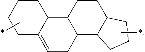
substituted or unsubstituted

substituted or unsubstituted
substituted or unsubstituted

substituted or unsubstituted

substituted or unsubstituted

substituted or unsubstituted

substituted or unsubstituted
substituted or unsubstituted
substituted or unsubstituted
substituted or unsubstituted
substituted or unsubstituted
substituted or unsubstituted

substituted or unsubstituted
substituted or unsubstituted

substituted or unsubstituted

substituted or unsubstituted
and substituted or unsubstituted

wherein at least one hydrogen in the substituted cyclic linking group is substituted with a C1-10-alkyl-*, F—*, Br—*, I—*, *—OH, *—NH2, or a C1-10-((meth)acryloxy)alkyl-*;
-
- *—Y is


wherein n is an integer of 0 to 5;
P1-SP1-MG-SP2-

and *—SP2-* is
wherein a and b are independently an integer of 0 to 2, each *-L-* is independently *—(CH2)c—*, *—O(CH2)c—*,
*—CH═CH—*, or *—C≡C—*, wherein c is an integer of 1 to 10, and *—Z—* is *—(CH2)d—* (wherein d is an integer of 0 to 12), and

wherein each A-* is independently H—*, a C1-10-alkyl-*, F—*, Br—*, I—*, *—OH, *—NH2, or *—CN; and

wherein each A-* is independently H—*, a C1-10-alkyl-*, F—*, Br—*, I—*, *—OH, *—NH2, or *—CN.


and
P1-SP1-MG-SP2-

and *—SP2-* is
wherein a and b are independently an integer of 0 to), each *-L-* is independently *—(CH2)c—*, *—O(CH2)c—*,
*—CH═CH—*, or *—C≡C—*, wherein c is an integer of 1 to 10, *—Z—* is *—(CH2)d—*, wherein d is an integer of 0 to 12, and *—Ar—*

wherein each A-* is independently H—*, a C1-10-alkyl-*, F—*, Br—*, I—*, *—OH, *—NH2, or *—CN; and
-
- *-MG-* is

wherein each A-* is independently H—*, a C1-10-alkyl-*, F—*, Br—*, I—*, *—OH, *—NH2, or *—CN.


*—CH═CH—*, or *—C≡C—*, wherein p1 is an integer of 1 to 10;
*—CH═CH—*, or *—C≡C—*, wherein p2 is an integer of 1 to 10;
*—CH═CH—*, or *—C≡C—*, wherein p3 is an integer of 1 to 10;

substituted or unsubstituted

substituted or unsubstituted

substituted or unsubstituted

substituted or unsubstituted

substituted or unsubstituted

substituted or unsubstituted
substituted or unsubstituted

substituted or unsubstituted

substituted or unsubstituted

substituted or unsubstituted

substituted or unsubstituted
substituted or unsubstituted
substituted or unsubstituted
substituted or unsubstituted
substituted or unsubstituted
substituted or unsubstituted

substituted or unsubstituted
substituted or unsubstituted

substituted or unsubstituted

substituted or unsubstituted
or substituted or unsubstituted

wherein at least one hydrogen in the substituted cyclic linking group is substituted with a C1-10-alkyl-*, F—*, Br—*, I*, *—OH, *—NH2, or a C1-10-((meth)acryloxy)alkyl-*; *—R—* is *—(CH2)q—*, *—O(CH2)q—*, *—(CH2)qArn-*, or *—O(CH2)qArn-*, wherein Arn is a substituted or unsubstituted C6-30 arylene, and q is an integer of 1 to 10, wherein at least one hydrogen in the substituted C6-30 arylene is substituted with a C1-10-alkyl-*, F—*, Br—*, I—*, *—OH, *—NH2, or a C1-10-((meth)acryloxy)alkyl-*;


wherein n is an integer of 0 to 5;
P1-SP1-MG-SP2-

and *—SP2-* is
wherein a and b are each independently an integer of 0 to 2, each ch *-L-* is independently *—(CH2)c—*, *—O(CH2)c—*,
*—CH═CH—*, or *—C≡C—*, wherein c is an integer of 1 to 10, *—Z—* is *—(CH2)d—*, wherein d is an integer of 0 to 12, and *—Ar—* is

wherein each A-* is independently H—*, a C1-10-alkyl-*, F—*, Br—*, I—*, *—OH, *—NH2, or *—CN;

wherein each A-* is independently H—*, a C1-10-alkyl-*, F—*, Br—*, I—*, *—OH, *—NH2, or *—CN; and


*—CH═CH—*, or *—C≡C—*, wherein p1 is an integer of 1 to 10;
*—CH═CH—*, or *—C≡C—*, wherein p2 is an integer of 1 to 10;
*—CH═CH—*, or *—C≡C—*, wherein p3 is an integer of 1 to 10;

substituted or unsubstituted

substituted or unsubstituted

substituted or unsubstituted

substituted or unsubstituted

substituted or unsubstituted

substituted or unsubstituted
substituted or unsubstituted

substituted or unsubstituted

substituted or unsubstituted

substituted or unsubstituted

substituted or unsubstituted
substituted or unsubstituted
substituted or unsubstituted
substituted or unsubstituted
substituted or unsubstituted
substituted or unsubstituted

substituted or unsubstituted
substituted or unsubstituted

substituted or unsubstituted

substituted or unsubstituted
or substituted or unsubstituted

wherein at least one hydrogen in the substituted cyclic linking group is substituted with a C1-10-alkyl-*, F—*, Br—*, I—*, *—OH, *—NH2, or a C1-10-((meth)acryloxy)alkyl-*;


(wherein n is an integer of 0 to 5);
P1-SP1-MG-SP2-

and *—SP2-* is
wherein a and b are independently an integer of 0 to 2, each *-L-* is independently *—(CH2)c—*, *—O(CH2)c—*,
*—CH═CH—*, or *—C≡C—*, wherein c is an integer of 1 to 10, *—Z—* is *—(CH2)d—*, wherein d is an integer of 0 to 12, and *—Ar—* is

wherein each A-* is independently H—*, a C1-10-alkyl-*, F—*, Br—*, I—*, *—OH, *—NH2, or *—CN; and

wherein each A-* is independently H—*, a C1-10-alkyl-*, F—*, Br—*, I—*, *—OH, *—NH2, or *—CN.


P1-SP1-MG-SP2-

*—SP1-* is
and *—SP2-* is
wherein a and b are independently an integer of 0 to 2, each *-L-* is independently *—(CH2)c—*, *—O(CH2)c—*,
*—CH═CH—*, or *—C≡C—*, wherein c is an integer of 1 to 10, *—Z—* is *—(CH2)d—*, wherein d is an integer of 0 to 12, and *—Ar—* is

wherein each A-* is independently H—*, a C1-10-alkyl-*, F—*, Br—*, I—*, *—OH, *—NH2, or *—CN; and *-MG-* is

wherein each A-* is independently H—*, a C1-10-alkyl-*, F—*, Br—*, I—*, *—OH, *—NH2, or *—CN.


and
P1-SP1-MG-SP2-

and *—SP2-* is
wherein a and b are independently an integer of 0 to 2, each *-L-* is independently *—(CH2)c—*, *—O(CH2)c—*,
*—CH═CH—*, or *—C≡C—*, wherein c is an integer of 1 to 10, *—Z—* is *—(CH2)d—*, wherein d is an integer of 0 to 12, and *—Ar—* is

wherein each A-* is independently H—*, a C1-10-alkyl-*, F—*, Br—*, I—*, *—OH, *—NH2, or *—CN; and *-MG-* is

wherein each A-* is independently H—*, a C1-10-alkyl-*, F—*, Br—*, I—*, *—OH, *—NH2, or *—CN.


*—CH═CH—*, or *—C≡C. p1 may be an integer of 1 to 10.
*—CH═CH—*, or *—C≡C. p2 may be an integer of 1 to 10.
*—CH═CH—*, or *—C≡C—*. p3 may be an integer of 1 to 10.

substituted or unsubstituted

substituted or unsubstituted

substituted or unsubstituted

substituted or unsubstituted

substituted or unsubstituted

substituted or unsubstituted
substituted or unsubstituted

substituted or unsubstituted

substituted or unsubstituted

substituted or unsubstituted

substituted or unsubstituted
substituted or unsubstituted
substituted or unsubstituted
substituted or unsubstituted
substituted or unsubstituted
substituted or unsubstituted

substituted or unsubstituted
substituted or unsubstituted

substituted or unsubstituted

substituted or unsubstituted
or substituted or unsubstituted


Here, n may be 0 to 5.
P1-SP1-MG-SP2-

(wherein a may be 0 to 2), and *—SP2-*, which is a linking group, may be
(wherein b may be 0 to 2). In

*—CH═CH—*, or *—C≡C—* (wherein c may be an integer of 1 to 10), and *—Z—* may be *—(CH2)d—* (wherein d may be an integer of 0 to 12). In each of *—SP1-* and *—SP2-*, *—Ar—*, which is a functional group for improving the miscibility with the


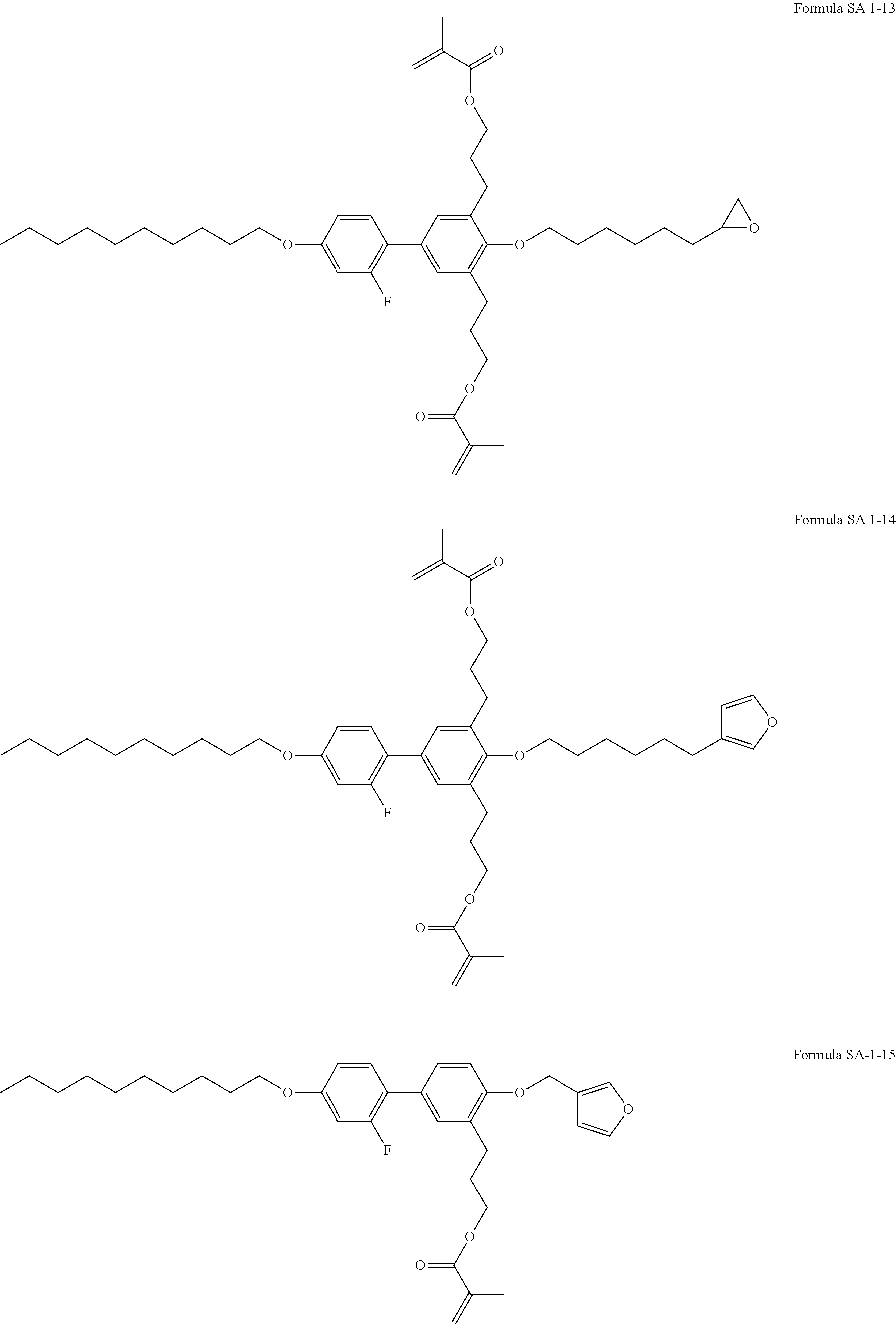


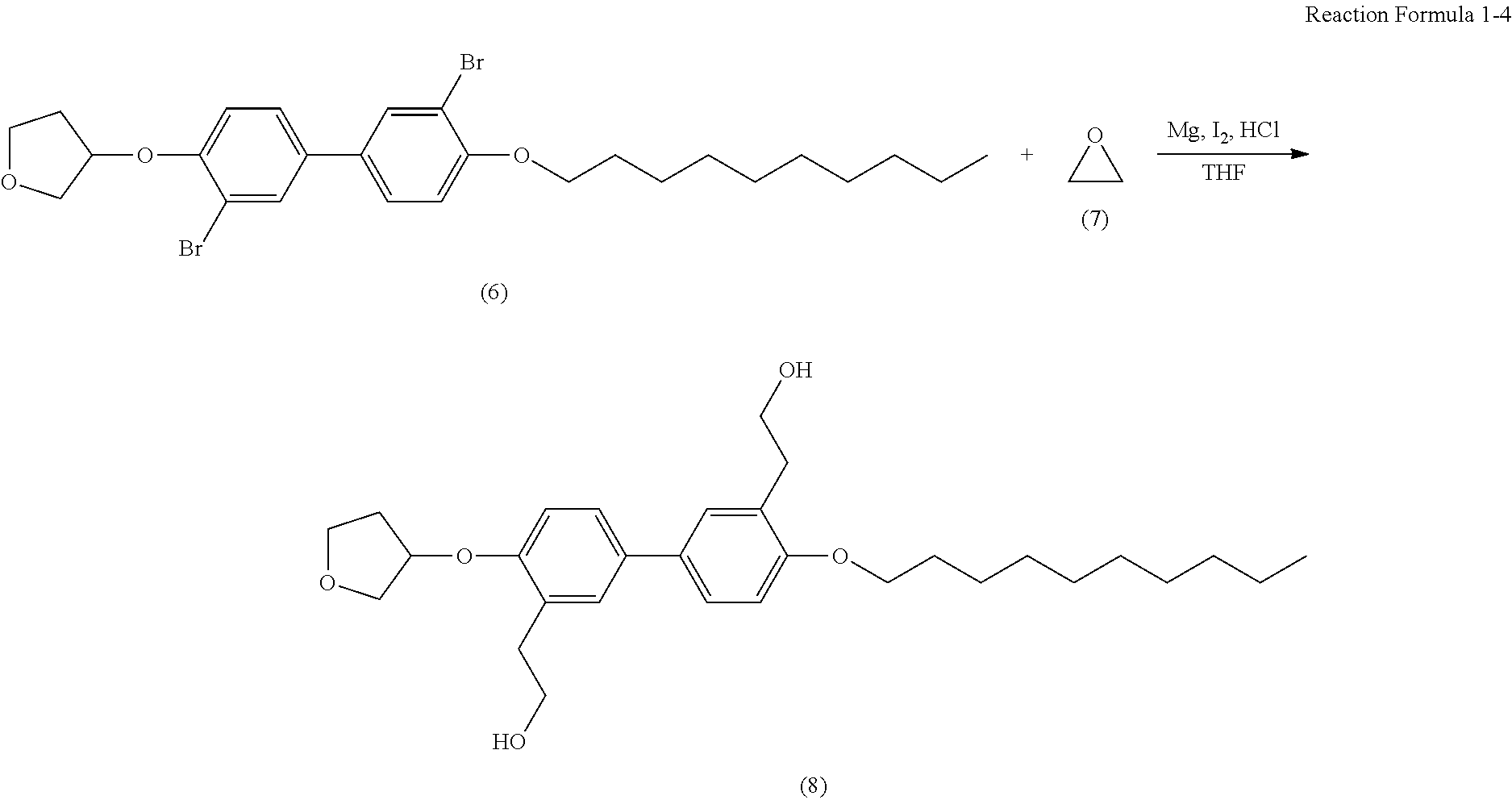


*—CH═CH—*, or *—C≡C—* Here, p1 may be an integer of 1 to 10.
*—CH═CH—*, or *—C≡C—*. Here, p2 may be an integer of 1 to 10.
*—CH═CH—*, or *—C≡C—*. Here, p3 may be an integer of 1 to 10.

substituted or unsubstituted

substituted or unsubstituted

substituted or unsubstituted

substituted or unsubstituted

substituted or unsubstituted

substituted or unsubstituted
substituted or unsubstituted

substituted or unsubstituted

substituted or unsubstituted

substituted or unsubstituted

substituted or unsubstituted
substituted or unsubstituted
substituted or unsubstituted
substituted or unsubstituted
substituted or unsubstituted
substituted or unsubstituted

substituted or unsubstituted
substituted or unsubstituted

substituted or unsubstituted

substituted or unsubstituted
or substituted or unsubstituted


Here, n may be 0 to 5.


| TABLE 1 | ||
| Voltage holding ratio (%) | ||
| Before | After | After fluorescent | ||
| exposure | UV exposure | UV exposure | ||
| Comparative Example 2 | 98.9 | 99.0 | 99.2 |
| Example 2-3 | 98.9 | 99.1 | 99.3 |
Claims (14)


P1-SP1-MG-SP2-P2 Formula 2


P1-SP1-MG-SP2-P2 Formula 2


P1-SP1-MG-SP2-P2 Formula 2


P1-SP1-MG-SP2-P2 Formula 2


P1-SP1-MG-SP2-P2 Formula 2


P1-SP1-MG-SP2-P2 Formula 2


Applications Claiming Priority (4)
| Application Number | Priority Date | Filing Date | Title |
|---|---|---|---|
| KR20160007512 | 2016-01-21 | ||
| KR10-2016-0007512 | 2016-01-21 | ||
| KR10-2016-0181120 | 2016-12-28 | ||
| KR1020160181120A KR20170088282A (en) | 2016-01-21 | 2016-12-28 | Liquid crystal composition, liquid crystal display device including the same and method for manufacturing liquid crystal display device including the same |
Publications (2)
| Publication Number | Publication Date |
|---|---|
| US20170210994A1 US20170210994A1 (en) | 2017-07-27 |
| US10190050B2 true US10190050B2 (en) | 2019-01-29 |
Family
ID=59360276
Family Applications (1)
| Application Number | Title | Priority Date | Filing Date |
|---|---|---|---|
| US15/408,958 Active US10190050B2 (en) | 2016-01-21 | 2017-01-18 | Liquid crystal composition, liquid crystal display device including the same, and method of manufacturing liquid crystal display device |
Country Status (2)
| Country | Link |
|---|---|
| US (1) | US10190050B2 (en) |
| CN (1) | CN106987255B (en) |
Cited By (3)
| Publication number | Priority date | Publication date | Assignee | Title |
|---|---|---|---|---|
| US11639327B2 (en) * | 2017-12-21 | 2023-05-02 | Dic Corporation | Polymerizable compound, and liquid crystal composition and liquid crystal display device using the same |
| US11739270B2 (en) | 2018-03-01 | 2023-08-29 | Dic Corporation | Polymerizable compound as well as liquid crystal composition and liquid crystal display device each including polymerizable compound |
| US11760934B2 (en) | 2017-11-17 | 2023-09-19 | Dic Corporation | Polymerizable compound, and liquid crystal composition and liquid crystal display element in which the compound is used |
Families Citing this family (9)
| Publication number | Priority date | Publication date | Assignee | Title |
|---|---|---|---|---|
| US10041001B2 (en) * | 2016-01-21 | 2018-08-07 | Samsung Display Co., Ltd. | Liquid crystal composition, liquid crystal display device including the same, and method of manufacturing liquid crystal display device |
| TWI737834B (en) * | 2016-10-26 | 2021-09-01 | 日商迪愛生股份有限公司 | Spontaneous alignment aid for liquid crystal composition |
| JPWO2018230322A1 (en) * | 2017-06-12 | 2019-11-14 | Dic株式会社 | Polymerizable compound and liquid crystal composition |
| KR102421946B1 (en) | 2017-11-23 | 2022-07-18 | 삼성디스플레이 주식회사 | Liquid crystal display device and method of manufacturing the same |
| CN108410475A (en) * | 2018-03-01 | 2018-08-17 | 深圳市华星光电半导体显示技术有限公司 | A kind of liquid crystal material and liquid crystal display panel |
| US11048125B2 (en) * | 2018-03-29 | 2021-06-29 | Sharp Kabushiki Kaisha | Liquid crystal cell and liquid crystal display device |
| CN108559528A (en) * | 2018-04-20 | 2018-09-21 | 深圳市华星光电半导体显示技术有限公司 | The preparation method of liquid crystal media mixture, liquid crystal display panel and liquid crystal display panel |
| JP7271896B2 (en) * | 2018-10-02 | 2023-05-12 | Dic株式会社 | Polymerizable compound, liquid crystal composition and liquid crystal display element using the same |
| US11518849B2 (en) * | 2020-05-22 | 2022-12-06 | International Business Machines Corporation | Post polymerization modification in flow |
Citations (10)
| Publication number | Priority date | Publication date | Assignee | Title |
|---|---|---|---|---|
| JP2004004329A (en) | 2002-05-31 | 2004-01-08 | Fujitsu Display Technologies Corp | Liquid crystal display device and method for manufacturing the same |
| US7248318B2 (en) | 2002-05-31 | 2007-07-24 | Sharp Kabushiki Kaisha | Liquid crystal display device and method of producing the same |
| US20130182202A1 (en) | 2010-09-25 | 2013-07-18 | Merck Patent Gesellschaft Mit Beschrankter Haftung | Liquid crystal displays and liquid crystalline media with homeotropic alignment |
| US20130215346A1 (en) | 2012-02-22 | 2013-08-22 | Pusan National University Industry-University Cooperation Foundation | Liquid crystal display |
| KR20140045535A (en) | 2011-07-07 | 2014-04-16 | 메르크 파텐트 게엠베하 | Liquid crystalline medium |
| US20160342029A1 (en) | 2015-05-22 | 2016-11-24 | Samsung Display Co., Ltd. | Liquid crystal display and manufacturing method thereof |
| KR20170019544A (en) | 2015-08-11 | 2017-02-22 | 삼성디스플레이 주식회사 | Curved liquid crystal display and method for manufacturing the same |
| KR20170029038A (en) | 2015-09-04 | 2017-03-15 | 삼성디스플레이 주식회사 | Liquid crystal display and method for manufacturing the same |
| KR20170032907A (en) | 2015-09-15 | 2017-03-24 | 삼성디스플레이 주식회사 | Composition for alignment layer, liquid crystal display comprising the composition and method for manufacturing the liquid crystal display |
| US20170210993A1 (en) * | 2016-01-21 | 2017-07-27 | Samsung Display Co. Ltd. | Liquid crystal composition, liquid crystal display device including the same, and method of manufacturing liquid crystal display device |
Family Cites Families (11)
| Publication number | Priority date | Publication date | Assignee | Title |
|---|---|---|---|---|
| JPS58136680A (en) * | 1982-02-05 | 1983-08-13 | Chisso Corp | Nematic liquid crystal composition |
| JPS5970684A (en) * | 1982-10-15 | 1984-04-21 | Chisso Corp | 5-substituted-1,3-dioxan-2-one |
| TWI306114B (en) * | 2002-04-09 | 2009-02-11 | Chisso Corp | Liquid cryatal compound having one terminal group being hydrogen atom, liquid crystal composition containing the same, and lcd device using the liquid crystal composition |
| JP4444774B2 (en) * | 2004-03-19 | 2010-03-31 | 富士フイルム株式会社 | Optically anisotropic material, liquid crystal display device and triphenylene compound |
| CN101013262B (en) * | 2007-02-07 | 2010-07-21 | 友达光电股份有限公司 | Photo-sensitive monomer, liquid crystal material, liquid crystal panel and method of fabrication, photoelectric device and fabricating method thereof |
| CN103080824B (en) * | 2010-09-07 | 2016-03-09 | 夏普株式会社 | Liquid crystal layer forms the manufacture method with composition, liquid crystal indicator and liquid crystal indicator |
| KR101926207B1 (en) * | 2011-02-05 | 2018-12-06 | 메르크 파텐트 게엠베하 | Liquid-crystal displays having homeotropic alignment |
| JP5929298B2 (en) * | 2011-03-02 | 2016-06-01 | Jnc株式会社 | Diamine, liquid crystal aligning agent, liquid crystal display element using the same, and method for forming liquid crystal alignment film |
| JP5879218B2 (en) * | 2012-07-03 | 2016-03-08 | 富士フイルム株式会社 | Pattern forming method, electronic device manufacturing method, actinic ray-sensitive or radiation-sensitive resin composition, and actinic ray-sensitive or radiation-sensitive film |
| JP6231293B2 (en) * | 2013-04-23 | 2017-11-15 | 富士フイルム株式会社 | Liquid crystal composition, retardation plate, circularly polarizing plate, and image display device |
| KR20150105564A (en) * | 2014-03-07 | 2015-09-17 | 삼성디스플레이 주식회사 | Liquid crystal display device, method of manufacturing the same and alignment layer composition |
-
2017
- 2017-01-18 US US15/408,958 patent/US10190050B2/en active Active
- 2017-01-19 CN CN201710043752.XA patent/CN106987255B/en not_active Expired - Fee Related
Patent Citations (16)
| Publication number | Priority date | Publication date | Assignee | Title |
|---|---|---|---|---|
| US7248318B2 (en) | 2002-05-31 | 2007-07-24 | Sharp Kabushiki Kaisha | Liquid crystal display device and method of producing the same |
| US20070206129A1 (en) | 2002-05-31 | 2007-09-06 | Kimiaki Nakamura | Liquid crystal display device and method of producing the same |
| US20120177847A1 (en) | 2002-05-31 | 2012-07-12 | Sharp Kabushiki Kaisha | Liquid crystal display device and method of producing the same |
| JP2004004329A (en) | 2002-05-31 | 2004-01-08 | Fujitsu Display Technologies Corp | Liquid crystal display device and method for manufacturing the same |
| KR20130110172A (en) | 2010-09-25 | 2013-10-08 | 메르크 파텐트 게엠베하 | Liquid crystal displays and liquid crystalline media with homeotropic alignment |
| US20130182202A1 (en) | 2010-09-25 | 2013-07-18 | Merck Patent Gesellschaft Mit Beschrankter Haftung | Liquid crystal displays and liquid crystalline media with homeotropic alignment |
| KR20140045535A (en) | 2011-07-07 | 2014-04-16 | 메르크 파텐트 게엠베하 | Liquid crystalline medium |
| US9234136B2 (en) | 2011-07-07 | 2016-01-12 | Merck Patent Gmbh | Liquid-crystalline medium |
| KR20130096456A (en) | 2012-02-22 | 2013-08-30 | 부산대학교 산학협력단 | Liquid crystal display |
| US20130215346A1 (en) | 2012-02-22 | 2013-08-22 | Pusan National University Industry-University Cooperation Foundation | Liquid crystal display |
| US20160342029A1 (en) | 2015-05-22 | 2016-11-24 | Samsung Display Co., Ltd. | Liquid crystal display and manufacturing method thereof |
| KR20160137871A (en) | 2015-05-22 | 2016-12-01 | 삼성디스플레이 주식회사 | Liquid crystal display and manufacturing method thereof |
| KR20170019544A (en) | 2015-08-11 | 2017-02-22 | 삼성디스플레이 주식회사 | Curved liquid crystal display and method for manufacturing the same |
| KR20170029038A (en) | 2015-09-04 | 2017-03-15 | 삼성디스플레이 주식회사 | Liquid crystal display and method for manufacturing the same |
| KR20170032907A (en) | 2015-09-15 | 2017-03-24 | 삼성디스플레이 주식회사 | Composition for alignment layer, liquid crystal display comprising the composition and method for manufacturing the liquid crystal display |
| US20170210993A1 (en) * | 2016-01-21 | 2017-07-27 | Samsung Display Co. Ltd. | Liquid crystal composition, liquid crystal display device including the same, and method of manufacturing liquid crystal display device |
Cited By (3)
| Publication number | Priority date | Publication date | Assignee | Title |
|---|---|---|---|---|
| US11760934B2 (en) | 2017-11-17 | 2023-09-19 | Dic Corporation | Polymerizable compound, and liquid crystal composition and liquid crystal display element in which the compound is used |
| US11639327B2 (en) * | 2017-12-21 | 2023-05-02 | Dic Corporation | Polymerizable compound, and liquid crystal composition and liquid crystal display device using the same |
| US11739270B2 (en) | 2018-03-01 | 2023-08-29 | Dic Corporation | Polymerizable compound as well as liquid crystal composition and liquid crystal display device each including polymerizable compound |
Also Published As
| Publication number | Publication date |
|---|---|
| CN106987255B (en) | 2022-04-15 |
| US20170210994A1 (en) | 2017-07-27 |
| CN106987255A (en) | 2017-07-28 |
Similar Documents
| Publication | Publication Date | Title |
|---|---|---|
| US10190050B2 (en) | Liquid crystal composition, liquid crystal display device including the same, and method of manufacturing liquid crystal display device | |
| US10041001B2 (en) | Liquid crystal composition, liquid crystal display device including the same, and method of manufacturing liquid crystal display device | |
| US11789302B2 (en) | Liquid crystal composition, light absorption anisotropic film, laminate, and image display device | |
| KR102296695B1 (en) | Phase difference material-forming resin composition, orientation material, and phase difference material | |
| US9139777B2 (en) | Composition of liquid crystal medium | |
| US10100201B2 (en) | Cured film formation composition, orientation material and retardation material | |
| JP5649779B2 (en) | Liquid crystalline composition and optical film | |
| JP6604483B2 (en) | Cured film forming composition, alignment material and retardation material | |
| US11066602B2 (en) | Reactive mesogen and liquid crystal composition including the same | |
| KR102280115B1 (en) | Liquid crystal aligning agent, liquid crystal aligning film and liquid crystal display element | |
| TW201809878A (en) | Liquid crystal aligning agent, liquid crystal alignment film and liquid crystal display element | |
| US10714665B2 (en) | Blue light blocking and light source | |
| US20170362508A1 (en) | Polymerizable compound and optically anisotropic body | |
| US20180244922A1 (en) | Liquid crystal aligning agent, liquid crystal alignment film, and liquid crystal display element | |
| KR102448661B1 (en) | Composition for production of liquid crystal alignment film for in-plane switching liquid crystal display element, liquid crystal alignment film using same, production method therefor, liquid crystal display element having liquid crystal alignment film, and production method therefor | |
| US10640708B2 (en) | Liquid crystal composition and liquid crystal display device including the same | |
| US20160033824A1 (en) | Alignment composition, liquid crystal display panel and method of manufacturing same | |
| KR20100069205A (en) | Uv curable resin composition, prism film, backlight unit and liquid crystal display device made by using the same | |
| US11697770B2 (en) | Liquid crystal composition, method for producing high-molecular weight liquid crystal compound, light absorption anisotropic film, laminate, and image display device | |
| US20210189239A1 (en) | Liquid crystal composition, retardation film, method for producing retardation film, transfer laminate, optical member, method for producing optical member, and display device | |
| US9115308B2 (en) | Liquid crystal medium composition of liquid crystal display | |
| US10061145B2 (en) | Liquid crystal display device | |
| US10457868B2 (en) | Liquid crystal composition and liquid crystal display including the same | |
| US20200148802A1 (en) | Method for the preparation of photoaligning polymer materials and compositions | |
| US20210363304A1 (en) | Optically clear resin composition, flexible optical film and image display device |
Legal Events
| Date | Code | Title | Description |
|---|---|---|---|
| AS | Assignment |
Owner name: SAMSUNG DISPLAY CO., LTD., KOREA, REPUBLIC OF Free format text: ASSIGNMENT OF ASSIGNORS INTEREST;ASSIGNORS:LIM, HO;AHN, HYUN KU;LYU, JAE JIN;REEL/FRAME:041181/0891 Effective date: 20170111 |
|
| STCF | Information on status: patent grant |
Free format text: PATENTED CASE |
|
| MAFP | Maintenance fee payment |
Free format text: PAYMENT OF MAINTENANCE FEE, 4TH YEAR, LARGE ENTITY (ORIGINAL EVENT CODE: M1551); ENTITY STATUS OF PATENT OWNER: LARGE ENTITY Year of fee payment: 4 |
|
| AS | Assignment |
Owner name: TCL CHINA STAR OPTOELECTRONICS TECHNOLOGY CO., LTD., CHINA Free format text: ASSIGNMENT OF ASSIGNORS INTEREST;ASSIGNOR:SAMSUNG DISPLAY CO., LTD.;REEL/FRAME:060778/0543 Effective date: 20220602 |