US9989809B2 - Curved liquid crystal display and method of manufacturing the same - Google Patents
Curved liquid crystal display and method of manufacturing the same Download PDFInfo
- Publication number
- US9989809B2 US9989809B2 US15/048,442 US201615048442A US9989809B2 US 9989809 B2 US9989809 B2 US 9989809B2 US 201615048442 A US201615048442 A US 201615048442A US 9989809 B2 US9989809 B2 US 9989809B2
- Authority
- US
- United States
- Prior art keywords
- liquid crystal
- curved
- alignment layer
- flat
- crystal alignment
- Prior art date
- Legal status (The legal status is an assumption and is not a legal conclusion. Google has not performed a legal analysis and makes no representation as to the accuracy of the status listed.)
- Active, expires
Links
- 0 CCCCCCOC(CC1)CCC1c(cc1)ccc1OC(C)(C)CC(C)(C)C(c1cc(NC*C)cc(N(C(C(C2C3C(N4c5cc(N(C(C(CC67)C(C(C8)C(N9c%10cc(N(C(CC%11C(C%12)C(CC(N%13c(cc%14)ccc%14N(C(C%14C(C(CC%15C(N%16*(C)=C)=O)C%16=O)C%15C%15C%14)=O)C%15=O)=O)C%11CC%13=O)=O)C%12=O)cc(C(OC(C)(C)CC(C)(C)Oc(cc%11)ccc%11C(c%11ccccc%11)=O)=O)c%10)=O)C6C8C9=O)=O)C7=O)cc(C(OC(C)(C)CC(C)(C)Oc6ccncc6)=O)c5)=O)C3C4=O)=O)C2=O)c1)=O Chemical compound CCCCCCOC(CC1)CCC1c(cc1)ccc1OC(C)(C)CC(C)(C)C(c1cc(NC*C)cc(N(C(C(C2C3C(N4c5cc(N(C(C(CC67)C(C(C8)C(N9c%10cc(N(C(CC%11C(C%12)C(CC(N%13c(cc%14)ccc%14N(C(C%14C(C(CC%15C(N%16*(C)=C)=O)C%16=O)C%15C%15C%14)=O)C%15=O)=O)C%11CC%13=O)=O)C%12=O)cc(C(OC(C)(C)CC(C)(C)Oc(cc%11)ccc%11C(c%11ccccc%11)=O)=O)c%10)=O)C6C8C9=O)=O)C7=O)cc(C(OC(C)(C)CC(C)(C)Oc6ccncc6)=O)c5)=O)C3C4=O)=O)C2=O)c1)=O 0.000 description 5
- LFXMVNUHQABLNF-MZCKTHBHSA-N CCCC1=CC=C(C2=CC=C(C3=CC=C(N)C=C3)C(F)=C2)C=C1.CCCC1=CC=C(C2=CC=C(C3=CC=C(O)C=C3)C(F)=C2)C=C1.CCCCC1=CC=C(C2=CC=C(O)C=C2)C=C1.CCCOC1=CC=C(C2=CC=C(O)C=C2)C(F)=C1F.CCC[C@H]1CC[C@H](OC(=O)[C@H]2CC[C@H](CCC/C=C\O)CC2)CC1.[H]C1([C@]2([H])CC[C@@H](O)CC2)CCC(CCCCC)CC1 Chemical compound CCCC1=CC=C(C2=CC=C(C3=CC=C(N)C=C3)C(F)=C2)C=C1.CCCC1=CC=C(C2=CC=C(C3=CC=C(O)C=C3)C(F)=C2)C=C1.CCCCC1=CC=C(C2=CC=C(O)C=C2)C=C1.CCCOC1=CC=C(C2=CC=C(O)C=C2)C(F)=C1F.CCC[C@H]1CC[C@H](OC(=O)[C@H]2CC[C@H](CCC/C=C\O)CC2)CC1.[H]C1([C@]2([H])CC[C@@H](O)CC2)CCC(CCCCC)CC1 LFXMVNUHQABLNF-MZCKTHBHSA-N 0.000 description 3
- ATDZZBDJMAKFQD-UGOMVITRSA-N CCCC1=CC=C(C2=CC=C(C3=CC=C(OC4=CC=NC=C4)C=C3)C=C2)C=C1.CCCCCCOC1=CC=C(C2=CC=C(OC3=CC=NC=C3)C=C2)C=C1.[H][C@@]12CC[C@]3([H])[C@]([H])(CC[C@@]4(C)[C@@]3([H])CCC[C@]4([H])C(C)(C)CC(C)C)[C@@]1(C)CC[C@H](OC1=CC=NC=C1)C2 Chemical compound CCCC1=CC=C(C2=CC=C(C3=CC=C(OC4=CC=NC=C4)C=C3)C=C2)C=C1.CCCCCCOC1=CC=C(C2=CC=C(OC3=CC=NC=C3)C=C2)C=C1.[H][C@@]12CC[C@]3([H])[C@]([H])(CC[C@@]4(C)[C@@]3([H])CCC[C@]4([H])C(C)(C)CC(C)C)[C@@]1(C)CC[C@H](OC1=CC=NC=C1)C2 ATDZZBDJMAKFQD-UGOMVITRSA-N 0.000 description 3
- YQPFSRBXWBEWGD-UHFFFAOYSA-N CCCCCCNCCN.CCCCOC1=CC=NC=C1 Chemical compound CCCCCCNCCN.CCCCOC1=CC=NC=C1 YQPFSRBXWBEWGD-UHFFFAOYSA-N 0.000 description 3
- ZPWNESHDEFDJDF-UHFFFAOYSA-N CCCCCCOC1CCC(C2=CC=C(OCOC(=O)C3=CC(NC)=CC(N4C(=O)C5C(C4=O)C4C(=O)N(C6=CC(N7C(=O)C8CC(C7=O)C7C9CC(C(=O)N(C%10=CC(N%11C(=O)CC%12C%13CC(=O)N(C%14=CC=C(N%15C(=O)C%16CC(C%15=O)C%15C%17CC(C(=O)N(C)C%17=O)C%16%15)C=C%14)C(=O)CC%13C%12CC%11=O)=CC(C(=O)OCOC%11=CC=C(C(=O)C%12=CC=CC=C%12)C=C%11)=C%10)C9=O)C87)=CC(C(=O)OCOC7=CC=NC=C7)=C6)C(=O)C54)=C3)C=C2)CC1.CCCCCCOC1CCC(C2=CC=C(OCOC(=O)C3=CC(NC)=CC(N4C(=O)C5CC(C4=O)C4C6CC(C(=O)N(C7=CC(N8C(=O)C9=CC%10=C(C=C9C8=O)C(=O)N(C8=CC(NC)=CC(C(=O)O)=C8)C%10=O)=CC(C(=O)OCOC8=CC=NC=C8)=C7)C6=O)C54)=C3)C=C2)CC1 Chemical compound CCCCCCOC1CCC(C2=CC=C(OCOC(=O)C3=CC(NC)=CC(N4C(=O)C5C(C4=O)C4C(=O)N(C6=CC(N7C(=O)C8CC(C7=O)C7C9CC(C(=O)N(C%10=CC(N%11C(=O)CC%12C%13CC(=O)N(C%14=CC=C(N%15C(=O)C%16CC(C%15=O)C%15C%17CC(C(=O)N(C)C%17=O)C%16%15)C=C%14)C(=O)CC%13C%12CC%11=O)=CC(C(=O)OCOC%11=CC=C(C(=O)C%12=CC=CC=C%12)C=C%11)=C%10)C9=O)C87)=CC(C(=O)OCOC7=CC=NC=C7)=C6)C(=O)C54)=C3)C=C2)CC1.CCCCCCOC1CCC(C2=CC=C(OCOC(=O)C3=CC(NC)=CC(N4C(=O)C5CC(C4=O)C4C6CC(C(=O)N(C7=CC(N8C(=O)C9=CC%10=C(C=C9C8=O)C(=O)N(C8=CC(NC)=CC(C(=O)O)=C8)C%10=O)=CC(C(=O)OCOC8=CC=NC=C8)=C7)C6=O)C54)=C3)C=C2)CC1 ZPWNESHDEFDJDF-UHFFFAOYSA-N 0.000 description 3
- JLMZZXJCTSLNQN-UHFFFAOYSA-N CCC(C)CCNCCN Chemical compound CCC(C)CCNCCN JLMZZXJCTSLNQN-UHFFFAOYSA-N 0.000 description 2
- MALFXIWPSGYIPG-DETGPAHYSA-N CCC(C)OC1=CC=NC=C1.CCCC1=CC=C(C2=CC=C(C3=CC=C(OC4=CC=NC=C4)C=C3)C=C2)C=C1.CCCCCCOC1=CC=C(C2=CC=C(OC3=CC=NC=C3)C=C2)C=C1.[H][C@@]12CC[C@]3([H])[C@]([H])(CC[C@@]4(C)[C@@]3([H])CCC[C@]4([H])C(C)(C)CC(C)C)[C@@]1(C)CC[C@H](OC1=CC=NC=C1)C2 Chemical compound CCC(C)OC1=CC=NC=C1.CCCC1=CC=C(C2=CC=C(C3=CC=C(OC4=CC=NC=C4)C=C3)C=C2)C=C1.CCCCCCOC1=CC=C(C2=CC=C(OC3=CC=NC=C3)C=C2)C=C1.[H][C@@]12CC[C@]3([H])[C@]([H])(CC[C@@]4(C)[C@@]3([H])CCC[C@]4([H])C(C)(C)CC(C)C)[C@@]1(C)CC[C@H](OC1=CC=NC=C1)C2 MALFXIWPSGYIPG-DETGPAHYSA-N 0.000 description 2
- IRVSPEUGCUPSOI-UHFFFAOYSA-N CCCC1=CC=C(C2=CC=C(C3=CC=C(C)C=C3)C(F)=C2)C=C1.CCCC1=CC=C(C2=CC=C(C3=CC=C(O)C=C3)C(F)=C2)C=C1.CCCCC1=CC=C(C2=CC=C(O)C=C2)C=C1.CCCOC1=CC=C(C2=CC=C(O)C=C2)C(F)=C1F Chemical compound CCCC1=CC=C(C2=CC=C(C3=CC=C(C)C=C3)C(F)=C2)C=C1.CCCC1=CC=C(C2=CC=C(C3=CC=C(O)C=C3)C(F)=C2)C=C1.CCCCC1=CC=C(C2=CC=C(O)C=C2)C=C1.CCCOC1=CC=C(C2=CC=C(O)C=C2)C(F)=C1F IRVSPEUGCUPSOI-UHFFFAOYSA-N 0.000 description 2
- DNSUBSJJAIFHIA-UHFFFAOYSA-N CCCCCCOC1CCC(C2=CC=C(OCC(=O)C3=CC(NC)=CC(N4C(=O)C5C(C4=O)C4C(=O)N(C6=CC(N7C(=O)C8CC(C7=O)C7C9CC(C(=O)N(C%10=CC(N%11C(=O)CC%12C%13CC(=O)N(C%14=CC=C(N%15C(=O)C%16CC(C%15=O)C%15C%17CC(C(=O)N(C)C%17=O)C%16%15)C=C%14)C(=O)CC%13C%12CC%11=O)=CC(C(=O)OCOC%11=CC=C(C(=O)C%12=CC=CC=C%12)C=C%11)=C%10)C9=O)C87)=CC(C(=O)OCOC7=CC=NC=C7)=C6)C(=O)C54)=C3)C=C2)CC1.CCCCCCOC1CCC(C2=CC=C(OCC(=O)C3=CC(NC)=CC(N4C(=O)C5CC(C4=O)C4C6CC(C(=O)N(C7=CC(N8C(=O)C9=CC%10=C(C=C9C8=O)C(=O)N(C8=CC(NC)=CC(C(=O)O)=C8)C%10=O)=CC(C(=O)OCOC8=CC=NC=C8)=C7)C6=O)C54)=C3)C=C2)CC1 Chemical compound CCCCCCOC1CCC(C2=CC=C(OCC(=O)C3=CC(NC)=CC(N4C(=O)C5C(C4=O)C4C(=O)N(C6=CC(N7C(=O)C8CC(C7=O)C7C9CC(C(=O)N(C%10=CC(N%11C(=O)CC%12C%13CC(=O)N(C%14=CC=C(N%15C(=O)C%16CC(C%15=O)C%15C%17CC(C(=O)N(C)C%17=O)C%16%15)C=C%14)C(=O)CC%13C%12CC%11=O)=CC(C(=O)OCOC%11=CC=C(C(=O)C%12=CC=CC=C%12)C=C%11)=C%10)C9=O)C87)=CC(C(=O)OCOC7=CC=NC=C7)=C6)C(=O)C54)=C3)C=C2)CC1.CCCCCCOC1CCC(C2=CC=C(OCC(=O)C3=CC(NC)=CC(N4C(=O)C5CC(C4=O)C4C6CC(C(=O)N(C7=CC(N8C(=O)C9=CC%10=C(C=C9C8=O)C(=O)N(C8=CC(NC)=CC(C(=O)O)=C8)C%10=O)=CC(C(=O)OCOC8=CC=NC=C8)=C7)C6=O)C54)=C3)C=C2)CC1 DNSUBSJJAIFHIA-UHFFFAOYSA-N 0.000 description 2
- UFSZTJZHYGULLV-UHFFFAOYSA-N C#CC.C#CC#CC.C=C(C)C(C)=O.C=CC.C=CC(C)=O.C=CCC(=O)OC.CCCC Chemical compound C#CC.C#CC#CC.C=C(C)C(C)=O.C=CC.C=CC(C)=O.C=CCC(=O)OC.CCCC UFSZTJZHYGULLV-UHFFFAOYSA-N 0.000 description 1
- KIUWDYOJDVQYOF-UHFFFAOYSA-N CC1=CC=C(N)C=C1.N/N=N/C1=CC(N)=CC(C(=O)O)=C1 Chemical compound CC1=CC=C(N)C=C1.N/N=N/C1=CC(N)=CC(C(=O)O)=C1 KIUWDYOJDVQYOF-UHFFFAOYSA-N 0.000 description 1
- HEJUBYKLBBPLDZ-DWNWNTTQSA-N CCCC1=CC=C(C2=CC=C(C3=CC=C(CCN)C=C3)C(F)=C2)C=C1.CCCC1=CC=C(C2=CC=C(C3=CC=C(OCCNCCCN)C=C3)C=C2F)C=C1.CCCC1=CC=C(C2=CC=C(C3=CC=C(OCCNCCOC)C=C3)C=C2F)C=C1.CCCC1=CC=C(C2=CC=C(C3=CC=C(OCCOCCOC)C=C3)C=C2F)C=C1.CCCCCC1=CC=C([C@H]2CC[C@H](C)CC2)C=C1.CCC[C@H]1CC[C@H](OC(=O)C2CCC(CCC/C=C\O)CC2)CC1.[H]C1([C@]2([H])CC[C@@H](O)CC2)CCC(CCC)CC1.[H]C1([C@]2([H])CC[C@@H](O)CC2)CCC(CCCCC)CC1.[H][C@@]12CC[C@]3([H])[C@]([H])(CC[C@@]4(C)[C@@]3([H])CCC[C@]4([H])[C@]([H])(C)CCCC(C)C)[C@@]1(C)CC[C@H](OCCCCCN)C2.[H][C@]1([C@]2([H])CC[C@@H](C(=O)OC3CCC(C4=CC=C(O)C=C4)CC3)CC2)CC[C@H](CCCCC)CC1 Chemical compound CCCC1=CC=C(C2=CC=C(C3=CC=C(CCN)C=C3)C(F)=C2)C=C1.CCCC1=CC=C(C2=CC=C(C3=CC=C(OCCNCCCN)C=C3)C=C2F)C=C1.CCCC1=CC=C(C2=CC=C(C3=CC=C(OCCNCCOC)C=C3)C=C2F)C=C1.CCCC1=CC=C(C2=CC=C(C3=CC=C(OCCOCCOC)C=C3)C=C2F)C=C1.CCCCCC1=CC=C([C@H]2CC[C@H](C)CC2)C=C1.CCC[C@H]1CC[C@H](OC(=O)C2CCC(CCC/C=C\O)CC2)CC1.[H]C1([C@]2([H])CC[C@@H](O)CC2)CCC(CCC)CC1.[H]C1([C@]2([H])CC[C@@H](O)CC2)CCC(CCCCC)CC1.[H][C@@]12CC[C@]3([H])[C@]([H])(CC[C@@]4(C)[C@@]3([H])CCC[C@]4([H])[C@]([H])(C)CCCC(C)C)[C@@]1(C)CC[C@H](OCCCCCN)C2.[H][C@]1([C@]2([H])CC[C@@H](C(=O)OC3CCC(C4=CC=C(O)C=C4)CC3)CC2)CC[C@H](CCCCC)CC1 HEJUBYKLBBPLDZ-DWNWNTTQSA-N 0.000 description 1
- HEJUBYKLBBPLDZ-UYWMKBNHSA-N CCCC1=CC=C(C2=CC=C(C3=CC=C(CCN)C=C3)C(F)=C2)C=C1.CCCC1=CC=C(C2=CC=C(C3=CC=C(OCCNCCCN)C=C3)C=C2F)C=C1.CCCC1=CC=C(C2=CC=C(C3=CC=C(OCCNCCOC)C=C3)C=C2F)C=C1.CCCC1=CC=C(C2=CC=C(C3=CC=C(OCCOCCOC)C=C3)C=C2F)C=C1.CCCCCC1=CC=C([C@H]2CC[C@H](C)CC2)C=C1.CCC[C@H]1CC[C@H](OC(=O)C2CCC(CCC/C=C\O)CC2)CC1.[H][C@@]12CC[C@]3([H])[C@]([H])(CC[C@@]4(C)[C@@]3([H])CCC[C@]4([H])[C@]([H])(C)CCCC(C)C)[C@@]1(C)CC[C@H](OCCCCCN)C2.[H][C@]1([C@]2([H])CC[C@@H](C(=O)OC3CCC(C4=CC=C(O)C=C4)CC3)CC2)CC[C@H](CCCCC)CC1.[H][C@]1([C@]2([H])CC[C@@H](CCC)CC2)CC[C@H](O)CC1.[H][C@]1([C@]2([H])CC[C@@H](CCCCC)CC2)CC[C@H](O)CC1 Chemical compound CCCC1=CC=C(C2=CC=C(C3=CC=C(CCN)C=C3)C(F)=C2)C=C1.CCCC1=CC=C(C2=CC=C(C3=CC=C(OCCNCCCN)C=C3)C=C2F)C=C1.CCCC1=CC=C(C2=CC=C(C3=CC=C(OCCNCCOC)C=C3)C=C2F)C=C1.CCCC1=CC=C(C2=CC=C(C3=CC=C(OCCOCCOC)C=C3)C=C2F)C=C1.CCCCCC1=CC=C([C@H]2CC[C@H](C)CC2)C=C1.CCC[C@H]1CC[C@H](OC(=O)C2CCC(CCC/C=C\O)CC2)CC1.[H][C@@]12CC[C@]3([H])[C@]([H])(CC[C@@]4(C)[C@@]3([H])CCC[C@]4([H])[C@]([H])(C)CCCC(C)C)[C@@]1(C)CC[C@H](OCCCCCN)C2.[H][C@]1([C@]2([H])CC[C@@H](C(=O)OC3CCC(C4=CC=C(O)C=C4)CC3)CC2)CC[C@H](CCCCC)CC1.[H][C@]1([C@]2([H])CC[C@@H](CCC)CC2)CC[C@H](O)CC1.[H][C@]1([C@]2([H])CC[C@@H](CCCCC)CC2)CC[C@H](O)CC1 HEJUBYKLBBPLDZ-UYWMKBNHSA-N 0.000 description 1
- XTGLURLWEJYCHW-RWNVVLGQSA-N CCCC1=CC=C(C2=CC=C(C3=CC=C(CCN)C=C3)C(F)=C2)C=C1.CCCC1=CC=C(C2=CC=C(C3=CC=C(OCCNCCCN)C=C3)C=C2F)C=C1.CCCC1=CC=C(C2=CC=C(C3=CC=C(OCCNCCOC)C=C3)C=C2F)C=C1.CCCC1=CC=C(C2=CC=C(C3=CC=C(OCCOCCOC)C=C3)C=C2F)C=C1.CCCCCC1=CC=C([C@H]2CC[C@H](C)CC2)C=C1.[H]C1([C@]2([H])CC[C@@H](O)CC2)CCC(CCC)CC1.[H][C@@]12CC[C@]3([H])[C@]([H])(CC[C@@]4(C)[C@@]3([H])CCC[C@]4([H])[C@]([H])(C)CCCC(C)C)[C@@]1(C)CC[C@H](OCCCCCN)C2.[H][C@]1([C@]2([H])CC[C@@H](C(=O)OC3CCC(C4=CC=C(O)C=C4)CC3)CC2)CC[C@H](CCCCC)CC1 Chemical compound CCCC1=CC=C(C2=CC=C(C3=CC=C(CCN)C=C3)C(F)=C2)C=C1.CCCC1=CC=C(C2=CC=C(C3=CC=C(OCCNCCCN)C=C3)C=C2F)C=C1.CCCC1=CC=C(C2=CC=C(C3=CC=C(OCCNCCOC)C=C3)C=C2F)C=C1.CCCC1=CC=C(C2=CC=C(C3=CC=C(OCCOCCOC)C=C3)C=C2F)C=C1.CCCCCC1=CC=C([C@H]2CC[C@H](C)CC2)C=C1.[H]C1([C@]2([H])CC[C@@H](O)CC2)CCC(CCC)CC1.[H][C@@]12CC[C@]3([H])[C@]([H])(CC[C@@]4(C)[C@@]3([H])CCC[C@]4([H])[C@]([H])(C)CCCC(C)C)[C@@]1(C)CC[C@H](OCCCCCN)C2.[H][C@]1([C@]2([H])CC[C@@H](C(=O)OC3CCC(C4=CC=C(O)C=C4)CC3)CC2)CC[C@H](CCCCC)CC1 XTGLURLWEJYCHW-RWNVVLGQSA-N 0.000 description 1
- XTGLURLWEJYCHW-VKXUDKCFSA-N CCCC1=CC=C(C2=CC=C(C3=CC=C(CCN)C=C3)C(F)=C2)C=C1.CCCC1=CC=C(C2=CC=C(C3=CC=C(OCCNCCCN)C=C3)C=C2F)C=C1.CCCC1=CC=C(C2=CC=C(C3=CC=C(OCCNCCOC)C=C3)C=C2F)C=C1.CCCC1=CC=C(C2=CC=C(C3=CC=C(OCCOCCOC)C=C3)C=C2F)C=C1.CCCCCC1=CC=C([C@H]2CC[C@H](C)CC2)C=C1.[H]C12CC[C@@]3([H])C[C@@H](OCCCCCN)CC[C@]3(C)[C@@]1([H])CC[C@@]1(C)[C@@]2([H])CCC[C@]1([H])[C@]([H])(C)CCCC(C)C.[H][C@]1([C@]2([H])CC[C@@H](C(=O)OC3CCC(C4=CC=C(O)C=C4)CC3)CC2)CC[C@H](CCCCC)CC1.[H][C@]1([C@]2([H])CC[C@@H](CCC)CC2)CC[C@H](O)CC1 Chemical compound CCCC1=CC=C(C2=CC=C(C3=CC=C(CCN)C=C3)C(F)=C2)C=C1.CCCC1=CC=C(C2=CC=C(C3=CC=C(OCCNCCCN)C=C3)C=C2F)C=C1.CCCC1=CC=C(C2=CC=C(C3=CC=C(OCCNCCOC)C=C3)C=C2F)C=C1.CCCC1=CC=C(C2=CC=C(C3=CC=C(OCCOCCOC)C=C3)C=C2F)C=C1.CCCCCC1=CC=C([C@H]2CC[C@H](C)CC2)C=C1.[H]C12CC[C@@]3([H])C[C@@H](OCCCCCN)CC[C@]3(C)[C@@]1([H])CC[C@@]1(C)[C@@]2([H])CCC[C@]1([H])[C@]([H])(C)CCCC(C)C.[H][C@]1([C@]2([H])CC[C@@H](C(=O)OC3CCC(C4=CC=C(O)C=C4)CC3)CC2)CC[C@H](CCCCC)CC1.[H][C@]1([C@]2([H])CC[C@@H](CCC)CC2)CC[C@H](O)CC1 XTGLURLWEJYCHW-VKXUDKCFSA-N 0.000 description 1
- XTGLURLWEJYCHW-RDNFAFHFSA-N CCCC1=CC=C(C2=CC=C(C3=CC=C(CCN)C=C3)C(F)=C2)C=C1.CCCC1=CC=C(C2=CC=C(C3=CC=C(OCCNCCCN)C=C3)C=C2F)C=C1.CCCC1=CC=C(C2=CC=C(C3=CC=C(OCCNCCOC)C=C3)C=C2F)C=C1.CCCC1=CC=C(C2=CC=C(C3=CC=C(OCCOCCOC)C=C3)C=C2F)C=C1.CCCCCC1=CC=C([C@H]2CC[C@H](C)CC2)C=C1.[H][C@@]12CC[C@]3([H])[C@]([H])(CC[C@@]4(C)[C@@]3([H])CCC[C@]4([H])[C@]([H])(C)CCCC(C)C)[C@@]1(C)CC[C@H](OCCCCCN)C2.[H][C@]1([C@]2([H])CC[C@@H](C(=O)OC3CCC(C4=CC=C(O)C=C4)CC3)CC2)CC[C@H](CCCCC)CC1.[H][C@]1([C@]2([H])CC[C@@H](CCC)CC2)CC[C@H](O)CC1 Chemical compound CCCC1=CC=C(C2=CC=C(C3=CC=C(CCN)C=C3)C(F)=C2)C=C1.CCCC1=CC=C(C2=CC=C(C3=CC=C(OCCNCCCN)C=C3)C=C2F)C=C1.CCCC1=CC=C(C2=CC=C(C3=CC=C(OCCNCCOC)C=C3)C=C2F)C=C1.CCCC1=CC=C(C2=CC=C(C3=CC=C(OCCOCCOC)C=C3)C=C2F)C=C1.CCCCCC1=CC=C([C@H]2CC[C@H](C)CC2)C=C1.[H][C@@]12CC[C@]3([H])[C@]([H])(CC[C@@]4(C)[C@@]3([H])CCC[C@]4([H])[C@]([H])(C)CCCC(C)C)[C@@]1(C)CC[C@H](OCCCCCN)C2.[H][C@]1([C@]2([H])CC[C@@H](C(=O)OC3CCC(C4=CC=C(O)C=C4)CC3)CC2)CC[C@H](CCCCC)CC1.[H][C@]1([C@]2([H])CC[C@@H](CCC)CC2)CC[C@H](O)CC1 XTGLURLWEJYCHW-RDNFAFHFSA-N 0.000 description 1
- YWIPODFHMBUJQD-UHFFFAOYSA-N CCCCCCOC1CCC(C2=CC=C(OCOC(=O)C3=CC(C)=CC(N)=C3)C=C2)CC1.N/N=N/C1=CC(N)=CC(C(=O)OCOC2=CC=C(C(=O)C3=CC=CC=C3)C=C2)=C1.N/N=N/C1=CC(N)=CC(C(=O)OCOC2=CC=NC=C2)=C1 Chemical compound CCCCCCOC1CCC(C2=CC=C(OCOC(=O)C3=CC(C)=CC(N)=C3)C=C2)CC1.N/N=N/C1=CC(N)=CC(C(=O)OCOC2=CC=C(C(=O)C3=CC=CC=C3)C=C2)=C1.N/N=N/C1=CC(N)=CC(C(=O)OCOC2=CC=NC=C2)=C1 YWIPODFHMBUJQD-UHFFFAOYSA-N 0.000 description 1
- YKDZEZADFLISTJ-UHFFFAOYSA-N O=C1OC(=O)C2=C1/C=C1/C(=O)OC(=O)/C1=C/2.O=C1OC(=O)C2C1C1C(=O)OC(=O)C21.O=C1OC(=O)C2CC1C1C2C2C3CC(C(=O)OC3=O)C12 Chemical compound O=C1OC(=O)C2=C1/C=C1/C(=O)OC(=O)/C1=C/2.O=C1OC(=O)C2C1C1C(=O)OC(=O)C21.O=C1OC(=O)C2CC1C1C2C2C3CC(C(=O)OC3=O)C12 YKDZEZADFLISTJ-UHFFFAOYSA-N 0.000 description 1
Images


Classifications
-
- G—PHYSICS
- G02—OPTICS
- G02F—OPTICAL DEVICES OR ARRANGEMENTS FOR THE CONTROL OF LIGHT BY MODIFICATION OF THE OPTICAL PROPERTIES OF THE MEDIA OF THE ELEMENTS INVOLVED THEREIN; NON-LINEAR OPTICS; FREQUENCY-CHANGING OF LIGHT; OPTICAL LOGIC ELEMENTS; OPTICAL ANALOGUE/DIGITAL CONVERTERS
- G02F1/00—Devices or arrangements for the control of the intensity, colour, phase, polarisation or direction of light arriving from an independent light source, e.g. switching, gating or modulating; Non-linear optics
- G02F1/01—Devices or arrangements for the control of the intensity, colour, phase, polarisation or direction of light arriving from an independent light source, e.g. switching, gating or modulating; Non-linear optics for the control of the intensity, phase, polarisation or colour
- G02F1/13—Devices or arrangements for the control of the intensity, colour, phase, polarisation or direction of light arriving from an independent light source, e.g. switching, gating or modulating; Non-linear optics for the control of the intensity, phase, polarisation or colour based on liquid crystals, e.g. single liquid crystal display cells
- G02F1/133—Constructional arrangements; Operation of liquid crystal cells; Circuit arrangements
- G02F1/1333—Constructional arrangements; Manufacturing methods
- G02F1/1337—Surface-induced orientation of the liquid crystal molecules, e.g. by alignment layers
- G02F1/133711—Surface-induced orientation of the liquid crystal molecules, e.g. by alignment layers by organic films, e.g. polymeric films
-
- C—CHEMISTRY; METALLURGY
- C09—DYES; PAINTS; POLISHES; NATURAL RESINS; ADHESIVES; COMPOSITIONS NOT OTHERWISE PROVIDED FOR; APPLICATIONS OF MATERIALS NOT OTHERWISE PROVIDED FOR
- C09K—MATERIALS FOR MISCELLANEOUS APPLICATIONS, NOT PROVIDED FOR ELSEWHERE
- C09K19/00—Liquid crystal materials
- C09K19/52—Liquid crystal materials characterised by components which are not liquid crystals, e.g. additives with special physical aspect: solvents, solid particles
- C09K19/54—Additives having no specific mesophase characterised by their chemical composition
- C09K19/56—Aligning agents
-
- C—CHEMISTRY; METALLURGY
- C09—DYES; PAINTS; POLISHES; NATURAL RESINS; ADHESIVES; COMPOSITIONS NOT OTHERWISE PROVIDED FOR; APPLICATIONS OF MATERIALS NOT OTHERWISE PROVIDED FOR
- C09K—MATERIALS FOR MISCELLANEOUS APPLICATIONS, NOT PROVIDED FOR ELSEWHERE
- C09K2323/00—Functional layers of liquid crystal optical display excluding electroactive liquid crystal layer characterised by chemical composition
- C09K2323/02—Alignment layer characterised by chemical composition
-
- G—PHYSICS
- G02—OPTICS
- G02F—OPTICAL DEVICES OR ARRANGEMENTS FOR THE CONTROL OF LIGHT BY MODIFICATION OF THE OPTICAL PROPERTIES OF THE MEDIA OF THE ELEMENTS INVOLVED THEREIN; NON-LINEAR OPTICS; FREQUENCY-CHANGING OF LIGHT; OPTICAL LOGIC ELEMENTS; OPTICAL ANALOGUE/DIGITAL CONVERTERS
- G02F1/00—Devices or arrangements for the control of the intensity, colour, phase, polarisation or direction of light arriving from an independent light source, e.g. switching, gating or modulating; Non-linear optics
- G02F1/01—Devices or arrangements for the control of the intensity, colour, phase, polarisation or direction of light arriving from an independent light source, e.g. switching, gating or modulating; Non-linear optics for the control of the intensity, phase, polarisation or colour
- G02F1/13—Devices or arrangements for the control of the intensity, colour, phase, polarisation or direction of light arriving from an independent light source, e.g. switching, gating or modulating; Non-linear optics for the control of the intensity, phase, polarisation or colour based on liquid crystals, e.g. single liquid crystal display cells
- G02F1/133—Constructional arrangements; Operation of liquid crystal cells; Circuit arrangements
- G02F1/1333—Constructional arrangements; Manufacturing methods
- G02F1/1337—Surface-induced orientation of the liquid crystal molecules, e.g. by alignment layers
- G02F1/133711—Surface-induced orientation of the liquid crystal molecules, e.g. by alignment layers by organic films, e.g. polymeric films
- G02F1/133726—Surface-induced orientation of the liquid crystal molecules, e.g. by alignment layers by organic films, e.g. polymeric films made of a mesogenic material
-
- G—PHYSICS
- G02—OPTICS
- G02F—OPTICAL DEVICES OR ARRANGEMENTS FOR THE CONTROL OF LIGHT BY MODIFICATION OF THE OPTICAL PROPERTIES OF THE MEDIA OF THE ELEMENTS INVOLVED THEREIN; NON-LINEAR OPTICS; FREQUENCY-CHANGING OF LIGHT; OPTICAL LOGIC ELEMENTS; OPTICAL ANALOGUE/DIGITAL CONVERTERS
- G02F1/00—Devices or arrangements for the control of the intensity, colour, phase, polarisation or direction of light arriving from an independent light source, e.g. switching, gating or modulating; Non-linear optics
- G02F1/01—Devices or arrangements for the control of the intensity, colour, phase, polarisation or direction of light arriving from an independent light source, e.g. switching, gating or modulating; Non-linear optics for the control of the intensity, phase, polarisation or colour
- G02F1/13—Devices or arrangements for the control of the intensity, colour, phase, polarisation or direction of light arriving from an independent light source, e.g. switching, gating or modulating; Non-linear optics for the control of the intensity, phase, polarisation or colour based on liquid crystals, e.g. single liquid crystal display cells
- G02F1/133—Constructional arrangements; Operation of liquid crystal cells; Circuit arrangements
- G02F1/1333—Constructional arrangements; Manufacturing methods
- G02F1/1337—Surface-induced orientation of the liquid crystal molecules, e.g. by alignment layers
- G02F1/133742—Surface-induced orientation of the liquid crystal molecules, e.g. by alignment layers for homeotropic alignment
-
- G—PHYSICS
- G02—OPTICS
- G02F—OPTICAL DEVICES OR ARRANGEMENTS FOR THE CONTROL OF LIGHT BY MODIFICATION OF THE OPTICAL PROPERTIES OF THE MEDIA OF THE ELEMENTS INVOLVED THEREIN; NON-LINEAR OPTICS; FREQUENCY-CHANGING OF LIGHT; OPTICAL LOGIC ELEMENTS; OPTICAL ANALOGUE/DIGITAL CONVERTERS
- G02F1/00—Devices or arrangements for the control of the intensity, colour, phase, polarisation or direction of light arriving from an independent light source, e.g. switching, gating or modulating; Non-linear optics
- G02F1/01—Devices or arrangements for the control of the intensity, colour, phase, polarisation or direction of light arriving from an independent light source, e.g. switching, gating or modulating; Non-linear optics for the control of the intensity, phase, polarisation or colour
- G02F1/13—Devices or arrangements for the control of the intensity, colour, phase, polarisation or direction of light arriving from an independent light source, e.g. switching, gating or modulating; Non-linear optics for the control of the intensity, phase, polarisation or colour based on liquid crystals, e.g. single liquid crystal display cells
- G02F1/133—Constructional arrangements; Operation of liquid crystal cells; Circuit arrangements
- G02F1/1333—Constructional arrangements; Manufacturing methods
- G02F1/1337—Surface-induced orientation of the liquid crystal molecules, e.g. by alignment layers
- G02F1/13378—Surface-induced orientation of the liquid crystal molecules, e.g. by alignment layers by treatment of the surface, e.g. embossing, rubbing or light irradiation
- G02F1/133788—Surface-induced orientation of the liquid crystal molecules, e.g. by alignment layers by treatment of the surface, e.g. embossing, rubbing or light irradiation by light irradiation, e.g. linearly polarised light photo-polymerisation
-
- G02F2001/133726—
-
- G02F2001/133742—
-
- Y10T428/10—
-
- Y10T428/1005—
Definitions
- the present invention relates to a curved liquid crystal display and a method of manufacturing the same.
- a liquid crystal display is a type of flat panel display that is widely used.
- a liquid crystal display includes two substrates on which field generating electrodes, such as a pixel electrode and a common electrode are formed, and a liquid crystal layer interposed between the two substrates.
- a liquid crystal display displays an image when a voltage is applied to field generating electrodes to produce an electric field in the liquid crystal layer, whereby the alignment direction of liquid crystals in the liquid crystal layer is determined and the polarization of incident light is controlled.
- a liquid crystal display may have a large screen size when used as a display device for a television receiver. As the size of the liquid crystal display is, the quality of the images displayed at the center of the screen and at opposite ends of the screen may appear different from each other when viewed by a viewer.
- a liquid crystal display may be curved to have a concave or convex shape.
- a curved liquid crystal display may be provided in a portrait form, which is curved in a longitudinal direction and has a length greater than its width when viewed by viewers, or in a landscape form, which is curved in a transverse direction and has a length shorter than its width.
- aspects of the invention provide a curved liquid crystal display having increased light transmittance and a method of manufacturing the same.
- aspects of the invention also provide a curved liquid crystal display, which may prevent the generation of unnecessary patterns or stains due to the use of a curved panel, and a method of manufacturing the same.
- a curved liquid crystal display includes a first curved substrate; a second curved substrate facing the first curved substrate; a liquid crystal layer disposed between the first curved substrate and the second curved substrate; a first curved liquid crystal alignment layer disposed between the liquid crystal layer and the first curved substrate and including at least one vertical alignment functional group represented by Chemical Formulae 1 to 5 below; and a second curved liquid crystal alignment layer disposed between the liquid crystal layer and the second curved substrate:
- X is H, F, Br, I, OH, C 3 H 7 , NH 2 , or CN, and in Chemical Formula 5, n is a natural number of 1 to 20.
- the second curved liquid crystal alignment layer may contain a polymerization initiator.
- the first curved liquid crystal alignment layer may contain no polymerization initiator.
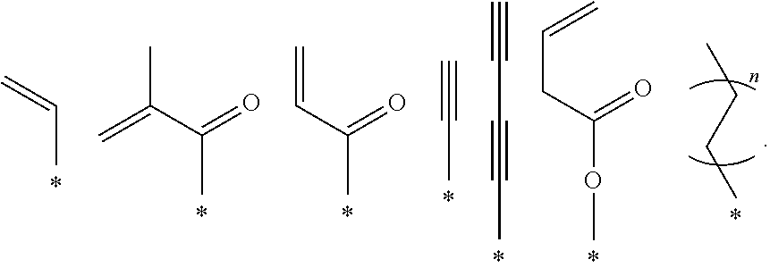
- the first curved liquid crystal alignment layer may further include at least one vertical alignment functional group represented by Chemical Formulae 6 to 19 below.
- the second curved liquid crystal alignment layer may include a repeating unit as represented by Chemical Formulae 29 and 30 below:
- each n is independently a natural number of 1 to 20.
- the second curved liquid crystal alignment layer may include a reactive mesogen and have a higher reactive mesogen content than the first curved liquid crystal alignment layer.
- the curved liquid crystal display, the second curved liquid crystal alignment layer may have a multilayer structure comprising a 2-1 st curved liquid crystal alignment layer and a 2-2 nd curved liquid crystal alignment layer, and the 2-2 nd curved liquid crystal alignment layer may have a higher reactive mesogen content than the 2-1 st curved liquid crystal alignment layer.
- the liquid crystal layer may comprise a first liquid crystal molecule having negative dielectric anisotropy aligned on a surface of the first curved liquid crystal alignment layer, and a second liquid crystal molecule aligned on a surface of the second curved liquid crystal alignment layer, and the first liquid crystal molecule may be vertically aligned compared to the second liquid crystal molecule when an electric field is not applied.
- the curved liquid crystal display may further includes a patternless electrode disposed between the first curved substrate and the first curved liquid crystal alignment layer and having no slit pattern; and a pattern electrode disposed between the second curved liquid crystal alignment layer and the second curved substrate and having a slit pattern.
- a method of manufacturing a curved liquid crystal display includes, preparing a first flat substrate and a second flat substrate facing each other; forming a second flat liquid crystal alignment layer on a surface of the second flat substrate that faces the first flat substrate; injecting a liquid crystal between the first flat substrate and the second flat substrate; radiating ultraviolet (UV) light toward at least one of the first flat substrate and the second flat substrate when an electric field is applied; and curving the first flat substrate and the second flat substrate, wherein the liquid crystal layer includes at least one of vertical alignment functional groups represented by Chemical Formulae 1 to 5 below:
- X is H, F, Br, I, OH, C 3 H 7 , NH 2 , or CN, and in Chemical Formula 5, n is a natural number of 1 to 20.
- the liquid crystal layer may further include at least one vertical alignment functional group represented by Chemical Formulae 6 to 19 below.
- the vertical alignment functional group may enable a first flat liquid crystal alignment layer to be formed on a surface of the first flat substrate that faces the second flat substrate.
- the second flat liquid crystal alignment layer may include a polymerization initiator.
- the second flat liquid crystal alignment layer may include a repeating unit as represented by Chemical Formulae 29 and 30 below:
- each n is independently a natural number of 1 to 20.
- At least one of the liquid crystal layer and the second flat liquid crystal alignment layer may further include a reactive mesogen.
- the second flat liquid crystal alignment layer in the radiating the UV light, may be formed into a multilayer structure comprising a 2-1 st flat liquid crystal alignment layer and a 2-2 nd flat liquid crystal alignment layer having higher reactive mesogen content than the 2-1 st flat liquid crystal alignment layer.
- the liquid crystal layer may include a first liquid crystal molecule having negative dielectric anisotropy aligned on a surface of the first flat liquid crystal alignment layer, and a second liquid crystal molecule aligned on a surface of the second flat liquid crystal alignment layer, and the first liquid crystal molecule is vertically aligned compared to the second liquid crystal molecule when the applied electric field is removed after the radiating the UV light.
- the method of manufacturing curved liquid crystal display may further include forming a patternless electrode disposed between the first flat substrate and the first flat liquid crystal alignment layer, the patternless electrode having no slit pattern; and forming a pattern electrode disposed between the second flat liquid crystal alignment layer and the second flat substrate, the pattern electrode having a slit pattern.
- the method of manufacturing curved liquid crystal display may further include radiating fluorescent UV light after the radiating of the UV light.
- the method of manufacturing curved liquid crystal display may further include annealing at least one of the first flat substrate and the second flat substrate using heat after the liquid crystal is injected.
- FIG. 1 is an exploded perspective view schematically showing an exemplary embodiment of a curved liquid crystal display
- FIG. 2 is a schematic enlarged view of Part II in FIG. 1 ;
- FIG. 3 is a schematic cross-sectional view taken along line III-III′ of FIG. 1 ;
- FIGS. 4 to 9 are cross-sectional views schematically showing an exemplary process of manufacturing a curved liquid crystal display.
- inventive concept may, however, be embodied in many different forms and should not be construed as being limited to the embodiments set forth herein. Rather, these embodiments are provided so that this disclosure will be thorough and complete and will fully convey the concept of the inventive concept to those skilled in the art, and the inventive concept will only be defined by the appended claims.
- first, second, third, etc. may be used herein to describe various elements, components, regions, layers and/or sections, these elements, components, regions, layers and/or sections should not be limited by these terms. These terms are only used to distinguish one element, component, region, layer or section from another element, component, region, layer or section. Thus, a first element, component, region, layer or section discussed below could be termed a second element, component, region, layer or section without departing from the teachings of the invention.
- spatially relative terms such as “bottom,” “below,” “lower,” “under,” “above,” “upper,” “top” and the like, may be used herein for ease of description to describe the relationship of one element or feature to another element(s) or feature(s) as illustrated in the figures. It will be understood that the spatially relative terms are intended to encompass different orientations of the device in use or operation, in addition to the orientation depicted in the figures. For example, if the device in the figures is turned over, elements described as “below” or “beneath” relative to other elements or features would then be oriented “above” relative to the other elements or features. Thus, the exemplary term “below” can encompass both an orientation of above and below. The device may be otherwise oriented (rotated 90 degrees or at other orientations) and the spatially relative descriptors used herein interpreted accordingly.
- “About” or “approximately” as used herein is inclusive of the stated value and means within an acceptable range of deviation for the particular value as determined by one of ordinary skill in the art, considering the measurement in question and the error associated with measurement of the particular quantity (i.e., the limitations of the measurement system). For example, “about” can mean within one or more standard deviations, or within ⁇ 30%, 20%, 10%, 5% of the stated value.”
- Exemplary embodiments are described herein with reference to cross section illustrations that are schematic illustrations of idealized embodiments. As such, variations from the shapes of the illustrations as a result, for example, of manufacturing techniques and/or tolerances, are to be expected. Thus, embodiments described herein should not be construed as limited to the particular shapes of regions as illustrated herein but are to include deviations in shapes that result, for example, from manufacturing. For example, a region illustrated or described as flat may, typically, have rough and/or nonlinear features. Moreover, sharp angles that are illustrated may be rounded. Thus, the regions illustrated in the figures are schematic in nature and their shapes are not intended to illustrate the precise shape of a region and are not intended to limit the scope of the present claims.
- FIG. 1 is an exploded perspective view schematically showing an exemplary embodiment of a curved liquid crystal display 500 C
- FIG. 2 is a schematic enlarged view of Part II of FIG. 1 .
- the exemplary curved liquid crystal display 500 C includes a first curved substrate 100 C, a second curved substrate 200 C configured to face the first curved substrate 100 C and spaced apart therefrom, and a liquid crystal layer 300 C interposed between the first curved substrate 100 C and the second curved substrate 200 C.
- the first and the second curved substrate 100 C, 200 C each include a display area DAC and a non-display area NDAC.
- the display area (DAC) is an area where an image is viewed
- the non-display area NDAC is an area where an image is not viewed.
- the outer periphery of the display area DAC is enclosed with the non-display area NDAC.
- a common electrode 110 C may be disposed between the first curved substrate 100 C and the second curved substrate 200 C, and may be a patternless electrode having no slit pattern.
- a pixel electrode 291 C may be disposed between the second curved substrate 200 C and the common electrode 110 C, and may be a pattern electrode having a slit pattern.
- the liquid crystal layer 300 C may be disposed between the common electrode 110 C and the pixel electrode 291 C.
- the liquid crystal layer 300 C may contain liquid crystal molecules LC having negative dielectric anisotropy.
- a first curved liquid crystal alignment layer AL 1 C may be disposed between the common electrode 110 C and the liquid crystal layer 300 C.
- a second curved liquid crystal alignment layer AL 2 C may be disposed between the pixel electrode 291 C and the liquid crystal layer 300 C.
- the second curved substrate 200 C may be a thin film transistor substrate.
- a plurality of gate lines GLC extending in a first direction and a plurality of data lines DLC extending in a second direction perpendicular to the first direction may be formed.
- the pixel electrode 291 C may be disposed at each of pixels PXC defined by the gate lines GLC and the data lines DLC.
- the pixel electrode 291 C may include sub-pixel electrodes 291 - 1 C, 291 - 2 C, which are spaced apart from each other.
- individual sub-pixel electrodes 291 - 1 C, 291 - 2 C may have a rectangular shape.
- Individual sub-pixel electrodes 291 - 1 C, 291 - 2 C may be pattern electrodes having a slit pattern.
- the slit pattern may be configured such that a dissection part DC may be disposed between a stem part SC and a branch part BC extending therefrom.
- the stem part SC may be provided in a cross (+) shaped form
- the branch part BC may be radially provided in a direction of about 45° from the stem part SC in cross (+) shaped form.
- the gate lines GLC may include gate electrodes 224 - 1 C, 224 - 2 C protruding in the second direction from the gate lines GLC toward the pixel electrode 291 C.
- the data lines DLC may include source electrodes 273 - 1 C, 273 - 2 C and drain electrodes 275 - 1 C, 275 - 2 C.
- the source electrodes 273 - 1 C, 273 - 2 C may be provided in a “U” shaped form by protruding from the data lines DLC.
- the drain electrodes 275 - 1 C, 275 - 2 C may be spaced apart from the source electrodes 273 - 1 C, 273 - 2 C.
- the pixel electrode 291 C may receive data voltage via the thin film transistor that is a switching device.
- the gate electrodes 224 - 1 C, 224 - 2 C, which are control terminals of the thin film transistor, may be electrically connected to the gate lines GLC.
- the source electrodes 273 - 1 C, 273 - 2 C, which are input terminals, may be electrically connected to the data lines DLC via contact holes 285 - 1 C, 285 - 2 C, 285 - 3 C, 285 - 4 C, and the drain electrodes 275 - 1 C, 275 - 2 C, which are output terminals, may be electrically connected to the pixel electrode 291 C.
- the pixel electrode 291 C may produce an electric field together with the common electrode 110 C, so that the alignment direction of the liquid crystal molecules LC of the liquid crystal layer 300 C disposed therebetween may be controlled.
- the pixel electrode 291 C may function to control the alignment direction of the d liquid crystal molecules LC through distortion of the electric field.
- the thin film transistor substrate may be configured such that a base substrate (not shown), the gate electrodes 224 - 1 C, 224 - 2 C, a gate insulating film (not shown), a semiconductor layer (not shown), an ohmic contact layer (not shown), the source electrodes 273 - 1 C, 273 - 2 C, the drain electrodes 275 - 1 C, 275 - 2 C, a passivation layer (not shown), and an organic layer (not shown) are stacked.
- the base substrate may be made of a glass or polymer material
- the channel of the thin film transistor may be formed of a semiconductor layer (not shown).
- the semiconductor layer may be disposed so as to overlap the gate electrodes 224 - 1 C, 224 - 2 C.
- Individual source electrodes 273 - 1 C, 273 - 2 C and individual drain electrodes 275 - 1 C, 275 - 2 C may be spaced apart from each other on the basis of the semiconductor layer.
- a sustain electrode line SLC may include a stem line 231 C disposed substantially parallel to the gate lines GLC and a plurality of branch lines 235 C extending from the stem line 231 C.
- the sustain electrode line SLC may be omitted, or the shape and configuration thereof may be variously set.
- the non-display area NDAC which is positioned around the display area DAC, may be a light shielding area that encloses the outer periphery of the display area DAC.
- a driving part (not shown) for transmitting a gate driving signal and a data driving signal to each pixel PXC of the display area (DAC may be disposed.
- the gate lines GLC and the data lines DLC may extend from the display area DAC to the non-display area NDAC, and may thus be electrically connected to the driving part.
- the first curved substrate 100 C may be disposed to face the second curved substrate 200 C.
- the common electrode 110 C may be disposed on the second curved substrate 200 C.
- a color filter layer may be formed in the area corresponding to each pixel PXC of the display area DAC, and may include a red color filter (R), a green color filter (G), and a blue color filter (B).
- the color filter layer may be included in either the first curved substrate 100 C or the second curved substrate 200 C.
- the first curved substrate 100 C may be configured such that a base substrate (not shown) made of glass or a polymer, the color filter layer (not shown), and an overcoat layer (not shown) are stacked.
- the overcoat layer may be a flat layer that covers the color filter layer.
- the common electrode 110 C may be disposed on the overcoat layer.
- the second curved substrate 200 C may have a color-filter-on-array (COA) structure configured such that the color filter is formed on a transparent insulating substrate having the thin film transistor formed thereon.
- the color filter layer may be disposed between an organic layer (not shown) and a passivation layer (not shown) that covers the source electrodes 273 - 1 C, 273 - 2 C and the drain electrodes 275 - 1 C, 275 - 2 C.
- a light shielding pattern layer may be disposed at the boundaries of the color filters (R, G, B).
- the light shielding pattern layer may be included in either the first curved substrate 100 C or the second curved substrate 200 C.
- the light shielding pattern layer (not shown) may be a black matrix.
- misalignment between the first and the second curved substrate 100 C, 200 C may occur due to stress that is applied to each of the first and the second flat substrate in the course of curving a flat liquid crystal display.
- the first curved substrate 100 C may be shifted leftward or rightward relative to the second curved substrate 200 C.
- the configuration of the first curved substrate 100 C and the second curved substrate 200 C may be different from the preset configuration of the first flat substrate and the second flat substrate.
- the misalignment between the first curved substrate 100 C and the second curved substrate 200 C may deteriorate the display quality of the curved liquid crystal display 500 C.
- first curved liquid crystal alignment layer AL 1 C and the second curved liquid crystal alignment layer AL 2 C each include a plurality of domains which differ in the alignment direction of the directors of liquid crystal molecules
- misalignment occurs between the boundaries of the domains of the first curved liquid crystal alignment layer AL 1 C and the boundaries of the domains of the second curved liquid crystal alignment layer AL 2 C.
- This misalignment may cause interference or a conflict in the alignment direction between the first liquid crystal molecules, which are tilt-aligned on the surface of the first curved liquid crystal alignment layer AL 1 C, and the second liquid crystal molecules, which are tilt-aligned on the surface of the second curved liquid crystal alignment layer AL 2 C in a direction different from the first liquid crystal molecules.
- the liquid crystal molecules positioned between the first and the second liquid crystal molecules are substantially vertically aligned, thus forming a texture.
- the texture may be viewed as a stain or dark area in the display area DAC of the curved liquid crystal display 500 C, and as a result, the light transmittance of the curved liquid crystal display 500 C may decrease.
- FIG. 3 is a schematic cross-sectional view taken along the line III-III′ of FIG. 1 .
- FIG. 3 schematically shows the alignment of the liquid crystal molecules LC 1 , LC 2 - 1 , LC 2 - 2 under the initial condition when an electric field is not applied to the curved liquid crystal display 500 C.
- the first liquid crystal molecules LC 1 may be aligned on the surface of the first curved liquid crystal alignment layer AL 1 C.
- the second liquid crystal molecules LC 2 - 1 , LC 2 - 2 may be aligned on the surface of the second curved liquid crystal alignment layer AL 2 C.
- the first liquid crystal molecules LC 1 may be relatively vertically aligned as compared to the second liquid crystal molecules LC 2 - 1 , LC 2 - 2 .
- the second liquid crystal molecules LC 2 - 1 , LC 2 - 2 may be relatively tilt-aligned as compared to the first liquid crystal molecules LC 1 .
- the second liquid crystal molecules LC 2 - 1 , LC 2 - 2 may be arranged under conditions in which a predetermined pre-tilt is formed on the surface of the second curved liquid crystal alignment layer AL 2 C, while the first liquid crystal molecules LC 1 may be arranged under conditions that a pre-tilt is not or is seldom achieved. That is, unlike the second liquid crystal molecules LC 2 - 1 , LC 2 - 2 , the first liquid crystal molecules LC 1 are arranged under conditions in which only vertical alignment is substantially achieved. Thereby, even when misalignment occurs in the course of forming the first curved substrate 100 C and the second curved substrate 200 C, interference or conflict in the alignment directions may be prevented, and the formation of texture may also be prevented. Accordingly, a stain or dark area may be prevented from being viewed in the display area DAC of the curved liquid crystal display 500 C, and light transmittance may not decrease.
- the second curved liquid crystal alignment layer AL 2 C may be configured to form at least two domains: the first region R 1 and the second region R 2 .
- the alignment direction of the second liquid crystal molecules LC 2 - 1 , LC 2 - 2 are different from each other in the first region R 1 and the second region R 2 .
- the first curved liquid crystal alignment layer AL 1 C may be configured to form a single domain, in which the alignment directions of the first liquid crystal molecules LC 1 are substantially the same across the area defined by the first region R 1 and the second region R 2 .
- the first region R 1 and the second region R 2 respectively, indicate the left region and the right region with respect to the virtual straight line (C-C′) that passes through the peak of the first curved substrate 100 C and the peak of the second curved substrate 200 C.
- the term ‘peak’ refers to any point on the curved line where the slope of the tangent at that point is substantially zero.
- the second curved liquid crystal alignment layer AL 2 C may be configured such that in the first region R 1 , the 2-1 st liquid crystal molecules LC 2 - 1 may be aligned in the first tilt direction, and the 2-2 nd liquid crystal molecules LC 2 - 2 may be aligned in the second tilt direction.
- the second curved liquid crystal alignment layer AL 2 C may be configured such that in the first region R 1 , at least two domains may be formed where the alignment direction of the 2-0 liquid crystal molecules LC 2 - 1 is different from that of the 2-2 nd liquid crystal molecules LC 2 - 2 .
- the first tilt direction may be approximately in a ⁇ ° direction based on the virtual straight line (C-C′), and the second tilt direction may be approximately in a + ⁇ ° direction based on the virtual straight line (C-C′), wherein ⁇ is a positive real number.
- the second curved liquid crystal alignment layer AL 2 C may be configured such that in the second region R 2 , the 2-1 st liquid crystal molecules LC 2 - 1 may be aligned in the first tilt direction ( ⁇ °), and the 2-2 nd liquid crystal molecules LC 2 - 2 may be aligned in the second tilt direction (+ ⁇ °).
- the second curved liquid crystal alignment layer AL 2 C may be configured such that in the second region R 2 , at least two domains may be formed where the alignment direction of the 2-0 liquid crystal molecules LC 2 - 1 is different from that of the 2-2 nd liquid crystal molecules LC 2 - 2 .
- the first curved liquid crystal alignment layer AL 1 C may be configured such that in the area defined by the first region R 1 , a single domain is formed where the first liquid crystal molecules LC 1 are aligned in a third tilt direction, and also such that in the area defined by the second region R 2 , a single domain is formed where the first liquid crystal molecules LC 1 are aligned in a fourth tilt direction.
- the third tilt direction may be approximately in a ⁇ ° direction based on the virtual straight line (C-C′)
- the fourth tilt direction may be approximately in a + ⁇ ° direction based on the virtual straight line (C-C′), wherein ⁇ is a positive real number.
- a plurality of domains where the alignment directions of the liquid crystal molecules are different may be selectively formed on only the second curved liquid crystal alignment layer AL 2 C and the second curved liquid crystal alignment layer AL 2 C, thereby alleviating the generation of stains or dark areas attributable to the conflict between the alignment directions of the first liquid crystal molecules LC 1 and the second liquid crystal molecules LC 2 - 1 , LC 2 - 2 .
- the first curved liquid crystal alignment layer AL 1 C may include at least one vertical alignment functional group represented by Chemical Formulae 1 to 5 below.
- X may be H, F, Br, I, OH, C 3 H 7 , NH 2 , or CN, and in Chemical Formula 5, n is a natural number of 1 to 20.
- the vertical alignment functional group described below may be added in combination with the liquid crystals in the course of injecting the liquid crystals.
- the vertical alignment functional group is thereby linked to the common electrode 110 C to thus vertically align the first liquid crystal molecules LC 1 , which are located under the common electrode 110 C.
- the vertical alignment functional groups allow the first liquid crystal molecules LC 1 adjacent to the common electrode 110 C to be substantially vertically aligned.
- the exemplary curved liquid crystal display may further include at least one vertical alignment functional group represented by Chemical Formulae 6 to 19 below.
- the second curved liquid crystal alignment layer AL 2 C may include a polymerization initiator.
- the first curved liquid crystal alignment layer AL 1 C may not include a polymerization initiator.
- the radical polymerization of a reactive mesogen described further on in detail, may be promoted by the polymerization initiator contained in the second curved liquid crystal alignment layer AL 2 C.
- the second curved liquid crystal alignment layer AL 2 C may be a vertical alignment type liquid crystal alignment layer including polyimide.
- the polyimide may have a main chain and one or more side chains bound to the main chain, and may be configured such that an imide group (—CONHCO—) is contained in the repeating unit of the main chain thereof, and also such that the side chain thereof includes at least one vertical alignment functional group.
- the second curved liquid crystal alignment layer AL 2 C may include at least one repeating unit derived from a dianhydride represented by Chemical Formulae 21 to 23 below.
- the second curved liquid crystal alignment layer AL 2 C may include at least one repeating unit as represented by Chemical Formulae 29 and 30 below.
- the reactive mesogen may include, but is not limited to, at least one of the structures of Chemical Formulae 31 to 46 below.
- each X may independently be H, CH 3 , (CH 2 ) n CH 3 , F, Br, I, OH, C 3 H 7 , NH 2 or CN, each n is independently a natural number of 1 to 20, and each R may independently be of the formulas below
- n is a natural number of 1 to 20.
- the second curved liquid crystal alignment layer AL 2 C may be provided in the form of a multilayer structure comprising a 2-1 st curved liquid crystal alignment layer AL 2 - 1 C and a 2-2 nd curved liquid crystal alignment layer AL 2 - 2 C.
- the 2-2 nd curved liquid crystal alignment layer AL 2 - 2 C has a higher reactive mesogen content than the 2-0 curved liquid crystal alignment layer AL 2 - 1 C.
- the second curved liquid crystal alignment layer AL 2 C contains a polymerization initiator which facilitates the radical polymerization of the reactive mesogen.
- the 2-1 st curved liquid crystal alignment layer AL 2 - 1 C composed of vertical alignment components forms one layer in the second curved liquid crystal alignment layer AL 2 C
- the 2-2 nd curved liquid crystal alignment layer AL 2 - 2 C may be formed on the 2-1 st curved liquid crystal alignment layer AL 2 - 1 C through the polymerization of the reactive mesogen.
- the second liquid crystal molecules LC 2 - 1 , LC 2 - 2 which are positioned on the 2-2 nd curved liquid crystal alignment layer AL 2 - 2 C, may be arranged at a predetermined pre-tilt on the surface of the second curved liquid crystal alignment layer AL 2 C, namely, on the 2-2 nd curved liquid crystal alignment layer AL 2 - 2 C.
- the 2-1 st curved liquid crystal alignment layer AL 2 - 1 C may be a vertical alignment type liquid crystal alignment layer including polyimide having an imide group (—CONHCO—) in the repeating unit of the main chain thereof and a vertical alignment functional group in the side chain thereof.
- the 2-2 nd curved liquid crystal alignment layer AL 2 - 2 C may comprise a polymer formed of reactive mesogens.
- FIGS. 4 to 9 are cross-sectional views schematically showing the process of manufacturing the curved liquid crystal display 500 C according to an embodiment. As shown in FIGS. 4 to 9 , the method of manufacturing the curved liquid crystal display 500 C according to an embodiment is described below.
- a liquid crystal layer 300 is interposed between the first flat substrate 100 and the second flat substrate 200 , which are disposed to face each other.
- the liquid crystal layer 300 may be formed in a manner such that a liquid crystal composition comprising liquid crystal molecules LC 1 , LC 2 is injected between the first flat substrate 100 and the second flat substrate 200 , or alternatively, is added in droplets.
- the liquid crystal layer 300 may include, in addition to the liquid crystal composition, one or more of the vertical alignment functional group as represented by Chemical Formulae 1 to 5 or the vertical alignment functional group as represented by Chemical Formulae 6 to 20.
- the liquid crystal composition containing reactive mesogen (RM) may be injected.
- heat H may be applied as needed in order to anneal either the first flat substrate 100 or the second flat substrate 200 .
- the annealing step enables the first flat liquid crystal alignment layer ALL which is formed under the common electrode 110 , to be more firmly adhered.
- the reactive mesogen RM may be included in the 2-1 st flat liquid crystal alignment layer AL 2 - 1 , the reactive mesogen RM may be dissolved in the liquid crystal layer 300 by means of the annealing step.
- the annealing step may be omitted.
- Individual liquid crystal molecules LC 1 , LC 2 may have negative dielectric anisotropy.
- the liquid crystal molecules LC 1 , LC 2 may be substantially vertically aligned relative to the first flat substrate 100 and the second flat substrate 200 under the initial condition where an electric field is not applied to the flat liquid crystal display 500 .
- respective vertical alignment functional groups of the first flat liquid crystal alignment layer AL 1 and the 2-1 st flat liquid crystal alignment layer AL 2 - 1 enable the liquid crystal molecules LC 1 , LC 2 to be substantially vertically aligned relative to the first flat substrate 100 and the second flat substrate 200 prior to applying an electric field to the flat liquid crystal display 500 .
- the substantially vertical alignment means that the liquid crystal molecules LC 1 , LC 2 are aligned in an angle range of, for example, about 87.5° to less than 90° relative to the first flat substrate 100 and the second flat substrate 200 , respectively.
- the liquid crystal molecules LC 1 - 1 , LC 1 - 2 , LC 2 - 1 , and LC 2 - 2 may be tilt-aligned in a direction perpendicular to the electric field formed between the common electrode 110 and the pixel electrode 291 .
- the 1-1 st liquid crystal molecules LC 1 - 1 and the 2-1 st liquid crystal molecules LC 2 - 1 may be aligned in the first tilt direction
- the 1-2 nd liquid crystal molecules LC 1 - 2 and the 2-2 nd liquid crystal molecules LC 2 - 2 may be aligned in the second tilt direction.
- the first flat liquid crystal alignment layer AL 1 contains no polymerization initiator and includes only the vertical alignment functional group, so that the polymerization of reactive mesogen RM may not substantially occur.
- the 2-2 nd flat liquid crystal alignment layer AL 2 - 2 may function to fix and/or stabilize the alignment directions of the 2-1 st liquid crystal molecules LC 2 - 1 and the 2-2 nd liquid crystal molecules LC 2 - 2 .
- the tilt alignment of the 2-1 st liquid crystal molecules LC 2 - 1 and the 2-2 nd liquid crystal molecules LC 2 - 2 which are aligned on the surface of the 2-2 nd flat liquid crystal alignment layer AL 2 - 2 , may be maintained as is even after the electric field applied to the flat liquid crystal display 500 is turned off.
- the electric field applied to the flat liquid crystal display 500 is removed (turned off)
- the first liquid crystal molecules LC 1 are substantially vertically aligned as in the initial condition where no electric field is applied to the flat liquid crystal display 500 .
- UV light may be radiated towards the flat liquid crystal display 500 to thereby remove any residual, unpolymerized reactive mesogen RM. Thereafter, the process of curving opposite ends of the flat liquid crystal display 500 (B) is performed, consequently manufacturing a curved liquid crystal display.
- the curved liquid crystal display can have increased light transmittance.
Landscapes
- Physics & Mathematics (AREA)
- Chemical & Material Sciences (AREA)
- Nonlinear Science (AREA)
- Crystallography & Structural Chemistry (AREA)
- Organic Chemistry (AREA)
- Mathematical Physics (AREA)
- General Physics & Mathematics (AREA)
- Optics & Photonics (AREA)
- Spectroscopy & Molecular Physics (AREA)
- Engineering & Computer Science (AREA)
- Materials Engineering (AREA)
- Liquid Crystal (AREA)
Abstract
Description


wherein in


wherein in Chemical Formulae 29 and 30, each n is independently a natural number of 1 to 20.


wherein in


wherein in Chemical Formulae 29 and 30, each n is independently a natural number of 1 to 20.


In


wherein, in Formulae 25 and 26, each n is independently a natural number of 1 to 20.

wherein in Chemical Formulae 29 and 30, each n is independently a natural number of 1 to 20.


where n is a natural number of 1 to 20.
Claims (20)


Applications Claiming Priority (2)
| Application Number | Priority Date | Filing Date | Title |
|---|---|---|---|
| KR1020150113234A KR20170019544A (en) | 2015-08-11 | 2015-08-11 | Curved liquid crystal display and method for manufacturing the same |
| KR10-2015-0113234 | 2015-08-11 |
Publications (2)
| Publication Number | Publication Date |
|---|---|
| US20170045783A1 US20170045783A1 (en) | 2017-02-16 |
| US9989809B2 true US9989809B2 (en) | 2018-06-05 |
Family
ID=57995613
Family Applications (1)
| Application Number | Title | Priority Date | Filing Date |
|---|---|---|---|
| US15/048,442 Active 2036-08-13 US9989809B2 (en) | 2015-08-11 | 2016-02-19 | Curved liquid crystal display and method of manufacturing the same |
Country Status (2)
| Country | Link |
|---|---|
| US (1) | US9989809B2 (en) |
| KR (1) | KR20170019544A (en) |
Families Citing this family (10)
| Publication number | Priority date | Publication date | Assignee | Title |
|---|---|---|---|---|
| US9759948B2 (en) * | 2014-11-10 | 2017-09-12 | Samsung Display Co., Ltd. | Curved liquid crystal display |
| KR102409741B1 (en) | 2015-09-04 | 2022-06-16 | 삼성디스플레이 주식회사 | Liquid crystal display and method for manufacturing the same |
| KR102431192B1 (en) | 2015-09-15 | 2022-08-10 | 삼성디스플레이 주식회사 | Composition for alignment layer, liquid crystal display comprising the composition and method for manufacturing the liquid crystal display |
| US10041001B2 (en) | 2016-01-21 | 2018-08-07 | Samsung Display Co., Ltd. | Liquid crystal composition, liquid crystal display device including the same, and method of manufacturing liquid crystal display device |
| US10190050B2 (en) | 2016-01-21 | 2019-01-29 | Samsung Display Co., Ltd. | Liquid crystal composition, liquid crystal display device including the same, and method of manufacturing liquid crystal display device |
| KR20180032734A (en) | 2016-09-22 | 2018-04-02 | 삼성디스플레이 주식회사 | Manufacturing method of curved liquid crystal display device and the curved liquid crystal display device assembled thereby |
| KR20180138264A (en) | 2017-06-20 | 2018-12-31 | 삼성디스플레이 주식회사 | Curved liquid crystal display |
| KR20190045956A (en) | 2017-10-24 | 2019-05-07 | 삼성디스플레이 주식회사 | Liquid crystal display |
| KR102537443B1 (en) * | 2018-04-03 | 2023-05-30 | 삼성디스플레이 주식회사 | Liquid crystal display apparatus |
| TWI703391B (en) * | 2019-05-10 | 2020-09-01 | 友達光電股份有限公司 | Liquid crystal panel |
Citations (12)
| Publication number | Priority date | Publication date | Assignee | Title |
|---|---|---|---|---|
| KR100254283B1 (en) | 1996-09-19 | 2000-05-01 | 아끼구사 나오유끼 | LCD Display |
| KR101424460B1 (en) | 2012-11-28 | 2014-08-04 | 현대제철 주식회사 | Apparatus for preventing upset of coil |
| KR101425772B1 (en) | 2010-11-23 | 2014-08-06 | 엘지전자 주식회사 | Method for encoding and decoding images, and device using same |
| US20150018556A1 (en) | 2012-02-10 | 2015-01-15 | Hovione International Limited | Process for Preparing Tiotropium Bromide |
| KR20150008837A (en) | 2014-12-31 | 2015-01-23 | 삼성디스플레이 주식회사 | Liquid crystal display |
| KR20150012093A (en) | 2013-07-24 | 2015-02-03 | 삼성디스플레이 주식회사 | Liquid crystal display and manufacturing method thereof |
| US20150185560A1 (en) | 2013-12-31 | 2015-07-02 | Samsung Display Co., Ltd. | Composition for alignment layer and liquid crystal display panel |
| US20150293408A1 (en) | 2014-04-14 | 2015-10-15 | Samsung Display Co., Ltd. | Liquid crystal display |
| US20150362803A1 (en) | 2014-06-11 | 2015-12-17 | Samsung Display Co., Ltd. | Liquid crystal display device and method for manufacturing the same |
| US20160032190A1 (en) | 2014-07-30 | 2016-02-04 | Samsung Display Co., Ltd. | Composition for aligning, display panel and method of manufacturing same |
| KR20160047029A (en) | 2014-10-21 | 2016-05-02 | 삼성디스플레이 주식회사 | Alignment layer and liquid crystal display device including the same |
| KR20160089951A (en) | 2015-01-20 | 2016-07-29 | 삼성디스플레이 주식회사 | Liquid crystal display and manufacturing method thereof |
-
2015
- 2015-08-11 KR KR1020150113234A patent/KR20170019544A/en not_active Ceased
-
2016
- 2016-02-19 US US15/048,442 patent/US9989809B2/en active Active
Patent Citations (15)
| Publication number | Priority date | Publication date | Assignee | Title |
|---|---|---|---|---|
| KR100254283B1 (en) | 1996-09-19 | 2000-05-01 | 아끼구사 나오유끼 | LCD Display |
| KR101425772B1 (en) | 2010-11-23 | 2014-08-06 | 엘지전자 주식회사 | Method for encoding and decoding images, and device using same |
| US20150018556A1 (en) | 2012-02-10 | 2015-01-15 | Hovione International Limited | Process for Preparing Tiotropium Bromide |
| KR101424460B1 (en) | 2012-11-28 | 2014-08-04 | 현대제철 주식회사 | Apparatus for preventing upset of coil |
| KR20150012093A (en) | 2013-07-24 | 2015-02-03 | 삼성디스플레이 주식회사 | Liquid crystal display and manufacturing method thereof |
| US20150185560A1 (en) | 2013-12-31 | 2015-07-02 | Samsung Display Co., Ltd. | Composition for alignment layer and liquid crystal display panel |
| KR20150078514A (en) | 2013-12-31 | 2015-07-08 | 삼성디스플레이 주식회사 | Composition for alignment layer and liquid crystal display panel |
| US20150293408A1 (en) | 2014-04-14 | 2015-10-15 | Samsung Display Co., Ltd. | Liquid crystal display |
| KR20150118659A (en) | 2014-04-14 | 2015-10-23 | 삼성디스플레이 주식회사 | Liquid crystal display |
| US20150362803A1 (en) | 2014-06-11 | 2015-12-17 | Samsung Display Co., Ltd. | Liquid crystal display device and method for manufacturing the same |
| KR20150142768A (en) | 2014-06-11 | 2015-12-23 | 삼성디스플레이 주식회사 | Liquid crystal display device and method for manufacturing the same |
| US20160032190A1 (en) | 2014-07-30 | 2016-02-04 | Samsung Display Co., Ltd. | Composition for aligning, display panel and method of manufacturing same |
| KR20160047029A (en) | 2014-10-21 | 2016-05-02 | 삼성디스플레이 주식회사 | Alignment layer and liquid crystal display device including the same |
| KR20150008837A (en) | 2014-12-31 | 2015-01-23 | 삼성디스플레이 주식회사 | Liquid crystal display |
| KR20160089951A (en) | 2015-01-20 | 2016-07-29 | 삼성디스플레이 주식회사 | Liquid crystal display and manufacturing method thereof |
Also Published As
| Publication number | Publication date |
|---|---|
| US20170045783A1 (en) | 2017-02-16 |
| KR20170019544A (en) | 2017-02-22 |
Similar Documents
| Publication | Publication Date | Title |
|---|---|---|
| US9989809B2 (en) | Curved liquid crystal display and method of manufacturing the same | |
| US10571757B2 (en) | Liquid crystal display device | |
| CN104345498B (en) | Liquid crystal display and manufacturing method thereof | |
| US10429697B2 (en) | Curved liquid crystal display | |
| US10018875B2 (en) | Curved liquid crystal display and method of manufacturing the same | |
| CN105700245B (en) | Curved liquid crystal display | |
| US10527890B2 (en) | Liquid crystal display and manufacturing method thereof | |
| US9823514B2 (en) | Liquid crystal display and method for manufacturing the same | |
| US10386680B2 (en) | Curved liquid crystal display device and method for manufacturing the same | |
| KR102431192B1 (en) | Composition for alignment layer, liquid crystal display comprising the composition and method for manufacturing the liquid crystal display | |
| US20160209707A1 (en) | Liquid crystal display and manufacturing method of making the liquid crystal display | |
| US10394084B2 (en) | Liquid crystal display and method of manufacturing the same | |
| US10578925B2 (en) | Liquid crystal display device and method for manufacturing the same | |
| KR102212324B1 (en) | Photo alignment agent and liquid crystal display device including the same | |
| US10088707B2 (en) | Curved liquid crystal display and method of manufacturing the same | |
| US10444571B2 (en) | Liquid crystal display and method of manufacturing the same | |
| KR102449991B1 (en) | Curved liquid crystal display | |
| KR20190045956A (en) | Liquid crystal display |
Legal Events
| Date | Code | Title | Description |
|---|---|---|---|
| AS | Assignment |
Owner name: SAMSUNG DISPLAY CO., LTD., KOREA, REPUBLIC OF Free format text: ASSIGNMENT OF ASSIGNORS INTEREST;ASSIGNOR:LIM, HO;REEL/FRAME:037857/0809 Effective date: 20151216 |
|
| STCF | Information on status: patent grant |
Free format text: PATENTED CASE |
|
| FEPP | Fee payment procedure |
Free format text: MAINTENANCE FEE REMINDER MAILED (ORIGINAL EVENT CODE: REM.); ENTITY STATUS OF PATENT OWNER: LARGE ENTITY |
|
| FEPP | Fee payment procedure |
Free format text: SURCHARGE FOR LATE PAYMENT, LARGE ENTITY (ORIGINAL EVENT CODE: M1554); ENTITY STATUS OF PATENT OWNER: LARGE ENTITY |
|
| MAFP | Maintenance fee payment |
Free format text: PAYMENT OF MAINTENANCE FEE, 4TH YEAR, LARGE ENTITY (ORIGINAL EVENT CODE: M1551); ENTITY STATUS OF PATENT OWNER: LARGE ENTITY Year of fee payment: 4 |
|
| MAFP | Maintenance fee payment |
Free format text: PAYMENT OF MAINTENANCE FEE, 8TH YEAR, LARGE ENTITY (ORIGINAL EVENT CODE: M1552); ENTITY STATUS OF PATENT OWNER: LARGE ENTITY Year of fee payment: 8 |