US10088355B2 - Light detection device including light detector, light coupling layer, and polarizer array, and light detection system including same - Google Patents
Light detection device including light detector, light coupling layer, and polarizer array, and light detection system including same Download PDFInfo
- Publication number
- US10088355B2 US10088355B2 US15/459,027 US201715459027A US10088355B2 US 10088355 B2 US10088355 B2 US 10088355B2 US 201715459027 A US201715459027 A US 201715459027A US 10088355 B2 US10088355 B2 US 10088355B2
- Authority
- US
- United States
- Prior art keywords
- light
- refractive
- detector
- polarizer
- grating
- Prior art date
- Legal status (The legal status is an assumption and is not a legal conclusion. Google has not performed a legal analysis and makes no representation as to the accuracy of the status listed.)
- Active, expires
Links
- 238000001514 detection method Methods 0.000 title claims abstract description 191
- 230000008878 coupling Effects 0.000 title claims abstract description 99
- 238000010168 coupling process Methods 0.000 title claims abstract description 99
- 238000005859 coupling reaction Methods 0.000 title claims abstract description 99
- 229910052751 metal Inorganic materials 0.000 claims description 26
- 239000002184 metal Substances 0.000 claims description 26
- 230000005540 biological transmission Effects 0.000 claims description 18
- 238000010586 diagram Methods 0.000 description 26
- 238000000034 method Methods 0.000 description 19
- 230000010287 polarization Effects 0.000 description 19
- 230000003287 optical effect Effects 0.000 description 17
- 238000009826 distribution Methods 0.000 description 16
- 238000004458 analytical method Methods 0.000 description 15
- 239000000470 constituent Substances 0.000 description 15
- 102000001554 Hemoglobins Human genes 0.000 description 12
- 108010054147 Hemoglobins Proteins 0.000 description 12
- 230000008569 process Effects 0.000 description 12
- 230000005684 electric field Effects 0.000 description 10
- 230000000875 corresponding effect Effects 0.000 description 9
- 230000010355 oscillation Effects 0.000 description 8
- 239000000758 substrate Substances 0.000 description 8
- 230000001427 coherent effect Effects 0.000 description 7
- 230000006870 function Effects 0.000 description 7
- 238000012545 processing Methods 0.000 description 7
- 230000001902 propagating effect Effects 0.000 description 7
- VYPSYNLAJGMNEJ-UHFFFAOYSA-N Silicium dioxide Chemical compound O=[Si]=O VYPSYNLAJGMNEJ-UHFFFAOYSA-N 0.000 description 6
- 230000008901 benefit Effects 0.000 description 6
- 230000008859 change Effects 0.000 description 6
- 210000004761 scalp Anatomy 0.000 description 6
- 230000015572 biosynthetic process Effects 0.000 description 4
- 230000001276 controlling effect Effects 0.000 description 4
- 210000000887 face Anatomy 0.000 description 4
- 230000010354 integration Effects 0.000 description 4
- 239000004065 semiconductor Substances 0.000 description 4
- 239000008280 blood Substances 0.000 description 3
- 210000004369 blood Anatomy 0.000 description 3
- 238000004364 calculation method Methods 0.000 description 3
- 210000004027 cell Anatomy 0.000 description 3
- 229910052681 coesite Inorganic materials 0.000 description 3
- 229910052906 cristobalite Inorganic materials 0.000 description 3
- 239000000463 material Substances 0.000 description 3
- 238000000059 patterning Methods 0.000 description 3
- 239000000377 silicon dioxide Substances 0.000 description 3
- 210000003625 skull Anatomy 0.000 description 3
- 229910052682 stishovite Inorganic materials 0.000 description 3
- 229910052905 tridymite Inorganic materials 0.000 description 3
- 238000004497 NIR spectroscopy Methods 0.000 description 2
- 238000010521 absorption reaction Methods 0.000 description 2
- 230000002596 correlated effect Effects 0.000 description 2
- 230000007423 decrease Effects 0.000 description 2
- 238000003745 diagnosis Methods 0.000 description 2
- 238000006073 displacement reaction Methods 0.000 description 2
- 230000005284 excitation Effects 0.000 description 2
- 210000004884 grey matter Anatomy 0.000 description 2
- 210000003128 head Anatomy 0.000 description 2
- 238000003384 imaging method Methods 0.000 description 2
- 238000005259 measurement Methods 0.000 description 2
- 230000003534 oscillatory effect Effects 0.000 description 2
- 230000005855 radiation Effects 0.000 description 2
- 238000003860 storage Methods 0.000 description 2
- PBCFLUZVCVVTBY-UHFFFAOYSA-N tantalum pentoxide Inorganic materials O=[Ta](=O)O[Ta](=O)=O PBCFLUZVCVVTBY-UHFFFAOYSA-N 0.000 description 2
- 238000000342 Monte Carlo simulation Methods 0.000 description 1
- 239000000853 adhesive Substances 0.000 description 1
- 230000001070 adhesive effect Effects 0.000 description 1
- 229910052782 aluminium Inorganic materials 0.000 description 1
- XAGFODPZIPBFFR-UHFFFAOYSA-N aluminium Chemical compound [Al] XAGFODPZIPBFFR-UHFFFAOYSA-N 0.000 description 1
- 230000003466 anti-cipated effect Effects 0.000 description 1
- 210000001175 cerebrospinal fluid Anatomy 0.000 description 1
- 238000006243 chemical reaction Methods 0.000 description 1
- 239000002131 composite material Substances 0.000 description 1
- 238000004590 computer program Methods 0.000 description 1
- 238000007796 conventional method Methods 0.000 description 1
- 229910003460 diamond Inorganic materials 0.000 description 1
- 239000010432 diamond Substances 0.000 description 1
- 230000000694 effects Effects 0.000 description 1
- 230000006872 improvement Effects 0.000 description 1
- 238000007689 inspection Methods 0.000 description 1
- 230000001788 irregular Effects 0.000 description 1
- 238000004519 manufacturing process Methods 0.000 description 1
- 239000000203 mixture Substances 0.000 description 1
- 238000001579 optical reflectometry Methods 0.000 description 1
- 230000002093 peripheral effect Effects 0.000 description 1
- 230000000191 radiation effect Effects 0.000 description 1
- 230000035945 sensitivity Effects 0.000 description 1
- 238000000926 separation method Methods 0.000 description 1
- 238000012546 transfer Methods 0.000 description 1
Images


Classifications
-
- G—PHYSICS
- G01—MEASURING; TESTING
- G01D—MEASURING NOT SPECIALLY ADAPTED FOR A SPECIFIC VARIABLE; ARRANGEMENTS FOR MEASURING TWO OR MORE VARIABLES NOT COVERED IN A SINGLE OTHER SUBCLASS; TARIFF METERING APPARATUS; MEASURING OR TESTING NOT OTHERWISE PROVIDED FOR
- G01D5/00—Mechanical means for transferring the output of a sensing member; Means for converting the output of a sensing member to another variable where the form or nature of the sensing member does not constrain the means for converting; Transducers not specially adapted for a specific variable
- G01D5/26—Mechanical means for transferring the output of a sensing member; Means for converting the output of a sensing member to another variable where the form or nature of the sensing member does not constrain the means for converting; Transducers not specially adapted for a specific variable characterised by optical transfer means, i.e. using infrared, visible, or ultraviolet light
- G01D5/28—Mechanical means for transferring the output of a sensing member; Means for converting the output of a sensing member to another variable where the form or nature of the sensing member does not constrain the means for converting; Transducers not specially adapted for a specific variable characterised by optical transfer means, i.e. using infrared, visible, or ultraviolet light with deflection of beams of light, e.g. for direct optical indication
- G01D5/285—Mechanical means for transferring the output of a sensing member; Means for converting the output of a sensing member to another variable where the form or nature of the sensing member does not constrain the means for converting; Transducers not specially adapted for a specific variable characterised by optical transfer means, i.e. using infrared, visible, or ultraviolet light with deflection of beams of light, e.g. for direct optical indication using a movable mirror
-
- G—PHYSICS
- G01—MEASURING; TESTING
- G01J—MEASUREMENT OF INTENSITY, VELOCITY, SPECTRAL CONTENT, POLARISATION, PHASE OR PULSE CHARACTERISTICS OF INFRARED, VISIBLE OR ULTRAVIOLET LIGHT; COLORIMETRY; RADIATION PYROMETRY
- G01J1/00—Photometry, e.g. photographic exposure meter
- G01J1/02—Details
- G01J1/04—Optical or mechanical part supplementary adjustable parts
- G01J1/0407—Optical elements not provided otherwise, e.g. manifolds, windows, holograms, gratings
- G01J1/0448—Adjustable, e.g. focussing
-
- G—PHYSICS
- G01—MEASURING; TESTING
- G01B—MEASURING LENGTH, THICKNESS OR SIMILAR LINEAR DIMENSIONS; MEASURING ANGLES; MEASURING AREAS; MEASURING IRREGULARITIES OF SURFACES OR CONTOURS
- G01B9/00—Measuring instruments characterised by the use of optical techniques
- G01B9/02—Interferometers
- G01B9/02041—Interferometers characterised by particular imaging or detection techniques
-
- G—PHYSICS
- G01—MEASURING; TESTING
- G01J—MEASUREMENT OF INTENSITY, VELOCITY, SPECTRAL CONTENT, POLARISATION, PHASE OR PULSE CHARACTERISTICS OF INFRARED, VISIBLE OR ULTRAVIOLET LIGHT; COLORIMETRY; RADIATION PYROMETRY
- G01J1/00—Photometry, e.g. photographic exposure meter
- G01J1/02—Details
- G01J1/04—Optical or mechanical part supplementary adjustable parts
- G01J1/0407—Optical elements not provided otherwise, e.g. manifolds, windows, holograms, gratings
- G01J1/0422—Optical elements not provided otherwise, e.g. manifolds, windows, holograms, gratings using light concentrators, collectors or condensers
-
- G—PHYSICS
- G01—MEASURING; TESTING
- G01J—MEASUREMENT OF INTENSITY, VELOCITY, SPECTRAL CONTENT, POLARISATION, PHASE OR PULSE CHARACTERISTICS OF INFRARED, VISIBLE OR ULTRAVIOLET LIGHT; COLORIMETRY; RADIATION PYROMETRY
- G01J1/00—Photometry, e.g. photographic exposure meter
- G01J1/02—Details
- G01J1/04—Optical or mechanical part supplementary adjustable parts
- G01J1/0407—Optical elements not provided otherwise, e.g. manifolds, windows, holograms, gratings
- G01J1/0429—Optical elements not provided otherwise, e.g. manifolds, windows, holograms, gratings using polarisation elements
-
- G—PHYSICS
- G01—MEASURING; TESTING
- G01J—MEASUREMENT OF INTENSITY, VELOCITY, SPECTRAL CONTENT, POLARISATION, PHASE OR PULSE CHARACTERISTICS OF INFRARED, VISIBLE OR ULTRAVIOLET LIGHT; COLORIMETRY; RADIATION PYROMETRY
- G01J1/00—Photometry, e.g. photographic exposure meter
- G01J1/10—Photometry, e.g. photographic exposure meter by comparison with reference light or electric value provisionally void
- G01J1/16—Photometry, e.g. photographic exposure meter by comparison with reference light or electric value provisionally void using electric radiation detectors
-
- G—PHYSICS
- G02—OPTICS
- G02B—OPTICAL ELEMENTS, SYSTEMS OR APPARATUS
- G02B27/00—Optical systems or apparatus not provided for by any of the groups G02B1/00 - G02B26/00, G02B30/00
- G02B27/28—Optical systems or apparatus not provided for by any of the groups G02B1/00 - G02B26/00, G02B30/00 for polarising
- G02B27/281—Optical systems or apparatus not provided for by any of the groups G02B1/00 - G02B26/00, G02B30/00 for polarising used for attenuating light intensity, e.g. comprising rotatable polarising elements
Definitions
- the present disclosure relates to a light detection device, a light detection system, a light detection method, and the like.
- Light is an electromagnetic wave and is characterized not only by wavelength and intensity, but also by properties such as polarization and coherence.
- An example of a method for measuring a subject by utilizing coherence of light among these properties is a Michelson interferometer described in “Principles of Optics” (TOKAI UNIVERSITY PRESS, p. 482, M. Born, et al.).
- the techniques disclosed here feature a light detection device including: a light detector that has a main surface and includes a first detector and a second detector that are both disposed along the main surface; a light coupling layer disposed on or above the light detector; and a polarizer array disposed on the light coupling layer.
- the light coupling layer includes a first low-refractive-index layer, a first high-refractive-index layer that is disposed on the first low-refractive-index layer and includes a first grating and a second grating adjacent to the first grating, and a second low-refractive-index layer that is disposed on the first high-refractive-index layer.
- the first high-refractive-index layer has a higher refractive index than the first low-refractive-index layer and the second low-refractive-index layer.
- the polarizer array includes a first polarizer that transmits light polarized in one direction and a second polarizer that is adjacent to the first polarizer and blocks the light polarized in the one direction.
- the first grating and the first polarizer face the first detector, and the second grating and the second polarizer face the second detector.
- FIG. 1A is a schematic view of a light detection system according to an examined example of the present disclosure
- FIG. 1B illustrating scattered light that enters a single light transmitting region of a light detection device
- FIG. 2A is a cross-sectional view of the light detection device taken on a plane along a light incident direction in the examined example;
- FIG. 2B is a plan view illustrating a plane parallel with the xy plane that includes a light shielding film of the light detection device in the examined example;
- FIG. 3A is a plan view illustrating a pattern of light transmitting regions and light shielding regions in the examined example
- FIG. 3B is a plan view illustrating a pattern of a grating directly below the light transmitting regions and the light shielding regions in the examined example;
- FIG. 3C is a cross-sectional view illustrating a positional relationship among constituent elements in the examined example
- FIG. 4A is a cross-sectional view illustrating a configuration for electromagnetic analysis in the examined example
- FIG. 4B is a first diagram illustrating how 1-pulse incident light passes through a light coupling layer and is then received by a light detector in the examined example;
- FIG. 4C is a second diagram illustrating how 1-pulse incident light passes through a light coupling layer and is then received by a light detector in the examined example;
- FIG. 4D is a third diagram illustrating how 1-pulse incident light passes through a light coupling layer and is then received by a light detector in the examined example;
- FIG. 4E is a fourth diagram illustrating how 1-pulse incident light passes through a light coupling layer and is then received by a light detector in the examined example;
- FIG. 4F is a fifth diagram illustrating how 1-pulse incident light passes through a light coupling layer and is then received by a light detector in the examined example;
- FIG. 4G is a sixth diagram illustrating how 1-pulse incident light passes through a light coupling layer and is then received by a light detector in the examined example;
- FIG. 4H is a seventh diagram illustrating how 1-pulse incident light passes through a light coupling layer and is then received by a light detector in the examined example;
- FIG. 5A is a cross-sectional view illustrating a positional relationship among light that enters four light transmitting regions and three detectors located below the light transmitting regions in the examined example;
- FIG. 5B is a diagram illustrating a result of analysis of a relationship between a random rate of incident light and a detection signal
- FIG. 6 illustrates an example of wave trains that enter one of the light transmitting regions illustrated in FIG. 5A ;
- FIG. 7A illustrates overall optical arrangement in the analysis in the examined example
- FIG. 7B is a diagram illustrating a light intensity distribution obtained in the analysis in the examined example.
- FIG. 7C is a diagram illustrating a distribution of an average of optical path lengths obtained in the analysis in the examined example.
- FIG. 7D is a diagram illustrating a distribution of standard deviations of optical path lengths obtained in the analysis in the examined example.
- FIG. 7E illustrates an example of a distribution of a detection signal obtained in the analysis in the examined example
- FIG. 7F illustrates another example of a distribution of a detection signal obtained in the analysis in the examined example
- FIG. 8A is a plan view illustrating arrangement of S-wave light transmitting regions (first polarization regions) and P-wave light transmitting regions (second polarization regions) in Embodiment 1 of the present disclosure;
- FIG. 8B is a plan view illustrating azimuths of gratings provided in a light coupling layer in Embodiment 1 of the present disclosure
- FIG. 8C is a cross-sectional view of a cross section parallel with the xz plane and schematically illustrates a positional relationship among constituent elements in Embodiment 1 of the present disclosure
- FIG. 8D is a cross-sectional view of a cross section parallel with the yz plane and schematically illustrates a positional relationship among constituent elements in Embodiment 1 of the present disclosure
- FIG. 9 is a diagram schematically illustrating a configuration in Embodiment 1 of the present disclosure.
- FIG. 10A is a plan view illustrating arrangement of S-wave light transmitting regions and P-wave light transmitting regions in Embodiment 2 of the present disclosure
- FIG. 10B is a plan view illustrating azimuths of gratings provided in a light coupling layer in Embodiment 2 of the present disclosure
- FIG. 10C is a cross-sectional view of an xz cross section and schematically illustrates a positional relationship among constituent elements in Embodiment 2 of the present disclosure
- FIG. 11A is a diagram schematically illustrating a Michelson interferometer that is a first conventional example
- FIG. 11B is a diagram for explaining a method for evaluating coherence or a phase of light by using the interferometer
- FIG. 12 is a conceptual diagram illustrating light at a time t0 that is emitted from a light source and propagates in a z direction;
- FIG. 13A is a first diagram for explaining a relationship between expanse of a wavelength of light (longitudinal mode width) from the wavelength ⁇ 0 and a coherence length;
- FIG. 13B is a second diagram for explaining a relationship between expanse of a wavelength of light (longitudinal mode width) from the wavelength ⁇ 0 and a coherence length;
- FIG. 13C is a third diagram for explaining a relationship between expanse of a wavelength of light (longitudinal mode width) from the wavelength ⁇ 0 and a coherence length;
- FIG. 13D is a fourth diagram for explaining a relationship between expanse of a wavelength of light (longitudinal mode width) from the wavelength ⁇ 0 and a coherence length;
- FIG. 13E is a fifth diagram for explaining a relationship between expanse of a wavelength of light (longitudinal mode width) from the wavelength ⁇ 0 and a coherence length;
- FIG. 14A is a cross-sectional view schematically illustrating a light detection system that is a second conventional example.
- FIG. 14B is an explanatory view illustrating oscillation of a light source and a detection signal detected by a light detector in the light detection system illustrated in FIG. 13A .
- FIG. 11A is a diagram schematically illustrating a Michelson interferometer 200 , which is a first conventional example.
- FIG. 11B is a diagram for explaining a method for evaluating coherence or a phase of light by using the interferometer 200 .
- light 31 emitted from a light source 30 is collected by a first light collecting lens 35 a and thus turns into parallel light 32 .
- Part of the parallel light 32 passes through a half mirror 33 and travels toward a first reflection mirror 34 a (light 32 a ), is reflected by the reflection mirror 34 a and travels toward the half mirror 33 (light 32 b ), is reflected by the half mirror 33 and travels toward a second light collecting lens 35 b (light 32 c ), and then enters a light detector 36 located on a focal plane of the light collecting lens 35 b (light 32 d ).
- the light detector 36 detects light obtained by interference between the light 32 d and the light 32 D.
- the second reflection mirror 34 A is configured so that a position thereof changes along a direction (arrow A) normal to a reflection surface. A relative phase of the light 32 D relative to the light 32 d changes as the second reflection mirror 34 A is displaced.
- FIG. 11B illustrates an example of an electric signal detected by the light detector 36 .
- the vertical axis represents the intensity of the signal detected by the light detector 36
- the horizontal axis represents time.
- the intensity of the signal changes in a range from a to b over passage of time (i.e., as the reflection mirror 34 A is displaced).
- a value of (b ⁇ a)/(b+a) is called contrast in interference, and the degree of coherence of the light 31 is defined by this value.
- the value of contrast changes as the second reflection mirror 34 A is displaced in an optical axis direction.
- FIG. 12 is a diagram for explaining a light interference phenomenon.
- FIG. 12 is a conceptual diagram illustrating light at a time t0 that is emitted from the light source 30 and propagates in a z direction.
- wave trains 37 a and 37 b are sequentially emitted from the light source 30 .
- the length ⁇ 0 of each wave train is called a coherence length. Waves in each wave train are continuous and have a uniform wavelength.
- the waves in the part 37 A and the waves in the part 37 A′ have equal wavelengths, and a phase difference between the part 37 A and the part 37 A′ is stable over time (kept at a certain value). Accordingly, brightness of light after interference (the amplitude of interference light) is stable over time (kept at certain brightness). That is, the interference light looks bright or looks dark in accordance with the amount of phase difference (displacement of the reflection mirror 34 A) (this state is called a coherent state).
- this state is called a coherent state.
- the waves in the part 37 A and the waves in the part 37 B have equal wavelengths, and a phase difference between the waves in the part 37 A and the waves in the part 37 B randomly changes over time. Accordingly, brightness of light after interference (the amplitude of interference light) randomly changes over time. This change occurs at a femtosecond time scale. Accordingly, the interference light alternates between bright and dark states at a high rate, and appear to human eyes as average brightness (this state is called an incoherent state).
- Laser light which has a long wave train and has a coherence length of approximately several mm to several hundred m, is a representative of coherent light.
- solar light which has a short wave train and has a coherent length of approximately 1 ⁇ m (see description concerning FIGS. 13A through 13E that will be described later), is a representative of incoherent light.
- interference of light such as laser light
- the probability of interference within the same wave train is high and the contrast improves (i.e., the value of contrast becomes close to 1).
- the probability of interference between different wave trains is high and the contrast decreases (i.e., the value of contrast becomes close to 0).
- FIGS. 13A through 13E illustrate a relationship between expanse of wavelength (longitudinal mode width) of light from the wavelength ⁇ 0 and a coherence length of the light.
- FIG. 13A illustrates a case where the expanse of wavelength from the wavelength ⁇ 0 is zero. In this case, the coherence length is infinite as illustrated in FIG. 13B .
- FIG. 13C illustrates a case where the expanse of wavelength (full width at half maximum) from the wavelength ⁇ 0 is ⁇ . In this case, the coherence length ⁇ 0 is ⁇ 0 2 / ⁇ as illustrated in FIG. 13D .
- the longitudinal mode width and the coherence length are in a relationship of Fourier transform and is called a Wiener-Khinchin theorem.
- the light whose expanse of wavelength from the wavelength ⁇ 0 is ⁇ is replaced with light 26 having a wavelength of ⁇ 0 ⁇ /2 and light 27 having a wavelength of ⁇ 0+ ⁇ /2.
- a cycle of a beat that occurs due to interference between the light 26 and the light 27 is ⁇ 0 2 / ⁇ , and a wavelength of a carrier wave is an average ⁇ 0 of the wavelength of the light 26 and the wavelength of the light 27 .
- an oscillatory waveform of light is uniform and continuous. Meanwhile, between different cycles, continuity of an oscillatory waveform of light is lost, and correlation in phase is also lost. That is, the cycle of the beat ⁇ 0 2 / ⁇ is a coherence length.
- FIG. 14A is a schematic cross-sectional view of a light detection system 300 in the second conventional example.
- a light source 42 emits laser light.
- light 43 having a wavelength ⁇ 0 is emitted from the light source 42 toward a subject 44 .
- scattered light 45 a , 45 b , and 45 c generated on a surface of the subject 44 or in the subject 44 is collected by a light collecting lens 47 and forms an image 48 b on an image formation plane of the light collecting lens 47 .
- a substantial object (a collection of object points) 48 a corresponding to the image 48 b exists on an object side of the lens.
- a light detector 50 is disposed on the image formation plane.
- the light detector 50 is a collection of a plurality of pixels and detects the amount of incident light in each pixel.
- the light source 42 is connected to a controller 41 , and light emission of the light source 42 is controlled by the controller 41 .
- the amount of light detected by the light detector 50 is processed in an arithmetic circuit 51 as a detection signal.
- the controller 41 and the arithmetic circuit 51 are collectively controlled by a computer 52 .
- FIG. 14B is an explanatory view illustrating a relationship between oscillation of the light source 42 and a signal detected by the light detector 50 in the light detection system 300 illustrated in FIG. 14A .
- the light source 42 oscillates a pulse 43 a under control of the controller 41 .
- the light 43 having the pulse 43 a is scattered in the subject 44 and is received and detected as a signal 53 by the light detector 50 .
- the vertical axis represents an oscillation intensity of the light source 42 or a detection intensity of the light detector 50
- the horizontal axis represents an elapsed time.
- the detected signal 53 is wider in time width than the original pulse 43 a due to an influence of a variation in optical path length caused by scattering.
- An output 53 a at the beginning of the detected signal 53 is a signal of light 45 a reflected by the surface of the subject 44 .
- An output 53 b between a time t0 and a time t1 after the output 53 a is a signal of light 45 b that is scattered in the subject 44 and whose scattering distance is short.
- An output 53 c between the time t1 and a time t2 after the output 53 b is a signal of light 45 c whose scattering distance is long.
- the arithmetic circuit 51 time-divides the detected signal 53 under control of the computer 52 so that the outputs of the signals 53 a , 53 b , and 53 c can be separately detected. Since the depth in the subject which the light passes through becomes deeper in the order of the outputs 53 a , 53 b , and 53 c , pieces of information of different depths can be separated and analyzed.
- reference light 32 B and 32 C from the reflection mirror 34 A is needed to measure the degree of coherence or a phase of light by using the Michelson interferometer 200 that is the first conventional example. This complicates the configuration.
- the light detection system that is the second conventional example has a limitation on the width of a divided time. It is therefore impossible to sufficiently secure resolution in a depth direction in diagnosis. For example, in a case where the width of a divided time is 300 picoseconds (ps), the depth resolution is approximately 90 mm, and is not suitable for diagnosis and inspection of a relatively small target such as a biological object.
- FIG. 1A is a schematic view of a light detection system 100 according to the present examined example.
- the light detection system 100 includes a light source 2 , a light collecting lens 7 , a light detection device 13 , a control circuit 1 , and an arithmetic circuit 14 .
- the light source 2 irradiates a subject (target) 4 with light 3 having a constant coherence length ⁇ 0.
- the light source 2 emits, for example, laser light that is a representative of coherent light.
- the light source 2 emits light of a constant intensity, and the control circuit 1 controls light detection of the light detection device 13 , arithmetic processing of the arithmetic circuit 14 , the amount of light emission, an ON timing, a continuous ON period, or a light emission wavelength or a coherence length of the light source 2 by executing a program.
- the control circuit 1 can be, for example, an integrated circuit such as a central processing unit (CPU) or a microcomputer.
- the control circuit 1 and the arithmetic circuit 14 may be a unified single circuit.
- the light detection system 100 may include, for example, a display on which a result of the arithmetic processing in the arithmetic circuit 14 is displayed in addition to the constituent elements illustrated in FIG. 1A .
- the light detection device 13 has a plurality of light transmitting regions and a plurality of light shielding regions that face a plurality of detectors (sometimes referred to as “light detection cells”), as described later. Light incident from a subject passes through the light transmitting regions and is blocked by the light shielding regions. Light that has passed through a light transmitting region enters a detector that faces the light transmitting region.
- FIG. 1B illustrates scattered light 5 that enters a single light transmitting region 9 a of the light detection device 13 .
- the subject 4 is a scatterer.
- a light beam that propagates in the subject 4 repeats attenuation with an attenuation coefficient ⁇ a and scattering with a scattering coefficient
- FIG. 1B illustrates an example in which two light beams enter the light transmitting region 9 a from two different positions. These light beams that have entered the light transmitting region 9 a enter a detector that faces the light transmitting region 9 a , and thus light amounts of the light beams are detected.
- FIGS. 2A and 2B illustrate a configuration of the light detection device 13 according to the present examined example.
- three axes an x axis, a y axis, and a z axis
- FIGS. 2A and 2B illustrate three axes that are orthogonal to each other are illustrated in FIGS. 2A and 2B (these axes are also illustrated in other drawings).
- FIG. 2A is a cross-sectional view of the light detection device 13 taken along a light incident direction.
- FIG. 2B is a plan view illustrating a plane that is parallel with an xy plane including a light shielding film 9 of the light detection device 13 .
- FIG. 2A illustrates a cross section that is parallel with an xz plane including the region surrounded by the broken line in FIG. 2B .
- the cross-sectional structure of FIG. 2A is periodically arranged as a unit structure in the xy plane in a two-dimensional manner.
- the light detection device 13 includes a light detector 10 , a light coupling layer 12 , and the light shielding layer 9 in this order. In the example illustrated in FIG. 2A , these members are stacked in the z direction. Furthermore, in the example illustrated in FIG. 2A , the light detection device 13 includes, on the light shielding layer 9 , a transparent substrate 9 b and a bandpass filter 9 p in this order. The bandpass filter 9 p selectively transmits light of a wavelength band emitted by the light source 2 .
- the light detector 10 includes a plurality of detectors (light detection cells) 10 a and 10 A disposed in a two-dimensional manner in an in-plane direction (within the xy plane) of the light detector 10 .
- the light detector 10 includes microlenses 11 a and 11 A, a transparent film 10 c , metal films 10 d such as wires, and photosensitive parts made of Si, an organic film, or the like in this order from a light incident side.
- the photosensitive parts in gaps between the metal films 10 d correspond to the detectors 10 a and 10 A.
- the detectors 10 a and 10 A have detection sensitivity in the wavelength band of light emitted from the light source 2 .
- Each of the plurality of microlenses 11 a and 11 A is disposed so as to face one of the plurality of detectors 10 a and 10 A. Light that is collected by the microlenses 11 a and 11 A and enters the gaps between the metal films 10 d is detected by the detectors 10 a and 10 A.
- the light coupling layer 12 is disposed on the light detector 10 and includes a first transparent layer 12 c , a second transparent layer 12 b , and a third transparent layer 12 a in this order in a direction (the z-axis direction) perpendicular to a surface of the light detector 10 .
- the first transparent layer 12 c and the third transparent layer 12 a are made of SiO 2 or the like.
- the second transparent layer 12 b is made of Ta 2 O 5 or the like.
- the second transparent layer 12 b has a higher refractive index than the first transparent layer 12 c and the third transparent layer 12 a .
- the first transparent layer 12 c , the second transparent layer 12 b , and the third transparent layer 12 a are hereinafter sometimes referred to as a first low-refractive-index layer, a first high-refractive-index layer, and a second low-refractive-index layer, respectively.
- the first transparent layer 12 c and the third transparent layer 12 a are hereinafter sometimes referred to as low-refractive-index transparent layers
- the second transparent layer 12 b is hereinafter sometimes referred to as a high-refractive-index transparent layer.
- the terms “low refractive index” and “high refractive index” merely indicate a relative refractive index value and does not limit an absolute refractive index value of the layer.
- the light detection device 13 may have a structure in which the high-refractive-index transparent layer 12 b and the low-refractive-index transparent layer 12 c are alternated in this order.
- the light detection device 13 has a structure in which the high-refractive-index transparent layer 12 b and the low-refractive-index transparent layer 12 c are alternated six times in total.
- the high-refractive-index transparent layer 12 b is sandwiched between the low-refractive-index transparent layers 12 c and 12 a and is therefore functions as a waveguide layer.
- a linear grating 12 d of a pitch ⁇ is provided all over an interface between the high-refractive-index transparent layer 12 b and the low-refractive-index transparent layer 12 c and an interface between the high-refractive-index transparent layer 12 b and the low-refractive-index transparent layer 12 a .
- a grating vector of the grating 12 d is parallel with the x-axis in the in-plane direction (parallel with the xy plane) of the light coupling layer 12 .
- the shape of a cross section of the grating 12 d that is parallel with the xz plane is sequentially transferred onto the high-refractive-index transparent layers 12 b and the low-refractive-index transparent layers 12 c that are stacked.
- the grating 12 d need just be provided in at least part of the high-refractive-index transparent layer 12 b . Since the high-refractive-index transparent layer 12 b includes the grating 12 d , incident light can be coupled with light (guided light) propagating in the high-refractive-index transparent layer 12 b.
- the light coupling layer 12 and the light detector 10 may be spaced by a narrow gap or may be in close contact with each other.
- This gap (including a space between the microlenses 11 a and 11 A) may be filled with a transparent medium such as an adhesive.
- the microlenses 11 a and 11 A need just be made of a material having a sufficiently larger refractive index than the transparent medium in order to obtain a lens effect in the microlenses 11 a and 11 A.
- the light shielding layer 9 has a plurality of light shielding regions 9 A and a plurality of light transmitting regions 9 a .
- the light shielding regions 9 A and the light transmitting regions 9 a are formed by patterning a metal reflection layer made of Al on the transparent substrate 9 b that will be described later. That is, regions where the metal reflection layer is provided are the light shielding regions 9 A, and regions where no metal reflection layer is provided are the light transmitting regions 9 a .
- the light shielding regions 9 A need just have light reflectivity at least on a light coupling layer side.
- the light shielding layer 9 has the plurality of light shielding regions 9 A and the plurality of light transmitting regions 9 a in the in-plane direction (within the xy plane) of the light shielding layer 9 .
- the plurality of light shielding regions 9 A face the respective detectors 10 A.
- the plurality of light transmitting regions 9 a face the respective detectors 10 a .
- the plurality of light shielding regions 9 A ( 9 A 1 through 9 A 4 ) form a checkered pattern.
- These light shielding regions 9 A may form a pattern other than a checkered pattern and may form, for example, a striped pattern.
- the “striped pattern” refers to a pattern in which the plurality of light shielding regions 9 A are aligned in one direction (e.g., the x direction or the y direction), the plurality of light transmitting regions 9 a are aligned in the same direction so as to be adjacent to the plurality of light shielding regions 9 A, and the plurality of light shielding regions 9 A are aligned in the same direction so as to be adjacent to the plurality of light transmitting regions 9 a .
- the striped pattern is a pattern in which the plurality of light transmitting regions 9 a and the plurality of light shielding regions 9 A are aligned in one direction alternately in a direction perpendicular to the one direction.
- the transparent substrate 9 b is disposed on the light incident side of the light shielding layer 9 .
- the transparent substrate 9 b is made of a light transmitting material such as SiO 2 .
- the bandpass filter 9 p is disposed on the light incident side of the transparent substrate 9 b .
- the bandpass filter 9 p selectively transmits only light having a wavelength in the vicinity of ⁇ 0 of the incident scattered light 5 .
- the wavelength ⁇ 0 is a wavelength of light emitted from the light source 2 in the air.
- the wavelength ⁇ 0 is, for example, a central wavelength in a case where the light source 2 emits light of a predetermined wavelength band.
- the light 5 that enters the light detection device 13 passes through the bandpass filter 9 p and the transparent substrate 9 b and then reaches, as light 6 A and 6 a , the light shielding regions 9 A in which a reflection film is formed and the light transmitting regions 9 a from which a reflection film is removed.
- the light 6 A is blocked by the light shielding regions 9 A, but the light 6 a transmits the light transmitting regions 9 a and enters the light coupling layer 12 .
- the light 6 a that has entered the light coupling layer 12 passes through the low-refractive-index transparent layer 12 a and then enters the high-refractive-index transparent layer 12 b .
- N an effective refractive index of the guided light 6 b
- ⁇ is an incident angle with respect to a normal to an incident surface (the xy surface).
- ⁇ 0 since light enters the incident surface in a direction perpendicular to the incident surface.
- the guided light 6 b propagates in the x direction within the xy plane.
- a light component that passes through the high-refractive-index transparent layer 12 b and enters a lower layer generates guided light 6 c on the same condition as the formula 1 when entering the high-refractive-index transparent layers 12 b on a lower layer side.
- guided light that is generated in two layers is illustrated as representatives in FIG. 2A although guided light is actually generated in all of the high-refractive-index transparent layers 12 b .
- the guided light 6 c that is generated on the lower layer side also propagates in the x direction within the xy plane.
- This guided light 6 b and 6 c also generates new radiated light 6 B 1 and 6 C 1 .
- This cycle is repeated.
- a component that has not become guided light (actually, a component that is finally radiated after being guided is added thereto, but this component is characterized as a component that has not become guided light) passes through the light coupling layer 12 , enters the microlens 11 a as transmitted light 6 d , and is then detected by the detector 10 a .
- a component that has become guided light is radiated, enters the microlens 11 A as radiated light 6 D, and is then detected by the detector 10 A.
- Each of the light transmitting regions 9 a corresponds to the light transmitting region illustrated in FIG. 1B .
- Light that has passed through the light transmitting regions 9 a branches into light to be detected by the detectors 10 a directly below the light transmitting regions 9 a and light to be detected by the detectors 10 A on the left and right.
- the amounts of light detected by four detectors that face the light transmitting regions 9 a 1 , 9 a 2 , 9 a 3 , and 9 a 4 illustrated in FIG. 2B are q1, q2, q3, and q4, respectively, and the amounts of light detected by four detectors that face the light shielding regions 9 A 1 , 9 A 2 , 9 A 3 , 9 A 4 illustrated in FIG.
- the former four amounts of detected light are the amounts of detected light that has not become guided light, and the latter four amounts of detected light are the amounts of detected light that has become guided light.
- the amounts of light that has become guided light is not detected by the detector 10 a directly below the light transmitting region 9 a 1 , and the amount of light that has not become guided light is not detected by the detector 10 A directly below the light shielding region 9 A 2 .
- the amount of detected light that has not become guided light and the amount of detected light that has become guided light can be defined in all detection regions (detectors) that constitute the light detector 10 .
- the arithmetic circuit 11 defines the amount of detected light that has not become guided light and the amount of detected light that has become guided light in all of the detectors that constitute the light detector 10 as described above.
- the arithmetic circuit 11 performs arithmetic processing such as generating an image by allocating a value of a ratio of these amounts (e.g., q1/Q0, Q0/q1, q0/Q2, or Q2/q0) or a value of a ratio of each amount to the sum of these amounts (e.g., Q0/(Q0+q1), q1/(Q0+q1), Q2/(Q2+q0), or q0/(Q2+q0)) calculated for each detector to a pixel corresponding to the detector.
- a ratio of these amounts e.g., q1/Q0, Q0/q1, q0/Q2, or Q2/q0
- a value of a ratio of each amount to the sum of these amounts e.g., Q0/(Q0+q1), q1/(Q0+q1), Q2/(Q2+q0), or q0/(Q2+q0)
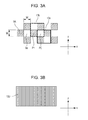
- FIGS. 3A and 3B illustrate a relationship between the pattern of the light transmitting regions 9 a and the light shielding regions 9 A and the grating 12 d directly below the light transmitting regions 9 a and the light shielding regions 9 A.
- FIG. 3A is a plan view illustrating the pattern of the light transmitting regions 9 a and the light shielding regions 9 A.
- FIG. 3B is a plan view illustrating the grating 12 d directly below the light transmitting regions 9 a and the light shielding regions 9 A.
- FIG. 3C is similar to FIG. 2A and illustrates a cross section that is parallel with the xz plane and illustrates a positional relationship among these members including the detectors. As illustrated in FIG.
- the grating 12 d has a uniform grating vector that coincides with the x-axis direction. Assume that a detection region directly below the light transmitting regions 9 a is P0 and that a detection region directly below the light shielding regions 9 A is P1, P0 and P1 form a checkered pattern having a size of W ⁇ W.
- a pixel region 13 a indicated by the solid line in FIG. 3A includes two detection regions P0 and two detection regions P1, and a pixel region 13 b indicated by the broken line in FIG. 3A also includes two detection regions P0 and two detection regions P1.
- each of the pixel regions always includes two detection regions P0 and two detection regions P1 although a positional relationship thereof may change.
- the detected light amounts are subjected to an interpolation process by calculating q0 and Q0 in the formula 1. If the resolution is determined by a pixel size, the resolution is 2 W ⁇ 2 W that is the size of the pixel regions 13 a and 13 b . However, the resolution after the interpolation process improves to W ⁇ W since the same interpolation process applies even if the pixels are moved by the width W in any direction within the xy plane.
- FIGS. 4A through 4H illustrate how 1-pulse-oscillated incident light passes through the light coupling layer 12 and is then received by the light detector 10 .
- FIG. 4A is the same cross-sectional view as FIG. 2A .
- FIGS. 4B through 4H illustrate, in chronological order, results of electromagnetic analysis of a light intensity distribution using a finite-difference time-domain (FDTD) and are drawn corresponding to FIG. 4A .
- FDTD finite-difference time-domain
- the width W of each of the light transmitting regions 9 a and the light shielding regions 9 A in the x direction is 5.6 ⁇ m
- the pitch of the grating is 0.46 ⁇ m
- the depth of the grating in the z direction is 0.2 ⁇ m
- the high-refractive-index transparent layer (the second transparent layer) is a Ta 2 O 5 film
- the thickness t1 of the high-refractive-index transparent layer in the z direction is 0.34 ⁇ m
- the low-refractive-index transparent layer (the first transparent layer) is a SiO 2 film
- the thickness t2 of the low-refractive-index transparent layer in the z direction is 0.22 ⁇ m.
- the S-polarized light 6 a having a wavelength ⁇ 0 of 850 nm that has been pulse-oscillated so that a half width is 11 fs (3.3 ⁇ m when converted into a propagation distance) passes through the light transmitting regions 9 a .
- FIG. 4C oscillation of the light 6 a ends, and the guided light 6 b and 6 c that propagates in the stacked high-refractive-index transparent layers 12 b is generated, and a component that has not become guided light passes through the light coupling layer 12 as it is and enters the microlens 11 a as the light 6 d .
- FIG. 4C the S-polarized light 6 a having a wavelength ⁇ 0 of 850 nm that has been pulse-oscillated so that a half width is 11 fs (3.3 ⁇ m when converted into a propagation distance) passes through the light transmitting regions 9 a .
- FIG. 4C oscillation of the light 6 a ends, and the guided light 6
- the guided light 6 b and 6 c propagates to a region below the light shielding regions 9 A while radiating the light 6 B 1 and 6 C 1 upward and downward.
- the transmitted light 6 d is collected onto the detector 10 a by the microlens 11 a .
- the transmitted light 6 d enters the detector 10 a .
- the radiated light 6 B 1 and 6 C 1 and the reflected light 6 B 2 form the radiated light 6 D and enter the microlens 11 A and are thus collected.
- the transmitted light 6 d and the radiated light 6 D are collected and enter the detectors 10 a and 10 A, respectively.
- the guided light 6 b and 6 c is not fully radiated in a range below the light shielding regions 9 A and part thereof reaches a range of an adjacent right-side light transmitting region in a state of guided light. Since a radiation loss coefficient (easiness of radiation of guided light) becomes larger as the depth of a grating becomes deeper, the amount of radiated light and the amount of detected light can be made larger as the depth of the grating in a region below the light shielding region 9 A is made deeper.
- FIG. 5A is a cross-sectional view illustrating a positional relationship between light that enters the four light transmitting regions 9 a and three detectors 10 a , 10 A, and 10 a ′ located below the light transmitting regions 9 a according to the examined example.
- t is a time
- r1, r2, r3, and r4 are random functions (functions having random values between 0 and 1)
- a is a random rate (the amplitude of the random values).
- FIG. 5B illustrates a result of analysis of a relationship between a random rate of incident light and a detection signal.
- a detector directly below the light shielding region 9 A located between central two of the four light transmitting regions 9 a is 10 A
- detectors directly below the two light transmitting regions 9 a adjacent to the detector 10 A are 10 a and 10 a ′
- light amounts detected by the detectors 10 A, 10 a , and 10 a ′ are P1, P0, and P0′, respectively
- the detection signal is defined as 2P1/(P0+P0′).
- the diamond shape, the square shape, and the triangle shape indicate analysis results obtained under conditions: TE mode incidence (S polarization), TM mode incidence (P polarization), and TEM mode incidence (random polarization, circular polarization, or polarization at 45 degrees), respectively.
- S polarization TE mode incidence
- P polarization TM mode incidence
- TEM mode incidence random polarization, circular polarization, or polarization at 45 degrees
- the detection signal decreases as the rate a increases.
- the degree of coherence (randomness of the phases) of the incident light can be found from the results illustrated in FIG. 5B on the basis of the value of the detection signal 2P1/(P0+P0′).
- the detection signal is correlated with a phase difference (not illustrated in FIG. 5B ), and therefore the phase difference can also be measured on the basis of the detection signal.
- a phase difference not illustrated in FIG. 5B
- 2P1/(P0+P0′) is used as the detection signal, but another signal may be used as the detection signal.
- the arithmetic circuit 14 may output, as the detection signal, at least one of (1) a signal indicative of a ratio P1/P0 of a second light amount P1 to a first light amount P0, (2) a signal indicative of a ratio P0/(P0+P1) of the first light amount P0 to the sum of the first light amount P0 and the second light amount P1, and (3) a signal indicative of a ratio P1/(P0+P1) of the second light amount P1 to the sum of the first light amount P0 and the second light amount P1 where the first light amount P0 is a light amount detected by the detector that faces the light transmitting region 9 a and the second light amount P1 is a light amount detected by the detector 10 A that faces the light shielding region 9 A.
- Each of these detection signals is correlated with the random rate a, and therefore the degree of coherent of the incident light can be found on the basis of the detection signal.
- FIG. 6 illustrates an example of wave trains that enter one of the light transmitting regions 9 a illustrated in FIG. 5A . Since the light source 2 emits light of a constant coherence length ⁇ 0, all of wave trains 15 a and 15 b that enter the light transmitting region 9 a have the same coherence length ⁇ 0 assuming that the coherence length does not change in the subject 4 . However, the wave trains 15 a and 15 b enter the light transmitting region 9 a at different timings due to scattering. A wave train that has the same coherence length ⁇ 0 and has a different phase follow the wave trains 15 a and 15 b . As illustrated in FIG.
- the wave trains 15 a and 15 b interfere with each other to form three wave trains 15 A, 15 B, and 15 C.
- the wave train 15 C is a wave train that is generated by overlapping and interference between the wave trains 15 a and 15 b .
- the wave trains 15 A and 15 B are remaining parts of the wave train 15 a and the wave train 15 b that do not overlap each other.
- the wave trains 15 A, 15 B, and 15 C have the same wavelength, and the expanse of wavelength (longitudinal mode width) of the composite wave (the wave trains 15 A, 15 B, and 15 C) is the same as that of the original wave trains 15 a and 15 b . That is, a coherence length defined by time coherence does not change (see FIGS. 13A through 13E ). However, there is no correlation in phase among the wave trains 15 A, 15 B, and 15 C, and continuity of the waves, i.e., the length of waves having a continuous phase is effectively shorter than the original length ⁇ 0.
- FIG. 7A illustrates overall optical arrangement and light beam tracing in the analysis.
- FIGS. 7B through 7D illustrates a result of analysis of an image 8 b at a detection position that is divided into 20 ⁇ 20 regions.
- FIG. 7B illustrates a light intensity distribution
- FIG. 7C illustrates an optical path length average distribution
- FIG. 7 D illustrates an optical path length standard deviation distribution.
- the human head includes a scalp 4 a , a skull 4 b , a cerebrospinal fluid (CFS) layer 4 c , a blood layer 4 e , and a gray matter 4 d .
- CFS cerebrospinal fluid
- Table 1 illustrates absorption coefficients (1/mm), scattering coefficients (1/mm), anisotropic scattering parameters, and film thicknesses (mm) of the respective parts.
- the blood layer 4 e has an oxygenated hemoglobin layer and a reduced hemoglobin layer that are arranged in a direction normal to the paper on which FIG. 7A is drawn.
- a distribution of scattered light from this region is obtained by calculation.
- a whiter region has a higher intensity.
- FIGS. 7C and 7D a whiter region has a larger value.
- a region of y>0 corresponds to the oxygenated hemoglobin layer, and a region of y ⁇ 0 corresponds to the reduced hemoglobin layer.
- FIGS. 7B through 7D there is a slight difference between the oxygenated hemoglobin layer and the reduced hemoglobin layer. Since an image inverted by the light collecting lens 7 is obtained, the positions of the oxygenated hemoglobin layer and the reduced hemoglobin layer in the image are reverse to actual positions.
- the light source 2 oscillates light having a coherence length of ⁇ 0.
- a standard deviation of an optical path length is equal to or smaller than the coherence length ⁇ 0, it is likely that received light is within the same wave train, and correlation of phases is high. In this case, the received light appears as a mixture of bright and dark parts.
- the standard deviation of the optical path length is equal to or larger than ⁇ 0, it is likely that wave trains of the received light are different, and there is no correlation of phases (see FIG. 12 ). In this case, the received light has uniform brightness at any position. As described with reference to FIG.
- the degree of coherence of incident light is related, for example, to the detection signal 2P1/(P0+P0′), P1/P0, or P1/(P0+P1). It is therefore possible to determine whether or not the standard deviation of incident light is equal to or larger than the coherence length ⁇ 0 on the basis of the value of the detection signal.
- FIGS. 7E and 7F illustrate an example of a distribution of a detection signal (P1/P0 in this example).
- the black regions in FIGS. 7E and 7F represent regions where the detection signal is uniformly small.
- the detection signal is small in regions (black regions) in which the standard deviation of the optical path length exceeds 18.5 mm.
- the detection signal is small in regions (black regions) in which the standard deviation of the optical path length exceeds 18.0 mm.
- the regions (black regions) in which the detection signal is small are wider than those in the example of FIG. 7E .
- places in which the detection signal is large and places in which the detection signal is small are mixed in a narrow range, and the value of the detection signal irregularly changes depending on the position. It is possible to know scattering in a subject by analyzing the black regions while using the coherence length ⁇ 0 as a parameter.
- the control circuit 1 controls the light source 2 , the light detection device 13 , and the arithmetic circuit 14 so that the coherence length of light emitted from the light source 2 is changed and an image is taken for each changed coherence length.
- the arithmetic circuit 14 generates and outputs, for each coherence length of light changed by the control circuit 1 , for example, at least one of (1) a signal indicative of a ratio P1/P0 of the second light amount P1 to the first light amount P0, (2) a signal indicative of a ratio P0/(P0+P1) of the first light amount P0 to the sum of the first light amount P0 and the second light amount P1, and (3) a signal indicative of a ratio P1/(P0+P1) of the second light amount P1 to the sum of the first light amount P0 and the second light amount P1. It is possible to know scattering in the subject on the basis of these signals.
- light sources such as a high-frequency superimposing semiconductor laser and a sweep light source (a light source that periodically sweeps a laser wavelength in a range of several nm to several tens of nm) have been put into practice.
- a semiconductor laser driven by a high-frequency superimposing circuit in general, a frequency of 300 MHz oscillates in a coherence length ranging from 0.1 mm to 0.2 mm and can make the coherence length variable within a range from 0.2 mm to several tens of mm by changing the frequency, amplitude, or the like of the superimposing circuit (e.g., reducing the frequency).
- a coherence length can be made variable within a range from 0.3 mm to several tens of mm by changing a wavelength fluctuation width or a cycle (frequency).
- the bandpass filter 9 p is used in some cases to limit a wavelength of light that enters the light coupling layer 12 .
- a desired coherence length can be obtained by combining a light source having a wide line width such as an LED and a bandpass filter having a narrow bandwidth.
- two or more light sources having different wavelengths may be used.
- a coherence length becomes short according to a wavelength difference of light from the two light sources.
- this may be associated with an operation of changing a light emission intensity ratio of the light sources.
- a distribution difference between oxygenated hemoglobin and reduced hemoglobin 4 e inside the skull 4 b of the subject illustrated in FIG. 7A can be detected as an output difference of an electric signal.
- This does not require time division and therefore makes it possible to markedly simplify measurement as compared with a method (second conventional example) for detecting an optical intensity distribution image described with reference to FIGS. 14A and 14B .
- it is possible to compare and analyze scattering in a subject just by changing the coherence length of the light source 2 and increase the resolution of measurement.
- the light detection device of the examined example has a room for improvement in terms of resolution.
- the width W of the light transmitting regions 9 a and the light shielding regions 9 A in the x direction is sufficiently large. More specifically, the width W need be approximately 10 times the pitch (i.e., period) A of the grating. This restricts the resolution after the interpolation process to the width W even if the interpolation process described with reference to FIGS. 3A and 3B is used.
- a light detection device includes a polarizer array having a region (light transmitting region) that transmits incident light polarized in one direction and a region (light shielding region) that blocks the incident light.
- the light transmitting region faces some of the plurality of detectors, and the light shielding region faces the others of the plurality of detectors.
- the azimuth of a grating in the light transmitting region is orthogonal to that in the light shielding region. According to such a configuration, it is possible to acquire two kinds (S polarization and P polarization) of scattering information and to increase the resolution of detection.
- light detectors are disposed within the reach of light (evanescent component) oozing out from light propagating in a light coupling layer. This makes it easy to detect the light propagating in the light coupling layer.
- a light detection device includes a polarizer array having a region (light transmitting region) that transmits incident light polarized in one direction and a region (light shielding region) that blocks the incident light.
- the light transmitting region faces some of the plurality of detectors, and the light shielding region faces the others of the plurality of detectors.
- the pitch of a grating in the light transmitting region is different from that in the light shielding region. According to such a configuration, it is possible to acquire two kinds (S polarization and P polarization) of scattering information and to increase the resolution of detection.
- a light detection device is configured such that each polarizer included in the polarizer array is made up of a plurality of linear metal wires that are periodically disposed at certain intervals. Since the azimuth of the metal wires in the light transmitting region is orthogonal to that in the light shielding region, optical separation based on polarization is possible.
- a light detection device is configured such that a linear polarizer that causes incident light to be polarized uniformly in one direction is disposed on the polarizer array.
- the polarization azimuth of the incident light changes in accordance with rotation of the linear polarizer about a normal to the surface. This makes it possible to easily exchange the positions of the light transmitting region and the light shielding region.
- the present disclosure includes a light detection device and a light detection system described in the following items.
- a light detection device includes:
- a light detector that has a main surface and includes a first detector and a second detector that are both disposed along the main surface;
- the light coupling layer disposed on or above the light detector, the light coupling layer including
- a polarizer array that is disposed on the light coupling layer and includes a first polarizer that transmits light polarized in one direction and a second polarizer that is adjacent to the first polarizer and blocks the light polarized in the one direction, wherein:
- the first grating and the first polarizer face the first detector
- the second grating and the second polarizer face the second detector.
- the light detection device may be configured such that
- the first detector is disposed within reach of an evanescent component of first light that passes through the second polarizer and propagates in the light coupling layer;
- the second detector is disposed within reach of an evanescent component of second light that passes through the first polarizer and propagates in the light coupling layer.
- the light detection device according to Item 2 may be configured such that, in operation,
- the first detector detects light that has passed through the first polarizer and the evanescent component of the first light at a first time
- the second detector detects light that has passed through the second polarizer and the evanescent component of the second light at a second time different from the first time.
- the light detection device may be configured such that
- the first polarizer and the second polarizer each include linear metal wires that are periodically disposed at certain intervals;
- a direction in which the metal wires of the first polarizer extend is orthogonal to a direction in which the metal wires of the second polarizer extend.
- the light detection device may further include:
- a linear polarizer that is disposed on or above the polarizer array and causes light entering the polarizer array to be polarized in a specific direction;
- a first control circuit that, in operation, controls the motor.
- the light detection device may be configured such that, in operation,
- the first control circuit causes the light detector to perform light detection for a first time in a state where a direction of a polarized light transmission axis of the linear polarizer is same as a direction of a polarized light transmission axis of the first polarizer by controlling the motor;
- the first control circuit causes the light detector to perform light detection for a second time in a state where the direction of the polarized light transmission axis of the linear polarizer is same as a direction of a polarized light transmission axis of the second polarizer by controlling the motor.
- the light detection device may be configured such that
- the light coupling layer further includes
- the second high-refractive-index layer has a higher refractive index than the first low-refractive-index layer and the third low-refractive-index layer;
- the third grating faces the first detector
- the fourth grating faces the second detector.
- a light detection system includes:
- the arithmetic circuit in operation, outputting at least one signal selected from the group consisting of (1) a signal indicating a ratio of a second light amount to a first light amount, (2) a signal indicating a ratio of the first light amount to a sum of the first light amount and the second light amount, and (3) a signal indicating a ratio of the second light amount to the sum, the first light amount being a light amount detected by the first detector and the second light amount being a light amount detected by the second detector.
- the light detection system according to Item 8 may be configured such that
- a plurality of first detectors are provided in the light detector, each of the plurality of first detectors being the first detector;
- each of the plurality of second detectors being the second detector
- a plurality of first gratings are provided in the first high-refractive-index layer, each of the plurality of first gratings being the first grating;
- a plurality of second gratings are provided in the first high-refractive-index layer, each of the plurality of second gratings being the second grating;
- a plurality of first polarizers are provided in the polarizer array, each of the plurality of first polarizers being the first polarizer;
- a plurality of second polarizers are provided in the polarizer array, each of the plurality of second polarizers being the second polarizer;
- the plurality of first polarizers and the plurality of second polarizers include pairs of adjacent first and second polarizers
- the arithmetic circuit in operation, outputs the at least one signal for each of the pairs.
- the light detection system according to Item 9 may be configured such that
- the arithmetic circuit in operation, generates image information representing a pair in which a value of the at least one signal is equal to or larger than a threshold value and a pair in which the value of the at least one signal is smaller than the threshold value.
- the light detection system according to any one of Items 8 through 10 may further include
- a light source that, in operation, emits light of a wavelength band
- the light detection device further includes a bandpass filter that is disposed on or above the light coupling layer and selectively transmits the light of the wavelength band.
- the light detection system according to any one of Items 8 through 10 may further include:
- the second control circuit in operation, changing a coherence length of light emitted from the light source.
- the light detection system according to Item 12 may be configured such that
- the arithmetic circuit in operation, outputs the at least one signal for each coherence length of light changed by the second control circuit.
- a light detection device includes:
- a light detector that has a main surface and includes a first detector and a second detector that are both disposed along the main surface;
- the light coupling layer disposed on or above the light detector, the light coupling layer including
- a polarizer array that is disposed on the light coupling layer and includes a first polarizer that transmits light polarized in one direction and a second polarizer that is adjacent to the first polarizer and blocks the light polarized in the one direction, wherein:
- the first grating and the first polarizer face the first detector
- the second grating and the second polarizer face the second detector
- a period of the first grating is different from that of the second grating.
- the light detection device according to Item 14 may be configured such that
- the first polarizer and the second polarizer each includes linear metal wires that are periodically disposed at certain intervals; and a direction in which the metal wires of the first polarizer extend is orthogonal to a direction in which the metal wires of the second polarizer extend.
- the light detection device may further include:
- a linear polarizer that is disposed on or above the polarizer array and causes light entering the polarizer array to be polarized in a specific direction;
- a first control circuit that, in operation, controls the motor.
- the light detection device according to Item 16 may be configured such that, in operation,
- the first control circuit causes the light detector to perform light detection for a first time in a state where a direction of a polarized light transmission axis of the linear polarizer is same as a direction of a polarized light transmission axis of the first polarizer by controlling the motor;
- the first control circuit causes the light detector to perform light detection for a second time in a state where the direction of the polarized light transmission axis of the linear polarizer is same as a direction of a polarized light transmission axis of the second polarizer by controlling the motor.
- the light detection device may be configured such that
- the light coupling layer further includes
- the second high-refractive-index layer has a higher refractive index than the first low-refractive-index layer and the third low-refractive-index layer;
- the third grating faces the first detector
- the fourth grating faces the second detector
- a direction of periodicity of the third grating being same as a direction of periodicity of the first grating
- a direction of periodicity of the fourth grating being same as a direction of periodicity of the second grating.
- a light detection system according to Item 19 of the present disclosure:
- the arithmetic circuit in operation, outputting at least one signal selected from the group consisting of (1) a signal indicating a ratio of a second light amount to a first light amount, (2) a signal indicating a ratio of the first light amount to a sum of the first light amount and the second light amount, and (3) a signal indicating a ratio of the second light amount to the sum, the first light amount being a light amount detected by the first detector and the second light amount being a light amount detected by the second detector.
- the light detection system according to Item 19 may be configured such that
- a plurality of first polarizers are provided in the polarizer array, each of the plurality of first polarizers being the first polarizer;
- a plurality of second polarizers are provided in the polarizer array, each of the plurality of second polarizers being the second polarizer;
- the plurality of first polarizers and the plurality of second polarizers include pairs of adjacent first and second polarizers
- the arithmetic circuit outputs the at least one signal for each of the pairs.
- the light detection system according to Item 20 may be configured such that
- the arithmetic circuit in operation, generates image information representative of a pair in which a value of the at least one signal is equal to or larger than a threshold value and a pair in which the value of the at least one signal is smaller than the threshold value.
- the light detection system according to any one of Items 19 through 21 may further include
- a light source that, in operation, emits light of a wavelength band
- the light detection device further includes a bandpass filter that is disposed on or above the light coupling layer and selectively transmits the light of the wavelength band.
- the light detection system according to any one of Items 19 through 21 may further include:
- the second control circuit in operation, changing a coherence length of light emitted from the light source.
- the light detection system according to Item 23 may be configured such that
- the arithmetic circuit in operation, outputs the at least one signal for each coherence length of light changed by the second control circuit.
- any of circuit, unit, device, part or portion, or any of functional blocks in the block diagrams may be implemented as one or more of electronic circuits including, but not limited to, a semiconductor device, a semiconductor integrated circuit (IC) or a large scale integration (LSI).
- the LSI or IC can be integrated into one chip, or also can be a combination of plural chips.
- functional blocks other than a memory may be integrated into one chip.
- the name used here is LSI or IC, but it may also be called system LSI, very large scale integration (VLSI), or ultra large scale integration (ULSI) depending on the degree of integration.
- a Field Programmable Gate Array (FPGA) that can be programmed after manufacturing an LSI or a reconfigurable logic device that allows reconfiguration of the connection or setup of circuit cells inside the LSI can be used for the same purpose.
- the software is recorded on one or more non-transitory recording media such as a ROM, an optical disk or a hard disk drive, and when the software is executed by a processor, the software causes the processor together with peripheral devices to execute the functions specified in the software.
- a system or apparatus may include such one or more non-transitory recording media on which the software is recorded and a processor together with necessary hardware devices such as an interface.
- the configuration of the present embodiment is the same as that of the examined example except for that an analyzer (linear polarizer) is disposed in front of a light detection device 13 and except for structures of light transmitting regions and light shielding regions, patterning of a grating, and positions of light detectors.
- an analyzer linear polarizer
- Constituent elements that are identical to those in the examined example are given identical reference signs, and overlapping description thereof is omitted.
- FIG. 8A is a plan view illustrating the way in which S-wave light transmitting regions 9 S, which correspond to first polarizers, and P-wave light transmitting regions 9 P, which correspond to second polarizers, are arranged in the present embodiment.
- a polarizer array including the S-wave light transmitting regions 9 S and the P-wave light transmitting regions 9 P, which are wire grid (metal grid) polarizers, is used instead of the light shielding film 9 of the examined example.
- a wire grid such as aluminum (Al) is provided at a pitch equal to or smaller than 1/3 of the wavelength along a direction of oscillation of an electric field of P-waves (the x-axis direction in FIG. 8A ). Since the metal wires extend in the x-axis direction, an electric current flows in this direction, and energy having an electric field vector in the x-axis direction is consumed. As a result, the S-wave light transmitting regions 9 S transmit only S-wave light and block P-wave light.
- metal grid such as aluminum (Al)
- a wire grid such as Al is provided at a pitch equal to or smaller than 1/3 of the wavelength along a direction of oscillation of an electric field of S-waves (the y-axis direction in FIG. 8A ). Since the metal wires extend in the y-axis direction, an electric current flows in this direction, and energy having an electric field vector in the y-axis direction is consumed. As a result, the P-wave light transmitting regions 9 P transmit only P-wave light and block S-wave light.
- the S-wave light transmitting regions 9 S which block P-waves, can be called “P-wave light shielding regions”.
- the P-wave light transmitting regions 9 P which block S-waves, can be called “S-wave light shielding regions”.
- S-wave and P-wave as used herein are defined on the basis of an incident surface that is parallel with an xz plane. Specifically, S-waves are linearly-polarized light having an electric field oscillating in a direction perpendicular to the incident surface, and P-waves are linearly-polarized light having an electric field oscillating in a direction parallel with the incident surface.
- FIG. 8B is a plan view illustrating azimuths of gratings provided in a light coupling layer 12 .
- FIGS. 8C and 8D are cross-sectional views each illustrating a positional relationship among constituent elements including light detectors 10 .
- FIG. 8C illustrates a cross section of the light detection device 13 that is parallel with the xz plane.
- FIG. 8D illustrates a cross section of the light detection device 13 that is parallel with the yz plane.
- a first grating 12 S is located directly below each of the S-wave light transmitting regions 9 S and has a grating vector in the x-axis direction.
- a second grating 12 P is located directly below each of the P-wave light transmitting regions 9 P and has a grating vector in the y-axis direction.
- part of S-wave light that has passed through the S-wave light transmitting regions 9 S is turned into TE mode guided light 6 b and 6 c propagating in the light coupling layer 12 in the x-axis direction by the first grating 12 S.
- a component of the light that has not been turned into guided light is detected by a first detector 10 S as transmitted light 6 d passing through the light coupling layer 12 .
- a light component that is finally radiated after being guided can be added to light entering the first detector 10 S, but this component is also characterized as a component that has not been turned into guided light in the present disclosure.
- the guided light 6 b and 6 c propagates in the light coupling layer 12 . Since a plurality of layers in the light coupling layer 12 are stacked close to one another, guided light propagates while moving between the layers of the light coupling layer 12 and enters the region of the second grating 12 P. In the region of the second grating 12 P, the azimuth (y-direction) of the grating vector of the second grating 12 P is orthogonal to the propagation direction of the guided light 6 b and 6 c , and therefore the guided light 6 b and 6 c is not radiated from the light coupling layer 12 .
- the first detector 10 S is disposed within the reach of an evanescent component of light that passes through the P-wave light transmitting region 9 P, which is a second polarizer, and propagates in the light coupling layer 12
- the second detector 10 P is disposed within the reach of an evanescent component of light that passes through the S-wave light transmitting region 9 S, which is a first polarizer, and propagates in the light coupling layer 12 .
- the first detector 10 S and the second detector 10 P are disposed close to the light coupling layer 12 , and a guided component (evanescent light) oozing out from the light coupling layer 12 is guided toward the second detector 10 P side (leaky mode light 6 D).
- a high-refractive-index protection layer 10 e is provided on surfaces of the light detectors 10 , but the protection layer 10 e may be omitted.
- P-wave light that has passed through the P-wave light transmitting region 9 P is turned into TE mode guided light 6 B and 6 C propagating in the light coupling layer 12 in the y-axis direction by the second grating 12 P.
- a component that has not been turned into guided light passes through the light coupling layer 12 (transmitted light 6 D) and is then detected by the second detector 10 P.
- the guided light 6 B and 6 C propagates in the light coupling layer 12 . Since a plurality of layers in the light coupling layer 12 are stacked close to one another, the guided light propagates while moving between the layers of the light coupling layer 12 and enters the region of the first grating 12 S.
- the azimuth (x-direction) of the grating vector of the first grating 12 S is orthogonal to the propagation direction of the guided light 6 B and 6 C, and therefore the guided light 6 B and 6 C is not radiated from the light coupling layer 12 .
- the first detector 10 S and the second detector 10 P are disposed close to the light coupling layer 12 , and a guided component (evanescent light) oozing out from the light coupling layer 12 is guided toward the first detector 10 S side (leaky mode light 6 d ). In this way, the guided light 6 B and 6 C can be detected by the first detector 10 S.
- a detection region A0 directly below the S-wave light transmitting region 9 S and a detection region A1 directly below the P-wave light transmitting region 9 P form a checkered pattern having a size of W ⁇ W.
- the detected light amounts are subjected to an interpolation process by calculating q0 and Q0 in the formula 1. If the resolution is determined by a pixel size, the resolution is 2 W ⁇ 2 W that is the size of the pixel regions 13 a and 13 b . However, the resolution after the interpolation process improves to W ⁇ W since the same interpolation process applies even if the pixels are moved by the width W in any direction within the xy plane.
- a polarization direction of the light 5 that enters the light transmitting regions 9 a illustrated in FIG. 1B (corresponding to the S-wave light transmitting regions 9 S and the P-wave light transmitting regions 9 P illustrated in FIG. 8A ) is random.
- an analyzer 16 which is a linear polarizer, is provided in front of (on a subject side) of a transparent substrate 9 b .
- the analyzer 16 transmits only specific linearly-polarized light of the incident light 5 .
- the analyzer 16 is connected to a motor (not illustrated) and rotates about a central axis extending in the z direction. This makes it possible to select a polarization azimuth. In the state illustrated in FIG.
- the guided light 6 b , 6 c , 6 B, 6 C is TE mode guided light.
- the guided light 6 b , 6 c , 6 B, 6 C may be TM mode guided light by changing the pitch of the first grating 12 S and the second grating 12 P.
- the configuration of the present embodiment may be combined with a time-division detection method (second conventional example) described with reference to FIGS. 14A and 14B . This makes it possible to analyze a signal that is taken in in a time-division manner in a coherence state. It is therefore possible to analyze scattering in a subject in more detail.
- FIG. 9 is a diagram schematically illustrating the configuration of the light detection device 13 according to the present embodiment.
- FIG. 9 illustrates a motor 15 and a control circuit 1 ′ in addition to the constituent elements of the light detection device 13 illustrated in FIG. 8C .
- the analyzer 16 illustrated in FIG. 9 is actually disposed so as to entirely cover the plurality of S-wave light transmitting regions 9 S and the plurality of P-wave light transmitting regions 9 P.
- the light detection device 13 includes light detectors 10 including the first detector 10 S and the second detector 10 P disposed along a main surface (imaging surface), the light coupling layer 12 disposed on or above the light detector 10 , and a polarizer array 9 ′ disposed on or above the light coupling layer 12 .
- the expression “on or above” means that one element is located on an upper side of another element based on the arrangement illustrated in the drawings of the present disclosure and encompasses a state where one element is located on an upper side of another element in contact with the other element and a state where one element is located on an upper side of another element without contact with the other element (i.e., with another element or layer interposed therebetween).
- the light coupling layer 12 includes a first low-refractive-index layer 12 c , a first high-refractive-index layer 12 b that is disposed on the first low-refractive-index layer 12 c and includes the first grating 12 S and the second grating 12 P, and a second low-refractive-index layer 12 a disposed on the first high-refractive-index layer 12 b , as in FIG. 2A .
- the first high-refractive-index layer 12 b has a higher refractive index than the first low-refractive-index layer 12 c and the second low-refractive-index layer 12 a .
- the light coupling layer 12 further includes a third low-refractive-index layer disposed between the first low-refractive-index layer 12 c and the light detector 10 and a second high-refractive-index layer that is disposed between the third low-refractive-index layer and the first low-refractive-index layer 12 c and includes a third grating and a fourth grating.
- the second high-refractive-index layer has a higher refractive index than the first low-refractive-index layer 12 c and the third low-refractive-index layer.
- a direction of periodicity of the third grating is the same as that of the first grating.
- a direction of grooves of the third grating is also the y direction
- a direction of grooves of the third grating is also the x direction
- a direction of periodicity of the fourth grating is the same as that of the second grating.
- the light coupling layer 12 has a plurality of combinations of two low-refractive-index layers and a high-refractive-index layer sandwiched therebetween and having gratings in addition to the aforementioned one.
- the light coupling layer 12 functions as an optical waveguide due to such a structure in which gratings are stacked. Note that the number of combinations of two low-refractive-index layers and a high-refractive-index layer sandwiched therebetween and having gratings is not limited in particular, and it is only necessary that at least one combination be provided.
- the polarizer array 9 ′ includes the S-wave light transmitting region 9 S, which is a first polarizer that transmits light polarized in one direction, and the P-wave light transmitting region 9 P, which is a second polarizer that is adjacent to the S-wave light transmitting region and blocks the light polarized in the one direction. At least one combination of the S-wave light transmitting region 9 S and the P-wave light transmitting region 9 P suffices to perform arithmetic processing described in the examined example.
- a bandpass filter that selectively transmits light of a wavelength band emitted by the light source 2 may be provided on the light coupling layer 12 (not illustrated in FIG. 9 ), as in the configuration illustrated in FIG. 2A .
- a single S-wave light transmitting region 9 S faces a single first detector 10 S
- a single P-wave light transmitting region 9 P faces a single second detector 10 P.
- the present embodiment is not limited to such a configuration. It is also possible to employ a configuration in which a single S-wave light transmitting region 9 S faces two or more first detectors 10 S that are close to one another, and a single P-wave light transmitting region 9 P faces two or more second detectors 10 P that are close to one another.
- the computation described in the examined example can be applied as it is in a case where the arithmetic circuit 14 ( FIG. 1A ) processes, as a single signal, each of the sum of signals from the two or more first detectors 10 S and the sum of signals from the two or more second detectors 10 P.
- a direction of periodicity of the first grating that faces the S-wave light transmitting region 9 S is orthogonal to that of the second grating that faces the P-wave light transmitting region 9 P, unlike the examined example.
- the first detector 10 S detects light that has passed through the S-wave light transmitting region 9 S and an evanescent component of light that passes through the P-wave light transmitting region 9 P and propagates in the light coupling layer 12 .
- the second detector 10 P detects light that has passed through the P-wave light transmitting region 9 P and an evanescent component of light that passes through the S-wave light transmitting region 9 S and propagates in the light coupling layer 12 .
- the light detection device 13 includes the analyzer 16 , which is a linear polarizer that is disposed on the polarizer array 9 ′ and causes light entering the polarizer array 9 ′ to be polarized uniformly in a specific direction, a motor 15 that rotates the analyzer 16 about an axis perpendicular to the main surface (imaging surface) of the light detector 10 , and a first control circuit 1 ′ that controls the motor 15 and the light detector 10 .
- the first control circuit 1 ′ may be the same as or may be different from the control circuit 1 (second control circuit) illustrated in FIG. 1A .
- the first control circuit 1 ′ causes the light detector 10 to perform light detection for the first time in a state where a direction of a polarized light transmission axis of the analyzer 16 is the same as that of the S-wave light transmitting region 9 S.
- the first control circuit 1 ′ causes the light detector 10 to perform light detection for the second time in a state where the direction of the polarized light transmission axis of the analyzer 16 is the same as that of the P-wave light transmitting region 9 P.
- the first detector 10 S and the second detector 10 P can acquire information of two kinds of polarized light having polarization directions orthogonal to each other. This substantially doubles the resolution as compared with the configuration of the examined example.
- the arithmetic circuit 14 performs processing similar to that in the examined example. Specifically, the arithmetic circuit 14 generates and outputs, for example, at least one signal selected from a group consisting of (1) a signal indicative of a ratio P1/P0 of a second light amount P1 to a first light amount P0, (2) a signal indicative of a ratio P0/(P0+P1) of the first light amount P0 to the sum of the first light amount P0 and the second light amount P1, and (3) a signal indicative of a ratio P1/(P0+P1) of the second light amount P1 to the sum of the first light amount P0 and the second light amount P1 where the first light amount P0 is a light amount detected by the first detector 10 S that faces the S-wave light transmitting region 9 S and the second light amount P1 is a light amount detected by the second detector 10 P that faces the P-wave light transmitting region 9 P.
- This arithmetic processing can be performed for each pair of adjacent S-wave and P-wave light transmitting regions.
- information on a target can be acquired on the basis of any of the detection signals.
- the arithmetic circuit 14 finds the degree of coherence from the detection signal by referring to a function or a table that is stored in advance in a storage medium such as a memory and that defines a relationship between the detection signal and the degree of coherence (e.g., a random rate) (see FIG. 5B ).
- the arithmetic circuit 14 performs such generation of a signal and estimation of a structure of a target, for example, for each pair of adjacent S-wave and P-wave light transmitting regions. This makes it possible to obtain information on the target over a wide region.
- the arithmetic circuit 14 may generate any of the aforementioned detection signals for each coherence length of light changed by the control circuit 1 . This makes it possible to know details of scattering in a subject while using a coherence length as a parameter, as described with reference to FIGS. 7E and 7F .
- the arithmetic circuit 14 may generate image information in which a region where a value of a generated signal is equal to or larger than a predetermined threshold value and a region where the value of the signal is less than the threshold value are distinguished from each other, for example, as illustrated in FIGS. 7E and 7F . This can visualize an inner structure of the subject.
- a configuration of a light detection device is the same as that of Embodiment 1 except for patterning of gratings. Constituent elements that are identical to those in Embodiment 1 are given identical reference signs, and overlapping description thereof is omitted.
- FIG. 10A is a plan view illustrating arrangement of S-wave light transmitting regions 9 S and P-wave light transmitting regions 9 P in the present embodiment.
- a wire grid metal grid
- a wire grid such as Al is provided at a pitch equal to or smaller than 1/3 of the wavelength along a direction of oscillation of P-waves (x-axis direction). This allows the S-wave light transmitting region 9 S to transmit S-wave light and block P-wave light.
- a wire grid such as Al is provided at a pitch equal to or smaller than 1/3 of the wavelength along a direction of oscillation of S-waves (y-axis direction).
- the P-wave light transmitting region 9 P can transmit P-wave light and block S-wave light. Accordingly, the S-wave light transmitting region 9 S can be called a P-wave light shielding region, and the P-wave light transmitting region 9 P can be called an S-wave light shielding region.
- FIG. 10B is a plan view illustrating azimuths of gratings in a light coupling layer 12 .
- FIG. 10C is an xz plane cross-sectional view illustrating a positional relationship among constituent elements including a light detector 10 .
- a first grating 12 S is located directly below the S-wave light transmitting region 9 S and has a grating vector in the x-axis direction.
- the second grating 12 P is located directly below the P-wave light transmitting region 9 P, which is an S-wave light shielding region, and has a grating vector in the x-axis direction.
- the direction of the grating vector of the first grating 12 S that faces the S-wave light transmitting region 9 S is the same as that of the second grating 12 P that faces the P-wave light transmitting region 9 P, which is an S-wave light shielding region.
- the first grating 12 S and the second grating 12 P are different in terms of pitch (cycle).
- the pitch of the first grating 12 S satisfies a condition for excitation of TE mode guided light 6 b and 6 c .
- the pitch of the second grating 12 P satisfies a condition for excitation of TM mode guided light 6 B and 6 C.
- part of S-wave light that has passed through the S-wave light transmitting region 9 S is turned into TE mode guided light 6 b and 6 c propagating in the x-axis direction in the light coupling layer 12 by the first grating 12 S.
- a light component that has not been turned into guided light passes through the light coupling layer 12 (transmitted light 6 d ) and is then detected by the first detector 10 S.
- a light component that is finally radiated after being guided can be added to the light entering the first detector 10 S, but this component is also regarded as a component that has not been turned into guided light in the present disclosure.
- the guided light 6 b and 6 c propagates in the light coupling layer 12 . Since a plurality of layers in the light coupling layer 12 are stacked close to one another, guided light propagates while moving between the layers of the light coupling layer 12 and enters the region of the second grating 12 P. In the region of the second grating 12 P, light is radiated by the second grating 12 P, and the radiated light is detected by the second detector 10 P. Meanwhile, P-wave light that has passed through the P-wave light transmitting region 9 P is turned into TM mode guided light 6 B and 6 C propagating in the x-axis direction in the light coupling layer 12 by the second grating 12 P.
- a light component that has not been turned into guided light passes through the light coupling layer 12 (transmitted light 6 D) and is then detected by the second detector 10 P.
- the guided light 6 B and 6 C propagates in the light coupling layer 12 . Since a plurality of layers in the light coupling layer 12 are stacked close to one another, the guided light propagates while moving between the layers of the light coupling layer 12 . In the region of the first grating 12 S, light is radiated by the first grating 12 S, and the radiated light is detected by the first detector 10 S. In the present embodiment, since a radiation effect is anticipated by the gratings, it is unnecessary to dispose the first detector 10 S and the second detector 10 P close to the light coupling layer 12 , unlike Embodiment 1.
- the light detection device according to the present embodiment may include a microlens as in the examined example.
- a detection region A0 directly below the S-wave light transmitting region 9 S and a detection region A1 directly below the P-wave light transmitting region 9 P form a checkered pattern having a size of W ⁇ W.
- the detected light amounts are subjected to an interpolation process by calculating q0 and Q0 in the formula 1. If the resolution is determined by a pixel size, the resolution is 2 W ⁇ 2 W that is the size of the pixel regions 13 a and 13 b . However, the resolution after the interpolation process improves to W ⁇ W since the same interpolation process applies even if the pixels are moved by the width W in any direction within the xy plane.
- a polarization direction of the light 5 that enters the light transmitting region 9 a illustrated in FIG. 1B (corresponding to the S-wave light transmitting region 9 S and the P-wave light transmitting region 9 P illustrated in FIG. 10A ) is random.
- an analyzer 16 which is a linear polarizer, is provided in front of (on a subject side) of a transparent substrate 9 b .
- the analyzer 16 transmits only specific linearly-polarized light of the incident light 5 .
- the analyzer 16 is connected to a motor (not illustrated) and rotates about a central axis extending in the z direction. This makes it possible to select a polarization azimuth. In the configuration illustrated in FIG.
- the guided light 6 b and 6 c is TE mode guided light
- guided light 6 B and 6 C is TM mode guided light
- the guided light 6 b and 6 c may be TM mode guided light
- guided light 6 B and 6 C may be TE mode guided light by changing the pitch of the first grating 12 S and the pitch of the second grating 12 P.
- the configuration of the present embodiment may be combined with a time-division detection method (second conventional example) described with reference to FIGS. 14A and 14B . This makes it possible to analyze a signal that is taken in in a time-division manner in a coherence state. It is therefore possible to analyze scattering in a subject in more detail.
Landscapes
- Physics & Mathematics (AREA)
- General Physics & Mathematics (AREA)
- Spectroscopy & Molecular Physics (AREA)
- Optics & Photonics (AREA)
- Investigating Or Analysing Materials By Optical Means (AREA)
Abstract
A light detection device includes a light detector including a first detector and a second detector; a light coupling layer disposed on or above the light detector; and a polarizer array that is disposed on the light coupling layer. The light coupling layer includes a first low-refractive-index layer, a first high-refractive-index layer including a first grating and a second grating adjacent to the first grating, and a second low-refractive-index layer in this order. The polarizer array includes a first polarizer that transmits light polarized in one direction and a second polarizer that is adjacent to the first polarizer and blocks the light polarized in the one direction. The first grating and the first polarizer face the first detector, and the second grating and the second polarizer face the second detector.
Description
The present disclosure relates to a light detection device, a light detection system, a light detection method, and the like.
Light is an electromagnetic wave and is characterized not only by wavelength and intensity, but also by properties such as polarization and coherence. An example of a method for measuring a subject by utilizing coherence of light among these properties is a Michelson interferometer described in “Principles of Optics” (TOKAI UNIVERSITY PRESS, p. 482, M. Born, et al.).
In one general aspect, the techniques disclosed here feature a light detection device including: a light detector that has a main surface and includes a first detector and a second detector that are both disposed along the main surface; a light coupling layer disposed on or above the light detector; and a polarizer array disposed on the light coupling layer. The light coupling layer includes a first low-refractive-index layer, a first high-refractive-index layer that is disposed on the first low-refractive-index layer and includes a first grating and a second grating adjacent to the first grating, and a second low-refractive-index layer that is disposed on the first high-refractive-index layer. The first high-refractive-index layer has a higher refractive index than the first low-refractive-index layer and the second low-refractive-index layer. The polarizer array includes a first polarizer that transmits light polarized in one direction and a second polarizer that is adjacent to the first polarizer and blocks the light polarized in the one direction. The first grating and the first polarizer face the first detector, and the second grating and the second polarizer face the second detector.
It should be noted that general or specific embodiments may be implemented as a system, a method, an integrated circuit, a computer program, a storage medium, or any selective combination thereof.
Additional benefits and advantages of the disclosed embodiments will become apparent from the specification and drawings. The benefits and/or advantages may be individually obtained by the various embodiments and features of the specification and drawings, which need not all be provided in order to obtain one or more of such benefits and/or advantages.
A result of detailed study on a conventional method for measuring coherence or a phase of light is described below before description of the embodiments of the present disclosure.
The same principle holds even in a case where the reflection mirror 34A is fixed and a transparent subject 4 is displaced between the half mirror 33 and the reflection mirror 34 a. An intensity difference corresponding to the shape of a subject appears as a spatial distribution in the intensity of the signal detected by the light detector 36. That is, an interference pattern is formed. By measuring the shape or interval of the interference pattern, the shape (phase information) of the subject can be measured.
Next, a configuration similar to a light detection system disclosed in “Near-infrared Spectroscopy in a 1-μm Wavelength Region: Current and Future” (The 14th Annual Meeting of Japanese Society for Medical Near Infrared Spectroscopy, pp. 139-144, Goro NISHIMURA) is described as a second conventional example. The light detection system in the second conventional example measures a light intensity distribution at each light propagation distance. FIG. 14A is a schematic cross-sectional view of a light detection system 300 in the second conventional example. A light source 42 emits laser light. As illustrated in FIG. 14A , light 43 having a wavelength λ0 is emitted from the light source 42 toward a subject 44. As a result, scattered light 45 a, 45 b, and 45 c generated on a surface of the subject 44 or in the subject 44 is collected by a light collecting lens 47 and forms an image 48 b on an image formation plane of the light collecting lens 47. A substantial object (a collection of object points) 48 a corresponding to the image 48 b exists on an object side of the lens. A light detector 50 is disposed on the image formation plane. The light detector 50 is a collection of a plurality of pixels and detects the amount of incident light in each pixel. The light source 42 is connected to a controller 41, and light emission of the light source 42 is controlled by the controller 41. The amount of light detected by the light detector 50 is processed in an arithmetic circuit 51 as a detection signal. The controller 41 and the arithmetic circuit 51 are collectively controlled by a computer 52.
According to the study of the inventors of the present invention, reference light 32B and 32C from the reflection mirror 34A is needed to measure the degree of coherence or a phase of light by using the Michelson interferometer 200 that is the first conventional example. This complicates the configuration.
According to the study of the inventors of the present invention, the light detection system that is the second conventional example has a limitation on the width of a divided time. It is therefore impossible to sufficiently secure resolution in a depth direction in diagnosis. For example, in a case where the width of a divided time is 300 picoseconds (ps), the depth resolution is approximately 90 mm, and is not suitable for diagnosis and inspection of a relatively small target such as a biological object.
An aspect (examined example) examined to solve the problems of the conventional examples is described before description of the embodiments of the present disclosure.
The light source 2 irradiates a subject (target) 4 with light 3 having a constant coherence length σ0. The light source 2 emits, for example, laser light that is a representative of coherent light. The light source 2 emits light of a constant intensity, and the control circuit 1 controls light detection of the light detection device 13, arithmetic processing of the arithmetic circuit 14, the amount of light emission, an ON timing, a continuous ON period, or a light emission wavelength or a coherence length of the light source 2 by executing a program. The control circuit 1 can be, for example, an integrated circuit such as a central processing unit (CPU) or a microcomputer. The control circuit 1 and the arithmetic circuit 14 may be a unified single circuit.
The light detection system 100 may include, for example, a display on which a result of the arithmetic processing in the arithmetic circuit 14 is displayed in addition to the constituent elements illustrated in FIG. 1A .
The light detection device 13 has a plurality of light transmitting regions and a plurality of light shielding regions that face a plurality of detectors (sometimes referred to as “light detection cells”), as described later. Light incident from a subject passes through the light transmitting regions and is blocked by the light shielding regions. Light that has passed through a light transmitting region enters a detector that faces the light transmitting region.
As illustrated in FIG. 2A , the light detection device 13 includes a light detector 10, a light coupling layer 12, and the light shielding layer 9 in this order. In the example illustrated in FIG. 2A , these members are stacked in the z direction. Furthermore, in the example illustrated in FIG. 2A , the light detection device 13 includes, on the light shielding layer 9, a transparent substrate 9 b and a bandpass filter 9 p in this order. The bandpass filter 9 p selectively transmits light of a wavelength band emitted by the light source 2.
The light detector 10 includes a plurality of detectors (light detection cells) 10 a and 10A disposed in a two-dimensional manner in an in-plane direction (within the xy plane) of the light detector 10. The light detector 10 includes microlenses 11 a and 11A, a transparent film 10 c, metal films 10 d such as wires, and photosensitive parts made of Si, an organic film, or the like in this order from a light incident side. The photosensitive parts in gaps between the metal films 10 d correspond to the detectors 10 a and 10A. The detectors 10 a and 10A have detection sensitivity in the wavelength band of light emitted from the light source 2. Each of the plurality of microlenses 11 a and 11A is disposed so as to face one of the plurality of detectors 10 a and 10A. Light that is collected by the microlenses 11 a and 11A and enters the gaps between the metal films 10 d is detected by the detectors 10 a and 10A.
The light coupling layer 12 is disposed on the light detector 10 and includes a first transparent layer 12 c, a second transparent layer 12 b, and a third transparent layer 12 a in this order in a direction (the z-axis direction) perpendicular to a surface of the light detector 10. The first transparent layer 12 c and the third transparent layer 12 a are made of SiO2 or the like. The second transparent layer 12 b is made of Ta2O5 or the like. The second transparent layer 12 b has a higher refractive index than the first transparent layer 12 c and the third transparent layer 12 a. The first transparent layer 12 c, the second transparent layer 12 b, and the third transparent layer 12 a are hereinafter sometimes referred to as a first low-refractive-index layer, a first high-refractive-index layer, and a second low-refractive-index layer, respectively. The first transparent layer 12 c and the third transparent layer 12 a are hereinafter sometimes referred to as low-refractive-index transparent layers, and the second transparent layer 12 b is hereinafter sometimes referred to as a high-refractive-index transparent layer. In the present disclosure, the terms “low refractive index” and “high refractive index” merely indicate a relative refractive index value and does not limit an absolute refractive index value of the layer.
The light detection device 13 may have a structure in which the high-refractive-index transparent layer 12 b and the low-refractive-index transparent layer 12 c are alternated in this order. In the example of FIG. 2A , the light detection device 13 has a structure in which the high-refractive-index transparent layer 12 b and the low-refractive-index transparent layer 12 c are alternated six times in total. The high-refractive-index transparent layer 12 b is sandwiched between the low-refractive-index transparent layers 12 c and 12 a and is therefore functions as a waveguide layer. A linear grating 12 d of a pitch Λ is provided all over an interface between the high-refractive-index transparent layer 12 b and the low-refractive-index transparent layer 12 c and an interface between the high-refractive-index transparent layer 12 b and the low-refractive-index transparent layer 12 a. A grating vector of the grating 12 d is parallel with the x-axis in the in-plane direction (parallel with the xy plane) of the light coupling layer 12. The shape of a cross section of the grating 12 d that is parallel with the xz plane is sequentially transferred onto the high-refractive-index transparent layers 12 b and the low-refractive-index transparent layers 12 c that are stacked. In a case where directivity of film formation of the transparent layers 12 b and 12 c in the stacking direction is high, transfer of the shape is easily maintained by making the xz cross section of the grating 12 d S-shaped or V-shaped. The grating 12 d need just be provided in at least part of the high-refractive-index transparent layer 12 b. Since the high-refractive-index transparent layer 12 b includes the grating 12 d, incident light can be coupled with light (guided light) propagating in the high-refractive-index transparent layer 12 b.
The light coupling layer 12 and the light detector 10 may be spaced by a narrow gap or may be in close contact with each other. This gap (including a space between the microlenses 11 a and 11A) may be filled with a transparent medium such as an adhesive. In a case where the gap is filled with a transparent medium, the microlenses 11 a and 11A need just be made of a material having a sufficiently larger refractive index than the transparent medium in order to obtain a lens effect in the microlenses 11 a and 11A.
The light shielding layer 9 has a plurality of light shielding regions 9A and a plurality of light transmitting regions 9 a. In the example illustrated in FIG. 2A , the light shielding regions 9A and the light transmitting regions 9 a are formed by patterning a metal reflection layer made of Al on the transparent substrate 9 b that will be described later. That is, regions where the metal reflection layer is provided are the light shielding regions 9A, and regions where no metal reflection layer is provided are the light transmitting regions 9 a. The light shielding regions 9A need just have light reflectivity at least on a light coupling layer side. The light transmitting region 9 a illustrated in FIG. 2A corresponds to a light transmitting region 9 a 1, 9 a 2, 9 a 3, 9 a 4, or the like in FIG. 2B , and the light shielding region 9A illustrated in FIG. 2A corresponds to a light shielding region 9A1, 9A2, 9A3, 9A4, or the like in FIG. 2B . That is, the light shielding layer 9 has the plurality of light shielding regions 9A and the plurality of light transmitting regions 9 a in the in-plane direction (within the xy plane) of the light shielding layer 9. The plurality of light shielding regions 9A face the respective detectors 10A. The plurality of light transmitting regions 9 a face the respective detectors 10 a. As illustrated in FIG. 2B , the plurality of light shielding regions 9A (9A1 through 9A4) form a checkered pattern. These light shielding regions 9A (9A1 through 9A4) may form a pattern other than a checkered pattern and may form, for example, a striped pattern. The “striped pattern” refers to a pattern in which the plurality of light shielding regions 9A are aligned in one direction (e.g., the x direction or the y direction), the plurality of light transmitting regions 9 a are aligned in the same direction so as to be adjacent to the plurality of light shielding regions 9A, and the plurality of light shielding regions 9A are aligned in the same direction so as to be adjacent to the plurality of light transmitting regions 9 a. In other words, the striped pattern is a pattern in which the plurality of light transmitting regions 9 a and the plurality of light shielding regions 9A are aligned in one direction alternately in a direction perpendicular to the one direction.
The transparent substrate 9 b is disposed on the light incident side of the light shielding layer 9. The transparent substrate 9 b is made of a light transmitting material such as SiO2. The bandpass filter 9 p is disposed on the light incident side of the transparent substrate 9 b. The bandpass filter 9 p selectively transmits only light having a wavelength in the vicinity of λ0 of the incident scattered light 5. The wavelength λ0 is a wavelength of light emitted from the light source 2 in the air. The wavelength λ0 is, for example, a central wavelength in a case where the light source 2 emits light of a predetermined wavelength band.
The light 5 that enters the light detection device 13 passes through the bandpass filter 9 p and the transparent substrate 9 b and then reaches, as light 6A and 6 a, the light shielding regions 9A in which a reflection film is formed and the light transmitting regions 9 a from which a reflection film is removed. The light 6A is blocked by the light shielding regions 9A, but the light 6 a transmits the light transmitting regions 9 a and enters the light coupling layer 12. The light 6 a that has entered the light coupling layer 12 passes through the low-refractive-index transparent layer 12 a and then enters the high-refractive-index transparent layer 12 b. The grating is formed on upper and lower interfaces of the high-refractive-index transparent layer 12 b, and guided light 6 b is generated in the high-refractive-index transparent layer 12 b in a case where the following formula 1 is satisfied:
sin θ=N−λ0/Λ formula 1
where N is an effective refractive index of the guidedlight 6 b and θ is an incident angle with respect to a normal to an incident surface (the xy surface). In FIG. 2A , θ=0 since light enters the incident surface in a direction perpendicular to the incident surface. In this case, the guided light 6 b propagates in the x direction within the xy plane.
sin θ=N−λ0/
where N is an effective refractive index of the guided
A light component that passes through the high-refractive-index transparent layer 12 b and enters a lower layer generates guided light 6 c on the same condition as the formula 1 when entering the high-refractive-index transparent layers 12 b on a lower layer side. Note that guided light that is generated in two layers is illustrated as representatives in FIG. 2A although guided light is actually generated in all of the high-refractive-index transparent layers 12 b. The guided light 6 c that is generated on the lower layer side also propagates in the x direction within the xy plane. The guided light 6 b and 6 c propagates while radiating light upward and downward at an angle θ (θ=0 in the example in FIG. 2A ) with respect to the normal to the waveguide plane (parallel with the xy plane). Radiated light 6B1 and 6C1 thus radiated upward (toward the reflection film side) directly below the light shielding regions 9A is reflected by the light shielding regions 9A and becomes light 6B2 that travels downward along the normal to the reflection surface (the xy plane). Since the light 6B1, 6C1, and 6B2 satisfies the formula 1 with respect to the high-refractive-index transparent layer 12 b, part of the light 6B1, 6C1, and 6B2 becomes the guided light 6 b and 6 c again. This guided light 6 b and 6 c also generates new radiated light 6B1 and 6C1. This cycle is repeated. As a whole, directly below the light transmitting regions 9 a, a component that has not become guided light (actually, a component that is finally radiated after being guided is added thereto, but this component is characterized as a component that has not become guided light) passes through the light coupling layer 12, enters the microlens 11 a as transmitted light 6 d, and is then detected by the detector 10 a. Directly below the region 9A, a component that has become guided light is radiated, enters the microlens 11A as radiated light 6D, and is then detected by the detector 10A.
Each of the light transmitting regions 9 a corresponds to the light transmitting region illustrated in FIG. 1B . Light that has passed through the light transmitting regions 9 a branches into light to be detected by the detectors 10 a directly below the light transmitting regions 9 a and light to be detected by the detectors 10A on the left and right. Assume that the amounts of light detected by four detectors that face the light transmitting regions 9 a 1, 9 a 2, 9 a 3, and 9 a 4 illustrated in FIG. 2B are q1, q2, q3, and q4, respectively, and the amounts of light detected by four detectors that face the light shielding regions 9A1, 9A2, 9A3, 9A4 illustrated in FIG. 2B are Q1, Q2, Q3, and Q4, respectively. The former four amounts of detected light are the amounts of detected light that has not become guided light, and the latter four amounts of detected light are the amounts of detected light that has become guided light. The amounts of light that has become guided light is not detected by the detector 10 a directly below the light transmitting region 9 a 1, and the amount of light that has not become guided light is not detected by the detector 10A directly below the light shielding region 9A2.
The amount of detected light that has become guided light at a detection position directly below the light transmitting region 9 a 1 is defined as Q0=(Q1+Q2+Q3+Q4)/4 (or Q0=(Q1+Q2)/2), and the amount of detected light that has not become guided light at a detection position directly below the light shielding region 9A2 is defined as q0=(q1+q2+q3+q4)/4 (or q0=(q1+q2)/2). That is, an average of light amounts detected at detection positions directly below regions (pixels) adjacent to a certain region (a light shielding region or a light transmitting region) in the x direction and/or the y direction is defined. By applying this definition to all regions, the amount of detected light that has not become guided light and the amount of detected light that has become guided light can be defined in all detection regions (detectors) that constitute the light detector 10. The arithmetic circuit 11 defines the amount of detected light that has not become guided light and the amount of detected light that has become guided light in all of the detectors that constitute the light detector 10 as described above. Then, the arithmetic circuit 11 performs arithmetic processing such as generating an image by allocating a value of a ratio of these amounts (e.g., q1/Q0, Q0/q1, q0/Q2, or Q2/q0) or a value of a ratio of each amount to the sum of these amounts (e.g., Q0/(Q0+q1), q1/(Q0+q1), Q2/(Q2+q0), or q0/(Q2+q0)) calculated for each detector to a pixel corresponding to the detector.
In FIG. 4B , the S-polarized light 6 a having a wavelength λ0 of 850 nm that has been pulse-oscillated so that a half width is 11 fs (3.3 μm when converted into a propagation distance) passes through the light transmitting regions 9 a. In FIG. 4C , oscillation of the light 6 a ends, and the guided light 6 b and 6 c that propagates in the stacked high-refractive-index transparent layers 12 b is generated, and a component that has not become guided light passes through the light coupling layer 12 as it is and enters the microlens 11 a as the light 6 d. In FIG. 4D , the guided light 6 b and 6 c propagates to a region below the light shielding regions 9A while radiating the light 6B1 and 6C1 upward and downward. Meanwhile, the transmitted light 6 d is collected onto the detector 10 a by the microlens 11 a. In FIG. 4E , the transmitted light 6 d enters the detector 10 a. Meanwhile, the radiated light 6B1 and 6C1 and the reflected light 6B2 form the radiated light 6D and enter the microlens 11A and are thus collected. In FIGS. 4F through 4H , the transmitted light 6 d and the radiated light 6D are collected and enter the detectors 10 a and 10A, respectively.
Note that as is clear from FIGS. 4E through 4H , the guided light 6 b and 6 c is not fully radiated in a range below the light shielding regions 9A and part thereof reaches a range of an adjacent right-side light transmitting region in a state of guided light. Since a radiation loss coefficient (easiness of radiation of guided light) becomes larger as the depth of a grating becomes deeper, the amount of radiated light and the amount of detected light can be made larger as the depth of the grating in a region below the light shielding region 9A is made deeper.
Next, a result of calculation of an intensity distribution of incident light using a light beam tracing technique using a Monte Carlo method on the assumption that a human head is used as a subject is described with reference to FIGS. 7A through 7F .
| TABLE 1 | ||||
| absorption | scattering | anisotropic | film | |
| coefficient | coefficient | scattering | thickness | |
| (1/mm) | (1/mm) | parameter | (mm) | |
| scalp | 0.030 | 0.73 | 0.90 | 2.0 |
| skull | 0.012 | 1.80 | 0.90 | 4.0 |
| CFS layer | 0.002 | 0.30 | 0.90 | 1.0 |
| blood layer (oxygenated | 0.28/0.16 | 50.5/66.8 | 0.992 | 5.0 |
| hemoglobin layer/reduced | ||||
| hemoglobin layer) | ||||
| gray matter | 0.036 | 2.30 | 0.90 | 10.0 |
An analysis region is 60 mm×60 mm in the xy direction and 22 mm in the z direction, and light beams that propagate out of this region is excluded from calculation. It is assumed that incident light 3 perpendicularly enters a surface of the scalp 4 a at 9 (3×3) positions that are spaced away from each other by 5 mm in both x and y directions so that a central one of the positions is a position shifted by 15 mm from the center (x=y=0) of the scalp 4 a in the −x direction. An image 8 b on an image formation plane is calculated from light beams that are taken in on conditions that the light collecting lens 7 is placed away by 1000 mm from the surface of the scalp 4 a and an object-side numerical aperture (=sin α) is 0.1. The detection target region illustrated in FIGS. 7B through 7D is a region within a range of a width 0.8 mm in x and y directions from a position shifted in the +x direction by 15 mm from the center (x=y=0) of the scalp 4 a. A distribution of scattered light from this region is obtained by calculation. In FIG. 7B , a whiter region has a higher intensity. In FIGS. 7C and 7D , a whiter region has a larger value. A region of y>0 corresponds to the oxygenated hemoglobin layer, and a region of y<0 corresponds to the reduced hemoglobin layer. In FIGS. 7B through 7D , there is a slight difference between the oxygenated hemoglobin layer and the reduced hemoglobin layer. Since an image inverted by the light collecting lens 7 is obtained, the positions of the oxygenated hemoglobin layer and the reduced hemoglobin layer in the image are reverse to actual positions.
Assume that the light source 2 oscillates light having a coherence length of σ0. In a case where a standard deviation of an optical path length is equal to or smaller than the coherence length σ0, it is likely that received light is within the same wave train, and correlation of phases is high. In this case, the received light appears as a mixture of bright and dark parts. Meanwhile, in a case where the standard deviation of the optical path length is equal to or larger than σ0, it is likely that wave trains of the received light are different, and there is no correlation of phases (see FIG. 12 ). In this case, the received light has uniform brightness at any position. As described with reference to FIG. 5B , the degree of coherence of incident light is related, for example, to the detection signal 2P1/(P0+P0′), P1/P0, or P1/(P0+P1). It is therefore possible to determine whether or not the standard deviation of incident light is equal to or larger than the coherence length σ0 on the basis of the value of the detection signal.
Therefore, the control circuit 1 controls the light source 2, the light detection device 13, and the arithmetic circuit 14 so that the coherence length of light emitted from the light source 2 is changed and an image is taken for each changed coherence length. The arithmetic circuit 14 generates and outputs, for each coherence length of light changed by the control circuit 1, for example, at least one of (1) a signal indicative of a ratio P1/P0 of the second light amount P1 to the first light amount P0, (2) a signal indicative of a ratio P0/(P0+P1) of the first light amount P0 to the sum of the first light amount P0 and the second light amount P1, and (3) a signal indicative of a ratio P1/(P0+P1) of the second light amount P1 to the sum of the first light amount P0 and the second light amount P1. It is possible to know scattering in the subject on the basis of these signals.
As the light source 2 that makes the coherence length variable, light sources such as a high-frequency superimposing semiconductor laser and a sweep light source (a light source that periodically sweeps a laser wavelength in a range of several nm to several tens of nm) have been put into practice. For example, a semiconductor laser driven by a high-frequency superimposing circuit (in general, a frequency of 300 MHz) oscillates in a coherence length ranging from 0.1 mm to 0.2 mm and can make the coherence length variable within a range from 0.2 mm to several tens of mm by changing the frequency, amplitude, or the like of the superimposing circuit (e.g., reducing the frequency). Furthermore, in a sweep light source, a coherence length can be made variable within a range from 0.3 mm to several tens of mm by changing a wavelength fluctuation width or a cycle (frequency). In a case where the sweep light source is used, the bandpass filter 9 p is used in some cases to limit a wavelength of light that enters the light coupling layer 12. Furthermore, a desired coherence length can be obtained by combining a light source having a wide line width such as an LED and a bandpass filter having a narrow bandwidth. Furthermore, two or more light sources having different wavelengths may be used. When light from these light sources is scattered in the subject and enters the light transmitting region 9 a, a beat occurs according to the principle described in FIG. 13C , and a coherence length becomes short according to a wavelength difference of light from the two light sources. In a case where a plurality of light sources having different wavelengths are used, this may be associated with an operation of changing a light emission intensity ratio of the light sources.
As described above, according to the light detection system 100 of the present examined example, a distribution difference between oxygenated hemoglobin and reduced hemoglobin 4 e inside the skull 4 b of the subject illustrated in FIG. 7A can be detected as an output difference of an electric signal. This does not require time division and therefore makes it possible to markedly simplify measurement as compared with a method (second conventional example) for detecting an optical intensity distribution image described with reference to FIGS. 14A and 14B . Furthermore, it is possible to compare and analyze scattering in a subject just by changing the coherence length of the light source 2 and increase the resolution of measurement.
However, the light detection device of the examined example has a room for improvement in terms of resolution. In order to achieve sufficient input coupling (i.e., conversion of incident light into guided light) in the light coupling layer 12, it is necessary to make the width W of the light transmitting regions 9 a and the light shielding regions 9A in the x direction sufficiently large. More specifically, the width W need be approximately 10 times the pitch (i.e., period) A of the grating. This restricts the resolution after the interpolation process to the width W even if the interpolation process described with reference to FIGS. 3A and 3B is used.
In view of this, a light detection device according to an aspect of the present disclosure includes a polarizer array having a region (light transmitting region) that transmits incident light polarized in one direction and a region (light shielding region) that blocks the incident light. The light transmitting region faces some of the plurality of detectors, and the light shielding region faces the others of the plurality of detectors. The azimuth of a grating in the light transmitting region is orthogonal to that in the light shielding region. According to such a configuration, it is possible to acquire two kinds (S polarization and P polarization) of scattering information and to increase the resolution of detection.
In a light detection device according to another aspect of the present disclosure, light detectors are disposed within the reach of light (evanescent component) oozing out from light propagating in a light coupling layer. This makes it easy to detect the light propagating in the light coupling layer.
A light detection device according to still another aspect of the present disclosure includes a polarizer array having a region (light transmitting region) that transmits incident light polarized in one direction and a region (light shielding region) that blocks the incident light. The light transmitting region faces some of the plurality of detectors, and the light shielding region faces the others of the plurality of detectors. The pitch of a grating in the light transmitting region is different from that in the light shielding region. According to such a configuration, it is possible to acquire two kinds (S polarization and P polarization) of scattering information and to increase the resolution of detection.
A light detection device according to still another aspect of the present disclosure is configured such that each polarizer included in the polarizer array is made up of a plurality of linear metal wires that are periodically disposed at certain intervals. Since the azimuth of the metal wires in the light transmitting region is orthogonal to that in the light shielding region, optical separation based on polarization is possible.
A light detection device according to still another aspect of the present disclosure is configured such that a linear polarizer that causes incident light to be polarized uniformly in one direction is disposed on the polarizer array. The polarization azimuth of the incident light changes in accordance with rotation of the linear polarizer about a normal to the surface. This makes it possible to easily exchange the positions of the light transmitting region and the light shielding region.
In addition to the above aspects, the present disclosure includes a light detection device and a light detection system described in the following items.
[Item 1]
A light detection device according to Item 1 of the present disclosure includes:
a light detector that has a main surface and includes a first detector and a second detector that are both disposed along the main surface;
a light coupling layer disposed on or above the light detector, the light coupling layer including
-
- a first low-refractive-index layer,
- a first high-refractive-index layer that is disposed on the first low-refractive-index layer and includes a first grating having periodicity in a first direction and a second grating adjacent to the first grating and having periodicity in a second direction orthogonal to the first direction, and
- a second low-refractive-index layer that is disposed on the first high-refractive-index layer,
- the first high-refractive-index layer having a higher refractive index than the first low-refractive-index layer and the second low-refractive-index layer; and
a polarizer array that is disposed on the light coupling layer and includes a first polarizer that transmits light polarized in one direction and a second polarizer that is adjacent to the first polarizer and blocks the light polarized in the one direction, wherein:
the first grating and the first polarizer face the first detector, and
the second grating and the second polarizer face the second detector.
[Item 2]
The light detection device according to Item 1 may be configured such that
the first detector is disposed within reach of an evanescent component of first light that passes through the second polarizer and propagates in the light coupling layer; and
the second detector is disposed within reach of an evanescent component of second light that passes through the first polarizer and propagates in the light coupling layer.
[Item 3]
The light detection device according to Item 2 may be configured such that, in operation,
the first detector detects light that has passed through the first polarizer and the evanescent component of the first light at a first time; and
the second detector detects light that has passed through the second polarizer and the evanescent component of the second light at a second time different from the first time.
[Item 4]
The light detection device according to any one of Item 1 through 3 may be configured such that
the first polarizer and the second polarizer each include linear metal wires that are periodically disposed at certain intervals; and
a direction in which the metal wires of the first polarizer extend is orthogonal to a direction in which the metal wires of the second polarizer extend.
[Item 5]
The light detection device according to any one of Items 1 through 4 may further include:
a linear polarizer that is disposed on or above the polarizer array and causes light entering the polarizer array to be polarized in a specific direction;
a motor that, in operation, rotates the linear polarizer about an axis perpendicular to the main surface; and
a first control circuit that, in operation, controls the motor.
[Item 6]
The light detection device according to Item 5 may be configured such that, in operation,
the first control circuit causes the light detector to perform light detection for a first time in a state where a direction of a polarized light transmission axis of the linear polarizer is same as a direction of a polarized light transmission axis of the first polarizer by controlling the motor; and
the first control circuit causes the light detector to perform light detection for a second time in a state where the direction of the polarized light transmission axis of the linear polarizer is same as a direction of a polarized light transmission axis of the second polarizer by controlling the motor.
[Item 7]
The light detection device according to any one of Items 1 through 6 may be configured such that
the light coupling layer further includes
-
- a third low-refractive-index layer disposed between the first low-refractive-index layer and the light detector, and
- a second high-refractive-index layer that is disposed between the third low-refractive-index layer and the first low-refractive-index layer and includes a third grating having periodicity in the first direction and a fourth grating adjacent to the third grating and having periodicity in the second direction;
the second high-refractive-index layer has a higher refractive index than the first low-refractive-index layer and the third low-refractive-index layer;
the third grating faces the first detector; and
the fourth grating faces the second detector.
[Item 8]
A light detection system according to Item 8 of the present disclosure includes:
a light detection device according to any one of Item 1 through 7; and
an arithmetic circuit that is connected to the light detection device;
the arithmetic circuit, in operation, outputting at least one signal selected from the group consisting of (1) a signal indicating a ratio of a second light amount to a first light amount, (2) a signal indicating a ratio of the first light amount to a sum of the first light amount and the second light amount, and (3) a signal indicating a ratio of the second light amount to the sum, the first light amount being a light amount detected by the first detector and the second light amount being a light amount detected by the second detector.
[Item 9]
The light detection system according to Item 8 may be configured such that
a plurality of first detectors are provided in the light detector, each of the plurality of first detectors being the first detector;
a plurality of second detectors are provided in the light detector, each of the plurality of second detectors being the second detector;
a plurality of first gratings are provided in the first high-refractive-index layer, each of the plurality of first gratings being the first grating;
a plurality of second gratings are provided in the first high-refractive-index layer, each of the plurality of second gratings being the second grating;
a plurality of first polarizers are provided in the polarizer array, each of the plurality of first polarizers being the first polarizer;
a plurality of second polarizers are provided in the polarizer array, each of the plurality of second polarizers being the second polarizer;
the plurality of first polarizers and the plurality of second polarizers include pairs of adjacent first and second polarizers; and
the arithmetic circuit, in operation, outputs the at least one signal for each of the pairs.
[Item 10]
The light detection system according to Item 9 may be configured such that
the arithmetic circuit, in operation, generates image information representing a pair in which a value of the at least one signal is equal to or larger than a threshold value and a pair in which the value of the at least one signal is smaller than the threshold value.
[Item 11]
The light detection system according to any one of Items 8 through 10 may further include
a light source that, in operation, emits light of a wavelength band,
the light detection device further includes a bandpass filter that is disposed on or above the light coupling layer and selectively transmits the light of the wavelength band.
[Item 12]
The light detection system according to any one of Items 8 through 10 may further include:
a light source; and
a second control circuit that, in operation, controls the light source,
the second control circuit, in operation, changing a coherence length of light emitted from the light source.
[Item 13]
The light detection system according to Item 12 may be configured such that
the arithmetic circuit, in operation, outputs the at least one signal for each coherence length of light changed by the second control circuit.
[Item 14]
A light detection device according to Item 14 of the present disclosure includes:
a light detector that has a main surface and includes a first detector and a second detector that are both disposed along the main surface;
a light coupling layer disposed on or above the light detector, the light coupling layer including
-
- a first low-refractive-index layer,
- a first high-refractive-index layer that is disposed on the first low-refractive-index layer and includes a first grating and a second grating adjacent to the first grating, and
- a second low-refractive-index layer that is disposed on the first high-refractive-index layer,
- the first high-refractive-index layer having a higher refractive index than the first low-refractive-index layer and the second low-refractive-index layer; and
a polarizer array that is disposed on the light coupling layer and includes a first polarizer that transmits light polarized in one direction and a second polarizer that is adjacent to the first polarizer and blocks the light polarized in the one direction, wherein:
the first grating and the first polarizer face the first detector,
the second grating and the second polarizer face the second detector, and
a period of the first grating is different from that of the second grating.
[Item 15]
The light detection device according to Item 14 may be configured such that
the first polarizer and the second polarizer each includes linear metal wires that are periodically disposed at certain intervals; and a direction in which the metal wires of the first polarizer extend is orthogonal to a direction in which the metal wires of the second polarizer extend.
[Item 16]
The light detection device according to Item 14 or 15 may further include:
a linear polarizer that is disposed on or above the polarizer array and causes light entering the polarizer array to be polarized in a specific direction;
a motor that, in operation, rotates the linear polarizer about an axis perpendicular to the main surface; and
a first control circuit that, in operation, controls the motor.
[Item 17]
The light detection device according to Item 16 may be configured such that, in operation,
the first control circuit causes the light detector to perform light detection for a first time in a state where a direction of a polarized light transmission axis of the linear polarizer is same as a direction of a polarized light transmission axis of the first polarizer by controlling the motor; and
the first control circuit causes the light detector to perform light detection for a second time in a state where the direction of the polarized light transmission axis of the linear polarizer is same as a direction of a polarized light transmission axis of the second polarizer by controlling the motor.
[Item 18]
The light detection device according to any one of Items 14 through 17 may be configured such that
the light coupling layer further includes
-
- a third low-refractive-index layer disposed between the first low-refractive-index layer and the light detector, and
- a second high-refractive-index layer that is disposed between the third low-refractive-index layer and the first low-refractive-index layer and includes a third grating and a fourth grating adjacent to the third grating;
the second high-refractive-index layer has a higher refractive index than the first low-refractive-index layer and the third low-refractive-index layer;
the third grating faces the first detector;
the fourth grating faces the second detector;
a direction of periodicity of the third grating being same as a direction of periodicity of the first grating; and
a direction of periodicity of the fourth grating being same as a direction of periodicity of the second grating.
[Item 19]
A light detection system according to Item 19 of the present disclosure:
a light detection device according to any one of Items 14 through 18; and
an arithmetic circuit that is connected to the light detection device;
the arithmetic circuit, in operation, outputting at least one signal selected from the group consisting of (1) a signal indicating a ratio of a second light amount to a first light amount, (2) a signal indicating a ratio of the first light amount to a sum of the first light amount and the second light amount, and (3) a signal indicating a ratio of the second light amount to the sum, the first light amount being a light amount detected by the first detector and the second light amount being a light amount detected by the second detector.
[Item 20]
The light detection system according to Item 19 may be configured such that
a plurality of first polarizers are provided in the polarizer array, each of the plurality of first polarizers being the first polarizer;
a plurality of second polarizers are provided in the polarizer array, each of the plurality of second polarizers being the second polarizer;
the plurality of first polarizers and the plurality of second polarizers include pairs of adjacent first and second polarizers; and
the arithmetic circuit outputs the at least one signal for each of the pairs.
[Item 21]
The light detection system according to Item 20 may be configured such that
the arithmetic circuit, in operation, generates image information representative of a pair in which a value of the at least one signal is equal to or larger than a threshold value and a pair in which the value of the at least one signal is smaller than the threshold value.
[Item 22]
The light detection system according to any one of Items 19 through 21 may further include
a light source that, in operation, emits light of a wavelength band,
the light detection device further includes a bandpass filter that is disposed on or above the light coupling layer and selectively transmits the light of the wavelength band.
[Item 23]
The light detection system according to any one of Items 19 through 21 may further include:
a light source; and
a second control circuit that, in operation, controls the light source,
the second control circuit, in operation, changing a coherence length of light emitted from the light source.
[Item 24]
The light detection system according to Item 23 may be configured such that
the arithmetic circuit, in operation, outputs the at least one signal for each coherence length of light changed by the second control circuit.
In the present disclosure, all or a part of any of circuit, unit, device, part or portion, or any of functional blocks in the block diagrams may be implemented as one or more of electronic circuits including, but not limited to, a semiconductor device, a semiconductor integrated circuit (IC) or a large scale integration (LSI). The LSI or IC can be integrated into one chip, or also can be a combination of plural chips. For example, functional blocks other than a memory may be integrated into one chip. The name used here is LSI or IC, but it may also be called system LSI, very large scale integration (VLSI), or ultra large scale integration (ULSI) depending on the degree of integration. A Field Programmable Gate Array (FPGA) that can be programmed after manufacturing an LSI or a reconfigurable logic device that allows reconfiguration of the connection or setup of circuit cells inside the LSI can be used for the same purpose.
Further, it is also possible that all or a part of the functions or operations of the circuit, unit, device, part or portion are implemented by executing software. In such a case, the software is recorded on one or more non-transitory recording media such as a ROM, an optical disk or a hard disk drive, and when the software is executed by a processor, the software causes the processor together with peripheral devices to execute the functions specified in the software. A system or apparatus may include such one or more non-transitory recording media on which the software is recorded and a processor together with necessary hardware devices such as an interface.
Embodiments of the present disclosure are described below with reference to the drawings. Each of the embodiments described below illustrates a general or specific example. Numerical values, shapes, materials, constituent elements, ways in which the constituent elements are arranged and connected, steps, the order of steps, and the like in the embodiments below are examples and do not limit the present disclosure. Various aspects described herein can be combined as long as no contradiction occurs. Among constituent elements in the embodiments described below, constituent elements that are not described in independent claims that indicate the highest concepts are described as optional constituent elements.
The configuration of the present embodiment is the same as that of the examined example except for that an analyzer (linear polarizer) is disposed in front of a light detection device 13 and except for structures of light transmitting regions and light shielding regions, patterning of a grating, and positions of light detectors. Constituent elements that are identical to those in the examined example are given identical reference signs, and overlapping description thereof is omitted.
As illustrated in FIGS. 8B and 8C , part of S-wave light that has passed through the S-wave light transmitting regions 9S is turned into TE mode guided light 6 b and 6 c propagating in the light coupling layer 12 in the x-axis direction by the first grating 12S. A component of the light that has not been turned into guided light is detected by a first detector 10S as transmitted light 6 d passing through the light coupling layer 12. Note that a light component that is finally radiated after being guided can be added to light entering the first detector 10S, but this component is also characterized as a component that has not been turned into guided light in the present disclosure.
The guided light 6 b and 6 c propagates in the light coupling layer 12. Since a plurality of layers in the light coupling layer 12 are stacked close to one another, guided light propagates while moving between the layers of the light coupling layer 12 and enters the region of the second grating 12P. In the region of the second grating 12P, the azimuth (y-direction) of the grating vector of the second grating 12P is orthogonal to the propagation direction of the guided light 6 b and 6 c, and therefore the guided light 6 b and 6 c is not radiated from the light coupling layer 12. Accordingly, in the present embodiment, the first detector 10S is disposed within the reach of an evanescent component of light that passes through the P-wave light transmitting region 9P, which is a second polarizer, and propagates in the light coupling layer 12, and the second detector 10P is disposed within the reach of an evanescent component of light that passes through the S-wave light transmitting region 9S, which is a first polarizer, and propagates in the light coupling layer 12. The first detector 10S and the second detector 10P are disposed close to the light coupling layer 12, and a guided component (evanescent light) oozing out from the light coupling layer 12 is guided toward the second detector 10P side (leaky mode light 6D). In this way, the guided light 6 b and 6 c can be detected by the second detector 10P. In the present embodiment, a high-refractive-index protection layer 10 e is provided on surfaces of the light detectors 10, but the protection layer 10 e may be omitted.
Meanwhile, as illustrated in FIGS. 8B and 8D , P-wave light that has passed through the P-wave light transmitting region 9P is turned into TE mode guided light 6B and 6C propagating in the light coupling layer 12 in the y-axis direction by the second grating 12P. A component that has not been turned into guided light passes through the light coupling layer 12 (transmitted light 6D) and is then detected by the second detector 10P. The guided light 6B and 6C propagates in the light coupling layer 12. Since a plurality of layers in the light coupling layer 12 are stacked close to one another, the guided light propagates while moving between the layers of the light coupling layer 12 and enters the region of the first grating 12S. In the region of the first grating 12S, the azimuth (x-direction) of the grating vector of the first grating 12S is orthogonal to the propagation direction of the guided light 6B and 6C, and therefore the guided light 6B and 6C is not radiated from the light coupling layer 12. In the present embodiment, the first detector 10S and the second detector 10P are disposed close to the light coupling layer 12, and a guided component (evanescent light) oozing out from the light coupling layer 12 is guided toward the first detector 10S side (leaky mode light 6 d). In this way, the guided light 6B and 6C can be detected by the first detector 10S.
As illustrated in FIG. 8A , a detection region A0 directly below the S-wave light transmitting region 9S and a detection region A1 directly below the P-wave light transmitting region 9P form a checkered pattern having a size of W×W. A pixel region 13 a indicated by the solid line in FIG. 8A includes two detection regions A0 and two detection regions A1, and a pixel region 13 b indicated by the broken line in FIG. 8A also includes two detection regions A0 and two detection regions A1. Even if the pixel regions are shifted in any way within the xy plane by an amount corresponding to the width (=W) of each region, each of the pixel regions always includes two detection regions A0 and two detection regions A1 although a positional relationship thereof may change. As described in the examined example, the detected light amounts are subjected to an interpolation process by calculating q0 and Q0 in the formula 1. If the resolution is determined by a pixel size, the resolution is 2 W×2 W that is the size of the pixel regions 13 a and 13 b. However, the resolution after the interpolation process improves to W×W since the same interpolation process applies even if the pixels are moved by the width W in any direction within the xy plane.
A polarization direction of the light 5 that enters the light transmitting regions 9 a illustrated in FIG. 1B (corresponding to the S-wave light transmitting regions 9S and the P-wave light transmitting regions 9P illustrated in FIG. 8A ) is random. In the present embodiment, an analyzer 16, which is a linear polarizer, is provided in front of (on a subject side) of a transparent substrate 9 b. The analyzer 16 transmits only specific linearly-polarized light of the incident light 5. The analyzer 16 is connected to a motor (not illustrated) and rotates about a central axis extending in the z direction. This makes it possible to select a polarization azimuth. In the state illustrated in FIG. 8C , only S-waves (light having an electric field vector in the y direction) pass through the analyzer 16 as a result of rotation of the analyzer 16. In the state illustrated in FIG. 8D , only P-waves (light having an electric field vector in the x direction) pass through the analyzer 16 as a result of rotation of the analyzer 16. The state of light detection illustrated in FIG. 8C and the state of light detection illustrated in FIG. 8D do not occur concurrently. Instead, one of the state of light detection illustrated in FIG. 8C and the state of light detection illustrated in FIG. 8D is selected by rotation of the analyzer 16. According to such a configuration, the first detector 10S and the second detector 10P can easily acquire two kinds (P-wave and S-wave) of information. This substantially doubles the resolution. It is therefore possible to compare and analyze scattering in a subject with more prevision than in the examined example.
In the present embodiment, the guided light 6 b, 6 c, 6B, 6C is TE mode guided light. However, the guided light 6 b, 6 c, 6B, 6C may be TM mode guided light by changing the pitch of the first grating 12S and the second grating 12P. The configuration of the present embodiment may be combined with a time-division detection method (second conventional example) described with reference to FIGS. 14A and 14B . This makes it possible to analyze a signal that is taken in in a time-division manner in a coherence state. It is therefore possible to analyze scattering in a subject in more detail.
Next, the configuration of the present embodiment is described in more detail.
The light detection device 13 according to the present embodiment includes light detectors 10 including the first detector 10S and the second detector 10P disposed along a main surface (imaging surface), the light coupling layer 12 disposed on or above the light detector 10, and a polarizer array 9′ disposed on or above the light coupling layer 12. The expression “on or above” means that one element is located on an upper side of another element based on the arrangement illustrated in the drawings of the present disclosure and encompasses a state where one element is located on an upper side of another element in contact with the other element and a state where one element is located on an upper side of another element without contact with the other element (i.e., with another element or layer interposed therebetween). The light coupling layer 12 includes a first low-refractive-index layer 12 c, a first high-refractive-index layer 12 b that is disposed on the first low-refractive-index layer 12 c and includes the first grating 12S and the second grating 12P, and a second low-refractive-index layer 12 a disposed on the first high-refractive-index layer 12 b, as in FIG. 2A . The first high-refractive-index layer 12 b has a higher refractive index than the first low-refractive-index layer 12 c and the second low-refractive-index layer 12 a. In the present embodiment, the light coupling layer 12 further includes a third low-refractive-index layer disposed between the first low-refractive-index layer 12 c and the light detector 10 and a second high-refractive-index layer that is disposed between the third low-refractive-index layer and the first low-refractive-index layer 12 c and includes a third grating and a fourth grating. The second high-refractive-index layer has a higher refractive index than the first low-refractive-index layer 12 c and the third low-refractive-index layer. A direction of periodicity of the third grating is the same as that of the first grating. Specifically, in a region in which a direction of grooves of the first grating illustrated in FIG. 8B is the y direction, a direction of grooves of the third grating is also the y direction, and in a region in which a direction of grooves of the first grating illustrated in FIG. 8B is the x direction, a direction of grooves of the third grating is also the x direction. Similarly, a direction of periodicity of the fourth grating is the same as that of the second grating. The light coupling layer 12 has a plurality of combinations of two low-refractive-index layers and a high-refractive-index layer sandwiched therebetween and having gratings in addition to the aforementioned one. The light coupling layer 12 functions as an optical waveguide due to such a structure in which gratings are stacked. Note that the number of combinations of two low-refractive-index layers and a high-refractive-index layer sandwiched therebetween and having gratings is not limited in particular, and it is only necessary that at least one combination be provided.
As illustrated in FIG. 9 , the polarizer array 9′ includes the S-wave light transmitting region 9S, which is a first polarizer that transmits light polarized in one direction, and the P-wave light transmitting region 9P, which is a second polarizer that is adjacent to the S-wave light transmitting region and blocks the light polarized in the one direction. At least one combination of the S-wave light transmitting region 9S and the P-wave light transmitting region 9P suffices to perform arithmetic processing described in the examined example. A bandpass filter that selectively transmits light of a wavelength band emitted by the light source 2 may be provided on the light coupling layer 12 (not illustrated in FIG. 9 ), as in the configuration illustrated in FIG. 2A .
In the present embodiment, a single S-wave light transmitting region 9S faces a single first detector 10S, and a single P-wave light transmitting region 9P faces a single second detector 10P. However, the present embodiment is not limited to such a configuration. It is also possible to employ a configuration in which a single S-wave light transmitting region 9S faces two or more first detectors 10S that are close to one another, and a single P-wave light transmitting region 9P faces two or more second detectors 10P that are close to one another. In this case, the computation described in the examined example can be applied as it is in a case where the arithmetic circuit 14 (FIG. 1A ) processes, as a single signal, each of the sum of signals from the two or more first detectors 10S and the sum of signals from the two or more second detectors 10P.
In the present embodiment, a direction of periodicity of the first grating that faces the S-wave light transmitting region 9S is orthogonal to that of the second grating that faces the P-wave light transmitting region 9P, unlike the examined example. At a first time, the first detector 10S detects light that has passed through the S-wave light transmitting region 9S and an evanescent component of light that passes through the P-wave light transmitting region 9P and propagates in the light coupling layer 12. At a second time different from the first time, the second detector 10P detects light that has passed through the P-wave light transmitting region 9P and an evanescent component of light that passes through the S-wave light transmitting region 9S and propagates in the light coupling layer 12.
As illustrated in FIG. 9 , the light detection device 13 includes the analyzer 16, which is a linear polarizer that is disposed on the polarizer array 9′ and causes light entering the polarizer array 9′ to be polarized uniformly in a specific direction, a motor 15 that rotates the analyzer 16 about an axis perpendicular to the main surface (imaging surface) of the light detector 10, and a first control circuit 1′ that controls the motor 15 and the light detector 10. The first control circuit 1′ may be the same as or may be different from the control circuit 1 (second control circuit) illustrated in FIG. 1A . The first control circuit 1′ causes the light detector 10 to perform light detection for the first time in a state where a direction of a polarized light transmission axis of the analyzer 16 is the same as that of the S-wave light transmitting region 9S. The first control circuit 1′ causes the light detector 10 to perform light detection for the second time in a state where the direction of the polarized light transmission axis of the analyzer 16 is the same as that of the P-wave light transmitting region 9P.
According to the above configuration, the first detector 10S and the second detector 10P can acquire information of two kinds of polarized light having polarization directions orthogonal to each other. This substantially doubles the resolution as compared with the configuration of the examined example.
The arithmetic circuit 14 performs processing similar to that in the examined example. Specifically, the arithmetic circuit 14 generates and outputs, for example, at least one signal selected from a group consisting of (1) a signal indicative of a ratio P1/P0 of a second light amount P1 to a first light amount P0, (2) a signal indicative of a ratio P0/(P0+P1) of the first light amount P0 to the sum of the first light amount P0 and the second light amount P1, and (3) a signal indicative of a ratio P1/(P0+P1) of the second light amount P1 to the sum of the first light amount P0 and the second light amount P1 where the first light amount P0 is a light amount detected by the first detector 10S that faces the S-wave light transmitting region 9S and the second light amount P1 is a light amount detected by the second detector 10P that faces the P-wave light transmitting region 9P. This arithmetic processing can be performed for each pair of adjacent S-wave and P-wave light transmitting regions. As described with reference to FIG. 5B , information on a target can be acquired on the basis of any of the detection signals. The arithmetic circuit 14 finds the degree of coherence from the detection signal by referring to a function or a table that is stored in advance in a storage medium such as a memory and that defines a relationship between the detection signal and the degree of coherence (e.g., a random rate) (see FIG. 5B ).
There is correlation between the degree of coherence and the structure of the target. For example, in a case where the degree of coherence of light arriving from a certain position is high, presence of a target having a smooth surface and occurrence of reflection on the surface at this position can be estimated. Meanwhile, in a case where the degree of coherence of light arriving from a certain position is low, occurrence of scattering in a target or occurrence of reflection on an irregular surface at this position can be estimated. The arithmetic circuit 14 performs such generation of a signal and estimation of a structure of a target, for example, for each pair of adjacent S-wave and P-wave light transmitting regions. This makes it possible to obtain information on the target over a wide region.
In an aspect in which the control circuit 1 changes a coherence length of light emitted from the light source 2, the arithmetic circuit 14 may generate any of the aforementioned detection signals for each coherence length of light changed by the control circuit 1. This makes it possible to know details of scattering in a subject while using a coherence length as a parameter, as described with reference to FIGS. 7E and 7F . The arithmetic circuit 14 may generate image information in which a region where a value of a generated signal is equal to or larger than a predetermined threshold value and a region where the value of the signal is less than the threshold value are distinguished from each other, for example, as illustrated in FIGS. 7E and 7F . This can visualize an inner structure of the subject.
Next, Embodiment 2 of the present disclosure is described.
A configuration of a light detection device according to the present embodiment is the same as that of Embodiment 1 except for patterning of gratings. Constituent elements that are identical to those in Embodiment 1 are given identical reference signs, and overlapping description thereof is omitted.
As illustrated in FIGS. 10B and 10C , part of S-wave light that has passed through the S-wave light transmitting region 9S is turned into TE mode guided light 6 b and 6 c propagating in the x-axis direction in the light coupling layer 12 by the first grating 12S. A light component that has not been turned into guided light passes through the light coupling layer 12 (transmitted light 6 d) and is then detected by the first detector 10S. Note that a light component that is finally radiated after being guided can be added to the light entering the first detector 10S, but this component is also regarded as a component that has not been turned into guided light in the present disclosure.
The guided light 6 b and 6 c propagates in the light coupling layer 12. Since a plurality of layers in the light coupling layer 12 are stacked close to one another, guided light propagates while moving between the layers of the light coupling layer 12 and enters the region of the second grating 12P. In the region of the second grating 12P, light is radiated by the second grating 12P, and the radiated light is detected by the second detector 10P. Meanwhile, P-wave light that has passed through the P-wave light transmitting region 9P is turned into TM mode guided light 6B and 6C propagating in the x-axis direction in the light coupling layer 12 by the second grating 12P. A light component that has not been turned into guided light passes through the light coupling layer 12 (transmitted light 6D) and is then detected by the second detector 10P. The guided light 6B and 6C propagates in the light coupling layer 12. Since a plurality of layers in the light coupling layer 12 are stacked close to one another, the guided light propagates while moving between the layers of the light coupling layer 12. In the region of the first grating 12S, light is radiated by the first grating 12S, and the radiated light is detected by the first detector 10S. In the present embodiment, since a radiation effect is anticipated by the gratings, it is unnecessary to dispose the first detector 10S and the second detector 10P close to the light coupling layer 12, unlike Embodiment 1. The light detection device according to the present embodiment may include a microlens as in the examined example.
As illustrated in FIG. 10A , a detection region A0 directly below the S-wave light transmitting region 9S and a detection region A1 directly below the P-wave light transmitting region 9P form a checkered pattern having a size of W×W. A pixel region 13 a indicated by the solid line in FIG. 10A includes two detection regions A0 and two detection regions A1, and a pixel region 13 b indicated by the broken line in FIG. 10A also includes two detection regions A0 and two detection regions A1. Even if the pixel regions are shifted in any way within the xy plane by an amount corresponding to the width (=W) of each region, each of the pixel regions always includes two detection regions A0 and two detection regions A1 although a positional relationship thereof may change. As described in the examined example, the detected light amounts are subjected to an interpolation process by calculating q0 and Q0 in the formula 1. If the resolution is determined by a pixel size, the resolution is 2 W×2 W that is the size of the pixel regions 13 a and 13 b. However, the resolution after the interpolation process improves to W×W since the same interpolation process applies even if the pixels are moved by the width W in any direction within the xy plane.
A polarization direction of the light 5 that enters the light transmitting region 9 a illustrated in FIG. 1B (corresponding to the S-wave light transmitting region 9S and the P-wave light transmitting region 9P illustrated in FIG. 10A ) is random. In the present embodiment, an analyzer 16, which is a linear polarizer, is provided in front of (on a subject side) of a transparent substrate 9 b. The analyzer 16 transmits only specific linearly-polarized light of the incident light 5. The analyzer 16 is connected to a motor (not illustrated) and rotates about a central axis extending in the z direction. This makes it possible to select a polarization azimuth. In the configuration illustrated in FIG. 10C , in a state where only S-wave (light having an electric field vector in the y direction) pass through the analyzer 16 as a result of rotation of the analyzer 16, P-waves (light having an electric field vector in the x direction) is blocked, and the first detector 10S and the second detector 10P can acquire S-wave information. Meanwhile, in a state where only P-waves pass through the analyzer 16 as a result of rotation of the analyzer 16, S-waves are blocked, and the first detector 10S and the second detector 10P can acquire P-wave information. Accordingly, the first detector 10S and the second detector 10P can easily acquire two kinds (P-wave and S-wave) of information. This substantially doubles the resolution. It is therefore possible to compare and analyze scattering in a subject with more prevision than in the examined example.
In the present embodiment, the guided light 6 b and 6 c is TE mode guided light, and guided light 6B and 6C is TM mode guided light. However, the guided light 6 b and 6 c may be TM mode guided light, and guided light 6B and 6C may be TE mode guided light by changing the pitch of the first grating 12S and the pitch of the second grating 12P. The configuration of the present embodiment may be combined with a time-division detection method (second conventional example) described with reference to FIGS. 14A and 14B . This makes it possible to analyze a signal that is taken in in a time-division manner in a coherence state. It is therefore possible to analyze scattering in a subject in more detail.
Claims (20)
1. A light detection device comprising:
a light detector that has a main surface and includes a first detector and a second detector that are both disposed along the main surface;
a light coupling layer disposed on or above the light detector, the light coupling layer including
a first low-refractive-index layer,
a first high-refractive-index layer that is disposed on the first low-refractive-index layer and includes a first grating having periodicity in a first direction and a second grating adjacent to the first grating and having periodicity in a second direction orthogonal to the first direction, and
a second low-refractive-index layer that is disposed on the first high-refractive-index layer,
the first high-refractive-index layer having a higher refractive index than the first low-refractive-index layer and the second low-refractive-index layer; and
a polarizer array that is disposed on the light coupling layer and includes a first polarizer that transmits light polarized in one direction and a second polarizer that is adjacent to the first polarizer and blocks the light polarized in the one direction, wherein:
the first grating and the first polarizer face the first detector, and
the second grating and the second polarizer face the second detector.
2. The light detection device according to claim 1 , wherein
the first detector is disposed within reach of an evanescent component of first light that passes through the second polarizer and propagates in the light coupling layer; and
the second detector is disposed within reach of an evanescent component of second light that passes through the first polarizer and propagates in the light coupling layer.
3. The light detection device according to claim 2 , wherein, in operation,
the first detector detects light that has passed through the first polarizer and the evanescent component of the first light at a first time; and
the second detector detects light that has passed through the second polarizer and the evanescent component of the second light at a second time different from the first time.
4. The light detection device according to claim 1 , wherein
the first polarizer and the second polarizer each include linear metal wires that are periodically disposed at certain intervals; and
a direction in which the metal wires of the first polarizer extend is orthogonal to a direction in which the metal wires of the second polarizer extend.
5. The light detection device according to claim 1 , further comprising:
a linear polarizer that is disposed on or above the polarizer array and causes light entering the polarizer array to be polarized in a specific direction;
a motor that, in operation, rotates the linear polarizer about an axis perpendicular to the main surface; and
a first control circuit that, in operation, controls the motor.
6. The light detection device according to claim 5 , wherein, in operation,
the first control circuit causes the light detector to perform light detection for a first time in a state where a direction of a polarized light transmission axis of the linear polarizer is same as a direction of a polarized light transmission axis of the first polarizer by controlling the motor; and
the first control circuit causes the light detector to perform light detection for a second time in a state where the direction of the polarized light transmission axis of the linear polarizer is same as a direction of a polarized light transmission axis of the second polarizer by controlling the motor.
7. The light detection device according to claim 1 , wherein
the light coupling layer further includes
a third low-refractive-index layer disposed between the first low-refractive-index layer and the light detector, and
a second high-refractive-index layer that is disposed between the third low-refractive-index layer and the first low-refractive-index layer and includes a third grating having periodicity in the first direction and a fourth grating adjacent to the third grating and having periodicity in the second direction;
the second high-refractive-index layer has a higher refractive index than the first low-refractive-index layer and the third low-refractive-index layer;
the third grating faces the first detector; and
the fourth grating faces the second detector.
8. A light detection system comprising:
a light detection device; and
an arithmetic circuit that is connected to the light detection device, wherein
the light detection device includes
a light detector that has a main surface and includes a first detector and a second detector that are both disposed along the main surface,
a light coupling layer disposed on or above the light detector, the light coupling layer including
a first low-refractive-index layer,
a first high-refractive-index layer that is disposed on the first low-refractive-index layer and includes a first grating having periodicity in a first direction and a second grating adjacent to the first grating and having periodicity in a second direction orthogonal to the first direction, and
a second low-refractive-index layer that is disposed on the first high-refractive-index layer,
the first high-refractive-index layer having a higher refractive index than the first low-refractive-index layer and the second low-refractive-index layer, and
a polarizer array that is disposed on the light coupling layer and includes a first polarizer that transmits light polarized in one direction and a second polarizer that is adjacent to the first polarizer and blocks the light polarized in the one direction,
the first grating and the first polarizer facing the first detector,
the second grating and the second polarizer facing the second detector, and
the arithmetic circuit, in operation, outputs at least one signal selected from the group consisting of (1) a signal indicating a ratio of a second light amount to a first light amount, (2) a signal indicating a ratio of the first light amount to a sum of the first light amount and the second light amount, and (3) a signal indicating a ratio of the second light amount to the sum, the first light amount being a light amount detected by the first detector and the second light amount being a light amount detected by the second detector.
9. The light detection system according to claim 8 , wherein
a plurality of first detectors are provided in the light detector, each of the plurality of first detectors being the first detector;
a plurality of second detectors are provided in the light detector, each of the plurality of second detectors being the second detector;
a plurality of first gratings are provided in the first high-refractive-index layer, each of the plurality of first gratings being the first grating;
a plurality of second gratings are provided in the first high-refractive-index layer, each of the plurality of second gratings being the second grating;
a plurality of first polarizers are provided in the polarizer array, each of the plurality of first polarizers being the first polarizer;
a plurality of second polarizers are provided in the polarizer array, each of the plurality of second polarizers being the second polarizer;
the plurality of first polarizers and the plurality of second polarizers include pairs of adjacent first and second polarizers; and
the arithmetic circuit, in operation, outputs the at least one signal for each of the pairs.
10. The light detection system according to claim 8 , further comprising:
a light source; and
a second control circuit that, in operation, controls the light source, wherein
the second control circuit, in operation, changes a coherence length of light emitted from the light source.
11. The light detection system according to claim 10 , wherein
the arithmetic circuit, in operation, outputs the at least one signal for each coherence length of light changed by the second control circuit.
12. A light detection device comprising:
a light detector that has a main surface and includes a first detector and a second detector that are both disposed along the main surface;
a light coupling layer disposed on or above the light detector, the light coupling layer including
a first low-refractive-index layer,
a first high-refractive-index layer that is disposed on the first low-refractive-index layer and includes a first grating and a second grating adjacent to the first grating, and
a second low-refractive-index layer that is disposed on the first high-refractive-index layer,
the first high-refractive-index layer having a higher refractive index than the first low-refractive-index layer and the second low-refractive-index layer; and
a polarizer array that is disposed on the light coupling layer and includes a first polarizer that transmits light polarized in one direction and a second polarizer that is adjacent to the first polarizer and blocks the light polarized in the one direction, wherein:
the first grating and the first polarizer face the first detector,
the second grating and the second polarizer face the second detector, and
a period of the first grating is different from a period of the second grating.
13. The light detection device according to claim 12 , wherein
the first polarizer and the second polarizer each include linear metal wires that are periodically disposed at certain intervals; and
a direction in which the metal wires of the first polarizer extend is orthogonal to a direction in which the metal wires of the second polarizer extend.
14. The light detection device according to claim 12 , further comprising:
a linear polarizer that is disposed on or above the polarizer array and causes light entering the polarizer array to be polarized in a specific direction;
a motor that, in operation, rotates the linear polarizer about an axis perpendicular to the main surface; and
a first control circuit that, in operation, controls the motor.
15. The light detection device according to claim 14 , wherein, in operation,
the first control circuit causes the light detector to perform light detection for a first time in a state where a direction of a polarized light transmission axis of the linear polarizer is same as a direction of a polarized light transmission axis of the first polarizer by controlling the motor; and
the first control circuit causes the light detector to perform light detection for a second time in a state where the direction of the polarized light transmission axis of the linear polarizer is same as a direction of a polarized light transmission axis of the second polarizer by controlling the motor.
16. The light detection device according to claim 12 , wherein
the light coupling layer further includes
a third low-refractive-index layer disposed between the first low-refractive-index layer and the light detector, and
a second high-refractive-index layer that is disposed between the third low-refractive-index layer and the first low-refractive-index layer and includes a third grating and a fourth grating adjacent to the third grating;
the second high-refractive-index layer has a higher refractive index than the first low-refractive-index layer and the third low-refractive-index layer;
the third grating faces the first detector;
the fourth grating faces the second detector;
a direction of periodicity of the third grating being same as a direction of periodicity of the first grating; and
a direction of periodicity of the fourth grating being same as a direction of periodicity of the second grating.
17. A light detection system comprising:
a light detection device; and
an arithmetic circuit that is connected to the light detection device, wherein
the light detection device includes
a light detector that has a main surface and includes a first detector and a second detector that are both disposed along the main surface,
a light coupling layer disposed on or above the light detector, the light coupling layer including
a first low-refractive-index layer,
a first high-refractive-index layer that is disposed on the first low-refractive-index layer and includes a first grating and a second grating adjacent to the first grating, and
a second low-refractive-index layer that is disposed on the first high-refractive-index layer,
the first high-refractive-index layer having a higher refractive index than the first low-refractive-index layer and the second low-refractive-index layer, and
a polarizer array that is disposed on the light coupling layer and includes a first polarizer that transmits light polarized in one direction and a second polarizer that is adjacent to the first polarizer and blocks the light polarized in the one direction,
the first grating and the first polarizer facing the first detector,
the second grating and the second polarizer facing the second detector,
a period of the first grating being different from a period of the second grating, and
the arithmetic circuit, in operation, outputs at least one signal selected from the group consisting of (1) a signal indicating a ratio of a second light amount to a first light amount, (2) a signal indicating a ratio of the first light amount to a sum of the first light amount and the second light amount, and (3) a signal indicating a ratio of the second light amount to the sum, the first light amount being a light amount detected by the first detector and the second light amount being a light amount detected by the second detector.
18. The light detection system according to claim 17 , wherein
a plurality of first detectors are provided in the light detector, each of the plurality of first detectors being the first detector;
a plurality of second detectors are provided in the light detector, each of the plurality of second detectors being the second detector;
a plurality of first gratings are provided in the first high-refractive-index layer, each of the plurality of first gratings being the first grating;
a plurality of second gratings are provided in the first high-refractive-index layer, each of the plurality of second gratings being the second grating;
a plurality of first polarizers are provided in the polarizer array, each of the plurality of first polarizers being the first polarizer;
a plurality of second polarizers are provided in the polarizer array, each of the plurality of second polarizers being the second polarizer;
the plurality of first polarizers and the plurality of second polarizers include pairs of adjacent first and second polarizers; and
the arithmetic circuit outputs the at least one signal for each of the pairs.
19. The light detection system according to claim 17 , further comprising:
a light source; and
a second control circuit that, in operation, controls the light source, wherein
the second control circuit, in operation, changes a coherence length of light emitted from the light source.
20. The light detection system according to claim 19 , wherein
the arithmetic circuit, in operation, outputs the at least one signal for each coherence length of light changed by the second control circuit.
Applications Claiming Priority (2)
| Application Number | Priority Date | Filing Date | Title |
|---|---|---|---|
| JP2016067840A JP6706814B2 (en) | 2016-03-30 | 2016-03-30 | Photodetector and photodetection system |
| JP2016-067840 | 2016-03-30 |
Publications (2)
| Publication Number | Publication Date |
|---|---|
| US20170284863A1 US20170284863A1 (en) | 2017-10-05 |
| US10088355B2 true US10088355B2 (en) | 2018-10-02 |
Family
ID=59960909
Family Applications (1)
| Application Number | Title | Priority Date | Filing Date |
|---|---|---|---|
| US15/459,027 Active 2037-04-04 US10088355B2 (en) | 2016-03-30 | 2017-03-15 | Light detection device including light detector, light coupling layer, and polarizer array, and light detection system including same |
Country Status (3)
| Country | Link |
|---|---|
| US (1) | US10088355B2 (en) |
| JP (1) | JP6706814B2 (en) |
| CN (1) | CN107270946B (en) |
Families Citing this family (12)
| Publication number | Priority date | Publication date | Assignee | Title |
|---|---|---|---|---|
| CN108169175B (en) | 2016-12-08 | 2022-07-26 | 松下知识产权经营株式会社 | Optical detection system |
| CN108168715B (en) * | 2016-12-08 | 2021-02-19 | 松下知识产权经营株式会社 | Optical detection device |
| CN108174059B (en) * | 2016-12-08 | 2021-04-13 | 松下知识产权经营株式会社 | camera |
| WO2019244587A1 (en) * | 2018-06-19 | 2019-12-26 | パナソニックIpマネジメント株式会社 | Image capturing device and image capturing system |
| EP3936837A4 (en) * | 2019-03-06 | 2022-04-27 | Panasonic Intellectual Property Management Co., Ltd. | LIGHT DETECTION DEVICE AND SYSTEM, AND NETWORK OF FILTERS |
| JP7289592B2 (en) * | 2019-03-26 | 2023-06-12 | 株式会社ディスコ | Inspection board and inspection method |
| CN110161714B (en) * | 2019-05-16 | 2021-07-27 | 深圳大学 | Optical beam demodulation system and method |
| CN110907027B (en) * | 2019-11-25 | 2020-10-27 | 华南理工大学 | Sound pressure measurement device and method based on thin liquid film guided wave leakage mode |
| CN111982508B (en) * | 2020-09-28 | 2022-06-21 | 马鞍山钢铁股份有限公司 | Continuous-annealing line tooth type coupling fault detection device, system and method |
| CN113298863B (en) * | 2021-04-14 | 2022-12-09 | 清华大学 | Polarization main shaft direction calibration device and method in polarization image sensor of sub-focal plane |
| US11644606B1 (en) * | 2021-10-14 | 2023-05-09 | Omnivision Technologies, Inc. | Image sensor with sub-pixel photodiode array with multiple mini-wire grid polarizers for polarization imaging |
| TWI839035B (en) * | 2022-03-25 | 2024-04-11 | 明達醫學科技股份有限公司 | Optical detection device and operating method thereof |
Citations (6)
| Publication number | Priority date | Publication date | Assignee | Title |
|---|---|---|---|---|
| JPH07272311A (en) | 1994-03-26 | 1995-10-20 | Victor Co Of Japan Ltd | Optical integrated circuit and optical pickup |
| US20020114073A1 (en) * | 2000-12-14 | 2002-08-22 | Junichi Asada | Optical element, optical pickup, information recording and reproducing method, and polarizing hologram |
| JP2003515127A (en) | 1999-11-18 | 2003-04-22 | ファーフィールド・センサーズ・リミテッド | Sensor assembly |
| WO2007016296A2 (en) | 2005-07-28 | 2007-02-08 | Bioptigen, Inc. | Optical coherence imaging systems having a reduced effective linewidth and methods of using the same |
| US20150168651A1 (en) * | 2013-06-13 | 2015-06-18 | Panasonic Intellectual Property Management Co., Ltd. | Light capturing sheet, light capturing rod, light receiving device using light capturing sheet or light capturing rod, light emitting device using light capturing sheet or light capturing rod, and optical-fiber amplifier using light capturing sheet or light capturing rod |
| US20170356853A1 (en) * | 2014-05-12 | 2017-12-14 | Kla-Tencor Corporation | Apparatus, techniques, and target designs for measuring semiconductor parameters |
Family Cites Families (18)
| Publication number | Priority date | Publication date | Assignee | Title |
|---|---|---|---|---|
| DE3814844A1 (en) * | 1988-05-02 | 1989-11-16 | Iot Entwicklungsgesellschaft F | METHOD AND DEVICE FOR DETERMINING THE FRESH NUMBER OF A SUBSTANCE |
| CN2076230U (en) * | 1989-09-30 | 1991-05-01 | 山东省济宁市劳动保护设备厂 | Photoelectric sensor |
| US5416576A (en) * | 1994-01-03 | 1995-05-16 | The Dow Chemical Company | Serpentine coil spectrophotometer cell |
| CA2339545A1 (en) * | 1998-06-08 | 1999-12-16 | Karlheinz Strobl | Efficient light engine systems, components and methods of manufacture |
| AU2002950968A0 (en) * | 2002-08-23 | 2002-09-12 | Australian National University | Spectroscopic measurement of dispersion |
| JP2004325176A (en) * | 2003-04-23 | 2004-11-18 | Fujikura Ltd | Optical interference measuring apparatus and optical interference measuring method using the same |
| JP2005303081A (en) * | 2004-04-13 | 2005-10-27 | Matsushita Electric Ind Co Ltd | Optical sensor and solid-state imaging device |
| CN101354898B (en) * | 2005-03-02 | 2011-04-20 | 株式会社理光 | Optical pickup apparatus, and optical recording and replay apparatus |
| PL2017602T3 (en) * | 2007-07-19 | 2014-09-30 | Consejo Superior Investigacion | Interferometer and sensor based on bimodal optical waveguide and sensing method |
| BRPI0908090A2 (en) * | 2008-02-25 | 2015-08-25 | Koninkl Philips Electronics Nv | Optical sensor and method for measuring light radiating from an analyte upon light excitation, and part kit |
| JP4912504B1 (en) * | 2010-09-16 | 2012-04-11 | キヤノン株式会社 | Refractive index measurement method and measurement apparatus |
| EP2626729A4 (en) * | 2010-10-04 | 2017-11-15 | Panasonic Intellectual Property Management Co., Ltd. | Light acquisition sheet and rod, and light receiving device and light emitting device each using the light acquisition sheet or rod |
| JP5884532B2 (en) * | 2012-02-06 | 2016-03-15 | 三菱電機株式会社 | Photodiode, wavelength sensor, wavelength measuring device |
| CN104885222B (en) * | 2012-12-18 | 2018-03-02 | 松下知识产权经营株式会社 | Light detecter for semiconductor |
| JP6163685B2 (en) * | 2013-05-23 | 2017-07-19 | 国立研究開発法人物質・材料研究機構 | 3D interferometer |
| CN104345577B (en) * | 2013-08-09 | 2017-04-05 | 上海微电子装备有限公司 | Alignment device |
| CN104819780B (en) * | 2015-02-12 | 2019-06-04 | 四川大学 | Non-common optical path loop radial shear polarization phase-shift interferometer |
| CN106248224B (en) * | 2015-06-09 | 2020-04-14 | 松下知识产权经营株式会社 | Optical detection device and optical detection system |
-
2016
- 2016-03-30 JP JP2016067840A patent/JP6706814B2/en active Active
-
2017
- 2017-01-19 CN CN201710046904.1A patent/CN107270946B/en active Active
- 2017-03-15 US US15/459,027 patent/US10088355B2/en active Active
Patent Citations (8)
| Publication number | Priority date | Publication date | Assignee | Title |
|---|---|---|---|---|
| JPH07272311A (en) | 1994-03-26 | 1995-10-20 | Victor Co Of Japan Ltd | Optical integrated circuit and optical pickup |
| JP2003515127A (en) | 1999-11-18 | 2003-04-22 | ファーフィールド・センサーズ・リミテッド | Sensor assembly |
| US7050176B1 (en) | 1999-11-18 | 2006-05-23 | Farfield Sensors Limited | Sensor assembly |
| US20020114073A1 (en) * | 2000-12-14 | 2002-08-22 | Junichi Asada | Optical element, optical pickup, information recording and reproducing method, and polarizing hologram |
| WO2007016296A2 (en) | 2005-07-28 | 2007-02-08 | Bioptigen, Inc. | Optical coherence imaging systems having a reduced effective linewidth and methods of using the same |
| JP2009503519A (en) | 2005-07-28 | 2009-01-29 | バイオプティジェン,インコーポレイテッド | Optical coherence imaging system with reduced effective linewidth and method of using the same |
| US20150168651A1 (en) * | 2013-06-13 | 2015-06-18 | Panasonic Intellectual Property Management Co., Ltd. | Light capturing sheet, light capturing rod, light receiving device using light capturing sheet or light capturing rod, light emitting device using light capturing sheet or light capturing rod, and optical-fiber amplifier using light capturing sheet or light capturing rod |
| US20170356853A1 (en) * | 2014-05-12 | 2017-12-14 | Kla-Tencor Corporation | Apparatus, techniques, and target designs for measuring semiconductor parameters |
Non-Patent Citations (4)
| Title |
|---|
| Goro Nishimura, "Prospects for Near Infrared Spectroscopy-Possibilities of 1 μm Wavelength Region", The 14th Meeting of Japanese Society for Medical Near Infrared Spectroscopy, vol. 49, Jul. 24, 2009, pp. 139-145. |
| Goro Nishimura, "Prospects for Near Infrared Spectroscopy—Possibilities of 1 μm Wavelength Region", The 14th Meeting of Japanese Society for Medical Near Infrared Spectroscopy, vol. 49, Jul. 24, 2009, pp. 139-145. |
| Max Born et al., "Principles of Optics", Tokai University Press, Dec. 20, 1980, pp. 478-485. |
| Seiji Nishiwaki, U.S. Appl. No. 15/171,817, filed Jun. 2, 2016, entitled "Light Detection Device Including Light Detector, Light Coupling Layer, and Light Shielding Film, Light Detection System, and Optical Device". |
Also Published As
| Publication number | Publication date |
|---|---|
| JP6706814B2 (en) | 2020-06-10 |
| CN107270946A (en) | 2017-10-20 |
| US20170284863A1 (en) | 2017-10-05 |
| JP2017181257A (en) | 2017-10-05 |
| CN107270946B (en) | 2021-03-09 |
Similar Documents
| Publication | Publication Date | Title |
|---|---|---|
| US10088355B2 (en) | Light detection device including light detector, light coupling layer, and polarizer array, and light detection system including same | |
| US10088293B2 (en) | Light detection device including light detector, light coupling layer, and light shielding film, and light detection system including same | |
| JP6473942B2 (en) | Photodetection device and photodetection system | |
| US11067451B2 (en) | Photo-detection system comprising photo-detection apparatus including light-shielding film, optically-coupled layer, and photodetector and arithmetic circuit | |
| US10412319B2 (en) | Imaging apparatus including image sensor, optical system, control circuit, and signal processing circuit | |
| US9976904B2 (en) | Photodetection apparatus including optical filter and optical detector | |
| US10605586B2 (en) | Photo-detection apparatus including light-shielding film, optically-coupled layer, photodetector, and optical system | |
| EP3152540B1 (en) | System and method for obtaining force based on photoelasticity | |
| JP2018093085A (en) | Solid image pick-up device | |
| JP2018096717A (en) | Imaging apparatus | |
| JP2021152450A (en) | Imaging device, and imaging system | |
| JP2021179310A (en) | Photodetector and photodetection system | |
| JP2019045289A (en) | Measuring device |
Legal Events
| Date | Code | Title | Description |
|---|---|---|---|
| AS | Assignment |
Owner name: PANASONIC INTELLECTUAL PROPERTY MANAGEMENT CO., LT Free format text: ASSIGNMENT OF ASSIGNORS INTEREST;ASSIGNORS:NISHIWAKI, SEIJI;NARUMI, KENJI;SHIONO, TERUHIRO;REEL/FRAME:042311/0598 Effective date: 20170302 |
|
| STCF | Information on status: patent grant |
Free format text: PATENTED CASE |
|
| MAFP | Maintenance fee payment |
Free format text: PAYMENT OF MAINTENANCE FEE, 4TH YEAR, LARGE ENTITY (ORIGINAL EVENT CODE: M1551); ENTITY STATUS OF PATENT OWNER: LARGE ENTITY Year of fee payment: 4 |