US10056432B2 - Self-rectifying RRAM cell structure having two resistive switching layers with different bandgaps and RRAM 3D crossbar array architecture - Google Patents
Self-rectifying RRAM cell structure having two resistive switching layers with different bandgaps and RRAM 3D crossbar array architecture Download PDFInfo
- Publication number
- US10056432B2 US10056432B2 US14/731,933 US201514731933A US10056432B2 US 10056432 B2 US10056432 B2 US 10056432B2 US 201514731933 A US201514731933 A US 201514731933A US 10056432 B2 US10056432 B2 US 10056432B2
- Authority
- US
- United States
- Prior art keywords
- resistive switching
- switching layer
- layer
- rram
- metal element
- Prior art date
- Legal status (The legal status is an assumption and is not a legal conclusion. Google has not performed a legal analysis and makes no representation as to the accuracy of the status listed.)
- Active
Links
Images


Classifications
-
- H—ELECTRICITY
- H10—SEMICONDUCTOR DEVICES; ELECTRIC SOLID-STATE DEVICES NOT OTHERWISE PROVIDED FOR
- H10B—ELECTRONIC MEMORY DEVICES
- H10B63/00—Resistance change memory devices, e.g. resistive RAM [ReRAM] devices
- H10B63/80—Arrangements comprising multiple bistable or multi-stable switching components of the same type on a plane parallel to the substrate, e.g. cross-point arrays
- H10B63/84—Arrangements comprising multiple bistable or multi-stable switching components of the same type on a plane parallel to the substrate, e.g. cross-point arrays arranged in a direction perpendicular to the substrate, e.g. 3D cell arrays
-
- H01L27/2481—
-
- H01L45/04—
-
- H01L45/1233—
-
- H01L45/1253—
-
- H01L45/146—
-
- H—ELECTRICITY
- H10—SEMICONDUCTOR DEVICES; ELECTRIC SOLID-STATE DEVICES NOT OTHERWISE PROVIDED FOR
- H10N—ELECTRIC SOLID-STATE DEVICES NOT OTHERWISE PROVIDED FOR
- H10N70/00—Solid-state devices without a potential-jump barrier or surface barrier, and specially adapted for rectifying, amplifying, oscillating or switching
- H10N70/20—Multistable switching devices, e.g. memristors
-
- H—ELECTRICITY
- H10—SEMICONDUCTOR DEVICES; ELECTRIC SOLID-STATE DEVICES NOT OTHERWISE PROVIDED FOR
- H10N—ELECTRIC SOLID-STATE DEVICES NOT OTHERWISE PROVIDED FOR
- H10N70/00—Solid-state devices without a potential-jump barrier or surface barrier, and specially adapted for rectifying, amplifying, oscillating or switching
- H10N70/801—Constructional details of multistable switching devices
- H10N70/821—Device geometry
- H10N70/826—Device geometry adapted for essentially vertical current flow, e.g. sandwich or pillar type devices
-
- H—ELECTRICITY
- H10—SEMICONDUCTOR DEVICES; ELECTRIC SOLID-STATE DEVICES NOT OTHERWISE PROVIDED FOR
- H10N—ELECTRIC SOLID-STATE DEVICES NOT OTHERWISE PROVIDED FOR
- H10N70/00—Solid-state devices without a potential-jump barrier or surface barrier, and specially adapted for rectifying, amplifying, oscillating or switching
- H10N70/801—Constructional details of multistable switching devices
- H10N70/841—Electrodes
-
- H—ELECTRICITY
- H10—SEMICONDUCTOR DEVICES; ELECTRIC SOLID-STATE DEVICES NOT OTHERWISE PROVIDED FOR
- H10N—ELECTRIC SOLID-STATE DEVICES NOT OTHERWISE PROVIDED FOR
- H10N70/00—Solid-state devices without a potential-jump barrier or surface barrier, and specially adapted for rectifying, amplifying, oscillating or switching
- H10N70/801—Constructional details of multistable switching devices
- H10N70/881—Switching materials
- H10N70/883—Oxides or nitrides
- H10N70/8833—Binary metal oxides, e.g. TaOx
Definitions
- the present disclosure relates to a memory device, and in particular, it relates to a resistive random access memory (RRAM) cell structure and a 3D crossbar array thereof.
- RRAM resistive random access memory
- Flash memory has been widely used as large-capacity, inexpensive nonvolatile memory which can store data even when it is powered off.
- flash memory can achieve high density by using 3D arrays, such as by using vertical NAND memory cell stacking.
- 3D arrays such as by using vertical NAND memory cell stacking.
- Nonvolatile memories such as MRAMs (Magnetoresistive Random Access Memory), PCRAMs (Phase Change Random Access Memory), CBRAMs (Conductive Bridging Random Access Memory) and RRAMs (Resistive Random Access Memory), to increase writing speeds and decrease power consumption.
- MRAMs Magneticoresistive Random Access Memory
- PCRAMs Phase Change Random Access Memory
- CBRAMs Conductive Bridging Random Access Memory
- RRAMs Resistive Random Access Memory
- the RRAM has the greatest potential to replace flash memories due to its simple structure, simple crossbar array and suitability for low-temperature fabrication.
- a unit element of the RRAM is composed of only an insulator with two metal electrodes.
- the RRAM crossbar array architecture is simple, there are still many problems that need to be overcome for fabrication, especially for three-dimensional (3D) crossbar array architectures. Without a vertical 3D architecture, the RRAM will most likely not be able to compete with 3D NAND memories in terms of bit cost for mass data storage.
- the RRAM crossbar array architectures based on resistive switching elements theoretically allows for the smallest cell size of 4F 2 where F is the minimum feature size, and the low-temperature fabrication enables stacking of memory arrays three-dimensionally, for unprecedented high-integration density.
- F the minimum feature size
- the low-temperature fabrication enables stacking of memory arrays three-dimensionally, for unprecedented high-integration density.
- undesired sneak current that flows through neighboring unselected memory cells significantly deteriorates the read margin, and limits the maximum size of the crossbar array to below 64 bits. This problem can be mitigated by additional nonlinear selection devices in series with the resistive switching elements.
- Some memory cell structures such as one diode-one resistor (1D1R), one bipolar selector-one resistor (1S1R), one MOSFET transistor-one resistor (1T1R), and one bipolar junction transistor-one resistor 1BJT1R memory cell structures, have been developed.
- the 1T1R and 1BJT1R memory cell structures are undesirable because of the complicated and high-temperature fabrication requirements of MOSFETs and BJTs, while the complementary resistive switching (CRS) memory cell structure suffers from the issue of destructive read.
- CRS complementary resistive switching
- the 3D crossbar array architectures of the 1D1R or 1S1R memory cell structures still cannot be successfully fabricated.
- the 1D1R and 1S1R memory cell structures are basically formed of a metal-insulator-metal-insulator-metal (MIMIM) structure.
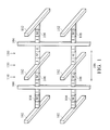
- FIG. 1 shows an exemplary scheme of an ideal RRAM 3D crossbar array architecture including 1D1R and 1S1R memory cell stacked structures.
- the MIMIM structure of the 1D1R or 1S1R memory cell structures is formed between the conductive lines 102 and 104 along the horizontal longitude 106 perpendicular to sidewalls of the conductive lines 102 and 104 .
- the RRAM 3D crossbar array architecture is usually formed within a semiconductor substrate.
- lithography processes can only be performed from the direction 110 . Performing the lithography processes from the direction 110 will not form the patterned metal layer 108 shown in FIG. 1 , which eliminates application for the 3D crossbar array architectures through the 1D1R and 1S1R memory cell structures.
- a self-rectifying RRAM cell structure including: a first electrode layer formed of a nitride of a first metal element; a second electrode layer formed of a second metal element that is different from the first metal element; and a first resistive switching layer and a second resistive switching layer.
- the first resistive switching layer is sandwiched between the first electrode layer and the second resistive switching layer, and the second resistive switching layer is sandwiched between the first resistive switching layer and the second electrode layer.
- the first resistive switching layer has a first bandgap that is lower than a second bandgap of the second resistive switching layer.
- a RRAM 3D crossbar array architecture including: a group of horizontal parallel conductive lines formed of a nitride of a first metal element; a group of vertical parallel conducive lines formed of a second metal element that is different from the first metal element; and a first resistive switching layer and a second resistive switching layer formed on sidewalls of each horizontal conductive line and in contact with the vertical conductive lines, wherein the first resistive switching layer has a first bandgap that is lower than a second bandgap of the second resistive switching layer.
- FIG. 1 shows an stereoscopic view of a RRAM 3D crossbar array architecture with 1D1R or 1S1R memory cell structures
- FIG. 2 shows a cross section of a RRAM cell structure according to an embodiment of the disclosure
- FIG. 3 shows a cross section of a RRAM cell structure according to another embodiment of the disclosure
- FIG. 4 shows a stereoscopic view of a RRAM 3D crossbar array architecture according to an embodiment of the disclosure
- FIG. 5 shows a stereoscopic view of a RRAM 3D crossbar array architecture according to another embodiment of the disclosure
- FIG. 6 shows a current-versus-voltage diagram of a RRAM cell structure according to some embodiments of the disclosure.
- first and second features are formed in direct contact
- additional features may be formed between the first and second features, such that the first and second features may not be in direct contact
- disclosure may repeat reference numerals and/or letters in the various examples. This repetition is for the purpose of simplicity and clarity and does not in itself dictate a relationship between the various embodiments and/or configurations discussed.
- the disclosure provides a RRAM cell structure without a selection device while showing self-rectifying or self-selecting characteristics similar to the RRAM having the 1D1R or 1S1R memory cell structure.
- the RRAM cell structure of the disclosure may be applicable to a 3D RRAM crossbar array architecture.
- FIG. 2 shows a memory cell structure of a resistive random access memory (RRAM) according to an embodiment of the disclosure.
- the memory cell structure of the RRAM includes a first electrode layer 202 , a first resistive switching layer 204 , a second resistive switching layer 206 and a second electrode layer 208 .
- the first resistive switching layer 204 and the second resistive switching layer 206 may be sandwiched between the first electrode layer 202 and the second electrode layer 208 .
- the first resistive switching layer 204 may abut the first electrode layer 202
- the second resistive switching layer 206 may adjacently connect to the second electrode layer 208 .
- the first electrode layer 202 may comprise a metal element.
- an oxide of the metal element of the first electrode layer 202 may be an insulator material having a lower relative bandgap.
- the second electrode layer 208 may comprise another metal element that is different from the metal element of the first electrode layer 202 .
- an oxide of another metal element of the second electrode layer 208 may be an insulator having a higher relative bandgap.
- the metal elements of the first electrode layer 202 and the second electrode layer 208 may be selected from the group consisting of Ti, Ta, Ni, Cu, W, Hf, Zr, Nb, Y, Zn, Co, Al, Si, Ge and their alloys.
- the first electrode layer 202 may be formed of Ti
- the second electrode layer 208 may be formed of Ta.
- the first electrode layer 202 may be formed of Ta
- the second electrode layer 208 may be formed of Hf.
- the first electrode layer 202 may consist of a nitride of a metal element.
- the first electrode layer 202 may be a TiN layer.
- the second electrode layer 208 may be a Ta layer.
- the electrode layers made of a nitride of metal elements have better anti-oxidizing properties.
- the first resistive switching layer 204 may be formed of an insulator having a first bandgap.
- the second resistive switching layer 206 may be an insulator, having a second bandgap that is higher than the first bandgap of the first resistive switching layer 204 .
- the first bandgap and the second bandgap may be between about 1 eV and about 9 eV.
- the second bandgap may be higher than the first bandgap by more than 0.5 eV.
- the first resistive switching layer 204 may be an oxide of the metal element of the first electrode layer 202
- the second resistive switching layer 206 may be an oxide of the metal element of the second electrode layer 208 .
- the first resistive switching layer 204 consists of TiO 2 while the first electrode layer 202 is a Ti layer or a TiN layer.
- the second resistive switching layer 206 consists of Ta 2 O 5 while the second electrode layer 208 is a Ta layer.
- the first resistive switching layer 204 consists of Ta 2 O 5 while the first electrode layer 202 is a Ta layer.
- the second resistive switching layer 206 consists of HfO 2 while the second electrode layer 208 is a Hf layer. All of the materials of the various layers of the RRAM cell structure described above can be selected from among the materials used widely in the industry.
- the first resistive switching layer 204 may be formed by directly oxidizing the outer portions of the first electrode layer 202 .
- the first resistive switching layer 204 may be directly formed from the first electrode layer 202 by thermal oxidation or laser oxidation.
- the first resistive switching layer 204 may be formed by any suitable deposition method, such as atom layer deposition (ALD), chemical vapor deposition (CVD), plasma enhanced chemical vapor deposition (PECVD), metal-organic chemical vapor deposition (MOCVD), physical vapor deposition (PVD) or other suitable deposition methods.
- ALD atom layer deposition
- CVD chemical vapor deposition
- PECVD plasma enhanced chemical vapor deposition
- MOCVD metal-organic chemical vapor deposition
- PVD physical vapor deposition
- the second resistive switching layer 206 may be formed by any suitable deposition method, such as atom layer deposition (ALD), chemical vapor deposition (CVD), plasma enhanced chemical vapor deposition (PECVD), metal-organic chemical vapor deposition (MOCVD) or physical vapor deposition (PVD) or other suitable deposition methods.
- ALD atom layer deposition
- CVD chemical vapor deposition
- PECVD plasma enhanced chemical vapor deposition
- MOCVD metal-organic chemical vapor deposition
- PVD physical vapor deposition
- the first resistive switching layer 204 may have a thickness of between about 1 nm and about 80 nm.
- the second resistive switching layer 206 may have a thickness of between about 1 nm and about 80 nm.
- FIG. 3 shows a RRAM cell structure according to another embodiment of the disclosure.
- the embodiment is similar to the structure disclosed in FIG. 2 , and the difference is that the RRAM cell structure of this embodiment further includes a third resistive switching layer 201 sandwiched between the first electrode layer 202 and the first resistive switching layer 204 .
- the third resistive switching layer 201 is a non-stoichiometric oxide of the metal element of the first electrode layer 202
- the first resistive switching layer 204 is a stoichiometric oxide of the metal element of the first electrode layer 202 .
- the first resistive switching layer 204 is a TiO 2 layer and the third resistive switching layer 201 is a TiO x layer, wherein 0 ⁇ x ⁇ 2, while the first electrode layer 202 is a Ti layer or a TiN layer.
- the aforementioned disposition of the third resistive switching layer 201 is helpful for reducing the Schottky barrier between the first resistive switching layer 204 and the first electrode layer 202 to form an ohmic contact and further to achieve the desired bipolar resistive switching (BRS) characteristics.
- BTS bipolar resistive switching
- the RRAM cell structures of the disclosure have the characteristics of having self-compliance and being self-rectifying.
- the current is rectified at the positive polarity and the sneak current is greatly suppressed.
- the RRAM cell structure of the disclosure may have a current compliance level of less than about 10 ⁇ 2 .
- the RRAM cell structure may have a current rectification ratio (i.e., the ratio of the current compliance level to the rectification current level) of greater than 10 4 at ⁇ 2 V of bias voltage.
- the current toward the second electrode layer 208 may be rectified by the second resistive switching layer 206 when the current flows thereto since the second resistive switching layer 206 has a higher bandgap than that of the first resistive switching layer 204 .
- the current that flows toward the first electrode layer 202 may easily pass through the first resistive switching layer 204 .
- the above mentioned RRAM cell structures are merely a 1R memory cell structure that has similar properties to that of a conventional resistor connected to a unidirectional selector such as the 1T1R, 1D1R, 1S1R and 1BJT1R RRAM cell structures.
- the RRAM cell structure mentioned above is not required for an initial forming step.
- the RRAM cell structure may be activated without applying an initial forming voltage.
- the initial forming voltage may sometimes damage the RRAM cell structure due to its high magnitude. Accordingly, the initial forming step-free RRAM cell structure has better reliability.
- FIG. 4 shows a RRAM cell structure applied to a 3D crossbar array architecture according to an embodiment of the disclosure.
- the RRAM 3D cross bar array architecture may comprise a group of horizontal parallel conductive lines 302 (e.g., extending along the Y longitude of FIG. 4 ), and a group of vertical parallel conductive lines 308 (e.g., extending along the Z longitude of FIG. 4 ).
- An array of RRAM cell structures is formed between the intersections of the group of horizontal parallel conductive lines 302 and the group of vertical parallel conductive lines 308 .
- Each of the RRAM cell structures may be disposed along a horizontal direction (e.g., extending along the X longitude of FIG. 4 ) perpendicular to the extending directions of the group of horizontal conductive lines 302 and the group of vertical conductive lines 308 .
- the group of horizontal parallel conductive lines 302 may be used as the first electrode layer of the RRAM cell structures, and the group of vertical parallel conductive lines 308 may be used as the second electrode layer of the RRAM cell structures.
- the group of horizontal parallel conductive lines 302 and the group of vertical parallel conductive lines 308 may respectively be formed of the same or similar materials of the first electrode layer 202 and the second electrode layer 208 described in the above embodiments.
- the group of horizontal parallel conductive lines 302 and the group of vertical parallel conductive lines 308 may respectively be fainted of the same or similar materials of the second electrode layer 208 and the first electrode layer 202 described in the above embodiments.
- the group of horizontal conductive lines 302 may be a bit line
- the group of vertical conductive lines 308 may be a word line, or vice versa.
- a first resistive switching layer 304 and a second resistive switching layer 306 are located between the horizontal conductive lines 302 and the vertical conductive lines 308 , and the first resistive switching layer 304 and the second resistive switching layer 306 may be formed on sidewalls of the vertical conductive lines 308 .
- the first resistive switching layer 304 may contact the horizontal conductive lines 302 and the second resistive switching layer 306 may contact the vertical conductive lines 308 .
- each of the RRAM cell structures is formed at the locations where the first resistive switching layer 304 and the second resistive switching layer 306 are in direct contact with each other.
- the first resistive switching layer 304 and the second resistive switching layer 306 may respectively be formed of the same or similar materials as the first resistive switching layer 204 and the second resistive switching layer 206 described in the above embodiments when the horizontal conductive lines 302 and the vertical conductive lines 308 are respectively formed of the same or similar materials as the first electrode layer 202 and the second electrode layer 208 described in the above embodiments.
- the first resistive switching layer 304 and the second resistive switching layer 306 may respectively be formed of the same or similar materials as the second resistive switching layer 206 and the first resistive switching layer 204 described in the above embodiments when the horizontal conductive lines 302 and the vertical conductive lines 308 are respectively formed of the same or similar materials as the second electrode layer 208 and the first electrode layer 202 described in the above embodiments.
- the RRAM cell structure for the 3D crossbar array architecture is formed within a semiconductor substrate.
- FIG. 5 shows a RRAM cell structure applied to a 3D crossbar array architecture according to another embodiment of the disclosure.
- the RRAM cell structure of this embodiment further includes a third resistive switching layer 301 sandwiched between the first resistive switching layer 304 and the horizontal conductive lines 302 .
- the first resistive switching layer 304 , the second resistive switching layer 306 and the third resistive switching layer 301 may respectively be formed of the same or similar materials as the first resistive switching layer 204 , the second resistive switching layer 206 , and the third resistive switching layer 201 described in the above embodiments when the horizontal conductive lines 302 and the vertical conductive lines 308 are respectively formed of the same or similar materials as the first electrode layer 202 and the second electrode layer 208 described in the above embodiments.
- the third resistive switching layer 301 may also be sandwiched between the second resistive switching layer 306 and the vertical conductive lines 308 (not illustrated) when the horizontal conductive lines 302 and the vertical conductive lines 308 are respectively formed of the same or similar materials as the second electrode layer 208 and the first electrode layer 202 described in the above embodiments.
- the first resistive switching layer 304 , the second resistive switching layer 306 and the third resistive switching layer 301 may respectively be formed of the same or similar materials as the second resistive switching layer 206 , the first resistive switching layer 204 , and the third resistive switching layer 201 described in the above embodiments.
- the RRAM 3D crossbar array architectures only include 1R memory cell structures. Therefore, the RRAM 3D crossbar array architecture may be fabricated easily since the 1R memory cell structures do not require an inter-metal layer.
- the problem of sneak current occurring in the 1R memory cell structures of the conventional RRAM 3D crossbar array may be overcome because the 1R memory cell structures of the disclosure having characteristics such as self-compliance and being self-rectifying. Therefore, the RRAM 3D crossbar array architecture according to the disclosure can be used as a next-generation nonvolatile memory and has great potential to replace flash memory devices.
- FIG. 6 shows a current-versus-voltage diagram of the RRAM according to some embodiments of the disclosure.
- the RRAM is formed of a Ta layer, a Ta 2 O 5 layer, a TiO 2 layer, and a TiN layer which are stacked in order.
- the RRAM is formed of a Ta layer, a Ta 2 O 5 layer, a TiO 2 layer, a TiOx layer, and a TiN layer which are stacked in order, wherein 0 ⁇ x ⁇ 2.
- the RRAMs of the embodiments of the disclosure clearly show self-rectification characteristics.
- the RRAMs may be placed in a set state by applying a positive voltage, and a reset state by applying a negative voltage, which shows that the RRAMs according to the disclosure are a bipolar resistive switching memory.
- the RRAMs can be placed in the set state and the reset state by a minimum voltage of about +4 V and ⁇ 4 V, respectively ( ⁇ 2 V is used to read and not to set/reset the device). It can also be found that the RRAM of the disclosure may have a current compliance level below 10 ⁇ 2 when the negative voltage is increased, even to ⁇ 4 V.
Abstract
The present disclosure provides a self-rectifying RRAM cell structure including a first electrode layer formed of a nitride of a first metal element, a second electrode layer formed of a second metal element that is different from the first metal element, a first resistive switching layer and a second resistive switching layer. The first resistive switching layer is sandwiched between the first electrode layer and the second resistive switching layer, and the second resistive switching layer is sandwiched between the first resistive switching layer and the second electrode layer. The first resistive switching layer has a first bandgap that is lower than the second bandgap of the second resistive switching layer. Furthermore, a RRAM 3D crossbar array architecture is also provided.
Description
This application claims the benefit of Taiwan Patent Application No. 103129478 filed on Aug. 27, 2014, entitled “SELF-RECTIFYING RRAM CELL STRUCTURE AND RRAM 3D CROSSBAR ARRAY ARCHITECTURE” which is hereby incorporated herein by reference.
Field of the Disclosure
The present disclosure relates to a memory device, and in particular, it relates to a resistive random access memory (RRAM) cell structure and a 3D crossbar array thereof.
Description of the Related Art
As the functionality of integrated chips increases, the need for more memory also increases. Designers have been looking to decrease the size of the memory element and stack more memory elements in a unit area to achieve greater capacity and lower costs per bit. In the past few decades, the aggressive shrinkage of memory elements is due to advancements in lithography techniques. Flash memory has been widely used as large-capacity, inexpensive nonvolatile memory which can store data even when it is powered off. In addition, flash memory can achieve high density by using 3D arrays, such as by using vertical NAND memory cell stacking. However, it has been found that further miniaturization of flash memory is limited due to the increasing cost.
Designers are now looking at next-generation nonvolatile memories such as MRAMs (Magnetoresistive Random Access Memory), PCRAMs (Phase Change Random Access Memory), CBRAMs (Conductive Bridging Random Access Memory) and RRAMs (Resistive Random Access Memory), to increase writing speeds and decrease power consumption. Among the nonvolatile memories, the RRAM has the greatest potential to replace flash memories due to its simple structure, simple crossbar array and suitability for low-temperature fabrication. A unit element of the RRAM is composed of only an insulator with two metal electrodes.
Although the RRAM crossbar array architecture is simple, there are still many problems that need to be overcome for fabrication, especially for three-dimensional (3D) crossbar array architectures. Without a vertical 3D architecture, the RRAM will most likely not be able to compete with 3D NAND memories in terms of bit cost for mass data storage.
The RRAM crossbar array architectures based on resistive switching elements theoretically allows for the smallest cell size of 4F2 where F is the minimum feature size, and the low-temperature fabrication enables stacking of memory arrays three-dimensionally, for unprecedented high-integration density. However, in the 1R structure (having a resistive element only), undesired sneak current that flows through neighboring unselected memory cells significantly deteriorates the read margin, and limits the maximum size of the crossbar array to below 64 bits. This problem can be mitigated by additional nonlinear selection devices in series with the resistive switching elements. Some memory cell structures, such as one diode-one resistor (1D1R), one bipolar selector-one resistor (1S1R), one MOSFET transistor-one resistor (1T1R), and one bipolar junction transistor-one resistor 1BJT1R memory cell structures, have been developed. Among the memory cell structures, the 1T1R and 1BJT1R memory cell structures are undesirable because of the complicated and high-temperature fabrication requirements of MOSFETs and BJTs, while the complementary resistive switching (CRS) memory cell structure suffers from the issue of destructive read. Hence, the 1D1R and 1S1R memory cell structures appear to be the leading contenders for the 3D crossbar array architectures.
However, the 3D crossbar array architectures of the 1D1R or 1S1R memory cell structures still cannot be successfully fabricated. The 1D1R and 1S1R memory cell structures are basically formed of a metal-insulator-metal-insulator-metal (MIMIM) structure. FIG. 1 shows an exemplary scheme of an ideal RRAM 3D crossbar array architecture including 1D1R and 1S1R memory cell stacked structures. The MIMIM structure of the 1D1R or 1S1R memory cell structures is formed between the conductive lines 102 and 104 along the horizontal longitude 106 perpendicular to sidewalls of the conductive lines 102 and 104. However, the RRAM 3D crossbar array architecture is usually formed within a semiconductor substrate. After the formation of the conductive lines 102, lithography processes can only be performed from the direction 110. Performing the lithography processes from the direction 110 will not form the patterned metal layer 108 shown in FIG. 1 , which eliminates application for the 3D crossbar array architectures through the 1D1R and 1S1R memory cell structures.
In some embodiments of the disclosure, a self-rectifying RRAM cell structure is provided, including: a first electrode layer formed of a nitride of a first metal element; a second electrode layer formed of a second metal element that is different from the first metal element; and a first resistive switching layer and a second resistive switching layer. The first resistive switching layer is sandwiched between the first electrode layer and the second resistive switching layer, and the second resistive switching layer is sandwiched between the first resistive switching layer and the second electrode layer. The first resistive switching layer has a first bandgap that is lower than a second bandgap of the second resistive switching layer.
In some embodiments of the disclosure, a RRAM 3D crossbar array architecture is provided, including: a group of horizontal parallel conductive lines formed of a nitride of a first metal element; a group of vertical parallel conducive lines formed of a second metal element that is different from the first metal element; and a first resistive switching layer and a second resistive switching layer formed on sidewalls of each horizontal conductive line and in contact with the vertical conductive lines, wherein the first resistive switching layer has a first bandgap that is lower than a second bandgap of the second resistive switching layer.
A detailed description is given in the following embodiments with reference to the accompanying drawings.
The present disclosure can be further understood by reading the subsequent detailed description and examples with references made to the accompanying drawings, wherein:
The following description is of the best-contemplated mode of carrying out the disclosure. This description is made for the purpose of illustrating the general principles of the disclosure and should not be taken in a limiting sense. These are, of course, merely examples and are not intended to be limited. For example, the formation of a first feature over, above, below, or on a second feature in the description that follows may include embodiments in which the first and second features are formed in direct contact, and may also include embodiments in which additional features may be formed between the first and second features, such that the first and second features may not be in direct contact. In addition, the disclosure may repeat reference numerals and/or letters in the various examples. This repetition is for the purpose of simplicity and clarity and does not in itself dictate a relationship between the various embodiments and/or configurations discussed.
The disclosure provides a RRAM cell structure without a selection device while showing self-rectifying or self-selecting characteristics similar to the RRAM having the 1D1R or 1S1R memory cell structure. In addition, the RRAM cell structure of the disclosure may be applicable to a 3D RRAM crossbar array architecture.
The first electrode layer 202 may comprise a metal element. In an embodiment, an oxide of the metal element of the first electrode layer 202 may be an insulator material having a lower relative bandgap. The second electrode layer 208 may comprise another metal element that is different from the metal element of the first electrode layer 202. In addition, an oxide of another metal element of the second electrode layer 208 may be an insulator having a higher relative bandgap. The metal elements of the first electrode layer 202 and the second electrode layer 208 may be selected from the group consisting of Ti, Ta, Ni, Cu, W, Hf, Zr, Nb, Y, Zn, Co, Al, Si, Ge and their alloys. For example, in an embodiment, the first electrode layer 202 may be formed of Ti, and the second electrode layer 208 may be formed of Ta. In another embodiment, the first electrode layer 202 may be formed of Ta, and the second electrode layer 208 may be formed of Hf.
In another embodiment of the disclosure, the first electrode layer 202 may consist of a nitride of a metal element. For example, the first electrode layer 202 may be a TiN layer. In addition, the second electrode layer 208 may be a Ta layer. Compared to the electrode layers consisting of pure metal elements (for example, Ti), the electrode layers made of a nitride of metal elements (for example, TiN) have better anti-oxidizing properties.
The first resistive switching layer 204 may be formed of an insulator having a first bandgap. The second resistive switching layer 206 may be an insulator, having a second bandgap that is higher than the first bandgap of the first resistive switching layer 204. In an embodiment, the first bandgap and the second bandgap may be between about 1 eV and about 9 eV. In some embodiments, the second bandgap may be higher than the first bandgap by more than 0.5 eV.
In some embodiments, the first resistive switching layer 204 may be an oxide of the metal element of the first electrode layer 202, and the second resistive switching layer 206 may be an oxide of the metal element of the second electrode layer 208. For example, in an embodiment, the first resistive switching layer 204 consists of TiO2 while the first electrode layer 202 is a Ti layer or a TiN layer. In addition, the second resistive switching layer 206 consists of Ta2O5 while the second electrode layer 208 is a Ta layer. In another embodiment, the first resistive switching layer 204 consists of Ta2O5 while the first electrode layer 202 is a Ta layer. In addition, the second resistive switching layer 206 consists of HfO2 while the second electrode layer 208 is a Hf layer. All of the materials of the various layers of the RRAM cell structure described above can be selected from among the materials used widely in the industry.
In an embodiment, the first resistive switching layer 204 may be formed by directly oxidizing the outer portions of the first electrode layer 202. For example, the first resistive switching layer 204 may be directly formed from the first electrode layer 202 by thermal oxidation or laser oxidation. In other embodiments, the first resistive switching layer 204 may be formed by any suitable deposition method, such as atom layer deposition (ALD), chemical vapor deposition (CVD), plasma enhanced chemical vapor deposition (PECVD), metal-organic chemical vapor deposition (MOCVD), physical vapor deposition (PVD) or other suitable deposition methods. The second resistive switching layer 206 may be formed by any suitable deposition method, such as atom layer deposition (ALD), chemical vapor deposition (CVD), plasma enhanced chemical vapor deposition (PECVD), metal-organic chemical vapor deposition (MOCVD) or physical vapor deposition (PVD) or other suitable deposition methods. In some embodiments, the first resistive switching layer 204 may have a thickness of between about 1 nm and about 80 nm. The second resistive switching layer 206 may have a thickness of between about 1 nm and about 80 nm.
Refer to FIG. 3 , which shows a RRAM cell structure according to another embodiment of the disclosure. The embodiment is similar to the structure disclosed in FIG. 2 , and the difference is that the RRAM cell structure of this embodiment further includes a third resistive switching layer 201 sandwiched between the first electrode layer 202 and the first resistive switching layer 204. In this embodiment, the third resistive switching layer 201 is a non-stoichiometric oxide of the metal element of the first electrode layer 202, and the first resistive switching layer 204 is a stoichiometric oxide of the metal element of the first electrode layer 202. For example, the first resistive switching layer 204 is a TiO2 layer and the third resistive switching layer 201 is a TiOx layer, wherein 0<x<2, while the first electrode layer 202 is a Ti layer or a TiN layer. The aforementioned disposition of the third resistive switching layer 201 is helpful for reducing the Schottky barrier between the first resistive switching layer 204 and the first electrode layer 202 to form an ohmic contact and further to achieve the desired bipolar resistive switching (BRS) characteristics.
Furthermore, the RRAM cell structures of the disclosure have the characteristics of having self-compliance and being self-rectifying. The current is rectified at the positive polarity and the sneak current is greatly suppressed. For example, the RRAM cell structure of the disclosure may have a current compliance level of less than about 10−2. The RRAM cell structure may have a current rectification ratio (i.e., the ratio of the current compliance level to the rectification current level) of greater than 104 at ±2 V of bias voltage. In some embodiments, the current toward the second electrode layer 208 may be rectified by the second resistive switching layer 206 when the current flows thereto since the second resistive switching layer 206 has a higher bandgap than that of the first resistive switching layer 204. The current that flows toward the first electrode layer 202 may easily pass through the first resistive switching layer 204.
Therefore, the above mentioned RRAM cell structures are merely a 1R memory cell structure that has similar properties to that of a conventional resistor connected to a unidirectional selector such as the 1T1R, 1D1R, 1S1R and 1BJT1R RRAM cell structures. In addition, the RRAM cell structure mentioned above is not required for an initial forming step. The RRAM cell structure may be activated without applying an initial forming voltage. The initial forming voltage may sometimes damage the RRAM cell structure due to its high magnitude. Accordingly, the initial forming step-free RRAM cell structure has better reliability.
In an embodiment, the group of horizontal parallel conductive lines 302 may be used as the first electrode layer of the RRAM cell structures, and the group of vertical parallel conductive lines 308 may be used as the second electrode layer of the RRAM cell structures. The group of horizontal parallel conductive lines 302 and the group of vertical parallel conductive lines 308 may respectively be formed of the same or similar materials of the first electrode layer 202 and the second electrode layer 208 described in the above embodiments. Alternatively, the group of horizontal parallel conductive lines 302 and the group of vertical parallel conductive lines 308 may respectively be fainted of the same or similar materials of the second electrode layer 208 and the first electrode layer 202 described in the above embodiments. In an embodiment, the group of horizontal conductive lines 302 may be a bit line, and the group of vertical conductive lines 308 may be a word line, or vice versa.
A first resistive switching layer 304 and a second resistive switching layer 306 are located between the horizontal conductive lines 302 and the vertical conductive lines 308, and the first resistive switching layer 304 and the second resistive switching layer 306 may be formed on sidewalls of the vertical conductive lines 308. In which, the first resistive switching layer 304 may contact the horizontal conductive lines 302 and the second resistive switching layer 306 may contact the vertical conductive lines 308. In other words, each of the RRAM cell structures is formed at the locations where the first resistive switching layer 304 and the second resistive switching layer 306 are in direct contact with each other. In an embodiment, the first resistive switching layer 304 and the second resistive switching layer 306 may respectively be formed of the same or similar materials as the first resistive switching layer 204 and the second resistive switching layer 206 described in the above embodiments when the horizontal conductive lines 302 and the vertical conductive lines 308 are respectively formed of the same or similar materials as the first electrode layer 202 and the second electrode layer 208 described in the above embodiments. Alternatively, the first resistive switching layer 304 and the second resistive switching layer 306 may respectively be formed of the same or similar materials as the second resistive switching layer 206 and the first resistive switching layer 204 described in the above embodiments when the horizontal conductive lines 302 and the vertical conductive lines 308 are respectively formed of the same or similar materials as the second electrode layer 208 and the first electrode layer 202 described in the above embodiments. In some embodiments, the RRAM cell structure for the 3D crossbar array architecture is formed within a semiconductor substrate.
Refer to FIG. 5 , which shows a RRAM cell structure applied to a 3D crossbar array architecture according to another embodiment of the disclosure. The difference between this embodiment and that of FIG. 4 is that the RRAM cell structure of this embodiment further includes a third resistive switching layer 301 sandwiched between the first resistive switching layer 304 and the horizontal conductive lines 302. In this embodiment, the first resistive switching layer 304, the second resistive switching layer 306 and the third resistive switching layer 301 may respectively be formed of the same or similar materials as the first resistive switching layer 204, the second resistive switching layer 206, and the third resistive switching layer 201 described in the above embodiments when the horizontal conductive lines 302 and the vertical conductive lines 308 are respectively formed of the same or similar materials as the first electrode layer 202 and the second electrode layer 208 described in the above embodiments.
It will be appreciated that the disclosure is not limited to the configurations mentioned above. In other embodiments, the third resistive switching layer 301 may also be sandwiched between the second resistive switching layer 306 and the vertical conductive lines 308 (not illustrated) when the horizontal conductive lines 302 and the vertical conductive lines 308 are respectively formed of the same or similar materials as the second electrode layer 208 and the first electrode layer 202 described in the above embodiments. In this embodiment, the first resistive switching layer 304, the second resistive switching layer 306 and the third resistive switching layer 301 may respectively be formed of the same or similar materials as the second resistive switching layer 206, the first resistive switching layer 204, and the third resistive switching layer 201 described in the above embodiments.
As shown in FIGS. 4 and 5 , the RRAM 3D crossbar array architectures only include 1R memory cell structures. Therefore, the RRAM 3D crossbar array architecture may be fabricated easily since the 1R memory cell structures do not require an inter-metal layer. The problem of sneak current occurring in the 1R memory cell structures of the conventional RRAM 3D crossbar array may be overcome because the 1R memory cell structures of the disclosure having characteristics such as self-compliance and being self-rectifying. Therefore, the RRAM 3D crossbar array architecture according to the disclosure can be used as a next-generation nonvolatile memory and has great potential to replace flash memory devices.
As shown in FIG. 6 , the RRAMs of the embodiments of the disclosure clearly show self-rectification characteristics. In addition, the RRAMs may be placed in a set state by applying a positive voltage, and a reset state by applying a negative voltage, which shows that the RRAMs according to the disclosure are a bipolar resistive switching memory. The RRAMs can be placed in the set state and the reset state by a minimum voltage of about +4 V and −4 V, respectively (±2 V is used to read and not to set/reset the device). It can also be found that the RRAM of the disclosure may have a current compliance level below 10−2 when the negative voltage is increased, even to −4 V.
While the disclosure has been described by way of example and in terms of the preferred embodiments, it is to be understood that the disclosure is not limited to the disclosed embodiments. On the contrary, it is intended to cover various modifications and similar arrangements (as would be apparent to those skilled in the art). Therefore, the scope of the appended claims should be accorded the broadest interpretation so as to encompass all such modifications and similar arrangements.
Claims (11)
1. A self-rectifying RRAM cell structure, comprising:
a first electrode layer formed of a nitride of a first metal element;
a first resistive switching layer disposed on the first electrode layer, wherein the first resistive switching layer is formed of an oxide of the first metal element;
a second resistive switching layer disposed on the first resistive switching layer, wherein the first resistive switching layer has a first bandgap that is lower than a second bandgap of the second resistive switching layer;
a second electrode layer disposed on the second resistive switching layer and formed of a second metal element that is different from the first metal element, wherein the second resistive switching layer is formed of an oxide of the second metal element; and
a third resistive switching layer sandwiched between the first resistive switching layer and the first electrode layer, wherein the third resistive switching layer is a non-stoichiometric oxide of the first metal element, and the first resistive switching layer is a stoichiometric oxide of the first metal element.
2. The self-rectifying RRAM cell structure as claimed in claim 1 , wherein the first metal element and the second metal element are respectively selected from a group consisting of Ti, Ta, Ni, Cu, W, Hf, Zr, Nb, Y, Zn, Co, Al, Si, Ge and their alloys.
3. The self-rectifying RRAM cell structure as claimed in claim 1 , wherein the first resistive switching layer is a TiO2 layer, the second resistive switching layer is a Ta2O5 layer, and the third resistive switching layer is a TiOx layer, wherein 0<x<2.
4. The self-rectifying RRAM cell structure as claimed in claim 1 , wherein the self-rectifying RRAM cell structure is a bipolar resistive switching memory.
5. The self-rectifying RRAM cell structure as claimed in claim 1 , wherein the second bandgap is higher than the first bandgap by more than about 0.5 eV.
6. A RRAM 3D crossbar array architecture, comprising:
a group of horizontal parallel conductive lines formed of a nitride of a first metal element;
a group of vertical parallel conducive lines formed of a second metal element that is different from the first metal element;
a first resistive switching layer and a second resistive switching layer formed on sidewalls of each of the horizontal parallel conductive line and in contact with the group of vertical parallel conductive lines, wherein the first resistive switching layer has a first bandgap that is lower than a second bandgap of the second resistive switching layer, and wherein the first resistive switching layer consists of an oxide of the first metal element, and the second resistive switching layer consists of an oxide of the second metal element; and
a third resistive switching layer disposed between the first resistive switching layer and the horizontal parallel conductive lines that correspond to the first resistive switching layer, wherein the third resistive switching layer is a non-stoichiometric oxide of the first metal element, and the first resistive switching layer is a stoichiometric oxide of the first metal element.
7. The RRAM 3D crossbar array architecture as claimed in claim 6 , wherein the first resistive switching layer is a TiO2 layer, the second resistive switching layer is a Ta2O5 layer, and the third resistive switching layer is a TiOx layer, wherein 0<x<2.
8. The RRAM 3D crossbar array architecture as claimed in claim 6 , wherein the first metal element and the second metal element are respectively selected from a group consisting of Ti, Ta, Ni, Cu, W, Hf, Zr, Nb, Y, Zn, Co, Al, Si, Ge and their alloys.
9. The RRAM 3D crossbar array architecture as claimed in claim 6 , wherein the second bandgap is higher than the first bandgap by more than about 0.5 eV.
10. The RRAM 3D crossbar array architecture as claimed in claim 6 , wherein the group of horizontal parallel conductive lines are bit lines, and the group of vertical parallel conductive lines are word lines.
11. The RRAM 3D crossbar array architecture as claimed in claim 6 , wherein the group of horizontal parallel conductive lines are word lines, and the group of vertical parallel conductive lines are bit lines.
Applications Claiming Priority (3)
| Application Number | Priority Date | Filing Date | Title |
|---|---|---|---|
| TW103129478A | 2014-08-27 | ||
| TW103129478A TWI529987B (en) | 2014-08-27 | 2014-08-27 | Self-rectfying rram cell strcutre and rram 3d crossbar array architecture |
| TW103129478 | 2014-08-27 |
Publications (2)
| Publication Number | Publication Date |
|---|---|
| US20160064453A1 US20160064453A1 (en) | 2016-03-03 |
| US10056432B2 true US10056432B2 (en) | 2018-08-21 |
Family
ID=55403447
Family Applications (1)
| Application Number | Title | Priority Date | Filing Date |
|---|---|---|---|
| US14/731,933 Active US10056432B2 (en) | 2014-08-27 | 2015-06-05 | Self-rectifying RRAM cell structure having two resistive switching layers with different bandgaps and RRAM 3D crossbar array architecture |
Country Status (2)
| Country | Link |
|---|---|
| US (1) | US10056432B2 (en) |
| TW (1) | TWI529987B (en) |
Cited By (1)
| Publication number | Priority date | Publication date | Assignee | Title |
|---|---|---|---|---|
| US10847578B1 (en) | 2019-07-03 | 2020-11-24 | Windbond Electronics Corp. | Three-dimensional resistive memories and methods for forming the same |
Families Citing this family (12)
| Publication number | Priority date | Publication date | Assignee | Title |
|---|---|---|---|---|
| JP6386349B2 (en) * | 2014-11-19 | 2018-09-05 | 東芝メモリ株式会社 | Nonvolatile memory device |
| WO2017222525A1 (en) * | 2016-06-23 | 2017-12-28 | Intel Corporation | Rram devices with two-sided intrinsic ballast |
| WO2018063164A1 (en) * | 2016-09-27 | 2018-04-05 | Intel Corporation | Diode based resistive random access memory |
| US10127494B1 (en) | 2017-08-02 | 2018-11-13 | Google Llc | Neural network crossbar stack |
| US10490602B2 (en) * | 2017-09-21 | 2019-11-26 | Micron Technology, Inc. | Three dimensional memory arrays |
| US10176866B1 (en) * | 2017-09-25 | 2019-01-08 | Taiwan Semiconductor Manufacturing Co., Ltd. | Recap layer scheme to enhance RRAM performance |
| KR102126791B1 (en) * | 2017-11-23 | 2020-06-25 | 서울대학교산학협력단 | Neural networks using cross-point array and pattern readout method thereof |
| US10497752B1 (en) | 2018-05-11 | 2019-12-03 | International Business Machines Corporation | Resistive random-access memory array with reduced switching resistance variability |
| EP3886104B1 (en) | 2020-03-26 | 2024-01-24 | Centre National de la Recherche Scientifique | Resistive random memory architecture with high integration density and control method thereof |
| US11404636B2 (en) * | 2020-04-24 | 2022-08-02 | Applied Materials, Inc | Crested barrier device and synaptic element |
| US11289157B1 (en) | 2020-09-04 | 2022-03-29 | Winbond Electronics Corp. | Memory device |
| US11825754B2 (en) * | 2021-05-27 | 2023-11-21 | Micron Technology, Inc. | Memory cells with sidewall and bulk regions in planar structures |
Citations (8)
| Publication number | Priority date | Publication date | Assignee | Title |
|---|---|---|---|---|
| CN102610616A (en) | 2011-01-19 | 2012-07-25 | 旺宏电子股份有限公司 | Low cost scalable 3d memory |
| US20130034947A1 (en) | 2011-08-05 | 2013-02-07 | Intermolecular, Inc. | Atomic layer deposition of metal oxides for memory applications |
| US8373149B2 (en) * | 2008-04-07 | 2013-02-12 | Nec Corporation | Resistance change element and manufacturing method thereof |
| US20130221314A1 (en) * | 2012-02-28 | 2013-08-29 | Intermolecular, Inc. | Memory Device Having An Integrated Two-Terminal Current Limiting Resistor |
| US8658511B1 (en) * | 2012-12-20 | 2014-02-25 | Intermolecular, Inc. | Etching resistive switching and electrode layers |
| CN103872245A (en) | 2012-12-10 | 2014-06-18 | 华邦电子股份有限公司 | Self-rectifying rram storage cell structure and 3d crossbar array architecture thereof |
| CN103988264A (en) | 2011-10-17 | 2014-08-13 | 桑迪士克3D有限责任公司 | Non-volatile memory cell comprising metal oxide resistive memory element and an antifuse layer |
| US20150179937A1 (en) * | 2013-12-23 | 2015-06-25 | Intermolecular Inc. | Metal Organic Chemical Vapor Deposition of Embedded Resistors for ReRAM Cells |
-
2014
- 2014-08-27 TW TW103129478A patent/TWI529987B/en active
-
2015
- 2015-06-05 US US14/731,933 patent/US10056432B2/en active Active
Patent Citations (8)
| Publication number | Priority date | Publication date | Assignee | Title |
|---|---|---|---|---|
| US8373149B2 (en) * | 2008-04-07 | 2013-02-12 | Nec Corporation | Resistance change element and manufacturing method thereof |
| CN102610616A (en) | 2011-01-19 | 2012-07-25 | 旺宏电子股份有限公司 | Low cost scalable 3d memory |
| US20130034947A1 (en) | 2011-08-05 | 2013-02-07 | Intermolecular, Inc. | Atomic layer deposition of metal oxides for memory applications |
| CN103988264A (en) | 2011-10-17 | 2014-08-13 | 桑迪士克3D有限责任公司 | Non-volatile memory cell comprising metal oxide resistive memory element and an antifuse layer |
| US20130221314A1 (en) * | 2012-02-28 | 2013-08-29 | Intermolecular, Inc. | Memory Device Having An Integrated Two-Terminal Current Limiting Resistor |
| CN103872245A (en) | 2012-12-10 | 2014-06-18 | 华邦电子股份有限公司 | Self-rectifying rram storage cell structure and 3d crossbar array architecture thereof |
| US8658511B1 (en) * | 2012-12-20 | 2014-02-25 | Intermolecular, Inc. | Etching resistive switching and electrode layers |
| US20150179937A1 (en) * | 2013-12-23 | 2015-06-25 | Intermolecular Inc. | Metal Organic Chemical Vapor Deposition of Embedded Resistors for ReRAM Cells |
Non-Patent Citations (1)
| Title |
|---|
| https://en.wikipedia.org/wiki/Metalorganic_vapour_phase_epitaxy. * |
Cited By (1)
| Publication number | Priority date | Publication date | Assignee | Title |
|---|---|---|---|---|
| US10847578B1 (en) | 2019-07-03 | 2020-11-24 | Windbond Electronics Corp. | Three-dimensional resistive memories and methods for forming the same |
Also Published As
| Publication number | Publication date |
|---|---|
| TWI529987B (en) | 2016-04-11 |
| TW201608750A (en) | 2016-03-01 |
| US20160064453A1 (en) | 2016-03-03 |
Similar Documents
| Publication | Publication Date | Title |
|---|---|---|
| US10056432B2 (en) | Self-rectifying RRAM cell structure having two resistive switching layers with different bandgaps and RRAM 3D crossbar array architecture | |
| US9059391B2 (en) | Self-rectifying RRAM cell structure and 3D crossbar array architecture thereof | |
| KR102514350B1 (en) | switch element and memory | |
| US9978941B2 (en) | Self-rectifying resistive random access memory cell structure | |
| CN103238185B (en) | Non-volatile semiconductor storage device and write method for same | |
| KR20170134381A (en) | Switch element and storage device | |
| JP2011040483A (en) | Resistance-change memory | |
| JP2008010836A (en) | Variable resistance random access memory element equipped with n+ interface layer | |
| US8937830B2 (en) | Semiconductor memory device | |
| US20140306173A1 (en) | Resistive memory and method for fabricating the same | |
| US20200411759A1 (en) | Switch device, storage apparatus, and memory system | |
| US8559210B2 (en) | Memory device | |
| US20150137062A1 (en) | Mimcaps with quantum wells as selector elements for crossbar memory arrays | |
| KR102462182B1 (en) | store | |
| JP6606177B2 (en) | Devices containing metal chalcogenides | |
| US20230070508A1 (en) | Increasing selector surface area in crossbar array circuits | |
| KR101471971B1 (en) | Non-linear resistance switching memory device using multi-layered tunnel barrier selector | |
| TWI733520B (en) | Memory cell, memory device and method of amplifying data using selector element of memory cell | |
| TWI597824B (en) | Resistive random-access memory and operation of resistive random-access memory | |
| CN105470277B (en) | Self-rectifying resistive random access memory memory cell structure and 3D are staggered | |
| Oh et al. | An access-transistor-free resistive random access memory (RRAM) using a GST/TiO 2 stack and its novel access mechanism | |
| KR20130142411A (en) | Resistive random access memory device |
Legal Events
| Date | Code | Title | Description |
|---|---|---|---|
| AS | Assignment |
Owner name: WINBOND ELECTRONICS CORP., TAIWAN Free format text: ASSIGNMENT OF ASSIGNORS INTEREST;ASSIGNORS:HOU, TUO-HUNG;HSU, CHUNG-WEI;CHOU, CHUN-TSE;AND OTHERS;REEL/FRAME:035824/0495 Effective date: 20150521 |
|
| STCF | Information on status: patent grant |
Free format text: PATENTED CASE |
|
| MAFP | Maintenance fee payment |
Free format text: PAYMENT OF MAINTENANCE FEE, 4TH YEAR, LARGE ENTITY (ORIGINAL EVENT CODE: M1551); ENTITY STATUS OF PATENT OWNER: LARGE ENTITY Year of fee payment: 4 |