US10032803B2 - Thin film transistor array panel and method for manufacturing the same - Google Patents
Thin film transistor array panel and method for manufacturing the same Download PDFInfo
- Publication number
- US10032803B2 US10032803B2 US15/343,780 US201615343780A US10032803B2 US 10032803 B2 US10032803 B2 US 10032803B2 US 201615343780 A US201615343780 A US 201615343780A US 10032803 B2 US10032803 B2 US 10032803B2
- Authority
- US
- United States
- Prior art keywords
- layer
- forming
- source
- passivation layer
- drain electrodes
- Prior art date
- Legal status (The legal status is an assumption and is not a legal conclusion. Google has not performed a legal analysis and makes no representation as to the accuracy of the status listed.)
- Active
Links
- 239000010409 thin film Substances 0.000 title claims abstract description 37
- 238000000034 method Methods 0.000 title claims description 29
- 238000004519 manufacturing process Methods 0.000 title claims description 9
- 238000002161 passivation Methods 0.000 claims abstract description 58
- 229910052751 metal Inorganic materials 0.000 claims abstract description 54
- 239000002184 metal Substances 0.000 claims abstract description 54
- 239000004065 semiconductor Substances 0.000 claims abstract description 42
- 229910021332 silicide Inorganic materials 0.000 claims abstract description 21
- FVBUAEGBCNSCDD-UHFFFAOYSA-N silicide(4-) Chemical compound [Si-4] FVBUAEGBCNSCDD-UHFFFAOYSA-N 0.000 claims abstract description 21
- 239000000758 substrate Substances 0.000 claims abstract description 16
- BLRPTPMANUNPDV-UHFFFAOYSA-N Silane Chemical compound [SiH4] BLRPTPMANUNPDV-UHFFFAOYSA-N 0.000 claims description 34
- 229910000077 silane Inorganic materials 0.000 claims description 34
- 239000000463 material Substances 0.000 claims description 30
- 239000010949 copper Substances 0.000 claims description 19
- RYGMFSIKBFXOCR-UHFFFAOYSA-N Copper Chemical compound [Cu] RYGMFSIKBFXOCR-UHFFFAOYSA-N 0.000 claims description 17
- VYPSYNLAJGMNEJ-UHFFFAOYSA-N Silicium dioxide Chemical compound O=[Si]=O VYPSYNLAJGMNEJ-UHFFFAOYSA-N 0.000 claims description 17
- 229910052802 copper Inorganic materials 0.000 claims description 17
- 229910052814 silicon oxide Inorganic materials 0.000 claims description 17
- 229910044991 metal oxide Inorganic materials 0.000 claims description 15
- 150000004706 metal oxides Chemical class 0.000 claims description 15
- 229910000881 Cu alloy Inorganic materials 0.000 claims description 11
- 230000004888 barrier function Effects 0.000 claims description 11
- 229910052581 Si3N4 Inorganic materials 0.000 claims description 9
- HQVNEWCFYHHQES-UHFFFAOYSA-N silicon nitride Chemical compound N12[Si]34N5[Si]62N3[Si]51N64 HQVNEWCFYHHQES-UHFFFAOYSA-N 0.000 claims description 9
- 238000005229 chemical vapour deposition Methods 0.000 claims description 5
- 229910052710 silicon Inorganic materials 0.000 claims description 5
- 239000010703 silicon Substances 0.000 claims description 5
- 206010010144 Completed suicide Diseases 0.000 abstract description 4
- 239000010410 layer Substances 0.000 description 229
- 229920002120 photoresistant polymer Polymers 0.000 description 18
- 239000004973 liquid crystal related substance Substances 0.000 description 8
- 230000000903 blocking effect Effects 0.000 description 7
- 239000010936 titanium Substances 0.000 description 7
- RTAQQCXQSZGOHL-UHFFFAOYSA-N Titanium Chemical compound [Ti] RTAQQCXQSZGOHL-UHFFFAOYSA-N 0.000 description 5
- 239000011651 chromium Substances 0.000 description 5
- 239000011572 manganese Substances 0.000 description 5
- 229910052719 titanium Inorganic materials 0.000 description 5
- XLOMVQKBTHCTTD-UHFFFAOYSA-N zinc oxide Inorganic materials [Zn]=O XLOMVQKBTHCTTD-UHFFFAOYSA-N 0.000 description 5
- 239000011787 zinc oxide Substances 0.000 description 5
- ZOKXTWBITQBERF-UHFFFAOYSA-N Molybdenum Chemical compound [Mo] ZOKXTWBITQBERF-UHFFFAOYSA-N 0.000 description 4
- XUIMIQQOPSSXEZ-UHFFFAOYSA-N Silicon Chemical compound [Si] XUIMIQQOPSSXEZ-UHFFFAOYSA-N 0.000 description 4
- BQCADISMDOOEFD-UHFFFAOYSA-N Silver Chemical compound [Ag] BQCADISMDOOEFD-UHFFFAOYSA-N 0.000 description 4
- 229910052782 aluminium Inorganic materials 0.000 description 4
- XAGFODPZIPBFFR-UHFFFAOYSA-N aluminium Chemical compound [Al] XAGFODPZIPBFFR-UHFFFAOYSA-N 0.000 description 4
- 239000003086 colorant Substances 0.000 description 4
- 238000009413 insulation Methods 0.000 description 4
- 229910052750 molybdenum Inorganic materials 0.000 description 4
- 239000011733 molybdenum Substances 0.000 description 4
- 229910052709 silver Inorganic materials 0.000 description 4
- 239000004332 silver Substances 0.000 description 4
- YVTHLONGBIQYBO-UHFFFAOYSA-N zinc indium(3+) oxygen(2-) Chemical compound [O--].[Zn++].[In+3] YVTHLONGBIQYBO-UHFFFAOYSA-N 0.000 description 4
- VYZAMTAEIAYCRO-UHFFFAOYSA-N Chromium Chemical compound [Cr] VYZAMTAEIAYCRO-UHFFFAOYSA-N 0.000 description 3
- PWHULOQIROXLJO-UHFFFAOYSA-N Manganese Chemical compound [Mn] PWHULOQIROXLJO-UHFFFAOYSA-N 0.000 description 3
- 239000003990 capacitor Substances 0.000 description 3
- 229910052804 chromium Inorganic materials 0.000 description 3
- JAONJTDQXUSBGG-UHFFFAOYSA-N dialuminum;dizinc;oxygen(2-) Chemical compound [O-2].[O-2].[O-2].[O-2].[O-2].[Al+3].[Al+3].[Zn+2].[Zn+2] JAONJTDQXUSBGG-UHFFFAOYSA-N 0.000 description 3
- 239000011521 glass Substances 0.000 description 3
- 239000012212 insulator Substances 0.000 description 3
- 229910052748 manganese Inorganic materials 0.000 description 3
- 239000004033 plastic Substances 0.000 description 3
- 229910052715 tantalum Inorganic materials 0.000 description 3
- GUVRBAGPIYLISA-UHFFFAOYSA-N tantalum atom Chemical compound [Ta] GUVRBAGPIYLISA-UHFFFAOYSA-N 0.000 description 3
- MGWGWNFMUOTEHG-UHFFFAOYSA-N 4-(3,5-dimethylphenyl)-1,3-thiazol-2-amine Chemical compound CC1=CC(C)=CC(C=2N=C(N)SC=2)=C1 MGWGWNFMUOTEHG-UHFFFAOYSA-N 0.000 description 2
- 229910001316 Ag alloy Inorganic materials 0.000 description 2
- 229910000838 Al alloy Inorganic materials 0.000 description 2
- QPLDLSVMHZLSFG-UHFFFAOYSA-N Copper oxide Chemical compound [Cu]=O QPLDLSVMHZLSFG-UHFFFAOYSA-N 0.000 description 2
- 239000005751 Copper oxide Substances 0.000 description 2
- GYHNNYVSQQEPJS-UHFFFAOYSA-N Gallium Chemical compound [Ga] GYHNNYVSQQEPJS-UHFFFAOYSA-N 0.000 description 2
- 229910001182 Mo alloy Inorganic materials 0.000 description 2
- ATJFFYVFTNAWJD-UHFFFAOYSA-N Tin Chemical compound [Sn] ATJFFYVFTNAWJD-UHFFFAOYSA-N 0.000 description 2
- 238000004380 ashing Methods 0.000 description 2
- 230000015572 biosynthetic process Effects 0.000 description 2
- 229910000431 copper oxide Inorganic materials 0.000 description 2
- 230000003247 decreasing effect Effects 0.000 description 2
- 230000005684 electric field Effects 0.000 description 2
- 239000010408 film Substances 0.000 description 2
- 229910052733 gallium Inorganic materials 0.000 description 2
- 229910052735 hafnium Inorganic materials 0.000 description 2
- VBJZVLUMGGDVMO-UHFFFAOYSA-N hafnium atom Chemical compound [Hf] VBJZVLUMGGDVMO-UHFFFAOYSA-N 0.000 description 2
- 238000010438 heat treatment Methods 0.000 description 2
- 229910052738 indium Inorganic materials 0.000 description 2
- APFVFJFRJDLVQX-UHFFFAOYSA-N indium atom Chemical compound [In] APFVFJFRJDLVQX-UHFFFAOYSA-N 0.000 description 2
- JCXJVPUVTGWSNB-UHFFFAOYSA-N nitrogen dioxide Inorganic materials O=[N]=O JCXJVPUVTGWSNB-UHFFFAOYSA-N 0.000 description 2
- 238000000059 patterning Methods 0.000 description 2
- 239000002356 single layer Substances 0.000 description 2
- 238000003860 storage Methods 0.000 description 2
- JBQYATWDVHIOAR-UHFFFAOYSA-N tellanylidenegermanium Chemical compound [Te]=[Ge] JBQYATWDVHIOAR-UHFFFAOYSA-N 0.000 description 2
- 229910000599 Cr alloy Inorganic materials 0.000 description 1
- 229910000914 Mn alloy Inorganic materials 0.000 description 1
- 229910004205 SiNX Inorganic materials 0.000 description 1
- 229910001362 Ta alloys Inorganic materials 0.000 description 1
- 229910001069 Ti alloy Inorganic materials 0.000 description 1
- RNQKDQAVIXDKAG-UHFFFAOYSA-N aluminum gallium Chemical compound [Al].[Ga] RNQKDQAVIXDKAG-UHFFFAOYSA-N 0.000 description 1
- 229910021417 amorphous silicon Inorganic materials 0.000 description 1
- QVGXLLKOCUKJST-UHFFFAOYSA-N atomic oxygen Chemical compound [O] QVGXLLKOCUKJST-UHFFFAOYSA-N 0.000 description 1
- 239000000788 chromium alloy Substances 0.000 description 1
- 150000001875 compounds Chemical class 0.000 description 1
- 239000004020 conductor Substances 0.000 description 1
- 229910021419 crystalline silicon Inorganic materials 0.000 description 1
- 239000002355 dual-layer Substances 0.000 description 1
- 238000005530 etching Methods 0.000 description 1
- AMGQUBHHOARCQH-UHFFFAOYSA-N indium;oxotin Chemical compound [In].[Sn]=O AMGQUBHHOARCQH-UHFFFAOYSA-N 0.000 description 1
- 239000011810 insulating material Substances 0.000 description 1
- 239000012774 insulation material Substances 0.000 description 1
- 239000011159 matrix material Substances 0.000 description 1
- 230000003287 optical effect Effects 0.000 description 1
- 239000001301 oxygen Substances 0.000 description 1
- 229910052760 oxygen Inorganic materials 0.000 description 1
- 230000000704 physical effect Effects 0.000 description 1
Images


Classifications
-
- H—ELECTRICITY
- H01—ELECTRIC ELEMENTS
- H01L—SEMICONDUCTOR DEVICES NOT COVERED BY CLASS H10
- H01L27/00—Devices consisting of a plurality of semiconductor or other solid-state components formed in or on a common substrate
- H01L27/02—Devices consisting of a plurality of semiconductor or other solid-state components formed in or on a common substrate including semiconductor components specially adapted for rectifying, oscillating, amplifying or switching and having at least one potential-jump barrier or surface barrier; including integrated passive circuit elements with at least one potential-jump barrier or surface barrier
- H01L27/12—Devices consisting of a plurality of semiconductor or other solid-state components formed in or on a common substrate including semiconductor components specially adapted for rectifying, oscillating, amplifying or switching and having at least one potential-jump barrier or surface barrier; including integrated passive circuit elements with at least one potential-jump barrier or surface barrier the substrate being other than a semiconductor body, e.g. an insulating body
- H01L27/1214—Devices consisting of a plurality of semiconductor or other solid-state components formed in or on a common substrate including semiconductor components specially adapted for rectifying, oscillating, amplifying or switching and having at least one potential-jump barrier or surface barrier; including integrated passive circuit elements with at least one potential-jump barrier or surface barrier the substrate being other than a semiconductor body, e.g. an insulating body comprising a plurality of TFTs formed on a non-semiconducting substrate, e.g. driving circuits for AMLCDs
- H01L27/124—Devices consisting of a plurality of semiconductor or other solid-state components formed in or on a common substrate including semiconductor components specially adapted for rectifying, oscillating, amplifying or switching and having at least one potential-jump barrier or surface barrier; including integrated passive circuit elements with at least one potential-jump barrier or surface barrier the substrate being other than a semiconductor body, e.g. an insulating body comprising a plurality of TFTs formed on a non-semiconducting substrate, e.g. driving circuits for AMLCDs with a particular composition, shape or layout of the wiring layers specially adapted to the circuit arrangement, e.g. scanning lines in LCD pixel circuits
-
- H—ELECTRICITY
- H01—ELECTRIC ELEMENTS
- H01L—SEMICONDUCTOR DEVICES NOT COVERED BY CLASS H10
- H01L29/00—Semiconductor devices adapted for rectifying, amplifying, oscillating or switching, or capacitors or resistors with at least one potential-jump barrier or surface barrier, e.g. PN junction depletion layer or carrier concentration layer; Details of semiconductor bodies or of electrodes thereof ; Multistep manufacturing processes therefor
- H01L29/66—Types of semiconductor device ; Multistep manufacturing processes therefor
- H01L29/68—Types of semiconductor device ; Multistep manufacturing processes therefor controllable by only the electric current supplied, or only the electric potential applied, to an electrode which does not carry the current to be rectified, amplified or switched
- H01L29/76—Unipolar devices, e.g. field effect transistors
- H01L29/772—Field effect transistors
- H01L29/78—Field effect transistors with field effect produced by an insulated gate
- H01L29/786—Thin film transistors, i.e. transistors with a channel being at least partly a thin film
- H01L29/78606—Thin film transistors, i.e. transistors with a channel being at least partly a thin film with supplementary region or layer in the thin film or in the insulated bulk substrate supporting it for controlling or increasing the safety of the device
- H01L29/78618—Thin film transistors, i.e. transistors with a channel being at least partly a thin film with supplementary region or layer in the thin film or in the insulated bulk substrate supporting it for controlling or increasing the safety of the device characterised by the drain or the source properties, e.g. the doping structure, the composition, the sectional shape or the contact structure
-
- H—ELECTRICITY
- H01—ELECTRIC ELEMENTS
- H01L—SEMICONDUCTOR DEVICES NOT COVERED BY CLASS H10
- H01L21/00—Processes or apparatus adapted for the manufacture or treatment of semiconductor or solid state devices or of parts thereof
- H01L21/02—Manufacture or treatment of semiconductor devices or of parts thereof
- H01L21/04—Manufacture or treatment of semiconductor devices or of parts thereof the devices having at least one potential-jump barrier or surface barrier, e.g. PN junction, depletion layer or carrier concentration layer
- H01L21/34—Manufacture or treatment of semiconductor devices or of parts thereof the devices having at least one potential-jump barrier or surface barrier, e.g. PN junction, depletion layer or carrier concentration layer the devices having semiconductor bodies not provided for in groups H01L21/0405, H01L21/0445, H01L21/06, H01L21/16 and H01L21/18 with or without impurities, e.g. doping materials
- H01L21/44—Manufacture of electrodes on semiconductor bodies using processes or apparatus not provided for in groups H01L21/38 - H01L21/428
- H01L21/441—Deposition of conductive or insulating materials for electrodes
- H01L21/443—Deposition of conductive or insulating materials for electrodes from a gas or vapour, e.g. condensation
-
- H—ELECTRICITY
- H01—ELECTRIC ELEMENTS
- H01L—SEMICONDUCTOR DEVICES NOT COVERED BY CLASS H10
- H01L21/00—Processes or apparatus adapted for the manufacture or treatment of semiconductor or solid state devices or of parts thereof
- H01L21/70—Manufacture or treatment of devices consisting of a plurality of solid state components formed in or on a common substrate or of parts thereof; Manufacture of integrated circuit devices or of parts thereof
- H01L21/71—Manufacture of specific parts of devices defined in group H01L21/70
- H01L21/768—Applying interconnections to be used for carrying current between separate components within a device comprising conductors and dielectrics
- H01L21/76838—Applying interconnections to be used for carrying current between separate components within a device comprising conductors and dielectrics characterised by the formation and the after-treatment of the conductors
- H01L21/76841—Barrier, adhesion or liner layers
- H01L21/7685—Barrier, adhesion or liner layers the layer covering a conductive structure
- H01L21/76852—Barrier, adhesion or liner layers the layer covering a conductive structure the layer also covering the sidewalls of the conductive structure
-
- H—ELECTRICITY
- H01—ELECTRIC ELEMENTS
- H01L—SEMICONDUCTOR DEVICES NOT COVERED BY CLASS H10
- H01L27/00—Devices consisting of a plurality of semiconductor or other solid-state components formed in or on a common substrate
- H01L27/02—Devices consisting of a plurality of semiconductor or other solid-state components formed in or on a common substrate including semiconductor components specially adapted for rectifying, oscillating, amplifying or switching and having at least one potential-jump barrier or surface barrier; including integrated passive circuit elements with at least one potential-jump barrier or surface barrier
- H01L27/12—Devices consisting of a plurality of semiconductor or other solid-state components formed in or on a common substrate including semiconductor components specially adapted for rectifying, oscillating, amplifying or switching and having at least one potential-jump barrier or surface barrier; including integrated passive circuit elements with at least one potential-jump barrier or surface barrier the substrate being other than a semiconductor body, e.g. an insulating body
- H01L27/1214—Devices consisting of a plurality of semiconductor or other solid-state components formed in or on a common substrate including semiconductor components specially adapted for rectifying, oscillating, amplifying or switching and having at least one potential-jump barrier or surface barrier; including integrated passive circuit elements with at least one potential-jump barrier or surface barrier the substrate being other than a semiconductor body, e.g. an insulating body comprising a plurality of TFTs formed on a non-semiconducting substrate, e.g. driving circuits for AMLCDs
- H01L27/1222—Devices consisting of a plurality of semiconductor or other solid-state components formed in or on a common substrate including semiconductor components specially adapted for rectifying, oscillating, amplifying or switching and having at least one potential-jump barrier or surface barrier; including integrated passive circuit elements with at least one potential-jump barrier or surface barrier the substrate being other than a semiconductor body, e.g. an insulating body comprising a plurality of TFTs formed on a non-semiconducting substrate, e.g. driving circuits for AMLCDs with a particular composition, shape or crystalline structure of the active layer
- H01L27/1225—Devices consisting of a plurality of semiconductor or other solid-state components formed in or on a common substrate including semiconductor components specially adapted for rectifying, oscillating, amplifying or switching and having at least one potential-jump barrier or surface barrier; including integrated passive circuit elements with at least one potential-jump barrier or surface barrier the substrate being other than a semiconductor body, e.g. an insulating body comprising a plurality of TFTs formed on a non-semiconducting substrate, e.g. driving circuits for AMLCDs with a particular composition, shape or crystalline structure of the active layer with semiconductor materials not belonging to the group IV of the periodic table, e.g. InGaZnO
-
- H—ELECTRICITY
- H01—ELECTRIC ELEMENTS
- H01L—SEMICONDUCTOR DEVICES NOT COVERED BY CLASS H10
- H01L27/00—Devices consisting of a plurality of semiconductor or other solid-state components formed in or on a common substrate
- H01L27/02—Devices consisting of a plurality of semiconductor or other solid-state components formed in or on a common substrate including semiconductor components specially adapted for rectifying, oscillating, amplifying or switching and having at least one potential-jump barrier or surface barrier; including integrated passive circuit elements with at least one potential-jump barrier or surface barrier
- H01L27/12—Devices consisting of a plurality of semiconductor or other solid-state components formed in or on a common substrate including semiconductor components specially adapted for rectifying, oscillating, amplifying or switching and having at least one potential-jump barrier or surface barrier; including integrated passive circuit elements with at least one potential-jump barrier or surface barrier the substrate being other than a semiconductor body, e.g. an insulating body
- H01L27/1214—Devices consisting of a plurality of semiconductor or other solid-state components formed in or on a common substrate including semiconductor components specially adapted for rectifying, oscillating, amplifying or switching and having at least one potential-jump barrier or surface barrier; including integrated passive circuit elements with at least one potential-jump barrier or surface barrier the substrate being other than a semiconductor body, e.g. an insulating body comprising a plurality of TFTs formed on a non-semiconducting substrate, e.g. driving circuits for AMLCDs
- H01L27/1259—Multistep manufacturing methods
- H01L27/127—Multistep manufacturing methods with a particular formation, treatment or patterning of the active layer specially adapted to the circuit arrangement
-
- H—ELECTRICITY
- H01—ELECTRIC ELEMENTS
- H01L—SEMICONDUCTOR DEVICES NOT COVERED BY CLASS H10
- H01L29/00—Semiconductor devices adapted for rectifying, amplifying, oscillating or switching, or capacitors or resistors with at least one potential-jump barrier or surface barrier, e.g. PN junction depletion layer or carrier concentration layer; Details of semiconductor bodies or of electrodes thereof ; Multistep manufacturing processes therefor
- H01L29/40—Electrodes ; Multistep manufacturing processes therefor
- H01L29/41—Electrodes ; Multistep manufacturing processes therefor characterised by their shape, relative sizes or dispositions
- H01L29/417—Electrodes ; Multistep manufacturing processes therefor characterised by their shape, relative sizes or dispositions carrying the current to be rectified, amplified or switched
- H01L29/41725—Source or drain electrodes for field effect devices
- H01L29/41733—Source or drain electrodes for field effect devices for thin film transistors with insulated gate
-
- H—ELECTRICITY
- H01—ELECTRIC ELEMENTS
- H01L—SEMICONDUCTOR DEVICES NOT COVERED BY CLASS H10
- H01L29/00—Semiconductor devices adapted for rectifying, amplifying, oscillating or switching, or capacitors or resistors with at least one potential-jump barrier or surface barrier, e.g. PN junction depletion layer or carrier concentration layer; Details of semiconductor bodies or of electrodes thereof ; Multistep manufacturing processes therefor
- H01L29/40—Electrodes ; Multistep manufacturing processes therefor
- H01L29/43—Electrodes ; Multistep manufacturing processes therefor characterised by the materials of which they are formed
- H01L29/45—Ohmic electrodes
- H01L29/456—Ohmic electrodes on silicon
- H01L29/458—Ohmic electrodes on silicon for thin film silicon, e.g. source or drain electrode
-
- H—ELECTRICITY
- H01—ELECTRIC ELEMENTS
- H01L—SEMICONDUCTOR DEVICES NOT COVERED BY CLASS H10
- H01L29/00—Semiconductor devices adapted for rectifying, amplifying, oscillating or switching, or capacitors or resistors with at least one potential-jump barrier or surface barrier, e.g. PN junction depletion layer or carrier concentration layer; Details of semiconductor bodies or of electrodes thereof ; Multistep manufacturing processes therefor
- H01L29/40—Electrodes ; Multistep manufacturing processes therefor
- H01L29/43—Electrodes ; Multistep manufacturing processes therefor characterised by the materials of which they are formed
- H01L29/49—Metal-insulator-semiconductor electrodes, e.g. gates of MOSFET
- H01L29/4908—Metal-insulator-semiconductor electrodes, e.g. gates of MOSFET for thin film semiconductor, e.g. gate of TFT
-
- H—ELECTRICITY
- H01—ELECTRIC ELEMENTS
- H01L—SEMICONDUCTOR DEVICES NOT COVERED BY CLASS H10
- H01L29/00—Semiconductor devices adapted for rectifying, amplifying, oscillating or switching, or capacitors or resistors with at least one potential-jump barrier or surface barrier, e.g. PN junction depletion layer or carrier concentration layer; Details of semiconductor bodies or of electrodes thereof ; Multistep manufacturing processes therefor
- H01L29/66—Types of semiconductor device ; Multistep manufacturing processes therefor
- H01L29/66007—Multistep manufacturing processes
- H01L29/66075—Multistep manufacturing processes of devices having semiconductor bodies comprising group 14 or group 13/15 materials
- H01L29/66227—Multistep manufacturing processes of devices having semiconductor bodies comprising group 14 or group 13/15 materials the devices being controllable only by the electric current supplied or the electric potential applied, to an electrode which does not carry the current to be rectified, amplified or switched, e.g. three-terminal devices
- H01L29/66409—Unipolar field-effect transistors
- H01L29/66477—Unipolar field-effect transistors with an insulated gate, i.e. MISFET
- H01L29/66742—Thin film unipolar transistors
- H01L29/6675—Amorphous silicon or polysilicon transistors
- H01L29/66765—Lateral single gate single channel transistors with inverted structure, i.e. the channel layer is formed after the gate
-
- H—ELECTRICITY
- H01—ELECTRIC ELEMENTS
- H01L—SEMICONDUCTOR DEVICES NOT COVERED BY CLASS H10
- H01L29/00—Semiconductor devices adapted for rectifying, amplifying, oscillating or switching, or capacitors or resistors with at least one potential-jump barrier or surface barrier, e.g. PN junction depletion layer or carrier concentration layer; Details of semiconductor bodies or of electrodes thereof ; Multistep manufacturing processes therefor
- H01L29/66—Types of semiconductor device ; Multistep manufacturing processes therefor
- H01L29/68—Types of semiconductor device ; Multistep manufacturing processes therefor controllable by only the electric current supplied, or only the electric potential applied, to an electrode which does not carry the current to be rectified, amplified or switched
- H01L29/76—Unipolar devices, e.g. field effect transistors
- H01L29/772—Field effect transistors
- H01L29/78—Field effect transistors with field effect produced by an insulated gate
- H01L29/786—Thin film transistors, i.e. transistors with a channel being at least partly a thin film
- H01L29/7869—Thin film transistors, i.e. transistors with a channel being at least partly a thin film having a semiconductor body comprising an oxide semiconductor material, e.g. zinc oxide, copper aluminium oxide, cadmium stannate
-
- G—PHYSICS
- G02—OPTICS
- G02F—OPTICAL DEVICES OR ARRANGEMENTS FOR THE CONTROL OF LIGHT BY MODIFICATION OF THE OPTICAL PROPERTIES OF THE MEDIA OF THE ELEMENTS INVOLVED THEREIN; NON-LINEAR OPTICS; FREQUENCY-CHANGING OF LIGHT; OPTICAL LOGIC ELEMENTS; OPTICAL ANALOGUE/DIGITAL CONVERTERS
- G02F1/00—Devices or arrangements for the control of the intensity, colour, phase, polarisation or direction of light arriving from an independent light source, e.g. switching, gating or modulating; Non-linear optics
- G02F1/01—Devices or arrangements for the control of the intensity, colour, phase, polarisation or direction of light arriving from an independent light source, e.g. switching, gating or modulating; Non-linear optics for the control of the intensity, phase, polarisation or colour
- G02F1/13—Devices or arrangements for the control of the intensity, colour, phase, polarisation or direction of light arriving from an independent light source, e.g. switching, gating or modulating; Non-linear optics for the control of the intensity, phase, polarisation or colour based on liquid crystals, e.g. single liquid crystal display cells
- G02F1/133—Constructional arrangements; Operation of liquid crystal cells; Circuit arrangements
- G02F1/1333—Constructional arrangements; Manufacturing methods
- G02F1/1335—Structural association of cells with optical devices, e.g. polarisers or reflectors
- G02F1/133509—Filters, e.g. light shielding masks
- G02F1/133512—Light shielding layers, e.g. black matrix
-
- G—PHYSICS
- G02—OPTICS
- G02F—OPTICAL DEVICES OR ARRANGEMENTS FOR THE CONTROL OF LIGHT BY MODIFICATION OF THE OPTICAL PROPERTIES OF THE MEDIA OF THE ELEMENTS INVOLVED THEREIN; NON-LINEAR OPTICS; FREQUENCY-CHANGING OF LIGHT; OPTICAL LOGIC ELEMENTS; OPTICAL ANALOGUE/DIGITAL CONVERTERS
- G02F1/00—Devices or arrangements for the control of the intensity, colour, phase, polarisation or direction of light arriving from an independent light source, e.g. switching, gating or modulating; Non-linear optics
- G02F1/01—Devices or arrangements for the control of the intensity, colour, phase, polarisation or direction of light arriving from an independent light source, e.g. switching, gating or modulating; Non-linear optics for the control of the intensity, phase, polarisation or colour
- G02F1/13—Devices or arrangements for the control of the intensity, colour, phase, polarisation or direction of light arriving from an independent light source, e.g. switching, gating or modulating; Non-linear optics for the control of the intensity, phase, polarisation or colour based on liquid crystals, e.g. single liquid crystal display cells
- G02F1/133—Constructional arrangements; Operation of liquid crystal cells; Circuit arrangements
- G02F1/1333—Constructional arrangements; Manufacturing methods
- G02F1/1335—Structural association of cells with optical devices, e.g. polarisers or reflectors
- G02F1/133509—Filters, e.g. light shielding masks
- G02F1/133514—Colour filters
- G02F1/133519—Overcoatings
-
- G—PHYSICS
- G02—OPTICS
- G02F—OPTICAL DEVICES OR ARRANGEMENTS FOR THE CONTROL OF LIGHT BY MODIFICATION OF THE OPTICAL PROPERTIES OF THE MEDIA OF THE ELEMENTS INVOLVED THEREIN; NON-LINEAR OPTICS; FREQUENCY-CHANGING OF LIGHT; OPTICAL LOGIC ELEMENTS; OPTICAL ANALOGUE/DIGITAL CONVERTERS
- G02F1/00—Devices or arrangements for the control of the intensity, colour, phase, polarisation or direction of light arriving from an independent light source, e.g. switching, gating or modulating; Non-linear optics
- G02F1/01—Devices or arrangements for the control of the intensity, colour, phase, polarisation or direction of light arriving from an independent light source, e.g. switching, gating or modulating; Non-linear optics for the control of the intensity, phase, polarisation or colour
- G02F1/13—Devices or arrangements for the control of the intensity, colour, phase, polarisation or direction of light arriving from an independent light source, e.g. switching, gating or modulating; Non-linear optics for the control of the intensity, phase, polarisation or colour based on liquid crystals, e.g. single liquid crystal display cells
- G02F1/133—Constructional arrangements; Operation of liquid crystal cells; Circuit arrangements
- G02F1/136—Liquid crystal cells structurally associated with a semi-conducting layer or substrate, e.g. cells forming part of an integrated circuit
- G02F1/1362—Active matrix addressed cells
- G02F1/1368—Active matrix addressed cells in which the switching element is a three-electrode device
-
- G02F2001/133519—
-
- G—PHYSICS
- G02—OPTICS
- G02F—OPTICAL DEVICES OR ARRANGEMENTS FOR THE CONTROL OF LIGHT BY MODIFICATION OF THE OPTICAL PROPERTIES OF THE MEDIA OF THE ELEMENTS INVOLVED THEREIN; NON-LINEAR OPTICS; FREQUENCY-CHANGING OF LIGHT; OPTICAL LOGIC ELEMENTS; OPTICAL ANALOGUE/DIGITAL CONVERTERS
- G02F2201/00—Constructional arrangements not provided for in groups G02F1/00 - G02F7/00
- G02F2201/12—Constructional arrangements not provided for in groups G02F1/00 - G02F7/00 electrode
- G02F2201/121—Constructional arrangements not provided for in groups G02F1/00 - G02F7/00 electrode common or background
-
- G—PHYSICS
- G02—OPTICS
- G02F—OPTICAL DEVICES OR ARRANGEMENTS FOR THE CONTROL OF LIGHT BY MODIFICATION OF THE OPTICAL PROPERTIES OF THE MEDIA OF THE ELEMENTS INVOLVED THEREIN; NON-LINEAR OPTICS; FREQUENCY-CHANGING OF LIGHT; OPTICAL LOGIC ELEMENTS; OPTICAL ANALOGUE/DIGITAL CONVERTERS
- G02F2201/00—Constructional arrangements not provided for in groups G02F1/00 - G02F7/00
- G02F2201/12—Constructional arrangements not provided for in groups G02F1/00 - G02F7/00 electrode
- G02F2201/123—Constructional arrangements not provided for in groups G02F1/00 - G02F7/00 electrode pixel
-
- H—ELECTRICITY
- H01—ELECTRIC ELEMENTS
- H01L—SEMICONDUCTOR DEVICES NOT COVERED BY CLASS H10
- H01L23/00—Details of semiconductor or other solid state devices
- H01L23/52—Arrangements for conducting electric current within the device in operation from one component to another, i.e. interconnections, e.g. wires, lead frames
- H01L23/522—Arrangements for conducting electric current within the device in operation from one component to another, i.e. interconnections, e.g. wires, lead frames including external interconnections consisting of a multilayer structure of conductive and insulating layers inseparably formed on the semiconductor body
- H01L23/532—Arrangements for conducting electric current within the device in operation from one component to another, i.e. interconnections, e.g. wires, lead frames including external interconnections consisting of a multilayer structure of conductive and insulating layers inseparably formed on the semiconductor body characterised by the materials
- H01L23/53204—Conductive materials
- H01L23/53209—Conductive materials based on metals, e.g. alloys, metal silicides
- H01L23/53228—Conductive materials based on metals, e.g. alloys, metal silicides the principal metal being copper
- H01L23/53238—Additional layers associated with copper layers, e.g. adhesion, barrier, cladding layers
-
- H—ELECTRICITY
- H01—ELECTRIC ELEMENTS
- H01L—SEMICONDUCTOR DEVICES NOT COVERED BY CLASS H10
- H01L27/00—Devices consisting of a plurality of semiconductor or other solid-state components formed in or on a common substrate
- H01L27/02—Devices consisting of a plurality of semiconductor or other solid-state components formed in or on a common substrate including semiconductor components specially adapted for rectifying, oscillating, amplifying or switching and having at least one potential-jump barrier or surface barrier; including integrated passive circuit elements with at least one potential-jump barrier or surface barrier
- H01L27/12—Devices consisting of a plurality of semiconductor or other solid-state components formed in or on a common substrate including semiconductor components specially adapted for rectifying, oscillating, amplifying or switching and having at least one potential-jump barrier or surface barrier; including integrated passive circuit elements with at least one potential-jump barrier or surface barrier the substrate being other than a semiconductor body, e.g. an insulating body
- H01L27/1214—Devices consisting of a plurality of semiconductor or other solid-state components formed in or on a common substrate including semiconductor components specially adapted for rectifying, oscillating, amplifying or switching and having at least one potential-jump barrier or surface barrier; including integrated passive circuit elements with at least one potential-jump barrier or surface barrier the substrate being other than a semiconductor body, e.g. an insulating body comprising a plurality of TFTs formed on a non-semiconducting substrate, e.g. driving circuits for AMLCDs
- H01L27/1259—Multistep manufacturing methods
- H01L27/1288—Multistep manufacturing methods employing particular masking sequences or specially adapted masks, e.g. half-tone mask
-
- H—ELECTRICITY
- H01—ELECTRIC ELEMENTS
- H01L—SEMICONDUCTOR DEVICES NOT COVERED BY CLASS H10
- H01L2924/00—Indexing scheme for arrangements or methods for connecting or disconnecting semiconductor or solid-state bodies as covered by H01L24/00
-
- H—ELECTRICITY
- H01—ELECTRIC ELEMENTS
- H01L—SEMICONDUCTOR DEVICES NOT COVERED BY CLASS H10
- H01L2924/00—Indexing scheme for arrangements or methods for connecting or disconnecting semiconductor or solid-state bodies as covered by H01L24/00
- H01L2924/0001—Technical content checked by a classifier
- H01L2924/0002—Not covered by any one of groups H01L24/00, H01L24/00 and H01L2224/00
Definitions
- the present invention relates to a thin film transistor array panel and a manufacturing method thereof.
- Displays such as a liquid crystal display (LCD), an organic light emitting diode (OLED) display, and the like include multiple pairs of electric field generating electrodes and an electro-optical active layer interposed therebetween.
- the liquid crystal display includes a liquid crystal layer as the electro-optical active layer
- the organic light emitting display includes an organic light emitting layer as the electro-optical active layer.
- Field generating electrodes are connected to switching elements to receive electrical signals, and the electro-optical active layer converts the electrical signals into optical signals to display an image.
- switching elements include thin film transistors.
- the thin film transistors include a gate line transferring a scanning signal for controlling the thin film transistor, a data line transferring a signal applied to a pixel electrode.
- a thin film transistor array panel is provided as follows.
- a gate electrode is disposed on a substrate.
- a semiconductor layer is disposed on the gate electrode.
- a gate insulating layer is disposed between the gate electrode and the semiconductor layer.
- a source electrode is disposed on a first side of the semiconductor layer, having a first lateral surface.
- a drain electrode is disposed on a second side of the semiconductor layer, having a second lateral surface. The first and second lateral surfaces define a spacing which overlaps the gate electrode.
- a metal silicide layer is disposed on the first and second lateral surfaces.
- a passivation layer is disposed on the metal silicide layer, the source electrode and the drain electrode. The passivation layer is not in contact with the first and second lateral surfaces.
- a method of manufacturing a thin film transistor array panel is provided as follows.
- a gate electrode is formed on a substrate.
- a semiconductor layer is formed on the substrate and the gate electrode.
- a gate insulating layer is formed between the gate electrode and the semiconductor layer.
- Source and drain electrodes are disposed on first and second sides of the gate electrode.
- the source and drain electrodes include a metal element.
- a silane (SiH 4 ) material layer is formed on the source and drain electrodes.
- a passivation layer is formed on the source and drain electrodes. The forming of the passivation layer causes an silicidation process.
- the silicidation process includes a reaction between silicon of the silane (SiH 4 ) material layer and the metal element of the source and drain electrodes thereby forming a metal silicide layer on first and second lateral sides of the source and drain electrodes.
- the first and second lateral sides define a spacing that overlaps the gate electrode.
- the first and second lateral sides are in contact with the metal silicide layer without being in contact with the passivation layer.
- FIG. 1 is a top plan view of a thin film transistor array panel according to an exemplary embodiment of the present invention
- FIG. 2 is a cross-sectional view taken along line II-II of FIG. 1 ;
- FIG. 3 to FIG. 10 are cross-sectional views showing a manufacturing method of a thin film transistor array panel according to an exemplary embodiment of the present invention
- FIG. 11 is a cross-sectional view of a liquid crystal display according to an exemplary embodiment of the present invention.
- FIG. 12 is a picture of an interface between a main wiring layer and a passivation layer in a thin film transistor array panel according to an exemplary embodiment of the present invention.
- FIG. 13 is a cross-sectional view of a thin film transistor array panel according to an exemplary embodiment of the present invention taken along line II-II of FIG. 1 ;
- FIG. 14 to FIG. 20 are cross-sectional views showing a manufacturing method of a thin film transistor array panel according to an exemplary embodiment of the present invention.
- FIG. 21 is a picture of an interface between a main wiring layer and a passivation layer in a thin film transistor array panel according to an exemplary embodiment of the present invention.
- FIG. 1 is a top plan view of a thin film transistor array panel according to an exemplary embodiment of the present invention.
- FIG. 2 is a cross-sectional view taken along line II-II of FIG. 1 .
- the thin film transistor array panel 100 includes gate lines 121 formed on an insulation substrate 110 formed of transparent glass or plastic.
- the gate lines 121 transmit a gate signal and extend in a transverse direction.
- Each gate line 121 includes gate electrodes 124 protruding from the gate line 121 .
- the gate line 121 and the gate electrode 124 may have a dual-layer structure having first layers 121 p and 124 p and second layers 121 q and 124 q .
- Each of the first layers 121 p and 124 p and the second layers 121 q and 124 q may be formed of an aluminum-based metal such as aluminum (Al) and an aluminum alloy, a silver-based metal such as silver (Ag) and a silver alloy, a copper-based metal such as copper (Cu) and a copper alloy, a molybdenum-based metal such as molybdenum (Mo) and a molybdenum alloy, chromium (Cr), titanium (Ti), tantalum (Ta), manganese (Mn), or the like.
- the first layers 121 p and 124 p may include titanium
- the second layers 121 q and 124 q may include copper or a copper alloy.
- first layers 121 p and 124 p and the second layers 121 q and the 124 q may be formed of a combination of films having different physical properties.
- the gate line 121 and the gate electrode 124 include two layers, but are not limited thereto, and may be formed as a single layer or three layers.
- a gate insulating layer 140 formed of an insulating material such as a silicon oxide or a silicon nitride is positioned on the gate line 121 .
- the gate insulating layer 140 may include a first insulating layer 140 a and a second insulating layer 140 b .
- the first insulating layer 140 a may be formed of a silicon nitride (SiN x ) with a thickness of about 4000 ⁇
- the second insulating layer may be formed of a silicon oxide (SiO x ) with a thickness of about 500 ⁇ .
- the first insulating layer 140 a may be formed of a silicon oxynitride (SiON), and the second insulating layer 140 b may be formed of a silicon oxide (SiO x ).
- the gate insulating layers 140 a and 140 b include two layers, but may include a single layer.
- Semiconductor layers 151 are formed on the gate insulating layer 140 .
- the semiconductor layers 151 may be formed of amorphous silicon, crystalline silicon, or an oxide semiconductor.
- the semiconductor layers 151 extend primarily in a vertical direction and include projections 154 that protrude toward the gate electrode 124 .
- the semiconductor layer 151 When the semiconductor layer 151 is formed of an oxide semiconductor, the semiconductor layer 151 contains at least one of zinc (Zn), indium (In), tin (Sn), gallium (Ga), and hafnium (Hf).
- the semiconductor layer 151 may be an indium-gallium-zinc oxide.
- Data lines 171 , source electrodes 173 connected to the data lines 171 , and drain electrodes 175 are formed on the semiconductor layer 151 and the gate insulating layer 140 .
- the data lines 171 transfer data signals and extend primarily in the vertical direction to cross the gate lines 121 .
- the source electrode 173 may extend from the data line 171 .
- the source electrode 173 may overlap the gate electrode 124 .
- the source electrode 173 may be substantially U-shaped.
- the drain electrode 175 is separated from the data line 171 and extends upward from the center of the “U” shape of the source electrode 173 .
- the data line 171 , the source electrode 173 , and the drain electrode 175 have a dual-film structure of barrier layers 171 p , 173 p , and 175 p and main wiring layers 171 q , 173 q , and 175 q .
- the barrier layers 171 p , 173 p , and 175 p are formed of a metal oxide and the main wiring layers 171 q , 173 q , and 175 q are formed of copper or the copper alloy.
- the barrier layers 171 p , 173 p , and 175 p may be formed of one of an indium-zinc oxide, a gallium-zinc oxide, and an aluminum-zinc oxide.
- the barrier layers 171 p , 173 p , and 175 p serve to prevent the material such as copper or the like from being diffused to the semiconductor layer 151 .
- a metal silicide layer 177 is positioned on the main wiring layers 171 q , 173 q , and 175 q .
- the metal silicide layer 177 includes copper, silicon, and oxygen, and for example, may include a compound represented by CuSi x O y .
- the metal silicide layer 177 covering the source electrode 173 and the drain electrode 175 , is in contact with the surface of the source electrode 173 and the drain electrode 175 .
- the metal silicide layer 177 covers exposed lateral surfaces A and B of the source electrode 173 and the drain electrode 175 and exposed upper surfaces of the source electrode 173 and the drain electrode 175 .
- the metal silicide layer 177 is not in contact with the gate insulating layer 140 .
- the projection 154 of the semiconductor layer 151 includes a portion that is not covered by the data line 171 , the source electrode 173 and the drain electrode 175 .
- the portion of the projection is exposed between the source electrode 173 and the drain electrode 175 .
- the data line 151 , the source electrode 173 and the drain electrode 175 are stacked on the semiconductor layer 151 .
- the portion of the projection in the semiconductor layer 151 is exposed between the source and drain electrodes 173 and 175 .
- the edge of the semiconductor layer 151 is vertically aligned with outer edges of the data line 171 and the drain electrode 175 . Inner edges of the source and drain electrodes 173 and 175 defines the exposed portion of the projection 154 .
- the edges of the data line 171 , the source electrode 173 and the drain electrode 175 may be vertically sloped.
- One gate electrode 124 , one source electrode 173 , and one drain electrode 175 form one thin film transistor (TFT) along with the projection 154 of the oxide semiconductor layer 151 , and the channel of the thin film transistor is formed in the projection 154 between the source electrode 173 and the drain electrode 175 .
- TFT thin film transistor
- the metal silicide layer 177 lateral surfaces of the source electrode 173 and the drain electrode 175 adjacent to the channel region are exposed, and exposed lateral parts A of the source electrode 173 and the drain electrode 175 are covered by the metal silicide layer 177 . If the lateral parts A of the source electrode 173 and the drain electrode 175 is exposed without the metal silicide layer 177 , if a following process forming the passivation layer including a silicon oxide is performed or a heat treatment to provide a channel characteristic to the protrusion 154 of the semiconductor layer is performed, the material such as copper included in the main wiring layers 171 q , 173 q , and 175 q forms an porous oxide such that the thin film transistor characteristic may be decreased.
- the metal suicide layer may prevent the material such as copper or the like from being oxidized in performing subsequent processes such as forming the passivation layer and performing the heat treatment.
- the metal suicide layer 177 may formed using two step processes including forming a silane material layer and performing a silicidation process using the silane material layer. Detailed descriptions will be made later with reference to FIGS. 8-10 .
- a passivation layer 180 is formed on the metal silicide layer 177 .
- the passivation layer 180 is formed of an inorganic insulator such as a silicon nitride or a silicon oxide, an organic insulator, or a low-dielectric insulator.
- the passivation layer 180 may include a lower passivation layer 180 a and an upper passivation layer 180 b .
- the lower passivation layer 180 a may be formed of a silicon oxide and the upper passivation layer 180 b may be formed of a silicon nitride.
- the lower passivation layer 180 a adjacent to the semiconductor layer 151 is formed of a silicon oxide.
- the semiconductor layer 151 does not serve as a channel region of a thin film transistor.
- the passivation layer 180 be in contact with the exposed part that is not covered by the source electrode 173 and the drain electrode 175 between the source electrode 173 and the drain electrode 175 .
- Contact holes 185 that expose one end of the drain electrodes 175 are formed on the passivation layer 180 .
- Pixel electrodes 191 are formed on the passivation layer 180 .
- the pixel electrode 191 is physically and electrically connected with the drain electrode 175 through the contact hole 185 , and is applied with data voltage from the drain electrode 175 .
- the pixel electrode 191 may be formed of a transparent conductor such as ITO (Indium Tin Oxide) or IZO (Indium Zinc Oxide).
- ITO Indium Tin Oxide
- IZO Indium Zinc Oxide
- FIG. 3 to FIG. 10 are cross-sectional views illustrating a method for manufacturing a thin film transistor array panel according to an exemplary embodiment of the present invention.
- FIG. 3 to FIG. 10 sequentially illustrate the cross-sectional views taken along line II-II of FIG. 1 .
- the molybdenum-based metal such as molybdenum (Mo) and the molybdenum alloy
- the chromium-based metal such as chromium (Cr) and a chromium alloy
- a titanium-based metal such as titanium (Ti) and a titanium alloy
- a tantalum-based metal such as tantalum (Ta) and a tantalum alloy
- a manganese-based metal such as manganese (Mn) and a manganese alloy
- an aluminum-based metal such as aluminum and the aluminum alloy
- a silver based-metal such as silver (Ag) and the silver alloy
- a copper-based metal such as copper (Cu) and the copper alloy
- the first layers 121 p and 124 p may contain titanium and
- a photoresist (not illustrated) is deposited and patterned, and thereafter, the first layers 121 p and 124 p and the second layers 121 q and 124 q are etched together by using the patterned photoresist (not illustrated) as a mask.
- an etchant one that can etch both the first layers 121 p and 124 p and the second layers 121 q and 124 q may be used.
- the gate insulating layer 140 , an oxide layer 150 , a metal oxide layer 170 p , and a metal layer 170 q are deposited on the gate line 121 and the gate electrode 124 .
- the first insulating layer 140 a containing a silicon nitride may be deposited, and then the second insulating layer 140 b containing a silicon oxide may be deposited.
- the oxide layer 150 may contain at least one of zinc (Zn), indium (In), tin (Sn), gallium (Ga), and hafnium (Hf), the metal oxide layer 170 p may contain one of an indium-zinc oxide, a gallium-zinc oxide, and an aluminum-zinc oxide, and the metal layer 170 q may contain copper or a copper alloy.
- a photoresist is formed and patterned to form a first photoresist pattern 50 thereon.
- the first photoresist pattern 50 has a thick first region 50 a and a relatively thin second region 50 b .
- a difference in thickness of the first photoresist pattern 50 may be formed by controlling the amount of irradiated light with a mask or by using a reflow method.
- a slit pattern, a lattice pattern, or a semitransparent layer may be formed on the mask.
- the thin second region 50 b corresponds to a position where the channel region of the thin film transistor is to be formed.
- the metal oxide layer 170 p and the metal layer 170 q are etched by using an etchant that may etch both the metal oxide layer 170 p and the metal layer 170 q by using the first photoresist pattern 50 as a mask.
- the etchant used herein may be the same as the etchant used when etching the first layers 121 p and 124 p and the second layers 121 q and 124 q of the gate line 121 .
- metal oxide layer 170 p and the metal layer 170 q are etched, lateral surfaces of the metal oxide layer 170 p and the metal layer 170 q covered with the first photoresist pattern 50 are also etched by the etchant, and as a result, a boundary line of the first metal layer 170 p and the second metal layer 170 q is positioned inside regions
- the etchant that etches the metal oxide layer 170 p and the metal layer 170 q does not etch the gate insulating layer 140 and the oxide layer 150 .
- the oxide layer 150 is etched by using the first photoresist pattern 50 as the mask.
- the thin second region 50 b in FIG. 5 is removed by an etch-back process.
- the first region 50 a is also etched and thus decreased in width and height to become a second photoresist pattern 51 of FIG. 6 .
- the second photoresist pattern 51 is formed in regions B′ and C′ which are smaller than the regions B and C where the first photoresist pattern 50 is formed in FIG. 5 .
- the metal oxide layer 170 p and the metal layer 170 q are etched with an etchant by using the second photoresist pattern 51 as a mask.
- the metal oxide layer 170 p and the metal layer 170 q are patterned to form the data lines 171 p and 171 g , the source electrodes 173 p and 173 q , and the drain electrodes 175 p and 175 q having a two layered structure.
- the oxide semiconductor layer 151 includes the projection 154 .
- the projection 154 may serve as a channel region of a thin film transistor.
- the semiconductor layers 151 and 154 Using the photoresist patterns having different thicknesses, formed are the semiconductor layers 151 and 154 , the barrier layers 171 p , 173 p , and 175 p , the main wiring layers 171 q , 173 q , and 175 q of the data line 171 , the source electrode 173 , and the drain electrode 175 . Since the semiconductor layers 151 and 154 , the data line 171 , the source electrode 173 , and the drain electrode 175 are formed using the photoresist patterns as an etch mask, edges of them are vertically aligned.
- the source electrode 173 and the drain electrode 175 are subjected to a silane (SiH 4 ) treatment to form a silane material layer 176 .
- the silane (SiH 4 ) treatment may be performed through a chemical vapor deposition (CVD) process.
- a silane material layer 176 is formed along the surface of the source electrode 173 and the drain electrode 175 that are treated with the silane (SiH4).
- silane silane
- each lateral surface of the source electrode 173 and the drain electrode 175 near the channel region positioned between the source electrode 173 and the drain electrode 175 is exposed, and the silane material layer 176 is formed on the exposed lateral surfaces of the source electrode and the drain electrode.
- the exposed lateral surfaces of the source and drain electrodes are covered by the silane material layer 176 .
- the silane material layer 176 is formed to cover the channel region and the gate insulating layer 140 as well as the surface of the source electrode 173 and the drain electrode 175 .
- the passivation layer 180 is formed on the silane material layer 176 .
- the lower passivation layer 180 a containing a silicon oxide may be formed on the silane material layer 176
- the upper passivation layer 180 b containing a silicon nitride may be formed on the lower passivation layer 180 a .
- the lower passivation layer 180 a including a silicon oxide (SiOx) may be formed by, for example, the reaction of SiH 4 and NO 2.
- the silane material layer 176 may react with the copper or copper alloy of the main wiring layers 171 q , 173 q , and 175 q , thereby forming the metal silicide layer 177 .
- the silane material layer 176 may be selectively converted to the metal silicide layer 177 where the silane material layer 176 is in contact with the main wiring layers 171 q , 173 q , and 175 q formed of copper or the copper alloy.
- the contact hole 185 exposing a part of the drain electrode 175 is formed by patterning the passivation layer 180 , and the pixel electrode 191 is formed on the passivation layer 180 to form the thin film transistor array panel of FIG. 2 .
- the pixel electrode 191 is formed to be physically connected with the drain electrode 175 through the contact hole 185 .
- FIG. 11 is a cross-sectional view illustrating a thin film transistor array panel according to an exemplary embodiment of the present invention.
- a second substrate 210 faces the insulation substrate 110 .
- the second substrate 210 may be an insulation substrate formed of the transparent glass or plastic.
- a light blocking member 220 is formed on the second substrate 210 .
- the light blocking member 220 may be formed of a black matrix and serve to prevent light leakage.
- Color filters 230 are also formed on the second substrate 210 and the light blocking member 220 .
- the color filters 230 are disposed in a region surrounded by the light blocking member 220 , and may be elongated along a column of the pixel electrodes 191 .
- Each color filter 230 may express one of three primary colors such as red, green, and blue. However, the expressed colors are not limited to the three primary colors of red, green, and blue, and each color filter 230 may express one of cyan, magenta, yellow, or white-based colors.
- the light blocking member 220 and the color filter 230 are formed on an opposed array panel 200 as described above, however at least one of the light blocking member 220 and the color filter 230 may be formed on the thin film transistor array panel 100 .
- An overcoat 250 is formed on the color filter 230 and the light blocking member 220 .
- the overcoat 250 may be formed of the insulation material.
- the overcoat 250 may seal the color filter 230 , and may also provide a flat surface. Alternatively, the overcoat 250 may be omitted.
- a common electrode 270 is formed on the overcoat 250 .
- the pixel electrode 191 applied with the data voltage generates an electric field together with the common electrode 270 applied with common voltage to determine a direction of liquid crystal molecules 31 of a liquid crystal layer 3 between the two electrodes.
- the pixel electrode 191 and the common electrode 270 constitute a capacitor to maintain the applied voltage even after the thin film transistor is turned off.
- the pixel electrode 191 overlaps with a storage electrode line (not illustrated) to constitute a storage capacitor, and as a result, voltage storing capability of a liquid crystal capacitor may be increased.
- the description of the thin film transistor array panel 100 may be applied with the content of the exemplary embodiment described with reference to FIG. 2 .
- the thin film transistor array panel according to an exemplary embodiment is not limited to a liquid crystal display, but may be applied to other display systems such as an organic light emitting device.
- FIG. 12 is a picture of an interface between a main wiring layer and a passivation layer in a thin film transistor array panel according to an exemplary embodiment of the present invention.
- FIG. 12 is an electronic microscope picture of a thin film transistor array panel according to an exemplary embodiment of the present invention.
- the metal suicide layer 177 is uniformly formed at the interface between the main wiring layer 173 q and the lower passivation layer 180 a .
- a pollution source such as a copper oxide is not formed.
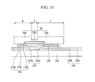
- FIG. 13 is a cross-sectional view of a thin film transistor array panel according to an exemplary embodiment of the present invention taken along line II-II of FIG. 1 .
- the cross-sectional structure of FIG. 13 is substantially similar to that of FIG. 2 , except for the source and drain electrodes 173 and 175 .
- a difference from the exemplary embodiment of FIG. 2 will be described.
- the data line 171 , the source electrode 173 , and the drain electrode 175 further include capping layers 171 r , 173 r , and 175 r formed on the main wiring layers 171 q , 173 q , and 175 q .
- the capping layers 171 r , 173 r , and 175 r include a metal oxide.
- the capping layers 171 r , 173 r , and 175 r may be formed of at least one of indium-zinc oxide, gallium-zinc oxide, aluminum-zinc oxide, and gallium-zinc oxide.
- the metal silicide layer 177 is formed only at lateral surfaces of the main wiring layers 171 q , 173 q , and 175 q .
- the lateral surfaces of the main wiring layers 171 q , 173 q and 175 q are not covered by the barrier layers 171 p , 173 p , and 175 p and the capping layers 171 r , 173 r , and 175 r .
- the lateral surface of the main wiring layers 171 q , 173 q and 175 q are exposed between the barrier layers 171 p , 173 p and 175 p and the capping layers 171 r , 173 r and 175 r.
- FIG. 2 may all be applied to the present exemplary embodiment of FIG. 13 .
- FIG. 14 to FIG. 20 are cross-sectional views showing a manufacturing method of a thin film transistor array panel according to an exemplary embodiment of the present invention.
- FIG. 14 to FIG. 20 sequentially show the cross-sectional views taken along line II-II of FIG. 1 .
- the manufacturing method of the thin film transistor array panel according to an exemplary embodiment of the present invention is substantially similar to the exemplary embodiment described in FIG. 4 to FIG. 9 .
- a metal oxide layer 170 r may be additionally formed on the metal layer 170 q .
- the metal oxide layer 170 r is patterned together with the underlying metal layer 170 q and the metal oxide layer 170 p , as shown in FIG. 17 , and thereby the capping layers 171 r , 173 r , and 175 r are formed on the main wiring layers 171 q , 173 q , and 175 q.
- the surfaces of the source electrode 173 and the drain electrode 175 are subjected to a silane (SiH 4 ) treatment to form a silane material layer 176 .
- the silane (SiH 4 ) treatment may be performed through a chemical vapor deposition (CVD) method.
- the silane material layer 176 is formed along the surface of the source electrode 173 and the drain electrode 175 that is treated with the silane (SiH 4 ). At this time, among each lateral surface of the source electrode 173 and the drain electrode 175 near the channel region positioned between the source electrode 173 and the drain electrode 175 , the silane material layer 176 is formed to cover the exposed lateral surfaces of the main wiring layers 171 q , 173 q , and 175 q between the barrier layers 171 p , 173 p , and 175 p and the capping layers 171 r , 173 r , and 175 r . The silane material layer 176 is formed to cover the channel region and the gate insulating layer 140 as well as the surface of the source electrode 173 and the drain electrode 175 .
- a passivation layer 180 is formed on the silane material layer 176 .
- the lower passivation layer 180 a containing a silicon oxide may be formed on the silane material layer 176 and the upper passivation layer 180 b containing silicon nitride may be formed on the lower passivation layer 180 a .
- the lower passivation layer 180 a including silicon oxide (SiO x ) may be formed by a reaction of silane (SiH 4 ) and nitrogen dioxide (NO 2 ).
- the silane material layer 176 and the main wiring layers 171 q , 173 q , and 175 q react with each other, thereby forming the metal silicide layer 177 .
- the main wiring layers 171 q , 173 q , and 175 q are formed of copper or the copper alloy.
- silicon of the silane material layer 176 may react with the copper or copper alloy at an interface between the silane material layer 176 and the source electrode 173 and the drain electrode 175 .
- the contact hole 185 exposing a part of the drain electrode 175 is formed by patterning the passivation layer 180 , and the pixel electrode 191 is formed on the passivation layer 180 to form the thin film transistor array panel of FIG. 13 .
- the pixel electrode 191 is formed to be physically connected with the drain electrode 175 through the contact hole 185 .
- FIG. 21 is the picture of an electronic microscope after the thin film transistor array panel according to an exemplary embodiment of the present invention is formed, and referring to FIG. 21 , the metal silicide layer 177 is uniformly formed at the interface between the main wiring layer 173 q and the lower passivation layer 180 a . Also, a pollution source such as a copper oxide is not formed.
Abstract
A thin film transistor array panel is provided as follows. A gate electrode is disposed on a substrate. A semiconductor layer is disposed on the gate electrode. A gate insulating layer is disposed between the gate electrode and the semiconductor layer. A source electrode is disposed on a first side of the semiconductor layer, having a first lateral surface. A drain electrode is disposed on a second side of the semiconductor layer, having a second lateral surface. The first and second lateral surfaces define a spacing which overlaps the gate electrode. A metal suicide layer is disposed on the first and second lateral surfaces. A passivation layer is disposed on the metal silicide layer, the source electrode and the drain electrode. The passivation layer is not in contact with the first and second lateral surfaces.
Description
This application is a divisional of U.S. application Ser. No. 14/466,317 filed on Aug. 22, 2014, which claims priority under 35 U.S.C. § 119 to Korean Patent Application No. 10-2014-0003548, filed on Jan. 10, 2014 in the Korean Intellectual Property Office, the disclosure of which is incorporated by reference herein in its entirety.
The present invention relates to a thin film transistor array panel and a manufacturing method thereof.
Displays such as a liquid crystal display (LCD), an organic light emitting diode (OLED) display, and the like include multiple pairs of electric field generating electrodes and an electro-optical active layer interposed therebetween. The liquid crystal display includes a liquid crystal layer as the electro-optical active layer, and the organic light emitting display includes an organic light emitting layer as the electro-optical active layer.
Field generating electrodes are connected to switching elements to receive electrical signals, and the electro-optical active layer converts the electrical signals into optical signals to display an image. Such switching elements include thin film transistors. The thin film transistors include a gate line transferring a scanning signal for controlling the thin film transistor, a data line transferring a signal applied to a pixel electrode.
As a displaying area of display devices becomes larger, faster propagation of the signals across the displaying area is required.
According to an exemplary embodiment of the present invention, a thin film transistor array panel is provided as follows. A gate electrode is disposed on a substrate. A semiconductor layer is disposed on the gate electrode. A gate insulating layer is disposed between the gate electrode and the semiconductor layer. A source electrode is disposed on a first side of the semiconductor layer, having a first lateral surface. A drain electrode is disposed on a second side of the semiconductor layer, having a second lateral surface. The first and second lateral surfaces define a spacing which overlaps the gate electrode. A metal silicide layer is disposed on the first and second lateral surfaces. A passivation layer is disposed on the metal silicide layer, the source electrode and the drain electrode. The passivation layer is not in contact with the first and second lateral surfaces.
According to an exemplary embodiment of the present invention, a method of manufacturing a thin film transistor array panel is provided as follows. A gate electrode is formed on a substrate. A semiconductor layer is formed on the substrate and the gate electrode. A gate insulating layer is formed between the gate electrode and the semiconductor layer. Source and drain electrodes are disposed on first and second sides of the gate electrode. The source and drain electrodes include a metal element. A silane (SiH4) material layer is formed on the source and drain electrodes. A passivation layer is formed on the source and drain electrodes. The forming of the passivation layer causes an silicidation process. The silicidation process includes a reaction between silicon of the silane (SiH4) material layer and the metal element of the source and drain electrodes thereby forming a metal silicide layer on first and second lateral sides of the source and drain electrodes. The first and second lateral sides define a spacing that overlaps the gate electrode. The first and second lateral sides are in contact with the metal silicide layer without being in contact with the passivation layer.
These and other features of the present invention will become more apparent by describing exemplary embodiments thereof with reference to the accompanying drawings of which:
Exemplary embodiments of the present invention will be described below in detail with reference to the accompanying drawings. However, the present invention may be embodied in different forms and should not be construed as limited to the embodiments set forth herein. In the drawings, the thickness of layers and regions may be exaggerated for clarity. It will also be understood that when an element is referred to as being “on” another element or substrate, it may be directly on the other element or substrate, or intervening layers may also be present. It will also be understood that when an element is referred to as being “coupled to” or “connected to” another element, it may be directly coupled to or connected to the other element, or intervening elements may also be present. Like reference numerals may refer to the like elements throughout the specification and drawings.
Referring to FIG. 1 and FIG. 2 , the thin film transistor array panel 100 includes gate lines 121 formed on an insulation substrate 110 formed of transparent glass or plastic.
The gate lines 121 transmit a gate signal and extend in a transverse direction. Each gate line 121 includes gate electrodes 124 protruding from the gate line 121.
The gate line 121 and the gate electrode 124 may have a dual-layer structure having first layers 121 p and 124 p and second layers 121 q and 124 q. Each of the first layers 121 p and 124 p and the second layers 121 q and 124 q may be formed of an aluminum-based metal such as aluminum (Al) and an aluminum alloy, a silver-based metal such as silver (Ag) and a silver alloy, a copper-based metal such as copper (Cu) and a copper alloy, a molybdenum-based metal such as molybdenum (Mo) and a molybdenum alloy, chromium (Cr), titanium (Ti), tantalum (Ta), manganese (Mn), or the like. For example, the first layers 121 p and 124 p may include titanium, and the second layers 121 q and 124 q may include copper or a copper alloy.
Alternatively, the first layers 121 p and 124 p and the second layers 121 q and the 124 q may be formed of a combination of films having different physical properties. The gate line 121 and the gate electrode 124 include two layers, but are not limited thereto, and may be formed as a single layer or three layers.
A gate insulating layer 140 formed of an insulating material such as a silicon oxide or a silicon nitride is positioned on the gate line 121. The gate insulating layer 140 may include a first insulating layer 140 a and a second insulating layer 140 b. The first insulating layer 140 a may be formed of a silicon nitride (SiNx) with a thickness of about 4000 Å, and the second insulating layer may be formed of a silicon oxide (SiOx) with a thickness of about 500 Å. Alternatively, the first insulating layer 140 a may be formed of a silicon oxynitride (SiON), and the second insulating layer 140 b may be formed of a silicon oxide (SiOx). The gate insulating layers 140 a and 140 b include two layers, but may include a single layer.
Semiconductor layers 151 are formed on the gate insulating layer 140. The semiconductor layers 151 may be formed of amorphous silicon, crystalline silicon, or an oxide semiconductor. The semiconductor layers 151 extend primarily in a vertical direction and include projections 154 that protrude toward the gate electrode 124.
When the semiconductor layer 151 is formed of an oxide semiconductor, the semiconductor layer 151 contains at least one of zinc (Zn), indium (In), tin (Sn), gallium (Ga), and hafnium (Hf). For example, The semiconductor layer 151 may be an indium-gallium-zinc oxide.
The drain electrode 175 is separated from the data line 171 and extends upward from the center of the “U” shape of the source electrode 173.
The data line 171, the source electrode 173, and the drain electrode 175 have a dual-film structure of barrier layers 171 p, 173 p, and 175 p and main wiring layers 171 q, 173 q, and 175 q. The barrier layers 171 p, 173 p, and 175 p are formed of a metal oxide and the main wiring layers 171 q, 173 q, and 175 q are formed of copper or the copper alloy.
For example, the barrier layers 171 p, 173 p, and 175 p may be formed of one of an indium-zinc oxide, a gallium-zinc oxide, and an aluminum-zinc oxide.
The barrier layers 171 p, 173 p, and 175 p serve to prevent the material such as copper or the like from being diffused to the semiconductor layer 151.
A metal silicide layer 177 is positioned on the main wiring layers 171 q, 173 q, and 175 q. The metal silicide layer 177 includes copper, silicon, and oxygen, and for example, may include a compound represented by CuSixOy. The metal silicide layer 177, covering the source electrode 173 and the drain electrode 175, is in contact with the surface of the source electrode 173 and the drain electrode 175. For example, the metal silicide layer 177 covers exposed lateral surfaces A and B of the source electrode 173 and the drain electrode 175 and exposed upper surfaces of the source electrode 173 and the drain electrode 175. The metal silicide layer 177 is not in contact with the gate insulating layer 140.
Hereafter, the exposed later surface A of the source electrode 173 and the drain electrode 175 near the channel region of the semiconductor layer 151 will be described.
Referring to FIG. 2 , the projection 154 of the semiconductor layer 151 includes a portion that is not covered by the data line 171, the source electrode 173 and the drain electrode 175. For example, the portion of the projection is exposed between the source electrode 173 and the drain electrode 175. The data line 151, the source electrode 173 and the drain electrode 175 are stacked on the semiconductor layer 151. The portion of the projection in the semiconductor layer 151 is exposed between the source and drain electrodes 173 and 175. The edge of the semiconductor layer 151 is vertically aligned with outer edges of the data line 171 and the drain electrode 175. Inner edges of the source and drain electrodes 173 and 175 defines the exposed portion of the projection 154. The edges of the data line 171, the source electrode 173 and the drain electrode 175 may be vertically sloped.
One gate electrode 124, one source electrode 173, and one drain electrode 175 form one thin film transistor (TFT) along with the projection 154 of the oxide semiconductor layer 151, and the channel of the thin film transistor is formed in the projection 154 between the source electrode 173 and the drain electrode 175.
Lateral surfaces of the source electrode 173 and the drain electrode 175 adjacent to the channel region are exposed, and exposed lateral parts A of the source electrode 173 and the drain electrode 175 are covered by the metal silicide layer 177. If the lateral parts A of the source electrode 173 and the drain electrode 175 is exposed without the metal silicide layer 177, if a following process forming the passivation layer including a silicon oxide is performed or a heat treatment to provide a channel characteristic to the protrusion 154 of the semiconductor layer is performed, the material such as copper included in the main wiring layers 171 q, 173 q, and 175 q forms an porous oxide such that the thin film transistor characteristic may be decreased.
Accordingly, the metal suicide layer may prevent the material such as copper or the like from being oxidized in performing subsequent processes such as forming the passivation layer and performing the heat treatment.
The metal suicide layer 177 may formed using two step processes including forming a silane material layer and performing a silicidation process using the silane material layer. Detailed descriptions will be made later with reference to FIGS. 8-10 . A passivation layer 180 is formed on the metal silicide layer 177. The passivation layer 180 is formed of an inorganic insulator such as a silicon nitride or a silicon oxide, an organic insulator, or a low-dielectric insulator.
The passivation layer 180 may include a lower passivation layer 180 a and an upper passivation layer 180 b. The lower passivation layer 180 a may be formed of a silicon oxide and the upper passivation layer 180 b may be formed of a silicon nitride.
Since the semiconductor layer 151 includes an oxide semiconductor, the lower passivation layer 180 a adjacent to the semiconductor layer 151 is formed of a silicon oxide. When the lower passivation layer 180 a is formed of a silicon nitride, the semiconductor layer 151 does not serve as a channel region of a thin film transistor.
The passivation layer 180 be in contact with the exposed part that is not covered by the source electrode 173 and the drain electrode 175 between the source electrode 173 and the drain electrode 175.
Contact holes 185 that expose one end of the drain electrodes 175 are formed on the passivation layer 180. Pixel electrodes 191 are formed on the passivation layer 180. The pixel electrode 191 is physically and electrically connected with the drain electrode 175 through the contact hole 185, and is applied with data voltage from the drain electrode 175.
The pixel electrode 191 may be formed of a transparent conductor such as ITO (Indium Tin Oxide) or IZO (Indium Zinc Oxide).
Referring to FIG. 3 , at least one of the molybdenum-based metal such as molybdenum (Mo) and the molybdenum alloy, the chromium-based metal such as chromium (Cr) and a chromium alloy, a titanium-based metal such as titanium (Ti) and a titanium alloy, a tantalum-based metal such as tantalum (Ta) and a tantalum alloy, and a manganese-based metal such as manganese (Mn) and a manganese alloy is deposited on the insulation substrate 110 formed of the transparent glass or plastic, and one selected from an aluminum-based metal such as aluminum and the aluminum alloy, a silver based-metal such as silver (Ag) and the silver alloy, and a copper-based metal such as copper (Cu) and the copper alloy is deposited thereon to form and pattern two layers, thereby forming the gate line 121 including the gate electrode 124. For example, the first layers 121 p and 124 p may contain titanium and the second layers 121 q and 124 q may contain copper or the copper alloy.
For example, after the two layers is formed, a photoresist (not illustrated) is deposited and patterned, and thereafter, the first layers 121 p and 124 p and the second layers 121 q and 124 q are etched together by using the patterned photoresist (not illustrated) as a mask. In this case, as an etchant, one that can etch both the first layers 121 p and 124 p and the second layers 121 q and 124 q may be used.
Referring to FIG. 4 , the gate insulating layer 140, an oxide layer 150, a metal oxide layer 170 p, and a metal layer 170 q are deposited on the gate line 121 and the gate electrode 124. In the gate insulating layer 140, the first insulating layer 140 a containing a silicon nitride may be deposited, and then the second insulating layer 140 b containing a silicon oxide may be deposited.
The oxide layer 150 may contain at least one of zinc (Zn), indium (In), tin (Sn), gallium (Ga), and hafnium (Hf), the metal oxide layer 170 p may contain one of an indium-zinc oxide, a gallium-zinc oxide, and an aluminum-zinc oxide, and the metal layer 170 q may contain copper or a copper alloy. A photoresist is formed and patterned to form a first photoresist pattern 50 thereon. The first photoresist pattern 50 has a thick first region 50 a and a relatively thin second region 50 b. A difference in thickness of the first photoresist pattern 50 may be formed by controlling the amount of irradiated light with a mask or by using a reflow method. When the amount of light is controlled, a slit pattern, a lattice pattern, or a semitransparent layer may be formed on the mask. The thin second region 50 b corresponds to a position where the channel region of the thin film transistor is to be formed.
Referring to FIG. 5 , the metal oxide layer 170 p and the metal layer 170 q are etched by using an etchant that may etch both the metal oxide layer 170 p and the metal layer 170 q by using the first photoresist pattern 50 as a mask. The etchant used herein may be the same as the etchant used when etching the first layers 121 p and 124 p and the second layers 121 q and 124 q of the gate line 121.
If the metal oxide layer 170 p and the metal layer 170 q are etched, lateral surfaces of the metal oxide layer 170 p and the metal layer 170 q covered with the first photoresist pattern 50 are also etched by the etchant, and as a result, a boundary line of the first metal layer 170 p and the second metal layer 170 q is positioned inside regions
A, B, and C where the first photoresist pattern 50 is formed.
In this case, the etchant that etches the metal oxide layer 170 p and the metal layer 170 q does not etch the gate insulating layer 140 and the oxide layer 150.
Additionally, the oxide layer 150 is etched by using the first photoresist pattern 50 as the mask.
Referring to FIG. 6 , the thin second region 50 b in FIG. 5 is removed by an etch-back process. In this case, the first region 50 a is also etched and thus decreased in width and height to become a second photoresist pattern 51 of FIG. 6 . The second photoresist pattern 51 is formed in regions B′ and C′ which are smaller than the regions B and C where the first photoresist pattern 50 is formed in FIG. 5 .
Referring to FIG. 7 , the metal oxide layer 170 p and the metal layer 170 q are etched with an etchant by using the second photoresist pattern 51 as a mask.
In this case, the metal oxide layer 170 p and the metal layer 170 q are patterned to form the data lines 171 p and 171 g, the source electrodes 173 p and 173 q, and the drain electrodes 175 p and 175 q having a two layered structure. Further, the oxide semiconductor layer 151 includes the projection 154. The projection 154 may serve as a channel region of a thin film transistor.
Using the photoresist patterns having different thicknesses, formed are the semiconductor layers 151 and 154, the barrier layers 171 p, 173 p, and 175 p, the main wiring layers 171 q, 173 q, and 175 q of the data line 171, the source electrode 173, and the drain electrode 175. Since the semiconductor layers 151 and 154, the data line 171, the source electrode 173, and the drain electrode 175 are formed using the photoresist patterns as an etch mask, edges of them are vertically aligned.
Next, referring to FIG. 8 , after the photoresist pattern is removed by an ashing process, the source electrode 173 and the drain electrode 175 are subjected to a silane (SiH4) treatment to form a silane material layer 176. The silane (SiH4) treatment may be performed through a chemical vapor deposition (CVD) process.
Referring to FIG. 9 , a silane material layer 176 is formed along the surface of the source electrode 173 and the drain electrode 175 that are treated with the silane (SiH4). At this time, each lateral surface of the source electrode 173 and the drain electrode 175 near the channel region positioned between the source electrode 173 and the drain electrode 175 is exposed, and the silane material layer 176 is formed on the exposed lateral surfaces of the source electrode and the drain electrode. For example, the exposed lateral surfaces of the source and drain electrodes are covered by the silane material layer 176.
The silane material layer 176 is formed to cover the channel region and the gate insulating layer 140 as well as the surface of the source electrode 173 and the drain electrode 175.
Referring to FIG. 10 , the passivation layer 180 is formed on the silane material layer 176. In forming the passivation layer 180, the lower passivation layer 180 a containing a silicon oxide may be formed on the silane material layer 176, and the upper passivation layer 180 b containing a silicon nitride may be formed on the lower passivation layer 180 a . The lower passivation layer 180 a including a silicon oxide (SiOx) may be formed by, for example, the reaction of SiH 4 and NO 2. In the process of the lower passivation layer 180 a, the silane material layer 176 may react with the copper or copper alloy of the main wiring layers 171 q , 173 q , and 175 q , thereby forming the metal silicide layer 177. Here, the silane material layer 176 may be selectively converted to the metal silicide layer 177 where the silane material layer 176 is in contact with the main wiring layers 171 q , 173 q , and 175 q formed of copper or the copper alloy.
The contact hole 185 exposing a part of the drain electrode 175 is formed by patterning the passivation layer 180, and the pixel electrode 191 is formed on the passivation layer 180 to form the thin film transistor array panel of FIG. 2 . In this case, the pixel electrode 191 is formed to be physically connected with the drain electrode 175 through the contact hole 185.
Referring to FIG. 11 , a second substrate 210 faces the insulation substrate 110. The second substrate 210 may be an insulation substrate formed of the transparent glass or plastic. A light blocking member 220 is formed on the second substrate 210. The light blocking member 220 may be formed of a black matrix and serve to prevent light leakage.
The light blocking member 220 and the color filter 230 are formed on an opposed array panel 200 as described above, however at least one of the light blocking member 220 and the color filter 230 may be formed on the thin film transistor array panel 100.
An overcoat 250 is formed on the color filter 230 and the light blocking member 220. The overcoat 250 may be formed of the insulation material. The overcoat 250 may seal the color filter 230, and may also provide a flat surface. Alternatively, the overcoat 250 may be omitted.
A common electrode 270 is formed on the overcoat 250.
The pixel electrode 191 applied with the data voltage generates an electric field together with the common electrode 270 applied with common voltage to determine a direction of liquid crystal molecules 31 of a liquid crystal layer 3 between the two electrodes. The pixel electrode 191 and the common electrode 270 constitute a capacitor to maintain the applied voltage even after the thin film transistor is turned off.
The pixel electrode 191 overlaps with a storage electrode line (not illustrated) to constitute a storage capacitor, and as a result, voltage storing capability of a liquid crystal capacitor may be increased.
The description of the thin film transistor array panel 100 may be applied with the content of the exemplary embodiment described with reference to FIG. 2 .
The thin film transistor array panel according to an exemplary embodiment is not limited to a liquid crystal display, but may be applied to other display systems such as an organic light emitting device.
Referring to FIG. 13 , the data line 171, the source electrode 173, and the drain electrode 175 further include capping layers 171 r, 173 r, and 175 r formed on the main wiring layers 171 q, 173 q, and 175 q. The capping layers 171 r, 173 r, and 175 r include a metal oxide. For example, the capping layers 171 r, 173 r, and 175 r may be formed of at least one of indium-zinc oxide, gallium-zinc oxide, aluminum-zinc oxide, and gallium-zinc oxide. For example, the metal silicide layer 177 is formed only at lateral surfaces of the main wiring layers 171 q, 173 q, and 175 q. The lateral surfaces of the main wiring layers 171 q, 173 q and 175 q are not covered by the barrier layers 171 p, 173 p, and 175 p and the capping layers 171 r, 173 r, and 175 r. For example, the lateral surface of the main wiring layers 171 q, 173 q and 175 q are exposed between the barrier layers 171 p, 173 p and 175 p and the capping layers 171 r, 173 r and 175 r.
Except for the described difference, the content described in FIG. 2 may all be applied to the present exemplary embodiment of FIG. 13 .
Referring to FIG. 14 to FIG. 19 , the manufacturing method of the thin film transistor array panel according to an exemplary embodiment of the present invention is substantially similar to the exemplary embodiment described in FIG. 4 to FIG. 9 . Referring to FIG. 14 , a metal oxide layer 170 r may be additionally formed on the metal layer 170 q. In following process, the metal oxide layer 170 r is patterned together with the underlying metal layer 170 q and the metal oxide layer 170 p, as shown in FIG. 17 , and thereby the capping layers 171 r, 173 r, and 175 r are formed on the main wiring layers 171 q, 173 q, and 175 q.
Referring to FIG. 18 , after the photoresist pattern is removed by an ashing process, the surfaces of the source electrode 173 and the drain electrode 175 are subjected to a silane (SiH4) treatment to form a silane material layer 176. The silane (SiH4) treatment may be performed through a chemical vapor deposition (CVD) method.
Referring to FIG. 19 , the silane material layer 176 is formed along the surface of the source electrode 173 and the drain electrode 175 that is treated with the silane (SiH4). At this time, among each lateral surface of the source electrode 173 and the drain electrode 175 near the channel region positioned between the source electrode 173 and the drain electrode 175, the silane material layer 176 is formed to cover the exposed lateral surfaces of the main wiring layers 171 q, 173 q, and 175 q between the barrier layers 171 p, 173 p, and 175 p and the capping layers 171 r, 173 r, and 175 r. The silane material layer 176 is formed to cover the channel region and the gate insulating layer 140 as well as the surface of the source electrode 173 and the drain electrode 175.
Referring to FIG. 20 , a passivation layer 180 is formed on the silane material layer 176. In forming the passivation layer 180, the lower passivation layer 180 a containing a silicon oxide may be formed on the silane material layer 176 and the upper passivation layer 180 b containing silicon nitride may be formed on the lower passivation layer 180 a. The lower passivation layer 180 a including silicon oxide (SiOx) may be formed by a reaction of silane (SiH4) and nitrogen dioxide (NO2). In the formation of the lower passivation layer 180 a, the silane material layer 176 and the main wiring layers 171 q, 173 q, and 175 q react with each other, thereby forming the metal silicide layer 177. The main wiring layers 171 q, 173 q, and 175 q are formed of copper or the copper alloy. In the formation of the lower passivation layer 180 a, silicon of the silane material layer 176 may react with the copper or copper alloy at an interface between the silane material layer 176 and the source electrode 173 and the drain electrode 175.
The contact hole 185 exposing a part of the drain electrode 175 is formed by patterning the passivation layer 180, and the pixel electrode 191 is formed on the passivation layer 180 to form the thin film transistor array panel of FIG. 13 . In this case, the pixel electrode 191 is formed to be physically connected with the drain electrode 175 through the contact hole 185.
While the present invention has been shown and described with reference to exemplary embodiments thereof, it will be apparent to those of ordinary skill in the art that various changes in form and detail may be made therein without departing from the spirit and scope of the present invention as defined by the following claims.
Claims (10)
1. A method of manufacturing a thin film transistor array panel, comprising:
forming a gate electrode on a substrate;
forming a semiconductor layer on the substrate and the gate electrode;
forming a gate insulating layer between the gate electrode and the semiconductor layer;
forming source and drain electrodes dispose d on first and second sides of the semiconductor layer, respectively, wherein the source and drain electrodes include a metal element;
forming a silane (SiH4) material layer on the source and drain electrodes; and
forming a passivation layer on the source and drain electrodes,
wherein the forming of the passivation layer causes a silicidation process wherein the silicidation process comprises a reaction between silicon of the silane (SiH4) material layer and the metal element of the source and drain electrodes thereby forming a metal silicide layer on first and second lateral sides of the source and drain electrodes, respectively, wherein the first and second lateral sides define a spacing that overlaps the gate electrode, wherein the first and second lateral sides are in direct with the metal silicide layer without being in contact with the passivation layer.
2. The method of claim 1 , wherein
the forming of the silane (SiH4) material layer is performed by a chemical vapor deposition process.
3. The method of claim 2 , wherein
the passivation layer is formed by a reaction of SiH4 and NO2.
4. The method of claim 3 , wherein
the passivation layer is in contact with the semiconductor layer through the spacing defined by the first and second lateral surfaces of the source and drain electrodes.
5. The method of claim 4 , wherein
the forming of the source electrode includes forming a barrier layer on the semiconductor layer and forming a main wiring layer on the barrier layer, and
the main wiring layer includes copper or a copper alloy and the barrier layer includes a metal oxide.
6. The method of claim 5 , wherein
the forming of the passivation layer includes forming a lower passivation layer and forming an upper passivation layer, wherein the forming of the lower passivation layer causes the silicidation process to occur at an interface between the main wiring layer and the silane (SiH4) material layer, wherein the lower passivation layer includes silicon oxide, and the upper passivation layer includes silicon nitride.
7. The method of claim 6 , wherein the metal silicide layer is further disposed on upper surfaces of the source and drain electrodes, wherein the upper surfaces of the source and drain electrodes are not in contact with the passivation layer.
8. The method of claim 5 , further comprising forming a capping layer on an upper surface of the main wiring layer, wherein the upper surface of the main wiring layer is not in contact with the passivation layer.
9. The method of claim 1 , wherein
the semiconductor layer includes an oxide semiconductor.
10. The method of claim 1 , wherein
the forming of the semiconductor layer and the forming of the source and drain electrodes are performed by using a mask.
Priority Applications (1)
| Application Number | Priority Date | Filing Date | Title |
|---|---|---|---|
| US15/343,780 US10032803B2 (en) | 2014-01-10 | 2016-11-04 | Thin film transistor array panel and method for manufacturing the same |
Applications Claiming Priority (4)
| Application Number | Priority Date | Filing Date | Title |
|---|---|---|---|
| KR1020140003548A KR102166898B1 (en) | 2014-01-10 | 2014-01-10 | Thin film transistor array panel and method for manufacturing the same |
| KR10-2014-0003548 | 2014-01-10 | ||
| US14/466,317 US9515093B2 (en) | 2014-01-10 | 2014-08-22 | Thin film transistor array panel and method for manufacturing the same |
| US15/343,780 US10032803B2 (en) | 2014-01-10 | 2016-11-04 | Thin film transistor array panel and method for manufacturing the same |
Related Parent Applications (1)
| Application Number | Title | Priority Date | Filing Date |
|---|---|---|---|
| US14/466,317 Division US9515093B2 (en) | 2014-01-10 | 2014-08-22 | Thin film transistor array panel and method for manufacturing the same |
Publications (2)
| Publication Number | Publication Date |
|---|---|
| US20170053940A1 US20170053940A1 (en) | 2017-02-23 |
| US10032803B2 true US10032803B2 (en) | 2018-07-24 |
Family
ID=53522008
Family Applications (2)
| Application Number | Title | Priority Date | Filing Date |
|---|---|---|---|
| US14/466,317 Active US9515093B2 (en) | 2014-01-10 | 2014-08-22 | Thin film transistor array panel and method for manufacturing the same |
| US15/343,780 Active US10032803B2 (en) | 2014-01-10 | 2016-11-04 | Thin film transistor array panel and method for manufacturing the same |
Family Applications Before (1)
| Application Number | Title | Priority Date | Filing Date |
|---|---|---|---|
| US14/466,317 Active US9515093B2 (en) | 2014-01-10 | 2014-08-22 | Thin film transistor array panel and method for manufacturing the same |
Country Status (4)
| Country | Link |
|---|---|
| US (2) | US9515093B2 (en) |
| JP (1) | JP2015133479A (en) |
| KR (1) | KR102166898B1 (en) |
| CN (1) | CN104779254A (en) |
Cited By (2)
| Publication number | Priority date | Publication date | Assignee | Title |
|---|---|---|---|---|
| US11037851B2 (en) | 2019-08-30 | 2021-06-15 | Applied Materials, Inc. | Nitrogen-rich silicon nitride films for thin film transistors |
| US11819847B2 (en) | 2020-07-20 | 2023-11-21 | Applied Materials, Inc. | Nanofluidic device with silicon nitride membrane |
Families Citing this family (17)
| Publication number | Priority date | Publication date | Assignee | Title |
|---|---|---|---|---|
| KR102166898B1 (en) | 2014-01-10 | 2020-10-19 | 삼성디스플레이 주식회사 | Thin film transistor array panel and method for manufacturing the same |
| WO2017045135A1 (en) | 2015-09-15 | 2017-03-23 | Boe Technology Group Co., Ltd. | Thin film transistor array substrate and fabrication method thereof, and display device |
| KR102618593B1 (en) * | 2015-12-29 | 2023-12-27 | 엘지디스플레이 주식회사 | Organic light emitting display and method of fabricating the same |
| US9576984B1 (en) * | 2016-01-14 | 2017-02-21 | Hon Hai Precision Industry Co., Ltd. | Thin film transistor array panel and conducting structure |
| US10734529B2 (en) * | 2016-01-29 | 2020-08-04 | Semiconductor Energy Laboratory Co., Ltd. | Semiconductor device and display device including the semiconductor device |
| CN205645818U (en) * | 2016-05-18 | 2016-10-12 | 武汉华星光电技术有限公司 | OLED (Organic light emitting diode) display panel |
| US10217771B2 (en) * | 2016-06-23 | 2019-02-26 | Samsung Display Co., Ltd. | Thin film transistor array panel and manufacturing method thereof |
| US10916430B2 (en) | 2016-07-25 | 2021-02-09 | Semiconductor Energy Laboratory Co., Ltd. | Semiconductor device and method for manufacturing the same |
| CN106206609B (en) * | 2016-08-17 | 2019-05-03 | 深圳市华星光电技术有限公司 | Display device plate and its manufacturing method |
| CN109360827A (en) * | 2018-08-23 | 2019-02-19 | 京东方科技集团股份有限公司 | Display base plate and its manufacturing method, display panel |
| CN108987418A (en) * | 2018-09-11 | 2018-12-11 | 惠科股份有限公司 | Array substrate and preparation method thereof and display device |
| KR20200054382A (en) * | 2018-11-09 | 2020-05-20 | 삼성디스플레이 주식회사 | Display panel |
| CN110223989A (en) * | 2019-05-28 | 2019-09-10 | 深圳市华星光电半导体显示技术有限公司 | Thin film transistor base plate and preparation method thereof |
| CN110648965A (en) * | 2019-10-23 | 2020-01-03 | 成都中电熊猫显示科技有限公司 | Array substrate manufacturing method and array substrate |
| CN110718561A (en) * | 2019-10-23 | 2020-01-21 | 成都中电熊猫显示科技有限公司 | Manufacturing method of array substrate and array substrate |
| CN111129104B (en) * | 2020-01-16 | 2023-04-07 | 深圳市华星光电半导体显示技术有限公司 | Display panel and display panel manufacturing method |
| US11444025B2 (en) * | 2020-06-18 | 2022-09-13 | Taiwan Semiconductor Manufacturing Company, Ltd. | Transistor and fabrication method thereof |
Citations (45)
| Publication number | Priority date | Publication date | Assignee | Title |
|---|---|---|---|---|
| US20020149016A1 (en) | 1998-07-16 | 2002-10-17 | Semiconductor Energy Laboratory Co., Ltd. | Semiconductor device with semiconductor circuit comprising semiconductior units, and method of fabricating it |
| US20040195573A1 (en) | 2003-04-04 | 2004-10-07 | Samsung Electronics Co., Ltd. | Liquid crystal display, thin film transistor array panel therefor, and manufacturing method thereof |
| US20050285233A1 (en) | 2004-06-24 | 2005-12-29 | Taiwan Semiconductor Manufacturing Co., Ltd. | Thin film transistor (TFT) device structure employing silicon rich silicon oxide passivation layer |
| US20060113549A1 (en) | 2004-11-10 | 2006-06-01 | Canon Kabushiki Kaisha | Light-emitting device |
| US7105868B2 (en) | 2002-06-24 | 2006-09-12 | Cermet, Inc. | High-electron mobility transistor with zinc oxide |
| US7211825B2 (en) | 2004-06-14 | 2007-05-01 | Yi-Chi Shih | Indium oxide-based thin film transistors and circuits |
| US20080068537A1 (en) | 2006-09-20 | 2008-03-20 | Samsung Electronics Co., Ltd. | Array substrate, display panel having the same and method of manufacturing the same |
| US20080296568A1 (en) | 2007-05-29 | 2008-12-04 | Samsung Electronics Co., Ltd | Thin film transistors and methods of manufacturing the same |
| US20080318368A1 (en) | 2007-06-20 | 2008-12-25 | Samsung Electronics Co., Ltd. | Method of manufacturing ZnO-based this film transistor |
| JP2009170769A (en) | 2008-01-18 | 2009-07-30 | Mitsubishi Materials Corp | Thin-film transistor |
| US20090218568A1 (en) * | 2008-03-01 | 2009-09-03 | Semiconductor Energy Laboratory Co., Ltd. | Thin film transisotr and display device |
| US20100051936A1 (en) * | 2006-12-05 | 2010-03-04 | Canon Kabushiki Kaisha | Bottom gate type thin film transistor, method of manufacturing the same, and display apparatus |
| US20100084648A1 (en) | 2007-04-09 | 2010-04-08 | Canon Kabushiki Kaisha | Light-emitting apparatus and production method thereof |
| US20100148176A1 (en) | 2008-12-15 | 2010-06-17 | Samsung Electronics Co., Ltd. | Thin film transistor display panel and manufacturing method thereof |
| US7790617B2 (en) | 2005-11-12 | 2010-09-07 | Chartered Semiconductor Manufacturing, Ltd. | Formation of metal silicide layer over copper interconnect for reliability enhancement |
| JP2011082380A (en) | 2009-10-08 | 2011-04-21 | Mitsubishi Electric Corp | Thin-film transistor and method of manufacturing the same |
| US20110175087A1 (en) * | 2010-01-20 | 2011-07-21 | Semiconductor Energy Laboratory Co., Ltd. | Semiconductor device |
| US20110193077A1 (en) * | 2010-02-05 | 2011-08-11 | Semiconductor Energy Laboratory Co., Ltd. | Semiconductor device and method for manufacturing the same |
| US20110227074A1 (en) * | 2010-03-19 | 2011-09-22 | Semiconductor Energy Laboratory Co., Ltd. | Semiconductor device |
| US20110242464A1 (en) | 2008-12-19 | 2011-10-06 | Sharp Kabushiki Kaisha | Insulated gate transistor, active matrix substrate, liquid crystal display device, and method for producing the same |
| US20110272699A1 (en) | 2004-11-26 | 2011-11-10 | Semiconductor Energy Laboratory Co., Ltd. | Method of manufacturing a semiconductor device |
| US20110298027A1 (en) * | 2010-06-04 | 2011-12-08 | Semiconductor Energy Laboratory Co., Ltd. | Semiconductor device |
| US20120068173A1 (en) * | 2006-08-31 | 2012-03-22 | Semiconductor Energy Laboratory Co., Ltd. | Liquid crystal display device |
| US20120074407A1 (en) * | 2010-02-12 | 2012-03-29 | Semiconductor Energy Laboratory Co., Ltd. | Semiconductor device and method for manufacturing the same |
| US20120097960A1 (en) | 1999-04-30 | 2012-04-26 | Semiconductor Energy Laboratory Co., Ltd. | Semiconductor device and manufacturing method thereof |
| US20120104385A1 (en) | 2010-11-03 | 2012-05-03 | Semiconductor Energy Laboratory Co., Ltd. | Semiconductor device |
| US20120119211A1 (en) * | 2010-11-17 | 2012-05-17 | Chimei Innolux Corporation | Thin film transistors and methods for manufacturing the same |
| US20120187410A1 (en) * | 2011-01-26 | 2012-07-26 | Semiconductor Energy Laboratory Co., Ltd. | Semiconductor device and manufacturing method thereof |
| US20120223300A1 (en) * | 2011-03-02 | 2012-09-06 | Samsung Electronics Co., Ltd. | Thin film transistor display panel and manufacturing method thereof |
| US20120223315A1 (en) | 2011-03-02 | 2012-09-06 | Hitachi Displays, Ltd. | Display device and manufacturing method of the same |
| US8313980B2 (en) | 2008-10-10 | 2012-11-20 | Semiconductor Energy Laboratory Co., Ltd. | Semiconductor device and manufacturing method thereof |
| KR20120138074A (en) | 2011-06-14 | 2012-12-24 | 삼성디스플레이 주식회사 | Thin film transistor, thin film transistor display panel and method of manufacturing the same |
| US20130001565A1 (en) * | 2011-07-01 | 2013-01-03 | Jung Sung-Woo | Display devices and methods of manufacturing display devices |
| US8389417B2 (en) | 2009-11-13 | 2013-03-05 | Semiconductor Energy Laboratory Co., Ltd. | Semiconductor device and manufacturing method thereof |
| US8410002B2 (en) | 2009-11-13 | 2013-04-02 | Semiconductor Energy Laboratory Co., Ltd. | Semiconductor device and manufacturing method thereof |
| JP2013103708A (en) | 2011-11-16 | 2013-05-30 | Hyundai Motor Co Ltd | Indoor temperature adjustment method of vehicle |
| US20130228756A1 (en) | 2012-03-05 | 2013-09-05 | Lg Display Co., Ltd. | Array Substrate and Method of Fabricating the Same |
| KR20130126240A (en) | 2012-05-11 | 2013-11-20 | 삼성디스플레이 주식회사 | Thin film transistor array panel |
| US20140151688A1 (en) * | 2012-12-03 | 2014-06-05 | Semiconductor Energy Laboratory Co., Ltd. | Semiconductor device |
| US20140240632A1 (en) * | 2008-02-15 | 2014-08-28 | Lg Display Co., Ltd. | Array substrate and liquid crystal display module including tft having improved mobility and method of fabricating the same |
| US20140284597A1 (en) * | 2013-03-19 | 2014-09-25 | Semiconductor Energy Laboratory Co., Ltd. | Oxide semiconductor film and method for forming oxide semiconductor film |
| US20140340608A1 (en) * | 2013-05-16 | 2014-11-20 | Semiconductor Energy Laboratory Co., Ltd. | Semiconductor device |
| US20150123118A1 (en) * | 2013-11-07 | 2015-05-07 | Lg Display Co., Ltd. | Array substrate and method of fabricating the same |
| US20150200212A1 (en) | 2014-01-10 | 2015-07-16 | Samsung Display Co., Ltd. | Thin film transistor array panel and method for manufacturing the same |
| US20160172383A1 (en) * | 2014-12-10 | 2016-06-16 | Semiconductor Energy Laboratory Co., Ltd. | Semiconductor Device and Driving Method Thereof |
Family Cites Families (7)
| Publication number | Priority date | Publication date | Assignee | Title |
|---|---|---|---|---|
| JP3347217B2 (en) * | 1994-04-22 | 2002-11-20 | 三菱電機株式会社 | Thin film transistor and method of manufacturing the same |
| JP2809196B2 (en) * | 1996-05-30 | 1998-10-08 | 日本電気株式会社 | Method for manufacturing semiconductor device |
| JP4955848B2 (en) * | 2000-02-28 | 2012-06-20 | エルジー ディスプレイ カンパニー リミテッド | Substrate manufacturing method for electronic device |
| KR101054344B1 (en) * | 2004-11-17 | 2011-08-04 | 삼성전자주식회사 | Thin film transistor array panel and manufacturing method thereof |
| JP5284978B2 (en) * | 2007-11-14 | 2013-09-11 | パナソニック株式会社 | Thin film transistor manufacturing method |
| EP2065927B1 (en) * | 2007-11-27 | 2013-10-02 | Imec | Integration and manufacturing method of Cu germanide and Cu silicide as Cu capping layer |
| KR20110133251A (en) * | 2010-06-04 | 2011-12-12 | 삼성전자주식회사 | Thin film transistor array panel and manufacturing method of the same |
-
2014
- 2014-01-10 KR KR1020140003548A patent/KR102166898B1/en active IP Right Grant
- 2014-08-22 US US14/466,317 patent/US9515093B2/en active Active
- 2014-12-02 JP JP2014244005A patent/JP2015133479A/en active Pending
- 2014-12-31 CN CN201410850991.2A patent/CN104779254A/en active Pending
-
2016
- 2016-11-04 US US15/343,780 patent/US10032803B2/en active Active
Patent Citations (46)
| Publication number | Priority date | Publication date | Assignee | Title |
|---|---|---|---|---|
| US20020149016A1 (en) | 1998-07-16 | 2002-10-17 | Semiconductor Energy Laboratory Co., Ltd. | Semiconductor device with semiconductor circuit comprising semiconductior units, and method of fabricating it |
| US20120097960A1 (en) | 1999-04-30 | 2012-04-26 | Semiconductor Energy Laboratory Co., Ltd. | Semiconductor device and manufacturing method thereof |
| US7105868B2 (en) | 2002-06-24 | 2006-09-12 | Cermet, Inc. | High-electron mobility transistor with zinc oxide |
| US20040195573A1 (en) | 2003-04-04 | 2004-10-07 | Samsung Electronics Co., Ltd. | Liquid crystal display, thin film transistor array panel therefor, and manufacturing method thereof |
| US7211825B2 (en) | 2004-06-14 | 2007-05-01 | Yi-Chi Shih | Indium oxide-based thin film transistors and circuits |
| US20050285233A1 (en) | 2004-06-24 | 2005-12-29 | Taiwan Semiconductor Manufacturing Co., Ltd. | Thin film transistor (TFT) device structure employing silicon rich silicon oxide passivation layer |
| US20060113549A1 (en) | 2004-11-10 | 2006-06-01 | Canon Kabushiki Kaisha | Light-emitting device |
| US20110272699A1 (en) | 2004-11-26 | 2011-11-10 | Semiconductor Energy Laboratory Co., Ltd. | Method of manufacturing a semiconductor device |
| US7790617B2 (en) | 2005-11-12 | 2010-09-07 | Chartered Semiconductor Manufacturing, Ltd. | Formation of metal silicide layer over copper interconnect for reliability enhancement |
| US20120068173A1 (en) * | 2006-08-31 | 2012-03-22 | Semiconductor Energy Laboratory Co., Ltd. | Liquid crystal display device |
| US20080068537A1 (en) | 2006-09-20 | 2008-03-20 | Samsung Electronics Co., Ltd. | Array substrate, display panel having the same and method of manufacturing the same |
| US20100051936A1 (en) * | 2006-12-05 | 2010-03-04 | Canon Kabushiki Kaisha | Bottom gate type thin film transistor, method of manufacturing the same, and display apparatus |
| US20100084648A1 (en) | 2007-04-09 | 2010-04-08 | Canon Kabushiki Kaisha | Light-emitting apparatus and production method thereof |
| US20080296568A1 (en) | 2007-05-29 | 2008-12-04 | Samsung Electronics Co., Ltd | Thin film transistors and methods of manufacturing the same |
| US20080318368A1 (en) | 2007-06-20 | 2008-12-25 | Samsung Electronics Co., Ltd. | Method of manufacturing ZnO-based this film transistor |
| JP2009170769A (en) | 2008-01-18 | 2009-07-30 | Mitsubishi Materials Corp | Thin-film transistor |
| US20140240632A1 (en) * | 2008-02-15 | 2014-08-28 | Lg Display Co., Ltd. | Array substrate and liquid crystal display module including tft having improved mobility and method of fabricating the same |
| US20090218568A1 (en) * | 2008-03-01 | 2009-09-03 | Semiconductor Energy Laboratory Co., Ltd. | Thin film transisotr and display device |
| US8313980B2 (en) | 2008-10-10 | 2012-11-20 | Semiconductor Energy Laboratory Co., Ltd. | Semiconductor device and manufacturing method thereof |
| US20100148176A1 (en) | 2008-12-15 | 2010-06-17 | Samsung Electronics Co., Ltd. | Thin film transistor display panel and manufacturing method thereof |
| US20110242464A1 (en) | 2008-12-19 | 2011-10-06 | Sharp Kabushiki Kaisha | Insulated gate transistor, active matrix substrate, liquid crystal display device, and method for producing the same |
| JP2011082380A (en) | 2009-10-08 | 2011-04-21 | Mitsubishi Electric Corp | Thin-film transistor and method of manufacturing the same |
| US8389417B2 (en) | 2009-11-13 | 2013-03-05 | Semiconductor Energy Laboratory Co., Ltd. | Semiconductor device and manufacturing method thereof |
| US8410002B2 (en) | 2009-11-13 | 2013-04-02 | Semiconductor Energy Laboratory Co., Ltd. | Semiconductor device and manufacturing method thereof |
| US20110175087A1 (en) * | 2010-01-20 | 2011-07-21 | Semiconductor Energy Laboratory Co., Ltd. | Semiconductor device |
| WO2011096263A1 (en) | 2010-02-05 | 2011-08-11 | Semiconductor Energy Laboratory Co., Ltd. | Semiconductor device and method for manufacturing the same |
| US20110193077A1 (en) * | 2010-02-05 | 2011-08-11 | Semiconductor Energy Laboratory Co., Ltd. | Semiconductor device and method for manufacturing the same |
| US20120074407A1 (en) * | 2010-02-12 | 2012-03-29 | Semiconductor Energy Laboratory Co., Ltd. | Semiconductor device and method for manufacturing the same |
| US20110227074A1 (en) * | 2010-03-19 | 2011-09-22 | Semiconductor Energy Laboratory Co., Ltd. | Semiconductor device |
| US20110298027A1 (en) * | 2010-06-04 | 2011-12-08 | Semiconductor Energy Laboratory Co., Ltd. | Semiconductor device |
| US20120104385A1 (en) | 2010-11-03 | 2012-05-03 | Semiconductor Energy Laboratory Co., Ltd. | Semiconductor device |
| US20120119211A1 (en) * | 2010-11-17 | 2012-05-17 | Chimei Innolux Corporation | Thin film transistors and methods for manufacturing the same |
| US20120187410A1 (en) * | 2011-01-26 | 2012-07-26 | Semiconductor Energy Laboratory Co., Ltd. | Semiconductor device and manufacturing method thereof |
| US20120223300A1 (en) * | 2011-03-02 | 2012-09-06 | Samsung Electronics Co., Ltd. | Thin film transistor display panel and manufacturing method thereof |
| US20120223315A1 (en) | 2011-03-02 | 2012-09-06 | Hitachi Displays, Ltd. | Display device and manufacturing method of the same |
| KR20120138074A (en) | 2011-06-14 | 2012-12-24 | 삼성디스플레이 주식회사 | Thin film transistor, thin film transistor display panel and method of manufacturing the same |
| US20130001565A1 (en) * | 2011-07-01 | 2013-01-03 | Jung Sung-Woo | Display devices and methods of manufacturing display devices |
| JP2013103708A (en) | 2011-11-16 | 2013-05-30 | Hyundai Motor Co Ltd | Indoor temperature adjustment method of vehicle |
| US20130228756A1 (en) | 2012-03-05 | 2013-09-05 | Lg Display Co., Ltd. | Array Substrate and Method of Fabricating the Same |
| KR20130126240A (en) | 2012-05-11 | 2013-11-20 | 삼성디스플레이 주식회사 | Thin film transistor array panel |
| US20140151688A1 (en) * | 2012-12-03 | 2014-06-05 | Semiconductor Energy Laboratory Co., Ltd. | Semiconductor device |
| US20140284597A1 (en) * | 2013-03-19 | 2014-09-25 | Semiconductor Energy Laboratory Co., Ltd. | Oxide semiconductor film and method for forming oxide semiconductor film |
| US20140340608A1 (en) * | 2013-05-16 | 2014-11-20 | Semiconductor Energy Laboratory Co., Ltd. | Semiconductor device |
| US20150123118A1 (en) * | 2013-11-07 | 2015-05-07 | Lg Display Co., Ltd. | Array substrate and method of fabricating the same |
| US20150200212A1 (en) | 2014-01-10 | 2015-07-16 | Samsung Display Co., Ltd. | Thin film transistor array panel and method for manufacturing the same |
| US20160172383A1 (en) * | 2014-12-10 | 2016-06-16 | Semiconductor Energy Laboratory Co., Ltd. | Semiconductor Device and Driving Method Thereof |
Cited By (3)
| Publication number | Priority date | Publication date | Assignee | Title |
|---|---|---|---|---|
| US11037851B2 (en) | 2019-08-30 | 2021-06-15 | Applied Materials, Inc. | Nitrogen-rich silicon nitride films for thin film transistors |
| US11699628B2 (en) | 2019-08-30 | 2023-07-11 | Applied Materials, Inc. | Nitrogen-rich silicon nitride films for thin film transistors |
| US11819847B2 (en) | 2020-07-20 | 2023-11-21 | Applied Materials, Inc. | Nanofluidic device with silicon nitride membrane |
Also Published As
| Publication number | Publication date |
|---|---|
| US20150200212A1 (en) | 2015-07-16 |
| US9515093B2 (en) | 2016-12-06 |
| JP2015133479A (en) | 2015-07-23 |
| KR20150083693A (en) | 2015-07-20 |
| US20170053940A1 (en) | 2017-02-23 |
| KR102166898B1 (en) | 2020-10-19 |
| CN104779254A (en) | 2015-07-15 |
Similar Documents
| Publication | Publication Date | Title |
|---|---|---|
| US10032803B2 (en) | Thin film transistor array panel and method for manufacturing the same | |
| US9437618B2 (en) | Pixel structure and method of fabricating the same | |
| US8957418B2 (en) | Semiconductor device and display apparatus | |
| KR102281846B1 (en) | Thin film transistor array panel and method of manufacturing the same | |
| KR102131195B1 (en) | Display substrate having a thin film transistor and method of manufacturing the same | |
| US11177293B2 (en) | Array substrate and fabricating method thereof, and display device | |
| KR102169684B1 (en) | Thin film transistor array panel and method for manufacturing the same | |
| US9281322B2 (en) | Thin film transistor array panel and method for manufacturing the same | |
| KR102494732B1 (en) | Thin film transistor array panel and method for manufacturing the same | |
| KR20140081412A (en) | Thin film transistor array panel and method for manufacturing the same | |
| KR20140083136A (en) | Thin film transistor array panel and method of manufacturing the same | |
| JP5991668B2 (en) | Display device and manufacturing method thereof | |
| WO2018061954A1 (en) | Thin film transistor substrate, manufacturing method for thin film transistor substrate, and display device | |
| US8618538B2 (en) | Thin film transistor array panel and manufacturing method thereof | |
| US10115745B2 (en) | TFT array substrate and method of forming the same | |
| KR102338190B1 (en) | Thin film transistor array panel, liquid crystal display including the same, and method manufacturing the panel | |
| KR20160119314A (en) | Thin film transistor array panel, liquid crystal display and manufacturing method thereof | |
| KR20160129160A (en) | Thin film transistor array panel and method of manufacturing the same | |
| JP6255452B2 (en) | Display device and manufacturing method thereof | |
| KR20150111550A (en) | Thin film transistor array panel and method of manufacturing the same | |
| KR101707039B1 (en) | Display substrate | |
| US20160204135A1 (en) | Thin film transistor array panel and method for manufacturing the same |
Legal Events
| Date | Code | Title | Description |
|---|---|---|---|
| STCF | Information on status: patent grant |
Free format text: PATENTED CASE |
|
| MAFP | Maintenance fee payment |
Free format text: PAYMENT OF MAINTENANCE FEE, 4TH YEAR, LARGE ENTITY (ORIGINAL EVENT CODE: M1551); ENTITY STATUS OF PATENT OWNER: LARGE ENTITY Year of fee payment: 4 |