US10026914B2 - Organic light emitting device and method for fabricating the same, and display apparatus - Google Patents
Organic light emitting device and method for fabricating the same, and display apparatus Download PDFInfo
- Publication number
- US10026914B2 US10026914B2 US15/512,099 US201615512099A US10026914B2 US 10026914 B2 US10026914 B2 US 10026914B2 US 201615512099 A US201615512099 A US 201615512099A US 10026914 B2 US10026914 B2 US 10026914B2
- Authority
- US
- United States
- Prior art keywords
- layer
- light emitting
- doped layer
- organic light
- emitting device
- Prior art date
- Legal status (The legal status is an assumption and is not a legal conclusion. Google has not performed a legal analysis and makes no representation as to the accuracy of the status listed.)
- Active
Links
- 238000000034 method Methods 0.000 title claims abstract description 89
- 239000010410 layer Substances 0.000 claims abstract description 252
- 239000002346 layers by function Substances 0.000 claims abstract description 23
- 238000002347 injection Methods 0.000 claims description 29
- 239000007924 injection Substances 0.000 claims description 29
- 238000000576 coating method Methods 0.000 claims description 24
- 239000000463 material Substances 0.000 claims description 19
- 230000005525 hole transport Effects 0.000 claims description 13
- 239000000758 substrate Substances 0.000 claims description 13
- 238000002207 thermal evaporation Methods 0.000 claims description 13
- 238000004528 spin coating Methods 0.000 claims description 8
- 238000003618 dip coating Methods 0.000 claims description 6
- 238000007641 inkjet printing Methods 0.000 claims description 6
- 238000007644 letterpress printing Methods 0.000 claims description 6
- 238000007639 printing Methods 0.000 claims description 6
- 230000005855 radiation Effects 0.000 claims description 6
- 238000000859 sublimation Methods 0.000 claims description 6
- 230000008022 sublimation Effects 0.000 claims description 6
- 238000010345 tape casting Methods 0.000 claims description 6
- 238000001931 thermography Methods 0.000 claims description 6
- 238000010023 transfer printing Methods 0.000 claims description 6
- 238000007740 vapor deposition Methods 0.000 claims description 6
- 239000000243 solution Substances 0.000 description 13
- 239000002019 doping agent Substances 0.000 description 9
- 239000011521 glass Substances 0.000 description 7
- 238000010586 diagram Methods 0.000 description 6
- 230000008020 evaporation Effects 0.000 description 6
- 238000001704 evaporation Methods 0.000 description 6
- UEEXRMUCXBPYOV-UHFFFAOYSA-N iridium;2-phenylpyridine Chemical compound [Ir].C1=CC=CC=C1C1=CC=CC=N1.C1=CC=CC=C1C1=CC=CC=N1.C1=CC=CC=C1C1=CC=CC=N1 UEEXRMUCXBPYOV-UHFFFAOYSA-N 0.000 description 5
- PQXKHYXIUOZZFA-UHFFFAOYSA-M lithium fluoride Chemical compound [Li+].[F-] PQXKHYXIUOZZFA-UHFFFAOYSA-M 0.000 description 5
- 229920003227 poly(N-vinyl carbazole) Polymers 0.000 description 5
- CSCPPACGZOOCGX-UHFFFAOYSA-N Acetone Chemical compound CC(C)=O CSCPPACGZOOCGX-UHFFFAOYSA-N 0.000 description 4
- IJGRMHOSHXDMSA-UHFFFAOYSA-N Atomic nitrogen Chemical compound N#N IJGRMHOSHXDMSA-UHFFFAOYSA-N 0.000 description 4
- HNWFFTUWRIGBNM-UHFFFAOYSA-N 2-methyl-9,10-dinaphthalen-2-ylanthracene Chemical compound C1=CC=CC2=CC(C3=C4C=CC=CC4=C(C=4C=C5C=CC=CC5=CC=4)C4=CC=C(C=C43)C)=CC=C21 HNWFFTUWRIGBNM-UHFFFAOYSA-N 0.000 description 3
- 229920000144 PEDOT:PSS Polymers 0.000 description 3
- 230000002950 deficient Effects 0.000 description 3
- 229920002098 polyfluorene Polymers 0.000 description 3
- DHDHJYNTEFLIHY-UHFFFAOYSA-N 4,7-diphenyl-1,10-phenanthroline Chemical compound C1=CC=CC=C1C1=CC=NC2=C1C=CC1=C(C=3C=CC=CC=3)C=CN=C21 DHDHJYNTEFLIHY-UHFFFAOYSA-N 0.000 description 2
- LFQSCWFLJHTTHZ-UHFFFAOYSA-N Ethanol Chemical compound CCO LFQSCWFLJHTTHZ-UHFFFAOYSA-N 0.000 description 2
- 229920001609 Poly(3,4-ethylenedioxythiophene) Polymers 0.000 description 2
- QVGXLLKOCUKJST-UHFFFAOYSA-N atomic oxygen Chemical compound [O] QVGXLLKOCUKJST-UHFFFAOYSA-N 0.000 description 2
- 239000008367 deionised water Substances 0.000 description 2
- 229910021641 deionized water Inorganic materials 0.000 description 2
- 238000000151 deposition Methods 0.000 description 2
- 230000000694 effects Effects 0.000 description 2
- 229910052751 metal Inorganic materials 0.000 description 2
- 239000002184 metal Substances 0.000 description 2
- ONFSYSWBTGIEQE-NBHCHVEOSA-N n,n-diphenyl-4-[(e)-2-[4-[(e)-2-[4-(n-phenylanilino)phenyl]ethenyl]phenyl]ethenyl]aniline Chemical compound C=1C=C(\C=C\C=2C=CC(=CC=2)N(C=2C=CC=CC=2)C=2C=CC=CC=2)C=CC=1/C=C/C(C=C1)=CC=C1N(C=1C=CC=CC=1)C1=CC=CC=C1 ONFSYSWBTGIEQE-NBHCHVEOSA-N 0.000 description 2
- 229910052757 nitrogen Inorganic materials 0.000 description 2
- 239000001301 oxygen Substances 0.000 description 2
- 229910052760 oxygen Inorganic materials 0.000 description 2
- 210000002381 plasma Anatomy 0.000 description 2
- 229920001467 poly(styrenesulfonates) Polymers 0.000 description 2
- XLYOFNOQVPJJNP-UHFFFAOYSA-N water Chemical compound O XLYOFNOQVPJJNP-UHFFFAOYSA-N 0.000 description 2
- 229910052782 aluminium Inorganic materials 0.000 description 1
- XAGFODPZIPBFFR-UHFFFAOYSA-N aluminium Chemical compound [Al] XAGFODPZIPBFFR-UHFFFAOYSA-N 0.000 description 1
- 230000015572 biosynthetic process Effects 0.000 description 1
- 230000000052 comparative effect Effects 0.000 description 1
- 238000005516 engineering process Methods 0.000 description 1
- 238000005530 etching Methods 0.000 description 1
- AMGQUBHHOARCQH-UHFFFAOYSA-N indium;oxotin Chemical compound [In].[Sn]=O AMGQUBHHOARCQH-UHFFFAOYSA-N 0.000 description 1
- 238000012986 modification Methods 0.000 description 1
- 230000004048 modification Effects 0.000 description 1
- 230000027756 respiratory electron transport chain Effects 0.000 description 1
- 239000004065 semiconductor Substances 0.000 description 1
- 238000001228 spectrum Methods 0.000 description 1
- 238000006467 substitution reaction Methods 0.000 description 1
Images


Classifications
-
- H—ELECTRICITY
- H10—SEMICONDUCTOR DEVICES; ELECTRIC SOLID-STATE DEVICES NOT OTHERWISE PROVIDED FOR
- H10K—ORGANIC ELECTRIC SOLID-STATE DEVICES
- H10K50/00—Organic light-emitting devices
- H10K50/10—OLEDs or polymer light-emitting diodes [PLED]
- H10K50/11—OLEDs or polymer light-emitting diodes [PLED] characterised by the electroluminescent [EL] layers
- H10K50/12—OLEDs or polymer light-emitting diodes [PLED] characterised by the electroluminescent [EL] layers comprising dopants
-
- H—ELECTRICITY
- H10—SEMICONDUCTOR DEVICES; ELECTRIC SOLID-STATE DEVICES NOT OTHERWISE PROVIDED FOR
- H10K—ORGANIC ELECTRIC SOLID-STATE DEVICES
- H10K71/00—Manufacture or treatment specially adapted for the organic devices covered by this subclass
- H10K71/10—Deposition of organic active material
- H10K71/12—Deposition of organic active material using liquid deposition, e.g. spin coating
-
- H01L51/5024—
-
- H01L51/0003—
-
- H01L51/0008—
-
- H01L51/0013—
-
- H01L51/56—
-
- H—ELECTRICITY
- H10—SEMICONDUCTOR DEVICES; ELECTRIC SOLID-STATE DEVICES NOT OTHERWISE PROVIDED FOR
- H10K—ORGANIC ELECTRIC SOLID-STATE DEVICES
- H10K50/00—Organic light-emitting devices
- H10K50/10—OLEDs or polymer light-emitting diodes [PLED]
- H10K50/11—OLEDs or polymer light-emitting diodes [PLED] characterised by the electroluminescent [EL] layers
- H10K50/125—OLEDs or polymer light-emitting diodes [PLED] characterised by the electroluminescent [EL] layers specially adapted for multicolour light emission, e.g. for emitting white light
- H10K50/13—OLEDs or polymer light-emitting diodes [PLED] characterised by the electroluminescent [EL] layers specially adapted for multicolour light emission, e.g. for emitting white light comprising stacked EL layers within one EL unit
-
- H—ELECTRICITY
- H10—SEMICONDUCTOR DEVICES; ELECTRIC SOLID-STATE DEVICES NOT OTHERWISE PROVIDED FOR
- H10K—ORGANIC ELECTRIC SOLID-STATE DEVICES
- H10K50/00—Organic light-emitting devices
- H10K50/10—OLEDs or polymer light-emitting diodes [PLED]
- H10K50/14—Carrier transporting layers
- H10K50/15—Hole transporting layers
- H10K50/156—Hole transporting layers comprising a multilayered structure
-
- H—ELECTRICITY
- H10—SEMICONDUCTOR DEVICES; ELECTRIC SOLID-STATE DEVICES NOT OTHERWISE PROVIDED FOR
- H10K—ORGANIC ELECTRIC SOLID-STATE DEVICES
- H10K71/00—Manufacture or treatment specially adapted for the organic devices covered by this subclass
-
- H—ELECTRICITY
- H10—SEMICONDUCTOR DEVICES; ELECTRIC SOLID-STATE DEVICES NOT OTHERWISE PROVIDED FOR
- H10K—ORGANIC ELECTRIC SOLID-STATE DEVICES
- H10K71/00—Manufacture or treatment specially adapted for the organic devices covered by this subclass
- H10K71/10—Deposition of organic active material
- H10K71/16—Deposition of organic active material using physical vapour deposition [PVD], e.g. vacuum deposition or sputtering
- H10K71/164—Deposition of organic active material using physical vapour deposition [PVD], e.g. vacuum deposition or sputtering using vacuum deposition
-
- H—ELECTRICITY
- H10—SEMICONDUCTOR DEVICES; ELECTRIC SOLID-STATE DEVICES NOT OTHERWISE PROVIDED FOR
- H10K—ORGANIC ELECTRIC SOLID-STATE DEVICES
- H10K71/00—Manufacture or treatment specially adapted for the organic devices covered by this subclass
- H10K71/10—Deposition of organic active material
- H10K71/18—Deposition of organic active material using non-liquid printing techniques, e.g. thermal transfer printing from a donor sheet
-
- H—ELECTRICITY
- H10—SEMICONDUCTOR DEVICES; ELECTRIC SOLID-STATE DEVICES NOT OTHERWISE PROVIDED FOR
- H10K—ORGANIC ELECTRIC SOLID-STATE DEVICES
- H10K71/00—Manufacture or treatment specially adapted for the organic devices covered by this subclass
- H10K71/30—Doping active layers, e.g. electron transporting layers
-
- H—ELECTRICITY
- H10—SEMICONDUCTOR DEVICES; ELECTRIC SOLID-STATE DEVICES NOT OTHERWISE PROVIDED FOR
- H10K—ORGANIC ELECTRIC SOLID-STATE DEVICES
- H10K2101/00—Properties of the organic materials covered by group H10K85/00
- H10K2101/10—Triplet emission
-
- H—ELECTRICITY
- H10—SEMICONDUCTOR DEVICES; ELECTRIC SOLID-STATE DEVICES NOT OTHERWISE PROVIDED FOR
- H10K—ORGANIC ELECTRIC SOLID-STATE DEVICES
- H10K50/00—Organic light-emitting devices
- H10K50/10—OLEDs or polymer light-emitting diodes [PLED]
- H10K50/11—OLEDs or polymer light-emitting diodes [PLED] characterised by the electroluminescent [EL] layers
Definitions
- the embodiments of the present disclosure relate to the field of semiconductor fabricating technologies, and particularly, to an organic light emitting device and a method for fabricating the same, and a display apparatus.
- the current solution process can fabricate green and red light devices with excellent performances, but there is still a large gap between such fabricated blue light device and the VTE-fabricated blue light device in efficiency or in lifetime.
- an Open Mask is usually adopted to fabricate the blue light common layer.
- This functional layer serves as an electron transfer layer in the red and green subpixels without emitting light, while acts as a blue light emitting layer in the blue subpixels.
- both sides of an interface between the blue light emitting layer and the solution process light emitting layer are doped layers, and the process modes of the first and second doped layers are different from each other, which will easily cause the problems such as efficiency decrease.
- the process modes of the first and second doped layers are different from each other, which will easily cause the problems such as efficiency decrease.
- such an interface is not efficiently improved, and thus the performance of the OLED is certainly affected.
- the embodiments of the present disclosure provide an organic light emitting device and a method for fabricating the same, and a display apparatus, which are capable of improving the problem of a defective heterogeneous interface, thereby extending the lifespan of the OLED, reducing the operating voltage and improving the efficiency.
- a first aspect of the embodiments of the present disclosure provides an organic light emitting device including a first electrode, a second electrode, and an organic functional layer, wherein the organic functional layer includes a first doped layer fabricated in a first process, a second doped layer fabricated in a second process, and an auxiliary layer formed between the first doped layer and the second doped layer.
- the material of the auxiliary layer is the same as the body material of the second doped layer, and the auxiliary layer is used to improve the performance of the first doped layer.
- the auxiliary layer has an electron mobility more than 1 ⁇ 10 ⁇ 4 m 2 /V*s (square meters per volt seconds).
- the auxiliary layer has a thickness ranging from 1 nm to 5 nm.
- the auxiliary layer is fabricated in the second process.
- the first doped layer includes an organic light emitting layer
- the second doped layer includes a blue light common layer.
- the first process is selected from one or any combination of a spin-coating method, a knife coating method, an electrospray coating method, a slit coating method, a strip coating method, a dip coating method, a drum coating method, an ink-jet printing method, a nozzle printing method, and a letterpress printing method.
- the second process is selected from one or any combination of a vacuum thermal evaporation, an organic vapor deposition, a laser-induced thermal imaging, and a radiation-induced sublimation transfer printing.
- the organic functional layer further includes a hole injection layer, a hole transport layer, an electron transport layer, and an electron injection layer.
- a second aspect of the embodiments of the present disclosure provides a method for fabricating an organic light emitting device including sequentially forming a first electrode, an organic functional layer and a second electrode on a substrate, wherein, forming the organic functional layer includes fabricating a first doped layer in a first process, forming an auxiliary layer on the first doped layer, and fabricating a second doped layer on the auxiliary layer in a second process.
- the material of the auxiliary layer is the same as the body material of the second doped layer, and the auxiliary layer is used to improve the performance of the first doped layer.
- the auxiliary layer has an electron mobility more than 1 ⁇ 10 ⁇ 4 m 2 /V*s.
- the auxiliary layer has a thickness ranging from 1 nm to 5 nm.
- forming the auxiliary layer includes fabricating the auxiliary layer in the second process.
- the first doped layer includes an organic light emitting layer
- the second doped layer includes a blue light common layer.
- the first process is selected from one or any combination of a spin-coating method, a knife coating method, an electrospray coating method, a slit coating method, a strip coating method, a dip coating method, a drum coating method, an ink-jet printing method, a nozzle printing method, and a letterpress printing method.
- the second process is selected from one or any combination of a vacuum thermal evaporation, an organic vapor deposition, a laser-induced thermal imaging, and a radiation-induced sublimation transfer printing.
- forming the organic functional layer further includes forming a hole injection layer on the first electrode, forming a hole transport layer on the hole injection layer, forming an electron transport layer on the second doped layer, and forming an electron injection layer on the electron transport layer.
- a third aspect of the embodiments of the present disclosure provides a display apparatus including any one of the aforementioned organic light emitting devices.
- the embodiments of the present disclosure provide an organic light emitting device and a method for fabricating the same, and a display apparatus.
- the performance of the first doped layer can be improved, and the problem of the defective heterogeneous interface can be solved, thereby extending the lifespan of the OLED, reducing the operating voltage and improving the efficiency.
- FIG. 1 shows a structure diagram of an organic light emitting device having a blue light common layer
- FIG. 2 shows a structure diagram of an organic light emitting device provided by an embodiment of the present disclosure
- FIG. 3 shows a cross-sectional diagram of a structure of an organic light emitting device provided by an embodiment of the present disclosure
- FIG. 4 shows a flow diagram of a method for fabricating an organic light emitting device provided by an embodiment of the present disclosure.
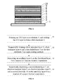
- FIG. 5 shows a spectrum comparison diagram for an organic light emitting device provided by an embodiment of the present disclosure and an organic light emitting device in the prior art.
- an embodiment of the present disclosure provides an organic light emitting device including a first electrode, a second electrode, and an organic functional layer.
- the organic functional layer may include a first doped layer fabricated in a first process, a second doped layer fabricated in a second process, and an auxiliary layer formed between the first doped layer and the second doped layer.
- the material of the auxiliary layer may be the same as the body material of the second doped layer, and the auxiliary layer is used to improve the performance of the first doped layer.
- the electron mobility of the auxiliary layer is more than 1 ⁇ 10 ⁇ 4 m 2 /V*s, and the thickness of the auxiliary layer is ranging from 1 nm to 5 nm.
- the auxiliary layer may be fabricated in the second process, i.e., the auxiliary layer and the second doped layer may be fabricated in the same process.
- the first doped layer is an organic light emitting layer.
- the second doped layer is a blue light common layer.
- the auxiliary layer is provided between the first doped layer and the second doped layer, and the material of the auxiliary layer is the same as the body material of the blue light common layer (i.e., the second doped layer), which is helpful to improve the performance of the organic light emitting layer, thereby improving the performance of the light emitting device.
- the first process for fabricating the first doped layer may be selected from one or any combination of a spin-coating method, a knife coating method, an electrospray coating method, a slit coating method, a strip coating method, a dip coating method, a drum coating method, an ink-jet printing method, a nozzle printing method, and a letterpress printing method.
- the second process for fabricating the second doped layer and the auxiliary layer may be selected from one or any combination of a vacuum thermal evaporation, an organic vapor deposition, a laser-induced thermal imaging, and a radiation-induced sublimation transfer printing.
- the organic functional layer may further include a hole injection layer, a hole transport layer, an electron transport layer, and an electron injection layer.
- Another embodiment of the present disclosure provides a method for fabricating the aforementioned organic light emitting device including sequentially forming a first electrode, an organic functional layer and a second electrode on a substrate, wherein forming the organic functional layer may include fabricating a first doped layer in a first process, forming an auxiliary layer on the first doped layer, and fabricating a second doped layer on the auxiliary layer in a second process.
- the material of the auxiliary layer may be the same as the body material of the second doped layer, and the auxiliary layer may be used to improve the performance of the first doped layer.
- the electron mobility of the auxiliary layer is more than 1 ⁇ 10 ⁇ 4 m 2 /V*s, and the thickness of the auxiliary layer is ranging from 1 nm to 5 nm.
- the auxiliary layer may be fabricated in the second process, i.e., the auxiliary layer and the second doped layer may be fabricated in the same process.
- the first doped layer may be an organic light emitting layer
- the second doped layer may be a blue light common layer.
- the first process may be selected from one or any combination of a spin-coating method, a knife coating method, an electrospray coating method, a slit coating method, a strip coating method, a dip coating method, a drum coating method, an ink-jet printing method, a nozzle printing method, and a letterpress printing method.
- the second process may be selected from one or any combination of a vacuum thermal evaporation, an organic vapor deposition, a laser-induced thermal imaging, and a radiation-induced sublimation transfer printing.
- forming the organic functional layer may further include the steps of: forming a hole injection layer on the first electrode, forming a hole transport layer on the hole injection layer, forming an electron transport layer on the second doped layer, and forming an electron injection layer on the electron transport layer.
- the display apparatus for example may be an apparatus having a display function, such as a display panel, a monitor, a tablet computer, a mobile phone, a navigator, a photo camera, a video camera, or a television.
- a display function such as a display panel, a monitor, a tablet computer, a mobile phone, a navigator, a photo camera, a video camera, or a television.
- a specific embodiment of the present disclosure is described as follows in conjunction with the cross-sectional diagram of a structure of an organic light emitting device as illustrated in FIG. 3 .
- a method for fabricating the organic light emitting device provided by the specific embodiment specifically may include the steps as follows.
- the substrate 1 may be a transparent substrate made of glass.
- the thickness of the first electrode 2 is about 70 nm.
- the ITO glass substrate may be cleaned in an ultrasonic environment of deionized water, acetone and anhydrous ethanol, then dried with nitrogen N2, and treated with oxygen plasmas.
- PEDOT:PSS poly (styrenesulfonate)
- PVK Polyviny
- the above processed substrate may be placed in an evaporation chamber, after the vacuum degree is below 5 ⁇ 10 ⁇ 4 Pa, 2-methyl-9,10-bis (naphthalen-2-yl) anthracene (MADN) is deposited in a manner of vacuum thermal evaporation to form the auxiliary layer 6 , wherein the thickness of the auxiliary layer 6 is about 2 nm.
- MADN 2-methyl-9,10-bis (naphthalen-2-yl) anthracene
- the second doped layer 7 may be deposited on the auxiliary layer 6 in a manner of vacuum thermal evaporation, wherein the second doped layer 7 is a blue light common layer, the dopant main body of which is MAND, and the dopant object is a blue fluorescent material 1-4-di-[4-(N,N-diphenyl)amino]styryl-benzene (DSA-Ph).
- DSA-Ph blue fluorescent material 1-4-di-[4-(N,N-diphenyl)amino]styryl-benzene
- the concentration of the dopant object is about 5%, and the thickness of the second doped layer 7 is about 18 nm, next, 4,7-Diphenyl-1,10-phenanthroline (Bphen) is deposited on the second doped layer 7 to form the electron transport layer 8 , wherein the thickness of the electron transport layer 8 is about 20 nm, lithium fluoride (LiF) is deposited on the electron transport layer 8 to form the electron injection layer 9 , wherein the thickness of the electron injection layer 9 is about 1 nm, aluminum (Al) is deposited on the electron injection layer to form the second electrode 10 , wherein the thickness of the second electrode 10 is about 120 nm.
- Bphen 4,7-Diphenyl-1,10-phenanthroline
- the light-emitting area of the device is 2 mm ⁇ 2 mm.
- the organic light emitting device includes a transparent ITO anode glass substrate, a hole injection layer, a hole transport layer, a first doped layer/an organic light emitting layer, a second doped layer/a blue light common layer, an electron transport layer, an electron injection layer, and a second electrode/a cathode, which are orderly laminated.
- the ITO glass substrate may be transparent glass having an ITO film
- the first electrode may be an ITO with a layer thickness of about 70 nm
- the hole injection layer may be Poly (3,4-ethylenedioxythiophene): poly (styrenesulfonate) (PEDOT: PSS);
- the hole transport layer may be Polyvinylcarbazole (PVK)
- the dopant main body of the first doped layer/green light emitting layer may be polyfluorene
- the dopant object thereof may be Tris (2-phenylpyridine) iridium (III) (Ir(ppy) 3 )
- the dopant main body of the second doped layer/blue light common layer may be 2-methyl-9,10-bis (naphthalen-2-yl) anthracene (MAND), and the dopant object thereof may be 1-4-di-[4-(N,N-diphenyl)amino] styryl-benz
- the device as illustrated in FIG. 1 may be fabricated in the following steps: the transparent glass substrate having an ITO (surface resistance thereof ⁇ 30 ⁇ / ⁇ ) is photo-etched to form an ITO pattern electrode, next the ITO glass substrate is sequentially cleaned in an ultrasonic environment of deionized water, acetone and anhydrous ethanol, then dried with nitrogen N2, and treated with oxygen plasmas; an hole injection layer PEDOT: PSS (20 nm), a hole transport layer PVK (20 nm) and a first doped layer polyfluorene: Ir (ppy) 3 (60 nm) are sequentially spin-coated on the ITO, finally, the processed substrate is placed in an evaporation chamber, after the vacuum degree is below 5 ⁇ 10 ⁇ 4 Pa, a second doped layer/blue light common layer MAND: DSA-Ph (5%) (20 nm), an electron transport layer Bphen (20 nm), an electron injection layer LiF (1 nm), and a second electrode/cathode Al (120 nm)
- the organic light emitting device under the condition that the brightness is 1000 nits, the organic light emitting device according to the embodiment of the present disclosure has an operating voltage of 5.63 V, a current efficiency of 37.1 cd/A, a power efficiency of 20.7 lm/w, a chromaticity coordinate (CIE1931) of (0.278, 0.641), and an external quantum efficiency of 10.05%, while the organic light emitting device as illustrated in FIG. 1 has an operating voltage of 5.81 V, a current efficiency of 35.5 cd/A, a power efficiency of 19.2 m/w, a chromaticity coordinate (CIE1931) of (0.278, 0.641), and an external quantum efficiency of 9.66%.
- the operating voltage of the organic light emitting device according to the embodiment of the present disclosure is lower than that of the organic light emitting device illustrated in FIG. 1 , while the current efficiency, the power efficiency and the external quantum efficiency of the organic light emitting device according to the embodiment of the present disclosure are higher than those of the organic light emitting device illustrated in FIG. 1 . Therefore, the technical solution provided by the embodiment of the present disclosure can effectively reduce the operating voltage and improve the efficiency.
- FIG. 5 shows a spectrogram comparison result for an organic light emitting device provided by an embodiment of the present disclosure and an organic light emitting device in the prior art.
- the spectrogram of the organic light emitting device provided by the embodiment of the present disclosure substantially coincides with that of the organic light emitting device in the prior art.
- the technical solution provided by the embodiment of the present disclosure does not change the light color.
- the embodiments of the present disclosure provide an organic light emitting device and a method for fabricating the same.
- an auxiliary layer made of a material the same as the body material of the second doped layer between the first doped layer and the second doped layer By adding an auxiliary layer made of a material the same as the body material of the second doped layer between the first doped layer and the second doped layer, the performance of the first doped layer can be improved, and the problem of the defective heterogeneous interface can be solved, thereby extending the lifespan of the OLED, reducing the operating voltage and improving the efficiency.
Landscapes
- Engineering & Computer Science (AREA)
- Manufacturing & Machinery (AREA)
- Physics & Mathematics (AREA)
- Optics & Photonics (AREA)
- Electroluminescent Light Sources (AREA)
Abstract
The embodiments of the present disclosure provide an organic light emitting device including a first electrode, a second electrode, and an organic functional layer, wherein the organic functional layer includes a first doped layer fabricated in a first process, a second doped layer fabricated in a second process, and an auxiliary layer formed between the first doped layer and the second doped layer, wherein the auxiliary layer is used to improve the performance of the first doped layer. The embodiments of the present disclosure further provide a method for fabricating the organic light emitting device. The embodiments of the present disclosure also provide a display apparatus including the organic light emitting device.
Description
This application is a National Stage Entry of PCT/CN2016/074134 filed Feb. 19, 2016, which claims the benefit and priority of Chinese Patent Application No. 201510130819.4, filed on Mar. 24, 2015, the disclosures of which are incorporated by reference herein in their entirety as part of the present application.
The embodiments of the present disclosure relate to the field of semiconductor fabricating technologies, and particularly, to an organic light emitting device and a method for fabricating the same, and a display apparatus.
The current solution process can fabricate green and red light devices with excellent performances, but there is still a large gap between such fabricated blue light device and the VTE-fabricated blue light device in efficiency or in lifetime. Thus, when the solution process is used to fabricate the full color Organic Light-Emitting Diode (OLED) display, an Open Mask is usually adopted to fabricate the blue light common layer. This functional layer serves as an electron transfer layer in the red and green subpixels without emitting light, while acts as a blue light emitting layer in the blue subpixels.
Usually both sides of an interface between the blue light emitting layer and the solution process light emitting layer are doped layers, and the process modes of the first and second doped layers are different from each other, which will easily cause the problems such as efficiency decrease. In the current OLED having a blue light common layer, such an interface is not efficiently improved, and thus the performance of the OLED is certainly affected.
The embodiments of the present disclosure provide an organic light emitting device and a method for fabricating the same, and a display apparatus, which are capable of improving the problem of a defective heterogeneous interface, thereby extending the lifespan of the OLED, reducing the operating voltage and improving the efficiency.
A first aspect of the embodiments of the present disclosure provides an organic light emitting device including a first electrode, a second electrode, and an organic functional layer, wherein the organic functional layer includes a first doped layer fabricated in a first process, a second doped layer fabricated in a second process, and an auxiliary layer formed between the first doped layer and the second doped layer.
In one example, the material of the auxiliary layer is the same as the body material of the second doped layer, and the auxiliary layer is used to improve the performance of the first doped layer.
In one example, the auxiliary layer has an electron mobility more than 1×10⁻⁴ m2/V*s (square meters per volt seconds).
In one example, the auxiliary layer has a thickness ranging from 1 nm to 5 nm.
In one example, the auxiliary layer is fabricated in the second process.
In one example, the first doped layer includes an organic light emitting layer, and the second doped layer includes a blue light common layer.
In one example, the first process is selected from one or any combination of a spin-coating method, a knife coating method, an electrospray coating method, a slit coating method, a strip coating method, a dip coating method, a drum coating method, an ink-jet printing method, a nozzle printing method, and a letterpress printing method.
In one example, the second process is selected from one or any combination of a vacuum thermal evaporation, an organic vapor deposition, a laser-induced thermal imaging, and a radiation-induced sublimation transfer printing.
In one example, the organic functional layer further includes a hole injection layer, a hole transport layer, an electron transport layer, and an electron injection layer.
A second aspect of the embodiments of the present disclosure provides a method for fabricating an organic light emitting device including sequentially forming a first electrode, an organic functional layer and a second electrode on a substrate, wherein, forming the organic functional layer includes fabricating a first doped layer in a first process, forming an auxiliary layer on the first doped layer, and fabricating a second doped layer on the auxiliary layer in a second process.
In one example, the material of the auxiliary layer is the same as the body material of the second doped layer, and the auxiliary layer is used to improve the performance of the first doped layer.
In one example, the auxiliary layer has an electron mobility more than 1×10⁻⁴ m2/V*s.
In one example, the auxiliary layer has a thickness ranging from 1 nm to 5 nm.
In one example, forming the auxiliary layer includes fabricating the auxiliary layer in the second process.
In one example, the first doped layer includes an organic light emitting layer, and the second doped layer includes a blue light common layer.
In one example, the first process is selected from one or any combination of a spin-coating method, a knife coating method, an electrospray coating method, a slit coating method, a strip coating method, a dip coating method, a drum coating method, an ink-jet printing method, a nozzle printing method, and a letterpress printing method.
In one example, the second process is selected from one or any combination of a vacuum thermal evaporation, an organic vapor deposition, a laser-induced thermal imaging, and a radiation-induced sublimation transfer printing.
In one example, forming the organic functional layer further includes forming a hole injection layer on the first electrode, forming a hole transport layer on the hole injection layer, forming an electron transport layer on the second doped layer, and forming an electron injection layer on the electron transport layer.
A third aspect of the embodiments of the present disclosure provides a display apparatus including any one of the aforementioned organic light emitting devices.
As can be seen from the above technical solutions, the embodiments of the present disclosure provide an organic light emitting device and a method for fabricating the same, and a display apparatus. By forming an auxiliary layer between the first doped layer and the second doped layer, the performance of the first doped layer can be improved, and the problem of the defective heterogeneous interface can be solved, thereby extending the lifespan of the OLED, reducing the operating voltage and improving the efficiency.
In order to more clearly describe the technical solutions in the embodiments of the present disclosure, the drawings to be used in the descriptions of the embodiments will be briefly introduced as follows. Obviously, the following drawings just illustrate some embodiments of the present disclosure, and a person skilled in the art can obtain other drawings from them without paying any creative effort.
The technical solutions in the embodiments of the present disclosure will now be clearly and completely described as follows in conjunction with the accompanying drawings of the embodiments of the present disclosure. It will be apparent that those described embodiments are just a part of the embodiments of the present disclosure and are not intended to be exhaustive. Based on the embodiments of the present disclosure, any other embodiment obtained by a person skilled in the art without paying any creative effort shall fall within the protection scope of the present disclosure.
As illustrated in FIG. 2 , an embodiment of the present disclosure provides an organic light emitting device including a first electrode, a second electrode, and an organic functional layer. The organic functional layer may include a first doped layer fabricated in a first process, a second doped layer fabricated in a second process, and an auxiliary layer formed between the first doped layer and the second doped layer.
In one embodiment, the material of the auxiliary layer may be the same as the body material of the second doped layer, and the auxiliary layer is used to improve the performance of the first doped layer.
In one embodiment, the electron mobility of the auxiliary layer is more than 1×10⁻⁴ m2/V*s, and the thickness of the auxiliary layer is ranging from 1 nm to 5 nm.
In one embodiment, the auxiliary layer may be fabricated in the second process, i.e., the auxiliary layer and the second doped layer may be fabricated in the same process.
In one embodiment, the first doped layer is an organic light emitting layer. The second doped layer is a blue light common layer. In the organic light emitting device provided according to the embodiment of the present disclosure, the auxiliary layer is provided between the first doped layer and the second doped layer, and the material of the auxiliary layer is the same as the body material of the blue light common layer (i.e., the second doped layer), which is helpful to improve the performance of the organic light emitting layer, thereby improving the performance of the light emitting device.
In one embodiment, the first process for fabricating the first doped layer may be selected from one or any combination of a spin-coating method, a knife coating method, an electrospray coating method, a slit coating method, a strip coating method, a dip coating method, a drum coating method, an ink-jet printing method, a nozzle printing method, and a letterpress printing method.
In one embodiment, the second process for fabricating the second doped layer and the auxiliary layer may be selected from one or any combination of a vacuum thermal evaporation, an organic vapor deposition, a laser-induced thermal imaging, and a radiation-induced sublimation transfer printing.
As illustrated in FIG. 2 , in an embodiment of the present disclosure, the organic functional layer may further include a hole injection layer, a hole transport layer, an electron transport layer, and an electron injection layer.
Another embodiment of the present disclosure provides a method for fabricating the aforementioned organic light emitting device including sequentially forming a first electrode, an organic functional layer and a second electrode on a substrate, wherein forming the organic functional layer may include fabricating a first doped layer in a first process, forming an auxiliary layer on the first doped layer, and fabricating a second doped layer on the auxiliary layer in a second process.
In one embodiment, the material of the auxiliary layer may be the same as the body material of the second doped layer, and the auxiliary layer may be used to improve the performance of the first doped layer.
In one embodiment, the electron mobility of the auxiliary layer is more than 1×10⁻⁴ m2/V*s, and the thickness of the auxiliary layer is ranging from 1 nm to 5 nm.
In one embodiment, the auxiliary layer may be fabricated in the second process, i.e., the auxiliary layer and the second doped layer may be fabricated in the same process.
In one embodiment, the first doped layer may be an organic light emitting layer, and the second doped layer may be a blue light common layer.
In one embodiment, the first process may be selected from one or any combination of a spin-coating method, a knife coating method, an electrospray coating method, a slit coating method, a strip coating method, a dip coating method, a drum coating method, an ink-jet printing method, a nozzle printing method, and a letterpress printing method.
In one embodiment, the second process may be selected from one or any combination of a vacuum thermal evaporation, an organic vapor deposition, a laser-induced thermal imaging, and a radiation-induced sublimation transfer printing.
Specifically, forming the organic functional layer may further include the steps of: forming a hole injection layer on the first electrode, forming a hole transport layer on the hole injection layer, forming an electron transport layer on the second doped layer, and forming an electron injection layer on the electron transport layer.
Another embodiment of the present disclosure provides a display apparatus including an organic light emitting device in the aforementioned embodiments. The display apparatus for example may be an apparatus having a display function, such as a display panel, a monitor, a tablet computer, a mobile phone, a navigator, a photo camera, a video camera, or a television.
In order to more clearly describe the technical solution of the present disclosure, a specific embodiment of the present disclosure is described as follows in conjunction with the cross-sectional diagram of a structure of an organic light emitting device as illustrated in FIG. 3 . As illustrated in FIG. 4 , a method for fabricating the organic light emitting device provided by the specific embodiment specifically may include the steps as follows.
S1: forming an Indium Tin Oxide (ITO) layer on a substrate 1, and etching the ITO layer to form a first electrode 2.
In this embodiment, the substrate 1 may be a transparent substrate made of glass. The thickness of the first electrode 2 is about 70 nm. To be noted, after the formation of the first electrode 2, the ITO glass substrate may be cleaned in an ultrasonic environment of deionized water, acetone and anhydrous ethanol, then dried with nitrogen N2, and treated with oxygen plasmas.
S2: sequentially forming a hole injection layer 3, a hole transport layer 4 and a first doped layer 5 on the first electrode 2 in a spin-coating method.
Specifically, Poly (3,4-ethylenedioxythiophene): poly (styrenesulfonate) (PEDOT:PSS) is spin-coated on the first electrode 2 at first to form the hole injection layer 3, wherein the thickness of the hole injection layer 3 is about 20 nm, next, Polyvinylcarbazole (PVK) is spin-coated on the hole injection layer 3 to form the hole transport layer 4, wherein the thickness of the hole transport layer 4 is about 20 nm, further, a spin-coating is performed on the hole transport layer to form the first doped layer 5, wherein the dopant main body of the first doped layer 5 may be polyfluorene, the dopant object of the first doped layer 5 may be Tris (2-phenylpyridine) iridium (III) (Ir(ppy)3), and the thickness of the first doped layer 5 is about 60 nm.
S3: depositing an auxiliary layer 6 on the first doped layer 5 in a manner of vacuum thermal evaporation.
Specifically, the above processed substrate may be placed in an evaporation chamber, after the vacuum degree is below 5×10⁻⁴ Pa, 2-methyl-9,10-bis (naphthalen-2-yl) anthracene (MADN) is deposited in a manner of vacuum thermal evaporation to form the auxiliary layer 6, wherein the thickness of the auxiliary layer 6 is about 2 nm.
S4: Sequentially depositing a second doped layer 7, an electron transport layer 8, an electron injection layer 9, and a second electrode 10 on the auxiliary layer 6 in a manner of vacuum thermal evaporation.
Specifically, the second doped layer 7 may be deposited on the auxiliary layer 6 in a manner of vacuum thermal evaporation, wherein the second doped layer 7 is a blue light common layer, the dopant main body of which is MAND, and the dopant object is a blue fluorescent material 1-4-di-[4-(N,N-diphenyl)amino]styryl-benzene (DSA-Ph). The concentration of the dopant object is about 5%, and the thickness of the second doped layer 7 is about 18 nm, next, 4,7-Diphenyl-1,10-phenanthroline (Bphen) is deposited on the second doped layer 7 to form the electron transport layer 8, wherein the thickness of the electron transport layer 8 is about 20 nm, lithium fluoride (LiF) is deposited on the electron transport layer 8 to form the electron injection layer 9, wherein the thickness of the electron injection layer 9 is about 1 nm, aluminum (Al) is deposited on the electron injection layer to form the second electrode 10, wherein the thickness of the second electrode 10 is about 120 nm.
In the above vacuum thermal evaporation process, except that Al was etched using a metal mask and the evaporation rate was 0.3 nm/s, the remaining layers were etched using an open mask and the evaporation rate was 0.1 nm/s. In this embodiment, the light-emitting area of the device is 2 mm×2 mm.
In order to reflect the technical effects of the embodiments of the present disclosure, an existing organic light emitting device will be described below.
Referring to FIG. 1 , the organic light emitting device includes a transparent ITO anode glass substrate, a hole injection layer, a hole transport layer, a first doped layer/an organic light emitting layer, a second doped layer/a blue light common layer, an electron transport layer, an electron injection layer, and a second electrode/a cathode, which are orderly laminated.
In the organic light emitting device as illustrated in FIG. 1 , the ITO glass substrate may be transparent glass having an ITO film, the first electrode may be an ITO with a layer thickness of about 70 nm, the hole injection layer may be Poly (3,4-ethylenedioxythiophene): poly (styrenesulfonate) (PEDOT: PSS); the hole transport layer may be Polyvinylcarbazole (PVK), the dopant main body of the first doped layer/green light emitting layer may be polyfluorene, and the dopant object thereof may be Tris (2-phenylpyridine) iridium (III) (Ir(ppy)3), the dopant main body of the second doped layer/blue light common layer may be 2-methyl-9,10-bis (naphthalen-2-yl) anthracene (MAND), and the dopant object thereof may be 1-4-di-[4-(N,N-diphenyl)amino] styryl-benzene (DSA-Ph), the electron transport layer may be 4,7-Diphenyl-1,10-phenanthroline (Bphen); the electron injection layer may be LiF, and the second electrode/cathode may be Al.
Similarly, the device as illustrated in FIG. 1 may be fabricated in the following steps: the transparent glass substrate having an ITO (surface resistance thereof <30Ω/□) is photo-etched to form an ITO pattern electrode, next the ITO glass substrate is sequentially cleaned in an ultrasonic environment of deionized water, acetone and anhydrous ethanol, then dried with nitrogen N2, and treated with oxygen plasmas; an hole injection layer PEDOT: PSS (20 nm), a hole transport layer PVK (20 nm) and a first doped layer polyfluorene: Ir (ppy)3 (60 nm) are sequentially spin-coated on the ITO, finally, the processed substrate is placed in an evaporation chamber, after the vacuum degree is below 5×10⁻⁴ Pa, a second doped layer/blue light common layer MAND: DSA-Ph (5%) (20 nm), an electron transport layer Bphen (20 nm), an electron injection layer LiF (1 nm), and a second electrode/cathode Al (120 nm) are sequentially deposited in a manner of vacuum thermal evaporation. In the above vacuum thermal evaporation process, except that Al was etched using a metal mask and the evaporation rate was 0.3 nm/s, the remaining layers were etched using an open mask and the evaporation rate was 0.1 nm/s, and the light-emitting area of the device was 2 mm×2 mm.
By testing the organic light emitting device provided by the above specific embodiments of the present disclosure and the existing organic light emitting device as illustrated in FIG. 1 , a comparison result can be obtained, as shown in Table 1:
| TABLE 1 |
| the comparison of Technical effects |
| 1000 nits |
| C.E. | P.E. | E.Q.E | |||||
| V | (cd/A) | (lm/w) | CIEx | CIEy | (%) | ||
| |
5.63 | 37.1 | 20.7 | 0.278 | 0.641 | 10.05 |
| Comparative | 5.81 | 35.5 | 19.2 | 0.278 | 0.641 | 9.66 |
| embodiment | ||||||
As can be seen from Table 1, under the condition that the brightness is 1000 nits, the organic light emitting device according to the embodiment of the present disclosure has an operating voltage of 5.63 V, a current efficiency of 37.1 cd/A, a power efficiency of 20.7 lm/w, a chromaticity coordinate (CIE1931) of (0.278, 0.641), and an external quantum efficiency of 10.05%, while the organic light emitting device as illustrated in FIG. 1 has an operating voltage of 5.81 V, a current efficiency of 35.5 cd/A, a power efficiency of 19.2 m/w, a chromaticity coordinate (CIE1931) of (0.278, 0.641), and an external quantum efficiency of 9.66%. It is clear that under the same brightness condition, the operating voltage of the organic light emitting device according to the embodiment of the present disclosure is lower than that of the organic light emitting device illustrated in FIG. 1 , while the current efficiency, the power efficiency and the external quantum efficiency of the organic light emitting device according to the embodiment of the present disclosure are higher than those of the organic light emitting device illustrated in FIG. 1 . Therefore, the technical solution provided by the embodiment of the present disclosure can effectively reduce the operating voltage and improve the efficiency.
The embodiments of the present disclosure provide an organic light emitting device and a method for fabricating the same. By adding an auxiliary layer made of a material the same as the body material of the second doped layer between the first doped layer and the second doped layer, the performance of the first doped layer can be improved, and the problem of the defective heterogeneous interface can be solved, thereby extending the lifespan of the OLED, reducing the operating voltage and improving the efficiency.
To be noted, in the drawings the sizes of the layers and areas might be exaggerated in order for clarity of illustration. In addition, it will be appreciated that when an element or layer is referred to as being “on” another element or layer, it may be directly located on other element, or there may be an intermediate layer; when an element or layer is referred to as being “under” another element or layer, it may be directly located under other element, or there may be more than one intermediate layer or element; and when an element or layer is referred to as being “between” two layers or elements, it may be an unique layer between the two layers or elements, or there may be more than one intermediate layer or element. Similar reference signs indicate similar elements throughout the Specification.
In the embodiments of the present disclosure, the terms “first”, “second”, and “third” are only used for the purpose of description, and cannot be construed as indicating or implying relative importance.
The above embodiments are merely illustrative of the technical solutions of the present disclosure and not intended to be limiting thereof. Although the present disclosure has been described in details with reference to the aforementioned embodiments, a person skilled in the art shall appreciate that the technical solutions described in the aforementioned embodiments still can be amended, or some technical features therein may be equivalently replaced, and such modifications or substitutions do not cause the essence of corresponding technical solution to deviate from the spirit and range of the technical solution of any embodiment of the present disclosure.
Claims (17)
1. A organic light emitting device comprising:
a first electrode;
a second electrode; and
an organic functional layer, wherein the organic functional layer comprises a first doped layer fabricated in a first process, a second doped layer fabricated in a second process, and an auxiliary layer formed between the first doped layer and the second doped layer, wherein a material of the auxiliary layer is the same as a body material of the second doped layer, and wherein the auxiliary layer is used to improve the performance of the first doped layer.
2. The organic light emitting device according to claim 1 , wherein the auxiliary layer has an electron mobility more than 1×10⁻⁴ m2/V*s (square meters per volt seconds).
3. The organic light emitting device according to claim 1 , wherein the auxiliary layer has a thickness ranging from 1 nm to 5 nm.
4. The organic light emitting device according to claim 1 , wherein the auxiliary layer is fabricated in the second process.
5. The organic light emitting device according to claim 1 , wherein the first doped layer comprises an organic light emitting layer, and wherein the second doped layer comprises a blue light common layer.
6. The organic light emitting device according to claim 1 , wherein the first process is at least one of a spin-coating method, a knife coating method, an electrospray coating method, a slit coating method, a strip coating method, a dip coating method, a drum coating method, an ink-jet printing method, a nozzle printing method, and a letterpress printing method.
7. The organic light emitting device according to claim 1 , wherein the second process is at least one of a vacuum thermal evaporation, an organic vapor deposition, a laser-induced thermal imaging, and a radiation-induced sublimation transfer printing.
8. The organic light emitting device according to claim 1 , wherein the organic functional layer further comprises a hole injection layer, a hole transport layer, an electron transport layer, and an electron injection layer.
9. A method for fabricating an organic light emitting device comprising sequentially forming a first electrode, an organic functional layer, and a second electrode on a substrate, wherein forming the organic functional layer comprises:
fabricating a first doped layer in a first process;
forming an auxiliary layer on the first doped layer; and
fabricating a second doped layer on the auxiliary layer in a second process, wherein a material of the auxiliary layer is the same as a body material of the second doped layer, and wherein the auxiliary layer is used to improve the performance of the first doped layer.
10. The method according to claim 9 , wherein forming the auxiliary layer comprises fabricating the auxiliary layer in the second process.
11. The method according to claim 9 , wherein the first doped layer includes an organic light emitting layer, and wherein the second doped layer includes a blue light common layer.
12. The method according to claim 9 , wherein the first process is at least one of a spin-coating method, a knife coating method, an electrospray coating method, a slit coating method, a strip coating method, a dip coating method, a drum coating method, an ink-jet printing method, a nozzle printing method, and a letterpress printing method.
13. The method according to claim 9 , wherein the second process is at least one of a vacuum thermal evaporation, an organic vapor deposition, a laser-induced thermal imaging, and a radiation-induced sublimation transfer printing.
14. The method according to claim 9 , wherein forming the organic functional layer further comprises:
forming a hole injection layer on the first electrode;
forming a hole transport layer on the hole injection layer;
forming an electron transport layer on the second doped layer; and
forming an electron injection layer on the electron transport layer.
15. A display apparatus comprising an organic light emitting device which comprises:
a first electrode;
a second electrode; and
an organic functional layer, wherein the organic functional layer comprises a first doped layer fabricated in a first process, a second doped layer fabricated in a second process, and an auxiliary layer formed between the first doped layer and the second doped layer, wherein a material of the auxiliary layer is the same as a body material of the second doped layer, and wherein the auxiliary layer is used to improve the performance of the first doped layer.
16. The display apparatus according to claim 15 , wherein the auxiliary layer has an electron mobility more than 1×10⁻⁴ m2/V*s (square meters per volt seconds).
17. The display apparatus according to claim 15 , wherein the auxiliary layer has a thickness ranging from 1 nm to 5 nm.
Applications Claiming Priority (4)
| Application Number | Priority Date | Filing Date | Title |
|---|---|---|---|
| CN201510130819.4 | 2015-03-24 | ||
| CN201510130819.4A CN104701458B (en) | 2015-03-24 | 2015-03-24 | A kind of organic luminescent device and preparation method thereof, display device |
| CN201510130819 | 2015-03-24 | ||
| PCT/CN2016/074134 WO2016150264A1 (en) | 2015-03-24 | 2016-02-19 | Organic light emitting device and manufacturing method therefor, and display apparatus |
Publications (3)
| Publication Number | Publication Date |
|---|---|
| US20170279062A1 US20170279062A1 (en) | 2017-09-28 |
| US20180138438A9 US20180138438A9 (en) | 2018-05-17 |
| US10026914B2 true US10026914B2 (en) | 2018-07-17 |
Family
ID=53348372
Family Applications (1)
| Application Number | Title | Priority Date | Filing Date |
|---|---|---|---|
| US15/512,099 Active US10026914B2 (en) | 2015-03-24 | 2016-02-19 | Organic light emitting device and method for fabricating the same, and display apparatus |
Country Status (3)
| Country | Link |
|---|---|
| US (1) | US10026914B2 (en) |
| CN (1) | CN104701458B (en) |
| WO (1) | WO2016150264A1 (en) |
Families Citing this family (4)
| Publication number | Priority date | Publication date | Assignee | Title |
|---|---|---|---|---|
| CN104701458B (en) * | 2015-03-24 | 2019-01-04 | 京东方科技集团股份有限公司 | A kind of organic luminescent device and preparation method thereof, display device |
| CN105185916A (en) * | 2015-07-14 | 2015-12-23 | 京东方科技集团股份有限公司 | Organic electroluminescent device, manufacturing method thereof and display device |
| CN108492759B (en) * | 2018-04-12 | 2021-04-06 | 京东方科技集团股份有限公司 | Photosensitive device, optical detection circuit, driving method and display device |
| CN110690353B (en) * | 2019-09-06 | 2021-01-15 | 深圳市华星光电半导体显示技术有限公司 | Preparation method of series OLED device |
Citations (16)
| Publication number | Priority date | Publication date | Assignee | Title |
|---|---|---|---|---|
| CN1815774A (en) | 2004-12-13 | 2006-08-09 | 株式会社丰田自动织机 | Organic el devices |
| CN1845357A (en) | 2006-03-28 | 2006-10-11 | 友达光电股份有限公司 | Organic electroluminescence device |
| CN1897295A (en) | 1996-11-25 | 2007-01-17 | 精工爱普生株式会社 | Method of manufacturing organic el element, organic el element, and organic el display device |
| CN101510589A (en) | 2002-12-26 | 2009-08-19 | 株式会社半导体能源研究所 | Organic light emitting element |
| CN102027614A (en) | 2008-05-16 | 2011-04-20 | 株式会社半导体能源研究所 | Light-emitting element, light-emitting device, and electronic device |
| US7948163B2 (en) | 2003-11-14 | 2011-05-24 | General Electric Company | Small molecule/polymer organic light emitting device capable of white light emission |
| CN102130306A (en) | 2009-11-03 | 2011-07-20 | 精工爱普生株式会社 | Organic EL device manufacturing method, organic EL device, and electronic apparatus |
| CN102800812A (en) | 2011-05-23 | 2012-11-28 | 三星移动显示器株式会社 | Organic light-emitting device |
| CN103579522A (en) | 2012-07-24 | 2014-02-12 | 三星显示有限公司 | Organic light-emitting device and organic light-emitting display apparatus including the same |
| CN103682116A (en) | 2013-12-02 | 2014-03-26 | 京东方科技集团股份有限公司 | OLED (organic light emitting diode) device and display device |
| CN104022229A (en) | 2014-05-30 | 2014-09-03 | 京东方科技集团股份有限公司 | OLED device, manufacturing method thereof and display device |
| CN104078485A (en) | 2013-03-26 | 2014-10-01 | 三星显示有限公司 | Organic light-emitting display device, method of manufacturing the same, and donor substrate and donor substrate set used to manufacture the organic light-emitting display device |
| CN104218049A (en) | 2013-05-29 | 2014-12-17 | 三星显示有限公司 | Organic light-emitting display device and method of manufacturing the same |
| US20150069366A1 (en) * | 2013-09-12 | 2015-03-12 | Board Of Trustees Of Michigan State University | Nanocluster Based Light Emitting Device |
| CN104701458A (en) | 2015-03-24 | 2015-06-10 | 京东方科技集团股份有限公司 | Organic light emitting device and manufacturing method thereof and display device |
| US20160218154A1 (en) * | 2015-01-23 | 2016-07-28 | Samsung Display Co., Ltd. | Organic electroluminescent display apparatus |
-
2015
- 2015-03-24 CN CN201510130819.4A patent/CN104701458B/en active Active
-
2016
- 2016-02-19 WO PCT/CN2016/074134 patent/WO2016150264A1/en active Application Filing
- 2016-02-19 US US15/512,099 patent/US10026914B2/en active Active
Patent Citations (17)
| Publication number | Priority date | Publication date | Assignee | Title |
|---|---|---|---|---|
| CN1897295A (en) | 1996-11-25 | 2007-01-17 | 精工爱普生株式会社 | Method of manufacturing organic el element, organic el element, and organic el display device |
| CN101510589A (en) | 2002-12-26 | 2009-08-19 | 株式会社半导体能源研究所 | Organic light emitting element |
| US7948163B2 (en) | 2003-11-14 | 2011-05-24 | General Electric Company | Small molecule/polymer organic light emitting device capable of white light emission |
| CN1815774A (en) | 2004-12-13 | 2006-08-09 | 株式会社丰田自动织机 | Organic el devices |
| CN1845357A (en) | 2006-03-28 | 2006-10-11 | 友达光电股份有限公司 | Organic electroluminescence device |
| CN102027614A (en) | 2008-05-16 | 2011-04-20 | 株式会社半导体能源研究所 | Light-emitting element, light-emitting device, and electronic device |
| CN102130306A (en) | 2009-11-03 | 2011-07-20 | 精工爱普生株式会社 | Organic EL device manufacturing method, organic EL device, and electronic apparatus |
| CN102800812A (en) | 2011-05-23 | 2012-11-28 | 三星移动显示器株式会社 | Organic light-emitting device |
| CN103579522A (en) | 2012-07-24 | 2014-02-12 | 三星显示有限公司 | Organic light-emitting device and organic light-emitting display apparatus including the same |
| CN104078485A (en) | 2013-03-26 | 2014-10-01 | 三星显示有限公司 | Organic light-emitting display device, method of manufacturing the same, and donor substrate and donor substrate set used to manufacture the organic light-emitting display device |
| US20140291627A1 (en) * | 2013-03-26 | 2014-10-02 | Samsung Display Co., Ltd. | Organic light-emitting display device, method of manufacturing the same, and donor substrate and donor substrate set used to manufacture the organic light-emitting display device |
| CN104218049A (en) | 2013-05-29 | 2014-12-17 | 三星显示有限公司 | Organic light-emitting display device and method of manufacturing the same |
| US20150069366A1 (en) * | 2013-09-12 | 2015-03-12 | Board Of Trustees Of Michigan State University | Nanocluster Based Light Emitting Device |
| CN103682116A (en) | 2013-12-02 | 2014-03-26 | 京东方科技集团股份有限公司 | OLED (organic light emitting diode) device and display device |
| CN104022229A (en) | 2014-05-30 | 2014-09-03 | 京东方科技集团股份有限公司 | OLED device, manufacturing method thereof and display device |
| US20160218154A1 (en) * | 2015-01-23 | 2016-07-28 | Samsung Display Co., Ltd. | Organic electroluminescent display apparatus |
| CN104701458A (en) | 2015-03-24 | 2015-06-10 | 京东方科技集团股份有限公司 | Organic light emitting device and manufacturing method thereof and display device |
Non-Patent Citations (6)
| Title |
|---|
| China First Office Action, Application No. 2015101308194, dated Jun. 2, 2016, 17 pps.: with English Translation. |
| China Rejection, Application No. 2015101308194, dated Mar. 3, 2017, 14 pps.: with English Translation. |
| China Second Office Action, Application No. 2015101308194, dated Nov. 7, 2016, 14 pps.: with English Translation. |
| English Translation of PCT International Search Report, Application No. PCT/CN2016/074134, dated May 18, 2016, 2 pps. |
| PCT Written Opinion, Application No. PCT/CN2016/074134, dated May 18, 2016, 10 pps.: with English Translation. |
| Xiaolong Yang et al., "Thiazole-based metallophosphors of iridium with balanced carrier injection/transporting features and their two-colour WOLEDs fabricated by both vacuum deposition and solution processing-vacuum deposition hybrid strategy", Journals of Materials Chemistry | 2012 | 22| pp. 7136-7148 (13 total). |
Also Published As
| Publication number | Publication date |
|---|---|
| CN104701458B (en) | 2019-01-04 |
| WO2016150264A1 (en) | 2016-09-29 |
| CN104701458A (en) | 2015-06-10 |
| US20180138438A9 (en) | 2018-05-17 |
| US20170279062A1 (en) | 2017-09-28 |
Similar Documents
| Publication | Publication Date | Title |
|---|---|---|
| US10411223B2 (en) | Organic electroluminescence device and illumination device | |
| EP3321986B1 (en) | Organic light emitting diode and organic light emitting diode display device including the same | |
| US10026914B2 (en) | Organic light emitting device and method for fabricating the same, and display apparatus | |
| US10784321B2 (en) | Method for manufacturing OLED device, OLED device and display panel | |
| US10147898B2 (en) | Organic light-emitting device and display device | |
| US20170047553A1 (en) | Organic light-emitting diode and manufacturing method thereof | |
| US11737296B2 (en) | OLED display device, display panel and manufacturing method of OLED display device | |
| US8785918B2 (en) | Organic light emitting device and organic light emitting display device using the same | |
| JP2014225329A (en) | Light-emitting device, display device, and illuminating device | |
| US9748524B2 (en) | Light-emitting member and method for preparing the same as well as display device | |
| US9825101B2 (en) | Top-emitting OLED substrate and fabrication method thereof, and display apparatus | |
| US9570519B2 (en) | Organic light emitting display device with multi-organic layers | |
| US20210336177A1 (en) | Oled display panel and oled display device | |
| US20170207407A1 (en) | Organic light emitting apparatus, display device having the same, and fabricating method thereof | |
| KR20150080153A (en) | Organic Light Emitting Diode And Organic Light Emitting Diode Display Device Including The Same | |
| US20140087312A1 (en) | Method for manufacturing of organic light emitting display device | |
| US10476022B2 (en) | Organic light emitting diode and manufacturing method thereof, display apparatus | |
| US20150137086A1 (en) | Organic electroluminescence unit, method of manufacturing the same, and electronic apparatus | |
| WO2011024346A1 (en) | Organic electroluminescent element, organic electroluminescent display device, and organic electroluminescent illuminating device | |
| US9590200B2 (en) | Organic light emitting device, method of manufacturing the same, and organic light emitting display apparatus using the same | |
| WO2015190550A1 (en) | Organic element | |
| CN111490070B (en) | Display panel | |
| KR102057920B1 (en) | Organic Light Emitting Display Device and fabricating of the same | |
| KR101650780B1 (en) | Light extraction layer for top emitting organic light emitting diode and manufacturing method of thereof | |
| JP2014225323A (en) | Light-emitting device, display device, and illuminating device |
Legal Events
| Date | Code | Title | Description |
|---|---|---|---|
| AS | Assignment |
Owner name: BOE TECHNOLOGY GROUP CO., LTD, CHINA Free format text: ASSIGNMENT OF ASSIGNORS INTEREST;ASSIGNORS:YAN, GUANG;LIAO, CHIN-LUNG;SIGNING DATES FROM 20170217 TO 20170317;REEL/FRAME:041605/0167 |
|
| STCF | Information on status: patent grant |
Free format text: PATENTED CASE |
|
| MAFP | Maintenance fee payment |
Free format text: PAYMENT OF MAINTENANCE FEE, 4TH YEAR, LARGE ENTITY (ORIGINAL EVENT CODE: M1551); ENTITY STATUS OF PATENT OWNER: LARGE ENTITY Year of fee payment: 4 |