US10020188B2 - Method for depositing ALD films using halide-based precursors - Google Patents
Method for depositing ALD films using halide-based precursors Download PDFInfo
- Publication number
- US10020188B2 US10020188B2 US15/817,579 US201715817579A US10020188B2 US 10020188 B2 US10020188 B2 US 10020188B2 US 201715817579 A US201715817579 A US 201715817579A US 10020188 B2 US10020188 B2 US 10020188B2
- Authority
- US
- United States
- Prior art keywords
- reaction chamber
- pedestal
- reactant
- ald
- showerhead
- Prior art date
- Legal status (The legal status is an assumption and is not a legal conclusion. Google has not performed a legal analysis and makes no representation as to the accuracy of the status listed.)
- Active
Links
Images


Classifications
-
- H—ELECTRICITY
- H10—SEMICONDUCTOR DEVICES; ELECTRIC SOLID-STATE DEVICES NOT OTHERWISE PROVIDED FOR
- H10P—GENERIC PROCESSES OR APPARATUS FOR THE MANUFACTURE OR TREATMENT OF DEVICES COVERED BY CLASS H10
- H10P14/00—Formation of materials, e.g. in the shape of layers or pillars
- H10P14/60—Formation of materials, e.g. in the shape of layers or pillars of insulating materials
- H10P14/63—Formation of materials, e.g. in the shape of layers or pillars of insulating materials characterised by the formation processes
- H10P14/6326—Deposition processes
- H10P14/6328—Deposition from the gas or vapour phase
- H10P14/6334—Deposition from the gas or vapour phase using decomposition or reaction of gaseous or vapour phase compounds, i.e. chemical vapour deposition
- H10P14/6339—Deposition from the gas or vapour phase using decomposition or reaction of gaseous or vapour phase compounds, i.e. chemical vapour deposition deposition by cyclic CVD, e.g. ALD, ALE or pulsed CVD
-
- H01L21/0228—
-
- C—CHEMISTRY; METALLURGY
- C23—COATING METALLIC MATERIAL; COATING MATERIAL WITH METALLIC MATERIAL; CHEMICAL SURFACE TREATMENT; DIFFUSION TREATMENT OF METALLIC MATERIAL; COATING BY VACUUM EVAPORATION, BY SPUTTERING, BY ION IMPLANTATION OR BY CHEMICAL VAPOUR DEPOSITION, IN GENERAL; INHIBITING CORROSION OF METALLIC MATERIAL OR INCRUSTATION IN GENERAL
- C23C—COATING METALLIC MATERIAL; COATING MATERIAL WITH METALLIC MATERIAL; SURFACE TREATMENT OF METALLIC MATERIAL BY DIFFUSION INTO THE SURFACE, BY CHEMICAL CONVERSION OR SUBSTITUTION; COATING BY VACUUM EVAPORATION, BY SPUTTERING, BY ION IMPLANTATION OR BY CHEMICAL VAPOUR DEPOSITION, IN GENERAL
- C23C16/00—Chemical coating by decomposition of gaseous compounds, without leaving reaction products of surface material in the coating, i.e. chemical vapour deposition [CVD] processes
- C23C16/02—Pretreatment of the material to be coated
- C23C16/0227—Pretreatment of the material to be coated by cleaning or etching
-
- C—CHEMISTRY; METALLURGY
- C23—COATING METALLIC MATERIAL; COATING MATERIAL WITH METALLIC MATERIAL; CHEMICAL SURFACE TREATMENT; DIFFUSION TREATMENT OF METALLIC MATERIAL; COATING BY VACUUM EVAPORATION, BY SPUTTERING, BY ION IMPLANTATION OR BY CHEMICAL VAPOUR DEPOSITION, IN GENERAL; INHIBITING CORROSION OF METALLIC MATERIAL OR INCRUSTATION IN GENERAL
- C23C—COATING METALLIC MATERIAL; COATING MATERIAL WITH METALLIC MATERIAL; SURFACE TREATMENT OF METALLIC MATERIAL BY DIFFUSION INTO THE SURFACE, BY CHEMICAL CONVERSION OR SUBSTITUTION; COATING BY VACUUM EVAPORATION, BY SPUTTERING, BY ION IMPLANTATION OR BY CHEMICAL VAPOUR DEPOSITION, IN GENERAL
- C23C16/00—Chemical coating by decomposition of gaseous compounds, without leaving reaction products of surface material in the coating, i.e. chemical vapour deposition [CVD] processes
- C23C16/02—Pretreatment of the material to be coated
- C23C16/0272—Deposition of sub-layers, e.g. to promote the adhesion of the main coating
-
- C—CHEMISTRY; METALLURGY
- C23—COATING METALLIC MATERIAL; COATING MATERIAL WITH METALLIC MATERIAL; CHEMICAL SURFACE TREATMENT; DIFFUSION TREATMENT OF METALLIC MATERIAL; COATING BY VACUUM EVAPORATION, BY SPUTTERING, BY ION IMPLANTATION OR BY CHEMICAL VAPOUR DEPOSITION, IN GENERAL; INHIBITING CORROSION OF METALLIC MATERIAL OR INCRUSTATION IN GENERAL
- C23C—COATING METALLIC MATERIAL; COATING MATERIAL WITH METALLIC MATERIAL; SURFACE TREATMENT OF METALLIC MATERIAL BY DIFFUSION INTO THE SURFACE, BY CHEMICAL CONVERSION OR SUBSTITUTION; COATING BY VACUUM EVAPORATION, BY SPUTTERING, BY ION IMPLANTATION OR BY CHEMICAL VAPOUR DEPOSITION, IN GENERAL
- C23C16/00—Chemical coating by decomposition of gaseous compounds, without leaving reaction products of surface material in the coating, i.e. chemical vapour deposition [CVD] processes
- C23C16/22—Chemical coating by decomposition of gaseous compounds, without leaving reaction products of surface material in the coating, i.e. chemical vapour deposition [CVD] processes characterised by the deposition of inorganic material, other than metallic material
- C23C16/30—Deposition of compounds, mixtures or solid solutions, e.g. borides, carbides, nitrides
- C23C16/34—Nitrides
- C23C16/345—Silicon nitride
-
- C—CHEMISTRY; METALLURGY
- C23—COATING METALLIC MATERIAL; COATING MATERIAL WITH METALLIC MATERIAL; CHEMICAL SURFACE TREATMENT; DIFFUSION TREATMENT OF METALLIC MATERIAL; COATING BY VACUUM EVAPORATION, BY SPUTTERING, BY ION IMPLANTATION OR BY CHEMICAL VAPOUR DEPOSITION, IN GENERAL; INHIBITING CORROSION OF METALLIC MATERIAL OR INCRUSTATION IN GENERAL
- C23C—COATING METALLIC MATERIAL; COATING MATERIAL WITH METALLIC MATERIAL; SURFACE TREATMENT OF METALLIC MATERIAL BY DIFFUSION INTO THE SURFACE, BY CHEMICAL CONVERSION OR SUBSTITUTION; COATING BY VACUUM EVAPORATION, BY SPUTTERING, BY ION IMPLANTATION OR BY CHEMICAL VAPOUR DEPOSITION, IN GENERAL
- C23C16/00—Chemical coating by decomposition of gaseous compounds, without leaving reaction products of surface material in the coating, i.e. chemical vapour deposition [CVD] processes
- C23C16/22—Chemical coating by decomposition of gaseous compounds, without leaving reaction products of surface material in the coating, i.e. chemical vapour deposition [CVD] processes characterised by the deposition of inorganic material, other than metallic material
- C23C16/30—Deposition of compounds, mixtures or solid solutions, e.g. borides, carbides, nitrides
- C23C16/40—Oxides
- C23C16/401—Oxides containing silicon
- C23C16/402—Silicon dioxide
-
- C—CHEMISTRY; METALLURGY
- C23—COATING METALLIC MATERIAL; COATING MATERIAL WITH METALLIC MATERIAL; CHEMICAL SURFACE TREATMENT; DIFFUSION TREATMENT OF METALLIC MATERIAL; COATING BY VACUUM EVAPORATION, BY SPUTTERING, BY ION IMPLANTATION OR BY CHEMICAL VAPOUR DEPOSITION, IN GENERAL; INHIBITING CORROSION OF METALLIC MATERIAL OR INCRUSTATION IN GENERAL
- C23C—COATING METALLIC MATERIAL; COATING MATERIAL WITH METALLIC MATERIAL; SURFACE TREATMENT OF METALLIC MATERIAL BY DIFFUSION INTO THE SURFACE, BY CHEMICAL CONVERSION OR SUBSTITUTION; COATING BY VACUUM EVAPORATION, BY SPUTTERING, BY ION IMPLANTATION OR BY CHEMICAL VAPOUR DEPOSITION, IN GENERAL
- C23C16/00—Chemical coating by decomposition of gaseous compounds, without leaving reaction products of surface material in the coating, i.e. chemical vapour deposition [CVD] processes
- C23C16/44—Chemical coating by decomposition of gaseous compounds, without leaving reaction products of surface material in the coating, i.e. chemical vapour deposition [CVD] processes characterised by the method of coating
- C23C16/4401—Means for minimising impurities, e.g. dust, moisture or residual gas, in the reaction chamber
- C23C16/4404—Coatings or surface treatment on the inside of the reaction chamber or on parts thereof
-
- C—CHEMISTRY; METALLURGY
- C23—COATING METALLIC MATERIAL; COATING MATERIAL WITH METALLIC MATERIAL; CHEMICAL SURFACE TREATMENT; DIFFUSION TREATMENT OF METALLIC MATERIAL; COATING BY VACUUM EVAPORATION, BY SPUTTERING, BY ION IMPLANTATION OR BY CHEMICAL VAPOUR DEPOSITION, IN GENERAL; INHIBITING CORROSION OF METALLIC MATERIAL OR INCRUSTATION IN GENERAL
- C23C—COATING METALLIC MATERIAL; COATING MATERIAL WITH METALLIC MATERIAL; SURFACE TREATMENT OF METALLIC MATERIAL BY DIFFUSION INTO THE SURFACE, BY CHEMICAL CONVERSION OR SUBSTITUTION; COATING BY VACUUM EVAPORATION, BY SPUTTERING, BY ION IMPLANTATION OR BY CHEMICAL VAPOUR DEPOSITION, IN GENERAL
- C23C16/00—Chemical coating by decomposition of gaseous compounds, without leaving reaction products of surface material in the coating, i.e. chemical vapour deposition [CVD] processes
- C23C16/44—Chemical coating by decomposition of gaseous compounds, without leaving reaction products of surface material in the coating, i.e. chemical vapour deposition [CVD] processes characterised by the method of coating
- C23C16/4401—Means for minimising impurities, e.g. dust, moisture or residual gas, in the reaction chamber
- C23C16/4405—Cleaning of reactor or parts inside the reactor by using reactive gases
-
- C—CHEMISTRY; METALLURGY
- C23—COATING METALLIC MATERIAL; COATING MATERIAL WITH METALLIC MATERIAL; CHEMICAL SURFACE TREATMENT; DIFFUSION TREATMENT OF METALLIC MATERIAL; COATING BY VACUUM EVAPORATION, BY SPUTTERING, BY ION IMPLANTATION OR BY CHEMICAL VAPOUR DEPOSITION, IN GENERAL; INHIBITING CORROSION OF METALLIC MATERIAL OR INCRUSTATION IN GENERAL
- C23C—COATING METALLIC MATERIAL; COATING MATERIAL WITH METALLIC MATERIAL; SURFACE TREATMENT OF METALLIC MATERIAL BY DIFFUSION INTO THE SURFACE, BY CHEMICAL CONVERSION OR SUBSTITUTION; COATING BY VACUUM EVAPORATION, BY SPUTTERING, BY ION IMPLANTATION OR BY CHEMICAL VAPOUR DEPOSITION, IN GENERAL
- C23C16/00—Chemical coating by decomposition of gaseous compounds, without leaving reaction products of surface material in the coating, i.e. chemical vapour deposition [CVD] processes
- C23C16/44—Chemical coating by decomposition of gaseous compounds, without leaving reaction products of surface material in the coating, i.e. chemical vapour deposition [CVD] processes characterised by the method of coating
- C23C16/455—Chemical coating by decomposition of gaseous compounds, without leaving reaction products of surface material in the coating, i.e. chemical vapour deposition [CVD] processes characterised by the method of coating characterised by the method used for introducing gases into reaction chamber or for modifying gas flows in reaction chamber
- C23C16/45523—Pulsed gas flow or change of composition over time
- C23C16/45525—Atomic layer deposition [ALD]
- C23C16/45527—Atomic layer deposition [ALD] characterized by the ALD cycle, e.g. different flows or temperatures during half-reactions, unusual pulsing sequence, use of precursor mixtures or auxiliary reactants or activations
- C23C16/45536—Use of plasma, radiation or electromagnetic fields
- C23C16/4554—Plasma being used non-continuously in between ALD reactions
-
- C—CHEMISTRY; METALLURGY
- C23—COATING METALLIC MATERIAL; COATING MATERIAL WITH METALLIC MATERIAL; CHEMICAL SURFACE TREATMENT; DIFFUSION TREATMENT OF METALLIC MATERIAL; COATING BY VACUUM EVAPORATION, BY SPUTTERING, BY ION IMPLANTATION OR BY CHEMICAL VAPOUR DEPOSITION, IN GENERAL; INHIBITING CORROSION OF METALLIC MATERIAL OR INCRUSTATION IN GENERAL
- C23C—COATING METALLIC MATERIAL; COATING MATERIAL WITH METALLIC MATERIAL; SURFACE TREATMENT OF METALLIC MATERIAL BY DIFFUSION INTO THE SURFACE, BY CHEMICAL CONVERSION OR SUBSTITUTION; COATING BY VACUUM EVAPORATION, BY SPUTTERING, BY ION IMPLANTATION OR BY CHEMICAL VAPOUR DEPOSITION, IN GENERAL
- C23C16/00—Chemical coating by decomposition of gaseous compounds, without leaving reaction products of surface material in the coating, i.e. chemical vapour deposition [CVD] processes
- C23C16/44—Chemical coating by decomposition of gaseous compounds, without leaving reaction products of surface material in the coating, i.e. chemical vapour deposition [CVD] processes characterised by the method of coating
- C23C16/50—Chemical coating by decomposition of gaseous compounds, without leaving reaction products of surface material in the coating, i.e. chemical vapour deposition [CVD] processes characterised by the method of coating using electric discharges
-
- H—ELECTRICITY
- H01—ELECTRIC ELEMENTS
- H01J—ELECTRIC DISCHARGE TUBES OR DISCHARGE LAMPS
- H01J37/00—Discharge tubes with provision for introducing objects or material to be exposed to the discharge, e.g. for the purpose of examination or processing thereof
- H01J37/32—Gas-filled discharge tubes
- H01J37/32009—Arrangements for generation of plasma specially adapted for examination or treatment of objects, e.g. plasma sources
- H01J37/32082—Radio frequency generated discharge
-
- H—ELECTRICITY
- H01—ELECTRIC ELEMENTS
- H01J—ELECTRIC DISCHARGE TUBES OR DISCHARGE LAMPS
- H01J37/00—Discharge tubes with provision for introducing objects or material to be exposed to the discharge, e.g. for the purpose of examination or processing thereof
- H01J37/32—Gas-filled discharge tubes
- H01J37/32431—Constructional details of the reactor
- H01J37/32458—Vessel
- H01J37/32467—Material
-
- H—ELECTRICITY
- H01—ELECTRIC ELEMENTS
- H01J—ELECTRIC DISCHARGE TUBES OR DISCHARGE LAMPS
- H01J37/00—Discharge tubes with provision for introducing objects or material to be exposed to the discharge, e.g. for the purpose of examination or processing thereof
- H01J37/32—Gas-filled discharge tubes
- H01J37/32431—Constructional details of the reactor
- H01J37/32458—Vessel
- H01J37/32513—Sealing means, e.g. sealing between different parts of the vessel
-
- H—ELECTRICITY
- H01—ELECTRIC ELEMENTS
- H01J—ELECTRIC DISCHARGE TUBES OR DISCHARGE LAMPS
- H01J37/00—Discharge tubes with provision for introducing objects or material to be exposed to the discharge, e.g. for the purpose of examination or processing thereof
- H01J37/32—Gas-filled discharge tubes
- H01J37/32431—Constructional details of the reactor
- H01J37/32532—Electrodes
- H01J37/3255—Material
-
- H—ELECTRICITY
- H01—ELECTRIC ELEMENTS
- H01J—ELECTRIC DISCHARGE TUBES OR DISCHARGE LAMPS
- H01J37/00—Discharge tubes with provision for introducing objects or material to be exposed to the discharge, e.g. for the purpose of examination or processing thereof
- H01J37/32—Gas-filled discharge tubes
- H01J37/32431—Constructional details of the reactor
- H01J37/32715—Workpiece holder
-
- H—ELECTRICITY
- H01—ELECTRIC ELEMENTS
- H01J—ELECTRIC DISCHARGE TUBES OR DISCHARGE LAMPS
- H01J37/00—Discharge tubes with provision for introducing objects or material to be exposed to the discharge, e.g. for the purpose of examination or processing thereof
- H01J37/32—Gas-filled discharge tubes
- H01J37/32431—Constructional details of the reactor
- H01J37/32798—Further details of plasma apparatus not provided for in groups H01J37/3244 - H01J37/32788; special provisions for cleaning or maintenance of the apparatus
- H01J37/32853—Hygiene
- H01J37/32862—In situ cleaning of vessels and/or internal parts
-
- H01L21/0217—
-
- H01L21/02211—
-
- H01L21/02274—
-
- H—ELECTRICITY
- H10—SEMICONDUCTOR DEVICES; ELECTRIC SOLID-STATE DEVICES NOT OTHERWISE PROVIDED FOR
- H10P—GENERIC PROCESSES OR APPARATUS FOR THE MANUFACTURE OR TREATMENT OF DEVICES COVERED BY CLASS H10
- H10P14/00—Formation of materials, e.g. in the shape of layers or pillars
- H10P14/60—Formation of materials, e.g. in the shape of layers or pillars of insulating materials
- H10P14/63—Formation of materials, e.g. in the shape of layers or pillars of insulating materials characterised by the formation processes
- H10P14/6326—Deposition processes
- H10P14/6328—Deposition from the gas or vapour phase
- H10P14/6334—Deposition from the gas or vapour phase using decomposition or reaction of gaseous or vapour phase compounds, i.e. chemical vapour deposition
- H10P14/6336—Deposition from the gas or vapour phase using decomposition or reaction of gaseous or vapour phase compounds, i.e. chemical vapour deposition in the presence of a plasma [PECVD]
-
- H—ELECTRICITY
- H10—SEMICONDUCTOR DEVICES; ELECTRIC SOLID-STATE DEVICES NOT OTHERWISE PROVIDED FOR
- H10P—GENERIC PROCESSES OR APPARATUS FOR THE MANUFACTURE OR TREATMENT OF DEVICES COVERED BY CLASS H10
- H10P14/00—Formation of materials, e.g. in the shape of layers or pillars
- H10P14/60—Formation of materials, e.g. in the shape of layers or pillars of insulating materials
- H10P14/66—Formation of materials, e.g. in the shape of layers or pillars of insulating materials characterised by the type of materials
- H10P14/668—Formation of materials, e.g. in the shape of layers or pillars of insulating materials characterised by the type of materials the materials being characterised by the deposition precursor materials
- H10P14/6681—Formation of materials, e.g. in the shape of layers or pillars of insulating materials characterised by the type of materials the materials being characterised by the deposition precursor materials the precursor containing a compound comprising Si
- H10P14/6682—Formation of materials, e.g. in the shape of layers or pillars of insulating materials characterised by the type of materials the materials being characterised by the deposition precursor materials the precursor containing a compound comprising Si the compound being a silane, e.g. disilane, methylsilane or chlorosilane
-
- H—ELECTRICITY
- H10—SEMICONDUCTOR DEVICES; ELECTRIC SOLID-STATE DEVICES NOT OTHERWISE PROVIDED FOR
- H10P—GENERIC PROCESSES OR APPARATUS FOR THE MANUFACTURE OR TREATMENT OF DEVICES COVERED BY CLASS H10
- H10P14/00—Formation of materials, e.g. in the shape of layers or pillars
- H10P14/60—Formation of materials, e.g. in the shape of layers or pillars of insulating materials
- H10P14/69—Inorganic materials
- H10P14/694—Inorganic materials composed of nitrides
- H10P14/6943—Inorganic materials composed of nitrides containing silicon
- H10P14/69433—Inorganic materials composed of nitrides containing silicon the material being a silicon nitride not containing oxygen, e.g. SixNy or SixByNz
-
- H—ELECTRICITY
- H01—ELECTRIC ELEMENTS
- H01J—ELECTRIC DISCHARGE TUBES OR DISCHARGE LAMPS
- H01J2237/00—Discharge tubes exposing object to beam, e.g. for analysis treatment, etching, imaging
- H01J2237/32—Processing objects by plasma generation
- H01J2237/33—Processing objects by plasma generation characterised by the type of processing
- H01J2237/332—Coating
- H01J2237/3321—CVD [Chemical Vapor Deposition]
-
- H—ELECTRICITY
- H01—ELECTRIC ELEMENTS
- H01J—ELECTRIC DISCHARGE TUBES OR DISCHARGE LAMPS
- H01J2237/00—Discharge tubes exposing object to beam, e.g. for analysis treatment, etching, imaging
- H01J2237/32—Processing objects by plasma generation
- H01J2237/33—Processing objects by plasma generation characterised by the type of processing
- H01J2237/335—Cleaning
Definitions
- a method of depositing silicon nitride films on a semiconductor substrate processed in a micro-volume of a plasma enhanced atomic layer deposition (PEALD) reaction chamber wherein the semiconductor substrate is supported on a ceramic surface of a pedestal and process gas is introduced through gas outlets in a ceramic surface of a showerhead into a reaction zone above the semiconductor substrate.
- the method includes cleaning the ceramic surfaces, depositing an undercoating on the ceramic surfaces, depositing a pre-coating over the undercoating, and sequentially processing a batch of semiconductor substrates in the processing region by transferring the semiconductor substrates one at a time into the processing region and depositing a silicon nitride film on each semiconductor substrate. After a predetermined number of semiconductor substrates are processed and/or film accumulation on the interior surfaces reaches a predetermined thickness, the cleaning, undercoating and pre-coating steps can be repeated before processing another batch of semiconductor substrates.
- PEALD plasma enhanced atomic layer deposition
- silicon nitride films are deposited on semiconductor substrates processed in a plasma enhanced atomic layer deposition (PEALD) reaction chamber wherein a single semiconductor substrate is supported on a ceramic surface of a pedestal and process gas is introduced through gas outlets in a ceramic surface of a showerhead into a reaction zone above the semiconductor substrate.
- PEALD plasma enhanced atomic layer deposition
- the method comprises (a) cleaning the ceramic surfaces of the pedestal and showerhead with a fluorine plasma, (b) depositing a halide-free atomic layer deposition (ALD) oxide undercoating on the ceramic surfaces, (c) depositing a pre-coating of ALD silicon nitride on the halide-free ALD oxide undercoating, and (d) processing a batch of semiconductor substrates by sequentially transferring each semiconductor substrate into the reaction chamber and depositing a film of ALD silicon nitride on the semiconductor substrate supported on the ceramic surface of the pedestal.
- ALD atomic layer deposition
- the method can be carried out by (i) introducing a flow of a halogen-free silicon-containing first reactant in vapor phase into the reaction chamber and allowing the first reactant to adsorb onto the ceramic surfaces of the reaction chamber; (ii) introducing a flow of an oxygen-containing second reactant in vapor phase into the reaction chamber while the first reactant is adsorbed on the ceramic surfaces of the reaction chamber; and (iii) exposing the reaction chamber to plasma when the flow of at least one of the first and second reactants has ceased, in order to drive a reaction between the first and second reactants on the ceramic surfaces of the reaction chamber to form the undercoating, where the undercoating conformally coats the ceramic surfaces of the reaction chamber; wherein operations (i)-(iii) occur when there is no semiconductor substrate present in the reaction chamber, and wherein operations (i)-(iii) are repeated until the undercoating is at least about 500 ⁇ thick.
- films are deposited on semiconductor substrates processed in a micro-volume of a plasma enhanced atomic layer deposition (PEALD) reaction chamber wherein a single semiconductor substrate is supported on a ceramic surface of a pedestal and process gas is introduced through gas outlets in a ceramic surface of a showerhead into a reaction zone above the semiconductor substrate.
- PEALD plasma enhanced atomic layer deposition
- the method comprises (a) cleaning the ceramic surfaces of the pedestal and showerhead with a fluorine plasma such that aluminum-rich byproducts are formed on the ceramic surfaces; (b) depositing a conformal halide-free atomic layer deposition (ALD) oxide undercoating on the ceramic surfaces so as to cover the aluminum-rich byproducts; (c) depositing a pre-coating on the halide-free ALD oxide undercoating; and (d) processing a batch of semiconductor substrates by transferring each semiconductor substrate into the reaction chamber and depositing a film on the semiconductor substrate supported on the ceramic surface of the pedestal.
- ALD atomic layer deposition
- the conformal halide-free ALD oxide undercoating can be formed by (i) introducing a flow of a halogen-free silicon-containing first reactant in vapor phase into the reaction chamber and allowing the first reactant to adsorb onto the interior surfaces of the reaction chamber; (ii) introducing a flow of an oxygen-containing second reactant in vapor phase into the reaction chamber while the first reactant is adsorbed on the interior surfaces of the reaction chamber; and (iii) exposing the reaction chamber to plasma when the flow of at least one of the first and second reactants has ceased, in order to drive a reaction between the first and second reactants on the interior surfaces of the reaction chamber to form the undercoating, where the undercoating conformally coats the interior surfaces of the reaction chamber; where operations (i)-(iii) occur when there is no substrate present in the reaction chamber, and where operations (i)-(iii) are repeated until the undercoating is at least about 500 ⁇ thick.
- the ceramic surfaces of the showerhead and pedestal are aluminum nitride
- step (a) is carried out at with the pedestal and showerhead at a temperature below 400° C.
- step (c) is carried out with the pedestal and showerhead at a temperature above 400° C.
- the undercoating can be deposited to a thickness of at least 500 ⁇
- step (c) can be carried out with the pedestal and showerhead at a temperature of about 475° C. to about 635° C.
- step (a) can be carried out with the pedestal and showerhead at a temperature below 300° C.
- step (a) is carried out with NF 3 energized into a plasma state upstream from the micro-volume using a remote inductively coupled plasma generator or by flowing NF 3 into the micro-volume and energizing the NF 3 into a plasma state within the micro-volume by applying RF power to an embedded RF electrode in the showerhead.
- FIG. 1 illustrates a schematic diagram showing an overview of a chemical deposition apparatus in accordance with embodiments disclosed herein.
- FIG. 2 illustrates a block diagram depicting various apparatus components arranged for implementing embodiments disclosed herein wherein plasma can be utilized to enhance deposition and/or surface reactions between reacting species during the generation of thin films.
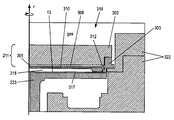
- FIG. 3 illustrates a cross section of the pedestal module and the showerhead module arranged in accordance with embodiments disclosed herein.
- FIG. 4 illustrates a cross section of a showerhead module arranged in accordance with an embodiment disclosed herein.
- FIG. 5 is a graph of surface contamination versus ALD SiN accumulation for eight chamber conditions.
- Front-end-of-line (FEOL) films have stringent in-film metals requirements since these films are deposited in close proximity to the active area of the device.
- Typical FEOL in-film metals specs are ⁇ 1 ⁇ 1010 atoms/cm 2 for most metals, including aluminum (Al).
- ALD atomic layer deposition
- silicon nitride films only halide-based silicon precursors have the reactivity required to make manufacturable films for most applications.
- Halide-based chemistry in general, and chlorine based (Cl-based) silicon precursors in particular, will attack Al chamber parts and make volatile byproducts, such as AlCl 3 at temperatures >150° C., that can be incorporated into the film.
- the chamber components near the semiconductor substrate (wafer) that will be exposed to halide chemistry are made of ceramic material such as aluminum nitride (AlN) to prevent Al corrosion.
- AlN ceramic in the as-received state is inert to halide-based chemistries
- AlN exposed to NF 3 -based chamber cleans will have Al-containing compounds generated on the surface during chamber cleaning that will subsequently be attacked by halide-based chemistry, generating volatile Al compounds that are incorporated in the film deposited on the semiconductor substrates.
- ALD SiN pre-coat For Cl-based ALD nitride film formation, post-clean reactive surface compounds can eventually be covered up by a time consuming ALD SiN pre-coat that eventually drops the in-film Al concentration below the specified limit.
- the amount of ALD SiN pre-coat required is not very repeatable and can take over 48 hours of deposition time to get to a point where the in-film metals meet specified limits and product wafers can finally be processed. This approach is too long and unrepeatable for a production environment, and severely limits the number of wafers that can be processed metals-free before the accumulation limit is reached and another chamber clean needs to be run.
- a method has been developed which can be used with Lam Research Corporation's Striker NitrideTM virtual seal chamber design, which enables deposition of high-throughput ALD SiN films that meet FEOL metals requirements repeatably, without the need for excessive ALD SiN pre-coats.
- the method for high-temperature halide-based ALD SiN processes is to drop the pedestal temperature to ⁇ 400° C., run the NF 3 -based clean, ramp the temperature back up to process temperature, and coat the chamber interior surfaces with a halide-free, fast ALD oxide undercoat. Running the chamber clean at temperatures of 400° C.
- halide-free ALD oxide undercoat on the order of 2,000 ⁇ or less, preferably about 1,000 ⁇ or less. Since the ALD oxide process is fast, a 1,000 ⁇ undercoat can be deposited in 1 to 11 ⁇ 2 hours, which is a tolerable amount of time for ALD SiN since chamber cleans would only be run every 3-4 days in production.
- the choice of a halide-free ALD oxide undercoat is the result of experimentally testing a selection of alternate undercoats, such as PECVD oxide and halide-based ALD oxide. The results of the tests show that only a highly conformal, fast, halide-free ALD oxide film successfully meets the requirements of very low post-clean metals in a manufacturable way.
- the Striker NitrideTM virtual seal design provides a small volume processing region (micro-volume) which contains the gases and byproducts produced during the cleaning, undercoating, pre-coating and silicon nitride deposition steps.
- the deposition and clean chemistry reactants can be confined to the wafer cavity, which can be coated completely with an ALD oxide undercoat.
- This containment is useful for temporal ALD since pressure cycling is used in between dose and conversion half-reaction cycles to ensure the respective chemistries do not mix.
- This pressure cycling introduces multiple AlCl 3 transport modes that demand the reactive chemistry be contained in order to suppress metals incorporation into the SiN film.
- the method is useful for halide-based ALD SiN processes deposited at a temperature less than 400° C.
- a non-halide ALD oxide undercoat can prove useful for suppressing metals in PECVD reactors as well, since the undercoat testing clearly showed that PECVD oxide undercoats were inferior in terms of covering potential metals sources.
- the method disclosed herein provides a needed solution for temporal ALD single-wafer systems which, in general, require frequent, periodic NF 3 -based cleans.
- Temporal reactors are so named because the wafers are stationary, but the half-reaction gases toggle back in forth with time.
- the time to toggle gases is short relative to the dose and conversion half-reaction times.
- the gases are always on, but the wafers are moved through the dedicated, isolated volumes on a carousel. The speed with which the wafers can move is determined by the reaction kinetics.
- Spatial ALD mini-batch systems can avoid NF 3 -based cleans since each half-reaction is confined to a dedicated chamber volume.
- Furnace ALD systems can use quartz components to eliminate metals sources since they do not need to run frequent NF 3 -based chamber cleans. Their isothermal design allows them to build up deposition on the walls until a system performance maintenance treatment is required, usually months apart.
- temporal single-wafer ALD reactors can provide, such as axi-symmetric thickness profiles, lower chemical consumption, higher throughput for kinetically slow processes like SiN, uniform center-to-edge sidewall thickness on high aspect ratio features due to uniform chemical flux across the wafer, lower thermal budget, and graded film capability enabled through variable deposition temperature.
- the Striker NitrideTM system enables the use of halide-based chemistry to deposit fast, conformal AlD SiN films in a temporal, single-wafer plasma enhanced atomic layer deposition (PEALD) tool.
- PEALD plasma enhanced atomic layer deposition
- a temporal ALD reactor there is film formation on the walls and the wafer cavity must be cleaned with NF 3 -based chemistry more frequently than the above-mentioned technologies.
- the high post-clean metals issue must be overcome in a way that does not lower throughput and increase the cost of ownership to such an extent that the overall process is not manufacturable.
- ALD oxide has fast kinetics which enable short cycle times and high deposition rates, which greatly reduce the undercoating time required to coat the wafer cavity.
- the Striker NitrideTM virtual seal design is advantageous in that it contains the deposition chemistry during pressure cycling to a region that can be thoroughly coated with the non-halide ALD oxide undercoat.
- the method described herein is highly advantageous for deposition systems having a non-metallic (ceramic) chamber-in-chamber design.
- a non-metallic (ceramic) chamber-in-chamber design By providing such systems with an in situ, 100% conformal undercoat, it is possible to carry out repeated reduced-temperature in situ deposition/clean cycles prior to processing substrates with halide-based SiN chemistry.
- the combination of chemistry containment hardware and a fast, conformal, in situ non-halide ALD oxide undercoat for ALD SiN metals suppression offers low cost-of-ownership and materials flexibility compared to other alternatives. Time consuming ALD SiN pre-coats, which can take 48-72 hours, depending on chemistry, can severely limit tool availability.
- PECVD oxide undercoats have low conformality and cannot provide coverage of the highly irregular, rough surfaces of materials that are being attacked by clean chemistry.
- Protective liners can be used to protect chamber components from halide attack, but it is challenging, as well as expensive, to find liners/coatings that can survive thermal cycling and be resistant to halide deposition chemistry, NF 3 -based and O 2 -based cleans (needed for carbon-doped films).
- the method described herein improves uptime and cost-of-ownership further by eliminating the need for replaceable liners or frequent chamber openings to get rid of corrosive byproducts.
- the method described herein can be carried out in deposition chambers having various types of showerhead arrangements.
- there are two main types of deposition showerheads the chandelier type and the flush mount.
- the chandelier showerheads have a stem attached to the top of the chamber on one end and the faceplate on the other end, resembling a chandelier. A part of the stem may protrude the chamber top to enable connection of gas lines and RF power.
- the flush mount showerheads are integrated into the top of a chamber and do not have a stem.
- a flush mount type showerhead can be used for purposes of reducing chamber volume such as disclosed in commonly-assigned U.S. Published Applications 2015/0004798 and 2015/0011096, the entire disclosures of which are hereby incorporated by reference.
- FIG. 1 is a schematic diagram showing an overview of a chemical deposition apparatus 201 in accordance with embodiments disclosed herein.
- a substrate 13 sits on top of a movable pedestal module 223 that can be raised or lowered relative to a showerhead module 211 , which may also be moved vertically.
- Reactant material gases are introduced into a processing zone 318 of the chamber via gas line 203 .
- the apparatus may be modified to have one or more gas lines, depending on the number of reactant gases used.
- the chamber is evacuated through vacuum lines 235 that are connected to a vacuum source 209 .
- the vacuum source may be a vacuum pump. By raising the pedestal, a micro-volume is located beneath showerhead module 211 .
- the micro-volume can range from 0.1 liter to 2 liters.
- the pedestal module can be raised or lowered to expose a substrate to the micro-volume and/or to vary a volume of the micro-volume.
- the pedestal module can be raised to position a substrate within the micro-volume such that the micro-volume completely encloses the substrate as well as a portion of the pedestal module.
- a position of the showerhead module could be adjusted relative to the pedestal module to vary a volume of microvolume.
- the apparatus 201 can be a multi-station apparatus having a plurality of micro-volumes.
- the outer chamber can have an internal volume of 180 L in which four pedestals can be raised in close proximity to four showerheads to provide four micro-volumes.
- FIG. 2 provides a simple block diagram depicting various apparatus components arranged for implementing embodiments disclosed herein wherein plasma is utilized to enhance deposition.
- a processing zone 318 serves to contain the plasma generated by a capacitively coupled plasma system including a showerhead module 211 working in conjunction with a pedestal module 223 , wherein the pedestal module 223 is heated.
- RF source(s) such as at least one high-frequency (HF) RF generator 204 , connected to a matching network 206 , and an optional low-frequency (LF) RF generator 202 are connected to the showerhead module 211 .
- the HF generator 204 can be connected to the pedestal module 223 .
- the power and frequency supplied by matching network 206 is sufficient to generate plasma from the process gas/vapor.
- both the HF generator and the LF generator are used, and in an alternate embodiment, just the HF generator is used.
- the HF generator is operated generally at frequencies of about 2-100 MHz; in a preferred embodiment at 13.56 MHz or 27 MHz.
- the LF generator is operated generally at about 50 kHz to 2 MHz; in a preferred embodiment at about 350 to 600 kHz.
- the process parameters may be scaled based on the chamber volume, substrate size, and other factors. Similarly, the flow rates of process gas may depend on the free volume of the vacuum chamber or processing zone.
- the pedestal module 223 supports a substrate 13 on which materials such as thin films may be deposited.
- the pedestal module 223 can include a fork or lift pins to hold and transfer the substrate during and between the deposition and/or plasma treatment reactions.
- the substrate 13 may be configured to rest on a surface of the pedestal module 223 , however in alternate embodiments the pedestal module 223 may include an electrostatic chuck, a mechanical chuck, or a vacuum chuck for holding the substrate 13 on the surface of the pedestal module 223 .
- the pedestal module 223 can be coupled with a heater block 220 for heating substrate 13 to a desired temperature. Generally, substrate 13 is maintained at a temperature of about 25° C. to 500° C. or greater depending on the material to be deposited.
- a system controller 228 is employed to control process conditions during deposition, post deposition treatments, and/or other process operations.
- the controller 228 will typically include one or more memory devices and one or more processors.
- the processor may include a CPU or computer, analog and/or digital input/output connections, stepper motor controller boards, etc.
- the controller 228 can be used to control all of the activities of the apparatus.
- the system controller 228 executes system control software including sets of instructions for controlling the timing of the processing operations, frequency and power of operations of the LF generator 202 and the HF generator 204 , flow rates and temperatures of precursors and inert gases and their relative mixing, temperature of the heater block 220 and showerhead module 211 , pressure of the chamber, and other parameters of a particular process.
- Other computer programs stored on memory devices associated with the controller may be employed in some embodiments.
- the user interface may include a display screen, graphical software displays of the apparatus and/or process conditions, and user input devices such as pointing devices, keyboards, touch screens, microphones, etc.
- a non-transitory computer machine-readable medium can comprise program instructions for control of the apparatus.
- the computer program code for controlling the processing operations can be written in any conventional computer readable programming language: for example, assembly language, C, C++, Pascal, Fortran or others. Compiled object code or script is executed by the processor to perform the tasks identified in the program.
- the controller parameters relate to process conditions such as, for example, timing of the processing steps, flow rates and temperatures of precursors and inert gases, temperature of the wafer, pressure of the chamber and other parameters of a particular process. These parameters are provided to the user in the form of a recipe, and may be entered utilizing the user interface.
- Signals for monitoring the process may be provided by analog and/or digital input connections of the system controller.
- the signals for controlling the process are output on the analog and digital output connections of the apparatus.
- the system software may be designed or configured in many different ways. For example, various chamber component subroutines or control objects may be written to control operation of the chamber components necessary to carry out deposition processes. Examples of programs or sections of programs for this purpose include substrate timing of the processing steps code, flow rates and temperatures of precursors and inert gases code, and a code for pressure of the chamber.
- FIG. 3 illustrates a cross section of a chemical isolation chamber 319 including the pedestal module 223 and the showerhead module 211 of FIGS. 1 and 2 in greater detail wherein the pedestal module 223 and showerhead module 211 form a cavity 318 in which a semiconductor substrate is processed.
- the cavity 318 is a micro-volume formed between the showerhead module 211 and the pedestal module 223 wherein a lower surface of a ceramic faceplate 301 of the showerhead module 211 forms an upper wall and a sidewall of the cavity 318 , and an upper surface of the pedestal module 223 forms a lower wall of the cavity 318 .
- An exemplary embodiment of a deposition apparatus which includes dual chamber seals can be found in commonly assigned U.S. Pat. No. 7,737,035, which is hereby incorporated by reference in its entirety.
- the pedestal module 223 includes a bottom RF electrode 317 and the substrate 13 sits on the pedestal module 223 .
- the bottom RF electrode 317 is grounded.
- the distance between the top of the substrate 13 and the bottom surface of the showerhead module 211 during processing is preferably about 5 to 16 millimeters.
- the pedestal module 223 includes a heater (see FIG. 2 ) and the faceplate 211 of the showerhead module 211 is heated from heat released from the pedestal module 223 during processing and by plasma struck in the cavity 318 during processing.
- the temperature inside the chamber may be maintained through a heating mechanism in the showerhead module 211 and the pedestal module 223 .
- the substrate 13 is located in an isothermal environment.
- An isothermal processing zone is formed by maintaining each exposed surface of the cavity 318 at a desired temperature.
- the isothermal processing zone allows the substrate 13 to be uniformly heated and maintained at a desired temperature so that an undesired temperature gradient is not formed across the substrate 13 .
- heat loss from the faceplate 301 to a backing plate 302 and heat loss from the faceplate 301 to an isolation ring 303 is minimized.
- the showerhead module 211 can be heated to greater than about 250° C.
- the pedestal module 223 can be heated to greater than about 250° C. to 500° C. or greater than about 500° C.
- each exposed surface of the cavity 318 is formed from a ceramic material such as aluminum nitride, aluminum oxide, silicon nitride, silicon carbide.
- the showerhead module 211 includes the faceplate 301 , the backing plate 302 , and the isolation ring 303 , wherein the isolation ring surrounds the faceplate 301 and the backing plate 302 and supports the backing plate 302 .
- the isolation ring 303 is preferably formed from a ceramic material such as aluminum oxide (Al 2 O 3 ) or aluminum nitride (AlN) and can be supported on a grounded chamber wall 322 of the chemical isolation chamber 319 .
- the backing plate 302 is formed from a metal material.
- the backing plate 302 can be formed from an aluminum alloy such as Al 6061 or stainless steel wherein the backing plate 302 can include a ceramic outer coating such as an aluminum oxide outer coating, a yttrium oxide outer coating, or a polymeric coating depending on the intended application.
- the backing plate 302 is RF hot, i.e., powered by an RF source.
- the backing plate 302 can be a cooled backing plate.
- the faceplate 301 is preferably formed from a ceramic material and in preferred embodiments can be formed from aluminum oxide (Al 2 O 3 ), or aluminum nitride (AlN).
- the faceplate 301 can include an RF electrode 310 embedded therein wherein the embedded RF electrode 310 is preferably a mesh electrode.
- a gas plenum 308 is formed between the faceplate 301 and the backing plate 302 .
- the height of the gas plenum 308 between the faceplate 301 and the backing plate 302 enables good gas flow from the plenum 308 to the cavity 318 while providing minimal plenum volume.
- the height of the plenum 308 is about 2 to 6 mm.
- At least one RF contact 312 electrically connects the backing plate 302 and the RF electrode 310 embedded in the faceplate 301 .
- the RF contact 312 can be an annular RF contact made of a metallic strip having at least one bend wherein the RF contact 312 forms an outer perimeter of the gas plenum 308 between the faceplate 301 and the backing plate 302 .
- the RF contact 312 forms a thermal choke between the faceplate 301 and the backing plate 302 .
- Examples of ceramic faceplates with embedded RF electrodes can be found in commonly-assigned U.S. Pat. No. 9,441,296 and commonly-assigned U.S. Published Application 2016/0203952.
- FIG. 4 illustrates an exemplary embodiment of a showerhead module 211 and substrate support 223 which form an isothermal processing zone wherein a support element 309 attaches a faceplate 301 of the showerhead module 211 to the backing plate 302 of the showerhead module.
- a support element 309 attaches a faceplate 301 of the showerhead module 211 to the backing plate 302 of the showerhead module.
- each surface which is exposed to the isothermal processing zone is a ceramic surface which is maintained at a desired temperature.
- the showerhead module 211 includes a faceplate 301 wherein a lower surface of the faceplate forms an upper wall of a cavity 318 and optionally a sidewall of the cavity 318 defining the isothermal processing zone, a backing plate 302 , and an isolation ring 303 , wherein the isolation ring 303 surrounds the faceplate 301 and the backing plate 302 .
- the backing plate 302 can include one or more gas inlets 305 and one or more gas outlets, and the faceplate 301 preferably includes a plurality of through holes 304 for delivering process gas to the isothermal processing zone, delivering inert gas to the isothermal processing zone, or removing process and/or inert gas from the isothermal processing zone.
- At least one compression seal can be located between the backing plate and the faceplate wherein each compression seal can form a boundary of at least one gas plenum.
- two compression seals can be used to form gas plenums wherein the first compression seal is a first annular lever seal 306 a which is compressed between the faceplate 301 and the backing plate 302 and wherein the first annular lever seal 306 a forms an inner gas plenum 308 a .
- the inner gas plenum 308 a can be in fluid communication with the one or more gas inlets 305 of the backing plate 302 and a plurality of the through holes 304 of the faceplate 301 such that a process gas can be delivered therethrough into the cavity 318 which defines the isothermal processing zone.
- the second compression seal can be a second annular lever seal 306 b which surrounds the first annular lever seal 306 a and is compressed between the faceplate 301 and the backing plate 302 wherein the second annular lever seal 306 a forms an intermediate plenum 308 b which surrounds the inner gas plenum 308 a .
- the intermediate plenum 308 b can be in fluid communication with the one or more gas outlets 315 of the backing plate 302 and a plurality of the through holes 304 of the faceplate 301 such that a process gas can be removed from the isothermal processing zone in cavity 318 by the vacuum source.
- an outer gas plenum 308 c surrounds the intermediate plenum 308 b .
- the outer gas plenum 308 c can deliver inert gas to a gap between the faceplate 301 and the isolation ring 303 which is in fluid communication with the isothermal processing zone in cavity 318 and wherein the isolation ring 303 forms an outer periphery of the outer gas plenum 308 c.
- the faceplate can include outlets for removing gases from the cavity 318 .
- the central zone of the faceplate which extends completely over the wafer can include concentric gas inlets and gas outlets to deliver process gas and withdraw reacted gas from the isothermal processing zone.
- a suitable arrangement of concentric inlets and outlets is disclosed in commonly-assigned U.S. Pat. No. 5,614,026, the disclosure of which is hereby incorporated by reference.
- the processing zone is preferably bounded by ceramic surfaces such as described above wherein the showerhead module 211 and substrate support 223 form an isothermal processing zone (micro-volume) in which each surface which is exposed to the isothermal processing zone is a ceramic surface which is maintained at a desired temperature.
- the showerhead module 211 includes a faceplate 301 wherein a lower surface of the faceplate forms an upper wall of a cavity 318 and optionally a sidewall of the cavity 318 defining the isothermal processing zone, a backing plate 302 , and an isolation ring 303 , wherein the isolation ring 303 surrounds the faceplate 301 and the backing plate 302 .
- the backing plate 302 can include one or more gas inlets and one or more gas outlets, and the faceplate 301 preferably includes a plurality of through holes 304 for delivering process gas to the isothermal processing zone, delivering inert gas to the isothermal processing zone, or removing process and/or inert gas from the isothermal processing zone.
- the chamber cleaning process can be carried out as described in commonly-assigned U.S. Published Application 2014/0053867, the disclosure of which is hereby incorporated by reference.
- the cleaning method may include one or more stages. For example, introducing the cleaning mixture into the deposition chamber, exposing the interior surfaces of the deposition chamber to the cleaning mixture and reacting the residue with the cleaning mixture may be performed at a chamber pressure of at least about 0.6 Torr during the first stage and no more than about 0.6 Torr during the second stage.
- the plasma energy during the first stage may be less than the plasma energy during the second stage. In certain embodiments, the plasma energy is delivered at about 1,000 W to 2,000 W during the first stage and at about 2,000 W to 3,000 W during the second stage.
- the cleaning reagents comprise an oxygen containing compound and a fluorine containing compound
- the oxygen containing compound can have a flow rate of at least ten times greater than a flow rate of the fluorine containing compound during the first stage and at least three times greater during the second stage.
- the fluorine containing compound can be NF 3 .
- the undercoating can be deposited as described in commonly-assigned U.S. Published Application 2015/0147482, the disclosure of which is hereby incorporated by reference.
- An undercoating is defined as a layer of film formed on the interior surfaces of the reaction chamber prior to processing substrates in the reaction chamber.
- An undercoating is distinct from film buildup that occurs during a normal deposition process where material is deposited on substrates. In contrast to buildup that occurs during deposition on substrates, an undercoating is generally deposited without any substrates present in a reaction chamber.
- an undercoating may be deposited directly on the ceramic chamber surfaces (e.g., on aluminum nitride or aluminum oxide) whereas film deposited during deposition on substrates is typically not in contact with these surfaces if it is deposited on top of a previously formed undercoating.
- a substrate is a solid piece of material that may be inserted and removed from the reaction chamber, which is not part of the reaction chamber, upon which film is deposited, and upon which film deposition is generally desired.
- a semiconductor wafer (with or without film(s) deposited thereon) is a typical substrate.
- substrates are disc-shaped and have a diameter of, for example, 200, 300 or 450 mm. Substrates typically go through many rounds of processing to become semiconductor devices.
- substrates are not intended to become fully functioning devices. These substrates may be referred to as dummy wafers, and they may be used as test vehicles for evaluating a deposition process or as sacrificial substrates for equilibrating a reaction chamber, for example. When depositing the undercoating, the substrate-free chamber allows the undercoating to uniformly coat the ceramic chamber surfaces.
- An undercoating is also distinct from a layer that may be deposited on chamber surfaces during certain test cycles, for example where a deposition process is run for a relatively small number of cycles without any substrates present.
- One difference is that the undercoating formation process is repeated many times to form a film of a desired minimum thickness. This minimum thickness is important in ensuring that the undercoat is able to function (e.g., minimize flaking and particle formation, and maximize uniformity) as desired.
- the reaction chamber is “clean” at the beginning of operation, i.e., there is no undercoating or other non-permanent deposited film present on the chamber surfaces.
- a halide-free silicon precursor such as silane and a nitrogen precursor such as nitrous oxide can be flowed into the reaction chamber at the same time.
- a plasma is ignited in the reaction chamber, driving a gas-phase reaction between the silane and oxygen to form ALD silicon oxide.
- the plasma is generated by an RF plasma generator, and the RF power used to drive the generator can be on the order of about 1000 to 3000 W (divided among four stations, depositing on 300 mm diameter substrates).
- the reaction chamber surfaces become coated with the undercoat film.
- the micro-volume ceramic surfaces are coated with the undercoating, i.e., the pedestal and showerhead surfaces enclosing the micro-volume.
- the reaction chamber can be purged/flushed multiple times to remove any unwanted reactants.
- the purge may include flowing gas that does not contain the species to be removed from the chamber. Alternatively or in addition, the purge may include evacuating the reaction chamber.
- Reactants used to deposit films on substrates can be flowed into the reaction chamber to pre-coat the chamber surfaces before any substrates are present in the reaction chamber.
- This pre-coating helps prime the gas delivery hardware (e.g., liquid chemical injectors, gas delivery lines, etc.) and other portions of the apparatus by exposing them to the reactants used during deposition.
- the pre-coating can be deposited with halide-free or halide containing reactants.
- the pre-coating can be deposited using the same reactants.
- Halide containing reactants are preferred for depositing ALD silicon nitride films since the films can be deposited at higher rates than halide-free reactants.
- a series of substrates can be sequentially processed in the reaction chamber after depositing the pre-coat over the undercoat.
- film is also deposited on the interior surfaces of the reaction chamber. This film builds up over the course of processing many substrates, and eventually begins to peel or flake off.
- the reaction chamber undergoes an in situ cleaning process to remove the deposited film and undercoat. This cleaning process is typically undertaken when no substrates are present in the reaction chamber.
- the chamber cleaning process may involve introducing a gas phase species, e.g., a fluorine-containing compound, which reacts with the deposited film to form a volatile product that may be purged from the chamber.
- the processing scheme may then be repeated on the newly cleaned chamber.
- the disclosed embodiments use a halide-free silicon oxide ALD undercoating prior to depositing silicon nitride films on substrates.
- the silicon oxide ALD undercoating is deposited using halogen-free reactants. Any appropriate halide-free silicon-containing reactant and oxidant may be used for the deposition of silicon oxide undercoating.
- the silicon-containing precursor may include, for example, a silane or an aminosilane.
- a silane contains hydrogen and/or carbon groups, but does not contain a halogen.
- silanes examples include silane (SiH 4 ), disilane (Si 2 H 6 ), and organo silanes such as methylsilane, ethylsilane, isopropylsilane, t-butylsilane, dimethylsilane, diethylsilane, di-t-butylsilane, allylsilane, sec-butylsilane, thexylsilane, isoamylsilane, t-butyldisilane, di-t-butyldisilane, and the like.
- An aminosilane includes at least one nitrogen atom bonded to a silicon atom, but may also contain hydrogens, oxygens, and carbons.
- aminosilanes are mono-, di-, tri- and tetra-aminosilane (H 3 Si(NH 2 ) 4 , H 2 SiNH 2 ) 2 , HSi(NH 2 ) 3 and Si(NH 2 ) 4 , respectively), as well as substituted mono-, di-, tri- and tetra-aminosilanes, for example, t-butylaminosilane, methylaminosilane, tert-butylsilanamine, bis(tertiarybutylamino)silane (SiH 2 (NHC(CH 3 ) 3 ) 2 (BTBAS), tert-butyl silylcarbamate, SiH(CH 3 )—(N(CH 3 ) 2 ) 2 , SiHCl—(N(CH 3 ) 2 ) 2 , (Si(CH 3 ) 2 NH) 3 and the like.
- a further example of an aminosilane is trisilylamine (N(SiH
- the silicon nitride film is deposited via ALD using a silicon-containing film precursor which is a compound and/or reagent containing silicon which may be used to form a silicon nitride film.
- the silicon-containing film precursor is preferably a halosilane such as an iodosilane, bromosilane, chlorosilane or fluorosilane.
- the chlorosilane can be monochlorosilane, dichlorosilane, tetrachlorosilane or hexachlorodisaline
- the iodosilane can be diiodosilane, triiodosilane or tetraiodosilane
- the bromosilane can be tetrabromosilane.
- the silicon nitride film can be deposited as described in commonly-assigned U.S. Pat. Nos. 8,592,328, 8,728,956, 9,070,555 and 9,214,333 and U.S. Published Application Nos. 2016/0148800 and 2016/0148806, the disclosures of which are hereby incorporated by reference.
- the silicon nitride film may be formed by reaction of a silicon-containing reactant and one or more of a nitrogen-containing reactant and/or a nitrogen-containing reactant blend.
- Example silicon-containing reactants include, but are not limited to, bis(tertiarybutylamino)silane (SiH 2 (NHC(CH 3 ) 3 ) 2 or BTBAS), dichlorosilane (SiH 2 Cl 2 ), and chlorosilane (SiH 3 Cl).
- Example nitrogen-containing reactants include, but are not limited to, ammonia, nitrogen, and tert-butyl amine ((CH 3 ) 3 CNH 2 or t-butyl amine).
- An example nitrogen-containing reactant blend includes, but is not limited to, a blend of nitrogen and hydrogen.
- the silicon nitride film can be deposited using a halosilane such as a chlorosilane selected from tetrachlorosilane (SiCl 4 ), trichlorosilane (HSiCl 3 ), chloroallylsilane, chloromethylsilane, dichloromethylsilane, chlorodimethylsilane, chloroethylsilane, t-butylchlorosilane, di-t-butylchlorosilane, chloroisopropylsilane, chloro-sec-butylsilane, t-butyldimethylchlorosilane, thexyldimethylchlorosilane, and the like.
- a halosilane such as a chlorosilane selected from tetrachlorosilane (SiCl 4 ), trichlorosilane (HSiCl 3 ), chloroallylsilane, chloromethyl
- the silicon nitride is preferably deposited by ALD, more preferably PEALD wherein a silicon-containing precursor is adsorbed onto an exposed surface of a semiconductor substrate supported on a pedestal of one of the stations, the silicon-containing precursor is purged from the station, a nitrogen plasma is exposed to the adsorbed silicon-containing precursor on the semiconductor substrate, and plasma is purged from the station.
- ALD atomic layer deposition
- PEALD PEALD
- the nitrogen plasma can be formed in-situ in which case the nitrogen plasma is formed directly above the substrate by igniting nitrogen gas into a plasma state inside the micro-volume or the nitrogen plasma can be formed remotely in which case nitrogen gas is ignited in a remote plasma generator upstream of the station.
- the plasma energy activates the nitrogen gas into ions and radicals, which react with the adsorbed layer of Si-containing precursor thereby forming silicon-nitrogen bonds and a thin film of silicon nitride.
- the purge steps can be carried out by stopping flow of the silicon-containing precursor and nitrogen gases and delivering a carrier gas into the micro-volume.
- the carrier gas can be supplied continuously throughout the ALD process or intermittently during the purge steps.
- Each deposition cycle of the ALD process can deposit a silicon nitride film having a thickness of about 0.05 ⁇ to about 3 ⁇ . For example, deposition at about 250° C. using disilane can deposit about 0.5 ⁇ per cycle.
- silicon nitride can be deposited by repeated cycles of delivering bis(diethyl)aminosilane with Ar carrier gas to a station, purging, igniting a nitrogen plasma, purging, to form a silicon nitride film of about 0.5 ⁇ in thickness each cycle.
- silicon nitride can be deposited by repeated cycles of delivering trisilylamine with Ar carrier gas to a station, purging, igniting a nitrogen or ammonia plasma, purging, to form a silicon nitride film of about 0.5 ⁇ in thickness each cycle.
- the semiconductor substrates can be coated with other film materials such as conductive and semiconductive materials.
- the film can be a nitride, oxide, carbide, boride, or other desired film material including but not limited to silicon oxide, oxynitride, doped oxide, doped silicate glass, undoped silicate glass(USG) such as boron doped silicate glass (BSG), phosphorus doped silicate glass (PSG), and boron phosphorus doped silicate glass (BPSG).
- BSG boron doped silicate glass
- PSG phosphorus doped silicate glass
- BPSG boron phosphorus doped silicate glass
- FIG. 5 shows surface concentration of Al versus ALD SiN accumulation for 8 chamber conditions (A-H) in which ALD silicon nitride is deposited at 475° C. using dichorosilane and NH 3 .
- Curve A illustrates surface contamination drops within desired specification limits after accumulation of about 500 ⁇ of ALD silicon nitride film on surfaces of a chamber which is not cleaned and there is no undercoat.
- Curve B illustrates surface contamination is above specification limits for a chamber which has been subjected to a 40 minute RF clean at 475° C. and there is no undercoat.
- Curve C illustrates that surface contamination is within specification limits after a 40 minute RF clean at 250° C. followed by deposition of 1000 ⁇ of a non-halide ALD silicon oxide undercoat.
- Curve D illustrates surface contamination is within specification limits after a 7.5 minute RF clean at 250° C. followed by deposition of 1000 ⁇ of a non-halide ALD silicon oxide undercoat.
- Curve E illustrates surface contamination is within specification limits after a 7.5 minute RF clean at 400° C. followed by deposition of 1000 ⁇ of a non-halide ALD silicon oxide undercoat.
- Curve F illustrates surface contamination is above specification limits after a 7.5 minute RF clean at 400° C. followed by deposition of 5 microns of a PECVD silicon oxide undercoat.
- Curve G illustrates surface contamination is above specification limits after a 7.5 minute RF clean at 400° C.
- Curve H illustrates surface contamination is above specification limits after a 7.5 minute RF clean at 400° C. followed by deposition of 1000 ⁇ of a halide (dichlorosilane and NH 3 ) ALD silicon oxide undercoat until silicon nitride buildup reaches about 1000 ⁇ .
Landscapes
- Chemical & Material Sciences (AREA)
- Engineering & Computer Science (AREA)
- Organic Chemistry (AREA)
- General Chemical & Material Sciences (AREA)
- Chemical Kinetics & Catalysis (AREA)
- Materials Engineering (AREA)
- Mechanical Engineering (AREA)
- Metallurgy (AREA)
- Plasma & Fusion (AREA)
- Physics & Mathematics (AREA)
- Analytical Chemistry (AREA)
- Inorganic Chemistry (AREA)
- Electromagnetism (AREA)
- Health & Medical Sciences (AREA)
- Epidemiology (AREA)
- Public Health (AREA)
- Chemical Vapour Deposition (AREA)
Abstract
A method of depositing ALD films on semiconductor substrates processed in a micro-volume of a plasma enhanced atomic layer deposition (PEALD) reaction chamber wherein a single semiconductor substrate is supported on a ceramic surface of a pedestal and process gas is introduced through gas outlets in a ceramic surface of a showerhead into a reaction zone above the semiconductor substrate, includes (a) cleaning the ceramic surfaces of the pedestal and showerhead with a fluorine plasma such that aluminum-rich byproducts are formed on the ceramic surfaces, (b) depositing a conformal halide-free atomic layer deposition (ALD) oxide undercoating on the ceramic surfaces so as to cover the aluminum-rich byproducts, (c) depositing a pre-coating on the halide-free ALD oxide undercoating, and (d) processing a batch of semiconductor substrates by transferring each semiconductor substrate into the reaction chamber and depositing a film on the semiconductor substrate supported on the ceramic surface of the pedestal.
Description
This application is a continuation application of U.S. patent application Ser. No. 15/287,176, filed Oct. 6, 2016, which will issue as U.S. Pat. No. 9,824,884 on Nov. 21, 2017, the contents of which is incorporated by reference herein in its entirety.
As the semiconductor industry advances, device dimensions are becoming increasingly smaller. These progressively smaller features require deposition procedures that are extremely uniform, as the presence of film impurities or other non-uniformities can often lead to the failure of a semiconductor device. An undercoat on interior chamber surfaces can help improve wafer-to-wafer thickness uniformity and within-wafer thickness uniformity.
Disclosed herein is a method of depositing silicon nitride films on a semiconductor substrate processed in a micro-volume of a plasma enhanced atomic layer deposition (PEALD) reaction chamber wherein the semiconductor substrate is supported on a ceramic surface of a pedestal and process gas is introduced through gas outlets in a ceramic surface of a showerhead into a reaction zone above the semiconductor substrate. The method includes cleaning the ceramic surfaces, depositing an undercoating on the ceramic surfaces, depositing a pre-coating over the undercoating, and sequentially processing a batch of semiconductor substrates in the processing region by transferring the semiconductor substrates one at a time into the processing region and depositing a silicon nitride film on each semiconductor substrate. After a predetermined number of semiconductor substrates are processed and/or film accumulation on the interior surfaces reaches a predetermined thickness, the cleaning, undercoating and pre-coating steps can be repeated before processing another batch of semiconductor substrates.
In one aspect of the embodiments herein, silicon nitride films are deposited on semiconductor substrates processed in a plasma enhanced atomic layer deposition (PEALD) reaction chamber wherein a single semiconductor substrate is supported on a ceramic surface of a pedestal and process gas is introduced through gas outlets in a ceramic surface of a showerhead into a reaction zone above the semiconductor substrate. The method comprises (a) cleaning the ceramic surfaces of the pedestal and showerhead with a fluorine plasma, (b) depositing a halide-free atomic layer deposition (ALD) oxide undercoating on the ceramic surfaces, (c) depositing a pre-coating of ALD silicon nitride on the halide-free ALD oxide undercoating, and (d) processing a batch of semiconductor substrates by sequentially transferring each semiconductor substrate into the reaction chamber and depositing a film of ALD silicon nitride on the semiconductor substrate supported on the ceramic surface of the pedestal.
In forming the undercoating, the method can be carried out by (i) introducing a flow of a halogen-free silicon-containing first reactant in vapor phase into the reaction chamber and allowing the first reactant to adsorb onto the ceramic surfaces of the reaction chamber; (ii) introducing a flow of an oxygen-containing second reactant in vapor phase into the reaction chamber while the first reactant is adsorbed on the ceramic surfaces of the reaction chamber; and (iii) exposing the reaction chamber to plasma when the flow of at least one of the first and second reactants has ceased, in order to drive a reaction between the first and second reactants on the ceramic surfaces of the reaction chamber to form the undercoating, where the undercoating conformally coats the ceramic surfaces of the reaction chamber; wherein operations (i)-(iii) occur when there is no semiconductor substrate present in the reaction chamber, and wherein operations (i)-(iii) are repeated until the undercoating is at least about 500 Å thick.
In accordance with another embodiment, films are deposited on semiconductor substrates processed in a micro-volume of a plasma enhanced atomic layer deposition (PEALD) reaction chamber wherein a single semiconductor substrate is supported on a ceramic surface of a pedestal and process gas is introduced through gas outlets in a ceramic surface of a showerhead into a reaction zone above the semiconductor substrate. The method comprises (a) cleaning the ceramic surfaces of the pedestal and showerhead with a fluorine plasma such that aluminum-rich byproducts are formed on the ceramic surfaces; (b) depositing a conformal halide-free atomic layer deposition (ALD) oxide undercoating on the ceramic surfaces so as to cover the aluminum-rich byproducts; (c) depositing a pre-coating on the halide-free ALD oxide undercoating; and (d) processing a batch of semiconductor substrates by transferring each semiconductor substrate into the reaction chamber and depositing a film on the semiconductor substrate supported on the ceramic surface of the pedestal.
The conformal halide-free ALD oxide undercoating can be formed by (i) introducing a flow of a halogen-free silicon-containing first reactant in vapor phase into the reaction chamber and allowing the first reactant to adsorb onto the interior surfaces of the reaction chamber; (ii) introducing a flow of an oxygen-containing second reactant in vapor phase into the reaction chamber while the first reactant is adsorbed on the interior surfaces of the reaction chamber; and (iii) exposing the reaction chamber to plasma when the flow of at least one of the first and second reactants has ceased, in order to drive a reaction between the first and second reactants on the interior surfaces of the reaction chamber to form the undercoating, where the undercoating conformally coats the interior surfaces of the reaction chamber; where operations (i)-(iii) occur when there is no substrate present in the reaction chamber, and where operations (i)-(iii) are repeated until the undercoating is at least about 500 Å thick. Preferably, the ceramic surfaces of the showerhead and pedestal are aluminum nitride, step (a) is carried out at with the pedestal and showerhead at a temperature below 400° C., and step (c) is carried out with the pedestal and showerhead at a temperature above 400° C. In addition, the undercoating can be deposited to a thickness of at least 500 Å, step (c) can be carried out with the pedestal and showerhead at a temperature of about 475° C. to about 635° C., and step (a) can be carried out with the pedestal and showerhead at a temperature below 300° C. Preferably, step (a) is carried out with NF3 energized into a plasma state upstream from the micro-volume using a remote inductively coupled plasma generator or by flowing NF3 into the micro-volume and energizing the NF3 into a plasma state within the micro-volume by applying RF power to an embedded RF electrode in the showerhead.
Front-end-of-line (FEOL) films have stringent in-film metals requirements since these films are deposited in close proximity to the active area of the device. Typical FEOL in-film metals specs are <1×10¹⁰ atoms/cm2 for most metals, including aluminum (Al). For high-throughput, high-conformality atomic layer deposition (ALD) silicon nitride films, only halide-based silicon precursors have the reactivity required to make manufacturable films for most applications.
Halide-based chemistry in general, and chlorine based (Cl-based) silicon precursors in particular, will attack Al chamber parts and make volatile byproducts, such as AlCl3 at temperatures >150° C., that can be incorporated into the film. For this reason, the chamber components near the semiconductor substrate (wafer) that will be exposed to halide chemistry are made of ceramic material such as aluminum nitride (AlN) to prevent Al corrosion. While AlN ceramic in the as-received state is inert to halide-based chemistries, AlN exposed to NF3-based chamber cleans will have Al-containing compounds generated on the surface during chamber cleaning that will subsequently be attacked by halide-based chemistry, generating volatile Al compounds that are incorporated in the film deposited on the semiconductor substrates.
For Cl-based ALD nitride film formation, post-clean reactive surface compounds can eventually be covered up by a time consuming ALD SiN pre-coat that eventually drops the in-film Al concentration below the specified limit. Unfortunately, the amount of ALD SiN pre-coat required is not very repeatable and can take over 48 hours of deposition time to get to a point where the in-film metals meet specified limits and product wafers can finally be processed. This approach is too long and unrepeatable for a production environment, and severely limits the number of wafers that can be processed metals-free before the accumulation limit is reached and another chamber clean needs to be run.
As disclosed herein, a method has been developed which can be used with Lam Research Corporation's Striker Nitride™ virtual seal chamber design, which enables deposition of high-throughput ALD SiN films that meet FEOL metals requirements repeatably, without the need for excessive ALD SiN pre-coats. The method for high-temperature halide-based ALD SiN processes, with a typical pedestal temperature of 475° C. to 635° C., is to drop the pedestal temperature to <400° C., run the NF3-based clean, ramp the temperature back up to process temperature, and coat the chamber interior surfaces with a halide-free, fast ALD oxide undercoat. Running the chamber clean at temperatures of 400° C. or less slows the kinetics of the NF3 reaction with AlN enough so that the amount of Al-containing byproducts generated is held to a level that can be covered with a reasonable amount of halide-free ALD oxide undercoat on the order of 2,000 Å or less, preferably about 1,000 Å or less. Since the ALD oxide process is fast, a 1,000 Å undercoat can be deposited in 1 to 1½ hours, which is a tolerable amount of time for ALD SiN since chamber cleans would only be run every 3-4 days in production. The choice of a halide-free ALD oxide undercoat is the result of experimentally testing a selection of alternate undercoats, such as PECVD oxide and halide-based ALD oxide. The results of the tests show that only a highly conformal, fast, halide-free ALD oxide film successfully meets the requirements of very low post-clean metals in a manufacturable way.
The Striker Nitride™ virtual seal design provides a small volume processing region (micro-volume) which contains the gases and byproducts produced during the cleaning, undercoating, pre-coating and silicon nitride deposition steps. The deposition and clean chemistry reactants can be confined to the wafer cavity, which can be coated completely with an ALD oxide undercoat. This containment is useful for temporal ALD since pressure cycling is used in between dose and conversion half-reaction cycles to ensure the respective chemistries do not mix. This pressure cycling introduces multiple AlCl3 transport modes that demand the reactive chemistry be contained in order to suppress metals incorporation into the SiN film. The method is useful for halide-based ALD SiN processes deposited at a temperature less than 400° C. as well, since post-clean metals testing showed that Al-containing byproducts are still generated at clean temperatures of 250° C. or less. A non-halide ALD oxide undercoat can prove useful for suppressing metals in PECVD reactors as well, since the undercoat testing clearly showed that PECVD oxide undercoats were inferior in terms of covering potential metals sources.
The method disclosed herein provides a needed solution for temporal ALD single-wafer systems which, in general, require frequent, periodic NF3-based cleans. Temporal reactors are so named because the wafers are stationary, but the half-reaction gases toggle back in forth with time. For processes with relatively slow kinetics, like ALD SiN, the time to toggle gases is short relative to the dose and conversion half-reaction times. In a spatial reactor, the gases are always on, but the wafers are moved through the dedicated, isolated volumes on a carousel. The speed with which the wafers can move is determined by the reaction kinetics. Spatial ALD mini-batch systems can avoid NF3-based cleans since each half-reaction is confined to a dedicated chamber volume. This avoids film formation on the walls of the isolated chamber and obviates the need for frequent NF3 chamber cleans. Furnace ALD systems can use quartz components to eliminate metals sources since they do not need to run frequent NF3-based chamber cleans. Their isothermal design allows them to build up deposition on the walls until a system performance maintenance treatment is required, usually months apart. While furnace ALD and spatial mini-batch ALD systems can avoid post-NF3 clean metals contamination, these reactors cannot exploit the benefits that temporal single-wafer ALD reactors can provide, such as axi-symmetric thickness profiles, lower chemical consumption, higher throughput for kinetically slow processes like SiN, uniform center-to-edge sidewall thickness on high aspect ratio features due to uniform chemical flux across the wafer, lower thermal budget, and graded film capability enabled through variable deposition temperature.
The Striker Nitride™ system enables the use of halide-based chemistry to deposit fast, conformal AlD SiN films in a temporal, single-wafer plasma enhanced atomic layer deposition (PEALD) tool. With a temporal ALD reactor, there is film formation on the walls and the wafer cavity must be cleaned with NF3-based chemistry more frequently than the above-mentioned technologies. In order to take advantage of the many benefits of temporal ALD, the high post-clean metals issue must be overcome in a way that does not lower throughput and increase the cost of ownership to such an extent that the overall process is not manufacturable. These problems are overcome by combining a lower-temperature clean with a non-halide ALD oxide undercoat to enable metals-free ALD SiN wafer processing in a temporal reactor with minimal non-value-added overhead time. Lowering the clean temperature is desirable in order to slow down corrosion reactions between NF3 and AlN. Since halide chemistry will react with these Al-containing corrosion byproducts, a non-halide ALD oxide undercoat can be used to suppress AlXy formation while covering up all the surfaces that will be exposed to the halide-based deposition chemistry. ALD oxide is beneficial because it is 100% conformal and will cover all surface irregularities in the wafer cavity—including faceplate and lift-pin holes. In addition, ALD oxide has fast kinetics which enable short cycle times and high deposition rates, which greatly reduce the undercoating time required to coat the wafer cavity. The Striker Nitride™ virtual seal design is advantageous in that it contains the deposition chemistry during pressure cycling to a region that can be thoroughly coated with the non-halide ALD oxide undercoat.
The method described herein is highly advantageous for deposition systems having a non-metallic (ceramic) chamber-in-chamber design. By providing such systems with an in situ, 100% conformal undercoat, it is possible to carry out repeated reduced-temperature in situ deposition/clean cycles prior to processing substrates with halide-based SiN chemistry. For a single wafer temporal tool, the combination of chemistry containment hardware and a fast, conformal, in situ non-halide ALD oxide undercoat for ALD SiN metals suppression offers low cost-of-ownership and materials flexibility compared to other alternatives. Time consuming ALD SiN pre-coats, which can take 48-72 hours, depending on chemistry, can severely limit tool availability. PECVD oxide undercoats have low conformality and cannot provide coverage of the highly irregular, rough surfaces of materials that are being attacked by clean chemistry. Protective liners can be used to protect chamber components from halide attack, but it is challenging, as well as expensive, to find liners/coatings that can survive thermal cycling and be resistant to halide deposition chemistry, NF3-based and O2-based cleans (needed for carbon-doped films). Thus, the method described herein improves uptime and cost-of-ownership further by eliminating the need for replaceable liners or frequent chamber openings to get rid of corrosive byproducts.
The method described herein can be carried out in deposition chambers having various types of showerhead arrangements. In general, there are two main types of deposition showerheads, the chandelier type and the flush mount. The chandelier showerheads have a stem attached to the top of the chamber on one end and the faceplate on the other end, resembling a chandelier. A part of the stem may protrude the chamber top to enable connection of gas lines and RF power. The flush mount showerheads are integrated into the top of a chamber and do not have a stem. In a preferred embodiment, a flush mount type showerhead can be used for purposes of reducing chamber volume such as disclosed in commonly-assigned U.S. Published Applications 2015/0004798 and 2015/0011096, the entire disclosures of which are hereby incorporated by reference.
Within the chamber, the pedestal module 223 supports a substrate 13 on which materials such as thin films may be deposited. The pedestal module 223 can include a fork or lift pins to hold and transfer the substrate during and between the deposition and/or plasma treatment reactions. In an embodiment, the substrate 13 may be configured to rest on a surface of the pedestal module 223, however in alternate embodiments the pedestal module 223 may include an electrostatic chuck, a mechanical chuck, or a vacuum chuck for holding the substrate 13 on the surface of the pedestal module 223. The pedestal module 223 can be coupled with a heater block 220 for heating substrate 13 to a desired temperature. Generally, substrate 13 is maintained at a temperature of about 25° C. to 500° C. or greater depending on the material to be deposited.
In certain embodiments, a system controller 228 is employed to control process conditions during deposition, post deposition treatments, and/or other process operations. The controller 228 will typically include one or more memory devices and one or more processors. The processor may include a CPU or computer, analog and/or digital input/output connections, stepper motor controller boards, etc.
The controller 228 can be used to control all of the activities of the apparatus. The system controller 228 executes system control software including sets of instructions for controlling the timing of the processing operations, frequency and power of operations of the LF generator 202 and the HF generator 204, flow rates and temperatures of precursors and inert gases and their relative mixing, temperature of the heater block 220 and showerhead module 211, pressure of the chamber, and other parameters of a particular process. Other computer programs stored on memory devices associated with the controller may be employed in some embodiments.
Typically there will be a user interface associated with controller 228. The user interface may include a display screen, graphical software displays of the apparatus and/or process conditions, and user input devices such as pointing devices, keyboards, touch screens, microphones, etc.
A non-transitory computer machine-readable medium can comprise program instructions for control of the apparatus. The computer program code for controlling the processing operations can be written in any conventional computer readable programming language: for example, assembly language, C, C++, Pascal, Fortran or others. Compiled object code or script is executed by the processor to perform the tasks identified in the program.
The controller parameters relate to process conditions such as, for example, timing of the processing steps, flow rates and temperatures of precursors and inert gases, temperature of the wafer, pressure of the chamber and other parameters of a particular process. These parameters are provided to the user in the form of a recipe, and may be entered utilizing the user interface.
Signals for monitoring the process may be provided by analog and/or digital input connections of the system controller. The signals for controlling the process are output on the analog and digital output connections of the apparatus.
The system software may be designed or configured in many different ways. For example, various chamber component subroutines or control objects may be written to control operation of the chamber components necessary to carry out deposition processes. Examples of programs or sections of programs for this purpose include substrate timing of the processing steps code, flow rates and temperatures of precursors and inert gases code, and a code for pressure of the chamber.
The pedestal module 223 includes a bottom RF electrode 317 and the substrate 13 sits on the pedestal module 223. Preferably the bottom RF electrode 317 is grounded. The distance between the top of the substrate 13 and the bottom surface of the showerhead module 211 during processing is preferably about 5 to 16 millimeters. The pedestal module 223 includes a heater (see FIG. 2 ) and the faceplate 211 of the showerhead module 211 is heated from heat released from the pedestal module 223 during processing and by plasma struck in the cavity 318 during processing. In some embodiments, the temperature inside the chamber may be maintained through a heating mechanism in the showerhead module 211 and the pedestal module 223. Preferably, the substrate 13 is located in an isothermal environment. An isothermal processing zone is formed by maintaining each exposed surface of the cavity 318 at a desired temperature. The isothermal processing zone allows the substrate 13 to be uniformly heated and maintained at a desired temperature so that an undesired temperature gradient is not formed across the substrate 13. To form the isothermal processing zone, heat loss from the faceplate 301 to a backing plate 302 and heat loss from the faceplate 301 to an isolation ring 303 is minimized. In an embodiment, the showerhead module 211 can be heated to greater than about 250° C., and/or the pedestal module 223 can be heated to greater than about 250° C. to 500° C. or greater than about 500° C. In a preferred embodiment, each exposed surface of the cavity 318 is formed from a ceramic material such as aluminum nitride, aluminum oxide, silicon nitride, silicon carbide.
The showerhead module 211 includes the faceplate 301, the backing plate 302, and the isolation ring 303, wherein the isolation ring surrounds the faceplate 301 and the backing plate 302 and supports the backing plate 302. The isolation ring 303 is preferably formed from a ceramic material such as aluminum oxide (Al2O3) or aluminum nitride (AlN) and can be supported on a grounded chamber wall 322 of the chemical isolation chamber 319.
The backing plate 302 is formed from a metal material. For example the backing plate 302 can be formed from an aluminum alloy such as Al 6061 or stainless steel wherein the backing plate 302 can include a ceramic outer coating such as an aluminum oxide outer coating, a yttrium oxide outer coating, or a polymeric coating depending on the intended application. In a preferred embodiment, the backing plate 302 is RF hot, i.e., powered by an RF source. In an embodiment, the backing plate 302 can be a cooled backing plate. The faceplate 301 is preferably formed from a ceramic material and in preferred embodiments can be formed from aluminum oxide (Al2O3), or aluminum nitride (AlN). The faceplate 301 can include an RF electrode 310 embedded therein wherein the embedded RF electrode 310 is preferably a mesh electrode. A gas plenum 308 is formed between the faceplate 301 and the backing plate 302. Preferably the height of the gas plenum 308 between the faceplate 301 and the backing plate 302 enables good gas flow from the plenum 308 to the cavity 318 while providing minimal plenum volume. Preferably the height of the plenum 308 is about 2 to 6 mm. At least one RF contact 312 electrically connects the backing plate 302 and the RF electrode 310 embedded in the faceplate 301. In an embodiment, the RF contact 312 can be an annular RF contact made of a metallic strip having at least one bend wherein the RF contact 312 forms an outer perimeter of the gas plenum 308 between the faceplate 301 and the backing plate 302. Preferably the RF contact 312 forms a thermal choke between the faceplate 301 and the backing plate 302. Examples of ceramic faceplates with embedded RF electrodes can be found in commonly-assigned U.S. Pat. No. 9,441,296 and commonly-assigned U.S. Published Application 2016/0203952.
The faceplate can include outlets for removing gases from the cavity 318. For example, the central zone of the faceplate which extends completely over the wafer can include concentric gas inlets and gas outlets to deliver process gas and withdraw reacted gas from the isothermal processing zone. A suitable arrangement of concentric inlets and outlets is disclosed in commonly-assigned U.S. Pat. No. 5,614,026, the disclosure of which is hereby incorporated by reference.
Processing Zone Bounded by Ceramic Surfaces
The processing zone is preferably bounded by ceramic surfaces such as described above wherein the showerhead module 211 and substrate support 223 form an isothermal processing zone (micro-volume) in which each surface which is exposed to the isothermal processing zone is a ceramic surface which is maintained at a desired temperature. In an embodiment, the showerhead module 211 includes a faceplate 301 wherein a lower surface of the faceplate forms an upper wall of a cavity 318 and optionally a sidewall of the cavity 318 defining the isothermal processing zone, a backing plate 302, and an isolation ring 303, wherein the isolation ring 303 surrounds the faceplate 301 and the backing plate 302. The backing plate 302 can include one or more gas inlets and one or more gas outlets, and the faceplate 301 preferably includes a plurality of through holes 304 for delivering process gas to the isothermal processing zone, delivering inert gas to the isothermal processing zone, or removing process and/or inert gas from the isothermal processing zone.
Chamber Cleaning Process
The chamber cleaning process can be carried out as described in commonly-assigned U.S. Published Application 2014/0053867, the disclosure of which is hereby incorporated by reference. The cleaning method may include one or more stages. For example, introducing the cleaning mixture into the deposition chamber, exposing the interior surfaces of the deposition chamber to the cleaning mixture and reacting the residue with the cleaning mixture may be performed at a chamber pressure of at least about 0.6 Torr during the first stage and no more than about 0.6 Torr during the second stage. The plasma energy during the first stage may be less than the plasma energy during the second stage. In certain embodiments, the plasma energy is delivered at about 1,000 W to 2,000 W during the first stage and at about 2,000 W to 3,000 W during the second stage. In the embodiments where the cleaning reagents comprise an oxygen containing compound and a fluorine containing compound, the oxygen containing compound can have a flow rate of at least ten times greater than a flow rate of the fluorine containing compound during the first stage and at least three times greater during the second stage. The fluorine containing compound can be NF3.
ALD Undercoat
The undercoating can be deposited as described in commonly-assigned U.S. Published Application 2015/0147482, the disclosure of which is hereby incorporated by reference. An undercoating is defined as a layer of film formed on the interior surfaces of the reaction chamber prior to processing substrates in the reaction chamber. An undercoating is distinct from film buildup that occurs during a normal deposition process where material is deposited on substrates. In contrast to buildup that occurs during deposition on substrates, an undercoating is generally deposited without any substrates present in a reaction chamber. Further, an undercoating may be deposited directly on the ceramic chamber surfaces (e.g., on aluminum nitride or aluminum oxide) whereas film deposited during deposition on substrates is typically not in contact with these surfaces if it is deposited on top of a previously formed undercoating. A substrate is a solid piece of material that may be inserted and removed from the reaction chamber, which is not part of the reaction chamber, upon which film is deposited, and upon which film deposition is generally desired. In the context of semiconductor device fabrication, a semiconductor wafer (with or without film(s) deposited thereon) is a typical substrate. In many cases, substrates are disc-shaped and have a diameter of, for example, 200, 300 or 450 mm. Substrates typically go through many rounds of processing to become semiconductor devices. Certain other substrates, however, are not intended to become fully functioning devices. These substrates may be referred to as dummy wafers, and they may be used as test vehicles for evaluating a deposition process or as sacrificial substrates for equilibrating a reaction chamber, for example. When depositing the undercoating, the substrate-free chamber allows the undercoating to uniformly coat the ceramic chamber surfaces.
An undercoating is also distinct from a layer that may be deposited on chamber surfaces during certain test cycles, for example where a deposition process is run for a relatively small number of cycles without any substrates present. One difference is that the undercoating formation process is repeated many times to form a film of a desired minimum thickness. This minimum thickness is important in ensuring that the undercoat is able to function (e.g., minimize flaking and particle formation, and maximize uniformity) as desired.
In a typical processing scheme, the reaction chamber is “clean” at the beginning of operation, i.e., there is no undercoating or other non-permanent deposited film present on the chamber surfaces. During the undercoat deposition process, a halide-free silicon precursor such as silane and a nitrogen precursor such as nitrous oxide can be flowed into the reaction chamber at the same time. A plasma is ignited in the reaction chamber, driving a gas-phase reaction between the silane and oxygen to form ALD silicon oxide. In some cases, the plasma is generated by an RF plasma generator, and the RF power used to drive the generator can be on the order of about 1000 to 3000 W (divided among four stations, depositing on 300 mm diameter substrates). The reaction chamber surfaces become coated with the undercoat film. Preferably, only the micro-volume ceramic surfaces are coated with the undercoating, i.e., the pedestal and showerhead surfaces enclosing the micro-volume. The reaction chamber can be purged/flushed multiple times to remove any unwanted reactants. The purge may include flowing gas that does not contain the species to be removed from the chamber. Alternatively or in addition, the purge may include evacuating the reaction chamber.
Pre-Coat
Reactants used to deposit films on substrates can be flowed into the reaction chamber to pre-coat the chamber surfaces before any substrates are present in the reaction chamber. This pre-coating helps prime the gas delivery hardware (e.g., liquid chemical injectors, gas delivery lines, etc.) and other portions of the apparatus by exposing them to the reactants used during deposition. The pre-coating can be deposited with halide-free or halide containing reactants. For example, when depositing silicon nitride on semiconductor substrates, the pre-coating can be deposited using the same reactants. Halide containing reactants are preferred for depositing ALD silicon nitride films since the films can be deposited at higher rates than halide-free reactants.
Silicon Nitride ALD on Semiconductor Substrates
A series of substrates can be sequentially processed in the reaction chamber after depositing the pre-coat over the undercoat. As films are deposited on the substrates, film is also deposited on the interior surfaces of the reaction chamber. This film builds up over the course of processing many substrates, and eventually begins to peel or flake off. Then, after the substrates are processed, the reaction chamber undergoes an in situ cleaning process to remove the deposited film and undercoat. This cleaning process is typically undertaken when no substrates are present in the reaction chamber. Preferably, the chamber cleaning process may involve introducing a gas phase species, e.g., a fluorine-containing compound, which reacts with the deposited film to form a volatile product that may be purged from the chamber. The processing scheme may then be repeated on the newly cleaned chamber.
Silicon-Containing Precursors
The disclosed embodiments use a halide-free silicon oxide ALD undercoating prior to depositing silicon nitride films on substrates. The silicon oxide ALD undercoating is deposited using halogen-free reactants. Any appropriate halide-free silicon-containing reactant and oxidant may be used for the deposition of silicon oxide undercoating. The silicon-containing precursor may include, for example, a silane or an aminosilane. A silane contains hydrogen and/or carbon groups, but does not contain a halogen. Examples of silanes are silane (SiH4), disilane (Si2H6), and organo silanes such as methylsilane, ethylsilane, isopropylsilane, t-butylsilane, dimethylsilane, diethylsilane, di-t-butylsilane, allylsilane, sec-butylsilane, thexylsilane, isoamylsilane, t-butyldisilane, di-t-butyldisilane, and the like. An aminosilane includes at least one nitrogen atom bonded to a silicon atom, but may also contain hydrogens, oxygens, and carbons. Examples of aminosilanes are mono-, di-, tri- and tetra-aminosilane (H3Si(NH2)4, H2SiNH2)2, HSi(NH2)3 and Si(NH2)4, respectively), as well as substituted mono-, di-, tri- and tetra-aminosilanes, for example, t-butylaminosilane, methylaminosilane, tert-butylsilanamine, bis(tertiarybutylamino)silane (SiH2(NHC(CH3)3)2 (BTBAS), tert-butyl silylcarbamate, SiH(CH3)—(N(CH3)2)2, SiHCl—(N(CH3)2)2, (Si(CH3)2NH)3 and the like. A further example of an aminosilane is trisilylamine (N(SiH3)3).
Silicon Nitride Film
The silicon nitride film is deposited via ALD using a silicon-containing film precursor which is a compound and/or reagent containing silicon which may be used to form a silicon nitride film. The silicon-containing film precursor is preferably a halosilane such as an iodosilane, bromosilane, chlorosilane or fluorosilane. For example, the chlorosilane can be monochlorosilane, dichlorosilane, tetrachlorosilane or hexachlorodisaline, the iodosilane can be diiodosilane, triiodosilane or tetraiodosilane and the bromosilane can be tetrabromosilane.
The silicon nitride film can be deposited as described in commonly-assigned U.S. Pat. Nos. 8,592,328, 8,728,956, 9,070,555 and 9,214,333 and U.S. Published Application Nos. 2016/0148800 and 2016/0148806, the disclosures of which are hereby incorporated by reference. For example, the silicon nitride film may be formed by reaction of a silicon-containing reactant and one or more of a nitrogen-containing reactant and/or a nitrogen-containing reactant blend.
Example silicon-containing reactants include, but are not limited to, bis(tertiarybutylamino)silane (SiH2(NHC(CH3)3)2 or BTBAS), dichlorosilane (SiH2Cl2), and chlorosilane (SiH3Cl). Example nitrogen-containing reactants include, but are not limited to, ammonia, nitrogen, and tert-butyl amine ((CH3)3CNH2 or t-butyl amine). An example nitrogen-containing reactant blend, includes, but is not limited to, a blend of nitrogen and hydrogen. Alternatively, the silicon nitride film can be deposited using a halosilane such as a chlorosilane selected from tetrachlorosilane (SiCl4), trichlorosilane (HSiCl3), chloroallylsilane, chloromethylsilane, dichloromethylsilane, chlorodimethylsilane, chloroethylsilane, t-butylchlorosilane, di-t-butylchlorosilane, chloroisopropylsilane, chloro-sec-butylsilane, t-butyldimethylchlorosilane, thexyldimethylchlorosilane, and the like.
The silicon nitride is preferably deposited by ALD, more preferably PEALD wherein a silicon-containing precursor is adsorbed onto an exposed surface of a semiconductor substrate supported on a pedestal of one of the stations, the silicon-containing precursor is purged from the station, a nitrogen plasma is exposed to the adsorbed silicon-containing precursor on the semiconductor substrate, and plasma is purged from the station. The stations can be located in a vacuum chamber body which maintains a low pressure environment in all stations.
The nitrogen plasma can be formed in-situ in which case the nitrogen plasma is formed directly above the substrate by igniting nitrogen gas into a plasma state inside the micro-volume or the nitrogen plasma can be formed remotely in which case nitrogen gas is ignited in a remote plasma generator upstream of the station. The plasma energy activates the nitrogen gas into ions and radicals, which react with the adsorbed layer of Si-containing precursor thereby forming silicon-nitrogen bonds and a thin film of silicon nitride. The purge steps can be carried out by stopping flow of the silicon-containing precursor and nitrogen gases and delivering a carrier gas into the micro-volume. The carrier gas can be supplied continuously throughout the ALD process or intermittently during the purge steps. Each deposition cycle of the ALD process can deposit a silicon nitride film having a thickness of about 0.05 Å to about 3 Å. For example, deposition at about 250° C. using disilane can deposit about 0.5 Å per cycle.
In an example, silicon nitride can be deposited by repeated cycles of delivering bis(diethyl)aminosilane with Ar carrier gas to a station, purging, igniting a nitrogen plasma, purging, to form a silicon nitride film of about 0.5 Å in thickness each cycle. In another example, silicon nitride can be deposited by repeated cycles of delivering trisilylamine with Ar carrier gas to a station, purging, igniting a nitrogen or ammonia plasma, purging, to form a silicon nitride film of about 0.5 Å in thickness each cycle.
As an alternative to silicon nitride films, the semiconductor substrates can be coated with other film materials such as conductive and semiconductive materials. For example, the film can be a nitride, oxide, carbide, boride, or other desired film material including but not limited to silicon oxide, oxynitride, doped oxide, doped silicate glass, undoped silicate glass(USG) such as boron doped silicate glass (BSG), phosphorus doped silicate glass (PSG), and boron phosphorus doped silicate glass (BPSG).
The following Table sets forth examples of undercoat film compositions, deposition modes, gas chemistries, conformality, thicknesses and times to deposit the films.
| Undercoat | Deposition | Silicon | Thickness | Time | |||
| Ex. | film | mode | Gas chemistry | precursor | conformality | (Å) | (min) |
| 1 | SiO2 | ALD | BTBAS, | Non- | >95% | 1,100 | 100 |
| O2, Ar | halide | ||||||
| 2 | SiO2 | ALD | Dichlorosilane, | halide | >95% | 1,260 | 2,226 |
| N2O, N2 | |||||||
| 3 | SiO2 | PECVD | SiH4, N2O, N2 | Non- | <50% | 50,000 | 8 |
| halide | |||||||
| 4 | SiO2 | ALD | Dichlorosilane, | halide | >95% | 1,000 | 28 |
| NH3 | |||||||
As used herein, the term “about” when used in connection with a numerical value, is intended to include a tolerance of ±10% around the stated numerical value.
While various aspects of conditioning a chamber and depositing ALD silicon nitride film have been described in detail with reference to specific embodiments thereof, it will be apparent to those skilled in the art that various changes and modifications can be made, and equivalents employed, without departing from the scope of the appended claims.
Claims (18)
1. A method of depositing films on semiconductor substrates processed in a micro-volume of a plasma enhanced atomic layer deposition (PEALD) reaction chamber wherein a single semiconductor substrate is supported on a ceramic surface of a pedestal and process gas is introduced through gas outlets in a ceramic surface of a showerhead into a reaction zone above the semiconductor substrate, the method comprising:
(a) cleaning the ceramic surfaces of the pedestal and showerhead with a fluorine plasma such that aluminum-rich byproducts are formed on the ceramic surfaces;
(b) depositing a conformal halide-free atomic layer deposition (ALD) oxide undercoating on the ceramic surfaces so as to cover the aluminum-rich byproducts;
(c) depositing a pre-coating on the halide-free ALD oxide undercoating; and
(d) processing a batch of semiconductor substrates by transferring each semiconductor substrate into the reaction chamber and depositing a film on the semiconductor substrate supported on the ceramic surface of the pedestal.
2. The method of claim 1 , wherein step (b) is carried out by (i) introducing a flow of a halogen-free silicon-containing first reactant in vapor phase into the reaction chamber and allowing the first reactant to adsorb onto the interior surfaces of the reaction chamber; (ii) introducing a flow of an oxygen-containing second reactant in vapor phase into the reaction chamber while the first reactant is adsorbed on the interior surfaces of the reaction chamber; and (iii) exposing the reaction chamber to plasma when the flow of at least one of the first and second reactants has ceased, in order to drive a reaction between the first and second reactants on the interior surfaces of the reaction chamber to form the undercoating, where the undercoating conformally coats the interior surfaces of the reaction chamber; wherein operations (i)-(iii) occur when there is no substrate present in the reaction chamber, and wherein operations (i)-(iii) are repeated until the undercoating is at least about 500 Å thick.
3. The method of claim 1 , wherein the ceramic surfaces of the showerhead and pedestal are aluminum nitride.
4. The method of claim 1 , wherein step (a) is carried out at with the pedestal and showerhead at a temperature below 400° C.
5. The method of claim 1 , wherein step (c) is carried out with the pedestal and showerhead at a temperature above 400° C.
6. The method of claim 1 , wherein the undercoating is deposited to a thickness of at least 500 Å.
7. The method of claim 1 , wherein step (c) is carried out with the pedestal and showerhead at a temperature of about 475° C. to about 635° C.
8. The method of claim 1 , wherein step (a) is carried out with the pedestal and showerhead at a temperature below 300° C.
9. The method of claim 1 , wherein step (a) is carried out with NF3 energized into a plasma state upstream from the micro-volume using a remote inductively coupled plasma generator.
10. The method of claim 1 , wherein step (a) is carried out by flowing NF3 into the micro-volume and energizing the NF3 into a plasma state within the micro-volume by applying RF power to an embedded RF electrode in the showerhead.
11. The method of claim 1 , wherein step (b) is carried out by (i) flowing SiH4 into the reaction chamber and allowing the SiH4 to absorb on the interior surfaces, (ii) flowing O2 into the reaction chamber and allowing the O2 to absorb onto the interior surfaces, (iii) exposing the interior surfaces to plasma when the flow of at least one of the SiH4 and O2 has ceased to drive a reaction between the SiH4 and O2 and form a monolayer of ALD silicon oxide undercoating.
12. The method of claim 1 , wherein the PEALD reaction chamber is a multi-station reactor with four micro-volumes, the method comprising carrying out steps (a)-(d) in each of the micro-volumes.
13. The method of claim 1 , wherein step (a) comprises an RF clean lasting 5 to 10 minutes and step (b) comprises depositing a non-halide ALD silicon oxide undercoating with a thickness of 500 to 2000 Å.
14. The method of claim 1 , wherein step (c) comprises: (i) introducing a flow of a halosilane first reactant in vapor phase into the reaction chamber and allowing the first reactant to absorb onto interior surfaces of the reaction chamber; (ii) introducing a flow of a nitrogen-containing second reactant in vapor phase into the reaction chamber while the first reactant is absorbed on the interior surfaces of the reaction chamber; and (iii) exposing the reaction chamber to plasma when the flow of at least one of the first and second reactants has ceased, in order to drive a reaction between the first and second reactants on the interior surfaces of the reaction chamber to form the pre-coating.
15. The method of claim 14 , wherein the pre-coating conformally coats the interior surfaces of the reaction chamber.
16. The method of claim 14 , wherein (i)-(iii) occur when there is no semiconductor substrate present in the reaction chamber.
17. The method of claim 14 , wherein (i)-(iii) are repeated until the pre-coating is at least 500 Å thick.
18. The method of claim 1 , wherein step (d) is carried out by (i) introducing a flow of a halosilane first reactant in vapor phase into the reaction chamber and allowing the first reactant to absorb onto an exposed surface of a semiconductor substrate in the reaction chamber; (ii) introducing a flow of a nitrogen-containing second reactant in vapor phase into the reaction chamber while the first reactant is absorbed on the exposed surface of the semiconductor substrate; and (iii) exposing the reaction chamber to plasma when the flow of at least one of the first and second reactants has ceased, in order to drive a reaction between the first and second reactants on the exposed surface of the semiconductor substrate to form a silicon nitride film on the semiconductor substrate.
Priority Applications (1)
| Application Number | Priority Date | Filing Date | Title |
|---|---|---|---|
| US15/817,579 US10020188B2 (en) | 2016-10-06 | 2017-11-20 | Method for depositing ALD films using halide-based precursors |
Applications Claiming Priority (2)
| Application Number | Priority Date | Filing Date | Title |
|---|---|---|---|
| US15/287,176 US9824884B1 (en) | 2016-10-06 | 2016-10-06 | Method for depositing metals free ald silicon nitride films using halide-based precursors |
| US15/817,579 US10020188B2 (en) | 2016-10-06 | 2017-11-20 | Method for depositing ALD films using halide-based precursors |
Related Parent Applications (1)
| Application Number | Title | Priority Date | Filing Date |
|---|---|---|---|
| US15/287,176 Continuation US9824884B1 (en) | 2016-10-06 | 2016-10-06 | Method for depositing metals free ald silicon nitride films using halide-based precursors |
Publications (2)
| Publication Number | Publication Date |
|---|---|
| US20180102245A1 US20180102245A1 (en) | 2018-04-12 |
| US10020188B2 true US10020188B2 (en) | 2018-07-10 |
Family
ID=60303244
Family Applications (2)
| Application Number | Title | Priority Date | Filing Date |
|---|---|---|---|
| US15/287,176 Active US9824884B1 (en) | 2016-10-06 | 2016-10-06 | Method for depositing metals free ald silicon nitride films using halide-based precursors |
| US15/817,579 Active US10020188B2 (en) | 2016-10-06 | 2017-11-20 | Method for depositing ALD films using halide-based precursors |
Family Applications Before (1)
| Application Number | Title | Priority Date | Filing Date |
|---|---|---|---|
| US15/287,176 Active US9824884B1 (en) | 2016-10-06 | 2016-10-06 | Method for depositing metals free ald silicon nitride films using halide-based precursors |
Country Status (5)
| Country | Link |
|---|---|
| US (2) | US9824884B1 (en) |
| KR (4) | KR20250137197A (en) |
| CN (2) | CN109891550A (en) |
| TW (1) | TW201827637A (en) |
| WO (1) | WO2018067299A1 (en) |
Families Citing this family (294)
| Publication number | Priority date | Publication date | Assignee | Title |
|---|---|---|---|---|
| US20130023129A1 (en) | 2011-07-20 | 2013-01-24 | Asm America, Inc. | Pressure transmitter for a semiconductor processing environment |
| US10714315B2 (en) | 2012-10-12 | 2020-07-14 | Asm Ip Holdings B.V. | Semiconductor reaction chamber showerhead |
| US20160376700A1 (en) | 2013-02-01 | 2016-12-29 | Asm Ip Holding B.V. | System for treatment of deposition reactor |
| US11015245B2 (en) | 2014-03-19 | 2021-05-25 | Asm Ip Holding B.V. | Gas-phase reactor and system having exhaust plenum and components thereof |
| US10858737B2 (en) | 2014-07-28 | 2020-12-08 | Asm Ip Holding B.V. | Showerhead assembly and components thereof |
| US10941490B2 (en) | 2014-10-07 | 2021-03-09 | Asm Ip Holding B.V. | Multiple temperature range susceptor, assembly, reactor and system including the susceptor, and methods of using the same |
| US10276355B2 (en) | 2015-03-12 | 2019-04-30 | Asm Ip Holding B.V. | Multi-zone reactor, system including the reactor, and method of using the same |
| US10458018B2 (en) | 2015-06-26 | 2019-10-29 | Asm Ip Holding B.V. | Structures including metal carbide material, devices including the structures, and methods of forming same |
| US10211308B2 (en) | 2015-10-21 | 2019-02-19 | Asm Ip Holding B.V. | NbMC layers |
| US11139308B2 (en) | 2015-12-29 | 2021-10-05 | Asm Ip Holding B.V. | Atomic layer deposition of III-V compounds to form V-NAND devices |
| US10529554B2 (en) | 2016-02-19 | 2020-01-07 | Asm Ip Holding B.V. | Method for forming silicon nitride film selectively on sidewalls or flat surfaces of trenches |
| US10343920B2 (en) | 2016-03-18 | 2019-07-09 | Asm Ip Holding B.V. | Aligned carbon nanotubes |
| US10367080B2 (en) | 2016-05-02 | 2019-07-30 | Asm Ip Holding B.V. | Method of forming a germanium oxynitride film |
| US11453943B2 (en) | 2016-05-25 | 2022-09-27 | Asm Ip Holding B.V. | Method for forming carbon-containing silicon/metal oxide or nitride film by ALD using silicon precursor and hydrocarbon precursor |
| US9859151B1 (en) | 2016-07-08 | 2018-01-02 | Asm Ip Holding B.V. | Selective film deposition method to form air gaps |
| US10612137B2 (en) | 2016-07-08 | 2020-04-07 | Asm Ip Holdings B.V. | Organic reactants for atomic layer deposition |
| KR102532607B1 (en) | 2016-07-28 | 2023-05-15 | 에이에스엠 아이피 홀딩 비.브이. | Substrate processing apparatus and method of operating the same |
| US9812320B1 (en) | 2016-07-28 | 2017-11-07 | Asm Ip Holding B.V. | Method and apparatus for filling a gap |
| US9887082B1 (en) | 2016-07-28 | 2018-02-06 | Asm Ip Holding B.V. | Method and apparatus for filling a gap |
| US11532757B2 (en) | 2016-10-27 | 2022-12-20 | Asm Ip Holding B.V. | Deposition of charge trapping layers |
| US10714350B2 (en) | 2016-11-01 | 2020-07-14 | ASM IP Holdings, B.V. | Methods for forming a transition metal niobium nitride film on a substrate by atomic layer deposition and related semiconductor device structures |
| KR102546317B1 (en) | 2016-11-15 | 2023-06-21 | 에이에스엠 아이피 홀딩 비.브이. | Gas supply unit and substrate processing apparatus including the same |
| KR102762543B1 (en) | 2016-12-14 | 2025-02-05 | 에이에스엠 아이피 홀딩 비.브이. | Substrate processing apparatus |
| US11581186B2 (en) | 2016-12-15 | 2023-02-14 | Asm Ip Holding B.V. | Sequential infiltration synthesis apparatus |
| US11447861B2 (en) | 2016-12-15 | 2022-09-20 | Asm Ip Holding B.V. | Sequential infiltration synthesis apparatus and a method of forming a patterned structure |
| KR102700194B1 (en) | 2016-12-19 | 2024-08-28 | 에이에스엠 아이피 홀딩 비.브이. | Substrate processing apparatus |
| US10269558B2 (en) | 2016-12-22 | 2019-04-23 | Asm Ip Holding B.V. | Method of forming a structure on a substrate |
| US11390950B2 (en) | 2017-01-10 | 2022-07-19 | Asm Ip Holding B.V. | Reactor system and method to reduce residue buildup during a film deposition process |
| US10468261B2 (en) | 2017-02-15 | 2019-11-05 | Asm Ip Holding B.V. | Methods for forming a metallic film on a substrate by cyclical deposition and related semiconductor device structures |
| US10529563B2 (en) | 2017-03-29 | 2020-01-07 | Asm Ip Holdings B.V. | Method for forming doped metal oxide films on a substrate by cyclical deposition and related semiconductor device structures |
| JP6779165B2 (en) * | 2017-03-29 | 2020-11-04 | 東京エレクトロン株式会社 | Metal contamination prevention method and film forming equipment |
| US10770286B2 (en) | 2017-05-08 | 2020-09-08 | Asm Ip Holdings B.V. | Methods for selectively forming a silicon nitride film on a substrate and related semiconductor device structures |
| US12040200B2 (en) | 2017-06-20 | 2024-07-16 | Asm Ip Holding B.V. | Semiconductor processing apparatus and methods for calibrating a semiconductor processing apparatus |
| US11306395B2 (en) | 2017-06-28 | 2022-04-19 | Asm Ip Holding B.V. | Methods for depositing a transition metal nitride film on a substrate by atomic layer deposition and related deposition apparatus |
| KR20190009245A (en) | 2017-07-18 | 2019-01-28 | 에이에스엠 아이피 홀딩 비.브이. | Methods for forming a semiconductor device structure and related semiconductor device structures |
| US11018002B2 (en) | 2017-07-19 | 2021-05-25 | Asm Ip Holding B.V. | Method for selectively depositing a Group IV semiconductor and related semiconductor device structures |
| US10541333B2 (en) | 2017-07-19 | 2020-01-21 | Asm Ip Holding B.V. | Method for depositing a group IV semiconductor and related semiconductor device structures |
| US11374112B2 (en) | 2017-07-19 | 2022-06-28 | Asm Ip Holding B.V. | Method for depositing a group IV semiconductor and related semiconductor device structures |
| US10590535B2 (en) | 2017-07-26 | 2020-03-17 | Asm Ip Holdings B.V. | Chemical treatment, deposition and/or infiltration apparatus and method for using the same |
| TWI815813B (en) | 2017-08-04 | 2023-09-21 | 荷蘭商Asm智慧財產控股公司 | Showerhead assembly for distributing a gas within a reaction chamber |
| US10770336B2 (en) | 2017-08-08 | 2020-09-08 | Asm Ip Holding B.V. | Substrate lift mechanism and reactor including same |
| US10692741B2 (en) | 2017-08-08 | 2020-06-23 | Asm Ip Holdings B.V. | Radiation shield |
| US11769682B2 (en) | 2017-08-09 | 2023-09-26 | Asm Ip Holding B.V. | Storage apparatus for storing cassettes for substrates and processing apparatus equipped therewith |
| US11139191B2 (en) | 2017-08-09 | 2021-10-05 | Asm Ip Holding B.V. | Storage apparatus for storing cassettes for substrates and processing apparatus equipped therewith |
| US11830730B2 (en) | 2017-08-29 | 2023-11-28 | Asm Ip Holding B.V. | Layer forming method and apparatus |
| US11295980B2 (en) | 2017-08-30 | 2022-04-05 | Asm Ip Holding B.V. | Methods for depositing a molybdenum metal film over a dielectric surface of a substrate by a cyclical deposition process and related semiconductor device structures |
| US11056344B2 (en) | 2017-08-30 | 2021-07-06 | Asm Ip Holding B.V. | Layer forming method |
| KR102491945B1 (en) | 2017-08-30 | 2023-01-26 | 에이에스엠 아이피 홀딩 비.브이. | Substrate processing apparatus |
| US10658205B2 (en) | 2017-09-28 | 2020-05-19 | Asm Ip Holdings B.V. | Chemical dispensing apparatus and methods for dispensing a chemical to a reaction chamber |
| US10403504B2 (en) | 2017-10-05 | 2019-09-03 | Asm Ip Holding B.V. | Method for selectively depositing a metallic film on a substrate |
| US10923344B2 (en) | 2017-10-30 | 2021-02-16 | Asm Ip Holding B.V. | Methods for forming a semiconductor structure and related semiconductor structures |
| US11022879B2 (en) | 2017-11-24 | 2021-06-01 | Asm Ip Holding B.V. | Method of forming an enhanced unexposed photoresist layer |
| JP7214724B2 (en) | 2017-11-27 | 2023-01-30 | エーエスエム アイピー ホールディング ビー.ブイ. | Storage device for storing wafer cassettes used in batch furnaces |
| TWI791689B (en) | 2017-11-27 | 2023-02-11 | 荷蘭商Asm智慧財產控股私人有限公司 | Apparatus including a clean mini environment |
| US10872771B2 (en) | 2018-01-16 | 2020-12-22 | Asm Ip Holding B. V. | Method for depositing a material film on a substrate within a reaction chamber by a cyclical deposition process and related device structures |
| TWI799494B (en) | 2018-01-19 | 2023-04-21 | 荷蘭商Asm 智慧財產控股公司 | Deposition method |
| KR102695659B1 (en) | 2018-01-19 | 2024-08-14 | 에이에스엠 아이피 홀딩 비.브이. | Method for depositing a gap filling layer by plasma assisted deposition |
| US11081345B2 (en) | 2018-02-06 | 2021-08-03 | Asm Ip Holding B.V. | Method of post-deposition treatment for silicon oxide film |
| US11685991B2 (en) | 2018-02-14 | 2023-06-27 | Asm Ip Holding B.V. | Method for depositing a ruthenium-containing film on a substrate by a cyclical deposition process |
| US10896820B2 (en) | 2018-02-14 | 2021-01-19 | Asm Ip Holding B.V. | Method for depositing a ruthenium-containing film on a substrate by a cyclical deposition process |
| US10731249B2 (en) | 2018-02-15 | 2020-08-04 | Asm Ip Holding B.V. | Method of forming a transition metal containing film on a substrate by a cyclical deposition process, a method for supplying a transition metal halide compound to a reaction chamber, and related vapor deposition apparatus |
| KR102636427B1 (en) | 2018-02-20 | 2024-02-13 | 에이에스엠 아이피 홀딩 비.브이. | Substrate processing method and apparatus |
| US10975470B2 (en) | 2018-02-23 | 2021-04-13 | Asm Ip Holding B.V. | Apparatus for detecting or monitoring for a chemical precursor in a high temperature environment |
| US11473195B2 (en) | 2018-03-01 | 2022-10-18 | Asm Ip Holding B.V. | Semiconductor processing apparatus and a method for processing a substrate |
| US11629406B2 (en) | 2018-03-09 | 2023-04-18 | Asm Ip Holding B.V. | Semiconductor processing apparatus comprising one or more pyrometers for measuring a temperature of a substrate during transfer of the substrate |
| US11114283B2 (en) | 2018-03-16 | 2021-09-07 | Asm Ip Holding B.V. | Reactor, system including the reactor, and methods of manufacturing and using same |
| KR102646467B1 (en) | 2018-03-27 | 2024-03-11 | 에이에스엠 아이피 홀딩 비.브이. | Method of forming an electrode on a substrate and a semiconductor device structure including an electrode |
| US11230766B2 (en) | 2018-03-29 | 2022-01-25 | Asm Ip Holding B.V. | Substrate processing apparatus and method |
| US11088002B2 (en) | 2018-03-29 | 2021-08-10 | Asm Ip Holding B.V. | Substrate rack and a substrate processing system and method |
| KR102600229B1 (en) | 2018-04-09 | 2023-11-10 | 에이에스엠 아이피 홀딩 비.브이. | Substrate supporting device, substrate processing apparatus including the same and substrate processing method |
| TWI843623B (en) | 2018-05-08 | 2024-05-21 | 荷蘭商Asm Ip私人控股有限公司 | Methods for depositing an oxide film on a substrate by a cyclical deposition process and related device structures |
| US12025484B2 (en) | 2018-05-08 | 2024-07-02 | Asm Ip Holding B.V. | Thin film forming method |
| US12272527B2 (en) | 2018-05-09 | 2025-04-08 | Asm Ip Holding B.V. | Apparatus for use with hydrogen radicals and method of using same |
| KR102596988B1 (en) | 2018-05-28 | 2023-10-31 | 에이에스엠 아이피 홀딩 비.브이. | Method of processing a substrate and a device manufactured by the same |
| TWI840362B (en) | 2018-06-04 | 2024-05-01 | 荷蘭商Asm Ip私人控股有限公司 | Wafer handling chamber with moisture reduction |
| US11718913B2 (en) | 2018-06-04 | 2023-08-08 | Asm Ip Holding B.V. | Gas distribution system and reactor system including same |
| US11286562B2 (en) | 2018-06-08 | 2022-03-29 | Asm Ip Holding B.V. | Gas-phase chemical reactor and method of using same |
| US10797133B2 (en) | 2018-06-21 | 2020-10-06 | Asm Ip Holding B.V. | Method for depositing a phosphorus doped silicon arsenide film and related semiconductor device structures |
| KR102568797B1 (en) | 2018-06-21 | 2023-08-21 | 에이에스엠 아이피 홀딩 비.브이. | Substrate processing system |
| TWI871083B (en) | 2018-06-27 | 2025-01-21 | 荷蘭商Asm Ip私人控股有限公司 | Cyclic deposition processes for forming metal-containing material |
| US11499222B2 (en) | 2018-06-27 | 2022-11-15 | Asm Ip Holding B.V. | Cyclic deposition methods for forming metal-containing material and films and structures including the metal-containing material |
| US10612136B2 (en) | 2018-06-29 | 2020-04-07 | ASM IP Holding, B.V. | Temperature-controlled flange and reactor system including same |
| US10755922B2 (en) | 2018-07-03 | 2020-08-25 | Asm Ip Holding B.V. | Method for depositing silicon-free carbon-containing film as gap-fill layer by pulse plasma-assisted deposition |
| US10388513B1 (en) | 2018-07-03 | 2019-08-20 | Asm Ip Holding B.V. | Method for depositing silicon-free carbon-containing film as gap-fill layer by pulse plasma-assisted deposition |
| US11053591B2 (en) | 2018-08-06 | 2021-07-06 | Asm Ip Holding B.V. | Multi-port gas injection system and reactor system including same |
| US11430674B2 (en) | 2018-08-22 | 2022-08-30 | Asm Ip Holding B.V. | Sensor array, apparatus for dispensing a vapor phase reactant to a reaction chamber and related methods |
| KR102707956B1 (en) | 2018-09-11 | 2024-09-19 | 에이에스엠 아이피 홀딩 비.브이. | Method for deposition of a thin film |
| US11024523B2 (en) | 2018-09-11 | 2021-06-01 | Asm Ip Holding B.V. | Substrate processing apparatus and method |
| US11049751B2 (en) | 2018-09-14 | 2021-06-29 | Asm Ip Holding B.V. | Cassette supply system to store and handle cassettes and processing apparatus equipped therewith |
| CN110970344B (en) | 2018-10-01 | 2024-10-25 | Asmip控股有限公司 | Substrate holding device, system including the same and method of using the same |
| US11232963B2 (en) | 2018-10-03 | 2022-01-25 | Asm Ip Holding B.V. | Substrate processing apparatus and method |
| KR102592699B1 (en) | 2018-10-08 | 2023-10-23 | 에이에스엠 아이피 홀딩 비.브이. | Substrate support unit and apparatuses for depositing thin film and processing the substrate including the same |
| KR102546322B1 (en) | 2018-10-19 | 2023-06-21 | 에이에스엠 아이피 홀딩 비.브이. | Substrate processing apparatus and substrate processing method |
| KR102605121B1 (en) | 2018-10-19 | 2023-11-23 | 에이에스엠 아이피 홀딩 비.브이. | Substrate processing apparatus and substrate processing method |
| USD948463S1 (en) | 2018-10-24 | 2022-04-12 | Asm Ip Holding B.V. | Susceptor for semiconductor substrate supporting apparatus |
| US12378665B2 (en) | 2018-10-26 | 2025-08-05 | Asm Ip Holding B.V. | High temperature coatings for a preclean and etch apparatus and related methods |
| US11087997B2 (en) | 2018-10-31 | 2021-08-10 | Asm Ip Holding B.V. | Substrate processing apparatus for processing substrates |
| KR102748291B1 (en) | 2018-11-02 | 2024-12-31 | 에이에스엠 아이피 홀딩 비.브이. | Substrate support unit and substrate processing apparatus including the same |
| US11572620B2 (en) | 2018-11-06 | 2023-02-07 | Asm Ip Holding B.V. | Methods for selectively depositing an amorphous silicon film on a substrate |
| US11031242B2 (en) | 2018-11-07 | 2021-06-08 | Asm Ip Holding B.V. | Methods for depositing a boron doped silicon germanium film |
| US10818758B2 (en) | 2018-11-16 | 2020-10-27 | Asm Ip Holding B.V. | Methods for forming a metal silicate film on a substrate in a reaction chamber and related semiconductor device structures |
| US10847366B2 (en) | 2018-11-16 | 2020-11-24 | Asm Ip Holding B.V. | Methods for depositing a transition metal chalcogenide film on a substrate by a cyclical deposition process |
| US12040199B2 (en) | 2018-11-28 | 2024-07-16 | Asm Ip Holding B.V. | Substrate processing apparatus for processing substrates |
| US11217444B2 (en) | 2018-11-30 | 2022-01-04 | Asm Ip Holding B.V. | Method for forming an ultraviolet radiation responsive metal oxide-containing film |
| KR102636428B1 (en) | 2018-12-04 | 2024-02-13 | 에이에스엠 아이피 홀딩 비.브이. | A method for cleaning a substrate processing apparatus |
| US11158513B2 (en) | 2018-12-13 | 2021-10-26 | Asm Ip Holding B.V. | Methods for forming a rhenium-containing film on a substrate by a cyclical deposition process and related semiconductor device structures |
| JP7504584B2 (en) | 2018-12-14 | 2024-06-24 | エーエスエム・アイピー・ホールディング・ベー・フェー | Method and system for forming device structures using selective deposition of gallium nitride - Patents.com |
| TWI866480B (en) | 2019-01-17 | 2024-12-11 | 荷蘭商Asm Ip 私人控股有限公司 | Methods of forming a transition metal containing film on a substrate by a cyclical deposition process |
| KR102727227B1 (en) | 2019-01-22 | 2024-11-07 | 에이에스엠 아이피 홀딩 비.브이. | Semiconductor processing device |
| CN111524788B (en) | 2019-02-01 | 2023-11-24 | Asm Ip私人控股有限公司 | Method for forming topologically selective films of silicon oxide |
| KR20200102357A (en) | 2019-02-20 | 2020-08-31 | 에이에스엠 아이피 홀딩 비.브이. | Apparatus and methods for plug fill deposition in 3-d nand applications |
| TWI845607B (en) | 2019-02-20 | 2024-06-21 | 荷蘭商Asm Ip私人控股有限公司 | Cyclical deposition method and apparatus for filling a recess formed within a substrate surface |
| KR102626263B1 (en) | 2019-02-20 | 2024-01-16 | 에이에스엠 아이피 홀딩 비.브이. | Cyclical deposition method including treatment step and apparatus for same |
| TWI873122B (en) | 2019-02-20 | 2025-02-21 | 荷蘭商Asm Ip私人控股有限公司 | Method of filling a recess formed within a surface of a substrate, semiconductor structure formed according to the method, and semiconductor processing apparatus |
| TWI842826B (en) | 2019-02-22 | 2024-05-21 | 荷蘭商Asm Ip私人控股有限公司 | Substrate processing apparatus and method for processing substrate |
| JP7149407B2 (en) * | 2019-03-05 | 2022-10-06 | 株式会社Kokusai Electric | Semiconductor device manufacturing method, substrate processing method, substrate processing apparatus, and program |
| KR102782593B1 (en) | 2019-03-08 | 2025-03-14 | 에이에스엠 아이피 홀딩 비.브이. | Structure Including SiOC Layer and Method of Forming Same |
| KR102858005B1 (en) | 2019-03-08 | 2025-09-09 | 에이에스엠 아이피 홀딩 비.브이. | Method for Selective Deposition of Silicon Nitride Layer and Structure Including Selectively-Deposited Silicon Nitride Layer |
| KR102762833B1 (en) | 2019-03-08 | 2025-02-04 | 에이에스엠 아이피 홀딩 비.브이. | STRUCTURE INCLUDING SiOCN LAYER AND METHOD OF FORMING SAME |
| JP2020167398A (en) | 2019-03-28 | 2020-10-08 | エーエスエム・アイピー・ホールディング・ベー・フェー | Door openers and substrate processing equipment provided with door openers |
| KR102809999B1 (en) | 2019-04-01 | 2025-05-19 | 에이에스엠 아이피 홀딩 비.브이. | Method of manufacturing semiconductor device |
| KR102897355B1 (en) | 2019-04-19 | 2025-12-08 | 에이에스엠 아이피 홀딩 비.브이. | Layer forming method and apparatus |
| KR20200125453A (en) | 2019-04-24 | 2020-11-04 | 에이에스엠 아이피 홀딩 비.브이. | Gas-phase reactor system and method of using same |
| KR102929471B1 (en) | 2019-05-07 | 2026-02-20 | 에이에스엠 아이피 홀딩 비.브이. | Chemical source vessel with dip tube |
| KR102869364B1 (en) | 2019-05-07 | 2025-10-10 | 에이에스엠 아이피 홀딩 비.브이. | Method for Reforming Amorphous Carbon Polymer Film |
| KR102929472B1 (en) | 2019-05-10 | 2026-02-20 | 에이에스엠 아이피 홀딩 비.브이. | Method of depositing material onto a surface and structure formed according to the method |
| JP7612342B2 (en) | 2019-05-16 | 2025-01-14 | エーエスエム・アイピー・ホールディング・ベー・フェー | Wafer boat handling apparatus, vertical batch furnace and method |
| JP7598201B2 (en) | 2019-05-16 | 2024-12-11 | エーエスエム・アイピー・ホールディング・ベー・フェー | Wafer boat handling apparatus, vertical batch furnace and method |
| USD975665S1 (en) | 2019-05-17 | 2023-01-17 | Asm Ip Holding B.V. | Susceptor shaft |
| USD947913S1 (en) | 2019-05-17 | 2022-04-05 | Asm Ip Holding B.V. | Susceptor shaft |
| USD935572S1 (en) | 2019-05-24 | 2021-11-09 | Asm Ip Holding B.V. | Gas channel plate |
| USD922229S1 (en) | 2019-06-05 | 2021-06-15 | Asm Ip Holding B.V. | Device for controlling a temperature of a gas supply unit |
| KR20200141002A (en) | 2019-06-06 | 2020-12-17 | 에이에스엠 아이피 홀딩 비.브이. | Method of using a gas-phase reactor system including analyzing exhausted gas |
| KR102918757B1 (en) | 2019-06-10 | 2026-01-28 | 에이에스엠 아이피 홀딩 비.브이. | Method for cleaning quartz epitaxial chambers |
| KR20200143254A (en) | 2019-06-11 | 2020-12-23 | 에이에스엠 아이피 홀딩 비.브이. | Method of forming an electronic structure using an reforming gas, system for performing the method, and structure formed using the method |
| USD944946S1 (en) | 2019-06-14 | 2022-03-01 | Asm Ip Holding B.V. | Shower plate |
| CN112117176B (en) * | 2019-06-20 | 2023-03-07 | 中微半导体设备(上海)股份有限公司 | Plasma processing apparatus and plasma processing system |
| USD931978S1 (en) | 2019-06-27 | 2021-09-28 | Asm Ip Holding B.V. | Showerhead vacuum transport |
| KR102911421B1 (en) | 2019-07-03 | 2026-01-12 | 에이에스엠 아이피 홀딩 비.브이. | Temperature control assembly for substrate processing apparatus and method of using same |
| JP7499079B2 (en) | 2019-07-09 | 2024-06-13 | エーエスエム・アイピー・ホールディング・ベー・フェー | Plasma device using coaxial waveguide and substrate processing method |
| CN112216646B (en) | 2019-07-10 | 2026-02-10 | Asmip私人控股有限公司 | Substrate support assembly and substrate processing apparatus including the thereof |
| KR102895115B1 (en) | 2019-07-16 | 2025-12-03 | 에이에스엠 아이피 홀딩 비.브이. | Substrate processing apparatus |
| KR102860110B1 (en) | 2019-07-17 | 2025-09-16 | 에이에스엠 아이피 홀딩 비.브이. | Methods of forming silicon germanium structures |
| TWI826704B (en) | 2019-07-17 | 2023-12-21 | 荷蘭商Asm Ip私人控股有限公司 | Radical assist ignition plasma system and method |
| US11643724B2 (en) | 2019-07-18 | 2023-05-09 | Asm Ip Holding B.V. | Method of forming structures using a neutral beam |
| KR102903090B1 (en) | 2019-07-19 | 2025-12-19 | 에이에스엠 아이피 홀딩 비.브이. | Method of Forming Topology-Controlled Amorphous Carbon Polymer Film |
| TWI839544B (en) | 2019-07-19 | 2024-04-21 | 荷蘭商Asm Ip私人控股有限公司 | Method of forming topology-controlled amorphous carbon polymer film |
| CN112309843B (en) | 2019-07-29 | 2026-01-23 | Asmip私人控股有限公司 | Selective deposition method for achieving high dopant incorporation |
| CN112309899B (en) | 2019-07-30 | 2025-11-14 | Asmip私人控股有限公司 | Substrate processing equipment |
| CN112309900B (en) | 2019-07-30 | 2025-11-04 | Asmip私人控股有限公司 | Substrate processing equipment |
| KR20210015655A (en) | 2019-07-30 | 2021-02-10 | 에이에스엠 아이피 홀딩 비.브이. | Substrate processing apparatus and method |
| US11227782B2 (en) | 2019-07-31 | 2022-01-18 | Asm Ip Holding B.V. | Vertical batch furnace assembly |
| US11587814B2 (en) | 2019-07-31 | 2023-02-21 | Asm Ip Holding B.V. | Vertical batch furnace assembly |
| US11587815B2 (en) | 2019-07-31 | 2023-02-21 | Asm Ip Holding B.V. | Vertical batch furnace assembly |
| KR20210018759A (en) | 2019-08-05 | 2021-02-18 | 에이에스엠 아이피 홀딩 비.브이. | Liquid level sensor for a chemical source vessel |
| KR20210018761A (en) | 2019-08-09 | 2021-02-18 | 에이에스엠 아이피 홀딩 비.브이. | heater assembly including cooling apparatus and method of using same |
| USD965524S1 (en) | 2019-08-19 | 2022-10-04 | Asm Ip Holding B.V. | Susceptor support |
| USD965044S1 (en) | 2019-08-19 | 2022-09-27 | Asm Ip Holding B.V. | Susceptor shaft |
| JP7810514B2 (en) | 2019-08-21 | 2026-02-03 | エーエスエム・アイピー・ホールディング・ベー・フェー | Film-forming raw material mixed gas generating device and film-forming device |
| KR20210024423A (en) | 2019-08-22 | 2021-03-05 | 에이에스엠 아이피 홀딩 비.브이. | Method for forming a structure with a hole |
| USD979506S1 (en) | 2019-08-22 | 2023-02-28 | Asm Ip Holding B.V. | Insulator |
| USD930782S1 (en) | 2019-08-22 | 2021-09-14 | Asm Ip Holding B.V. | Gas distributor |
| USD949319S1 (en) | 2019-08-22 | 2022-04-19 | Asm Ip Holding B.V. | Exhaust duct |
| USD940837S1 (en) | 2019-08-22 | 2022-01-11 | Asm Ip Holding B.V. | Electrode |
| KR102928101B1 (en) | 2019-08-23 | 2026-02-13 | 에이에스엠 아이피 홀딩 비.브이. | Method for depositing silicon oxide film having improved quality by peald using bis(diethylamino)silane |
| US11286558B2 (en) | 2019-08-23 | 2022-03-29 | Asm Ip Holding B.V. | Methods for depositing a molybdenum nitride film on a surface of a substrate by a cyclical deposition process and related semiconductor device structures including a molybdenum nitride film |
| KR102868968B1 (en) | 2019-09-03 | 2025-10-10 | 에이에스엠 아이피 홀딩 비.브이. | Methods and apparatus for depositing a chalcogenide film and structures including the film |
| KR102806450B1 (en) | 2019-09-04 | 2025-05-12 | 에이에스엠 아이피 홀딩 비.브이. | Methods for selective deposition using a sacrificial capping layer |
| KR102733104B1 (en) | 2019-09-05 | 2024-11-22 | 에이에스엠 아이피 홀딩 비.브이. | Substrate processing apparatus |
| US12469693B2 (en) | 2019-09-17 | 2025-11-11 | Asm Ip Holding B.V. | Method of forming a carbon-containing layer and structure including the layer |
| US11562901B2 (en) | 2019-09-25 | 2023-01-24 | Asm Ip Holding B.V. | Substrate processing method |
| FI129628B (en) * | 2019-09-25 | 2022-05-31 | Beneq Oy | Method and apparatus for machining a substrate surface |
| CN112593212B (en) | 2019-10-02 | 2023-12-22 | Asm Ip私人控股有限公司 | Method for forming topologically selective silicon oxide film through cyclic plasma enhanced deposition process |
| KR102948143B1 (en) | 2019-10-08 | 2026-04-07 | 에이에스엠 아이피 홀딩 비.브이. | Reactor system including a gas distribution assembly for use with activated species and method of using same |
| TWI846953B (en) | 2019-10-08 | 2024-07-01 | 荷蘭商Asm Ip私人控股有限公司 | Substrate processing device |
| TW202128273A (en) | 2019-10-08 | 2021-08-01 | 荷蘭商Asm Ip私人控股有限公司 | Gas injection system, reactor system, and method of depositing material on surface of substratewithin reaction chamber |
| TWI846966B (en) | 2019-10-10 | 2024-07-01 | 荷蘭商Asm Ip私人控股有限公司 | Method of forming a photoresist underlayer and structure including same |
| US12009241B2 (en) | 2019-10-14 | 2024-06-11 | Asm Ip Holding B.V. | Vertical batch furnace assembly with detector to detect cassette |
| TWI834919B (en) | 2019-10-16 | 2024-03-11 | 荷蘭商Asm Ip私人控股有限公司 | Method of topology-selective film formation of silicon oxide |
| US11637014B2 (en) | 2019-10-17 | 2023-04-25 | Asm Ip Holding B.V. | Methods for selective deposition of doped semiconductor material |
| KR102845724B1 (en) | 2019-10-21 | 2025-08-13 | 에이에스엠 아이피 홀딩 비.브이. | Apparatus and methods for selectively etching films |
| US11996292B2 (en) | 2019-10-25 | 2024-05-28 | Asm Ip Holding B.V. | Methods for filling a gap feature on a substrate surface and related semiconductor structures |
| US11646205B2 (en) | 2019-10-29 | 2023-05-09 | Asm Ip Holding B.V. | Methods of selectively forming n-type doped material on a surface, systems for selectively forming n-type doped material, and structures formed using same |
| KR102890638B1 (en) | 2019-11-05 | 2025-11-25 | 에이에스엠 아이피 홀딩 비.브이. | Structures with doped semiconductor layers and methods and systems for forming same |
| US11501968B2 (en) | 2019-11-15 | 2022-11-15 | Asm Ip Holding B.V. | Method for providing a semiconductor device with silicon filled gaps |
| KR102861314B1 (en) | 2019-11-20 | 2025-09-17 | 에이에스엠 아이피 홀딩 비.브이. | Method of depositing carbon-containing material on a surface of a substrate, structure formed using the method, and system for forming the structure |
| CN112951697B (en) | 2019-11-26 | 2025-07-29 | Asmip私人控股有限公司 | Substrate processing apparatus |
| KR20210065848A (en) | 2019-11-26 | 2021-06-04 | 에이에스엠 아이피 홀딩 비.브이. | Methods for selectivley forming a target film on a substrate comprising a first dielectric surface and a second metallic surface |
| CN112885692B (en) | 2019-11-29 | 2025-08-15 | Asmip私人控股有限公司 | Substrate processing apparatus |
| CN120432376A (en) | 2019-11-29 | 2025-08-05 | Asm Ip私人控股有限公司 | Substrate processing equipment |
| JP7527928B2 (en) | 2019-12-02 | 2024-08-05 | エーエスエム・アイピー・ホールディング・ベー・フェー | Substrate processing apparatus and substrate processing method |
| KR20210070898A (en) | 2019-12-04 | 2021-06-15 | 에이에스엠 아이피 홀딩 비.브이. | Substrate processing apparatus |
| US11885013B2 (en) | 2019-12-17 | 2024-01-30 | Asm Ip Holding B.V. | Method of forming vanadium nitride layer and structure including the vanadium nitride layer |
| KR102943768B1 (en) | 2019-12-19 | 2026-03-26 | 에이에스엠 아이피 홀딩 비.브이. | Methods for filling a gap feature on a substrate and related semiconductor structures |
| JP7730637B2 (en) | 2020-01-06 | 2025-08-28 | エーエスエム・アイピー・ホールディング・ベー・フェー | Gas delivery assembly, components thereof, and reactor system including same |
| TWI887322B (en) | 2020-01-06 | 2025-06-21 | 荷蘭商Asm Ip私人控股有限公司 | Reactor system, lift pin, and processing method |
| US11993847B2 (en) | 2020-01-08 | 2024-05-28 | Asm Ip Holding B.V. | Injector |
| KR102882467B1 (en) | 2020-01-16 | 2025-11-05 | 에이에스엠 아이피 홀딩 비.브이. | Method of forming high aspect ratio features |
| KR20210094462A (en) * | 2020-01-20 | 2021-07-29 | 에이에스엠 아이피 홀딩 비.브이. | Method for deposition of silicon nitride layer using pretreatment, structure formed using the method, and system for performing the method |
| KR102675856B1 (en) | 2020-01-20 | 2024-06-17 | 에이에스엠 아이피 홀딩 비.브이. | Method of forming thin film and method of modifying surface of thin film |
| TWI889744B (en) | 2020-01-29 | 2025-07-11 | 荷蘭商Asm Ip私人控股有限公司 | Contaminant trap system, and baffle plate stack |
| TW202513845A (en) | 2020-02-03 | 2025-04-01 | 荷蘭商Asm Ip私人控股有限公司 | Semiconductor structures and methods for forming the same |
| KR20210100010A (en) | 2020-02-04 | 2021-08-13 | 에이에스엠 아이피 홀딩 비.브이. | Method and apparatus for transmittance measurements of large articles |
| US11776846B2 (en) | 2020-02-07 | 2023-10-03 | Asm Ip Holding B.V. | Methods for depositing gap filling fluids and related systems and devices |
| KR20210103953A (en) | 2020-02-13 | 2021-08-24 | 에이에스엠 아이피 홀딩 비.브이. | Gas distribution assembly and method of using same |
| KR102916725B1 (en) | 2020-02-13 | 2026-01-23 | 에이에스엠 아이피 홀딩 비.브이. | Substrate processing apparatus including light receiving device and calibration method of light receiving device |
| US11781243B2 (en) | 2020-02-17 | 2023-10-10 | Asm Ip Holding B.V. | Method for depositing low temperature phosphorous-doped silicon |
| TWI895326B (en) | 2020-02-28 | 2025-09-01 | 荷蘭商Asm Ip私人控股有限公司 | System dedicated for parts cleaning |
| KR102943116B1 (en) | 2020-03-04 | 2026-03-23 | 에이에스엠 아이피 홀딩 비.브이. | Alignment fixture for a reactor system |
| KR20210116240A (en) | 2020-03-11 | 2021-09-27 | 에이에스엠 아이피 홀딩 비.브이. | Substrate handling device with adjustable joints |
| US11876356B2 (en) | 2020-03-11 | 2024-01-16 | Asm Ip Holding B.V. | Lockout tagout assembly and system and method of using same |
| KR102775390B1 (en) | 2020-03-12 | 2025-02-28 | 에이에스엠 아이피 홀딩 비.브이. | Method for Fabricating Layer Structure Having Target Topological Profile |
| US12173404B2 (en) | 2020-03-17 | 2024-12-24 | Asm Ip Holding B.V. | Method of depositing epitaxial material, structure formed using the method, and system for performing the method |
| KR102755229B1 (en) | 2020-04-02 | 2025-01-14 | 에이에스엠 아이피 홀딩 비.브이. | Thin film forming method |
| TWI887376B (en) | 2020-04-03 | 2025-06-21 | 荷蘭商Asm Ip私人控股有限公司 | Method for manufacturing semiconductor device |
| TWI888525B (en) | 2020-04-08 | 2025-07-01 | 荷蘭商Asm Ip私人控股有限公司 | Apparatus and methods for selectively etching silcon oxide films |
| US11821078B2 (en) | 2020-04-15 | 2023-11-21 | Asm Ip Holding B.V. | Method for forming precoat film and method for forming silicon-containing film |
| KR20210128343A (en) | 2020-04-15 | 2021-10-26 | 에이에스엠 아이피 홀딩 비.브이. | Method of forming chromium nitride layer and structure including the chromium nitride layer |
| US11996289B2 (en) | 2020-04-16 | 2024-05-28 | Asm Ip Holding B.V. | Methods of forming structures including silicon germanium and silicon layers, devices formed using the methods, and systems for performing the methods |
| CN111364017B (en) * | 2020-04-20 | 2022-04-22 | 国家纳米科学中心 | Aluminum nitride film and preparation method and application thereof |
| KR102901748B1 (en) | 2020-04-21 | 2025-12-17 | 에이에스엠 아이피 홀딩 비.브이. | Method for processing a substrate |
| TW202539998A (en) | 2020-04-24 | 2025-10-16 | 荷蘭商Asm Ip私人控股有限公司 | Compositions and vessels including vanadium compounds, and methods and systems for stabilizing vanadium compounds |
| CN113555279A (en) | 2020-04-24 | 2021-10-26 | Asm Ip私人控股有限公司 | Methods of forming vanadium nitride-containing layers and structures comprising the same |
| KR102866804B1 (en) | 2020-04-24 | 2025-09-30 | 에이에스엠 아이피 홀딩 비.브이. | Vertical batch furnace assembly comprising a cooling gas supply |
| KR102934380B1 (en) | 2020-04-24 | 2026-03-05 | 에이에스엠 아이피 홀딩 비.브이. | Methods of forming structures including vanadium boride and vanadium phosphide layers |
| KR20210132600A (en) | 2020-04-24 | 2021-11-04 | 에이에스엠 아이피 홀딩 비.브이. | Methods and systems for depositing a layer comprising vanadium, nitrogen, and a further element |
| KR102783898B1 (en) | 2020-04-29 | 2025-03-18 | 에이에스엠 아이피 홀딩 비.브이. | Solid source precursor vessel |
| KR20210134869A (en) | 2020-05-01 | 2021-11-11 | 에이에스엠 아이피 홀딩 비.브이. | Fast FOUP swapping with a FOUP handler |
| JP7726664B2 (en) | 2020-05-04 | 2025-08-20 | エーエスエム・アイピー・ホールディング・ベー・フェー | Substrate processing system for processing a substrate |
| JP7736446B2 (en) | 2020-05-07 | 2025-09-09 | エーエスエム・アイピー・ホールディング・ベー・フェー | Reactor system with tuned circuit |
| KR102788543B1 (en) | 2020-05-13 | 2025-03-27 | 에이에스엠 아이피 홀딩 비.브이. | Laser alignment fixture for a reactor system |
| KR102936676B1 (en) | 2020-05-15 | 2026-03-10 | 에이에스엠 아이피 홀딩 비.브이. | Methods for silicon germanium uniformity control using multiple precursors |
| KR102905441B1 (en) | 2020-05-19 | 2025-12-30 | 에이에스엠 아이피 홀딩 비.브이. | Substrate processing apparatus |
| KR20210145079A (en) | 2020-05-21 | 2021-12-01 | 에이에스엠 아이피 홀딩 비.브이. | Flange and apparatus for processing substrates |
| KR102795476B1 (en) | 2020-05-21 | 2025-04-11 | 에이에스엠 아이피 홀딩 비.브이. | Structures including multiple carbon layers and methods of forming and using same |
| TWI873343B (en) | 2020-05-22 | 2025-02-21 | 荷蘭商Asm Ip私人控股有限公司 | Reaction system for forming thin film on substrate |
| KR20210146802A (en) | 2020-05-26 | 2021-12-06 | 에이에스엠 아이피 홀딩 비.브이. | Method for depositing boron and gallium containing silicon germanium layers |
| TWI876048B (en) | 2020-05-29 | 2025-03-11 | 荷蘭商Asm Ip私人控股有限公司 | Substrate processing device |
| TW202212620A (en) | 2020-06-02 | 2022-04-01 | 荷蘭商Asm Ip私人控股有限公司 | Apparatus for processing substrate, method of forming film, and method of controlling apparatus for processing substrate |
| KR20210156219A (en) | 2020-06-16 | 2021-12-24 | 에이에스엠 아이피 홀딩 비.브이. | Method for depositing boron containing silicon germanium layers |
| TWI908816B (en) | 2020-06-24 | 2025-12-21 | 荷蘭商Asm Ip私人控股有限公司 | Method for forming a layer provided with silicon |
| TWI873359B (en) | 2020-06-30 | 2025-02-21 | 荷蘭商Asm Ip私人控股有限公司 | Substrate processing method |
| US12431354B2 (en) | 2020-07-01 | 2025-09-30 | Asm Ip Holding B.V. | Silicon nitride and silicon oxide deposition methods using fluorine inhibitor |
| KR102707957B1 (en) | 2020-07-08 | 2024-09-19 | 에이에스엠 아이피 홀딩 비.브이. | Method for processing a substrate |
| KR20220010438A (en) | 2020-07-17 | 2022-01-25 | 에이에스엠 아이피 홀딩 비.브이. | Structures and methods for use in photolithography |
| TWI878570B (en) | 2020-07-20 | 2025-04-01 | 荷蘭商Asm Ip私人控股有限公司 | Method and system for depositing molybdenum layers |
| KR20220011092A (en) | 2020-07-20 | 2022-01-27 | 에이에스엠 아이피 홀딩 비.브이. | Method and system for forming structures including transition metal layers |
| US12598930B2 (en) | 2020-07-23 | 2026-04-07 | Lam Research Corporation | Conformal thermal CVD with controlled film properties and high deposition rate |
| TW202219303A (en) | 2020-07-27 | 2022-05-16 | 荷蘭商Asm Ip私人控股有限公司 | Thin film deposition process |
| CN115735261A (en) | 2020-07-28 | 2023-03-03 | 朗姆研究公司 | Reduction of impurities in silicon-containing films |
| KR20220020210A (en) | 2020-08-11 | 2022-02-18 | 에이에스엠 아이피 홀딩 비.브이. | Methods for Depositing a Titinum Aluminun Carbide Film Structuru on a Substrate and Releated Semiconductor Structures |
| KR102915124B1 (en) | 2020-08-14 | 2026-01-19 | 에이에스엠 아이피 홀딩 비.브이. | Method for processing a substrate |
| US12040177B2 (en) | 2020-08-18 | 2024-07-16 | Asm Ip Holding B.V. | Methods for forming a laminate film by cyclical plasma-enhanced deposition processes |
| TWI911263B (en) | 2020-08-25 | 2026-01-11 | 荷蘭商Asm Ip私人控股有限公司 | Method for cleaning a substrate, method for selectively depositing, and reaction system |
| TW202534193A (en) | 2020-08-26 | 2025-09-01 | 荷蘭商Asm Ip私人控股有限公司 | Method of forming metal silicon oxide layer and metal silicon oxynitride layer |
| TWI911265B (en) | 2020-08-27 | 2026-01-11 | 荷蘭商Asm Ip私人控股有限公司 | Method of forming patterned structures, method of manipulating mechanical property, and device structure |
| TWI904232B (en) | 2020-09-10 | 2025-11-11 | 荷蘭商Asm Ip私人控股有限公司 | Methods for depositing gap filing fluids and related systems and devices |
| USD990534S1 (en) | 2020-09-11 | 2023-06-27 | Asm Ip Holding B.V. | Weighted lift pin |
| JP2022049449A (en) * | 2020-09-16 | 2022-03-29 | 東京エレクトロン株式会社 | SiN FILM EMBEDDING METHOD AND FILM FORMING DEVICE |
| KR20220036866A (en) | 2020-09-16 | 2022-03-23 | 에이에스엠 아이피 홀딩 비.브이. | Silicon oxide deposition method |
| USD1012873S1 (en) | 2020-09-24 | 2024-01-30 | Asm Ip Holding B.V. | Electrode for semiconductor processing apparatus |
| TWI889903B (en) | 2020-09-25 | 2025-07-11 | 荷蘭商Asm Ip私人控股有限公司 | Semiconductor processing method |
| US12009224B2 (en) | 2020-09-29 | 2024-06-11 | Asm Ip Holding B.V. | Apparatus and method for etching metal nitrides |
| KR20220045900A (en) | 2020-10-06 | 2022-04-13 | 에이에스엠 아이피 홀딩 비.브이. | Deposition method and an apparatus for depositing a silicon-containing material |
| TW202229612A (en) | 2020-10-06 | 2022-08-01 | 荷蘭商Asm Ip私人控股有限公司 | Method and system for forming silicon nitride on a sidewall of a feature |
| CN114293174A (en) | 2020-10-07 | 2022-04-08 | Asm Ip私人控股有限公司 | Gas supply unit and substrate processing apparatus including the same |
| KR102855834B1 (en) | 2020-10-14 | 2025-09-04 | 에이에스엠 아이피 홀딩 비.브이. | Method of Depositing Material on Stepped Structure |
| KR102873665B1 (en) | 2020-10-15 | 2025-10-17 | 에이에스엠 아이피 홀딩 비.브이. | Method of manufacturing semiconductor device, and substrate treatment apparatus using ether-cat |
| TW202217037A (en) | 2020-10-22 | 2022-05-01 | 荷蘭商Asm Ip私人控股有限公司 | Method of depositing vanadium metal, structure, device and a deposition assembly |
| TW202223136A (en) | 2020-10-28 | 2022-06-16 | 荷蘭商Asm Ip私人控股有限公司 | Method for forming layer on substrate, and semiconductor processing system |
| TW202229620A (en) | 2020-11-12 | 2022-08-01 | 特文特大學 | Deposition system, method for controlling reaction condition, method for depositing |
| TW202229795A (en) | 2020-11-23 | 2022-08-01 | 荷蘭商Asm Ip私人控股有限公司 | A substrate processing apparatus with an injector |
| TW202235649A (en) | 2020-11-24 | 2022-09-16 | 荷蘭商Asm Ip私人控股有限公司 | Methods for filling a gap and related systems and devices |
| TW202235675A (en) | 2020-11-30 | 2022-09-16 | 荷蘭商Asm Ip私人控股有限公司 | Injector, and substrate processing apparatus |
| KR20220077875A (en) | 2020-12-02 | 2022-06-09 | 에이에스엠 아이피 홀딩 비.브이. | Cleaning fixture for showerhead assemblies |
| US12255053B2 (en) | 2020-12-10 | 2025-03-18 | Asm Ip Holding B.V. | Methods and systems for depositing a layer |
| US12159788B2 (en) | 2020-12-14 | 2024-12-03 | Asm Ip Holding B.V. | Method of forming structures for threshold voltage control |
| CN114639631A (en) | 2020-12-16 | 2022-06-17 | Asm Ip私人控股有限公司 | Fixing device for measuring jumping and swinging |
| TW202232639A (en) | 2020-12-18 | 2022-08-16 | 荷蘭商Asm Ip私人控股有限公司 | Wafer processing apparatus with a rotatable table |
| KR20220090435A (en) | 2020-12-22 | 2022-06-29 | 에이에스엠 아이피 홀딩 비.브이. | Precursor capsule, vessel and method |
| KR20220090438A (en) | 2020-12-22 | 2022-06-29 | 에이에스엠 아이피 홀딩 비.브이. | Transition metal deposition method |
| TW202226899A (en) | 2020-12-22 | 2022-07-01 | 荷蘭商Asm Ip私人控股有限公司 | Plasma treatment device having matching box |
| USD981973S1 (en) | 2021-05-11 | 2023-03-28 | Asm Ip Holding B.V. | Reactor wall for substrate processing apparatus |
| USD1023959S1 (en) | 2021-05-11 | 2024-04-23 | Asm Ip Holding B.V. | Electrode for substrate processing apparatus |
| USD980813S1 (en) | 2021-05-11 | 2023-03-14 | Asm Ip Holding B.V. | Gas flow control plate for substrate processing apparatus |
| USD980814S1 (en) | 2021-05-11 | 2023-03-14 | Asm Ip Holding B.V. | Gas distributor for substrate processing apparatus |
| US12473633B2 (en) | 2021-07-09 | 2025-11-18 | Lam Research Corporation | Plasma enhanced atomic layer deposition of silicon-containing films |
| USD990441S1 (en) | 2021-09-07 | 2023-06-27 | Asm Ip Holding B.V. | Gas flow control plate |
| USD1099184S1 (en) | 2021-11-29 | 2025-10-21 | Asm Ip Holding B.V. | Weighted lift pin |
| USD1060598S1 (en) | 2021-12-03 | 2025-02-04 | Asm Ip Holding B.V. | Split showerhead cover |
| WO2023133075A1 (en) * | 2022-01-07 | 2023-07-13 | Lam Research Corporation | Silicon nitride deposition |
| KR102776322B1 (en) | 2022-04-14 | 2025-03-07 | (주)디엔에프 | Method for manufacturing a pellicle for forming a metal silicide capping layer, and a pellicle prepared therefrom |
| DE102022126073A1 (en) * | 2022-10-10 | 2024-04-11 | Stephan Wege | Process stability through deposition |
| CN120099495B (en) * | 2025-03-14 | 2025-10-14 | 臬正半导体科技(南京)有限公司 | Magnetic jig metallization film plating method |
Citations (40)
| Publication number | Priority date | Publication date | Assignee | Title |
|---|---|---|---|---|
| US5614026A (en) | 1996-03-29 | 1997-03-25 | Lam Research Corporation | Showerhead for uniform distribution of process gas |
| US20050181633A1 (en) | 2004-02-17 | 2005-08-18 | Hochberg Arthur K. | Precursors for depositing silicon-containing films and processes thereof |
| US20060280868A1 (en) | 2005-06-14 | 2006-12-14 | Nec Electronics Corporation | Method for treating vapor deposition apparatus, method for depositing thin film, vapor deposition apparatus and computer program product for achieving thereof |
| US20060286776A1 (en) | 2005-06-21 | 2006-12-21 | Applied Materials, Inc. | Method for forming silicon-containing materials during a photoexcitation deposition process |
| US7601648B2 (en) | 2006-07-31 | 2009-10-13 | Applied Materials, Inc. | Method for fabricating an integrated gate dielectric layer for field effect transistors |
| US7737035B1 (en) | 2006-03-31 | 2010-06-15 | Novellus Systems, Inc. | Dual seal deposition process chamber and process |
| US7858510B1 (en) * | 2008-02-28 | 2010-12-28 | Novellus Systems, Inc. | Interfacial layers for electromigration resistance improvement in damascene interconnects |
| US7910497B2 (en) | 2007-07-30 | 2011-03-22 | Applied Materials, Inc. | Method of forming dielectric layers on a substrate and apparatus therefor |
| US20120180810A1 (en) | 2009-07-26 | 2012-07-19 | Leybold Optics Gmbh | Cleaning of a process chamber |
| US20130189854A1 (en) | 2012-01-20 | 2013-07-25 | Dennis Hausmann | Method for depositing a chlorine-free conformal sin film |
| US8637411B2 (en) * | 2010-04-15 | 2014-01-28 | Novellus Systems, Inc. | Plasma activated conformal dielectric film deposition |
| US8647904B2 (en) * | 2010-03-01 | 2014-02-11 | Sharp Kabushiki Kaisha | Method for manufacturing nitride semiconductor device, nitride semiconductor light-emitting device, and light-emitting apparatus |
| US20140053867A1 (en) | 2009-01-16 | 2014-02-27 | Novellus Systems, Inc. | Plasma clean method for deposition chamber |
| US8728956B2 (en) | 2010-04-15 | 2014-05-20 | Novellus Systems, Inc. | Plasma activated conformal film deposition |
| US20140158792A1 (en) | 2007-10-16 | 2014-06-12 | Novellus Systems, Inc. | Temperature controlled showerhead |
| KR20140099214A (en) | 2013-02-01 | 2014-08-11 | 에이에스엠 아이피 홀딩 비.브이. | Method and system for treatment of deposition reactor |
| US20150004798A1 (en) | 2013-06-28 | 2015-01-01 | Lam Research Corporation | Chemical deposition chamber having gas seal |
| US20150011096A1 (en) | 2013-07-03 | 2015-01-08 | Lam Research Corporation | Deposition apparatus including an isothermal processing zone |
| US20150147482A1 (en) | 2013-11-25 | 2015-05-28 | Lam Research Corporation | Chamber undercoat preparation method for low temperature ald films |
| US20150203967A1 (en) | 2014-01-17 | 2015-07-23 | Lam Research Corporation | Method and apparatus for the reduction of defectivity in vapor deposited films |
| US20150218701A1 (en) | 2009-12-18 | 2015-08-06 | Novellus Systems, Inc. | Temperature controlled showerhead for high temperature operations |
| US9184086B2 (en) | 2013-02-08 | 2015-11-10 | Samsung Electronics Co., Ltd. | Methods of fabricating semiconductor device having shallow trench isolation (STI) |
| US9214333B1 (en) | 2014-09-24 | 2015-12-15 | Lam Research Corporation | Methods and apparatuses for uniform reduction of the in-feature wet etch rate of a silicon nitride film formed by ALD |
| US20160020092A1 (en) | 2010-09-23 | 2016-01-21 | Lam Research Corporation | Methods for depositing silicon oxide |
| US20160056032A1 (en) | 2014-08-22 | 2016-02-25 | Lam Research Corporation | Methods and apparatuses for stable deposition rate control in low temperature ald systems by showerhead active heating and/or pedestal cooling |
| US9287113B2 (en) * | 2012-11-08 | 2016-03-15 | Novellus Systems, Inc. | Methods for depositing films on sensitive substrates |
| US20160148800A1 (en) | 2014-11-24 | 2016-05-26 | Lam Research Corporation | Selective inhibition in atomic layer deposition of silicon-containing films |
| US20160148806A1 (en) | 2014-11-24 | 2016-05-26 | Lam Research Corporation | Method of depositing ammonia free and chlorine free conformal silicon nitride film |
| US9362109B2 (en) | 2013-10-16 | 2016-06-07 | Asm Ip Holding B.V. | Deposition of boron and carbon containing materials |
| US9373500B2 (en) | 2014-02-21 | 2016-06-21 | Lam Research Corporation | Plasma assisted atomic layer deposition titanium oxide for conformal encapsulation and gapfill applications |
| US9378971B1 (en) | 2014-12-04 | 2016-06-28 | Lam Research Corporation | Technique to deposit sidewall passivation for high aspect ratio cylinder etch |
| US20160203952A1 (en) | 2015-01-12 | 2016-07-14 | Lam Research Corporation | Ceramic gas distribution plate with embedded electrode |
| US9441296B2 (en) | 2011-03-04 | 2016-09-13 | Novellus Systems, Inc. | Hybrid ceramic showerhead |
| US20160281230A1 (en) | 2015-03-26 | 2016-09-29 | Lam Research Corporation | Minimizing radical recombination using ald silicon oxide surface coating with intermittent restoration plasma |
| US9502238B2 (en) * | 2015-04-03 | 2016-11-22 | Lam Research Corporation | Deposition of conformal films by atomic layer deposition and atomic layer etch |
| US9543148B1 (en) | 2015-09-01 | 2017-01-10 | Lam Research Corporation | Mask shrink layer for high aspect ratio dielectric etch |
| US9543158B2 (en) | 2014-12-04 | 2017-01-10 | Lam Research Corporation | Technique to deposit sidewall passivation for high aspect ratio cylinder etch |
| US9601693B1 (en) | 2015-09-24 | 2017-03-21 | Lam Research Corporation | Method for encapsulating a chalcogenide material |
| US9824941B2 (en) * | 2015-11-17 | 2017-11-21 | Lam Research Corporation | Systems and methods for detection of plasma instability by electrical measurement |
| US9865455B1 (en) * | 2016-09-07 | 2018-01-09 | Lam Research Corporation | Nitride film formed by plasma-enhanced and thermal atomic layer deposition process |
Family Cites Families (3)
| Publication number | Priority date | Publication date | Assignee | Title |
|---|---|---|---|---|
| US7578258B2 (en) * | 2006-03-03 | 2009-08-25 | Lam Research Corporation | Methods and apparatus for selective pre-coating of a plasma processing chamber |
| JP2012216696A (en) * | 2011-04-01 | 2012-11-08 | Hitachi Kokusai Electric Inc | Substrate processing apparatus and semiconductor device manufacturing method |
| US9548188B2 (en) * | 2014-07-30 | 2017-01-17 | Lam Research Corporation | Method of conditioning vacuum chamber of semiconductor substrate processing apparatus |
-
2016
- 2016-10-06 US US15/287,176 patent/US9824884B1/en active Active
-
2017
- 2017-09-19 CN CN201780062174.2A patent/CN109891550A/en active Pending
- 2017-09-19 KR KR1020257029687A patent/KR20250137197A/en active Pending
- 2017-09-19 KR KR1020197012760A patent/KR102470170B1/en active Active
- 2017-09-19 WO PCT/US2017/052138 patent/WO2018067299A1/en not_active Ceased
- 2017-09-19 CN CN202310929608.1A patent/CN117210798A/en active Pending
- 2017-09-19 KR KR1020247029307A patent/KR102857895B1/en active Active
- 2017-09-19 KR KR1020227040499A patent/KR20220159488A/en not_active Ceased
- 2017-09-22 TW TW106132501A patent/TW201827637A/en unknown
- 2017-11-20 US US15/817,579 patent/US10020188B2/en active Active
Patent Citations (47)
| Publication number | Priority date | Publication date | Assignee | Title |
|---|---|---|---|---|
| US5614026A (en) | 1996-03-29 | 1997-03-25 | Lam Research Corporation | Showerhead for uniform distribution of process gas |
| US20050181633A1 (en) | 2004-02-17 | 2005-08-18 | Hochberg Arthur K. | Precursors for depositing silicon-containing films and processes thereof |
| US20060280868A1 (en) | 2005-06-14 | 2006-12-14 | Nec Electronics Corporation | Method for treating vapor deposition apparatus, method for depositing thin film, vapor deposition apparatus and computer program product for achieving thereof |
| US20060286776A1 (en) | 2005-06-21 | 2006-12-21 | Applied Materials, Inc. | Method for forming silicon-containing materials during a photoexcitation deposition process |
| US7737035B1 (en) | 2006-03-31 | 2010-06-15 | Novellus Systems, Inc. | Dual seal deposition process chamber and process |
| US7601648B2 (en) | 2006-07-31 | 2009-10-13 | Applied Materials, Inc. | Method for fabricating an integrated gate dielectric layer for field effect transistors |
| US7910497B2 (en) | 2007-07-30 | 2011-03-22 | Applied Materials, Inc. | Method of forming dielectric layers on a substrate and apparatus therefor |
| US20140158792A1 (en) | 2007-10-16 | 2014-06-12 | Novellus Systems, Inc. | Temperature controlled showerhead |
| US7858510B1 (en) * | 2008-02-28 | 2010-12-28 | Novellus Systems, Inc. | Interfacial layers for electromigration resistance improvement in damascene interconnects |
| US20140053867A1 (en) | 2009-01-16 | 2014-02-27 | Novellus Systems, Inc. | Plasma clean method for deposition chamber |
| US20120180810A1 (en) | 2009-07-26 | 2012-07-19 | Leybold Optics Gmbh | Cleaning of a process chamber |
| US20150218701A1 (en) | 2009-12-18 | 2015-08-06 | Novellus Systems, Inc. | Temperature controlled showerhead for high temperature operations |
| US8647904B2 (en) * | 2010-03-01 | 2014-02-11 | Sharp Kabushiki Kaisha | Method for manufacturing nitride semiconductor device, nitride semiconductor light-emitting device, and light-emitting apparatus |
| US8637411B2 (en) * | 2010-04-15 | 2014-01-28 | Novellus Systems, Inc. | Plasma activated conformal dielectric film deposition |
| US8728956B2 (en) | 2010-04-15 | 2014-05-20 | Novellus Systems, Inc. | Plasma activated conformal film deposition |
| US20160163539A9 (en) | 2010-09-23 | 2016-06-09 | Lam Research Corporation | Methods for depositing silicon oxide |
| US20160020092A1 (en) | 2010-09-23 | 2016-01-21 | Lam Research Corporation | Methods for depositing silicon oxide |
| US9441296B2 (en) | 2011-03-04 | 2016-09-13 | Novellus Systems, Inc. | Hybrid ceramic showerhead |
| US8592328B2 (en) | 2012-01-20 | 2013-11-26 | Novellus Systems, Inc. | Method for depositing a chlorine-free conformal sin film |
| US20130189854A1 (en) | 2012-01-20 | 2013-07-25 | Dennis Hausmann | Method for depositing a chlorine-free conformal sin film |
| US9070555B2 (en) | 2012-01-20 | 2015-06-30 | Novellus Systems, Inc. | Method for depositing a chlorine-free conformal sin film |
| US20140141626A1 (en) | 2012-01-20 | 2014-05-22 | Novellus Systems, Inc. | Method for depositing a chlorine-free conformal sin film |
| US20150259791A1 (en) | 2012-01-20 | 2015-09-17 | Novellus Systems, Inc. | Method for depositing a chlorine-free conformal sin film |
| US9287113B2 (en) * | 2012-11-08 | 2016-03-15 | Novellus Systems, Inc. | Methods for depositing films on sensitive substrates |
| KR20140099214A (en) | 2013-02-01 | 2014-08-11 | 에이에스엠 아이피 홀딩 비.브이. | Method and system for treatment of deposition reactor |
| US9184086B2 (en) | 2013-02-08 | 2015-11-10 | Samsung Electronics Co., Ltd. | Methods of fabricating semiconductor device having shallow trench isolation (STI) |
| US20150004798A1 (en) | 2013-06-28 | 2015-01-01 | Lam Research Corporation | Chemical deposition chamber having gas seal |
| US20150011096A1 (en) | 2013-07-03 | 2015-01-08 | Lam Research Corporation | Deposition apparatus including an isothermal processing zone |
| US9362109B2 (en) | 2013-10-16 | 2016-06-07 | Asm Ip Holding B.V. | Deposition of boron and carbon containing materials |
| US20150147482A1 (en) | 2013-11-25 | 2015-05-28 | Lam Research Corporation | Chamber undercoat preparation method for low temperature ald films |
| US20150203967A1 (en) | 2014-01-17 | 2015-07-23 | Lam Research Corporation | Method and apparatus for the reduction of defectivity in vapor deposited films |
| US9373500B2 (en) | 2014-02-21 | 2016-06-21 | Lam Research Corporation | Plasma assisted atomic layer deposition titanium oxide for conformal encapsulation and gapfill applications |
| US20160056032A1 (en) | 2014-08-22 | 2016-02-25 | Lam Research Corporation | Methods and apparatuses for stable deposition rate control in low temperature ald systems by showerhead active heating and/or pedestal cooling |
| US9214333B1 (en) | 2014-09-24 | 2015-12-15 | Lam Research Corporation | Methods and apparatuses for uniform reduction of the in-feature wet etch rate of a silicon nitride film formed by ALD |
| US9589790B2 (en) | 2014-11-24 | 2017-03-07 | Lam Research Corporation | Method of depositing ammonia free and chlorine free conformal silicon nitride film |
| US20160148800A1 (en) | 2014-11-24 | 2016-05-26 | Lam Research Corporation | Selective inhibition in atomic layer deposition of silicon-containing films |
| US9564312B2 (en) | 2014-11-24 | 2017-02-07 | Lam Research Corporation | Selective inhibition in atomic layer deposition of silicon-containing films |
| US20160148806A1 (en) | 2014-11-24 | 2016-05-26 | Lam Research Corporation | Method of depositing ammonia free and chlorine free conformal silicon nitride film |
| US9378971B1 (en) | 2014-12-04 | 2016-06-28 | Lam Research Corporation | Technique to deposit sidewall passivation for high aspect ratio cylinder etch |
| US9543158B2 (en) | 2014-12-04 | 2017-01-10 | Lam Research Corporation | Technique to deposit sidewall passivation for high aspect ratio cylinder etch |
| US20160203952A1 (en) | 2015-01-12 | 2016-07-14 | Lam Research Corporation | Ceramic gas distribution plate with embedded electrode |
| US20160281230A1 (en) | 2015-03-26 | 2016-09-29 | Lam Research Corporation | Minimizing radical recombination using ald silicon oxide surface coating with intermittent restoration plasma |
| US9502238B2 (en) * | 2015-04-03 | 2016-11-22 | Lam Research Corporation | Deposition of conformal films by atomic layer deposition and atomic layer etch |
| US9543148B1 (en) | 2015-09-01 | 2017-01-10 | Lam Research Corporation | Mask shrink layer for high aspect ratio dielectric etch |
| US9601693B1 (en) | 2015-09-24 | 2017-03-21 | Lam Research Corporation | Method for encapsulating a chalcogenide material |
| US9824941B2 (en) * | 2015-11-17 | 2017-11-21 | Lam Research Corporation | Systems and methods for detection of plasma instability by electrical measurement |
| US9865455B1 (en) * | 2016-09-07 | 2018-01-09 | Lam Research Corporation | Nitride film formed by plasma-enhanced and thermal atomic layer deposition process |
Non-Patent Citations (1)
| Title |
|---|
| International Search Report and Written Opinion dated Dec. 27, 2017 in corresponding International Patent Application No. PCT/US2017/052138 (14 pages). |
Also Published As
| Publication number | Publication date |
|---|---|
| CN109891550A (en) | 2019-06-14 |
| KR20220159488A (en) | 2022-12-02 |
| KR102857895B1 (en) | 2025-09-10 |
| KR102470170B1 (en) | 2022-11-22 |
| KR20250137197A (en) | 2025-09-17 |
| US20180102245A1 (en) | 2018-04-12 |
| TW201827637A (en) | 2018-08-01 |
| KR20190052154A (en) | 2019-05-15 |
| WO2018067299A1 (en) | 2018-04-12 |
| CN117210798A (en) | 2023-12-12 |
| KR20240135683A (en) | 2024-09-11 |
| US9824884B1 (en) | 2017-11-21 |
Similar Documents
| Publication | Publication Date | Title |
|---|---|---|
| US10020188B2 (en) | Method for depositing ALD films using halide-based precursors | |
| KR102694640B1 (en) | Chamber undercoat preparation method for low temperature ald films | |
| KR102810577B1 (en) | Nitride film formed by plasma-enhanced and thermal atomic layer deposition process | |
| KR102548630B1 (en) | Back side deposition apparatus and applications | |
| TWI702308B (en) | Minimizing radical recombination using ald silicon oxide surface coating with intermittent restoration plasma | |
| US20250054751A1 (en) | Ald pulse sequence engineering for improved conformality for low temp precursors | |
| CN116137931A (en) | Reduction of Intralayer Capacitance in Semiconductor Devices | |
| JP2025512880A (en) | Metal-containing film deposition and chamber cleaning | |
| KR102819447B1 (en) | Plasma-enhanced wafer soaking for thin film deposition | |
| US20220384186A1 (en) | Methods to enable seamless high quality gapfill | |
| US20250285858A1 (en) | Single wafer reactor, low temperature, thermal silicon nitride deposition | |
| US20210319983A1 (en) | Apparatuses and methods of protecting nickel and nickel containing components with thin films | |
| KR20240164929A (en) | Reducing capacitance in semiconductor devices | |
| TW202519691A (en) | Processing chamber precoat with trapping layer and sealing layer |
Legal Events
| Date | Code | Title | Description |
|---|---|---|---|
| FEPP | Fee payment procedure |
Free format text: ENTITY STATUS SET TO UNDISCOUNTED (ORIGINAL EVENT CODE: BIG.); ENTITY STATUS OF PATENT OWNER: LARGE ENTITY |
|
| STCF | Information on status: patent grant |
Free format text: PATENTED CASE |
|
| MAFP | Maintenance fee payment |
Free format text: PAYMENT OF MAINTENANCE FEE, 4TH YEAR, LARGE ENTITY (ORIGINAL EVENT CODE: M1551); ENTITY STATUS OF PATENT OWNER: LARGE ENTITY Year of fee payment: 4 |
|
| MAFP | Maintenance fee payment |
Free format text: PAYMENT OF MAINTENANCE FEE, 8TH YEAR, LARGE ENTITY (ORIGINAL EVENT CODE: M1552); ENTITY STATUS OF PATENT OWNER: LARGE ENTITY Year of fee payment: 8 |