TWI714210B - Semiconductor memory device - Google Patents
Semiconductor memory device Download PDFInfo
- Publication number
- TWI714210B TWI714210B TW108128855A TW108128855A TWI714210B TW I714210 B TWI714210 B TW I714210B TW 108128855 A TW108128855 A TW 108128855A TW 108128855 A TW108128855 A TW 108128855A TW I714210 B TWI714210 B TW I714210B
- Authority
- TW
- Taiwan
- Prior art keywords
- wiring layer
- wiring
- layers
- contact plug
- layer
- Prior art date
Links
Images


Classifications
-
- H—ELECTRICITY
- H01—ELECTRIC ELEMENTS
- H01L—SEMICONDUCTOR DEVICES NOT COVERED BY CLASS H10
- H01L23/00—Details of semiconductor or other solid state devices
- H01L23/52—Arrangements for conducting electric current within the device in operation from one component to another, i.e. interconnections, e.g. wires, lead frames
- H01L23/522—Arrangements for conducting electric current within the device in operation from one component to another, i.e. interconnections, e.g. wires, lead frames including external interconnections consisting of a multilayer structure of conductive and insulating layers inseparably formed on the semiconductor body
- H01L23/528—Geometry or layout of the interconnection structure
-
- H—ELECTRICITY
- H10—SEMICONDUCTOR DEVICES; ELECTRIC SOLID-STATE DEVICES NOT OTHERWISE PROVIDED FOR
- H10B—ELECTRONIC MEMORY DEVICES
- H10B43/00—EEPROM devices comprising charge-trapping gate insulators
- H10B43/20—EEPROM devices comprising charge-trapping gate insulators characterised by three-dimensional arrangements, e.g. with cells on different height levels
- H10B43/23—EEPROM devices comprising charge-trapping gate insulators characterised by three-dimensional arrangements, e.g. with cells on different height levels with source and drain on different levels, e.g. with sloping channels
- H10B43/27—EEPROM devices comprising charge-trapping gate insulators characterised by three-dimensional arrangements, e.g. with cells on different height levels with source and drain on different levels, e.g. with sloping channels the channels comprising vertical portions, e.g. U-shaped channels
-
- H—ELECTRICITY
- H10—SEMICONDUCTOR DEVICES; ELECTRIC SOLID-STATE DEVICES NOT OTHERWISE PROVIDED FOR
- H10B—ELECTRONIC MEMORY DEVICES
- H10B43/00—EEPROM devices comprising charge-trapping gate insulators
- H10B43/30—EEPROM devices comprising charge-trapping gate insulators characterised by the memory core region
- H10B43/35—EEPROM devices comprising charge-trapping gate insulators characterised by the memory core region with cell select transistors, e.g. NAND
-
- H—ELECTRICITY
- H10—SEMICONDUCTOR DEVICES; ELECTRIC SOLID-STATE DEVICES NOT OTHERWISE PROVIDED FOR
- H10B—ELECTRONIC MEMORY DEVICES
- H10B43/00—EEPROM devices comprising charge-trapping gate insulators
- H10B43/50—EEPROM devices comprising charge-trapping gate insulators characterised by the boundary region between the core and peripheral circuit regions
-
- H—ELECTRICITY
- H01—ELECTRIC ELEMENTS
- H01L—SEMICONDUCTOR DEVICES NOT COVERED BY CLASS H10
- H01L21/00—Processes or apparatus adapted for the manufacture or treatment of semiconductor or solid state devices or of parts thereof
- H01L21/02—Manufacture or treatment of semiconductor devices or of parts thereof
- H01L21/027—Making masks on semiconductor bodies for further photolithographic processing not provided for in group H01L21/18 or H01L21/34
- H01L21/0271—Making masks on semiconductor bodies for further photolithographic processing not provided for in group H01L21/18 or H01L21/34 comprising organic layers
- H01L21/0273—Making masks on semiconductor bodies for further photolithographic processing not provided for in group H01L21/18 or H01L21/34 comprising organic layers characterised by the treatment of photoresist layers
- H01L21/0274—Photolithographic processes
-
- H—ELECTRICITY
- H01—ELECTRIC ELEMENTS
- H01L—SEMICONDUCTOR DEVICES NOT COVERED BY CLASS H10
- H01L21/00—Processes or apparatus adapted for the manufacture or treatment of semiconductor or solid state devices or of parts thereof
- H01L21/02—Manufacture or treatment of semiconductor devices or of parts thereof
- H01L21/04—Manufacture or treatment of semiconductor devices or of parts thereof the devices having at least one potential-jump barrier or surface barrier, e.g. PN junction, depletion layer or carrier concentration layer
- H01L21/18—Manufacture or treatment of semiconductor devices or of parts thereof the devices having at least one potential-jump barrier or surface barrier, e.g. PN junction, depletion layer or carrier concentration layer the devices having semiconductor bodies comprising elements of Group IV of the Periodic System or AIIIBV compounds with or without impurities, e.g. doping materials
- H01L21/30—Treatment of semiconductor bodies using processes or apparatus not provided for in groups H01L21/20 - H01L21/26
- H01L21/31—Treatment of semiconductor bodies using processes or apparatus not provided for in groups H01L21/20 - H01L21/26 to form insulating layers thereon, e.g. for masking or by using photolithographic techniques; After treatment of these layers; Selection of materials for these layers
- H01L21/3105—After-treatment
- H01L21/31051—Planarisation of the insulating layers
- H01L21/31053—Planarisation of the insulating layers involving a dielectric removal step
-
- H—ELECTRICITY
- H01—ELECTRIC ELEMENTS
- H01L—SEMICONDUCTOR DEVICES NOT COVERED BY CLASS H10
- H01L21/00—Processes or apparatus adapted for the manufacture or treatment of semiconductor or solid state devices or of parts thereof
- H01L21/02—Manufacture or treatment of semiconductor devices or of parts thereof
- H01L21/04—Manufacture or treatment of semiconductor devices or of parts thereof the devices having at least one potential-jump barrier or surface barrier, e.g. PN junction, depletion layer or carrier concentration layer
- H01L21/18—Manufacture or treatment of semiconductor devices or of parts thereof the devices having at least one potential-jump barrier or surface barrier, e.g. PN junction, depletion layer or carrier concentration layer the devices having semiconductor bodies comprising elements of Group IV of the Periodic System or AIIIBV compounds with or without impurities, e.g. doping materials
- H01L21/30—Treatment of semiconductor bodies using processes or apparatus not provided for in groups H01L21/20 - H01L21/26
- H01L21/31—Treatment of semiconductor bodies using processes or apparatus not provided for in groups H01L21/20 - H01L21/26 to form insulating layers thereon, e.g. for masking or by using photolithographic techniques; After treatment of these layers; Selection of materials for these layers
- H01L21/3105—After-treatment
- H01L21/311—Etching the insulating layers by chemical or physical means
- H01L21/31105—Etching inorganic layers
- H01L21/31111—Etching inorganic layers by chemical means
-
- H—ELECTRICITY
- H01—ELECTRIC ELEMENTS
- H01L—SEMICONDUCTOR DEVICES NOT COVERED BY CLASS H10
- H01L21/00—Processes or apparatus adapted for the manufacture or treatment of semiconductor or solid state devices or of parts thereof
- H01L21/02—Manufacture or treatment of semiconductor devices or of parts thereof
- H01L21/04—Manufacture or treatment of semiconductor devices or of parts thereof the devices having at least one potential-jump barrier or surface barrier, e.g. PN junction, depletion layer or carrier concentration layer
- H01L21/18—Manufacture or treatment of semiconductor devices or of parts thereof the devices having at least one potential-jump barrier or surface barrier, e.g. PN junction, depletion layer or carrier concentration layer the devices having semiconductor bodies comprising elements of Group IV of the Periodic System or AIIIBV compounds with or without impurities, e.g. doping materials
- H01L21/30—Treatment of semiconductor bodies using processes or apparatus not provided for in groups H01L21/20 - H01L21/26
- H01L21/31—Treatment of semiconductor bodies using processes or apparatus not provided for in groups H01L21/20 - H01L21/26 to form insulating layers thereon, e.g. for masking or by using photolithographic techniques; After treatment of these layers; Selection of materials for these layers
- H01L21/3105—After-treatment
- H01L21/311—Etching the insulating layers by chemical or physical means
- H01L21/31144—Etching the insulating layers by chemical or physical means using masks
-
- H—ELECTRICITY
- H01—ELECTRIC ELEMENTS
- H01L—SEMICONDUCTOR DEVICES NOT COVERED BY CLASS H10
- H01L21/00—Processes or apparatus adapted for the manufacture or treatment of semiconductor or solid state devices or of parts thereof
- H01L21/70—Manufacture or treatment of devices consisting of a plurality of solid state components formed in or on a common substrate or of parts thereof; Manufacture of integrated circuit devices or of parts thereof
- H01L21/71—Manufacture of specific parts of devices defined in group H01L21/70
- H01L21/768—Applying interconnections to be used for carrying current between separate components within a device comprising conductors and dielectrics
- H01L21/76801—Applying interconnections to be used for carrying current between separate components within a device comprising conductors and dielectrics characterised by the formation and the after-treatment of the dielectrics, e.g. smoothing
- H01L21/76802—Applying interconnections to be used for carrying current between separate components within a device comprising conductors and dielectrics characterised by the formation and the after-treatment of the dielectrics, e.g. smoothing by forming openings in dielectrics
-
- H—ELECTRICITY
- H01—ELECTRIC ELEMENTS
- H01L—SEMICONDUCTOR DEVICES NOT COVERED BY CLASS H10
- H01L21/00—Processes or apparatus adapted for the manufacture or treatment of semiconductor or solid state devices or of parts thereof
- H01L21/70—Manufacture or treatment of devices consisting of a plurality of solid state components formed in or on a common substrate or of parts thereof; Manufacture of integrated circuit devices or of parts thereof
- H01L21/71—Manufacture of specific parts of devices defined in group H01L21/70
- H01L21/768—Applying interconnections to be used for carrying current between separate components within a device comprising conductors and dielectrics
- H01L21/76838—Applying interconnections to be used for carrying current between separate components within a device comprising conductors and dielectrics characterised by the formation and the after-treatment of the conductors
- H01L21/76877—Filling of holes, grooves or trenches, e.g. vias, with conductive material
-
- H—ELECTRICITY
- H10—SEMICONDUCTOR DEVICES; ELECTRIC SOLID-STATE DEVICES NOT OTHERWISE PROVIDED FOR
- H10B—ELECTRONIC MEMORY DEVICES
- H10B43/00—EEPROM devices comprising charge-trapping gate insulators
- H10B43/10—EEPROM devices comprising charge-trapping gate insulators characterised by the top-view layout
Abstract
實施形態之半導體記憶裝置具備:複數個第1配線層;第2配線層,其與複數個第1配線層隔開配置;第3配線層,其與複數個第1配線層隔開配置,且於第2方向上與第2配線層相鄰地配置;第1記憶體柱,其通過第2配線層;第2記憶體柱,其通過第3配線層;第1接觸插塞,其設置於第2配線層上;及第2接觸插塞,其設置於第3配線層上。第2配線層包含與第1接觸插塞連接之第1部分。第3配線層包含與第2接觸插塞連接之第2部分。第1部分及第2部分係沿著與第2方向交叉之第3方向配置。The semiconductor memory device of the embodiment includes: a plurality of first wiring layers; a second wiring layer which is arranged apart from the plurality of first wiring layers; a third wiring layer which is arranged apart from the plurality of first wiring layers, and Arranged adjacent to the second wiring layer in the second direction; the first memory pillar, which passes through the second wiring layer; the second memory pillar, which passes through the third wiring layer; the first contact plug, which is arranged at On the second wiring layer; and the second contact plug, which is provided on the third wiring layer. The second wiring layer includes the first part connected to the first contact plug. The third wiring layer includes a second part connected to the second contact plug. The first part and the second part are arranged along a third direction intersecting the second direction.
Description
本發明之實施形態係關於一種半導體記憶裝置。 The embodiment of the present invention relates to a semiconductor memory device.
作為半導體記憶裝置,已知有NAND(NOT-AND,反及)型快閃記憶體。 As a semiconductor memory device, a NAND (NOT-AND) type flash memory is known.
實施形態提供一種能夠提高可靠性之半導體記憶裝置。 The embodiment provides a semiconductor memory device capable of improving reliability.
實施形態之半導體裝置具備:複數個第1配線層,其等在第1方向上相互隔開地積層於基板上;第2配線層,其與複數個第1配線層於第1方向上隔開地積層於複數個第1配線層上;第3配線層,其與複數個第1配線層於第1方向上隔開地積層於複數個第1配線層上,於與基板平行且與第1方向交叉之第2方向上與第2配線層相鄰地配置;第1記憶體柱,其通過複數個第1配線層及第2配線層,並於第1方向延伸;第2記憶體柱,其通過複數個第1配線層及第3配線層,並於第1方向延伸;第1接觸插塞,其設置於第2配線層上;及第2接觸插塞,其設置於第3配線層上。第2配線層包含與第1接觸插塞連接之第1部分。第3配線層包含與第2接觸插塞連接之第2部分。第1部分及第2部分係沿著與第1及第2方向交叉之第3方向配置。 The semiconductor device of the embodiment includes: a plurality of first wiring layers, which are laminated on a substrate separated from each other in the first direction; and a second wiring layer, which is separated from the plurality of first wiring layers in the first direction The ground layer is laminated on the plurality of first wiring layers; the third wiring layer, which is separated from the plurality of first wiring layers in the first direction, is laminated on the plurality of first wiring layers, and is parallel to the substrate and connected to the first The second direction intersecting is arranged adjacent to the second wiring layer; the first memory pillar, which passes through a plurality of first wiring layers and the second wiring layer, and extends in the first direction; the second memory pillar, It passes through a plurality of first wiring layers and third wiring layers and extends in the first direction; first contact plugs are provided on the second wiring layer; and second contact plugs are provided on the third wiring layer on. The second wiring layer includes the first part connected to the first contact plug. The third wiring layer includes a second part connected to the second contact plug. The first part and the second part are arranged along the third direction intersecting the first and second directions.
1:半導體記憶裝置 1: Semiconductor memory device
10:記憶體核心部 10: Memory core
11:記憶胞陣列 11: Memory cell array
12:列解碼器 12: column decoder
13:感測放大器 13: Sense amplifier
20:周邊電路部 20: Peripheral Circuit Department
21:定序器 21: Sequencer
22:電壓產生電路 22: Voltage generating circuit
30:半導體基板 30: Semiconductor substrate
31:絕緣層 31: Insulation layer
32:配線層 32: Wiring layer
33:絕緣層 33: insulating layer
34:配線層 34: Wiring layer
35:阻擋絕緣膜 35: barrier insulating film
36:電荷累積層 36: charge accumulation layer
37:隧道絕緣膜 37: Tunnel insulating film
38:半導體層 38: Semiconductor layer
39:核心層 39: core layer
40:頂蓋層 40: top cover
41:絕緣層 41: Insulation layer
42:絕緣層 42: insulating layer
43:導電層 43: conductive layer
44:犧牲層 44: Sacrifice Layer
45:模板轉印層 45: template transfer layer
BL:位元線 BL: bit line
BL0~BL(N-1):位元線 BL0~BL(N-1): bit line
BLK:區塊 BLK: block
BLK0:區塊 BLK0: block
BLK1:區塊 BLK1: block
BLK2:區塊 BLK2: Block
CC:接觸插塞 CC: contact plug
HE:引出電極 HE: Lead electrode
HR:虛設柱 HR: dummy column
L1:長度 L1: length
L2:長度 L2: length
MC:記憶胞電晶體 MC: Memory cell transistor
MC0~MC7:記憶胞電晶體 MC0~MC7: Memory cell transistor
MP:記憶體柱 MP: Memory column
NS:NAND串 NS: NAND string
SGDa~SGDd:選擇閘極線 SGDa~SGDd: select gate line
SGD0a~SGD0d:選擇閘極線 SGD0a~SGD0d: select gate line
SGD1a~SGD1d:選擇閘極線 SGD1a~SGD1d: select gate line
SGD2a~SGD2d:選擇閘極線 SGD2a~SGD2d: select gate line
SGD3a~SGD3d:選擇閘極線 SGD3a~SGD3d: select gate line
SGS:選擇閘極線 SGS: Select gate line
SHE:狹縫 SHE: slit
SL:源極線 SL: source line
SLT:狹縫 SLT: slit
ST1a~ST1d:選擇電晶體 ST1a~ST1d: select transistor
ST2:選擇電晶體 ST2: select transistor
SU0:串單元 SU0: String unit
SU1:串單元 SU1: String unit
SU2:串單元 SU2: String unit
SU3:串單元 SU3: String unit
WL0~WL7:字元線 WL0~WL7: Character line
圖1係第1實施形態之半導體記憶裝置之方塊圖。 FIG. 1 is a block diagram of the semiconductor memory device of the first embodiment.
圖2係第1實施形態之半導體記憶裝置所具備之記憶胞陣列之電路圖。 2 is a circuit diagram of the memory cell array included in the semiconductor memory device of the first embodiment.
圖3係第1實施形態之半導體記憶裝置所具備之記憶胞陣列之俯視圖。 3 is a plan view of a memory cell array included in the semiconductor memory device of the first embodiment.
圖4係第1實施形態之半導體記憶裝置所具備之記憶胞陣列中之選擇閘極線SGD之俯視圖。 4 is a plan view of the select gate line SGD in the memory cell array included in the semiconductor memory device of the first embodiment.
圖5係沿著圖3之A1-A2線之剖視圖。 Fig. 5 is a cross-sectional view taken along the line A1-A2 of Fig. 3;
圖6係沿著圖3之B1-B2線之剖視圖。 Fig. 6 is a cross-sectional view taken along line B1-B2 in Fig. 3;
圖7係沿著圖3之C1-C2線之剖視圖。 Fig. 7 is a cross-sectional view taken along line C1-C2 in Fig. 3.
圖8係沿著圖3之D1-D2線之剖視圖。 Fig. 8 is a cross-sectional view taken along the line D1-D2 in Fig. 3.
圖9~圖11係表示第1實施形態之半導體記憶裝置所具備之記憶胞陣列之階梯連接部中之選擇閘極線SGD之製造步驟的圖。 9 to 11 are diagrams showing the manufacturing steps of the select gate line SGD in the step connection portion of the memory cell array included in the semiconductor memory device of the first embodiment.
圖12係第2實施形態之半導體記憶裝置所具備之記憶胞陣列之俯視圖。 FIG. 12 is a plan view of the memory cell array included in the semiconductor memory device of the second embodiment.
圖13係第2實施形態之半導體記憶裝置所具備之記憶胞陣列中之選擇閘極線SGD之俯視圖。 13 is a plan view of the select gate line SGD in the memory cell array included in the semiconductor memory device of the second embodiment.
圖14係沿著圖12之D1-D2線之剖視圖。 Fig. 14 is a cross-sectional view taken along the line D1-D2 of Fig. 12;
1.第1實施形態 1. The first embodiment
對第1實施形態之半導體記憶裝置進行說明。以下,作為半導體記憶裝置,列舉將記憶胞電晶體三維地積層於半導體基板上而成之三維積層型NAND型快閃記憶體為例進行說明。 The semiconductor memory device of the first embodiment will be described. Hereinafter, as a semiconductor memory device, a three-dimensional laminated NAND flash memory in which a memory cell transistor is three-dimensionally laminated on a semiconductor substrate will be described as an example.
1.1構成 1.1 Composition
1.1.1半導體記憶裝置之整體構成 1.1.1 Overall structure of semiconductor memory device
首先,使用圖1對半導體記憶裝置之整體構成進行說明。圖1係表示半導體記憶裝置之基本整體構成之方塊圖之一例。 First, the overall structure of the semiconductor memory device will be described using FIG. 1. FIG. 1 is an example of a block diagram showing the basic overall structure of a semiconductor memory device.
如圖1所示,半導體記憶裝置1包含記憶體核心部10及周邊電路部20。
As shown in FIG. 1, the
記憶體核心部10包含記憶胞陣列11、列解碼器12及感測放大器13。
The
記憶胞陣列11具備複數個區塊BLK(BLK0、BLK1、BLK2、...)。區塊BLK之各者具備作為將記憶胞電晶體串聯連接而成之NAND串NS之集合之複數個(於本實施形態中為4個)串單元SU(SU0~SU3)。再者,記憶胞陣列11內之區塊BLK之個數及區塊BLK內之串單元SU之個數任意。
The
列解碼器12對自未圖示之外部控制器接收到之列位址進行解碼。並且,列解碼器12基於解碼結果選擇記憶胞陣列11之列方向。更具體而言,列解碼器12對用以選擇列方向之各種配線賦予電壓。
The
感測放大器13於資料之讀出時,感測自任一區塊BLK讀出之資料。又,感測放大器13於資料之寫入時,將與寫入資料對應之電壓賦予至記憶胞陣列11。
When reading data, the
周邊電路部20包含定序器21及電壓產生電路22。
The
定序器21控制半導體記憶裝置1整體之動作。更具體而言,定序器21於寫入動作、讀出動作及刪除動作時控制電壓產生電路22、列解碼器12及感測放大器13等。
The
電壓產生電路22產生寫入動作、讀出動作及刪除動作所使用之電壓,並供給至列解碼器12及感測放大器13等。
The
1.1.2記憶胞陣列之構成 1.1.2 The structure of the memory cell array
其次,使用圖2對記憶胞陣列11之構成進行說明。圖2之例示出了區塊BLK0,但其他區塊BLK之構成亦相同。
Next, the structure of the
如圖2所示,區塊BLK0包含例如4個串單元SU0~SU3。並且,各個串單元SU包含複數個NAND串NS。NAND串NS之各者包含例如8個記憶胞電晶體MC(MC0~MC7)、4個選擇電晶體ST1(ST1a~ST1d)及選擇電晶體ST2。記憶胞電晶體MC具備控制閘極及電荷累積層,非揮發地保持資料。以下,於不限定記憶胞電晶體MC0~MC7中之任一者之情形時,表述為記憶胞電晶體MC。又,於不限定選擇電晶體ST1a~ST1d中之任一者之情形時,表述為選擇電晶體ST1。 As shown in FIG. 2, the block BLK0 includes, for example, 4 string units SU0~SU3. In addition, each string unit SU includes a plurality of NAND strings NS. Each of the NAND strings NS includes, for example, 8 memory cell transistors MC (MC0~MC7), 4 selection transistors ST1 (ST1a~ST1d), and selection transistor ST2. The memory cell transistor MC is equipped with a control gate and a charge accumulation layer to hold data in a non-volatile manner. Hereinafter, when any one of the memory cell transistors MC0 to MC7 is not limited, it is expressed as the memory cell transistor MC. In addition, when the selection of any one of the transistors ST1a to ST1d is not limited, it is expressed as the selection transistor ST1.
再者,記憶胞電晶體MC可為於電荷累積層使用絕緣膜之MONOS(Metal-Oxide-Nitride-Oxide-Silicon,金屬-氧化物-氮化物-氧化物-矽)型,亦可為於電荷累積層使用導電層之FG(Floating Gate,浮動閘極)型。以下,於本實施形態中,以MONOS型為例進行說明。又,記憶胞電晶體MC之個數並不限定於8個,亦可為16個或32個、64個、96個、128個等,其數量不受限定。於圖2之例中,示出了選擇電晶體ST1存在4個且選擇電晶體ST2存在1個之情形,但選擇電晶體ST1及ST2只要分別為1個以上即可。於本實施形態中,4個選擇電晶體ST1a~ST1d於實際效果上係作為1個選擇電晶體ST1發揮功能。 In addition, the memory cell transistor MC can be of the MONOS (Metal-Oxide-Nitride-Oxide-Silicon, metal-oxide-nitride-oxide-silicon) type using an insulating film in the charge accumulation layer, or it can be of the charge accumulation layer. FG (Floating Gate) type of conductive layer is used as the accumulation layer. Hereinafter, in this embodiment, the MONOS type is taken as an example for description. In addition, the number of memory cell transistors MC is not limited to 8, and may be 16, or 32, 64, 96, 128, etc., and the number is not limited. In the example of FIG. 2, there are four selective transistors ST1 and one selective transistor ST2. However, the number of selective transistors ST1 and ST2 may be one or more. In this embodiment, the four selection transistors ST1a to ST1d function as one selection transistor ST1 in actual effect.
於NAND串NS內,按照選擇電晶體ST2、記憶胞電晶體MC0~MC7、選擇電晶體ST1a~ST1d之順序,將各者之電流路徑串聯連 接。並且,選擇電晶體ST1d之汲極連接於對應之位元線BL。又,選擇電晶體ST2之源極連接於源極線SL。 In the NAND string NS, in the order of selecting transistor ST2, memory cell transistors MC0~MC7, and selecting transistors ST1a~ST1d, connect the current paths of each in series Pick up. In addition, the drain of the selection transistor ST1d is connected to the corresponding bit line BL. In addition, the source of the selection transistor ST2 is connected to the source line SL.
位於同一區塊BLK內之各NAND串NS之記憶胞電晶體MC0~MC7之控制閘極共通地連接於各不相同之字元線WL0~WL7。更具體而言,例如,位於區塊BLK0內之複數個記憶胞電晶體MC0之控制閘極共通地連接於字元線WL0。 The control gates of the memory cell transistors MC0~MC7 of each NAND string NS located in the same block BLK are commonly connected to different character lines WL0~WL7. More specifically, for example, the control gates of the plurality of memory cell transistors MC0 located in the block BLK0 are commonly connected to the word line WL0.
位於同一串單元SU內之各NAND串NS之選擇電晶體ST1a~ST1d之閘極分別連接於同一選擇閘極線SGDa~SGDd。更具體而言,位於串單元SU0之選擇電晶體ST1a~ST1d之閘極分別連接於選擇閘極線SGD0a~SGD0d。位於串單元SU1之選擇電晶體ST1a~ST1d(未圖示)之閘極分別連接於選擇閘極線SGD1a~SGD1d。位於串單元SU2之選擇電晶體ST1a~ST1d(未圖示)之閘極分別連接於選擇閘極線SGD2a~SGD2d。位於串單元SU3之選擇電晶體ST1a~ST1d(未圖示)之閘極分別連接於選擇閘極線SGD3a~SGD3d。以下,於不限定選擇閘極線SGD0a~SGD3a中之任一者之情形時,表述為選擇閘極線SGDa。同樣地,於不限定選擇閘極線SGD0b~SGD3b中之任一者之情形時,表述為選擇閘極線SGDb。於不限定選擇閘極線SGD0c~SGD3c中之任一者之情形時,表述為選擇閘極線SGDc。於不限定選擇閘極線SGD0d~SGD3d中之任一者之情形時,表述為選擇閘極線SGDd。進而,於不限定選擇閘極線SGDa~SGDd中之任一者之情形時,表述為選擇閘極線SGD。 The gates of the selection transistors ST1a~ST1d of each NAND string NS located in the same string unit SU are respectively connected to the same selection gate line SGDa~SGDd. More specifically, the gates of the selection transistors ST1a~ST1d located in the string unit SU0 are respectively connected to the selection gate lines SGD0a~SGD0d. The gates of the selection transistors ST1a~ST1d (not shown) in the string unit SU1 are respectively connected to the selection gate lines SGD1a~SGD1d. The gates of the selection transistors ST1a~ST1d (not shown) in the string unit SU2 are respectively connected to the selection gate lines SGD2a~SGD2d. The gates of the selection transistors ST1a~ST1d (not shown) in the string unit SU3 are respectively connected to the selection gate lines SGD3a~SGD3d. Hereinafter, when the selection of any one of the gate lines SGD0a to SGD3a is not limited, it is expressed as the selected gate line SGDa. Similarly, when it is not limited to select any one of the gate lines SGD0b to SGD3b, it is expressed as the selected gate line SGDb. When the selection of any one of the gate lines SGD0c~SGD3c is not limited, it is expressed as the selection of the gate line SGDc. When the selection of any one of the gate lines SGD0d~SGD3d is not limited, it is expressed as the selected gate line SGDd. Furthermore, when it is not limited to select any one of the gate lines SGDa to SGDd, it is expressed as the selected gate line SGD.
位於同一區塊BLK內之選擇電晶體ST2之閘極共通地連接於選擇閘極線SGS。再者,位於串單元SU0~SU3之選擇電晶體ST2之閘極亦可於每個串單元SU中連接於不同之選擇閘極線SGS。 The gates of the selection transistor ST2 located in the same block BLK are commonly connected to the selection gate line SGS. Furthermore, the gates of the selective transistors ST2 located in the string units SU0 to SU3 can also be connected to different selective gate lines SGS in each string unit SU.
位於串單元SU內之複數個選擇電晶體ST1d之汲極分別連接於不同之位元線BL(BL0~BL(N-1),其中,N為2以上之自然數)。即,位於串單元SU內之複數個NAND串NS分別連接於不同之位元線BL。又,位元線BL將位於各區塊BLK之串單元SU0~SU3中分別包含之1個NAND串NS共通地連接。 The drains of the plurality of selection transistors ST1d located in the string unit SU are respectively connected to different bit lines BL (BL0~BL(N-1), where N is a natural number greater than 2). That is, a plurality of NAND strings NS located in the string unit SU are respectively connected to different bit lines BL. In addition, the bit line BL commonly connects one NAND string NS included in the string units SU0 to SU3 in each block BLK.
位於複數個區塊BLK之選擇電晶體ST2之源極共通地連接於源極線SL。 The sources of the selection transistors ST2 located in the plurality of blocks BLK are commonly connected to the source line SL.
亦即,串單元SU係分別連接於不同之位元線BL且連接於同一選擇閘極線SGD(SGDa~SGDd)之NAND串NS之集合體。又,區塊BLK係將字元線WL設為共通之複數個串單元SU之集合體。並且,記憶胞陣列11係將位元線BL設為共通之複數個區塊BLK之集合體。
That is, the string unit SU is an assembly of NAND strings NS connected to different bit lines BL and connected to the same select gate line SGD (SGDa~SGDd). In addition, the block BLK has the word line WL as an assembly of a plurality of string units SU in common. In addition, the
再者,關於記憶胞陣列11之構成,亦可為其他構成。即,關於記憶胞陣列11之構成,例如記載於名為“三維積層型非揮發性半導體記憶體(THREE DIMENSIONAL STACKED NONVOLATILE SEMICONDUCTOR MEMORY)”之於2009年3月19日提出申請之美國專利申請案12/407,403號中。又,記載於名為“三維積層型非揮發性半導體記憶體(THREE DIMENSIONAL STACKED NONVOLATILE SEMICONDUCTOR MEMORY)”之於2009年3月18日提出申請之美國專利申請案12/406,524號、名為“非揮發性半導體記憶裝置及其製造方法(NON-VOLATILE SEMICONDUCTOR STORAGE DEVICE AND METHOD OF MANUFACTURING THE SAME)”之於2010年3月25日提出申請之美國專利申請案12/679,991號、名為“半導體記憶體及其製造方法(SEMICONDUCTOR MEMORY AND METHOD FOR
MANUFACTURING SAME)”之於2009年3月23日提出申請之美國專利申請案12/532,030號中。該等專利申請案藉由參照而將其整體援用至本案說明書中。
Furthermore, the structure of the
1.1.3記憶胞陣列之平面構成 1.1.3 Plane composition of memory cell array
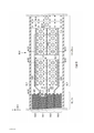
繼而,使用圖3及圖4對記憶胞陣列11之平面構成進行說明。圖3係1個區塊BLK中之串單元SU0~SU3之俯視圖。再者,於圖3之例中省略了層間絕緣膜。圖4係選擇閘極線SGDa~SGDd之各層之俯視圖。
Next, the planar configuration of the
如圖3所示,於本實施形態中,於與半導體基板垂直之Z方向上,自下層起積層有選擇閘極線SGS、字元線WL0~WL7及選擇閘極線SGDa~SGDd。串單元SU0~SU3係於與半導體基板平行且與Z方向交叉之Y方向上相鄰地設置。更具體而言,選擇閘極線SGDa~SGDd藉由狹縫SHE,而就各串單元SU被分離。再者,狹縫SHE未將設置於選擇閘極線SGD下方之字元線WL及選擇閘極線SGS分離。即,於選擇閘極線SGD之下方,共有串單元SU0~SU3之字元線WL及選擇閘極線SGS。並且,於串單元SU0及SU3之朝向Y方向之側面形成有狹縫SLT。狹縫SLT係以將選擇閘極線SGD、字元線WL及選擇閘極線SGS就各區塊BLK分離之方式設置。 As shown in FIG. 3, in this embodiment, in the Z direction perpendicular to the semiconductor substrate, select gate lines SGS, word lines WL0 to WL7, and select gate lines SGDa to SGDd are stacked from the lower layer. The string units SU0 to SU3 are adjacently arranged in the Y direction parallel to the semiconductor substrate and crossing the Z direction. More specifically, the selected gate lines SGDa to SGDd are separated for each string unit SU by the slit SHE. Furthermore, the slit SHE does not separate the word line WL and the select gate line SGS disposed under the select gate line SGD. That is, under the selection gate line SGD, there are a total of the word lines WL of the string units SU0~SU3 and the selection gate line SGS. In addition, slits SLT are formed on the side surfaces of the string units SU0 and SU3 facing the Y direction. The slit SLT is arranged in such a way that the selection gate line SGD, the word line WL, and the selection gate line SGS are separated for each block BLK.
各區塊BLK包含胞元部及階梯連接部。 Each block BLK includes a cell part and a step connection part.
於胞元部形成有與NAND串NS對應之複數個記憶體柱MP。關於記憶體柱MP之構造之詳細內容,將於下文進行敍述。於圖3之例中,記憶體柱MP係以朝向與半導體基板平行且與Y方向交叉之X方向成為16排(行)鋸齒配置之方式排列。並且,以記憶體柱MP於每個串單元SU成為4排鋸齒配置之方式,藉由沿X方向延伸之3個狹縫SHE將選擇閘極線 SGD就各串單元SU分離。再者,記憶體柱MP之排列可任意設定。例如,可朝向X方向排列成8排鋸齒配置,亦可排列成20排鋸齒配置,亦可為16個記憶體柱沿著Y方向排列成一行。 A plurality of memory pillars MP corresponding to the NAND string NS are formed in the cell part. The detailed content of the structure of the memory pillar MP will be described below. In the example of FIG. 3, the memory pillars MP are arranged in a zigzag arrangement of 16 rows (rows) toward the X direction parallel to the semiconductor substrate and crossing the Y direction. In addition, the memory pillar MP is arranged in 4 rows of zigzags in each string unit SU, and the gate line is selected by the 3 slits SHE extending in the X direction SGD separates each string unit SU. Furthermore, the arrangement of the memory column MP can be set arbitrarily. For example, it can be arranged in a zigzag arrangement of 8 rows toward the X direction, can also be arranged in a zigzag arrangement of 20 rows, or 16 memory columns can be arranged in a row along the Y direction.
複數個記憶體柱MP分別通過選擇閘極線SGD、字元線WL及選擇閘極線SGS,並沿Z方向延伸。各串單元SU之1個記憶體柱MP之上端例如藉由沿Y方向延伸之位元線BL(未圖示)而共通地連接。 The plurality of memory pillars MP respectively pass through the select gate line SGD, the word line WL, and the select gate line SGS, and extend along the Z direction. The upper end of one memory pillar MP of each string unit SU is commonly connected by, for example, a bit line BL (not shown) extending in the Y direction.
於階梯連接部形成有與選擇閘極線SGD及SGS以及字元線WL連接之複數個接觸插塞CC。選擇閘極線SGD及SGS以及字元線WL之各者經由接觸插塞CC而連接於列解碼器12。
A plurality of contact plugs CC connected to the selection gate lines SGD and SGS and the word line WL are formed in the step connection portion. Each of the select gate lines SGD and SGS and the word line WL is connected to the
於階梯連接部,與選擇閘極線SGD及SGS以及字元線WL對應之複數個配線層朝向X方向呈階梯狀被引出。並且,於各配線層之端部設置有與接觸插塞CC之連接部。以下,將連接部表述為「平台」。 At the step connection portion, a plurality of wiring layers corresponding to the selection gate lines SGD and SGS and the word line WL are drawn out stepwise in the X direction. In addition, a connection part with the contact plug CC is provided at the end of each wiring layer. Hereinafter, the connection part is expressed as "platform".
於本實施形態中,沿著X方向配置有與2個串單元SU之選擇閘極線SGD對應之複數個平台。即,與4個串單元SU之選擇閘極線SGD對應之複數個平台沿著X方向排列成2行。再者,與4個串單元SU之選擇閘極線SGD對應之複數個平台亦可沿著X方向排列成1行。 In this embodiment, a plurality of platforms corresponding to the selection gate lines SGD of the two string units SU are arranged along the X direction. That is, a plurality of lands corresponding to the selection gate lines SGD of the 4 string units SU are arranged in 2 rows along the X direction. Furthermore, a plurality of platforms corresponding to the selection gate lines SGD of the 4 string units SU can also be arranged in a row along the X direction.
更具體而言,於自胞元部朝向階梯連接部之X方向上,與串單元SU1之選擇閘極線SGD1d~SGD1a對應之複數個平台和與串單元SU0之選擇閘極線SGD0a~SGD0d對應之複數個平台排列成一行。 More specifically, in the X direction from the cell part to the step connection part, a plurality of platforms corresponding to the selection gate lines SGD1d~SGD1a of the string unit SU1 and corresponding to the selection gate lines SGD0a~SGD0d of the string unit SU0 The plural platforms are arranged in a row.
將胞元部中之串單元SU1之Y方向之長度設為L1,將串單元SU1之平台之Y方向之長度設為L2。於是,將串單元SU0之選擇閘極線SGD與串單元SU1之選擇閘極線SGD分離之狹縫SHE具有以長度L2長於長度L1之方式於XY平面內向串單元SU0側彎折之形狀(曲柄形狀)。將串 單元SU0之選擇閘極線SGD與串單元SU1之選擇閘極線SGD分離之狹縫SHE於向串單元SU0側彎折之部分,沿與半導體基板平行且與X方向及Y方向交叉之方向(相對於X方向及Y方向傾斜之方向)延伸。 The length in the Y direction of the string unit SU1 in the cell unit is set to L1, and the length in the Y direction of the platform of the string unit SU1 is set to L2. Therefore, the slit SHE separating the select gate line SGD of the string unit SU0 and the select gate line SGD of the string unit SU1 has a shape that is bent toward the string unit SU0 side in the XY plane such that the length L2 is longer than the length L1 (crank shape). Will string The slit SHE separating the select gate line SGD of the unit SU0 from the select gate line SGD of the string unit SU1 is at the part bent toward the string unit SU0 along the direction parallel to the semiconductor substrate and crossing the X direction and the Y direction ( It extends in a direction inclined with respect to the X direction and the Y direction.
同樣地,於自胞元部朝向階梯連接部之X方向上,與串單元SU2之選擇閘極線SGD2d~SGD2a對應之複數個平台和與串單元SU3之選擇閘極線SGD3a~SGD3d對應之複數個平台排列成一行。 Similarly, in the X direction from the cell part to the step connection part, the plural platforms corresponding to the selection gate lines SGD2d~SGD2a of the string unit SU2 and the plural numbers corresponding to the selection gate lines SGD3a~SGD3d of the string unit SU3 The platforms are arranged in a row.
將串單元SU2之選擇閘極線SGD與串單元SU3之選擇閘極線SGD分離之狹縫SHE係沿著X方向設置。並且,將串單元SU2之選擇閘極線SGD與串單元SU3之選擇閘極線SGD分離之狹縫SHE具有以串單元SU2之平台之Y方向之長度長於胞元部中之串單元SU2之Y方向之長度之方式於XY平面內向串單元SU3側彎折之曲柄形狀。將串單元SU2之選擇閘極線SGD與串單元SU3之選擇閘極線SGD分離之狹縫SHE於向串單元SU3側彎折之部分,沿與半導體基板平行且與X方向及Y方向交叉之方向(相對於X方向及Y方向傾斜之方向)延伸。 The slit SHE separating the select gate line SGD of the string unit SU2 and the select gate line SGD of the string unit SU3 is arranged along the X direction. Also, the slit SHE separating the select gate line SGD of the string unit SU2 from the select gate line SGD of the string unit SU3 has a length in the Y direction of the platform of the string unit SU2 that is longer than the Y of the string unit SU2 in the cell portion The length of the direction is in the shape of a crank bent toward the SU3 side of the string unit in the XY plane. The slit SHE separating the select gate line SGD of the string unit SU2 from the select gate line SGD of the string unit SU3 is along the part that is bent to the side of the string unit SU3, which is parallel to the semiconductor substrate and crosses the X and Y directions The direction (the direction inclined with respect to the X direction and the Y direction) extends.
再者,將串單元SU1之選擇閘極線SGD與串單元SU2之選擇閘極線SGD分離之狹縫SHE並未自胞元部至階梯連接部彎折,而是沿著X方向呈直線狀延伸。又,與字元線WL7~WL0對應之平台例如於自胞元部朝向階梯連接部之X方向上排列成一行。 Furthermore, the slit SHE separating the select gate line SGD of the string unit SU1 and the select gate line SGD of the string unit SU2 is not bent from the cell part to the step connection part, but is straight along the X direction extend. In addition, the platforms corresponding to the character lines WL7 to WL0 are arranged in a row, for example, in the X direction from the cell portion to the step connection portion.
與平台之排列同樣地,與4個串單元SU0~SU3之選擇閘極線SGDa~SGDd分別對應之複數個接觸插塞CC沿著X方向排列成2行。 Similar to the arrangement of the platform, the plurality of contact plugs CC corresponding to the selection gate lines SGDa~SGDd of the 4 string units SU0~SU3 are arranged in 2 rows along the X direction.
又,於階梯連接部設置有複數個虛設柱HR,該等複數個虛設柱HR貫通與選擇閘極線SGD及SGS以及字元線WL對應之複數個配線層。更具體而言,例如,設置於與選擇閘極線SGDd對應之平台上之虛設 柱HR貫通選擇閘極線SGDa~SGDd及SGS以及字元線WL0~WL7。例如,設置於與選擇閘極線SGDa對應之平台上之虛設柱HR貫通選擇閘極線SGDa及SGS以及字元線WL0~WL7。又,例如,設置於與字元線WL7對應之平台上之虛設柱HR貫通選擇閘極線SGS以及字元線WL0~WL7。再者,虛設柱HR之配置可任意。虛設柱HR不與配線層電性連接。作為選擇閘極線SGD及SGS以及字元線WL之形成方法,例如有在犧牲層形成相當於各配線層之構造後將犧牲層替換成導電材料而形成配線層之方法(以下,稱為「替換」)。於替換中,將犧牲層去除而形成空隙後,藉由導電材料填埋該空隙。因此,虛設柱HR係作為支撐具有空隙之層間絕緣膜之柱發揮功能。 In addition, a plurality of dummy pillars HR are provided at the step connection portion, and the plurality of dummy pillars HR penetrate through a plurality of wiring layers corresponding to the selection gate lines SGD and SGS and the word line WL. More specifically, for example, a dummy set on the platform corresponding to the selection gate line SGDd The column HR penetrates the selection gate lines SGDa~SGDd and SGS and the word lines WL0~WL7. For example, the dummy column HR provided on the platform corresponding to the selection gate line SGDa penetrates the selection gate lines SGDa and SGS and the word lines WL0 to WL7. Also, for example, the dummy pillar HR provided on the platform corresponding to the word line WL7 penetrates the selection gate line SGS and the word lines WL0 to WL7. Furthermore, the configuration of the dummy column HR can be arbitrary. The dummy post HR is not electrically connected to the wiring layer. As a method of forming selective gate lines SGD and SGS and word line WL, for example, there is a method of forming a wiring layer by replacing the sacrificial layer with a conductive material after forming a structure equivalent to each wiring layer in the sacrificial layer (hereinafter referred to as " replace"). In the replacement, after the sacrificial layer is removed to form a void, the void is filled with a conductive material. Therefore, the dummy post HR functions as a post supporting the interlayer insulating film with voids.
繼而,對選擇閘極線SGDa~SGDd之各層之平面構成之詳細內容進行說明。 Next, the detailed content of the planar configuration of each layer of the selected gate lines SGDa to SGDd will be described.
如圖4所示,首先,若著眼於選擇閘極線SGDd,則選擇閘極線SGD0d~SGD3d藉由複數個狹縫SHE而相互分離。選擇閘極線SGD1d及SGD2d之平台係沿著Y方向配置。同樣地,選擇閘極線SGD0d及SGD3d之平台係沿著Y方向配置。又,選擇閘極線SGD1d及SGD0d之平台係沿著X方向配置。同樣地,選擇閘極線SGD2d及SGD3d之平台係沿著X方向配置。於各平台上連接有接觸插塞CC(圖4之參照符號“CC連接位置”)。 As shown in FIG. 4, first, if focusing on the selection gate line SGDd, the selection gate lines SGD0d to SGD3d are separated from each other by a plurality of slits SHE. The platforms for selecting gate lines SGD1d and SGD2d are arranged along the Y direction. Similarly, the platforms of the selection gate lines SGD0d and SGD3d are arranged along the Y direction. In addition, the plateaus for selecting the gate lines SGD1d and SGD0d are arranged along the X direction. Similarly, the platforms for selecting the gate lines SGD2d and SGD3d are arranged along the X direction. A contact plug CC is connected to each platform (reference symbol "CC connection position" in Figure 4).
選擇閘極線SGD0d及SGD3d於階梯連接部分別包含沿X方向延伸之引出電極HE。引出電極HE係作為用以向遠離胞元部之X方向(圖4之紙面右側)引出平台之電極發揮功能。再者,例如,於串單元SU0中,引出電極HE之Y方向上之長度短於胞元部中之選擇閘極線SGD0d之Y方向 之長度。選擇閘極線SGD0d及SGD3d之平台配置於較選擇閘極線SGD1d及SGD2d之平台更遠離胞元部之位置。 The selection gate lines SGD0d and SGD3d respectively include lead electrodes HE extending in the X direction at the step connection portion. The extraction electrode HE functions as an electrode for extracting the platform in the X direction away from the cell part (right side of the paper in FIG. 4). Furthermore, for example, in the string unit SU0, the length of the lead electrode HE in the Y direction is shorter than the Y direction of the selection gate line SGD0d in the cell portion The length. The platforms for selecting gate lines SGD0d and SGD3d are arranged at positions farther from the cell part than the platforms for selecting gate lines SGD1d and SGD2d.
繼而,若著眼於選擇閘極線SGDc,則選擇閘極線SGD0c~SGD3c藉由狹縫SHE而相互分離。選擇閘極線SGD1c及SGD2c之平台係沿著Y方向配置。同樣地,選擇閘極線SGD0c及SGD3c之平台係沿著Y方向配置。又,選擇閘極線SGD1c及SGD0c之平台係沿著X方向配置。同樣地,選擇閘極線SGD2c及SGD3c之平台係沿著X方向配置。 Then, if focusing on the selection gate line SGDc, the selection gate lines SGD0c to SGD3c are separated from each other by the slit SHE. The platforms for selecting gate lines SGD1c and SGD2c are arranged along the Y direction. Similarly, the platforms of the selection gate lines SGD0c and SGD3c are arranged along the Y direction. In addition, the terraces for selecting the gate lines SGD1c and SGD0c are arranged along the X direction. Similarly, the platforms for selecting gate lines SGD2c and SGD3c are arranged along the X direction.
選擇閘極線SGD1c及SGD2c之平台係以與設置於上方之選擇閘極線SGD1d及SGD2d之平台成為階梯狀之方式配置於較選擇閘極線SGD1d及SGD2d之平台更遠離胞元部之位置。選擇閘極線SGD0c及SGD3c分別包含引出電極HE。選擇閘極線SGD0c及SGD3c之平台配置於較選擇閘極線SGD1c及SGD2c之平台更遠離胞元部之位置。又,選擇閘極線SGD0c及SGD3c之平台係以與設置於上方之選擇閘極線SGD0d及SGD3d之平台成為階梯狀之方式配置於較選擇閘極線SGD0d及SGD3d之平台更靠近胞元部之位置。 The platforms of the selection gate lines SGD1c and SGD2c are arranged in a stepped manner with the platforms of the upper selection gate lines SGD1d and SGD2d at positions farther from the cell than the platforms of the selection gate lines SGD1d and SGD2d. The selection gate lines SGD0c and SGD3c respectively include lead electrodes HE. The platforms of the selection gate lines SGD0c and SGD3c are arranged at positions farther from the cell part than the platforms of the selection gate lines SGD1c and SGD2c. In addition, the platforms for the selection gate lines SGD0c and SGD3c are arranged in a stepped manner with the platforms for the selection gate lines SGD0d and SGD3d arranged above, and are arranged closer to the cell part than the platforms for the selection gate lines SGD0d and SGD3d position.
繼而,若著眼於選擇閘極線SGDb,則選擇閘極線SGD0b~SGD3b藉由狹縫SHE而相互分離。選擇閘極線SGD1b及SGD2b之平台係沿著Y方向配置。同樣地,選擇閘極線SGD0b及SGD3b之平台係沿著Y方向配置。又,選擇閘極線SGD1b及SGD0b之平台係沿著X方向配置。同樣地,選擇閘極線SGD2b及SGD3b之平台係沿著X方向配置。 Then, if focusing on the selection gate line SGDb, the selection gate lines SGD0b to SGD3b are separated from each other by the slit SHE. The platforms for selecting gate lines SGD1b and SGD2b are arranged along the Y direction. Similarly, the platforms of the selection gate lines SGD0b and SGD3b are arranged along the Y direction. In addition, the platforms for selecting the gate lines SGD1b and SGD0b are arranged along the X direction. Similarly, the platforms for selecting gate lines SGD2b and SGD3b are arranged along the X direction.
選擇閘極線SGD1b及SGD2b之平台係以與設置於上方之選擇閘極線SGD1c及SGD2c之平台成為階梯狀之方式配置於較選擇閘極線SGD1c及SGD2c之平台更遠離胞元部之位置。選擇閘極線SGD0b及 SGD3b分別包含引出電極HE。選擇閘極線SGD0b及SGD3b之平台配置於較選擇閘極線SGD1b及SGD2b之平台更遠離胞元部之位置。又,選擇閘極線SGD0b及SGD3b之平台係以與設置於上方之選擇閘極線SGD0c及SGD3c之平台成為階梯狀之方式配置於較選擇閘極線SGD0c及SGD3c之平台更靠近胞元部之位置。 The platforms of the selection gate lines SGD1b and SGD2b are arranged in a stepped manner with the platforms of the upper selection gate lines SGD1c and SGD2c at a position farther from the cell than the platforms of the selection gate lines SGD1c and SGD2c. Select the gate line SGD0b and SGD3b respectively contains the lead electrode HE. The platforms of the selection gate lines SGD0b and SGD3b are arranged at positions farther from the cell part than the platforms of the selection gate lines SGD1b and SGD2b. In addition, the platforms for the selection gate lines SGD0b and SGD3b are arranged in a stepped manner with the platforms for the selection gate lines SGD0c and SGD3c arranged above, and are arranged closer to the cell part than the platforms for the selection gate lines SGD0c and SGD3c. position.
繼而,若著眼於選擇閘極線SGDa,則選擇閘極線SGD0a~SGD3a藉由狹縫SHE而相互分離。選擇閘極線SGD1a及SGD2a之平台係沿著Y方向配置。同樣地,選擇閘極線SGD0a及SGD3a之平台係沿著Y方向配置。又,選擇閘極線SGD1a及SGD0a之平台係沿著X方向配置。同樣地,選擇閘極線SGD2a及SGD3a之平台係沿著X方向配置。 Then, when focusing on the selection gate line SGDa, the selection gate lines SGD0a to SGD3a are separated from each other by the slit SHE. The platforms for selecting gate lines SGD1a and SGD2a are arranged along the Y direction. Similarly, the platforms of the selection gate lines SGD0a and SGD3a are arranged along the Y direction. In addition, the platforms for selecting gate lines SGD1a and SGD0a are arranged along the X direction. Similarly, the platforms for selecting gate lines SGD2a and SGD3a are arranged along the X direction.
選擇閘極線SGD1a及SGD2a之平台係以與設置於上方之選擇閘極線SGD1b及SGD2b之平台成為階梯狀之方式配置於較選擇閘極線SGD1b及SGD2b之平台更遠離胞元部之位置。選擇閘極線SGD0a及SGD3a分別包含引出電極HE。選擇閘極線SGD0a及SGD3a之平台配置於較選擇閘極線SGD1a及SGD2a之平台更遠離胞元部之位置。又,選擇閘極線SGD0a及SGD3a之平台係以與設置於上方之選擇閘極線SGD0b及SGD3b之平台成為階梯狀之方式配置於較選擇閘極線SGD0b及SGD3b之平台更靠近胞元部之位置。 The platforms of the selection gate lines SGD1a and SGD2a are arranged in a stepped manner with the platforms of the upper selection gate lines SGD1b and SGD2b at a position farther from the cell than the platforms of the selection gate lines SGD1b and SGD2b. The selection gate lines SGD0a and SGD3a respectively include lead electrodes HE. The platforms of the selection gate lines SGD0a and SGD3a are arranged at positions farther from the cell portion than the platforms of the selection gate lines SGD1a and SGD2a. In addition, the platforms of the selection gate lines SGD0a and SGD3a are arranged in a stepped manner with the platforms of the selection gate lines SGD0b and SGD3b arranged above, and are arranged closer to the cell part than the platforms of the selection gate lines SGD0b and SGD3b. position.
1.1.4記憶胞陣列之剖面構成 1.1.4 Cross-sectional structure of memory cell array
繼而,使用圖5~圖8對記憶胞陣列11之剖面構成進行說明。圖5係沿著圖3之A1-A2線之剖視圖。圖6係沿著圖3之B1-B2線之剖視圖。圖7係沿著圖3之C1-C2線之剖視圖。圖8係沿著圖3之D1-D2線之剖視圖。
Next, the cross-sectional structure of the
如圖5所示,於半導體基板30上形成有絕緣層31。絕緣層
31係使用例如氧化矽膜(SiO2)。再者,亦可於形成有絕緣層31之區域、即半導體基板30與配線層32之間設置有列解碼器12或感測放大器13等之電路。
As shown in FIG. 5, an insulating
於絕緣層31上形成有作為源極線SL發揮功能之配線層32。配線層32係由導電材料構成,例如使用n型半導體、p型半導體或金屬材料。
A
於配線層32上交替地積層有14層絕緣層33及自下層起作為選擇閘極線SGS、字元線WL0~WL7及選擇閘極線SGDa~SGDd發揮功能之13層配線層34。
On the
絕緣層33例如使用SiO2。配線層34係由導電材料構成,例如使用n型半導體、p型半導體或金屬材料。以下,對使用氮化鈦(TiN)/鎢(W)之積層構造作為配線層34之情形進行說明。TiN例如於藉由CVD(chemical vapor deposition,化學氣相沈積)使W成膜時,具有作為用以防止W與SiO2之反應之障壁層或者用以提高W之密接性之密接層之功能。
For the insulating
形成有貫通14層絕緣層33與13層配線層34且底面到達配線層32之記憶體柱MP。1個記憶體柱MP與1個NAND串NS對應。記憶體柱MP包含阻擋絕緣膜35、電荷累積層36、隧道絕緣膜37、半導體層38、核心層39及頂蓋層40。
A memory pillar MP is formed that penetrates the 14-
更具體而言,以貫通絕緣層33及配線層34且底面到達配線層32之方式形成有與記憶體柱MP對應之孔。於孔之側面依序積層有阻擋絕緣膜35、電荷累積層36及隧道絕緣膜37。並且,以側面與隧道絕緣膜37相接且底面與配線層32相接之方式形成有半導體層38。半導體層38係
供形成記憶胞電晶體MC以及選擇電晶體ST1及ST2之通道之區域。因此,半導體層38係作為將選擇電晶體ST2、記憶胞電晶體MC0~MC7及選擇電晶體ST1a~ST1d之電流路徑連接之信號線發揮功能。於半導體層38內設置有核心層39。並且,於半導體層38及核心層39上,形成有側面與隧道絕緣膜37相接之頂蓋層40。於頂蓋層40上形成有未圖示之接觸插塞。於接觸插塞上形成有作為位元線BL發揮功能之配線層。
More specifically, a hole corresponding to the memory pillar MP is formed so as to penetrate through the insulating
阻擋絕緣膜35、隧道絕緣膜37及核心層39例如使用SiO2。電荷累積層36例如使用氮化矽膜(SiN)。半導體層38及頂蓋層40例如使用多晶矽。
For the
以將作為選擇閘極線SGDa~SGDd發揮功能之4層配線層34就各串單元SU分離之方式形成狹縫SHE。狹縫SHE內由絕緣層41填埋。又,以將13層配線層34就各區塊BLK分離之方式形成沿X方向延伸之狹縫SLT。狹縫SLT內由絕緣層42填埋。絕緣層41及42例如使用SiO2。
The slit SHE is formed so that the four-
由記憶體柱MP及分別作為字元線WL0~WL7發揮功能之8層配線層34分別構成記憶胞電晶體MC0~MC7。同樣地,由記憶體柱MP及分別作為選擇閘極線SGDa~SGDd及SGS發揮功能之5層配線層34分別構成選擇電晶體ST1a~ST1d及ST2。
The memory pillar MP and the 8-
繼而,對串單元SU1之選擇閘極線SGD1a之平台與串單元SU2之選擇閘極線SGD2a之平台進行說明。 Then, the platform of the selection gate line SGD1a of the string unit SU1 and the platform of the selection gate line SGD2a of the string unit SU2 will be described.
如圖6所示,於選擇閘極線SGD1a之平台之上方並未形成選擇閘極線SGD1b~1d。同樣地,於選擇閘極線SGD2a之平台之上方並未形成選擇閘極線SGD2b~2d。選擇閘極線SGD1a及SGD2a之平台藉由絕緣層41(狹縫SHE)而相互分離,又,藉由絕緣層41(狹縫SHE)而與選擇
閘極線SGD0a~SGD0d及SGD3a~SGD3d之引出電極HE分離。於選擇閘極線SGD1a及SGD2a之平台上分別形成有作為接觸插塞CC發揮功能之導電層43。導電層43係由導電材料構成,亦可使用例如鎢(W)或氮化鈦(TiN)等金屬材料。
As shown in FIG. 6, the selection gate lines SGD1b~1d are not formed above the platform of the selection gate line SGD1a. Similarly, the selection gate lines SGD2b~2d are not formed above the platform of the selection gate line SGD2a. The platforms of the selection gate lines SGD1a and SGD2a are separated from each other by the insulating layer 41 (slit SHE), and furthermore, the insulating layer 41 (slit SHE) is connected to the selection
The lead electrodes HE of the gate lines SGD0a~SGD0d and SGD3a~SGD3d are separated.
繼而,對串單元SU0之選擇閘極線SGD0a之平台與串單元SU3之選擇閘極線SGD3a之平台進行說明。 Then, the platform of the selection gate line SGD0a of the string unit SU0 and the platform of the selection gate line SGD3a of the string unit SU3 will be described.
如圖7所示,於選擇閘極線SGD0a之平台之上方並未形成選擇閘極線SGD0b~0d。同樣地,於選擇閘極線SGD3a之平台之上方並未形成選擇閘極線SGD3b~3d。選擇閘極線SGD0a及SGD3a之平台藉由絕緣層41(狹縫SHE)而相互分離。並且,於選擇閘極線SGD0a及SGD3a之平台上形成有作為接觸插塞CC發揮功能之導電層43。
As shown in FIG. 7, the selection gate lines SGD0b~0d are not formed above the platform of the selection gate line SGD0a. Similarly, the selection gate lines SGD3b~3d are not formed above the platform of the selection gate line SGD3a. The terraces of the selection gate lines SGD0a and SGD3a are separated from each other by the insulating layer 41 (slit SHE). In addition, a
繼而,對X方向上之階梯連接部之剖面構成之一部分進行說明。 Next, a part of the cross-sectional configuration of the stepped connection portion in the X direction will be described.
如圖8所示,自胞元部沿著X方向於階梯連接部配置有串單元SU1之選擇閘極線SGD1d、SGD1c、SGD1b及SGD1a之平台、以及串單元SU0之選擇閘極線SGD0a、SGD0b、SGD0c及SGD0d之平台。於各平台上形成有作為接觸插塞CC發揮功能之導電層43。
As shown in FIG. 8, from the cell part along the X direction at the step connection part, the platform of the selection gate lines SGD1d, SGD1c, SGD1b, and SGD1a of the string unit SU1, and the selection gate lines SGD0a, SGD0b of the string unit SU0 are arranged at the step connection part. , SGD0c and SGD0d platforms. A
1.2階梯連接部中之選擇閘極線SGD之平台形成方法 1.2 The platform formation method of the selected gate line SGD in the step connection part
繼而,使用圖9~圖11對階梯連接部中之選擇閘極線SGD之平台形成方法進行說明。圖9~圖11示出了沿著圖3中之D1-D2線之剖面。於本實施形態中,對藉由替換而形成配線層34之情形進行說明。再者,以下,為了簡化說明,對與選擇閘極線SGD對應之犧牲層之加工進行說明,關於與字元線WL及選擇閘極線SGS對應之犧牲層之加工則省略說明。
Next, the method for forming the platform of the selective gate line SGD in the step connection part will be described using FIGS. 9-11. Figures 9-11 show the cross-sections along the line D1-D2 in Figure 3. In this embodiment, a case where the
如圖9所示,於配線層32上交替地積層14層絕緣層33及分別與13層配線層34對應之13層犧牲層44。犧牲層例如使用SiN。再者,犧牲層並不限定於SiN。犧牲層44例如只要為可與絕緣層33充分地獲得濕式蝕刻之選擇比之材料即可。
As shown in FIG. 9, on the
繼而,使用奈米壓印-微影(nanoimprint lithography)技術於最上層之絕緣層33上形成模板轉印層45。模板轉印層45例如使用紫外線硬化性樹脂。模板轉印層45係作為對絕緣層33及犧牲層44進行加工時之遮罩圖案發揮功能。模板轉印層45係為了將與選擇閘極線SGDa~SGDd對應之4層犧牲層44加工成4段階梯狀而具有4段階梯形狀。更具體而言,自模板轉印層45之下側起第1段與選擇閘極線SGDa對應。藉此,於對4層犧牲層44進行加工時,自上層起3層犧牲層44被加工。自下側起第2段與選擇閘極線SGDb對應。藉此,於對4層犧牲層44進行加工時,自上層起2層犧牲層44被加工。自下側起第3段與選擇閘極線SGDc對應。藉此,於對4層犧牲層44進行加工時,最上層之犧牲層44被加工。最上段與選擇閘極線SGDd對應。藉此,於對4層犧牲層44進行加工時,防止最上層之犧牲層44被加工。
Then, a nanoimprint lithography technique is used to form a
如圖10所示,繼而,自上層起對4層犧牲層44進行加工。此時,藉由模板轉印層45,而於階梯連接部將4層犧牲層44加工成與選擇閘極線SGDa~SGDd對應之4段階梯狀。
As shown in FIG. 10, four
再者,於圖9及圖10之例中,對使用奈米壓印-微影技術將與選擇閘極線SGDa~SGDd對應之4層犧牲層44加工成4段階梯形狀之情形進行了說明,但犧牲層44之加工方法並不限定於此。例如,亦可使用光微影技術並利用抗蝕劑形成遮罩圖案,對4層犧牲層44進行加工。於該情
形時,可與選擇閘極線SGDa~SGDd對應地反覆進行4次曝光與加工,亦可藉由利用細化處理改變遮罩圖案之尺寸而將4層犧牲層44加工成4段階梯形狀。
Furthermore, in the examples of FIGS. 9 and 10, the case where the 4-layer
如圖11所示,於與字元線WL及選擇閘極線SGS對應之犧牲層44亦加工成階梯狀後,於犧牲層44上形成絕緣層33,例如藉由CMP(chemical mechanical polishing,化學機械拋光)等使表面平坦化。然後,藉由替換將13層犧牲層44替換成配線層34。更具體而言,於形成虛設柱HR後,以13層犧牲層44於側面露出之方式形成狹縫SLT之槽圖案。繼而,藉由濕式蝕刻自狹縫SLT側面將犧牲層44去除而形成空隙。繼而,例如使用TiN及W將空隙內填埋後,將狹縫SLT內及最上層之絕緣層33上之TiN及W去除。繼而,藉由絕緣層42填埋狹縫SLT。
As shown in FIG. 11, after the
於替換後,如圖8所示,形成導電層43。
After the replacement, as shown in FIG. 8, a
1.3本實施形態之效果 1.3 Effects of this embodiment
若為本實施形態之構成,則能夠提高可靠性。對本效果進行詳細敍述。 With the configuration of this embodiment, reliability can be improved. This effect is described in detail.
例如,於在2個狹縫SLT間配置1個區塊BLK、即4個串單元SU之情形時,4個串單元SU之選擇閘極線SGD藉由狹縫SHE而相互分離。例如,於在Y方向上相鄰之4個串單元SU中,存在將4個串單元SU之選擇閘極線SGD之平台對照串單元SU之配置而於X方向上配置成4行之情形。於該情形時,若Y方向上之狹縫SLT間隔縮小,則各選擇閘極線SGD之平台之Y方向上之長度變短。若平台之長度變短,則產生因製造偏差而引起之平台(選擇閘極線SGD)與接觸插塞CC之位置偏移所導致之連接不良、或因接觸插塞CC與於Y方向上相鄰之非連接之選擇閘極線SGD之距 離變短所導致之耐受電壓不良之可能性增高。又,無法於平台上充分地確保虛設柱HR之配置空間。 For example, when one block BLK is arranged between two slits SLT, that is, four string units SU, the selection gate lines SGD of the four string units SU are separated from each other by the slit SHE. For example, among the 4 string units SU adjacent to each other in the Y direction, there is a case in which the platforms of the select gate lines SGD of the 4 string units SU are arranged in 4 rows in the X direction against the arrangement of the string units SU. In this case, if the gap between the slits SLT in the Y direction is reduced, the length in the Y direction of the platform of each selected gate line SGD becomes shorter. If the length of the platform becomes shorter, poor connection caused by the positional deviation of the platform (selection gate line SGD) and the contact plug CC caused by the manufacturing deviation, or the contact plug CC is opposite to the Y direction Distance between adjacent non-connected select gate lines SGD The possibility of poor withstand voltage caused by the short circuit becomes higher. In addition, it is impossible to sufficiently ensure the arrangement space of the dummy column HR on the platform.
相對於此,若為本實施形態之構成,則於在Y方向上相鄰之4個串單元SU中,可將4個串單元SU之選擇閘極線SGD之平台於X方向上配置成2行。即,可將於Y方向上相鄰之2個選擇閘極線SGD之平台沿X方向配置成1行。藉此,即便於Y方向上之狹縫SLT間隔縮小之情形時,亦可藉由調整引出電極HE之Y方向上之長度來抑制各選擇閘極線SGD之平台之Y方向上之長度變短。因此,可抑制選擇閘極線SGD與接觸插塞CC之連接不良及耐受電壓不良,從而能夠提高半導體記憶裝置之可靠性。 On the other hand, in the configuration of this embodiment, among the 4 string units SU adjacent in the Y direction, the platforms of the selection gate lines SGD of the 4 string units SU can be arranged in the X direction to 2 Row. That is, the plateaus of the two adjacent selection gate lines SGD in the Y direction can be arranged in one row along the X direction. As a result, even when the gap between the slits SLT in the Y direction is reduced, the length in the Y direction of each selection gate line SGD can be suppressed by adjusting the length of the lead electrode HE in the Y direction. . Therefore, poor connection between the selection gate line SGD and the contact plug CC and poor withstand voltage can be suppressed, and the reliability of the semiconductor memory device can be improved.
進而,可確保選擇閘極線SGD之平台上之虛設柱HR之配置空間,故而於藉由替換形成配線層時,可抑制形成不良。 Furthermore, the arrangement space of the dummy post HR on the platform for selecting the gate line SGD can be ensured, so when the wiring layer is formed by replacement, the formation failure can be suppressed.
2.第2實施形態 2. The second embodiment
繼而,對第2實施形態進行說明。於第2實施形態中,對與第1實施形態不同之選擇閘極線SGD之平台之配置進行說明。以下,以與第1實施形態不同之方面為中心進行說明。 Next, the second embodiment will be described. In the second embodiment, the arrangement of the platform for selecting the gate line SGD which is different from the first embodiment will be described. Hereinafter, the description will be focused on the differences from the first embodiment.
2.1記憶胞陣列之平面構成 2.1 Plane composition of memory cell array
使用圖12及圖13對本實施形態之記憶胞陣列11之平面構成進行說明。圖12係1個區塊BLK中之串單元SU0~SU3之俯視圖。再者,於圖12之例中省略了層間絕緣膜。圖13係選擇閘極線SGDa~SGDd之各層之俯視圖。
The planar configuration of the
如圖12所示,於本實施形態中,於自胞元部朝向階梯連接部之X方向上,與串單元SU1之選擇閘極線SGD1d~SGD1a對應之複數個平台和與串單元SU0之選擇閘極線SGD0d~SGD0a對應之複數個平台排列 成一行。同樣地,於自胞元部朝向階梯連接部之X方向上,與串單元SU2之選擇閘極線SGD2d~SGD2a對應之複數個平台和與串單元SU3之選擇閘極線SGD3d~SGD3a對應之複數個平台排列成一行。其他構成與第1實施形態之圖3相同。 As shown in FIG. 12, in this embodiment, in the X direction from the cell part to the step connection part, the multiple platforms corresponding to the selection gate lines SGD1d~SGD1a of the string unit SU1 and the selection of the string unit SU0 Arrangement of multiple platforms corresponding to gate lines SGD0d~SGD0a In a row. Similarly, in the X direction from the cell part to the step connection part, the plural platforms corresponding to the selection gate lines SGD2d~SGD2a of the string unit SU2 and the plural numbers corresponding to the selection gate lines SGD3d~SGD3a of the string unit SU3 The platforms are arranged in a row. The other structure is the same as that of Fig. 3 of the first embodiment.
繼而,對選擇閘極線SGDa~SGDd之各層之平面構成之詳細內容進行說明。 Next, the detailed content of the planar configuration of each layer of the selected gate lines SGDa to SGDd will be described.
如圖13所示,首先,若著眼於選擇閘極線SGDd,則選擇閘極線SGD0d及SGD3d之平台配置於較選擇閘極線SGD1d及SGD2d之平台更遠離胞元部之位置。 As shown in FIG. 13, first, if the focus is on selecting the gate line SGDd, the platforms of the selected gate lines SGD0d and SGD3d are arranged at a position farther from the cell portion than the platforms of the selected gate lines SGD1d and SGD2d.
繼而,若著眼於選擇閘極線SGDc,則選擇閘極線SGD1c及SGD2c之平台以與設置於上方之選擇閘極線SGD1d及SGD2d之平台成為階梯狀之方式配置於較選擇閘極線SGD1d及SGD2d之平台更遠離胞元部之位置。選擇閘極線SGD0c及SGD3c之平台配置於較選擇閘極線SGD1c及SGD2c之平台更遠離胞元部之配置。又,選擇閘極線SGD0c及SGD3c之平台以與設置於上方之選擇閘極線SGD0d及SGD3d之平台成為階梯狀之方式配置於較選擇閘極線SGD0d及SGD3d之平台更遠離胞元部之位置。 Then, if the focus is on the selection gate line SGDc, the platforms of the selection gate lines SGD1c and SGD2c are arranged in a stepwise manner with the platforms of the selection gate lines SGD1d and SGD2d arranged above the selection gate lines SGD1d and The platform of SGD2d is farther away from the cell part. The platform for selecting the gate lines SGD0c and SGD3c is arranged at a location farther from the cell part than the platform for selecting the gate lines SGD1c and SGD2c. In addition, the platforms of the selected gate lines SGD0c and SGD3c are arranged in a stepped manner with the platforms of the selected gate lines SGD0d and SGD3d arranged above, and are arranged at a position farther from the cell than the platforms of the selected gate lines SGD0d and SGD3d .
繼而,若著眼於選擇閘極線SGDb,則選擇閘極線SGD1b及SGD2b之平台以與設置於上方之選擇閘極線SGD1c及SGD2c之平台成為階梯狀之方式配置於較選擇閘極線SGD1c及SGD2c之平台更遠離胞元部之位置。選擇閘極線SGD0b及SGD3b之平台配置於較選擇閘極線SGD1b及SGD2b之平台更遠離胞元部之位置。又,選擇閘極線SGD0b及SGD3b之平台以與設置於上方之選擇閘極線SGD0c及SGD3c之平台成為 階梯狀之方式配置於較選擇閘極線SGD0c及SGD3c之平台更遠離胞元部之位置。 Then, if the focus is on the selected gate line SGDb, the platforms of the selected gate lines SGD1b and SGD2b are arranged in a stepwise manner with the platforms of the selected gate lines SGD1c and SGD2c arranged above the selected gate lines SGD1c and The platform of SGD2c is farther away from the cell part. The platforms of the selection gate lines SGD0b and SGD3b are arranged at positions farther from the cell part than the platforms of the selection gate lines SGD1b and SGD2b. In addition, the platform for selecting gate lines SGD0b and SGD3b becomes the platform for selecting gate lines SGD0c and SGD3c set above The stepwise arrangement is arranged at a position farther from the cell part than the platform of the selection gate lines SGD0c and SGD3c.
繼而,若著眼於選擇閘極線SGDa,則選擇閘極線SGD1a及SGD2a之平台以與設置於上方之選擇閘極線SGD1b及SGD2b之平台成為階梯狀之方式配置於較選擇閘極線SGD1b及SGD2b之平台更遠離胞元部之位置。選擇閘極線SGD0a及SGD3a之平台配置於較選擇閘極線SGD1a及SGD2a之平台更遠離胞元部之位置。又,選擇閘極線SGD0a及SGD3a之平台以與設置於上方之選擇閘極線SGD0b及SGD3b之平台成為階梯狀之方式配置於較選擇閘極線SGD0b及SGD3b之平台更遠離胞元部之位置。 Then, if focusing on the selection gate line SGDa, the platforms of the selection gate lines SGD1a and SGD2a are arranged in a stepwise manner with the platforms of the selection gate lines SGD1b and SGD2b set above the selection gate lines SGD1b and The platform of SGD2b is farther away from the cell part. The platforms of the selection gate lines SGD0a and SGD3a are arranged at positions farther from the cell portion than the platforms of the selection gate lines SGD1a and SGD2a. In addition, the platforms of the selected gate lines SGD0a and SGD3a are arranged in a stepped manner with the platforms of the selected gate lines SGD0b and SGD3b located above, and are arranged at a position farther from the cell than the platforms of the selected gate lines SGD0b and SGD3b .
2.2記憶胞陣列之剖面構成 2.2 Cross-sectional structure of memory cell array
繼而,使用圖14對記憶胞陣列11之剖面構成進行說明。圖14係沿著圖12之D1-D2線之剖視圖。
Next, the cross-sectional structure of the
如圖14所示,自胞元部沿著X方向於階梯連接部配置有串單元SU1之選擇閘極線SGD1d、SGD1c、SGD1b及SGD1a之平台、以及串單元SU0之選擇閘極線SGD0d、SGD0c、SGD0b及SGD0a之平台。於各平台上形成有導電層43。
As shown in FIG. 14, from the cell part along the X direction at the step connection part, there are platforms for the selection gate lines SGD1d, SGD1c, SGD1b, and SGD1a of the string unit SU1, and the selection gate lines SGD0d, SGD0c of the string unit SU0. , SGD0b and SGD0a platforms. A
2.3本實施形態之效果 2.3 Effects of this embodiment
若為本實施形態之構成,則可獲得與第1實施形態相同之效果。 With the configuration of this embodiment, the same effect as the first embodiment can be obtained.
3.變化例等 3. Examples of changes
上述實施形態之半導體記憶裝置包含:複數個第1配線層(WL),其等在第1方向(Z方向)上相互隔開地積層於基板(30)上;第2配線層(SGD0a),其與複數個第1配線層(WL)於第1方向(Z方向)上隔開地積層於 複數個第1配線層(WL)上;第3配線層(SGD1a),其與複數個第1配線層(WL)於第1方向(Z方向)上隔開地積層於複數個第1配線層(WL)上,於與基板(30)平行且與第1方向(Z方向)交叉之第2方向(Y方向)上與第2配線層(SGD0a)相鄰地配置;第1記憶體柱(MP),其通過複數個第1配線層(WL)及第2配線層(SGD0a),並沿第1方向(Z方向)延伸;第2記憶體柱(MP),其通過複數個第1配線層(WL)及第3配線層(SGD1a),並沿第1方向延伸;第1接觸插塞(CC),其設置於第2配線層(SGD0a)上;及第2接觸插塞(CC),其設置於第3配線層(SGD1a)上。第2配線層(SGD0a)包含與第1接觸插塞連接之第1連接部(平台)。第3配線層(SGD1a)包含與第2接觸插塞連接之第2連接部(平台)。第1連接部及第2連接部係沿著與第1及第2方向交叉之第3方向(X方向)配置。 The semiconductor memory device of the above-mentioned embodiment includes: a plurality of first wiring layers (WL), which are stacked on a substrate (30) separated from each other in the first direction (Z direction); and a second wiring layer (SGD0a), It is separated from a plurality of first wiring layers (WL) in the first direction (Z direction) and laminated on On the plurality of first wiring layers (WL); the third wiring layer (SGD1a), which is separated from the plurality of first wiring layers (WL) in the first direction (Z direction) and laminated on the plurality of first wiring layers On (WL), it is arranged adjacent to the second wiring layer (SGD0a) in the second direction (Y direction) parallel to the substrate (30) and crossing the first direction (Z direction); the first memory pillar ( MP), which passes through a plurality of first wiring layers (WL) and second wiring layers (SGD0a), and extends in the first direction (Z direction); a second memory pillar (MP), which passes through a plurality of first wirings Layer (WL) and the third wiring layer (SGD1a), extending along the first direction; the first contact plug (CC), which is provided on the second wiring layer (SGD0a); and the second contact plug (CC) , Which is provided on the third wiring layer (SGD1a). The second wiring layer (SGD0a) includes a first connection portion (platform) connected to the first contact plug. The third wiring layer (SGD1a) includes a second connection portion (platform) connected to the second contact plug. The first connecting portion and the second connecting portion are arranged along a third direction (X direction) intersecting the first and second directions.
藉由應用上述實施形態,可提供能夠提高可靠性之半導體記憶裝置。 By applying the above-mentioned embodiment, a semiconductor memory device with improved reliability can be provided.
再者,實施形態並不限定於上述所說明之形態,能夠進行各種變化。 In addition, the embodiment is not limited to the one described above, and various changes can be made.
對本發明之若干實施形態進行了說明,但該等實施形態係作為示例而提出者,並非意圖限定發明之範圍。該等新穎之實施形態能以其他各種形態加以實施,且可於不脫離發明主旨之範圍內進行各種省略、置換、變更。該等實施形態或其變化包含於發明之範圍或主旨中,並且包含於申請專利範圍所記載之發明及其均等之範圍內。 Several embodiments of the present invention have been described, but these embodiments are presented as examples and are not intended to limit the scope of the invention. These novel embodiments can be implemented in various other forms, and various omissions, substitutions, and changes can be made without departing from the spirit of the invention. These embodiments or their changes are included in the scope or spirit of the invention, and are included in the invention described in the patent application and its equivalent scope.
本申請案享有以日本專利申請案2019-32866號(申請日:2019年2月 26日)為基礎申請案之優先權。本申請案藉由參照該基礎申請案而包含基礎申請案之全部內容。 This application is entitled to Japanese Patent Application No. 2019-32866 (application date: February 2019 26th) is the priority of the basic application. This application contains all the contents of the basic application by referring to the basic application.
BLK 區塊 CC 接觸插塞 HR 虛設柱 L1 長度 L2 長度 MP 記憶體柱 SGD0a~SGD0d 選擇閘極線 SGD1a~SGD1d 選擇閘極線 SGD2a~SGD2d 選擇閘極線 SGD3a~SGD3d 選擇閘極線 SHE 狹縫 SLT 狹縫 SU0 串單元 SU1 串單元 SU2 串單元 SU3 串單元 WL6 字元線 WL7 字元線 BLK Block CC Contact plug HR Dummy column L1 Length L2 Length MP Memory column SGD0a~SGD0d Select the gate line SGD1a~SGD1d Select the gate line SGD2a~SGD2d Select the gate line SGD3a~SGD3d Select the gate line SHE Slit SLT Slit SU0 String unit SU1 String unit SU2 String unit SU3 String unit WL6 Character line WL7 Character line
Claims (20)
Applications Claiming Priority (2)
| Application Number | Priority Date | Filing Date | Title |
|---|---|---|---|
| JP2019-032866 | 2019-02-26 | ||
| JP2019032866A JP2020136644A (en) | 2019-02-26 | 2019-02-26 | Semiconductor storage device |
Publications (2)
| Publication Number | Publication Date |
|---|---|
| TW202032770A TW202032770A (en) | 2020-09-01 |
| TWI714210B true TWI714210B (en) | 2020-12-21 |
Family
ID=72142698
Family Applications (1)
| Application Number | Title | Priority Date | Filing Date |
|---|---|---|---|
| TW108128855A TWI714210B (en) | 2019-02-26 | 2019-08-14 | Semiconductor memory device |
Country Status (4)
| Country | Link |
|---|---|
| US (1) | US11088164B2 (en) |
| JP (1) | JP2020136644A (en) |
| CN (1) | CN111613620B (en) |
| TW (1) | TWI714210B (en) |
Families Citing this family (4)
| Publication number | Priority date | Publication date | Assignee | Title |
|---|---|---|---|---|
| CN112331667B (en) * | 2020-11-10 | 2021-09-28 | 长江存储科技有限责任公司 | Three-dimensional memory and manufacturing method thereof |
| JP2022104020A (en) * | 2020-12-28 | 2022-07-08 | キオクシア株式会社 | Semiconductor storage device |
| JP2022122792A (en) * | 2021-02-10 | 2022-08-23 | キオクシア株式会社 | Semiconductor memory device |
| KR20220168766A (en) * | 2021-06-17 | 2022-12-26 | 삼성전자주식회사 | Semiconductor devices |
Citations (9)
| Publication number | Priority date | Publication date | Assignee | Title |
|---|---|---|---|---|
| TW201824521A (en) * | 2016-09-13 | 2018-07-01 | 東芝記憶體股份有限公司 | Semiconductor device and method for manufacturing same |
| JP2018157155A (en) * | 2017-03-21 | 2018-10-04 | 東芝メモリ株式会社 | Semiconductor memory device and method of manufacturing the same |
| TW201901933A (en) * | 2017-03-14 | 2019-01-01 | 美商美光科技公司 | Memory unit and integrated structure |
| CN109314118A (en) * | 2018-08-21 | 2019-02-05 | 长江存储科技有限责任公司 | With the three-dimensional storage part and forming method thereof for running through array contacts |
| CN109309095A (en) * | 2017-07-26 | 2019-02-05 | 三星电子株式会社 | Three-dimensional semiconductor device |
| CN109314116A (en) * | 2018-07-20 | 2019-02-05 | 长江存储科技有限责任公司 | The method for being used to form three-dimensional storage part |
| US20190057898A1 (en) * | 2017-08-21 | 2019-02-21 | Samsung Electronics Co., Ltd. | Three-dimensional semiconductor device |
| TWI651836B (en) * | 2016-12-28 | 2019-02-21 | 上海新昇半導體科技有限公司 | Gate array contactless semiconductor channel memory structure and preparation method thereof |
| US20190057975A1 (en) * | 2017-08-18 | 2019-02-21 | SK Hynix Inc. | Semiconductor device and method of manufacturing the same |
Family Cites Families (17)
| Publication number | Priority date | Publication date | Assignee | Title |
|---|---|---|---|---|
| JP5142692B2 (en) | 2007-12-11 | 2013-02-13 | 株式会社東芝 | Nonvolatile semiconductor memory device |
| JP2009238874A (en) | 2008-03-26 | 2009-10-15 | Toshiba Corp | Semiconductor memory and method for manufacturing the same |
| JP5283960B2 (en) | 2008-04-23 | 2013-09-04 | 株式会社東芝 | Three-dimensional stacked nonvolatile semiconductor memory |
| JP2009266944A (en) | 2008-04-23 | 2009-11-12 | Toshiba Corp | Three-dimensional stacked nonvolatile semiconductor memory |
| US9595533B2 (en) * | 2012-08-30 | 2017-03-14 | Micron Technology, Inc. | Memory array having connections going through control gates |
| US10134750B2 (en) | 2014-12-30 | 2018-11-20 | Toshiba Memory Corporation | Stacked type semiconductor memory device and method for manufacturing the same |
| JP6495838B2 (en) * | 2016-01-27 | 2019-04-03 | 東芝メモリ株式会社 | Semiconductor memory device and manufacturing method thereof |
| US9831180B2 (en) * | 2016-03-10 | 2017-11-28 | Toshiba Memory Corporation | Semiconductor device and method for manufacturing same |
| JP2017163114A (en) * | 2016-03-11 | 2017-09-14 | 東芝メモリ株式会社 | Semiconductor storage device |
| JP2018026518A (en) * | 2016-08-12 | 2018-02-15 | 東芝メモリ株式会社 | Semiconductor memory device |
| JP2018050016A (en) | 2016-09-23 | 2018-03-29 | 東芝メモリ株式会社 | Semiconductor device and method of manufacturing the same |
| US10998328B2 (en) | 2017-03-10 | 2021-05-04 | Toshiba Memory Corporation | Semiconductor memory device |
| JP2018157103A (en) | 2017-03-17 | 2018-10-04 | 東芝メモリ株式会社 | Storage device |
| JP2018164070A (en) * | 2017-03-27 | 2018-10-18 | 東芝メモリ株式会社 | Semiconductor memory |
| JP6980518B2 (en) * | 2017-12-27 | 2021-12-15 | キオクシア株式会社 | Semiconductor storage device |
| JP2019161059A (en) * | 2018-03-14 | 2019-09-19 | 東芝メモリ株式会社 | Semiconductor memory device |
| TWI691050B (en) * | 2018-07-31 | 2020-04-11 | 日商東芝記憶體股份有限公司 | Semiconductor memory device |
-
2019
- 2019-02-26 JP JP2019032866A patent/JP2020136644A/en active Pending
- 2019-08-12 CN CN201910739355.5A patent/CN111613620B/en active Active
- 2019-08-14 TW TW108128855A patent/TWI714210B/en active
- 2019-08-30 US US16/557,522 patent/US11088164B2/en active Active
Patent Citations (9)
| Publication number | Priority date | Publication date | Assignee | Title |
|---|---|---|---|---|
| TW201824521A (en) * | 2016-09-13 | 2018-07-01 | 東芝記憶體股份有限公司 | Semiconductor device and method for manufacturing same |
| TWI651836B (en) * | 2016-12-28 | 2019-02-21 | 上海新昇半導體科技有限公司 | Gate array contactless semiconductor channel memory structure and preparation method thereof |
| TW201901933A (en) * | 2017-03-14 | 2019-01-01 | 美商美光科技公司 | Memory unit and integrated structure |
| JP2018157155A (en) * | 2017-03-21 | 2018-10-04 | 東芝メモリ株式会社 | Semiconductor memory device and method of manufacturing the same |
| CN109309095A (en) * | 2017-07-26 | 2019-02-05 | 三星电子株式会社 | Three-dimensional semiconductor device |
| US20190057975A1 (en) * | 2017-08-18 | 2019-02-21 | SK Hynix Inc. | Semiconductor device and method of manufacturing the same |
| US20190057898A1 (en) * | 2017-08-21 | 2019-02-21 | Samsung Electronics Co., Ltd. | Three-dimensional semiconductor device |
| CN109314116A (en) * | 2018-07-20 | 2019-02-05 | 长江存储科技有限责任公司 | The method for being used to form three-dimensional storage part |
| CN109314118A (en) * | 2018-08-21 | 2019-02-05 | 长江存储科技有限责任公司 | With the three-dimensional storage part and forming method thereof for running through array contacts |
Also Published As
| Publication number | Publication date |
|---|---|
| US20200273879A1 (en) | 2020-08-27 |
| JP2020136644A (en) | 2020-08-31 |
| CN111613620B (en) | 2023-09-15 |
| US11088164B2 (en) | 2021-08-10 |
| TW202032770A (en) | 2020-09-01 |
| CN111613620A (en) | 2020-09-01 |
Similar Documents
| Publication | Publication Date | Title |
|---|---|---|
| US11818890B2 (en) | Semiconductor memory device | |
| TWI819090B (en) | semiconductor memory device | |
| US10020319B2 (en) | Semiconductor memory device having pillars on a peripheral region and method of manufacturing the same | |
| TWI714210B (en) | Semiconductor memory device | |
| TWI728875B (en) | Semiconductor memory device | |
| CN110931488B (en) | semiconductor memory | |
| CN112117278A (en) | Semiconductor memory device and method of manufacturing the same | |
| JP2021048189A (en) | Semiconductor memory device | |
| US20220223607A1 (en) | Semiconductor memory device | |
| JP2022050076A (en) | Semiconductor storage device and method for manufacturing the same | |
| JP2021040009A (en) | Semiconductor storage device and method for manufacturing the same | |
| TWI796928B (en) | semiconductor memory device | |
| TWI751631B (en) | Semiconductor device | |
| TWI832707B (en) | Semiconductor device | |
| US20220254800A1 (en) | Semiconductor storage device | |
| US20220084938A1 (en) | Semiconductor memory device | |
| JP2024044009A (en) | semiconductor storage device |