RU2589272C2 - Capacitive micromachined ultrasonic transducer with suppressed acoustic link with substrate - Google Patents
Capacitive micromachined ultrasonic transducer with suppressed acoustic link with substrate Download PDFInfo
- Publication number
- RU2589272C2 RU2589272C2 RU2013146954/28A RU2013146954A RU2589272C2 RU 2589272 C2 RU2589272 C2 RU 2589272C2 RU 2013146954/28 A RU2013146954/28 A RU 2013146954/28A RU 2013146954 A RU2013146954 A RU 2013146954A RU 2589272 C2 RU2589272 C2 RU 2589272C2
- Authority
- RU
- Russia
- Prior art keywords
- cmut
- massive
- substrate
- cell
- cells
- Prior art date
Links
Images
Classifications
-
- A—HUMAN NECESSITIES
- A61—MEDICAL OR VETERINARY SCIENCE; HYGIENE
- A61B—DIAGNOSIS; SURGERY; IDENTIFICATION
- A61B8/00—Diagnosis using ultrasonic, sonic or infrasonic waves
- A61B8/44—Constructional features of the ultrasonic, sonic or infrasonic diagnostic device
- A61B8/4483—Constructional features of the ultrasonic, sonic or infrasonic diagnostic device characterised by features of the ultrasound transducer
- A61B8/4494—Constructional features of the ultrasonic, sonic or infrasonic diagnostic device characterised by features of the ultrasound transducer characterised by the arrangement of the transducer elements
-
- G—PHYSICS
- G01—MEASURING; TESTING
- G01H—MEASUREMENT OF MECHANICAL VIBRATIONS OR ULTRASONIC, SONIC OR INFRASONIC WAVES
- G01H11/00—Measuring mechanical vibrations or ultrasonic, sonic or infrasonic waves by detecting changes in electric or magnetic properties
- G01H11/06—Measuring mechanical vibrations or ultrasonic, sonic or infrasonic waves by detecting changes in electric or magnetic properties by electric means
-
- B—PERFORMING OPERATIONS; TRANSPORTING
- B06—GENERATING OR TRANSMITTING MECHANICAL VIBRATIONS IN GENERAL
- B06B—METHODS OR APPARATUS FOR GENERATING OR TRANSMITTING MECHANICAL VIBRATIONS OF INFRASONIC, SONIC, OR ULTRASONIC FREQUENCY, e.g. FOR PERFORMING MECHANICAL WORK IN GENERAL
- B06B1/00—Methods or apparatus for generating mechanical vibrations of infrasonic, sonic, or ultrasonic frequency
- B06B1/02—Methods or apparatus for generating mechanical vibrations of infrasonic, sonic, or ultrasonic frequency making use of electrical energy
- B06B1/0292—Electrostatic transducers, e.g. electret-type
-
- G—PHYSICS
- G10—MUSICAL INSTRUMENTS; ACOUSTICS
- G10K—SOUND-PRODUCING DEVICES; METHODS OR DEVICES FOR PROTECTING AGAINST, OR FOR DAMPING, NOISE OR OTHER ACOUSTIC WAVES IN GENERAL; ACOUSTICS NOT OTHERWISE PROVIDED FOR
- G10K11/00—Methods or devices for transmitting, conducting or directing sound in general; Methods or devices for protecting against, or for damping, noise or other acoustic waves in general
- G10K11/002—Devices for damping, suppressing, obstructing or conducting sound in acoustic devices
Abstract
Description
Данное изобретение относится к ультразвуковым системам для медицинской диагностики и, в частности, к матрицам cMUT (емкостного микрообработанного ультразвукового преобразователя) с подавленной акустической связью энергии реверберации с подложкой матрицы.This invention relates to ultrasound systems for medical diagnostics and, in particular, to cMUT matrices (capacitive micro-processed ultrasonic transducer) with suppressed acoustic coupling of the reverberation energy to the matrix substrate.
MUT, в частности cMUT, представляют собой элементы ультразвукового преобразователя, получаемые с помощью технологии изготовления полупроводников. В отличие от стандартных пьезоэлектрических материалов, таких как PZT, MUT могут функционировать иначе, чем за счет строго пьезоэлектрических эффектов. В случае MUT, мембрана вибрирует за счет изменяемого емкостного эффекта, по типу диафрагмы барабана. Вибрация мембраны порождает передаваемую ультразвуковую энергию. При приеме ультразвуковой энергии мембрана вибрирует за счет отраженного сигнала, и, таким образом, улавливается емкостное изменение с обнаружением получаемого отраженного сигнала. Типичная ячейка cMUT показана на Фиг. 1 в патенте США № 6328697 автора настоящего изобретения. Электрическая схема для управления ячейкой cMUT, используя сигналы переменного тока на ультразвуковых частотах, показана на Фиг. 2 данного патента.MUT, in particular cMUT, are elements of an ultrasonic transducer obtained using semiconductor manufacturing technology. Unlike standard piezoelectric materials such as PZT, MUTs can function differently than due to strictly piezoelectric effects. In the case of MUT, the membrane vibrates due to a variable capacitive effect, similar to the diaphragm of a drum. Vibration of the membrane generates transmitted ultrasonic energy. When receiving ultrasonic energy, the membrane vibrates due to the reflected signal, and thus, a capacitive change is detected with the detection of the received reflected signal. A typical cMUT cell is shown in FIG. 1 in US Pat. No. 6,328,697 to the author of the present invention. An electrical circuit for controlling a cMUT cell using ultrasonic frequency AC signals is shown in FIG. 2 of this patent.
Когда мембрана cMUT вибрирует с передачей ультразвуковых волн, сила вибрации, в соответствии с третьим законом Ньютона, поддерживается подложкой, на которой изготовлен cMUT. Известные элементы cMUT, согласно третьему закону Ньютона, воздействуют с равными и противоположно направленными механическими силами на свои опорные подложки, применительно к силам акустического давления, прикладываемым к загруженной среде в желаемом направлении передачи. Кроме того, матрицы cMUT, вследствие своей периодической структуры и конструкции с опорным кольцом, поддерживающим каждую верхнюю мембрану, отделенную от подложки, а иногда и со сжимающейся областью в центре, периодически прикладывают эту среднюю силу через матрицу. Силы, прикладываемые к подложке, как правило, к материалу с очень низкими акустическими потерями, такому как кремний, генерируют один или более различных типов акустической волны, таких как продольные волны, поперечные волны, волны Лэмба и волны Рэлея, которые могут распространяться через подложку и в боковом направлении вдоль подложки. В любом из этих случаев результаты будут сходными. Энергию в подложке переносят волны, которые принимаются взаимообратными механизмами других элементов cMUT на подложке и интерпретируются ими в качестве их входящего сигнала, но по истечении ненадлежащего, а иногда и очень длительного времени относительно желаемых сигналов. Это вызывает ложные электрические сигналы, генерируемые и интерпретируемые прилагаемой системой формирования изображения в качестве входящих сигналов, с образованием искажений в генерируемом изображении. Акустическая связь является настолько благоприятной, а акустические потери - настолько низкими, например, в кремнии, что помехи в изображении могут серьезно снизить контрастность. Энергия, передаваемая от одного элемента матрицы соседним элементам, может снизить угол приема матрицы, достаточный для серьезного ухудшения разрешающей способности в поперечном направлении и возможностей управления лучом. Эти проблемы вносят свой вклад в возникновение недостатка промышленной применимости cMUT в области формирования медицинских изображений.When the cMUT membrane vibrates with the transmission of ultrasonic waves, the vibration force, in accordance with Newton’s third law, is supported by the substrate on which the cMUT is made. Known cMUT elements, according to Newton’s third law, act with equal and oppositely directed mechanical forces on their supporting substrates, with respect to acoustic pressure forces applied to the loaded medium in the desired transmission direction. In addition, cMUT matrices, due to their periodic structure and design with a support ring supporting each upper membrane, separated from the substrate, and sometimes with a contracting region in the center, periodically apply this average force through the matrix. The forces applied to a substrate, typically to a material with very low acoustic loss, such as silicon, generate one or more different types of acoustic waves, such as longitudinal waves, shear waves, Lamb waves and Rayleigh waves, which can propagate through the substrate and laterally along the substrate. In any of these cases, the results will be similar. The energy in the substrate is transferred by the waves, which are received by the reciprocal mechanisms of other cMUT elements on the substrate and interpreted by them as their input signal, but after an inappropriate, and sometimes very long time, relative to the desired signals. This causes false electrical signals generated and interpreted by the attached imaging system as input signals, with the formation of distortions in the generated image. The acoustic coupling is so favorable, and the acoustic loss is so low, for example, in silicon, that interference in the image can seriously reduce the contrast. The energy transmitted from one element of the matrix to neighboring elements can reduce the angle of reception of the matrix, sufficient to seriously impair the resolution in the transverse direction and the ability to control the beam. These problems contribute to the lack of industrial applicability of cMUT in medical imaging.
В известном уровне техники проиллюстрированы различные попытки предотвращения возникновения акустической связи с подложкой MUT и через нее. Эти усилия включают в себя использование подобранного звукопоглощающего покрытия позади подложки, как проиллюстрировано, среди прочего, в патенте США № 6862254, патенте США № 6831394 и патенте США № 7441321, в которых осуществлена попытка амортизации нежелательной акустической энергии позади подложки. Другой способ состоит в утончении подложки, как проиллюстрировано в патенте № США 6714484 и патенте США № 6262946, в которых осуществлена попытка предотвращения перемещения волн в поперечном направлении вдоль подложки за счет смещения подложки на угол насколько возможно большой. Еще один способ состоит во включении различных типов неоднородностей в подложку для рассеивания или блокирования распространения боковых волн через подложку, как показано в публикации заявки на патент США № US2009/0122651, патенте США № 7741686, патенте США № 7545075 и патенте США № 6669644. Все что необходимо - это простой и эффективный способ предотвращения передачи энергии в подложку, что является источником нежелательных искажений.The prior art illustrates various attempts to prevent the occurrence of acoustic coupling with and through the MUT substrate. These efforts include the use of a matched sound-absorbing coating behind the substrate, as illustrated, inter alia, in US Pat. No. 6,862,254, US Pat. No. 6,831,394 and US Pat. No. 7,441,321, which attempt to absorb unwanted acoustic energy behind the substrate. Another method is to thin the substrate, as illustrated in US Pat. No. 6,714,484 and US Pat. No. 6,262,946, which attempted to prevent lateral movement of waves along the substrate by displacing the substrate as large as possible. Another method is to incorporate various types of inhomogeneities into the substrate for scattering or blocking the propagation of side waves through the substrate, as shown in US Patent Application Publication No. US2009 / 0122651, US Patent No. 7741686, US Patent No. 7545075 and US Patent No. 6669644. All what is needed is a simple and effective way to prevent the transfer of energy to the substrate, which is a source of unwanted distortion.
В соответствии с принципами настоящего изобретения, матрица MUT обеспечена элементами MUT, акустически изолированными от подложки. Акустическая сила передачи элемента MUT уравновешивается достаточно значительной массой, которая поддерживает элемент MUT. Эта поддерживающая масса установлена на подложке посредством одного или более опорных элементов малого размера и/или низкой жесткости, которые обеспечивают низкое взаимодействие между массивной опорой и подложкой.In accordance with the principles of the present invention, the MUT matrix is provided with MUT elements acoustically isolated from the substrate. The acoustic transmitting power of the MUT element is balanced by a sufficiently significant mass, which supports the MUT element. This supporting mass is mounted on the substrate by one or more support elements of small size and / or low stiffness, which provide low interaction between the massive support and the substrate.
На чертежах:In the drawings:
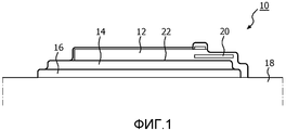
Фиг. 1 иллюстрирует поперечный разрез типичной ячейки cMUT согласно уровню техники.FIG. 1 illustrates a cross-sectional view of a typical cMUT cell according to the prior art.
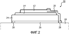
Фиг. 2 представляет собой поперечный разрез устройства cMUT, которое является акустически изолированным в соответствии с принципами настоящего изобретения.FIG. 2 is a cross-sectional view of a cMUT device that is acoustically insulated in accordance with the principles of the present invention.
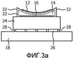
Фиг. 3a представляет собой схематическую иллюстрацию физики связывания устройства cMUT согласно настоящему изобретению.FIG. 3a is a schematic illustration of the binding physics of a cMUT device according to the present invention.
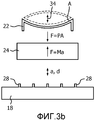
Фиг. 3b представляет собой перспективное изображение в разобранном виде схематической иллюстрации, представленной на Фиг. 3a, иллюстрирующей силы, участвующие в работе устройства.FIG. 3b is an exploded perspective view of the schematic illustration shown in FIG. 3a, illustrating the forces involved in the operation of the device.
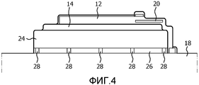
Фиг. 4 представляет собой поперечный разрез другого устройства MUT, акустически изолированного в соответствии с принципами настоящего изобретения.FIG. 4 is a cross-sectional view of another MUT device that is acoustically isolated in accordance with the principles of the present invention.
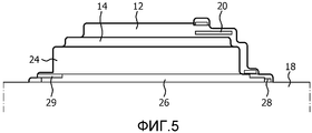
Фиг. 5 представляет собой поперечный разрез другого устройства MUT, акустически изолированного в соответствии с принципами настоящего изобретения.FIG. 5 is a cross-sectional view of another MUT device that is acoustically isolated in accordance with the principles of the present invention.
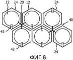
Фиг. 6 представляет собой вид сверху матрицы гексагональной ячейки cMUT, сконструированной в соответствии с настоящим изобретением и иллюстрирующей электрические соединения с ячейками.FIG. 6 is a plan view of a cMUT hexagonal cell array constructed in accordance with the present invention and illustrating electrical connections to cells.
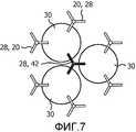
Фиг. 7 представляет собой вид сверху альтернативной технологии для создания электрических соединений с матрицей ячеек cMUT в соответствии с настоящим изобретением.FIG. 7 is a top view of an alternative technology for creating electrical connections with a cMUT cell array in accordance with the present invention.
Фиг. 8 представляет собой поперечный разрез cMUT, изготовленного на полупроводниковой подложке с цепью прикладной интегральной микросхемы (ASIC) для работы cMUT в соответствии с принципами настоящего изобретения.FIG. 8 is a cross-sectional view of a cMUT fabricated on a semiconductor substrate with an application integrated circuit (ASIC) for operating a cMUT in accordance with the principles of the present invention.
Обратимся сначала к Фиг. 1, где проиллюстрирован поперечный разрез типичного устройства cMUT 10 согласно уровню техники. cMUT 10 включает в себя верхний электрод 12, изготовленный из электропроводящего материала. Верхний электрод расположен на мембране 22 или он может сам по себе содержать мембрану. На этой иллюстрации мембрана образована из непроводящего материала, такого как нитрид кремния или диоксид кремния. Мембрана поддерживается вертикальными опорами на ее боковых кромках поверх пустоты или зазора 14. В данном варианте воплощения мембрана простирается через зазор, не касаясь дна внизу зазора. В других вариантах воплощения мембрана может быть специально установлена или смещена таким образом, чтобы она функционировала в режиме сжатия, когда центр мембраны находится в контакте с дном зазора. Проводник 20 подает электрические сигналы к верхнему электроду 12 и от него. Ниже зазора 14 находится нижний электрод 16. Электрические соединения с нижним электродом образованы из полупроводниковой подложки 18, на которой изготовлены ячейки cMUT матрицы преобразователя. Другие темные слои в этом варианте воплощения представляют собой слои изоляции, обычно образованные из нитрида кремния или диоксида кремния.Referring first to FIG. 1, where a cross-sectional view of a
Поскольку верхний электрод 12 и мембрана 22 вибрируют, при приведении их в действие передаваемым сигналом, желаемый акустический сигнал передается вверх от верхней поверхности верхнего электрода. Но силы, противодействующие этой силе, сопротивление силе волны акустического давления, вызванной платформой подложки, на которой изготовлены ячейки cMUT, заставляют акустические волны взаимодействовать с подложкой 18, где они могут двигаться назад через подложку и отражаться назад в ячейку cMUT, где они вызывают мешающие отраженные сигналы. Нежелательные акустические волны также могут перемещаться вбок к соседним ячейкам cMUT. Боковые волны могут достигать других ячеек cMUT при приеме сигнала и могут быть ложно приняты этими ячейками за принимаемые отраженные сигналы. Эти нежелательные сигналы, поступающие от подложки, могут быть интерпретированы в качестве сигналов помех, что снижает качество результирующего ультразвукового изображения.Since the
Фиг. 2 иллюстрирует поперечный разрез ячейки cMUT, сконструированной в соответствии с принципами настоящего изобретения. По идее, ячейка cMUT согласно настоящему изобретению может быть сконструирована в виде обычного cMUT, но с добавлением значительной массы под движущейся мембраной, либо в виде части нижнего электрода, или может быть прикреплена к нему. Эта масса может принимать форму пластины из очень плотного материала, с толщиной, достаточной для обеспечения основной реакции для приложенных акустических сил, со значительным меньшим перемещением, чем могло бы иметь место в подложке, если ячейка была бы непосредственно установлена на подложке. Массивные пластины для отдельных ячеек или групп ячеек сбоку акустически изолированы друг от друга для предотвращения бокового взаимодействия между одной массивной пластиной и другой. Является предпочтительным, чтобы массивная пластина была подвешена выше подложки на небольших опорах, таких как небольшие стойки с минимальной площадью поперечного сечения, для дополнительного снижения акустической связи с подложкой. В качестве альтернативы, массивная пластина может быть установлена на слое деформируемого материала. В дополнительном варианте воплощения массивная пластина может быть подвешена на небольших опорах, с пространством между пластиной и подложкой, соседней с опорами, заполненными деформируемым материалом, таким как полидиметилсилоксан (ПДМС), также известным как кремнекаучук.FIG. 2 illustrates a cross-sectional view of a cMUT cell constructed in accordance with the principles of the present invention. In principle, the cMUT cell according to the present invention can be constructed as a conventional cMUT, but with the addition of a significant mass under the moving membrane, either as part of the lower electrode, or can be attached to it. This mass can take the form of a plate of very dense material, with a thickness sufficient to provide the main reaction for the applied acoustic forces, with much less displacement than could occur in the substrate if the cell were directly mounted on the substrate. Massive plates for individual cells or groups of cells on the side are acoustically isolated from each other to prevent lateral interaction between one massive plate and another. It is preferred that the massive plate be suspended above the substrate on small supports, such as small racks with a minimum cross-sectional area, to further reduce acoustic coupling to the substrate. Alternatively, the massive plate may be mounted on a layer of deformable material. In a further embodiment, the massive plate may be suspended on small supports, with a space between the plate and the substrate adjacent to supports filled with a deformable material such as polydimethylsiloxane (PDMS), also known as silicon rubber.
В примере согласно Фиг. 2, верхний электрод 12 представляет собой проводник, такой как алюминиевая, вольфрамовая, поликремниевая мембрана или монокристаллический кремний. Верхний электрод 12 является деформируемым, а также функционирует в качестве мембраны устройства cMUT. Электрическое соединение с верхним электродом 12 создают за счет проводника 20, изготовленного, например, из вольфрама, алюминия, меди или поликремния. Верхний электрод 12 обычно может обладать толщиной 1-5 микрон, с диаметром по электроду 30-100 микрон. Форма ячеек cMUT может быть круглой или иметь другую форму, например гексагональную, прямоугольную или квадратную.In the example of FIG. 2, the
Зазор 14 расположен между верхним электродом 12 и массивной пластиной 24. Массивная пластина 24 сформирована таким образом, чтобы она обладала высокой жесткостью при частотах и толщинах, представляющих интерес. Пластина 24 будет тогда считаться маленькой, например, будет составлять одну десятую или менее от длины волны любого важного акустического режима распространения, при котором работает ячейка cMUT. Например, требования по массе и жесткости могут привести к использованию материала, обладающего высоким акустическим импедансом, например, акустическим импедансом более 40 мегарейл (Мрейл). Подходящие материалы для массивной пластины включают тантал (55 Мрейл), золото (64 Мрейл), молибден (63 Мрейл), вольфрам (101 Мрейл), медь (42 Мрейл) или хром (43 Мрейл), а также сплавы этих материалов. Один конкретный материал может представлять собой сплав титана и вольфрама, который легко можно применять в большинстве полупроводниковых производств. Выбор электропроводящего материала, такого как вольфрам, дополнительно дает возможность массивной пластине 24 служить в качестве нижнего электрода cMUT.The
Массивную пластину 24 не изготавливают непосредственно на подложке 26, но она опирается на несколько концевых стоек или краевых опор 28. Эти маленькие стойки 28 изготавливают из материалов, применяемых в процессе производства полупроводников, таких как кремний, нитрид кремния или оксид кремния. Проводящие материалы также можно использовать, если они надлежащим образом электрически изолированы. Типичная высота стоек составляет 3 микрон. Стойки должны быть достаточными, чтобы выдержать статические приложенные силы, которые в ином случае могут деформировать массивную пластину, должны быть еще достаточно небольшими, чтобы общая жесткость, добавленная к опорной пластине, была небольшой, по сравнению с инерционным сопротивлением, обеспечиваемым массой самой пластины при акустических частотах, представляющих интерес. Между стойками 28 находится второй зазор 26. Этот зазор может быть заполнен вакуумом, открыт для воздуха или заполнен деформируемым материалом, таким как кремнекаучук ПДМС. При заполнении второго зазора деформируемым материалом, таким как ПДМС, можно избежать загрязнения пространства нежелательными веществами. Матрица ячеек cMUT, такая как матрица, показанная на Фиг. 2, может быть изготовлена способом, основанным на осаждении слоев и травлении с потерей материала. Устройства также могут быть изготовлены с использованием технологий, основанных на склеивании плат или на сочетании этих способов.The
Фиг. 3a и 3b иллюстрируют разработанную концепцию настоящего изобретения. Фиг. 3a схематически иллюстрирует элементы cMUT согласно Фиг. 2, упакованные согласно той же конфигурации. Мембрана 22 установлена на опорах таким образом, чтобы она вибрировала за счет боковых опор 32 и была установлена на массивной пластине 24, как показано на Фиг. 3a. Верхний электрод 12 расположен поверх мембраны, а нижний электрод 16 расположен под мембраной. Массивная пластина 24 опирается на подложку 18 посредством множества маленьких стоек 28, разделенных пространствами, равными нижнему зазору 26.FIG. 3a and 3b illustrate the developed concept of the present invention. FIG. 3a schematically illustrates the cMUT elements of FIG. 2, packed according to the same configuration. The
Фиг. 3b показывает перспективное изображение данной сборки в разобранном виде и акустические силы, задействованные в работе cMUT. Мембрана 22 в ходе ультразвуковой передачи вибрирует вверх и вниз, как показано стрелкой 34 и кривыми выше и ниже нее. Поскольку мембрана вибрирует, она генерирует силу сжатия передаваемой звуковой волны с давлением P. Это давление оказывается областью мембраны A, а следовательно, генерируется сила, которая может быть рассчитана как F=PA. Сила этой волны сжатия направлена вниз через боковые опоры мембраны. Тело, на котором установлена опорная мембрана, - в данном случае, массивная пластина 24, противодействует силе акустического давления, генерируемой движущейся мембраной. Она делает это с инерцией своей массы. Эта противодействующая сила, выражена как F=Ma, - произведение большей массы M массивной пластины и ускорения «a», связанного с ее колебательным движением. Поскольку две силы равны и противоположны, а пластина является массивной, результат состоит в том, что компонент движения массивной пластины демонстрирует намного меньшее ускорение движения, представленное в уравнении как «a». Таким образом, сила сжатия cMUT уравновешивается не большим компонентом движения в подложке, а только много меньшим движением «d», связанным с ускорением «a», которое должно в нем содержаться. Это представлено на Фиг. 3a и 3b в виде массивной пластины 24, опирающейся на множестве неравномерно распределенных маленьких стойках 28 из деформируемого материала, которые работают на дополнительное ослабление передачи силы движения в подложку 18, в ответ на движение «d» с силой F', много меньшей, чем сила F, описанная выше. Таким образом, большое инерционное сопротивление массивной пластины в значительной степени предотвращает передачу нежелательных движений при акустических частотах в подложку.FIG. 3b shows an exploded perspective view of the assembly and the acoustic forces involved in the cMUT. The
Пример с расчетами для типичных материалов демонстрирует, как могут быть рассчитаны рабочие характеристики системы изоляции ячейки cMUT и определены желаемые размеры и свойства массивной пластины и наполнителя второго зазора. Предположим, например, что ячейка cMUT при передаче генерирует звуковое поле с уровнем максимального давления 1 МПа, при загрузке среды, эквивалентной воде, с акустическим импедансом 1,5 Мрейл, вибрацией при частоте f=20 МГц, - типичных параметров для зондового формирования изображения. Если ячейка имеет площадь A, то сила реакции на передней поверхности ячейки составляетThe calculation example for typical materials demonstrates how the performance of the cMUT cell insulation system can be calculated and the desired dimensions and properties of the massive plate and filler of the second gap determined. Suppose, for example, that a cMUT cell during transmission generates a sound field with a maximum pressure level of 1 MPa, when loading a medium equivalent to water, with an acoustic impedance of 1.5 Mere, vibration at a frequency of f = 20 MHz, typical parameters for probe imaging. If the cell has an area A, then the reaction force on the front surface of the cell is
1 MPa×A,1 MPa × A,
которая в обычной сборке cMUT может быть приложена непосредственно к подложке. Средняя амплитуда движения на передней поверхности преобразователя составляетwhich in a conventional cMUT assembly can be applied directly to the substrate. The average amplitude of motion on the front surface of the transducer is
1 MPa/(2·n·f·1,5 Мрейл)=>5 нм.1 MPa / (2 · n · f · 1.5 Mrayl) => 5 nm.
Масса реакционной пластины определяется по ее плотности, толщине и площади (как правило, примерно той же, что и площадь ячейки cMUT). Материал высокой плотности является предпочтительным для массивной пластины, поскольку в дальнейшем будет востребована меньшая толщина материала, что упрощает полупроводниковую обработку. В этом примере для материала пластины выбран вольфрам. Теперь, если мы рассматриваем слой вольфрама толщиной 3 мкм, действующий в качестве массивной пластины, масса на единицу площади представлена как плотность, умноженная на толщину,The mass of the reaction plate is determined by its density, thickness and area (as a rule, approximately the same as the area of the cMUT cell). High density material is preferable for a massive plate, since a smaller thickness of the material will be needed in the future, which simplifies semiconductor processing. In this example, tungsten is selected for the plate material. Now, if we consider a layer of tungsten with a thickness of 3 μm, acting as a massive plate, the mass per unit area is presented as the density multiplied by the thickness,
19300 кг/м3· 3·10-6м=>58 г/м2,19300 kg / m 3 · 3 · 10 -6 m => 58 g / m 2 ,
а результирующая амплитуда движения d пластины, при пренебрежении реакцией, вызванной деформируемым материалом под ней, получается из уравнения F=Ma, и для гармонического колебания при частоте f выражена какand the resulting amplitude of motion d of the plate, neglecting the reaction caused by the deformable material under it, is obtained from the equation F = Ma, and for harmonic oscillation at frequency f is expressed as
d=a/(4n2f2), и затемd = a / (4n 2 f 2 ), and then
d=F/(4·n2·f2)=0,06 нм.d = F / (4 · n 2 · f 2 ) = 0.06 nm.
Тогда как пространство между массивным слоем и подложкой может быть откачанным или наполненным воздухом, для обеспечения прочности при его изготовлении и использовании является желательным заполнять этот зазор мягким твердым материалом. Хотя акустическая изоляция с помощью вакуума или воздуха может быть иногда лучше, приемлемым выбором является стандартно применяемый каучук ПДМС. Мы можем рассчитать среднее давление, прикладываемое к подложке при этом движении, например, через 3-микронный слой каучука ПДМС, с акустическим импедансом Za равным 1 Мрейл и скоростью звука va равной 1000 м/сек.While the space between the massive layer and the substrate may be evacuated or filled with air, it is desirable to fill this gap with soft hard material to ensure strength in its manufacture and use. Although acoustic insulation with vacuum or air may sometimes be better, PDMS rubber is an acceptable choice. We can calculate the average pressure applied to the substrate during this movement, for example, through a 3-micron layer of PDMS rubber, with an acoustic impedance Z a equal to 1 Mereil and a sound speed v a equal to 1000 m / s.
Наведенное натяжение в PDMS представляет собой деформацию, деленную на толщину, в данном случае 0,06 нм/3000 нм=2·10-5, где жесткость PDMS настолько низка, что она существенно не влияет на амплитуду движения массивной пластины, и продольная жесткость составляетThe induced tension in the PDMS is the strain divided by the thickness, in this case 0.06 nm / 3000 nm = 2 · 10 -5 , where the stiffness of the PDMS is so low that it does not significantly affect the amplitude of motion of the massive plate, and the longitudinal stiffness is
C11=Za·va=1 ГПа.C 11 = Z a · v a = 1 GPa.
Поэтому напряжение или давление на подложке составляетTherefore, the voltage or pressure on the substrate is
P=C11·S=2·104 Па,P = C 11 · S = 2 · 10 4 Pa,
что по амплитуде в 50 раз меньше, чем напряжение в 1 МПа, которое может иметь место вне использования настоящего изобретения. Этот уровень функционирования приводит к коэффициенту затухания в 34 дБ для возбуждающей силы подложки под ней, применительно к нагрузке, вызванной cMUT. При других применениях могут быть желательны самые различные уровни рабочих характеристик. Например, в других вариантах воплощения настоящего изобретения могут являться приемлемыми уровни затухания в 50% (6 дБ), 66,67% (l0 дБ) или 90% (20 дБ) от акустической силы на подложке.which in amplitude is 50 times less than the voltage of 1 MPa, which may occur outside the use of the present invention. This level of operation results in a attenuation coefficient of 34 dB for the exciting force of the substrate underneath, as applied to the load caused by cMUT. In other applications, a wide variety of performance levels may be desirable. For example, in other embodiments of the present invention, attenuation levels of 50% (6 dB), 66.67% (l0 dB), or 90% (20 dB) of the acoustic force on the substrate may be acceptable.
Поскольку опорные структуры занимают не более примерно l/50 от площади поверхности, имеющей жесткость, сопоставимую с жесткостью массивного слоя, или значение жесткости, которая может быть значительно больше, если опорные структуры могут быть деформируемыми в целях их гибкости, может ожидаться именно этот уровень эффективности взаимодействия с подложкой. Если твердый деформируемый слой нанесен между массивным слоем и подложкой, то предпочтительным является использование деформируемых опор, вследствие чего акустическая сила, прилагаемая к подложке, будет равномерно приложена ко всей поверхности под ячейкой cMUT со стороны твердого слоя, что снизит вероятность образования поперечно распространяющихся волн, вызванных поперечным периодическим возбуждением через опорные структуры.Since the support structures occupy no more than about l / 50 of the surface area having a stiffness comparable to that of the massive layer, or a stiffness value that can be significantly greater if the support structures can be deformable for their flexibility, this level of efficiency can be expected interaction with the substrate. If a solid deformable layer is deposited between the bulk layer and the substrate, it is preferable to use deformable supports, as a result of which the acoustic force applied to the substrate will be uniformly applied to the entire surface under the cMUT cell from the side of the solid layer, which will reduce the likelihood of the formation of transversely propagating waves caused by transverse periodic excitation through the supporting structure.
Для альтернативного случая вакуумного зазора и нескольких небольших опорных стоек мы можем сделать аналогичный расчет. При условии 3-микронного зазора с движением на 0,06 нм на верхней поверхности и желании ограничить передаваемую силу величиной 2·104 Па с материалом стойки с жесткостью C11=290 ГПа (типичной для нитрида кремния),For an alternative case of a vacuum gap and several small support legs, we can do a similar calculation. Under the condition of a 3-micron gap with a movement of 0.06 nm on the upper surface and the desire to limit the transmitted force to 2 · 10 4 Pa with a rack material with rigidity C 11 = 290 GPa (typical for silicon nitride),
P=C11·S·Af=2·104 Па,P = C 11 · S · A f = 2 · 10 4 Pa,
где Af представляет собой долю площади поверхности, содержащей стойки, следовательно,where A f represents the fraction of the surface area containing the racks, therefore,
Af=2·104 Па/(290·109 Па·2·10-5)≅0,3%A f = 2 · 10 4 Pa / (290 · 10 9 Pa · 2 · 10 -5 ) ≅ 0.3%
Например, для круглой ячейки cMUT диаметром 30 мкм это требование может быть удовлетворено за счет трех прямых цилиндрических стоек диаметром 1 мкм, которые могут быть предельно допустимыми с точки зрения статической опоры. При использовании менее жесткого материала может быть обеспечено большее количество стоек. Например, при наличии диоксида кремния при жесткости 80 ГПа, с аналогичными размерами, может быть допустимо более 20 стоек, что даже больше, чем необходимо.For example, for a cMUT round cell with a diameter of 30 μm, this requirement can be satisfied by three straight cylindrical columns with a diameter of 1 μm, which can be extremely acceptable from the point of view of static support. When using less rigid material, more racks can be provided. For example, in the presence of silicon dioxide at a stiffness of 80 GPa, with similar dimensions, more than 20 racks may be permissible, which is even more than necessary.
Другой пример ячейки cMUT, сконструированной в соответствии с принципами настоящего изобретения, показан на Фиг. 4. В этом примере cMUT с его массивной пластиной 24 опирается на матрицу из множества маленьких стоек 28, изготовленных из структурного материала, который может представлять собой любой материал, уже используемый в процессе изготовления, такой как кремний, нитрид кремния, оксид кремния или любой из различных проводящих материалов, до тех пор, пока не будут установлены какие-либо электрические ограничения. Для того чтобы эти стойки механически поддерживали устройство, они должны быть достаточно многочисленными, чтобы они могли выдерживать статическую нагрузку давления воздуха и равномерно выдерживать любые приложенные снаружи статические силы, которые в ином случае могут деформировать массивную пластину. Примером такой силы является сила, которая может быть результатом выбора использования вакуума для зазоров 26 между стойками 28. Стойки должны быть достаточно небольшими, чтобы общая жесткость, придаваемая опорным пластинам, была мала, по сравнению с инерционным сопротивлением, обеспечиваемым при акустических частотах, представляющих интерес, за счет массы самой пластины. Является предпочтительным, чтобы стойки были расположены в виде матрицы для приблизительно равномерного распределения опор для cMUT и пластины по нижележащей подложке 18.Another example of a cMUT cell constructed in accordance with the principles of the present invention is shown in FIG. 4. In this example, cMUT with its
Другой пример ячейки cMUT, сконструированной в соответствии с принципами настоящего изобретения, показан на Фиг. 5. В этом примере cMUT с его массивной пластиной 24 опирается на деформируемые опоры 29, такие как кольцевая опора в случае круглого cMUT, вокруг периферии массивной пластины 24. В проиллюстрированном примере деформируемые опоры 29 обеспечивают деформируемую консольную опору с деформируемыми опорами 29, в свою очередь, опирающимися на опорное кольцо или матрицу стоек 28. Небольшие эффекты движения, не полностью устраненные за счет использования массивной пластины 24, смягчаются за счет упругой деформации опоры или опор 29.Another example of a cMUT cell constructed in accordance with the principles of the present invention is shown in FIG. 5. In this example, the cMUT with its
Фиг. 6 представляет собой вид сверху матрицы ячеек cMUT, в которой каждый cMUT является круглым, а массивные пластины 24 для ячеек имеют гексагональную форму. Каждый cMUT установлен на своей собственной отдельной пластине 24, а пластины 24 сбоку заизолированы друг от друга зазорами 40 между пластинами. Когда ячейки имеют форму, которая имеет различимые углы, часто является желательным изготавливать электрические соединения с электродами ячеек на углах. В этом примере примерные верхние электроды 12 ячеек cMUT соединены с опорным потенциалом или с заземлением посредством угловых соединений 20. Видно, в данном примере что одиночное соединение 20 разветвляется для соединения трех ячеек на их углах. В качестве сигнального электрода в данном примере обозначен нижний электрод (16 или 24). Соединения созданы и на других углах ячеек с образованием сигнальных соединений 42 с нижними электродами ячеек cMUT.FIG. 6 is a plan view of a cMUT cell array in which each cMUT is circular and the
Фиг. 7 представляет собой вид сверху матрицы ячеек cMUT 30, в которой каждый cMUT является круглым, а массивные пластины 24 для ячеек имеют также круглый и имеет тот же размер, что и верхний электрод или мембрана 12 или 22. Каждая ячейка cMUT и ее массивная пластина опираются на подложку посредством трех опор 28, которые также переносят на себе электрические соединения с электродами cMUT. В проиллюстрированной конфигурации опоры 28 разветвляются по трем направлениям, таким образом, чтобы поддерживать три различных cMUT 30. Опоры, обозначенные как 20, 28, несут на себе опорный потенциал или заземляют электрические соединения с верхними электродами 12 cMUT. Видно, что центральная опора, обозначенная как 28, 42, также поддерживает три cMUT и несет на себе отдельные сигнальные проводники, соединенные с нижними электродами 16, 24 трех cMUT, показанных на чертеже.FIG. 7 is a top view of the
Фиг. 8 представляет собой иллюстрацию частичного поперечного разреза матрицы cMUT, изготовленных в соответствии с настоящим изобретением. На этой иллюстрации слой 50 компонентов и соединений интегральной схемы образован на подложке 18 ИС. Слой 52 изоляции лежит поверх слоя интегральной схемы 50, а матрица cMUT образована на слое 52 изоляции, а не непосредственно на подложке 18. Электрические соединения выполнены от интегральной схемы слоя 50 через слой 52 изоляции к электродам cMUT, например, электрическое соединение 54 с проводником 20 cMU. На левой стороне чертежа пунктирно показана массивная пластина 24' соседней матрицы cMUT, отделенная от cMUT в центре чертежа зазором 40, который может быть заполнен воздухом или материалом, обычно используемым для нанесения покрытия на матрицу преобразователя, для обеспечения износостойкости, акустической связи со средой загрузки и/или фокусировки, - как правило, композитом кремнекаучука. Видно, что ячейки cMUT, опирающиеся на массивные пластины для изоляции движения, могут быть изготовлены на той же подложке и в ходе общей технологии производства полупроводниковых приборов, в виде микросхемы ASIC 50, которая функционирует и отвечает на сигналы, принимаемые ячейками преобразователя cMUT.FIG. 8 is a partial cross-sectional illustration of a cMUT matrix made in accordance with the present invention. In this illustration, an integrated circuit component layer 50 is formed on the
Claims (21)
(a) ячейки cMUT, причем каждая ячейка содержит:
мембрану ячейки;
опорную структуру мембраны;
верхний электрод, соединенный с мембраной ячейки;
зазор, обеспечивающий пространство, в котором движется мембрана ячейки; и
нижний электрод, используемый во взаимодействии с верхним электродом;
(b) множество массивных пластин, на которых установлены ячейки cMUT, причем каждая массивная пластина обладает силой инерции, которая, по существу, направлена противоположно силе акустического давления, генерируемой ячейкой cMUT, установленной на ней, во время передачи ячейкой cMUT, причем каждая массивная пластина и установленная на ней ячейка cMUT сбоку заизолированы движению от соседних массивных пластин с помощью зазора; и
(c) непрерывную подложку, на которой установлено множество массивных пластин и их ячейки cMUT.1. An array of cMUT cells of an ultrasonic transducer that are mounted on a plurality of massive plates that are mounted on a common substrate, comprising:
(a) cells cMUT, and each cell contains:
cell membrane;
membrane support structure;
an upper electrode connected to the cell membrane;
a gap providing the space in which the cell membrane moves; and
a lower electrode used in conjunction with the upper electrode;
(b) a plurality of massive plates on which cMUT cells are mounted, each massive plate having an inertia force that is essentially opposite to the acoustic pressure generated by the cMUT cell mounted on it during transmission of the cMUT cell, each massive plate and the cMUT cell installed on it is insulated to the side by movement from adjacent massive plates by a gap; and
(c) a continuous substrate on which a plurality of massive plates and their cMUT cells are mounted.
Applications Claiming Priority (3)
| Application Number | Priority Date | Filing Date | Title |
|---|---|---|---|
| US201161466172P | 2011-03-22 | 2011-03-22 | |
| US61/466,172 | 2011-03-22 | ||
| PCT/IB2012/051173 WO2012127360A2 (en) | 2011-03-22 | 2012-03-13 | Ultrasonic cmut with suppressed acoustic coupling to the substrate |
Publications (2)
| Publication Number | Publication Date |
|---|---|
| RU2013146954A RU2013146954A (en) | 2015-04-27 |
| RU2589272C2 true RU2589272C2 (en) | 2016-07-10 |
Family
ID=45937471
Family Applications (1)
| Application Number | Title | Priority Date | Filing Date |
|---|---|---|---|
| RU2013146954/28A RU2589272C2 (en) | 2011-03-22 | 2012-03-13 | Capacitive micromachined ultrasonic transducer with suppressed acoustic link with substrate |
Country Status (7)
| Country | Link |
|---|---|
| US (1) | US20130331705A1 (en) |
| EP (1) | EP2688686B1 (en) |
| JP (1) | JP5961246B2 (en) |
| CN (1) | CN103501922B (en) |
| BR (1) | BR112013023981A2 (en) |
| RU (1) | RU2589272C2 (en) |
| WO (1) | WO2012127360A2 (en) |
Cited By (1)
| Publication number | Priority date | Publication date | Assignee | Title |
|---|---|---|---|---|
| RU2769757C2 (en) * | 2017-09-22 | 2022-04-05 | Конинклейке Филипс Н.В. | Ultrasonic converter and method of controlling it |
Families Citing this family (36)
| Publication number | Priority date | Publication date | Assignee | Title |
|---|---|---|---|---|
| IN2014CN04975A (en) * | 2011-12-20 | 2015-09-18 | Koninkl Philips Nv | |
| GB2513884B (en) | 2013-05-08 | 2015-06-17 | Univ Bristol | Method and apparatus for producing an acoustic field |
| DE102013223695B4 (en) * | 2013-11-20 | 2016-09-22 | Fraunhofer-Gesellschaft zur Förderung der angewandten Forschung e.V. | METHOD FOR PRODUCING A CAPACITIVE ULTRASONIC TRANSDUCER AND ARRANGEMENT OF A MULTIPLE OF CAPACITIVE ULTRASONIC TRANSDUCERS |
| KR102155695B1 (en) * | 2014-02-12 | 2020-09-21 | 삼성전자주식회사 | Electro acoustic transducer |
| GB2530036A (en) | 2014-09-09 | 2016-03-16 | Ultrahaptics Ltd | Method and apparatus for modulating haptic feedback |
| US10674999B2 (en) * | 2014-11-25 | 2020-06-09 | Koninklijke Philips N.V. | Ultrasound system and method |
| US9841819B2 (en) | 2015-02-20 | 2017-12-12 | Ultrahaptics Ip Ltd | Perceptions in a haptic system |
| CA2976319C (en) | 2015-02-20 | 2023-06-27 | Ultrahaptics Ip Limited | Algorithm improvements in a haptic system |
| JP6925286B2 (en) * | 2015-06-30 | 2021-08-25 | コーニンクレッカ フィリップス エヌ ヴェKoninklijke Philips N.V. | Ultrasonic system and ultrasonic pulse transmission method |
| JP6932085B2 (en) | 2015-07-02 | 2021-09-08 | コーニンクレッカ フィリップス エヌ ヴェKoninklijke Philips N.V. | Multimode Capacitive Micromachine Ultrasonic Transducers and Related Devices, Systems and Methods |
| DE102015212683A1 (en) * | 2015-07-07 | 2017-01-12 | Robert Bosch Gmbh | Sound transducer and installation arrangement with a sound transducer |
| US10818162B2 (en) | 2015-07-16 | 2020-10-27 | Ultrahaptics Ip Ltd | Calibration techniques in haptic systems |
| US9751108B2 (en) * | 2015-07-31 | 2017-09-05 | Texas Instruments Incorporated | Extended range ultrasound transducer |
| EP3338113B1 (en) | 2015-11-24 | 2021-08-25 | Halliburton Energy Services, Inc. | Ultrasonic transducer with suppressed lateral mode |
| KR20190022644A (en) | 2016-06-20 | 2019-03-06 | 버터플라이 네트워크, 인크. | Electrical contact arrangement for a microfabricated ultrasonic transducer |
| US10268275B2 (en) | 2016-08-03 | 2019-04-23 | Ultrahaptics Ip Ltd | Three-dimensional perceptions in haptic systems |
| US20190357882A1 (en) * | 2016-11-22 | 2019-11-28 | Koninklijke Philips N.V. | Ultrasound device and acoustic component for use in such a device |
| US10943578B2 (en) | 2016-12-13 | 2021-03-09 | Ultrahaptics Ip Ltd | Driving techniques for phased-array systems |
| US11531395B2 (en) | 2017-11-26 | 2022-12-20 | Ultrahaptics Ip Ltd | Haptic effects from focused acoustic fields |
| US11704983B2 (en) | 2017-12-22 | 2023-07-18 | Ultrahaptics Ip Ltd | Minimizing unwanted responses in haptic systems |
| US10656007B2 (en) | 2018-04-11 | 2020-05-19 | Exo Imaging Inc. | Asymmetrical ultrasound transducer array |
| US10648852B2 (en) | 2018-04-11 | 2020-05-12 | Exo Imaging Inc. | Imaging devices having piezoelectric transceivers |
| WO2019211616A1 (en) | 2018-05-02 | 2019-11-07 | Ultrahaptics Limited | Blocking plate structure for improved acoustic transmission efficiency |
| US11098951B2 (en) | 2018-09-09 | 2021-08-24 | Ultrahaptics Ip Ltd | Ultrasonic-assisted liquid manipulation |
| US11550395B2 (en) | 2019-01-04 | 2023-01-10 | Ultrahaptics Ip Ltd | Mid-air haptic textures |
| US11842517B2 (en) | 2019-04-12 | 2023-12-12 | Ultrahaptics Ip Ltd | Using iterative 3D-model fitting for domain adaptation of a hand-pose-estimation neural network |
| CN114728311A (en) | 2019-09-12 | 2022-07-08 | 艾科索成像公司 | MUT coupling efficiency and bandwidth via edge notches, virtual pivots, and free boundaries |
| JP2022551944A (en) | 2019-10-13 | 2022-12-14 | ウルトラリープ リミテッド | Dynamic capping with virtual microphones |
| US11374586B2 (en) | 2019-10-13 | 2022-06-28 | Ultraleap Limited | Reducing harmonic distortion by dithering |
| US11715453B2 (en) | 2019-12-25 | 2023-08-01 | Ultraleap Limited | Acoustic transducer structures |
| US11816267B2 (en) | 2020-06-23 | 2023-11-14 | Ultraleap Limited | Features of airborne ultrasonic fields |
| WO2022058738A1 (en) | 2020-09-17 | 2022-03-24 | Ultraleap Limited | Ultrahapticons |
| CN115968272A (en) * | 2021-03-29 | 2023-04-14 | 艾科索成像公司 | Trench for reducing crosstalk in MUT arrays |
| US11819881B2 (en) | 2021-03-31 | 2023-11-21 | Exo Imaging, Inc. | Imaging devices having piezoelectric transceivers with harmonic characteristics |
| US11951512B2 (en) | 2021-03-31 | 2024-04-09 | Exo Imaging, Inc. | Imaging devices having piezoelectric transceivers with harmonic characteristics |
| WO2022254205A1 (en) * | 2021-06-02 | 2022-12-08 | Ultraleap Limited | Electromechanical transducer mount |
Citations (5)
| Publication number | Priority date | Publication date | Assignee | Title |
|---|---|---|---|---|
| RU2117415C1 (en) * | 1994-05-31 | 1998-08-10 | Шанаурин Александр Михайлович | Electrostatic capacitor converter |
| US7303530B2 (en) * | 2003-05-22 | 2007-12-04 | Siemens Medical Solutions Usa, Inc. | Transducer arrays with an integrated sensor and methods of use |
| US7408283B2 (en) * | 2003-12-29 | 2008-08-05 | General Electric Company | Micromachined ultrasonic transducer cells having compliant support structure |
| RU2404711C2 (en) * | 2005-04-25 | 2010-11-27 | Конинклейке Филипс Электроникс Н.В. | Method and device for continuous visualisation by system of ultrasonic converter |
| US7888709B2 (en) * | 2004-09-15 | 2011-02-15 | Sonetics Ultrasound, Inc. | Capacitive micromachined ultrasonic transducer and manufacturing method |
Family Cites Families (18)
| Publication number | Priority date | Publication date | Assignee | Title |
|---|---|---|---|---|
| US6262946B1 (en) | 1999-09-29 | 2001-07-17 | The Board Of Trustees Of The Leland Stanford Junior University | Capacitive micromachined ultrasonic transducer arrays with reduced cross-coupling |
| US6443901B1 (en) | 2000-06-15 | 2002-09-03 | Koninklijke Philips Electronics N.V. | Capacitive micromachined ultrasonic transducers |
| US6862254B2 (en) | 2000-10-19 | 2005-03-01 | Sensant Corporation | Microfabricated ultrasonic transducer with suppressed substrate modes |
| US6669644B2 (en) | 2001-07-31 | 2003-12-30 | Koninklijke Philips Electronics N.V. | Micro-machined ultrasonic transducer (MUT) substrate that limits the lateral propagation of acoustic energy |
| US6831394B2 (en) | 2002-12-11 | 2004-12-14 | General Electric Company | Backing material for micromachined ultrasonic transducer devices |
| US20040190377A1 (en) * | 2003-03-06 | 2004-09-30 | Lewandowski Robert Stephen | Method and means for isolating elements of a sensor array |
| US7545075B2 (en) | 2004-06-04 | 2009-06-09 | The Board Of Trustees Of The Leland Stanford Junior University | Capacitive micromachined ultrasonic transducer array with through-substrate electrical connection and method of fabricating same |
| US8247945B2 (en) * | 2005-05-18 | 2012-08-21 | Kolo Technologies, Inc. | Micro-electro-mechanical transducers |
| CA2608164A1 (en) * | 2005-06-17 | 2006-12-21 | Kolo Technologies, Inc. | Micro-electro-mechanical transducer having an insulation extension |
| JP4724505B2 (en) * | 2005-09-09 | 2011-07-13 | 株式会社日立製作所 | Ultrasonic probe and manufacturing method thereof |
| US7741686B2 (en) * | 2006-07-20 | 2010-06-22 | The Board Of Trustees Of The Leland Stanford Junior University | Trench isolated capacitive micromachined ultrasonic transducer arrays with a supporting frame |
| RU2449418C2 (en) * | 2006-09-25 | 2012-04-27 | Конинклейке Филипс Электроникс Н.В. | Interconnection by flip-chip technique through open-end holes in chip |
| US7843022B2 (en) * | 2007-10-18 | 2010-11-30 | The Board Of Trustees Of The Leland Stanford Junior University | High-temperature electrostatic transducers and fabrication method |
| US8207652B2 (en) * | 2009-06-16 | 2012-06-26 | General Electric Company | Ultrasound transducer with improved acoustic performance |
| JP5578810B2 (en) * | 2009-06-19 | 2014-08-27 | キヤノン株式会社 | Capacitance type electromechanical transducer |
| KR20110002630A (en) * | 2009-07-02 | 2011-01-10 | 삼성전자주식회사 | Operation method for camera of portable device and apparatus using the same |
| JP5495918B2 (en) * | 2009-07-24 | 2014-05-21 | キヤノン株式会社 | Electromechanical transducer and method for producing electromechanical transducer |
| US8455289B1 (en) * | 2011-12-02 | 2013-06-04 | Texas Instruments Incorporated | Low frequency CMUT with thick oxide |
-
2012
- 2012-03-13 WO PCT/IB2012/051173 patent/WO2012127360A2/en active Application Filing
- 2012-03-13 RU RU2013146954/28A patent/RU2589272C2/en not_active IP Right Cessation
- 2012-03-13 CN CN201280014348.5A patent/CN103501922B/en active Active
- 2012-03-13 EP EP12713338.7A patent/EP2688686B1/en active Active
- 2012-03-13 US US14/000,891 patent/US20130331705A1/en not_active Abandoned
- 2012-03-13 JP JP2014500501A patent/JP5961246B2/en active Active
- 2012-03-13 BR BR112013023981A patent/BR112013023981A2/en not_active Application Discontinuation
Patent Citations (5)
| Publication number | Priority date | Publication date | Assignee | Title |
|---|---|---|---|---|
| RU2117415C1 (en) * | 1994-05-31 | 1998-08-10 | Шанаурин Александр Михайлович | Electrostatic capacitor converter |
| US7303530B2 (en) * | 2003-05-22 | 2007-12-04 | Siemens Medical Solutions Usa, Inc. | Transducer arrays with an integrated sensor and methods of use |
| US7408283B2 (en) * | 2003-12-29 | 2008-08-05 | General Electric Company | Micromachined ultrasonic transducer cells having compliant support structure |
| US7888709B2 (en) * | 2004-09-15 | 2011-02-15 | Sonetics Ultrasound, Inc. | Capacitive micromachined ultrasonic transducer and manufacturing method |
| RU2404711C2 (en) * | 2005-04-25 | 2010-11-27 | Конинклейке Филипс Электроникс Н.В. | Method and device for continuous visualisation by system of ultrasonic converter |
Cited By (1)
| Publication number | Priority date | Publication date | Assignee | Title |
|---|---|---|---|---|
| RU2769757C2 (en) * | 2017-09-22 | 2022-04-05 | Конинклейке Филипс Н.В. | Ultrasonic converter and method of controlling it |
Also Published As
| Publication number | Publication date |
|---|---|
| US20130331705A1 (en) | 2013-12-12 |
| BR112013023981A2 (en) | 2016-12-13 |
| CN103501922B (en) | 2016-08-17 |
| WO2012127360A3 (en) | 2013-04-25 |
| JP5961246B2 (en) | 2016-08-02 |
| CN103501922A (en) | 2014-01-08 |
| RU2013146954A (en) | 2015-04-27 |
| WO2012127360A2 (en) | 2012-09-27 |
| JP2014510489A (en) | 2014-04-24 |
| EP2688686B1 (en) | 2022-08-17 |
| EP2688686A2 (en) | 2014-01-29 |
Similar Documents
| Publication | Publication Date | Title |
|---|---|---|
| RU2589272C2 (en) | Capacitive micromachined ultrasonic transducer with suppressed acoustic link with substrate | |
| US9454954B2 (en) | Ultra wide bandwidth transducer with dual electrode | |
| KR101236118B1 (en) | Reconfigurable linear sensor arrays for reduced channel count | |
| US9073085B2 (en) | Electromechanical transducer | |
| US20050075572A1 (en) | Focusing micromachined ultrasonic transducer arrays and related methods of manufacture | |
| JP5087617B2 (en) | Capacitive transducer and ultrasonic imaging apparatus | |
| US20120176002A1 (en) | Acoustic transducer and method of driving the same | |
| JP5643191B2 (en) | Ultrasonic probe and ultrasonic imaging apparatus | |
| CN112893067B (en) | Multi-cell transducer | |
| KR101593994B1 (en) | High power ultrasonic transducer | |
| JP5026770B2 (en) | Ultrasonic probe and ultrasonic diagnostic apparatus | |
| JP2013165753A (en) | Ultrasonic probe and ultrasonic diagnostic apparatus using the same | |
| WO2018037730A1 (en) | Capacitive micromachined ultrasonic transducer and ultrasonic imaging apparatus comprising same | |
| JP2006174992A (en) | Ultrasonic probe | |
| JP7024550B2 (en) | Ultrasonic sensor and ultrasonic device | |
| JP6390428B2 (en) | Ultrasonic transducer cell, ultrasonic probe, and control method of ultrasonic transducer cell | |
| JP6206033B2 (en) | Ultrasonic transducer device and ultrasonic measurement apparatus | |
| JP2020080497A (en) | Ultrasonic device and ultrasonic sensor | |
| CN113120854B (en) | Backing type high-frequency broadband PMUT unit and PMUT array | |
| US20210361260A1 (en) | Ultrasonic transducer array having varying cavity diameter profile | |
| JP2006174991A (en) | Ultrasonic probe | |
| Shabanimotlagh et al. | Optimizing the directivity of piezoelectric matrix transducer elements mounted on an ASIC | |
| JP2019176292A (en) | Ultrasonic sensor and ultrasonic device | |
| JP2006262149A (en) | Ultrasonic probe and ultrasonic diagnostic device | |
| JP2018088636A (en) | Ultrasonic device, ultrasonic apparatus, and thickness design method |
Legal Events
| Date | Code | Title | Description |
|---|---|---|---|
| MM4A | The patent is invalid due to non-payment of fees |
Effective date: 20190314 |