JP5495918B2 - Electromechanical transducer and method for producing electromechanical transducer - Google Patents
Electromechanical transducer and method for producing electromechanical transducer Download PDFInfo
- Publication number
- JP5495918B2 JP5495918B2 JP2010096557A JP2010096557A JP5495918B2 JP 5495918 B2 JP5495918 B2 JP 5495918B2 JP 2010096557 A JP2010096557 A JP 2010096557A JP 2010096557 A JP2010096557 A JP 2010096557A JP 5495918 B2 JP5495918 B2 JP 5495918B2
- Authority
- JP
- Japan
- Prior art keywords
- substrate
- groove
- membrane
- electromechanical
- electrode
- Prior art date
- Legal status (The legal status is an assumption and is not a legal conclusion. Google has not performed a legal analysis and makes no representation as to the accuracy of the status listed.)
- Active
Links
Images


Classifications
-
- H—ELECTRICITY
- H04—ELECTRIC COMMUNICATION TECHNIQUE
- H04R—LOUDSPEAKERS, MICROPHONES, GRAMOPHONE PICK-UPS OR LIKE ACOUSTIC ELECTROMECHANICAL TRANSDUCERS; DEAF-AID SETS; PUBLIC ADDRESS SYSTEMS
- H04R31/00—Apparatus or processes specially adapted for the manufacture of transducers or diaphragms therefor
-
- B—PERFORMING OPERATIONS; TRANSPORTING
- B06—GENERATING OR TRANSMITTING MECHANICAL VIBRATIONS IN GENERAL
- B06B—METHODS OR APPARATUS FOR GENERATING OR TRANSMITTING MECHANICAL VIBRATIONS OF INFRASONIC, SONIC, OR ULTRASONIC FREQUENCY, e.g. FOR PERFORMING MECHANICAL WORK IN GENERAL
- B06B1/00—Methods or apparatus for generating mechanical vibrations of infrasonic, sonic, or ultrasonic frequency
- B06B1/02—Methods or apparatus for generating mechanical vibrations of infrasonic, sonic, or ultrasonic frequency making use of electrical energy
- B06B1/0292—Electrostatic transducers, e.g. electret-type
-
- H—ELECTRICITY
- H02—GENERATION; CONVERSION OR DISTRIBUTION OF ELECTRIC POWER
- H02N—ELECTRIC MACHINES NOT OTHERWISE PROVIDED FOR
- H02N1/00—Electrostatic generators or motors using a solid moving electrostatic charge carrier
- H02N1/06—Influence generators
- H02N1/08—Influence generators with conductive charge carrier, i.e. capacitor machines
-
- Y—GENERAL TAGGING OF NEW TECHNOLOGICAL DEVELOPMENTS; GENERAL TAGGING OF CROSS-SECTIONAL TECHNOLOGIES SPANNING OVER SEVERAL SECTIONS OF THE IPC; TECHNICAL SUBJECTS COVERED BY FORMER USPC CROSS-REFERENCE ART COLLECTIONS [XRACs] AND DIGESTS
- Y10—TECHNICAL SUBJECTS COVERED BY FORMER USPC
- Y10T—TECHNICAL SUBJECTS COVERED BY FORMER US CLASSIFICATION
- Y10T29/00—Metal working
- Y10T29/49—Method of mechanical manufacture
- Y10T29/49002—Electrical device making
- Y10T29/49005—Acoustic transducer
Description
本発明は、超音波トランスデューサなどの電気機械変換装置及びその作製方法に関する。 The present invention relates to an electromechanical transducer such as an ultrasonic transducer and a manufacturing method thereof.
超音波トランスデューサは、電気信号から超音波への変換、超音波から電気信号への変換を行うものであり、医用イメージング、非破壊検査用の探触子として用いられる。超音波トランスデューサの一形態に、容量性マイクロマシン加工超音波トランスデューサ(Capacitive Micromachined Ultrasound Transducer:CMUT)がある。CMUTは、例えば、下部電極を有する基板と、この基板上に形成された支持部で支えられたメンブレンと、上部電極とで構成される。1つのキャビティは、下部電極、メンブレン、上部電極、支持部で画されて形成される。CMUTは、下部電極と上部電極間に印加する電圧でメンブレンを振動させ、音波を放出する。また、受け取った音波でメンブレンが振動させられ、下部電極と上部電極間の静電容量の変化により音波が検出される。 The ultrasonic transducer performs conversion from an electric signal to an ultrasonic wave and conversion from an ultrasonic wave to an electric signal, and is used as a probe for medical imaging and nondestructive inspection. One form of the ultrasonic transducer is a capacitive micromachined ultrasonic transducer (CMUT). The CMUT includes, for example, a substrate having a lower electrode, a membrane supported by a support portion formed on the substrate, and an upper electrode. One cavity is defined by a lower electrode, a membrane, an upper electrode, and a support part. The CMUT emits sound waves by vibrating the membrane with a voltage applied between the lower electrode and the upper electrode. Further, the membrane is vibrated by the received sound wave, and the sound wave is detected by a change in capacitance between the lower electrode and the upper electrode.
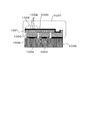
従来、CMUTは、いわゆるサーフェスマイクロマシニング、バルクマイクロマシニングなどを利用して作製されてきた。また、配線方法として、シリコン基板上の複数のメンブレンとキャビティを1つのエレメントとし、前記シリコン基板そのものを下部電極及び貫通配線として回路基板にエレメントを接続する方法がある(特許文献1参照)。この方法を図6で説明する。CMUT1007は複数のエレメント1008で構成され、エレメントを1つのユニットとして超音波の送受信を行う。エレメント1008は、上部電極1000、メンブレン1001、キャビティ1002、下部電極1003で構成されている。隣り合うエレメント1008同士を電気的に分離して絶縁を図るため、溝1004が形成されている。CMUT1007はバンプ1005によりASIC基板1006と接続されている。
Conventionally, the CMUT has been manufactured using so-called surface micromachining, bulk micromachining and the like. As a wiring method, there is a method in which a plurality of membranes and cavities on a silicon substrate are used as one element, and the silicon substrate itself is used as a lower electrode and a through wiring to connect the element to the circuit board (see Patent Document 1). This method will be described with reference to FIG. The CMUT 1007 includes a plurality of
上記従来のCMUTは、1つのキャビティ又は複数のキャビティの集合体からなる単位素子であるエレメントを電気的に分離するために数百ミクロンの幅を有する分離溝を必要とする。しかし、この分離溝の部分にはキャビティを配置できないため、基板の単位面積あたりに配置できるキャビティの数が少なくなり、フィルファクター(本明細書では、基板の単位面積あたりの電気機械変換部の占有率を意味する)が低下する。従って、デバイス全体としての感度が低下し易い。 The conventional CMUT is an isolation trench having a width of several hundred microns in order to electrically isolate the element is a unit element consisting of a collection of one cavity or a plurality of cavities required. However, since the cavity cannot be arranged in the separation groove portion, the number of cavities that can be arranged per unit area of the substrate is reduced, and the fill factor (in this specification, the occupation of the electromechanical conversion unit per unit area of the substrate) is reduced. (Meaning rate) decreases. Therefore, the sensitivity of the entire device is likely to decrease.
上記課題に鑑み、本発明の電気機械変換装置は、導電性の基板と、前記基板の第1の面に配置された複数の静電容量型等の電気機械変換部と、を有する。前記基板には、前記複数の電気機械変換部を互いに電気的に分離するために、前記基板の前記第1の面とは反対側の第2の面側から前記基板の第1の面側へ伸びる溝が形成されている。そして、前記基板の第1の面側の前記溝の幅は、前記基板の第2の面側の前記溝の幅より狭くなっている。 In view of the above problems, an electromechanical conversion device of the present invention includes a conductive substrate and a plurality of capacitance type electromechanical conversion units disposed on a first surface of the substrate. In the substrate, in order to electrically isolate the plurality of electromechanical transducers from each other, the second surface side opposite to the first surface of the substrate is from the first surface side of the substrate. An extending groove is formed. The width of the groove on the first surface side of the substrate is narrower than the width of the groove on the second surface side of the substrate.
また、上記課題に鑑み、本発明の電気機械変換装置の作製方法は次の工程を含む。シリコン基板に溝をアルカリウェットエッチングで形成し、互いに分離された複数の第1の電極を形成する工程。前記第1の電極に対向するキャビティを形成する工程。前記キャビティに対向するメンブレンを形成する工程。前記メンブレン上に第2の電極を形成する工程。前記アルカリウェットエッチングにより互いに分離された複数の第1の電極を形成する工程は、シリコン基板に溝を複数回のドライエッチングで形成し、互いに分離された複数の第1の電極を形成する工程に置き換えることもできる。 Moreover, in view of the said subject, the manufacturing method of the electromechanical transducer of this invention includes the following process. Forming a plurality of first electrodes separated from each other by forming grooves in the silicon substrate by alkali wet etching; Forming a cavity facing the first electrode; Forming a membrane facing the cavity; Forming a second electrode on the membrane; The step of forming a plurality of first electrodes separated from each other by the alkali wet etching is a step of forming a plurality of first electrodes separated from each other by forming a groove in a silicon substrate by a plurality of dry etchings. It can also be replaced.
本発明によれば、前記基板の第1の面側の溝の幅を第2の面側の溝の幅よりも狭くすることで、第1の面側には複数の電気機械変換部を比較的高い密度で配置することができる。そして、第1の面側から第2の面側に向かって溝の幅を大きくすることで分離溝全体としては十分な幅を確保しているので、電気機械変換部間の電気的分離を確保し、寄生容量を抑えることができる。その結果、第1の面側の溝の幅が小さいことによる感度低下を抑えることができる。また、感度低下を抑えつつ第1の面側の溝の幅を狭くできるので、電気機械変換部を高い密度で配置することが可能となり、フィルファクターの向上が可能となる。この点からも、CMUTなどの電気機械変換装置の感度を向上することができる。言い換えれば、本発明により、電気機械変換部間の寄生容量の低減と電気機械変換装置の信号出力の向上を両立させることができる。 According to the present invention, a plurality of electromechanical transducers are compared on the first surface side by making the width of the groove on the first surface side of the substrate narrower than the width of the groove on the second surface side. Can be arranged at a high density. And since the width of the groove is increased from the first surface side toward the second surface side to ensure a sufficient width for the entire separation groove, electrical separation between the electromechanical converters is ensured. In addition, parasitic capacitance can be suppressed. As a result, it is possible to suppress a decrease in sensitivity due to the small width of the groove on the first surface side. In addition, since the width of the groove on the first surface side can be reduced while suppressing a decrease in sensitivity, it is possible to arrange the electromechanical conversion portions with a high density and to improve the fill factor. Also from this point, the sensitivity of an electromechanical transducer such as CMUT can be improved. In other words, according to the present invention, it is possible to simultaneously reduce the parasitic capacitance between the electromechanical converters and improve the signal output of the electromechanical converter.
以下、本発明の実施形態について説明する。本発明の電気機械変換装置及びその作製方法の特徴は次の点にある。すなわち、複数の電気機械変換部の配置に対応して、導電性基板の第1の面側の幅(底部の幅ともいう)が第2の面側の幅(開口部の幅ともいう)よりも狭い溝を形成して該基板を複数の部分に分割し、電極を兼ねる該基板の複数の部分を互いに絶縁する。 Hereinafter, embodiments of the present invention will be described. The features of the electromechanical transducer of the present invention and the manufacturing method thereof are as follows. That is, the width on the first surface side (also referred to as the width of the bottom portion) of the conductive substrate is greater than the width on the second surface side (also referred to as the width of the opening) corresponding to the arrangement of the plurality of electromechanical conversion portions. A narrow groove is formed to divide the substrate into a plurality of portions, and the portions of the substrate that also serve as electrodes are insulated from each other.
上記考え方に基づき、本発明の電気機械変換装置及びその作製方法の基本的な形態は、課題を解決するための手段のところで述べた様な構成を有する。この基本的な形態を基に、以下に述べる様な実施形態が可能である。 Based on the above concept, the basic form of the electromechanical transducer of the present invention and the manufacturing method thereof has the configuration as described in the means for solving the problems. On the basis of this basic form, the following embodiments are possible.
前記溝は、例えば、開口部から底部に向かって連続的又は非連続的に小さくなる(第1の面側から該第1の面とは反対側の第2の面側に向かって連続的又は非連続的に広くなる)断面形状を有することができる。こうした構造は、静電容量型等の電気機械変換部間の寄生容量の低減と電気機械変換部のフィルファクターの向上の観点から、好ましいものである。また、シリコン基板に溝をアルカリウェットエッチングで形成する方法で、容易に実現できる構造である。この方法では、基板面に対して54.7度の角度を成す溝斜面が形成できるので、基板の厚さとエッチング用マスクの開口部の幅を適切に設定することで、上記の如き溝を容易に形成できる(後述の実施例2参照)。この場合、溝の側壁は、基板に対して傾斜した平面状となる。 The groove, for example, continuously or discontinuously decreases from the opening to the bottom (continuously from the first surface side to the second surface side opposite to the first surface or It can have a cross-sectional shape that is discontinuously widened. Such a structure is preferable from the viewpoint of reducing the parasitic capacitance between the electromechanical conversion units of the electrostatic capacity type and the like and improving the fill factor of the electromechanical conversion unit. Further, this structure can be easily realized by a method of forming a groove in a silicon substrate by alkali wet etching. In this method, a groove slope having an angle of 54.7 degrees with respect to the substrate surface can be formed. Therefore, by appropriately setting the thickness of the substrate and the width of the opening of the etching mask, the groove as described above can be easily formed. (See Example 2 described later). In this case, the side wall of the groove has a planar shape inclined with respect to the substrate.
前記溝の側壁を階段状にすることもできる。こうした構造は、複数回のドライエッチング、つまりドライの多段エッチングで容易に作製できる。すなわち、複数の電気機械変換部の配置に対応した適当なパターンでマスクをシリコン基板の底面に形成して1回目のドライエッチングを実行した後、マスクの開口部を適当に拡大して次のドライエッチングを実行する。この様なエッチング工程を、溝を階段状に深くしつつ基板の他方の面に達するまで繰り返すことで、側壁が階段状の溝を形成できる。この方法でも、底部の幅が開口部よりも小さい溝形状にすることができる。 The side wall of the groove may be stepped. Such a structure can be easily manufactured by a plurality of dry etchings, that is, dry multi-stage etching. That is, after a mask is formed on the bottom surface of the silicon substrate with an appropriate pattern corresponding to the arrangement of the plurality of electromechanical transducers and the first dry etching is performed, the mask opening is appropriately enlarged and the next dry etching is performed. Perform etching. By repeating such an etching process until the groove reaches the other surface of the substrate while making the groove deeper in a step shape, a groove having a stepped sidewall can be formed. Even in this method, it is possible to form a groove having a bottom width smaller than that of the opening.
以下、本発明の複数の実施例を、図面を参照して詳細に説明する。ただし、本発明はこれら実施例の具体的形態に限定されるものではない。
(実施例1)
実施例1を、図1を参照して説明する。実施例1は、溝でエレメントが分離されたSi基板からなる静電容量型超音波トランスデューサであって、メンブレン105をSOI(Silicon−on−insulator)基板の接合により作製したデバイスに関する。本実施例の電気機械変換装置の断面図の図1(a)に示す様に、本電気機械変換装置100は、回路基板101、シリコン基板103で構成される。回路基板101は、シリコン基板103の真下に配置されている。
Hereinafter, a plurality of embodiments of the present invention will be described in detail with reference to the drawings. However, the present invention is not limited to the specific forms of these examples.
Example 1
Example 1 will be described with reference to FIG. Example 1 relates to a capacitive ultrasonic transducer composed of a Si substrate in which elements are separated by grooves, and a
図1(a)の上面図である図1(b)に示す様に、本実施例の電気機械変換装置100は4×4のエレメント104で構成されている。図1(b)の104で示す領域が1エレメントである。ここで、上記静電容量型の電気機械変換部であるエレメント104は、超音波を送受信する1ユニットである。1エレメントにつき、1つの下部電極108とそれに続く貫通配線109が配置されている。ここでは、4×4個のエレメント104が配列されているが、これに限定されない。図1(b)の一部を拡大した図である図1(c)と図1(c)のA−A’断面図である図1(a)を用いて、エレメント104を説明する。基板103の第1の面である一方の面に配置されたエレメント104は、メンブレン105、キャビティ106、上部電極107、下部電極108などで構成される。それぞれの材質は、メンブレンがSi、キャビティ周りの材料(メンブレン側を除く)がSiO2、上部電極がAl、下部電極がSi、貫通配線である下部引き出し配線がSiである。Si基板103と回路基板101とは、はんだ110と電極パッド116を介して接合されている。この様に、本実施例では、電気機械変換部であるエレメント104は、支持部と、支持部に設けられたメンブレンと、メンブレンと対向して設けられた第1の電極である下部電極と、メンブレン上に設けられた第2の電極である上部電極を有する。そして、下部電極108は、溝111で囲まれた基板103の部分(貫通配線109)と電気的に繋がっている。ここにおいて、メンブレンが上部電極を兼ねる構成にすることも可能である。また本実施例では、下部電極108と貫通配線109とを、「電極」及び「配線」に分けて説明したが、本発明においては、下部電極108と貫通配線109とが一体となった構成を採用することもできる。
As shown in FIG. 1B, which is a top view of FIG. 1A, the
溝111と下部電極108について説明する。図1(a)、(b)、(c)に示す様に、溝111は、隣り合うエレメント104間の領域に略対応する基板103の部分に形成されている。これは、隣り合うエレメント104間の絶縁を図るためである。図1(a)に示す様に、溝111は、下部電極108と貫通配線109であるシリコン基板103の部分を完全に貫通していることが必要である。溝111を、基板の第1の面側の底部が基板の第2の面である他方の面側の開口部より狭い断面形状とすることで、隣り合うエレメント104間での寄生容量を低減し、かつ、1つのエレメント104の有効面積をより大きくできる。本実施例では、溝111の側壁はSi基板103に対し傾斜した平面で構成される。これにより、隣り合うエレメント104間での放電が起こりにくい。溝の断面形状の側壁は、直線状又は曲線状に連続的に傾斜する面であっても、例えば非連続的に階段状になった面であってもよい。
The
上部電極107について図1(a)、(b)、(c)を用いて説明する。1エレメント104内に形成された上部電極107同士を電気的に接続するために配線112が形成されている。隣り合うエレメント104の上部電極107を電気的に接続するために、溝111に略対応するメンブレン105の部分である梁113の上部に配線が形成されている。最終的に全ての上部電極107は、引き出し配線114に接続されている。図1(a)に示す様に、上部電極107は引き出し配線114とシリコン基板103を経由して回路基板101に接続されている。
The
各部の寸法について説明する。キャビティ106を持つ各セルのメンブレン105の幅wmは200μm、厚さtmは1.5μmである。キャビティ106の幅はメンブレンの幅と同様に200μm、深さtcは1μmである。溝111の底部の幅wtは100μm、深さtt1は100μmである。図1(c)に示す上部電極107の幅we1は100μm、厚さte1は330nmである。図1(c)に示す上部電極107を繋ぐ配線112の幅we2は10μm、厚さは上部電極と同じである。引き出し配線114の幅we3は100μmである。下部電極108の幅we4は900μm、厚さ(貫通配線109も含む)は溝111の深さtt1と同じである。下部電極パッド116の平面サイズは100μm×100μm、厚さは330nmである。ただし、これらの値は一例であり、他の値をとることも可能である。また、図面では、各部の寸法の割合は、見易くするために実際とは異なる。溝111の斜面を基板面に対して角度54.7度で形成する異方性エッチングを用いると考えると、溝111の底部の幅と深さでもって、溝111の開口部の幅は200μm以上に容易にできる。こうして、第1の面側の溝111の幅を第2の面側の溝111の幅よりも狭くする構造が容易に形成できる。
The dimensions of each part will be described. The width w m of the
CMUTの動作原理について説明する。超音波を受信する場合、メンブレン105が変位し上部電極107と下部電極108とのギャップが変化する。それによる静電容量の変化量を検出し信号処理することにより、超音波画像などを得ることができる。また、超音波を発信する場合は、回路基板101より、上部電極107或いは下部電極108に変調電圧を印加することでメンブレン105を振動させる。
The operation principle of CMUT will be described. When receiving ultrasonic waves, the
本実施例によれば、隣り合うエレメント間での寄生容量の影響を低減し、かつ、1つのエレメントの有効面積をより大きくでき、CMUTの感度を向上させられる。また、シリコン基板自体を配線として用いる上記構成は、キャビティの形成方法として、サーフェスマイクロマシニング、実施例2で述べるバルクマイクロマシニングのどちらも適用できる点で優れている。貫通配線を形成する方法としては、シリコン基板に貫通孔を形成しそこにポリシリコンなどを成膜して配線とする方法や、Cuなどをメッキして配線とする方法があるが、これらの方法は、キャビティ形成が多様な方法で行えるか否かの点で劣る。 According to this embodiment, the influence of parasitic capacitance between adjacent elements can be reduced, the effective area of one element can be increased, and the sensitivity of the CMUT can be improved. In addition, the above configuration using the silicon substrate itself as the wiring is excellent in that both surface micromachining and bulk micromachining described in Example 2 can be applied as a method for forming the cavity. As a method of forming a through wiring, there are a method of forming a through hole in a silicon substrate and forming a wiring by forming a polysilicon film on the silicon substrate, and a method of forming a wiring by plating Cu or the like. Is inferior in whether the cavity can be formed by various methods.
(実施例2)
実施例2を説明する。本実施例は、実施例1で説明したCMUTの作製方法に係る。図2は本実施例のCMUTの作製方法を説明する工程図であり、図2のプロセスフローでは説明の簡易化のために2つのエレメントの断面図を示しているが、他のエレメントも同様に作製される。また、図2において、図1に示す部分と同様な機能を担う部分には同符号が付されている。
(Example 2)
A second embodiment will be described. The present embodiment relates to a method for manufacturing the CMUT described in the first embodiment. FIG. 2 is a process diagram for explaining a method of manufacturing a CMUT according to the present embodiment, and the process flow of FIG. 2 shows a cross-sectional view of two elements for simplification of explanation. Produced. In FIG. 2, parts having the same functions as those shown in FIG.
まず、Si基板103を用意する。典型的には、これは、半導体加工技術を容易に適用できる単結晶シリコンである。Si基板103は、後に下部電極108及び貫通配線109となるため、抵抗率の低いもの(すなわち或る程度の導電性を有するもの)が好ましい。本実施例では、比抵抗0.02Ω・cm未満のSi基板を用いた。次に、パイロジェニック酸化によりSi基板103に酸化膜201を形成し、フォトリソグラフィによりキャビティパターンを形成する。更に、酸化膜201をバッファードフッ酸(BHF)によりエッチングして、キャビティ106を形成する。例えば、Si基板103は厚さ525μm、酸化膜201の厚さは1μmである。図2(A)はキャビティパターン形成後の上面図であり、図2(A’)はA−A’断面図である。
First, the
次に、キャビティ106底面の絶縁を図るため、再び基板103を熱酸化する。これにより酸化膜203を厚さ1500Åで形成する。酸化膜203は基板103の下面にも形成する。図2(B)は熱酸化膜203形成後の上面図であり、図2(B’)はB−B’断面図である。
Next, in order to insulate the bottom surface of the
次に、図2(B)の基板103にSOI基板205を接合する。図2(C)はSOI基板接合後の上面図であり、図2(C’)はC−C’断面図である。SOI基板205は、デバイス層(厚さ1.5μm)、埋め込み酸化膜層(厚さ0.4μm)、支持基板層(厚さ500μm)で構成されている。接合工程は次の通りである。まず、基板103とSOI基板205の接合表面をN2プラズマ処理する。次に、基板103と基板205とをオリフラを突き合わせて位置合わせする。最後に、真空チャンバー内で、温度300℃、荷重500Nの条件で、両者を接合する。
Next, the
次に、SOI基板205の支持基板層、埋め込み酸化膜層をエッチングにより除去する。SOI基板205の支持基板層はSF6を用いたドライエッチングで除去され、埋め込み酸化膜層はバッファードフッ酸(BHF)によるエッチングで除去される。これにより、メンブレン105を形成する。図2(D)はSOI基板205の支持基板層と埋め込み酸化膜層をエッチング後の上面図であり、図2(D’)はD−D’断面図である。
Next, the support substrate layer and the buried oxide film layer of the
次に、上部電極引き出し電極114を形成する。図2(D)で作製した基板103のメンブレン105側にフォトリソグラフィにより上部電極引き出し電極のレジストパターンを形成する。このレジストをマスクとして、メンブレン105はCF4ガスを用いたドライエッチングによりエッチングされる。同様に、レジストをマスクとして、酸化膜201、203はCF4ガスを用いたドライエッチングによりエッチングされる。図2(E)は上部電極引き出し電極114形成後の上面図であり、図2(E’)はE−E’断面図である。
Next, the upper
次に、上部電極107を形成する。図2(E)で作製した基板のレジストを除去した後、Alを蒸着する。Alが蒸着された面にフォトリソグラフィにより上部電極のレジストパターンを形成する。最後に、このレジストパターンをマスクとしてAlをウェットエッチングすることより上部電極107を形成する。図2(F)は上部電極107形成後の上面図であり、図2(F’)はF−F’断面図である。
Next, the
次に、図2(F)で作製した基板のレジストを除去した後、4×4のエレメント104に分離するためのレジストパターンをフォトリソグラフィにより形成する。更に、酸化膜203をBHFによりエッチングした後、レジストを除去する。エッチングされた酸化膜203は溝111を形成するためのエッチングマスクとなる。図2(G)はエッチングマスク形成後の上面図であり、図2(G’)はG−G’断面図である。
Next, after removing the resist from the substrate manufactured in FIG. 2F, a resist pattern for separation into 4 × 4
次に、Si層103に溝111を形成する。図2(H)は溝形成後の上面図であり、図2(H’)はH−H’断面図である。図2(G)で形成した酸化膜203をエッチングマスクとして、Si基板103のウェットエッチングを行う。ウェットエッチングは、アルカリ性溶液を使用した異方性ウェットエッチングを用いる。アルカリ性溶液としては、例えば、水酸化カリウム水溶液や水酸化テトラメチルアンモニウム水溶液(TMAH)を用いるとよい。エッチング後、酸化膜203を除去する。溝111の断面は開口部より底面が狭い台形の形状となる。
Next, a
最後に、図2(H)で作製した基板と回路基板101とを接合する。図2(I)は回路基板101接合後の上面図であり、図2(I’)はI−I’断面図である。接合には、はんだを用いる。基板101の電極パッド116の部分にソルダーペーストを印刷する。次に、ソルダーペーストをリフローすることによりはんだボールを形成する。最後に、回路基板101の各回路素子の電極パッド116と基板103の下部電極とを位置合わせし、はんだ116のリフローにより基板101、103を接合する。これにより、超音波の送受信における信号処理が可能となる構成が作製される。
Finally, the substrate manufactured in FIG. 2H and the
本実施例は、上述した様に、基板に溝をアルカリウェットエッチングで形成して複数の下部電極を形成する工程、下部電極に対向するキャビティを形成する工程、キャビティに対向するメンブレンを形成する工程、メンブレン上に上部電極を形成する工程を含む。また、本実施例では、シリコン基板上にキャビティ構造を形成し、SOI基板を接合させるバルクマイクロマシニングを利用した方法を用いた。この方法で作製した構成では、シリコン単結晶がメンブレンとして用いられるため、メンブレンの機械的特性が向上する。ただし、この他にも、サーフェスマイクロマシニングを利用する作製方法を用いてもよい。具体的には、例えば、次の様にする。ポリシリコン層が犠牲層として形成された基板上にシリコン窒化膜をメンブレンとして成膜し、メンブレンの部分にエッチングホールを形成する。このエッチングホールを介して犠牲層のポリシリコン層をエッチング液でエッチングし、キャビティを形成する。最後にエッチングホールをシリコン窒化膜で埋めることにより封止されたキャビティを形成する。この方法でも、エレメントが形成された基板に、上述した様に溝を形成すればよい。 In the present embodiment, as described above, a step of forming a plurality of lower electrodes by forming a groove on the substrate by alkaline wet etching, a step of forming a cavity facing the lower electrode, and a step of forming a membrane facing the cavity And a step of forming an upper electrode on the membrane. In this embodiment, a method using bulk micromachining in which a cavity structure is formed on a silicon substrate and an SOI substrate is bonded is used. In the structure manufactured by this method, since the silicon single crystal is used as a membrane, the mechanical characteristics of the membrane are improved. However, other than this, a manufacturing method using surface micromachining may be used. Specifically, for example, the following is performed. A silicon nitride film is formed as a membrane on a substrate on which a polysilicon layer is formed as a sacrificial layer, and an etching hole is formed in the membrane. The sacrificial polysilicon layer is etched with an etchant through the etching hole to form a cavity. Finally, a sealed cavity is formed by filling the etching hole with a silicon nitride film. Even in this method, the groove may be formed on the substrate on which the element is formed as described above.
(実施例3)
実施例3を、図3(a)を参照して説明する。実施例3は実施例1で説明したCMUTと基本的に同じであるが、溝111の断面形状が階段型となっている部分が異なる。溝111はエレメント104に近い部分の幅が狭いことを特徴としている。この様な断面形状とすることで、隣り合うエレメント104間に発生する寄生容量の増加を最小限に抑えつつ、より多くのキャビティを配置することができる。ここで、図3(b)の様にエレメント104から遠い部分で幅が広くなる溝について考える。配置できるキャビティの数は図3(a)と同じであるが、隣り合うエレメント104間に発生する寄生容量は増加し、ノイズが増加する。深さ方向に平均した溝の幅が大きいほど、隣り合うエレメント104間に発生する寄生容量は小さくなる。従って、溝111のエレメント104に近い部分の幅を狭くし、その他の部分の幅を広くすることにより、寄生容量に起因するノイズを最小限に抑えつつ、キャビティ数の増加による感度向上を実現することができる。
(Example 3)
A third embodiment will be described with reference to FIG. The third embodiment is basically the same as the CMUT described in the first embodiment, except that the cross-sectional shape of the
次に、図3(a)のCMUTの作製方法について、図4を用いて説明する。基本的な作製方法は実施例2と同様であるが、溝111を形成する図2(H)にあたる工程のみ異なる。ここでは溝の形成方法についてのみ説明する。まず、図2(G)で形成した酸化膜203上にレジストマスク301を形成し、Si基板103の途中までドライエッチングを行なう(図4(A)、(A’))。レジストマスク301の開口部は酸化膜203の開口部より狭いことが特徴である。次に、レジストマスク301剥離し、酸化膜203上にレジストマスク302を形成し、酸化膜201(図2(B’)参照)が露出するまでドライエッチングする(図4(B)、(B’))。ドライエッチングは、ボッシュプロセスと呼ばれるドライエッチング方式を用いる。この方式は、エッチングと保護膜形成とを交互に行なうことで、高エッチングレートと高アスペクト比とを両立することができる。ドライエッチング後、レジストマスク302を剥離し、酸化膜203を除去する。溝111の断面は底面が大きく窄まる階段形状となる。
Next, a method for manufacturing the CMUT in FIG. 3A will be described with reference to FIGS. The basic manufacturing method is the same as that of the second embodiment, but only the process corresponding to FIG. Here, only the groove forming method will be described. First, a resist
実施例2のウェットエッチングによる方法では、シリコンの結晶異方性のために溝の配置に制約を受けるが、実施例3のドライエッチングを用いる方法であればこの様な制約が少なく、溝111の配置の自由度をより高くすることができる。 In the wet etching method of the second embodiment, the groove arrangement is restricted due to the crystal anisotropy of silicon. However, the method using the dry etching of the third embodiment has few such restrictions, and The degree of freedom of arrangement can be further increased.
(実施例4)
実施例4を、図5(a)、(b)を参照して説明する。実施例4は、実施例1で説明したCMUTの変形例である。本実施例は、図5(a)の断面図に示す様に、図1(a)で示したCMUTにアンダーフィルと呼ばれるエポキシ系充填材117を導入した構造を有する。図5(b)はその上面図である。図5(a)に示す様に、シリコン基板103と回路基板101との間に充填材であるアンダーフィル117が導入され、この充填材を介在させてシリコン基板103と回路基板101が接合されている。アンダーフィル117は、トレンチ(溝)構造を取ることによって脆弱となる部分を補強するためと、はんだ接合時にシリコン基板103と回路基板101の熱膨張率の違いで発生するひずみを緩和させることなどを目的として導入される。
(Example 4)
A fourth embodiment will be described with reference to FIGS. 5 (a) and 5 (b). The fourth embodiment is a modification of the CMUT described in the first embodiment. As shown in the sectional view of FIG. 5A, this embodiment has a structure in which an
また、アンダーフィル117は、これでシリコン基板103と回路基板101の間の領域付近の音響インピーダンスの整合を取ることで、この領域付近の境界面における超音波の反射による影響を最小限に抑える(反射を抑制する)ことを目的としても導入される。音響インピーダンスを調整するために、エポキシ系の材料DEVCON-B(登録商標)にタングステンやアルミナの微粒子を混ぜて目標のインピーダンスに合わせ込む。例えば、回路基板101の音響インピーダンスは5.6kg/s・cm2である一方、DEVCON-Bの音響インピーダンスは4.7kg/s・cm2である。例えば、このDEVCON-Bにタングステンを質量比で40%程混ぜて均等に分散させることで、目標である音響インピーダンス5.6kg/s・cm2を実現することができる。しかし、タングステンの含有量が多くなるに従って粘性が高くなるため、導入するときに空気の泡を含む可能性がある。空気の抜けが悪い垂直なトレンチでは泡は残ってしまうため、音響的な問題を発生させる可能性がある。つまり、泡があると、泡とエポキシの音響インピーダンスの違いから図5(a)の上方から飛来する超音波は泡のところでその殆どが反射され、その一部がCMUTに戻り新たな信号を発生させてしまう。それはノイズとなって、信号強度の低下をもたらしたり、本来の求める信号と干渉して信号を強めたり弱めたりする。
In addition, the
そこで、テーパー型となったトレンチ構造を有する本実施例の場合、上記エポキシが導入されるときに溝111の側壁を伝ってエポキシが流れる。その際、エポキシの液滴が粘性によって大きくなっても、溝111にテーパーがついているため、溝111の開口部の導入口で詰まることなく導入される。また、エポキシの導入を助けるためにプラズマ処理を行いトレンチ構造の溝111の表面を活性化することが考えられる。この場合も、テーパーがついているため、プラズマ自体が溝111の底部まで入り易くなり、結果としてエポキシを溝111の底部まで容易に導入することができる。更に、テーパーがあることで溝111の側壁とエポキシの間の隙間を保ったまま、空気が逃げる様にエポキシを導入することが可能となる。その結果、空気が残りにくく泡が発生しにくくなり、音響的な問題を低減ないし殆どなくすことができ、広帯域特性を実現することができる。つまり、元々、本実施例の様な静電容量型の電気機械変換装置は圧電方式のものと比較して水中及び空気中でも周波数帯域が広く優れた広帯域特性を有するが、この特徴を更に確実かつ安定的に実現できる様になる。
Therefore, in the case of the present embodiment having a tapered trench structure, the epoxy flows along the side wall of the
100…CMUT(電気機械変換装置)、103…シリコン基板(導電性の基板)、104…エレメント(電気機械変換部)、111…溝
DESCRIPTION OF
Claims (12)
前記基板の第1の面に配置された複数の電気機械変換部と、を有し、
前記基板には、前記複数の電気機械変換部を互いに電気的に分離するための前記基板の前記第1の面とは反対側の第2の面側から該第1の面側へ伸びる溝が形成され、
前記基板の第1の面側の前記溝の幅は、前記基板の第2の面側の前記溝の幅より狭いことを特徴とする電気機械変換装置。 A conductive substrate;
A plurality of electromechanical transducers disposed on the first surface of the substrate,
The substrate has a groove extending from the second surface side opposite to the first surface of the substrate to electrically separate the plurality of electromechanical conversion units from the first surface side. Formed,
The electromechanical transducer according to claim 1, wherein a width of the groove on the first surface side of the substrate is narrower than a width of the groove on the second surface side of the substrate.
前記第1の電極は、前記溝で囲まれた前記基板の部分と電気的に繋がっていることを特徴とする請求項1から4の何れか1項に記載の電気機械変換装置。 The electromechanical converter has a support, a membrane provided on the support, a first electrode provided opposite to the membrane, and a second electrode provided on the membrane. And
5. The electromechanical transducer according to claim 1, wherein the first electrode is electrically connected to a portion of the substrate surrounded by the groove.
前記シリコン基板に、該基板の前記第1の面とは反対側の第2の面側から該第1の面側へ伸びて前記基板の前記第1の面側の幅が前記基板の前記第2の面側の幅より狭い溝をアルカリウェットエッチングで形成し、互いに分離された複数の前記第1の電極を形成する工程と、
前記第1の電極に対向するキャビティを形成する工程と、
前記キャビティに対向する前記メンブレンを形成する工程と、
前記メンブレンに前記第2の電極を形成する工程と、
を含むことを特徴とする電気機械変換装置の作製方法。 A membrane disposed on the first surface of the conductive silicon substrate and supported by the support portion so as to be displaceable, a first electrode provided opposite to the membrane, and a second electrode provided on the membrane A method for producing an electromechanical transducer having a plurality of electromechanical transducers each having an electrode,
The silicon substrate, the width of the first surface of the opposite side of the second of said substrate extending from the surface side to the first surface side of the substrate to the first surface of the substrate first the narrower groove than a width of the second face side is formed with an alkali wet etching, forming a plurality of said first electrodes separated from each other,
Forming a cavity facing the first electrode;
Forming the membrane facing the cavity,
And forming the second electrode on the membrane,
The manufacturing method of the electromechanical converter characterized by including this.
前記シリコン基板に、該基板の前記第1の面とは反対側の第2の面側から該第1の面側へ伸びて前記基板の前記第1の面側の幅が前記基板の前記第2の面側の幅より狭い溝を複数回のドライエッチングで形成し、互いに分離された複数の前記第1の電極を形成する工程と、
前記第1の電極に対向するキャビティを形成する工程と、
前記キャビティに対向する前記メンブレンを形成する工程と、
前記メンブレンに前記第2の電極を形成する工程と、
を含むことを特徴とする電気機械変換装置の作製方法。 A membrane disposed on the first surface of the conductive silicon substrate and supported by the support portion so as to be displaceable, a first electrode provided opposite to the membrane, and a second electrode provided on the membrane A method for producing an electromechanical transducer having a plurality of electromechanical transducers each having an electrode,
The silicon substrate, the width of the first surface of the opposite side of the second of said substrate extending from the surface side to the first surface side of the substrate to the first surface of the substrate first forming a narrower groove than a width of the second surface side by a plurality of times of dry etching, forming a plurality of said first electrodes separated from each other,
Forming a cavity facing the first electrode;
Forming the membrane facing the cavity,
And forming the second electrode on the membrane,
The manufacturing method of the electromechanical converter characterized by including this.
Priority Applications (2)
| Application Number | Priority Date | Filing Date | Title |
|---|---|---|---|
| JP2010096557A JP5495918B2 (en) | 2009-07-24 | 2010-04-20 | Electromechanical transducer and method for producing electromechanical transducer |
| US12/839,701 US9143877B2 (en) | 2009-07-24 | 2010-07-20 | Electromechanical transducer device and method of making the same |
Applications Claiming Priority (3)
| Application Number | Priority Date | Filing Date | Title |
|---|---|---|---|
| JP2009172723 | 2009-07-24 | ||
| JP2009172723 | 2009-07-24 | ||
| JP2010096557A JP5495918B2 (en) | 2009-07-24 | 2010-04-20 | Electromechanical transducer and method for producing electromechanical transducer |
Publications (3)
| Publication Number | Publication Date |
|---|---|
| JP2011045040A JP2011045040A (en) | 2011-03-03 |
| JP2011045040A5 JP2011045040A5 (en) | 2013-05-23 |
| JP5495918B2 true JP5495918B2 (en) | 2014-05-21 |
Family
ID=43496658
Family Applications (1)
| Application Number | Title | Priority Date | Filing Date |
|---|---|---|---|
| JP2010096557A Active JP5495918B2 (en) | 2009-07-24 | 2010-04-20 | Electromechanical transducer and method for producing electromechanical transducer |
Country Status (2)
| Country | Link |
|---|---|
| US (1) | US9143877B2 (en) |
| JP (1) | JP5495918B2 (en) |
Families Citing this family (13)
| Publication number | Priority date | Publication date | Assignee | Title |
|---|---|---|---|---|
| TW453207U (en) | 2001-01-18 | 2001-09-01 | Superweigh Entpr Co Ltd | Multifunctional exercise machine |
| JP5436013B2 (en) * | 2009-04-10 | 2014-03-05 | キヤノン株式会社 | Mechanical electrical change element |
| JP5404365B2 (en) * | 2009-12-16 | 2014-01-29 | キヤノン株式会社 | Electromechanical converter and manufacturing method thereof |
| JP5570311B2 (en) * | 2010-06-07 | 2014-08-13 | キヤノン株式会社 | Electromechanical converter, specimen diagnostic device |
| JP5702966B2 (en) * | 2010-08-02 | 2015-04-15 | キヤノン株式会社 | Electromechanical transducer and method for manufacturing the same |
| WO2012127360A2 (en) * | 2011-03-22 | 2012-09-27 | Koninklijke Philips Electronics N.V. | Ultrasonic cmut with suppressed acoustic coupling to the substrate |
| IN2014CN04975A (en) * | 2011-12-20 | 2015-09-18 | Koninkl Philips Nv | |
| JP6534190B2 (en) * | 2013-09-27 | 2019-06-26 | コーニンクレッカ フィリップス エヌ ヴェKoninklijke Philips N.V. | Ultrasonic transducer assembly and method for transmitting and receiving ultrasonic waves |
| KR102155695B1 (en) * | 2014-02-12 | 2020-09-21 | 삼성전자주식회사 | Electro acoustic transducer |
| US9067779B1 (en) * | 2014-07-14 | 2015-06-30 | Butterfly Network, Inc. | Microfabricated ultrasonic transducers and related apparatus and methods |
| JP2016101417A (en) * | 2014-11-28 | 2016-06-02 | キヤノン株式会社 | Capacitance-type acoustic wave transducer and subject information acquisition apparatus with the same |
| CA3064088A1 (en) | 2017-06-21 | 2018-12-27 | Butterfly Network, Inc. | Microfabricated ultrasonic transducer having individual cells with electrically isolated electrode sections |
| EP3459646A1 (en) * | 2017-09-22 | 2019-03-27 | Koninklijke Philips N.V. | Ultrasound transducer device and method for controlling the same |
Family Cites Families (19)
| Publication number | Priority date | Publication date | Assignee | Title |
|---|---|---|---|---|
| JPS6077198U (en) | 1983-11-01 | 1985-05-29 | 有明工業株式会社 | Full gasket supply device for speaker production line |
| JPH067719B2 (en) | 1985-03-26 | 1994-01-26 | 日本電気株式会社 | Ultrasonic transducer |
| JPH11176307A (en) * | 1997-12-08 | 1999-07-02 | Omron Corp | Electrostatic microrelay |
| US6109113A (en) * | 1998-06-11 | 2000-08-29 | Delco Electronics Corp. | Silicon micromachined capacitive pressure sensor and method of manufacture |
| US6430109B1 (en) * | 1999-09-30 | 2002-08-06 | The Board Of Trustees Of The Leland Stanford Junior University | Array of capacitive micromachined ultrasonic transducer elements with through wafer via connections |
| US7545075B2 (en) * | 2004-06-04 | 2009-06-09 | The Board Of Trustees Of The Leland Stanford Junior University | Capacitive micromachined ultrasonic transducer array with through-substrate electrical connection and method of fabricating same |
| JP2006012889A (en) * | 2004-06-22 | 2006-01-12 | Canon Inc | Method for manufacturing semiconductor chip and semiconductor device |
| WO2006046471A1 (en) * | 2004-10-27 | 2006-05-04 | Olympus Corporation | Capacitive micromachined ultrasonic transducer and intracorporeal ultrasound diagnostic system using same |
| JP4624763B2 (en) * | 2004-10-27 | 2011-02-02 | オリンパス株式会社 | Capacitive ultrasonic transducer and manufacturing method thereof |
| JP4632853B2 (en) * | 2005-05-13 | 2011-02-16 | オリンパスメディカルシステムズ株式会社 | Capacitive ultrasonic transducer and manufacturing method thereof |
| JP5128470B2 (en) * | 2005-06-17 | 2013-01-23 | コロ テクノロジーズ インコーポレイテッド | Microelectromechanical transducer with insulation extension |
| JP4724505B2 (en) * | 2005-09-09 | 2011-07-13 | 株式会社日立製作所 | Ultrasonic probe and manufacturing method thereof |
| US20070180916A1 (en) * | 2006-02-09 | 2007-08-09 | General Electric Company | Capacitive micromachined ultrasound transducer and methods of making the same |
| JP4699259B2 (en) * | 2006-03-31 | 2011-06-08 | 株式会社日立製作所 | Ultrasonic transducer |
| US7745973B2 (en) * | 2006-05-03 | 2010-06-29 | The Board Of Trustees Of The Leland Stanford Junior University | Acoustic crosstalk reduction for capacitive micromachined ultrasonic transducers in immersion |
| US7741686B2 (en) * | 2006-07-20 | 2010-06-22 | The Board Of Trustees Of The Leland Stanford Junior University | Trench isolated capacitive micromachined ultrasonic transducer arrays with a supporting frame |
| US8087152B2 (en) * | 2008-06-24 | 2012-01-03 | Canon Kabushiki Kaisha | Manufacturing method of an electromechanical transducer |
| JP5376982B2 (en) * | 2008-06-30 | 2013-12-25 | キヤノン株式会社 | Electromechanical transducer, electromechanical transducer, and method for producing electromechanical transducer |
| JP5404365B2 (en) * | 2009-12-16 | 2014-01-29 | キヤノン株式会社 | Electromechanical converter and manufacturing method thereof |
-
2010
- 2010-04-20 JP JP2010096557A patent/JP5495918B2/en active Active
- 2010-07-20 US US12/839,701 patent/US9143877B2/en not_active Expired - Fee Related
Also Published As
| Publication number | Publication date |
|---|---|
| US20110018387A1 (en) | 2011-01-27 |
| US9143877B2 (en) | 2015-09-22 |
| JP2011045040A (en) | 2011-03-03 |
Similar Documents
| Publication | Publication Date | Title |
|---|---|---|
| JP5495918B2 (en) | Electromechanical transducer and method for producing electromechanical transducer | |
| US8754490B2 (en) | Element array with a plurality of electromechanical conversion devices | |
| US8980670B2 (en) | Electromechanical transducer and method of manufacturing the same | |
| US10835922B2 (en) | Ultrasound transducer device and method of manufacturing the same | |
| JP5404335B2 (en) | Electromechanical transducer and method for manufacturing the same | |
| JP6498887B2 (en) | Electroacoustic transducer | |
| JP4624763B2 (en) | Capacitive ultrasonic transducer and manufacturing method thereof | |
| JP5404365B2 (en) | Electromechanical converter and manufacturing method thereof | |
| JP5178791B2 (en) | Capacitive ultrasonic transducer | |
| US9475092B2 (en) | Electro-acoustic transducer and method of manufacturing the same | |
| JP2010004199A (en) | Ultrasonic transducer and manufacturing method thereof | |
| KR20130076530A (en) | Ultrasonic transducer structure, ultrasonic transducer and method of manufacturing ultrasonic transducer | |
| KR101851569B1 (en) | Ultrasonic transducer and method of manufacturig the same | |
| JP5188188B2 (en) | Manufacturing method of capacitive ultrasonic transducer | |
| JPH04218765A (en) | Ultrasonic probe | |
| JP5529577B2 (en) | Electromechanical transducer and method for manufacturing the same | |
| JP6390428B2 (en) | Ultrasonic transducer cell, ultrasonic probe, and control method of ultrasonic transducer cell | |
| WO2013089648A1 (en) | Capacitive micromachined ultrasonic transducer arrangement and method of fabricating the same | |
| JP2011259186A (en) | Capacitance type electromechanical converter and method of manufacturing the same | |
| CN114242890A (en) | Ultrasonic transducer unit, ultrasonic transducer array and preparation method thereof |
Legal Events
| Date | Code | Title | Description |
|---|---|---|---|
| A521 | Written amendment |
Free format text: JAPANESE INTERMEDIATE CODE: A523 Effective date: 20130410 |
|
| A621 | Written request for application examination |
Free format text: JAPANESE INTERMEDIATE CODE: A621 Effective date: 20130410 |
|
| A977 | Report on retrieval |
Free format text: JAPANESE INTERMEDIATE CODE: A971007 Effective date: 20131107 |
|
| A131 | Notification of reasons for refusal |
Free format text: JAPANESE INTERMEDIATE CODE: A131 Effective date: 20131112 |
|
| A521 | Written amendment |
Free format text: JAPANESE INTERMEDIATE CODE: A523 Effective date: 20140109 |
|
| TRDD | Decision of grant or rejection written | ||
| A01 | Written decision to grant a patent or to grant a registration (utility model) |
Free format text: JAPANESE INTERMEDIATE CODE: A01 Effective date: 20140204 |
|
| A61 | First payment of annual fees (during grant procedure) |
Free format text: JAPANESE INTERMEDIATE CODE: A61 Effective date: 20140304 |
|
| R151 | Written notification of patent or utility model registration |
Ref document number: 5495918 Country of ref document: JP Free format text: JAPANESE INTERMEDIATE CODE: R151 |
|
| RD03 | Notification of appointment of power of attorney |
Free format text: JAPANESE INTERMEDIATE CODE: R3D03 |