RU2521083C2 - Nanostructured electrode for pseudocapacitive energy accumulation - Google Patents
Nanostructured electrode for pseudocapacitive energy accumulation Download PDFInfo
- Publication number
- RU2521083C2 RU2521083C2 RU2012106418/07A RU2012106418A RU2521083C2 RU 2521083 C2 RU2521083 C2 RU 2521083C2 RU 2012106418/07 A RU2012106418/07 A RU 2012106418/07A RU 2012106418 A RU2012106418 A RU 2012106418A RU 2521083 C2 RU2521083 C2 RU 2521083C2
- Authority
- RU
- Russia
- Prior art keywords
- pseudo
- capacitive
- substrate
- nanocylinders
- layer
- Prior art date
Links
Images


Classifications
-
- H—ELECTRICITY
- H01—ELECTRIC ELEMENTS
- H01G—CAPACITORS; CAPACITORS, RECTIFIERS, DETECTORS, SWITCHING DEVICES OR LIGHT-SENSITIVE DEVICES, OF THE ELECTROLYTIC TYPE
- H01G11/00—Hybrid capacitors, i.e. capacitors having different positive and negative electrodes; Electric double-layer [EDL] capacitors; Processes for the manufacture thereof or of parts thereof
- H01G11/22—Electrodes
- H01G11/26—Electrodes characterised by their structure, e.g. multi-layered, porosity or surface features
-
- H—ELECTRICITY
- H01—ELECTRIC ELEMENTS
- H01G—CAPACITORS; CAPACITORS, RECTIFIERS, DETECTORS, SWITCHING DEVICES OR LIGHT-SENSITIVE DEVICES, OF THE ELECTROLYTIC TYPE
- H01G11/00—Hybrid capacitors, i.e. capacitors having different positive and negative electrodes; Electric double-layer [EDL] capacitors; Processes for the manufacture thereof or of parts thereof
- H01G11/22—Electrodes
- H01G11/24—Electrodes characterised by structural features of the materials making up or comprised in the electrodes, e.g. form, surface area or porosity; characterised by the structural features of powders or particles used therefor
-
- H—ELECTRICITY
- H01—ELECTRIC ELEMENTS
- H01G—CAPACITORS; CAPACITORS, RECTIFIERS, DETECTORS, SWITCHING DEVICES OR LIGHT-SENSITIVE DEVICES, OF THE ELECTROLYTIC TYPE
- H01G11/00—Hybrid capacitors, i.e. capacitors having different positive and negative electrodes; Electric double-layer [EDL] capacitors; Processes for the manufacture thereof or of parts thereof
- H01G11/22—Electrodes
- H01G11/30—Electrodes characterised by their material
- H01G11/32—Carbon-based
- H01G11/36—Nanostructures, e.g. nanofibres, nanotubes or fullerenes
-
- H—ELECTRICITY
- H01—ELECTRIC ELEMENTS
- H01G—CAPACITORS; CAPACITORS, RECTIFIERS, DETECTORS, SWITCHING DEVICES OR LIGHT-SENSITIVE DEVICES, OF THE ELECTROLYTIC TYPE
- H01G11/00—Hybrid capacitors, i.e. capacitors having different positive and negative electrodes; Electric double-layer [EDL] capacitors; Processes for the manufacture thereof or of parts thereof
- H01G11/22—Electrodes
- H01G11/30—Electrodes characterised by their material
- H01G11/46—Metal oxides
-
- H—ELECTRICITY
- H01—ELECTRIC ELEMENTS
- H01G—CAPACITORS; CAPACITORS, RECTIFIERS, DETECTORS, SWITCHING DEVICES OR LIGHT-SENSITIVE DEVICES, OF THE ELECTROLYTIC TYPE
- H01G9/00—Electrolytic capacitors, rectifiers, detectors, switching devices, light-sensitive or temperature-sensitive devices; Processes of their manufacture
- H01G9/004—Details
- H01G9/04—Electrodes or formation of dielectric layers thereon
-
- Y—GENERAL TAGGING OF NEW TECHNOLOGICAL DEVELOPMENTS; GENERAL TAGGING OF CROSS-SECTIONAL TECHNOLOGIES SPANNING OVER SEVERAL SECTIONS OF THE IPC; TECHNICAL SUBJECTS COVERED BY FORMER USPC CROSS-REFERENCE ART COLLECTIONS [XRACs] AND DIGESTS
- Y02—TECHNOLOGIES OR APPLICATIONS FOR MITIGATION OR ADAPTATION AGAINST CLIMATE CHANGE
- Y02E—REDUCTION OF GREENHOUSE GAS [GHG] EMISSIONS, RELATED TO ENERGY GENERATION, TRANSMISSION OR DISTRIBUTION
- Y02E60/00—Enabling technologies; Technologies with a potential or indirect contribution to GHG emissions mitigation
- Y02E60/13—Energy storage using capacitors
-
- Y—GENERAL TAGGING OF NEW TECHNOLOGICAL DEVELOPMENTS; GENERAL TAGGING OF CROSS-SECTIONAL TECHNOLOGIES SPANNING OVER SEVERAL SECTIONS OF THE IPC; TECHNICAL SUBJECTS COVERED BY FORMER USPC CROSS-REFERENCE ART COLLECTIONS [XRACs] AND DIGESTS
- Y02—TECHNOLOGIES OR APPLICATIONS FOR MITIGATION OR ADAPTATION AGAINST CLIMATE CHANGE
- Y02P—CLIMATE CHANGE MITIGATION TECHNOLOGIES IN THE PRODUCTION OR PROCESSING OF GOODS
- Y02P70/00—Climate change mitigation technologies in the production process for final industrial or consumer products
- Y02P70/50—Manufacturing or production processes characterised by the final manufactured product
Abstract
Description
Область техники, к которой относится изобретениеFIELD OF THE INVENTION
Настоящее изобретение относится к накопителю энергии, более точно к накопителю энергии, содержащему по меньшей мере один наноструктурный электрод с большой площадью поверхности псевдоемкостного материала для псевдоемкостного накопления энергии, и к способам его изготовления.The present invention relates to an energy storage device, more specifically to an energy storage device containing at least one nanostructured electrode with a large surface area of a pseudo-capacitive material for pseudo-capacitive energy storage, and to methods for its manufacture.
Уровень техникиState of the art
Ионисторы или двухслойные электрохимические конденсаторы (EDLC, от англ. Electrochemical Double Layer Capacitor) обеспечивают наибольшую плотность энергии среди предлагаемых на рынке устройств, в которых используется емкостное накопление энергии. Хотя такие двухслойные электрохимические конденсаторы способны обеспечивать значительно большую мощность, чем аккумуляторная батарея, плотность энергии даже у высокоэффективных двухслойных электрохимических конденсаторов в 10…20 раз ниже, чем плотность энергии у высокоэффективных аккумуляторных батарей. Традиционный ионистор состоит из двух электродов, которые изготавливают из листов высокопористого активированного угля, обеспечивающих очень большую площадь поверхности, обычно составляющую порядка 1000 кв. метров/грамм материала. Эти электроды на основе пористого активированного угля погружают в электролит. Когда к электроду на основе пористого активированного угля и электролиту прикладывают напряжение, в электрическом поле, создающемся в двойном слое между поверхностью угля и электролитом, накапливается энергия. Через границу между электродом на основе пористого активированного угля и электролитом не происходит перенос зарядов.Ionistors or double-layer electrochemical capacitors (EDLC, from the English Electrochemical Double Layer Capacitor) provide the highest energy density among the devices on the market that use capacitive energy storage. Although such two-layer electrochemical capacitors are capable of providing significantly more power than a storage battery, the energy density of even high-performance two-layer electrochemical capacitors is 10 ... 20 times lower than the energy density of high-performance batteries. A traditional ionistor consists of two electrodes, which are made of sheets of highly porous activated carbon, providing a very large surface area, usually of the order of 1000 square meters. meters / gram of material. These electrodes based on porous activated carbon are immersed in an electrolyte. When a voltage is applied to an electrode based on porous activated carbon and an electrolyte, energy is accumulated in the electric field created in the double layer between the surface of the coal and the electrolyte. Charge transfer does not occur across the boundary between the electrode based on porous activated carbon and the electrolyte.
Таким образом, емкость двухслойного электрохимического конденсатора ограничена площадью поверхности листов активированного угля. Увеличение этой площади не только затруднительно, но также приводит лишь к минимальному увеличению накапливаемой энергии. До настоящего времени в силу этого ограничения плотность энергии ионистора составляла менее 10 Вт∙ч/кг. Этот показатель преимущественно не изменяется в течение более 10 лет.Thus, the capacity of a two-layer electrochemical capacitor is limited by the surface area of the sheets of activated carbon. The increase in this area is not only difficult, but also leads only to a minimal increase in the stored energy. Until now, due to this limitation, the energy density of the ionistor was less than 10 W ∙ h / kg. This indicator mainly does not change for more than 10 years.
Другим средством повышения плотности энергии является накопление заряда посредством окислительно-восстановительных химических процессов на поверхности некоторых металлов и оксидов металлов. Этот фарадеевский процесс предусматривает фактический перенос электрических зарядов между поверхностью оксида металла и электролита. По аналогии с обычным конденсатором происходит постоянное изменение накопленных электрических зарядов в зависимости от прилагаемого извне напряжения. Соответственно, этот феномен называют псевдоемкостью. Псевдоемкостное накопление энергии относится к способу накопления энергии, в котором используется феномен псевдоемкости.Another means of increasing energy density is the accumulation of charge through redox chemical processes on the surfaces of certain metals and metal oxides. This Faraday process involves the actual transfer of electric charges between the surface of a metal oxide and an electrolyte. By analogy with a conventional capacitor, there is a constant change in the accumulated electric charges, depending on the applied external voltage. Accordingly, this phenomenon is called pseudo-capacity. Pseudo-capacitive energy storage refers to a method of energy storage that uses the pseudo-capacity phenomenon.
Хотя псевдоемкость (PC) теоретически позволяет накапливать примерно в десять раз больше зарядов, чем в стандартном двухслойном электрохимическом конденсаторе, до сих пор не существует промышленных псевдоконденсаторов, которые имели бы плотность энергии, сколько-нибудь приближающуюся к этому уровню плотности энергии. Причина этого может крыться в микроскопической природе электрода, который должен иметь очень большую площадь поверхности, чтобы быть способным пользоваться преимуществом потенциальной высокой плотности энергии. Кроме того, также необходим соответствующий псевдоемкостный материал и электролит или ионная жидкость. Помимо этого для обеспечения рентабельности псевдоконденсатор с высокой плотностью энергии должен быть сконструирован из легких, недорогих, нетоксичных материалов. До сих пор все известные способы создания PC электрода предусматривали нанесение PC материала на неактивную подложку, что лишь увеличивало массу, не способствуя накоплению энергии, и снижало плотность накапливаемой энергии.Although pseudo-capacitance (PC) theoretically allows you to accumulate about ten times more charges than in a standard two-layer electrochemical capacitor, there are still no industrial pseudo-capacitors that would have an energy density that approximates this level of energy density. The reason for this may lie in the microscopic nature of the electrode, which must have a very large surface area in order to be able to take advantage of the potential high energy density. In addition, an appropriate pseudo-capacitive material and an electrolyte or ionic liquid are also needed. In addition, to ensure profitability, a pseudo-capacitor with a high energy density should be constructed from lightweight, inexpensive, non-toxic materials. Until now, all known methods of creating a PC electrode have provided the application of PC material on an inactive substrate, which only increased the mass without contributing to the accumulation of energy, and reduced the density of the stored energy.
В патенте US 7084002, выданном на имя Kim и др., описан аналогичный матричный способ с использованием напыления металла на анодированный оксид алюминия, но при сверхвысоких соотношениях размеров нанометровых пор, необходимых для обеспечения соответствующей работы электрода в соответствии с его максимальным потенциалом накопления энергии, такой способ неэффективен из-за направленного характера процесса осаждения и теневого эффекта материала, осаждаемого на любую нижележащую структуру. Кроме того, согласно патенту US 7084002 требуется электрохимическое осаждение соответствующих оксидов металлов, которое неосуществимо в случае изолирующих матриц из оксида алюминия. Аналогичным образом, в патенте US 7713660, выданном на имя Kim и др., описаны "влажные" химические процессы, не позволяющие обеспечивать регулирование толщины стенок или упорядоченное нанесение на проводящую подложку. Кроме того, из-за капиллярного эффекта и эффекта поверхностного натяжения диаметры трубок в этом способе ограничены размерами, превышающими сотни нанометров.In patent US 7084002, issued in the name of Kim and others, describes a similar matrix method using the deposition of metal on anodized alumina, but with ultrahigh ratios of nanometer pore sizes necessary to ensure proper operation of the electrode in accordance with its maximum energy storage potential, such the method is ineffective due to the directed nature of the deposition process and the shadow effect of the material deposited on any underlying structure. In addition, according to patent US 7084002 requires electrochemical deposition of the corresponding metal oxides, which is not feasible in the case of insulating matrices of alumina. Similarly, US Pat. No. 7,713,660 to Kim et al. Describes “wet” chemical processes that do not allow for regulation of wall thickness or orderly deposition onto a conductive substrate. In addition, due to the capillary effect and the effect of surface tension, the diameters of the tubes in this method are limited to sizes exceeding hundreds of nanometers.
Раскрытие изобретенияDisclosure of invention
Для формирования псевдоконденсатора с высокой плотностью накапливаемой энергии в настоящем изобретении используется нанопористая матричная структура, представляющая собой подложку из анодированного оксида алюминия (АОА). Вдоль боковых стенок подложки из АОА путем атомно-слоевого осаждения, химического осаждения из паровой фазы и/или электрохимического осаждения с использованием слоя зародышеобразования конформно осаждают псевдоемкостный материал. В процессе осаждения может точно регулироваться толщина псевдоемкостного материала на стенках. АОА подвергают травлению с целью формирования из псевдоемкостного материала массива цилиндрических и конструктивно устойчивых нанотрубок с полостями внутри. Поскольку подложку из АОА, которая действует как несущий каркас, удаляют и оставляют только активный псевдоемкостный материал, тем самым доводится до максимума энергия на единицу массы. Кроме того, нанотрубки могут быть отделены от подложки, и на проводящую подложку могут быть осаждены свободно располагающиеся нанотрубки с рандомизированной ориентацией с целью формирования электрода псевдоконденсатора.To form a pseudo-capacitor with a high energy density, the present invention uses a nanoporous matrix structure, which is a substrate of anodized aluminum oxide (AOA). Along the side walls of the AOA substrate by atomic layer deposition, chemical vapor deposition and / or electrochemical deposition using a nucleation layer, a pseudocapacitive material is conformally deposited. During the deposition process, the thickness of the pseudo-capacitive material on the walls can be precisely controlled. AOA is etched to form an array of cylindrical and structurally stable nanotubes with cavities inside from a pseudocapacitive material. Since the substrate from AOA, which acts as a supporting frame, is removed and only active pseudocapacitive material is left, thereby maximizing energy per unit mass. In addition, the nanotubes can be separated from the substrate, and freely placed nanotubes with a randomized orientation can be deposited on the conductive substrate in order to form a pseudo-capacitor electrode.
Согласно одной из особенностей настоящего изобретения предложен накопитель энергии, который содержит электрод, имеющий множество псевдоемкостных наноцилиндров, расположенных на проводящей подложке. Каждый псевдоемкостный наноцилиндр содержит псевдоемкостный материал и имеет выполненную в нем внутреннюю полость.According to one aspect of the present invention, there is provided an energy storage device that comprises an electrode having a plurality of pseudo-capacitive nanocylinders located on a conductive substrate. Each pseudo-capacitive nanocylinder contains a pseudo-capacitive material and has an internal cavity made therein.
Согласно другой особенности настоящего изобретения предложен способ изготовления множества псевдоемкостных наноцилиндров, включающий стадии, на которых: осаждают слой псевдоемкостного материала на подложку из анодированного оксида алюминия с множеством выполненных в ней отверстий; обнажают поверхности подложки из анодированного оксида алюминия; и удаляют подложку из анодированного оксида алюминия. Из остающихся участков слоя псевдоемкостного материала образуется множество псевдоемкостных наноцилиндров.According to another aspect of the present invention, there is provided a method for manufacturing a plurality of pseudocapacitious nanocylinders, comprising the steps of: depositing a layer of pseudocapacitant material on an anodized alumina substrate with a plurality of holes made therein; expose the surface of the anodized alumina substrate; and removing the anodized alumina support. From the remaining sections of the pseudo-capacitive material layer, a plurality of pseudo-capacitive nanocylinders is formed.
Краткое описание чертежейBrief Description of the Drawings
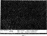
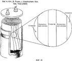
На фиг.1 показана полученная на сканирующем электронном микроскопе микрофотография (SEM) сверху вниз поверхности подложки из анодированного оксида алюминия (АОА), покрытой TaN путем атомно-слоевого осаждения и имеющей правильный шестиугольный массив пор диаметром ~ 30 нм,Figure 1 shows a scanning electron microscope (SEM) obtained from top to bottom of the surface of an anodized alumina (AOA) substrate coated with TaN by atomic layer deposition and having a regular hexagonal pore array with a diameter of ~ 30 nm,
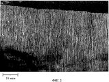
на фиг.2 - полученная на сканирующем электронном микроскопе микрофотография (SEM), иллюстрирующая местный поперечный разрез подложки из АОА с покрытием из TaN, выращенным путем атомно-слоевого осаждения (ALD, от английского - Atomic Layer Deposition),figure 2 is a scanning electron microscope micrograph (SEM) illustrating a local cross section of an AOA substrate with a TaN coating grown by atomic layer deposition (ALD, from the English - Atomic Layer Deposition),
на фиг.3 - изображение в общем виде пакета подложки из АОА и проводящей подложки, при этом подложка из АОА содержит массив цилиндрических отверстий согласно первому варианту осуществления настоящего изобретения,figure 3 is a General view of a package of a substrate of AOA and a conductive substrate, while the substrate of AOA contains an array of cylindrical holes according to the first embodiment of the present invention,
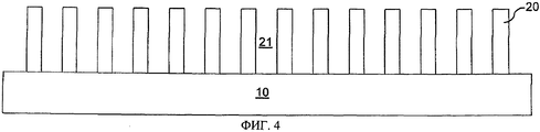
на фиг.4 - вертикальный вид в поперечном разрезе вдоль плоскости Z показанного на фиг.3 пакета подложки из АОА и проводящей подложки,figure 4 is a vertical view in cross section along the plane Z shown in figure 3 of the package of the substrate from AOA and conductive substrate,
на фиг.5 - вертикальный вид в поперечном разрезе пакета подложки из АОА и проводящей подложки после осаждения слоя псевдоемкостного материала согласно первому варианту осуществления настоящего изобретения,5 is a vertical cross-sectional view of an AOA substrate package and a conductive substrate after deposition of a layer of pseudo-capacitive material according to a first embodiment of the present invention,
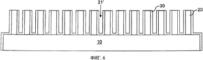
на фиг.6 - вертикальный вид в поперечном разрезе пакета подложки из АОА и проводящей подложки после удаления верхних участков слоя псевдоемкостного материала согласно первому варианту осуществления настоящего изобретения,FIG. 6 is a vertical cross-sectional view of an AOA substrate package and a conductive substrate after removing the upper portions of the pseudo-capacitive material layer according to the first embodiment of the present invention,
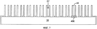
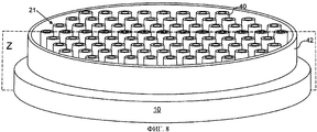
на фиг.7 - вертикальный вид в поперечном разрезе проводящей подложки и массива псевдоемкостных наноцилиндров после удаления подложки из АОА согласно первому варианту осуществления настоящего изобретения,7 is a vertical cross-sectional view of a conductive substrate and an array of pseudo-capacitive nanocylinders after removal of the substrate from AOA according to the first embodiment of the present invention,
на фиг.8 - изображение в общем виде показанной на фиг.7 проводящей подложки и массива псевдоемкостных наноцилиндров,on Fig - the image in General view shown in Fig.7 of the conductive substrate and the array of pseudo-capacitive nanocylinders,
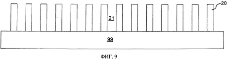
на фиг.9 - пакет подложки из АОА и съемной подложки, при этом подложка из АОА содержит массив цилиндрических отверстий согласно второму варианту осуществления настоящего изобретения,Fig.9 - a package of a substrate of AOA and a removable substrate, while the substrate of AOA contains an array of cylindrical holes according to the second embodiment of the present invention,
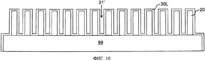
на фиг.10 - вертикальный вид в поперечном разрезе пакета подложки из АОА съемной подложки после осаждения слоя псевдоемкостного материала согласно второму варианту осуществления настоящего изобретения,10 is a vertical cross-sectional view of an AOA substrate package of a removable substrate after deposition of a layer of pseudo-capacitive material according to a second embodiment of the present invention,
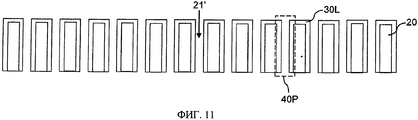
на фиг.11 - вертикальный вид в поперечном разрезе подложки из АОА и слоя псевдоемкостного материала после удаления съемной подложки согласно второму варианту осуществления настоящего изобретения,11 is a vertical cross-sectional view of a substrate of AOA and a layer of pseudo-capacitive material after removal of a removable substrate according to a second embodiment of the present invention,
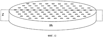
на фиг.12 - изображение в общем виде показанной на фиг.11 подложки из АОА и слоя псевдоемкостного материала,in Fig.12 - the image in General view shown in Fig.11 of the substrate of AOA and a layer of pseudo-capacitive material,
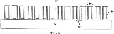
на фиг.13 - вертикальный вид в поперечном разрезе подложки из АОА и слоя псевдоемкостного материала после поворота на 180 градусов и помещения на проводящей подложке согласно второму варианту осуществления настоящего изобретения с необязательным на этой стадии прикреплением слоя псевдоемкостного материала к проводящей подложке,13 is a vertical cross-sectional view of an AOA substrate and a layer of pseudo-capacitive material after 180 degrees rotation and placement on a conductive substrate according to a second embodiment of the present invention with optionally attaching a layer of pseudo-capacitive material to the conductive substrate,
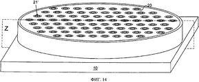
на фиг.14 - изображение в общем виде показанной на фиг.13 подложки из АОА, слоя псевдоемкостного материала и проводящей подложки,on Fig - the image in General view shown in Fig.13 of the substrate of AOA, a layer of pseudo-capacitive material and a conductive substrate,
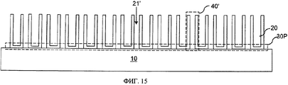
на фиг.15 - вертикальный вид в поперечном разрезе проводящей подложки и массива псевдоемкостных наноцилиндров после удаления подложки из АОА согласно второму варианту осуществления настоящего изобретения,15 is a vertical cross-sectional view of a conductive substrate and an array of pseudo-capacitive nanocylinders after removing the substrate from AOA according to a second embodiment of the present invention,
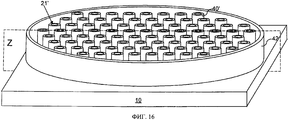
на фиг.16 - изображение в общем виде показанной на фиг.15 проводящей подложки и массива псевдоемкостных наноцилиндров, в котором все псевдоемкостные наноцилиндры связаны друг с другом листом из планарного слоя псевдоемкостного материала,in Fig.16 is a General view of the conductive substrate and an array of pseudocapacitive nanocylinders shown in Fig.15, in which all pseudocapacitant nanocylinders are connected to each other by a sheet of planar layer of pseudocapacitance material,
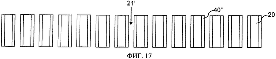
на фиг.17 - вертикальный вид в поперечном разрезе псевдоемкостных наноцилиндров и подложки из АОА после удаления верхних участков слоя псевдоемкостного материала, показанного на фиг.11, согласно третьему варианту осуществления настоящего изобретения,on Fig is a vertical cross-sectional view of the pseudo-capacitive nanocylinders and the substrate from AOA after removing the upper sections of the layer of pseudo-capacitive material shown in Fig. 11, according to a third embodiment of the present invention,
на фиг.18 - изображение в общем виде проводящей подложки и массива псевдоемкостных наноцилиндров, показанной на фиг.17,on Fig is a General view of a conductive substrate and an array of pseudo-capacitive nanocylinders shown in Fig.17,
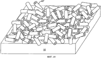
на фиг.19 - изображение в общем виде произвольного пакета псевдоемкостных наноцилиндров на проводящей подложке, полученных путем удаления показанной на фиг.18 подложки из АОА и осаждения псевдоемкостных наноцилиндров на проводящую подложку,on Fig - a General view of an arbitrary package of pseudo-capacitive nanocylinders on a conductive substrate, obtained by removing the substrate shown in Fig.18 from AOA and deposition of pseudo-capacitive nanocylinders on a conductive substrate,
на фиг.20 - схематический вид накопителя энергии с использованием псевдоемкостных наноцилиндров.on Fig is a schematic view of an energy storage device using pseudo-capacitive nanocylinders.
Осуществление изобретенияThe implementation of the invention
Как указано выше, настоящее изобретение относится к накопителю энергии, содержащему по меньшей мере один наноструктурный электрод с большой площадью поверхности псевдоемкостного материала для псевдоемкостного накопления энергии, и способам его изготовления, которые будут подробно описаны со ссылкой на сопровождающие чертежи. Следует отметить, что одинаковые элементы в различных вариантах осуществлении обозначены на чертежах одинаковыми позициями.As indicated above, the present invention relates to an energy storage device comprising at least one nanostructured electrode with a large surface area of a pseudo-capacitive material for pseudo-capacitive energy storage, and methods for its manufacture, which will be described in detail with reference to the accompanying drawings. It should be noted that the same elements in various embodiments are indicated by the same reference numbers in the drawings.
Рассмотрим на фиг.1, на которой показана полученная на сканирующем электронном микроскопе микрофотография (SEM) сверху вниз поверхности подложки из анодированного оксида алюминия (АОА) с правильным шестиугольным массивом пор диаметром ~ 60 нм. Из техники известно, что под действием кислотных электролитов для анодирования в анодированном покрытии из алюминия образуются поры. Примеры кислот, которые могут использоваться для анодирования алюминия, включают без ограничения фосфорную кислоту и серную кислоту. Размер и шаг пор зависят от типа осуществляемого анодирования, температуры анодирования и напряжения формовки. Поры могут иметь диаметр примерно от 10 до 200 нм, а толщина стенок (расстояние между соседними порами) может составлять от 10 до 200 нм, хотя при соответствующих условиях анодирования могут быть получены меньшие и большие диаметры и толщины стенок. Длина пор может быть на несколько порядков величины больше их диаметра и может превышать диаметр примерно до 25000 раз.We consider in FIG. 1, which shows a scanning electron microscope (SEM) obtained from top to bottom of the surface of an anodized alumina (AOA) substrate with a regular hexagonal pore array with a diameter of ~ 60 nm. It is known from the art that under the influence of acid electrolytes for anodizing, pores are formed in the anodized coating of aluminum. Examples of acids that can be used to anodize aluminum include, but are not limited to, phosphoric acid and sulfuric acid. The size and pitch of the pores depend on the type of anodizing performed, the anodizing temperature and the molding voltage. The pores can have a diameter of about 10 to 200 nm, and the wall thickness (distance between adjacent pores) can be from 10 to 200 nm, although smaller and larger diameters and wall thicknesses can be obtained under appropriate anodizing conditions. The length of the pores can be several orders of magnitude greater than their diameter and can exceed the diameter of up to about 25,000 times.
Рассмотрим на фиг.2, на которой показана полученная на сканирующем электронном микроскопе микрофотография (SEM), иллюстрирующая местный поперечный разрез подложки из АОА, имеющей покрытие из слоя TaN, выращенного путем атомно-слоевого осаждения (ALD). Слой TaN предотвращает накопление зарядов и/или образование дуги в изоляционном материале подложки из АОА. Вертикальные цилиндрические поры проходят по всему поперечному сечению подложки из АОА, а соотношение размеров, т.е. соотношение длины поры и диаметра поры может достигать 25000 или более, как указано выше.Refer to FIG. 2, which shows a scanning electron microscope (SEM) photograph showing a local cross section of an AOA substrate coated with a TaN layer grown by atomic layer deposition (ALD). The TaN layer prevents the accumulation of charges and / or arcing in the insulation material of the AOA substrate. Vertical cylindrical pores extend over the entire cross-section of the AOA substrate, and the aspect ratio, i.e. the ratio of pore length to pore diameter can reach 25,000 or more, as described above.
Рассмотрим фиг.3 и 4, на которых показан первый пример структуры согласно первому варианту осуществления настоящего изобретения, а именно изображение в общем виде на фиг.3 и вертикальный вид в поперечном разрезе на фиг.4. Плоскость Z на фиг.3 является вертикальной плоскостью поперечного сечения на фиг.4.Refer to FIGS. 3 and 4, which show a first example of a structure according to a first embodiment of the present invention, namely, a general view of FIG. 3 and a vertical cross-sectional view of FIG. 4. The plane Z in figure 3 is a vertical plane of the cross section in figure 4.
Структура согласно первому примеру содержит пакет проводящей подложки 10 и подложки 20 из анодированного оксида алюминия (АОА). Подложка 20 из АОА представляет собой лист алюминиевой фольги, анодированной с целью преобразования в слой оксида алюминия, который содержит самособранный массив вертикальных пор. Подложка 20 из АОА может быть сформирована известными из техники способами. Подложка 20 из АОА содержит массив "нанопор" 21, то есть пор диаметром менее 1 мкм. Диаметр отдельных нанопор 21 и шаг массива нанопор 21 могут регулироваться путем изменения параметров анодирования.The structure according to the first example comprises a stack of
Обычно диаметр каждой нанопоры 21 составляет от 10 до 200 нм, хотя могут быть возможны меньшие и большие диаметры в зависимости от оптимизации условий процесса в будущем. Толщина подложки 20 из АОА по меньшей мере в 50 раз превышает диаметр нанопор 21 и может до превышать диаметр нанопор 21 в 25000 или более раз. Обычно толщина подложка 20 из АОА составляет от 10 мкм до 5 мм, хотя могут использоваться меньшие и большие толщины. Каждая нанопора 21 представляет собой цилиндрическое отверстие, проходящее от самой верхней планарной поверхности подложка 20 из АОА до самой нижней поверхности подложки 20 из АОА, которая соприкасается с самой верхней планарной поверхностью проводящей подложки 10. Таким образом, в подложке 20 из АОА содержится множество отверстий, которые представляют собой множество нанопор 21. Множество отверстий могут образовывать двумерный периодический массив, такой как шестиугольный массив.Typically, the diameter of each
Подложка 20 из АОА помещена на проводящую подложку 10, которая содержит проводящий материал, такой как элементарный металл, интерметаллический сплав по меньшей мере двух элементарных металлов, проводящий оксид металла, проводящий нитрид металла, сильнолегированный полупроводниковый материал или их сплав или пакет. Материал проводящей подложки выбирают таким образом, чтобы он без потери структурной целостности выдерживал травление, которое затем осуществляют, чтобы удалить подложку 20 из АОА. Толщина подложка 20 из АОА может составлять от 50 мкм до 1 мм, хотя могут использоваться меньшие и большие толщины. Самая нижняя поверхность подложки 20 из АОА соприкасается с самой верхней планарной поверхностью проводящей подложки 10. Хотя подложка 20 из АОА и проводящая подложка 10 имеют планарную в микроскопическом масштабе границу раздела, конструкция, образованная подложкой 20 из АОА и проводящей подложкой 10, при необходимости может быть согнута в макроскопическом масштабе. Проводящая подложка 10 предпочтительно представляет собой тонкую легкую подложку для доведения до максимума плотности накапливаемой энергии на общую массу накопителя энергии.
На фиг.5 показан пакет подложки из АОА и проводящей подложки после конформного осаждения слоя 30L псевдоемкостного материала согласно первому варианту осуществления настоящего изобретения. Используемый в описании термин "псевдоемкостный материал" означает материал, который способен накапливать энергию посредством обратимой реакции восстановления-окисления на его поверхности. Псевдоемкостные материалы включают некоторые металлы и оксиды некоторых металлов. Феномен накопления и высвобождения энергии псевдоемкостным материалом посредством реакции восстановления-окисления именуется "псевдоемкостью". Псевдоемкостные материалы включают без ограничения оксид марганца (MnO2), оксид рутения (RuO2), оксид никеля (NiO) и их сочетание.5 shows a package of a substrate of AOA and a conductive substrate after conformal deposition of the
Обычно исключительно высокое соотношение размеров нанопор 21 (по меньшей мере 50) делает необходимым использование атомно-слоевого осаждения (ALD) с целью получения конформного покрытия из псевдоемкостного материала на боковых стенках нанопор 21 в подложке из АОА 10. Подложка 20 из АОА действует как матрица для осаждения слоя 30L псевдоемкостного материала.Typically, the exceptionally high nanopore size ratio of 21 (at least 50) makes it necessary to use atomic layer deposition (ALD) to obtain a conformal coating of pseudocapacitious material on the side walls of
При атомно-слоевом осаждении осаждают монослой первого материала в ходе самоограничивающейся реакции, которая достигает состояния насыщения после формирования монослоя первого материала в результате подачи первого реагента в камеру для осаждения. После удаления первого реагента, осаждают монослой второго материала в ходе другой самоограничивающейся реакции, которая достигает состояния насыщения после формирования монослоя второго материала в результате подачи второго реагента в камеру для осаждения. Первый реагент и второй реагент попеременно подают в одну и ту же камеру для осаждения с определенной длительностью нагнетания между каждым циклом осаждения монослоя. В случае псевдоемкостного материала в виде оксида металла осаждают предшественник металла в ходе самоограничивающейся реакции, которая достигает состояния насыщения после формирования монослоя атомов металла в результате подачи металлосодержащего реагента в камеру для осаждения. После удаления металлосодержащего реагента осаждают монослой кислорода в ходе самоограничивающейся реакции, которая достигает состояния насыщения после формирования монослоя атомов кислорода в результате подачи газообразного кислорода в камеру для осаждения. Затем откачивают кислород из камеры для осаждения. Стадии подачи металлосодержащего реагента, нагнетания металлосодержащего реагента, подачи газообразного кислорода и нагнетания газообразного кислорода многократно повторяют циклически с целью осаждения слоя оксида металла с характеристиками псевдоемкости, т.е. "псевдоемкостного" слоя оксида металла. Слой 30L псевдоемкостного материала осаждают на обнаженные поверхности проводящей подложки 10 на дне каждой нанопоры 21.In atomic-layer deposition, a monolayer of the first material is deposited during a self-limiting reaction, which reaches a saturation state after the formation of a monolayer of the first material by feeding the first reagent to the deposition chamber. After removal of the first reagent, a monolayer of the second material is precipitated during another self-limiting reaction, which reaches a saturation state after the monolayer of the second material is formed by feeding the second reagent to the deposition chamber. The first reagent and the second reagent are alternately fed into the same deposition chamber with a certain injection duration between each deposition cycle of the monolayer. In the case of a pseudocapacitious material, a metal precursor is precipitated in the form of a metal oxide in the course of a self-limiting reaction, which reaches a saturation state after the formation of a monolayer of metal atoms by supplying a metal-containing reagent to the deposition chamber. After removal of the metal-containing reagent, an oxygen monolayer is precipitated during a self-limiting reaction, which reaches a saturation state after the formation of a monolayer of oxygen atoms by supplying gaseous oxygen to the deposition chamber. Then oxygen is pumped out from the deposition chamber. The steps of supplying a metal-containing reagent, injecting a metal-containing reagent, supplying gaseous oxygen and injecting gaseous oxygen are repeatedly repeated cyclically in order to deposit a metal oxide layer with pseudo-capacitance characteristics, i.e. "pseudocapacitance" layer of metal oxide. The
Толщина слоя 30L псевдоемкостного материала может точно регулироваться с точностью до атомарного уровня. Кроме того, толщина слоя 30L псевдоемкостного материала является одинаковой на протяжении всего слоя 30L псевдоемкостного материала с атомарной точностью за счет самоограничивающей природы реакций в процессе ALD. Толщину слоя 30L псевдоемкостного материала выбирают таким образом, чтобы она составляла менее половины диаметра нанопор 21, в результат чего на каждом углубленном участке слоя 30L псевдоемкостного материала образуется полость 21' меньшего диаметра, чем диаметр нанопор 21. На этой стадии весь слой 30L псевдоемкостного материала является непрерывным. По существу, внутренний диаметр нанотрубки может тонко регулироваться вплоть до 1 нанометра и менее, и при таком диаметре наблюдается существенное увеличение емкости. Смотри, например, J.Chmiola, G.Yushin, Y.Gogotsi, C.Portet, P.Simon и Р.L.Taberna, "Anomalous increase in carbon capacitance at pore sizes less than 1 nanometer" Science 313, 1760 (2006).The thickness of the
Обычно атомно-слоевое осаждение необходимо для достижения требуемого высокого уровня конформности и общего геометрического регулирования для формирования непрерывного слоя 30L псевдоемкостного материала, который доходит до дна нанопор 21. Попытки применения электроосаждения сталкиваются с двумя сложностями. Первая сложность состоит в том, что подложка 20 из АОА неприменима в качестве электрода для электроосаждения, поскольку подложка 20 из АОА является изолятором. Для применения электроосаждения обнаженные поверхности подложки 20 из АОА должны быть преобразованы в проводящую поверхность путем формирования сначала равномерного покрытия проводящего материала. Таким образом, атомно-слоевое осаждение в любом случае необходимо даже для формирования проводящего затравочного слоя в целях применения электроосаждения. Вторая сложность состоит в том, что диаметры нанопор 21 слишком малы, а соотношение размеров нанопор 21 слишком велико для применения электроосаждения даже в случае успешного создания проводящего затравочного слоя. Электролитические жидкости и электрические поля не способны проникать до нижнего участка нанопор 21 из-за малых диаметров нанопор 21 и большого соотношение размеров (по меньшей мере 10, обычно более 50) нанопор 21, что делает электроосаждение неосуществимым.Typically, atomic layer deposition is necessary to achieve the required high level of conformity and overall geometric control to form a
Химическое осаждение из паровой фазы (CVD) является общим процессом в газовой фазе, в ходе которого происходит крекинг предшественника на нагретой поверхности. Хотя способ химического осаждения из паровой фазы является в принципе применимым, химическое осаждение из паровой фазы не обеспечивает тонкой регулировки толщины, которую обеспечивает атомно-слоевое осаждение. В настоящее время не существует процесса химического осаждения из паровой фазы, позволяющего надежно достигать дна нанопор 21 с учетом малого диаметра нанопор 21 и большого соотношения размеров каждой нанопоры 21. В настоящее время атомно-слоевое осаждение является практически единственным осуществимым способом формирования конформного слоя псевдоемкостного материала, который соприкасается с самыми нижними участками нанопор 21. Использование атомно-слоевое осаждение позволяет покрывать боковые стенки нанопор 21 и формировать единый непрерывный слой 30L псевдоемкостного материала с учетом длины, диаметра и шага массива нанопор 21. Толщина слоя 30L псевдоемкостного материала может составлять от 1 нм до 75 нм, обычно от 3 нм до 30 нм, хотя могут использоваться меньшие и большие толщины.Chemical vapor deposition (CVD) is a common process in the gas phase during which the precursor is cracked on a heated surface. Although the chemical vapor deposition method is in principle applicable, chemical vapor deposition does not provide fine adjustment of the thickness provided by atomic layer deposition. At present, there is no process of chemical vapor deposition that can reliably reach the bottom of
Как показано на фиг.6, верхние поверхности подложки 20 из АОА обнажают путем удаления дистальных планарных участков слоя 21 псевдоемкостного материала. Дистальные участки слоя 21 псевдоемкостного материала означают непрерывные планарные участки слоя 21 псевдоемкостного материала, расположенные на и над самыми верхними поверхностями подложки 20 из АОА. Дистальные участки слоя 30L псевдоемкостного материала могут быть удалены, например, путем химической механической планаризации или анизотропного травления, такого как травления химически активными ионами. В случае применения химической механической планаризации дистальные участки слоя 30L псевдоемкостного материала могут быть удалены путем шлифования, в ходе которого по мере необходимости используют химическую суспензию. В случае применения анизотропного травления травители в газовой фазе с определенной направленностью, т.е. по вертикали сталкиваются с дистальными участками слоя 30L псевдоемкостного материала. Обычно травителями не травят самые нижние участки слоя 30L псевдоемкостного материала, которые контактируют с проводящей подложкой 10 внутри полостей 21' за счет большого соотношения размеров полостей 21', которое превосходит соотношение размеров незаполненных нанопор 21 (смотри фиг.4.)As shown in FIG. 6, the upper surfaces of the
Как показано на фиг.7 и 8, путем удаления подложки 20 из АОА образуется множество псевдоемкостных "наноцилиндров" 40. Используемый в описании термин "наноцилиндр" означает структуру, содержащую цилиндрическую трубку, наружный диаметр которой не превышает 1 мкм. Обычно наружный диаметр наноцилиндров составляет от 10 нм до 200 нм, хотя также могут использоваться меньшие и большие наружные диаметры (менее 1 мкм). Оксид алюминия в подложке из АОА может быть подвергнут травлению любым способом, например с использованием стандартных способов влажного травления, таких как погружение в водную хромовую кислоту. В результате формируется множество псевдоемкостных наноцилиндров 40 в виде массива псевдоемкостных наноцилиндров 40, представляющих собой нанотрубки из структурно устойчивых псевдоемкостных материалов. Иными словами, из участков слоя 30L псевдоемкостного материала, остающихся после удаления подложки 20 из АОА, образуется множество псевдоемкостных наноцилиндров 40. До удаления подложки 20 из АОА она действует как несущий каркас двумерного периодического массива псевдоемкостных наноцилиндров 40. После удаления подложки 20 из АОА остается только конструкция, образованная проводящей подложкой 10, массивом псевдоемкостных наноцилиндров 40 и наружной псевдоемкостной стенкой 42.As shown in FIGS. 7 and 8, by removing the
Удаление подложки 20 из АОА обеспечивает многообразные преимущества. Во-первых, за счет удаления подложки 20 из АОА формируется двумерный упорядоченный массив псевдоемкостных наноцилиндров 40, который может использоваться в составе электрода с исключительно большой удельной площадью поверхности. "Удельная площадь поверхности" означает площадь поверхности на единицу массы. Например, двумерный упорядоченный массив псевдоемкостных наноцилиндров 40 может иметь поверхностную плотность до 1016/м2 и удельную площадь поверхности около 500 м2/г. Удельная площадь поверхности может быть в два-три раза большей в зависимости от конкретного строения боковых стенок псевдоемкостных наноцилиндров 40, например если поверхностям псевдоемкостных наноцилиндров 40 придана шероховатость или текстура.Removing
Во-вторых, за счет удаления подложки 20 из АОА уменьшается общая масса структуры согласно первому примеру вследствие уменьшения паразитной массы, т.е. общей массы материалов, которая не способствует накоплению зарядов. Иными словами, за счет полного удаления всех материалов, которые не способствуют накоплению энергии, т.е. оксида алюминия, в подложке 20 из АОА увеличивается удельная энергия по массе структуры согласно первому примеру. На этой стадии конструкция 10, 40, 42 с уменьшенной массой, в которую входят все остающиеся участки структуры согласно первому примеру, может впоследствии выгодно использоваться для создания легкого электрода, содержащего конструкцию, образованную проводящей подложкой 10 и массивом псевдоемкостных наноцилиндров 40.Secondly, due to the removal of the
В-третьих, за счет удаления подложки 20 из АОА более чем вдвое увеличивается общая площадь поверхности псевдоемкостного материала и тем самым вдвое увеличивается удельная емкость, т.е. емкость на единицу массы. Поскольку за счет обнаженных наружных поверхностей боковых стенок участков псевдоемкостных наноцилиндров 40 увеличивается общая площадь поверхности, соответствующим образом увеличивается общая емкость конструкции 10, 40, 42. Когда конструкция 10, 40, 42 действует как электрод, верхний участок 40, 42 электрода полностью оптимизирован для накопления электрических зарядов посредством фарадеевских процессов, т.е. процессов переноса зарядов, в которых используется окисление и восстановление. В этом случае проводящая подложка 10 действует как участок электрода, на котором конструктивно крепится массив псевдоемкостных наноцилиндров 40.Thirdly, due to the removal of the
Таким образом, в электроде может использоваться множество псевдоемкостных наноцилиндров 40, расположенных на проводящей подложке 10. Каждый псевдоемкостный наноцилиндр 40 содержит псевдоемкостный материал и имеет выполненную в нем внутреннюю полость 21'. Псевдоемкостный наноцилиндр 40 не образует оболочку вокруг полости 21', а имеет отверстие на одном конце. Отверстие на одном конце сообщается с полостью 21' в каждом псевдоемкостном наноцилиндре 40.Thus, a plurality of
Каждый псевдоемкостный наноцилиндр 40 имеет торцевую крышку 40Е без отверстия в ней на конце, противоположном концу с отверстием, сообщающимся с полостью 21'. Все псевдоемкостные наноцилиндры 40 имеют равномерную (одинаковую) толщину на всем протяжении, включая торцевую крышку 40Е, которая имеет наружную торцевую поверхность. Наружная торцевая поверхность каждого псевдоемкостного наноцилиндра 40 примыкает к боковым стенкам этого псевдоемкостного наноцилиндра 40 по всей его окружности. Кроме того, вся торцевая поверхность каждого псевдоемкостного наноцилиндра 40 соприкасается с проводящей подложкой 10 и прикреплена к ней.Each
Множество псевдоемкостных наноцилиндров 40 образуют массив псевдоемкостных наноцилиндров 40, боковые стенки которых перпендикулярны верхней поверхности проводящей подложки 10. Каждый псевдоемкостный наноцилиндр 40 не соприкасается с каким-либо другим псевдоемкостным наноцилиндром 40, т.е. разъединен с другими псевдоемкостными наноцилиндрами 40. Таким образом, каждый псевдоемкостный наноцилиндр 40 отстоит в боковом направлении от любого другого из множества емкостных наноцилиндров 40.The plurality of
На наружные боковые стенки и/или внутренние боковые стенки множества псевдоемкостных наноцилиндров 40 необязательно может быть нанесено покрытие из функциональных молекулярных групп. Функциональные группы содержат дополнительный псевдоемкостный материал, который способен увеличивать накопление зарядов множеством псевдоемкостных наноцилиндров 40. Примеры функциональных групп включают без ограничения полианилин, являющийся проводящим полимером. Покрытие из функциональных групп может наноситься в ходе по меньшей мере другого процесса или процессов атомно-слоевого осаждения с использованием осаждения из паровой фазы или мокрого химического осаждения. Покрытия на внутренние боковые стенки и наружные боковые стенки могут наноситься на одной стадии или на нескольких стадиях. Например, покрытие на внутренние и наружные боковые стенки может наноситься после удаления подложки 20 из АОА. В качестве альтернативы, покрытие на внутренние боковые стенки множества псевдоемкостных наноцилиндров 40 может наноситься до удаления подложки 20 из АОА, а покрытие на наружные боковые стенки наноцилиндров 40 может наноситься после удаления подложки 20 из АОА. Для нанесения покрытия на наружные боковые стенки и/или внутренние боковые стенки множества псевдоемкостных наноцилиндров 40 могут использоваться известные из техники материалы и способы. Смотри, например, Stewart, M.P.; Maya, F.; Kosynkin, D.V.; Dirk, S.M.; Stapleton, J.J.; McGuiness, C.L.; Allara, D.L; Tour, J.M. "Direct Covalent Grafting of Conjugated Molecules onto Si, GaAs, and Pd Surfaces from Aryldiazonium Salts," J. Am. Chem Soc. 2004, 126, 370-378.Outer side walls and / or inner side walls of the plurality of
На фиг.9 проиллюстрирован второй пример структуры согласно второму варианту осуществления настоящего изобретения, которая содержит пакет подложки 20 из АОА и съемной подложки 99. Подложка 20 из АОА может быть такой же, как и в первом варианте осуществления. Съемная подложка 99 может содержать проводящий материал, полупроводниковый материал, изолирующий материал или их сочетание. Материал съемной подложки 99 выбирают с целью его легкого удаления избирательно по отношению к материалу подложки 20 из АОА, т.е. без удаления материала подложка 20 из АОА способом, который будет описан далее. Удаление съемной подложки 99 может осуществляться механическим способом, химико-механическим способом или химическим способом. Толщина съемной подложки 99 может составлять от 10 до 500 мкм, хотя могут использоваться меньшие и большие толщины.Fig. 9 illustrates a second example of a structure according to a second embodiment of the present invention, which comprises a package of a
Как показано на фиг.10, на пакет подложки 20 из АОА и съемной подложки 99 осаждают слой 30L псевдоемкостного материала. Осаждение слоя 30L псевдоемкостного материала может осуществляться таким же способом, что и в первом варианте осуществления, т.е. путем атомно-слоевого осаждения. Участки слоя 30L псевдоемкостного материала на дне каждой полости 21' соприкасаются с верхней поверхностью съемной подложки 99.As shown in FIG. 10, a
Как показано на фиг.11 и 12, съемную подложку 99 и нижние участки слоя 30L псевдоемкостного материала удаляют, чтобы сформировать конструкцию, образованную подложкой 20 из АОА и остающимися участками слоя 30L псевдоемкостного материала. Удаление съемной подложки 99 может осуществляться избирательно по отношению к конструкции, образованной подложкой 20 из АОА и слоем 30L псевдоемкостного материала, например способом механического удаления, такого как стачивание, химико-механического удаления, такого как химическая механическая планаризация, химического удаления, такого как влажное травление или сухое травление, или с использованием их сочетания. После удаления съемной подложки 99 обнажаются самые нижние поверхности слоя 30L псевдоемкостного материала, которые являются теми же, что и наружные торцевые поверхности торцевых крышек 40Е на фиг.7, и самые нижние поверхности подложки из АОА.As shown in FIGS. 11 and 12, the
Затем способом неизбирательного удаления, таким как стачивание или химическая механическая планаризация, или неизбирательного травления удаляют самые нижние участки подложки 20 из АОА и самые нижние горизонтальные участки слоя 30L псевдоемкостного материала, которые соответствуют торцевым крышкам 40Е на фиг.7. После удаления самых нижних горизонтальных участков слоя 30L псевдоемкостного материала каждая полость 21' проходит от самой верхней поверхности конструкции 20, 30L, образованной подложкой 20 из АОА и слоем 30L псевдоемкостного материала, до самой нижней поверхности конструкции 20, 30L и имеет отверстие сверху и другое отверстие на дне. Участок слоя 30L псевдоемкостного материала вокруг каждой полости 21' образует прототипический псевдоемкостный наноцилиндр 40Р. Весь слой 30L псевдоемкостного материала является непрерывным, поскольку каждый прототипический псевдоемкостный наноцилиндр 40Р сообщается со всеми другими прототипическими псевдоемкостными наноцилиндрами 40Р посредством верхних горизонтальных участков слоя 30L псевдоемкостного материала, расположенных между каждой соседней парой прототипических псевдоемкостных наноцилиндров 40Р.Then, by the method of non-selective removal, such as grinding or chemical mechanical planarization, or non-selective etching, the lowermost portions of the
Как показано на фиг.13 и 14, конструкция 20, 30L, образованная подложкой 20 из АОА и слоем 30L псевдоемкостного материала, повернута на 180 градусов. Конструкция 20, 30L необязательно может помещаться на проводящую подложку 10, которая может иметь такой же состав и толщину, что и проводящая подложка 10 из первого варианта осуществления. В случае применения проводящей подложки 10 на этой стадии слой 30L псевдоемкостного материала может быть необязательно прикреплен к проводящей подложке 10. В одном из вариантов осуществления нижние поверхности слоя 30L псевдоемкостного материала постоянно прикреплены, например, с использованием проводящего клеящего вещества (не показано). В другом варианте осуществления конструкция 20, 30L, образованная подложкой 20 из АОА и слоем 30L псевдоемкостного материала, не прикреплена или временно прикреплена к проводящей подложке 10 с возможностью последующего отсоединения слоя 30L псевдоемкостного материала.As shown in FIGS. 13 and 14, the
Как показано на фиг.15 и 16, подложку 20 из АОА удаляют тем же способом, как и в первом варианте осуществления, проиллюстрированном на фиг.7 и 8. В случае применения проводящей подложки 10 планарный слой 30Р псевдоемкостного материала соприкасается с верхней поверхностью проводящей подложки 10. После удаления подложки 20 из АОА наружные боковые стенки прототипических псевдоемкостных наноцилиндров 40Р обнажаются, и множество прототипических псевдоемкостных наноцилиндров 40Р становятся множеством псевдоемкостных наноцилиндров 40'. Все псевдоемкостные наноцилиндры 40' связаны друг с другом посредством листа из планарного слоя 30Р псевдоемкостного материала.As shown in FIGS. 15 and 16, the
Остающиеся участки слоя 30Р псевдоемкостного материала содержат множество псевдоемкостных наноцилиндров 40' и планарный слой 30Р псевдоемкостного материала, которые имеют цельную конструкцию и одинаковую толщину и состав на всем протяжении. Таким образом, все емкостные наноцилиндры 40' указанного множества связаны друг с другом посредством планарного слоя 30Р псевдоемкостного материала на дне каждого из емкостных наноцилиндров 40'. В планарном слое 30Р псевдоемкостного материала имеется по меньшей мере такое же число отверстий, что и общее число псевдоемкостных наноцилиндров 40' из множества псевдоемкостных наноцилиндров 40'. Из множества псевдоемкостных наноцилиндров 40' формируется массив псевдоемкостных наноцилиндров, имеющий такую же двумерную периодичность, что и нанопоры в подложке 20 из АОА (которая уже отсутствует на этой стадии, смотри фиг.9). Если присутствует проводящая подложка 10, массив псевдоемкостных наноцилиндров 40' имеет вертикальные боковые стенки, перпендикулярные верхней поверхности проводящей подложки 10.The remaining portions of the
Каждый псевдоемкостный наноцилиндр 40' содержит псевдоемкостный материал и имеет выполненную в нем внутреннюю полость 21'. Полость 21' в каждом псевдоемкостном наноцилиндре 40' не заключена в оболочку из этого псевдоемкостного наноцилиндра 40'. Каждый псевдоемкостный наноцилиндр 40' имеет две торцевые поверхности, в каждой из которых имеется отверстие. Каждый псевдоемкостный наноцилиндр 40' имеет два отверстия, которые расположены на концах этого псевдоемкостного наноцилиндра 40'. В частности, каждый псевдоемкостный наноцилиндр 40' имеет отверстие в верхнем конце, т.е. верхнее отверстие и другое отверстие в нижнем конце, т.е. нижнее отверстие. Каждое из отверстий, включающих верхнее отверстие и нижнее отверстие, сообщается с полостью 21. Верхнее отверстие сообщается с окружающей средой. Нижнее отверстие также может сообщаться с окружающей средой, если не используется проводящая подложка 10, или может быть закрыто верхней поверхностью проводящей подложки 10, если используется проводящая подложка 10. В случае присутствия проводящей подложки 10 боковые стенки множества псевдоемкостных наноцилиндров 40' перпендикулярны верхней поверхности проводящей подложки 10.Each pseudo-capacitive nanocylinder 40 'contains a pseudo-capacitive material and has an internal cavity 21' formed therein. The cavity 21 'in each pseudo-capacitive nanocylinder 40' is not enclosed in a shell of this pseudo-capacitive nanocylinder 40 '. Each pseudo-capacitive nanocylinder 40 'has two end surfaces, each of which has an opening. Each pseudo-capacitive nanocylinder 40 'has two openings that are located at the ends of this pseudo-capacitive nanocylinder 40'. In particular, each pseudo-capacitive nanocylinder 40 'has an opening at its upper end, i.e. the upper hole and another hole in the lower end, i.e. bottom hole. Each of the holes, including the upper hole and the lower hole, communicates with the
Структура согласно второму примеру может использоваться в качестве электрода накопителя энергии. В одном из вариантов осуществления электрод содержит множество псевдоемкостных наноцилиндров 40', планарный слой 30Р псевдоемкостного материала и проводящую подложку 10. В другом варианте осуществления электрод содержит множество псевдоемкостных наноцилиндров 40' и планарный слой 30Р псевдоемкостного материала, но не содержит проводящую подложку 10. Такими же способами, как и в первом варианте осуществления, необязательно может наноситься покрытие из соответствующих функциональных групп.The structure according to the second example can be used as an energy storage electrode. In one embodiment, the electrode comprises a plurality of pseudocapacitant nanocylinders 40 ', a
Как показано на фиг.17, в третьем варианте осуществления настоящего изобретения структура согласно третьему примеру может быть получена из проиллюстрированной на фиг.11 и 12 структуры согласно второму примеру путем удаления самого верхнего планарного участка слоя 30L псевдоемкостного материала с целью обнажения поверхностей подложка 20 из АОА. В качестве альтернативы, структура согласно третьему примеру может быть получена из проиллюстрированной на фиг.10 структуры согласно второму примеру путем сначала удаления самого верхнего планарного участка слоя 30L псевдоемкостного материала с целью обнажения поверхностей подложка 20 из АОА, а затем удаления съемной подложки 99 и нижних участков слоя 30L псевдоемкостного материала. В результате формируется конструкция 20, 40'', образованная подложкой 20 из АОА и множеством псевдоемкостных наноцилиндров 40''. Каждый псевдоемкостный наноцилиндр 40'' представляет собой цилиндрическую трубку, которая является топологически гомеоморфной тору и имеет обнаженную внутреннюю вертикальную боковую стенку, обнаженную верхнюю торцевую поверхность с отверстием в ней и обнаженную нижнюю торцевую поверхность с отверстием в ней. Наружная вертикальная боковая стенка каждого псевдоемкостного наноцилиндра 40'' соприкасается с подложкой 20 из АОА, которая на этой стадии удерживает на месте множество псевдоемкостных наноцилиндров 40''. Поверхности подложки из АОА 10 обнажены сверху и снизу.As shown in FIG. 17, in a third embodiment of the present invention, the structure according to the third example can be obtained from the structure illustrated in FIGS. 11 and 12 by removing the uppermost planar portion of the
Как показано на фиг.19, конструкция 20, 40'', образованная подложкой 20 из АОА и множеством псевдоемкостных наноцилиндров 40'', помещена на проводящую подложку 10 или временную подложку (не показана), при этом подложку 20 из АОА удаляют таким же способом, как и в первом варианте осуществления, проиллюстрированном на фиг.7 и 8. После стравливания подложки 20 из АОА все псевдоемкостные наноцилиндры 40'' отсоединяются друг от друга и падают на проводящую подложку 10 или временную подложку.As shown in FIG. 19, the
При падении псевдоемкостных наноцилиндров 40'' их ориентация становится "рандомизированной", т.е. случайной. Используемый в описании термин "случайная" ориентация или "рандомизированная" ориентация означает несоосность элементов и геометрии, которые включают ближний порядок или случайную тенденцию дальнего порядка. Например, ориентация псевдоемкостных наноцилиндров 40'' считается "случайной" даже в случае более высокой вероятности какой-либо конкретной ориентации, например, вследствие наклона проводящей подложки 10 или временной подложки во время травления, чтобы вызвать падение с предпочтительной ориентацией, поскольку процесс падения по своей природе вносит неопределенность в окончательную ориентацию каждого из псевдоемкостных наноцилиндров 40''.When the pseudo-capacitive nanocylinders 40 '' fall, their orientation becomes "randomized", i.e. random. Used in the description, the term "random" orientation or "randomized" orientation means misalignment of elements and geometry, which include short-range order or random long-range order. For example, the orientation of the
Множество псевдоемкостных наноцилиндров 40'' могут быть прикреплены к проводящей подложке 10, например, с использованием тонкого слоя проводящего клеящего вещества. В случае использования временной подложки множество псевдоемкостных наноцилиндров 40'' может быть размещено на проводящей подложке 10, покрытой тонким слоем проводящего клеящего вещества, в результате чего множество псевдоемкостных наноцилиндров 40'' прикрепляется к проводящей подложке. Ориентация множества псевдоемкостных наноцилиндров 40'' после размещения на проводящей подложке 10 в результате падения непосредственно на проводящую подложку 10 или падения на временную подложку и затем помещения на проводящую подложку 10 является рандомизированной.Many
Каждый псевдоемкостный наноцилиндр 40'' содержит псевдоемкостный материал и имеет выполненную в нем полость 21'. Каждый псевдоемкостный наноцилиндр 40'' имеет два отверстия, которые расположены на его концах. Каждое отверстие выполнено в торцевой поверхности псевдоемкостного наноцилиндра 40''. Каждое отверстие сообщается с полостью 21'. Таким образом, полость 21' в каждом псевдоемкостном наноцилиндре 40'' не заключена в оболочку из такого псевдоемкостного наноцилиндра 40''.Each
Структура согласно третьему примеру может использоваться в качестве электрода накопителя энергии. В этом случае электродом является "электрод из рандомизированных наноцилиндров", у которого ориентация псевдоемкостного наноцилиндра 40'' является рандомизированной в двумерной плоскости, параллельной локальному участку проводящей подложки 10. Электрод может быть согнут по мере необходимости вместе с находящимся внутри псевдоемкостным наноцилиндром 40''. Такими же способами, как и в первом и втором вариантах осуществления, необязательно может наноситься покрытие из соответствующих функциональных групп.The structure according to the third example can be used as an energy storage electrode. In this case, the electrode is a “randomized nanocylinder electrode” in which the orientation of the
На фиг.20 схематически проиллюстрирован один из примеров накопителя энергии с использованием псевдоемкостных наноцилиндров. Накопитель энергии содержит первый электрод, в котором используется один из описанных выше примеров структуры, включающих первый, второй и третий примеры структуры. Накопитель энергии содержит второй электрод, который не соприкасается с первым электродом. Второй электрод содержит электропроводящий материал, такой как пористый активированный уголь или наноструктурный материал, который не является псевдоемкостным материалом. Накопитель энергии дополнительно содержит сепаратор (разделитель), представляющий собой мембрану, которая является ионопроводящей, но создает барьер для электронов. Иными словами, ионы проходят через сепаратор под действием напряжения смещения, прилагаемого к первому электроду и второму электроду. Тем не менее, сепаратор препятствует прохождению через него электронов. В одном из вариантов осуществления в качестве сепаратора может использоваться прочная бумага. Прочная бумага является изолятором электронов, но становится ионопроводящей при насыщении электролитом. Поскольку раствор электролита находится между первым и вторым электродами, сепаратор погружен в раствор электролита.20 schematically illustrates one example of an energy storage device using pseudo-capacitive nanocylinders. The energy storage device comprises a first electrode, which uses one of the structure examples described above, including the first, second, and third structure examples. The energy storage device contains a second electrode that is not in contact with the first electrode. The second electrode contains an electrically conductive material, such as porous activated carbon or nanostructured material, which is not a pseudocapacitive material. The energy storage device further comprises a separator (separator), which is a membrane that is ion-conducting, but creates a barrier to electrons. In other words, the ions pass through the separator under the action of a bias voltage applied to the first electrode and the second electrode. However, the separator prevents the passage of electrons through it. In one embodiment, strong paper may be used as a separator. Durable paper is an insulator of electrons, but becomes ion-conductive when saturated with electrolyte. Since the electrolyte solution is between the first and second electrodes, the separator is immersed in the electrolyte solution.
Описанные выше уникальные структуры и процессы могут применяться для создания ионисторного электрода с возможностью увеличения вдвое или втрое достижимой в настоящее время плотности энергии и замены свинцово-кислотных батарей в ряде областей применения, таких как автомобильные батареи и резервные батареи для дальней связи. Описанные электроды с использованием псевдоемкостных наноцилиндров способны обеспечивать такую же плотность энергии, как у обычной батареи, но также имеют в 100-1000 раз более длительный срок службы в циклах зарядки-разрядки, чем у обычной батареи.The unique structures and processes described above can be used to create an ionistor electrode with the ability to double or triple the currently achievable energy density and replace lead-acid batteries in a number of applications, such as automotive batteries and backup batteries for long-distance communications. The described electrodes using pseudo-capacitive nanocylinders are able to provide the same energy density as a conventional battery, but also have a 100-1000 times longer service life in charge-discharge cycles than a conventional battery.
Хотя изобретение было описано применительно к конкретным вариантам осуществления, из приведенного описания ясно, что специалистами в данной области техники может быть предложено множество альтернатив, модификаций и разновидностей. Соответственно, подразумевается, что изобретение охватывает все такие альтернативы, модификации и разновидности, которые входят в пределы объема и существа раскрытия и следующей далее формулы изобретения.Although the invention has been described with reference to specific embodiments, it is clear from the above description that many alternatives, modifications and variations can be proposed by those skilled in the art. Accordingly, it is intended that the invention covers all such alternatives, modifications and variations that fall within the scope and spirit of the disclosure and the following claims.
Claims (24)
- раствор электролита, находящийся между упомянутым электродом и упомянутым другим электродом, и
- погруженный в раствор электролита сепаратор, способный под действием напряжения смещения, подаваемого на упомянутый электрод и упомянутый другой электрод, пропускать ионы, и препятствующий прохождению через него электронов.14. The energy storage device according to item 13, also containing:
- an electrolyte solution located between said electrode and said other electrode, and
- a separator immersed in the electrolyte solution, capable of passing ions through the bias voltage applied to said electrode and said other electrode, and preventing the passage of electrons through it.
- осаждают слой псевдоемкостного материала на подложку из анодированного оксида алюминия с множеством выполненных в ней отверстий,
- обнажают поверхности подложки из анодированного оксида алюминия, и
- удаляют подложку из анодированного оксида алюминия, при этом из остающихся участков слоя псевдоемкостного материала образуется множество псевдоемкостных наноцилиндров.16. A method of manufacturing a plurality of pseudo-capacitive nanocylinders for an energy storage device according to any one of claims 1 to 15, characterized in that:
- deposit a layer of pseudo-capacitive material on a substrate of anodized aluminum oxide with many holes made in it,
- expose the surface of the substrate of anodized alumina, and
- remove the substrate from the anodized alumina, while from the remaining sections of the layer of pseudo-capacitive material formed many pseudo-capacitive nanocylinders.
- удаляют съемную подложку из конструкции, образованной слоем псевдоемкостного материала и подложкой из анодированного оксида алюминия,
- прикрепляют упомянутую конструкцию к проводящей подложке, после чего обнажают поверхности подложки из анодированного оксида алюминия.22. The method according to item 21, characterized in that it further:
- remove the removable substrate from the structure formed by a layer of pseudo-capacitive material and a substrate of anodized aluminum oxide,
- attach the above structure to the conductive substrate, and then expose the surface of the substrate of anodized alumina.
- удаляют съемную подложку из конструкции, образованной слоем псевдоемкостного материала и подложкой из анодированного оксида алюминия, и
- размещают множество псевдоемкостных наноцилиндров на проводящей подложке, при этом ориентация множества псевдоемкостных наноцилиндров после их размещения является рандомизированной.23. The method according to item 21, characterized in that it further:
- remove the removable substrate from the structure formed by a layer of pseudocapacitance material and a substrate of anodized alumina, and
- place a plurality of pseudocapacitant nanocylinders on a conductive substrate, while the orientation of the set of pseudocapacitant nanocylinders after their placement is randomized.
Applications Claiming Priority (3)
| Application Number | Priority Date | Filing Date | Title |
|---|---|---|---|
| US12/876,441 US8599533B2 (en) | 2010-09-07 | 2010-09-07 | Nanostructure electrode for pseudocapacitive energy storage |
| US12/876,441 | 2010-09-07 | ||
| PCT/US2011/044643 WO2012033570A1 (en) | 2010-09-07 | 2011-07-20 | Nanostructure electrode for pseudocapacitive energy storage |
Publications (2)
| Publication Number | Publication Date |
|---|---|
| RU2012106418A RU2012106418A (en) | 2013-10-27 |
| RU2521083C2 true RU2521083C2 (en) | 2014-06-27 |
Family
ID=45770566
Family Applications (1)
| Application Number | Title | Priority Date | Filing Date |
|---|---|---|---|
| RU2012106418/07A RU2521083C2 (en) | 2010-09-07 | 2011-07-20 | Nanostructured electrode for pseudocapacitive energy accumulation |
Country Status (8)
| Country | Link |
|---|---|
| US (1) | US8599533B2 (en) |
| JP (1) | JP5629381B2 (en) |
| CN (1) | CN103098160B (en) |
| DE (1) | DE112011102970T5 (en) |
| GB (1) | GB2497040B (en) |
| RU (1) | RU2521083C2 (en) |
| TW (1) | TWI497547B (en) |
| WO (1) | WO2012033570A1 (en) |
Cited By (1)
| Publication number | Priority date | Publication date | Assignee | Title |
|---|---|---|---|---|
| RU2678055C2 (en) * | 2017-07-14 | 2019-01-22 | ООО "Нелан-оксид плюс" | Elastic alumina nano-membrane obtaining method |
Families Citing this family (13)
| Publication number | Priority date | Publication date | Assignee | Title |
|---|---|---|---|---|
| WO2012128763A1 (en) * | 2011-03-23 | 2012-09-27 | Empire Technology Development Llc | Capacitor with parallel nanotubes |
| KR101578649B1 (en) * | 2011-09-30 | 2015-12-18 | 인텔 코포레이션 | Method of increasing an energy density and an achievable power output of an energy storage device |
| US9396883B2 (en) * | 2013-04-26 | 2016-07-19 | Intel Corporation | Faradaic energy storage device structures and associated techniques and configurations |
| CA2851434A1 (en) | 2013-05-03 | 2014-11-03 | The Governors Of The University Of Alberta | Carbon nanosheets |
| US10090376B2 (en) * | 2013-10-29 | 2018-10-02 | Micron Technology, Inc. | Methods of forming semiconductor device structures, and methods of forming capacitor structures |
| US9805880B2 (en) | 2014-01-23 | 2017-10-31 | Masdar Institute Of Science And Technology | Fabrication of enhanced supercapacitors using atomic layer deposition of metal oxide on nanostructures |
| CN106252071B (en) * | 2016-08-05 | 2018-04-03 | 南京理工大学 | A kind of height ratio capacity nanometer dielectric capacitor and preparation method thereof |
| CN106449158B (en) * | 2016-09-12 | 2018-07-17 | 武汉理工大学 | Nickel manganese composite oxide nanometer water chestnut column array electrode and preparation method thereof in titanium substrate |
| JP2017130669A (en) * | 2017-02-27 | 2017-07-27 | インテル コーポレイション | Method of increasing energy density and achievable power output of energy storage device |
| CN108133838B (en) * | 2017-12-21 | 2019-09-17 | 北京理工大学 | A method of fake capacitance electrode is prepared based on femtosecond laser composite anode oxide |
| EP3570307A1 (en) * | 2018-05-18 | 2019-11-20 | Murata Manufacturing Co., Ltd. | Integrated energy storage component |
| RU2716700C1 (en) * | 2019-08-28 | 2020-03-16 | Акционерное общество "Концерн "Созвездие" | Method of modifying the foil surface for electrolytic capacitors |
| CN114744211B (en) * | 2022-05-13 | 2024-03-29 | 南京邮电大学 | Hyperbranched oxidized porous metal negative electrode current collector and preparation method thereof |
Citations (5)
| Publication number | Priority date | Publication date | Assignee | Title |
|---|---|---|---|---|
| RU2123738C1 (en) * | 1997-03-21 | 1998-12-20 | Воронежский государственный технический университет | Porous coating for modifying electrolytic capacitor foil surface |
| RU2308112C1 (en) * | 2005-12-26 | 2007-10-10 | Общество с ограниченной ответственностью "Восток" | Multilayer anode film |
| WO2007125282A2 (en) * | 2006-04-21 | 2007-11-08 | Imperial Innovations Limited | Energy storage device |
| RU2364974C1 (en) * | 2005-09-22 | 2009-08-20 | Курараи Ко., Лтд. | Polarised electrode and electric two-layer capacitor |
| US7623340B1 (en) * | 2006-08-07 | 2009-11-24 | Nanotek Instruments, Inc. | Nano-scaled graphene plate nanocomposites for supercapacitor electrodes |
Family Cites Families (20)
| Publication number | Priority date | Publication date | Assignee | Title |
|---|---|---|---|---|
| US2800616A (en) | 1954-04-14 | 1957-07-23 | Gen Electric | Low voltage electrolytic capacitor |
| US3652902A (en) * | 1969-06-30 | 1972-03-28 | Ibm | Electrochemical double layer capacitor |
| WO1998048456A1 (en) | 1997-04-24 | 1998-10-29 | Massachusetts Institute Of Technology | Nanowire arrays |
| US6205016B1 (en) | 1997-06-04 | 2001-03-20 | Hyperion Catalysis International, Inc. | Fibril composite electrode for electrochemical capacitors |
| US6129901A (en) | 1997-11-18 | 2000-10-10 | Martin Moskovits | Controlled synthesis and metal-filling of aligned carbon nanotubes |
| KR100403611B1 (en) * | 2000-06-07 | 2003-11-01 | 삼성전자주식회사 | Metal-insulator-metal capacitor and manufacturing method thereof |
| US7625673B2 (en) | 2000-09-06 | 2009-12-01 | Hitachi Maxell, Ltd. | Electrode material for electrochemical element and method for production thereof, and electrochemical element |
| EP1377519B1 (en) * | 2001-04-06 | 2010-06-09 | Carnegie-Mellon University | A process for the preparation of nanostructured materials |
| US7355216B2 (en) * | 2002-12-09 | 2008-04-08 | The Regents Of The University Of California | Fluidic nanotubes and devices |
| US7116547B2 (en) * | 2003-08-18 | 2006-10-03 | Wilson Greatbatch Technologies, Inc. | Use of pad printing in the manufacture of capacitors |
| KR100534845B1 (en) | 2003-12-30 | 2005-12-08 | 현대자동차주식회사 | Method for Manufacturing Nano-structured Electrode of Metal Oxide |
| US7400490B2 (en) * | 2005-01-25 | 2008-07-15 | Naturalnano Research, Inc. | Ultracapacitors comprised of mineral microtubules |
| KR100647333B1 (en) | 2005-08-31 | 2006-11-23 | 삼성전자주식회사 | Nonvolatile memory device and manufacturing method for the same |
| KR100760530B1 (en) | 2005-10-27 | 2007-10-04 | 한국기초과학지원연구원 | Methods for Manufacturing manganese oxide nanotube or nanorod by anodic aluminum oxide template |
| JP2008192695A (en) * | 2007-02-01 | 2008-08-21 | Matsushita Electric Ind Co Ltd | Electrode body, manufacturing method thereof and electric double-layer capacitor |
| US8085522B2 (en) * | 2007-06-26 | 2011-12-27 | Headway Technologies, Inc. | Capacitor and method of manufacturing the same and capacitor unit |
| WO2009123666A2 (en) * | 2007-12-19 | 2009-10-08 | University Of Maryland College Park | High-powered electrochemical energy storage devices and methods for their fabrication |
| US8389157B2 (en) * | 2008-02-22 | 2013-03-05 | Alliance For Sustainable Energy, Llc | Oriented nanotube electrodes for lithium ion batteries and supercapacitors |
| US7995952B2 (en) * | 2008-03-05 | 2011-08-09 | Xerox Corporation | High performance materials and processes for manufacture of nanostructures for use in electron emitter ion and direct charging devices |
| CN101625930B (en) * | 2009-06-19 | 2012-04-11 | 东南大学 | Ordered nano-tube array structure electrode material, preparation method and stored energy application |
-
2010
- 2010-09-07 US US12/876,441 patent/US8599533B2/en active Active
-
2011
- 2011-07-20 RU RU2012106418/07A patent/RU2521083C2/en not_active IP Right Cessation
- 2011-07-20 DE DE112011102970T patent/DE112011102970T5/en active Pending
- 2011-07-20 CN CN201180042946.9A patent/CN103098160B/en not_active Expired - Fee Related
- 2011-07-20 JP JP2013527076A patent/JP5629381B2/en not_active Expired - Fee Related
- 2011-07-20 GB GB1304363.3A patent/GB2497040B/en not_active Expired - Fee Related
- 2011-07-20 WO PCT/US2011/044643 patent/WO2012033570A1/en active Application Filing
- 2011-09-07 TW TW100132203A patent/TWI497547B/en not_active IP Right Cessation
Patent Citations (5)
| Publication number | Priority date | Publication date | Assignee | Title |
|---|---|---|---|---|
| RU2123738C1 (en) * | 1997-03-21 | 1998-12-20 | Воронежский государственный технический университет | Porous coating for modifying electrolytic capacitor foil surface |
| RU2364974C1 (en) * | 2005-09-22 | 2009-08-20 | Курараи Ко., Лтд. | Polarised electrode and electric two-layer capacitor |
| RU2308112C1 (en) * | 2005-12-26 | 2007-10-10 | Общество с ограниченной ответственностью "Восток" | Multilayer anode film |
| WO2007125282A2 (en) * | 2006-04-21 | 2007-11-08 | Imperial Innovations Limited | Energy storage device |
| US7623340B1 (en) * | 2006-08-07 | 2009-11-24 | Nanotek Instruments, Inc. | Nano-scaled graphene plate nanocomposites for supercapacitor electrodes |
Cited By (1)
| Publication number | Priority date | Publication date | Assignee | Title |
|---|---|---|---|---|
| RU2678055C2 (en) * | 2017-07-14 | 2019-01-22 | ООО "Нелан-оксид плюс" | Elastic alumina nano-membrane obtaining method |
Also Published As
| Publication number | Publication date |
|---|---|
| GB201304363D0 (en) | 2013-04-24 |
| TW201243888A (en) | 2012-11-01 |
| GB2497040A (en) | 2013-05-29 |
| JP2013541836A (en) | 2013-11-14 |
| CN103098160B (en) | 2016-12-07 |
| TWI497547B (en) | 2015-08-21 |
| US8599533B2 (en) | 2013-12-03 |
| RU2012106418A (en) | 2013-10-27 |
| US20120057273A1 (en) | 2012-03-08 |
| CN103098160A (en) | 2013-05-08 |
| JP5629381B2 (en) | 2014-11-19 |
| WO2012033570A1 (en) | 2012-03-15 |
| DE112011102970T5 (en) | 2013-08-08 |
| GB2497040B (en) | 2014-06-18 |
Similar Documents
| Publication | Publication Date | Title |
|---|---|---|
| RU2521083C2 (en) | Nanostructured electrode for pseudocapacitive energy accumulation | |
| EP2387806B1 (en) | High efficiency energy conversion and storage systems using carbon nanostructured materials | |
| Roberts et al. | High specific capacitance conducting polymer supercapacitor electrodes based on poly (tris (thiophenylphenyl) amine) | |
| US8675346B2 (en) | Mesoporous nanocrystalline film architecture for capacitive storage devices | |
| US9881746B2 (en) | Flexible and transparent supercapacitors and fabrication using thin film carbon electrodes with controlled morphologies | |
| CN107710473B (en) | Apparatus and method for fabricating high aspect ratio structures | |
| US20210174982A1 (en) | Porous Solid Materials and Methods for Fabrication | |
| KR101031019B1 (en) | Method for manufacturing metal electrode having transition metallic coating layer and metal electrode manufactured thereby | |
| TWI604481B (en) | Hybrid capacitor | |
| US20150235776A1 (en) | Conductive material with charge-storage material in voids | |
| CN110574132B (en) | Deposited carbon film on etched silicon for on-chip supercapacitors | |
| US20080218939A1 (en) | Nanowire supercapacitor electrode | |
| Klankowski et al. | Higher-power supercapacitor electrodes based on mesoporous manganese oxide coating on vertically aligned carbon nanofibers | |
| US20160104582A1 (en) | Periodic nanostructures for high energy-density and high power-density devices and systems and uses thereof | |
| US20090108252A1 (en) | Lateral two-terminal nanotube devices and method for their formation | |
| US20140126112A1 (en) | Carbon nanotubes attached to metal foil | |
| Ghosh et al. | Performance dependence of electrochemical capacitor on surface morphology for vertically aligned graphene nanosheets | |
| JP6782950B2 (en) | Capacitors and electrodes for capacitors | |
| US20230274891A1 (en) | Direct growth cross-linked carbon nanotubes on microstructured metal substrate for supercapacitor application | |
| US20210035746A1 (en) | Mesoporous nanocrystalline film architecture for capacitive storage devices |
Legal Events
| Date | Code | Title | Description |
|---|---|---|---|
| MM4A | The patent is invalid due to non-payment of fees |
Effective date: 20160721 |