RU2469366C2 - Liquid crystal display device - Google Patents
Liquid crystal display device Download PDFInfo
- Publication number
- RU2469366C2 RU2469366C2 RU2011102970/28A RU2011102970A RU2469366C2 RU 2469366 C2 RU2469366 C2 RU 2469366C2 RU 2011102970/28 A RU2011102970/28 A RU 2011102970/28A RU 2011102970 A RU2011102970 A RU 2011102970A RU 2469366 C2 RU2469366 C2 RU 2469366C2
- Authority
- RU
- Russia
- Prior art keywords
- liquid crystal
- crystal display
- electrode
- display device
- width
- Prior art date
Links
Images

Classifications
-
- G—PHYSICS
- G02—OPTICS
- G02F—OPTICAL DEVICES OR ARRANGEMENTS FOR THE CONTROL OF LIGHT BY MODIFICATION OF THE OPTICAL PROPERTIES OF THE MEDIA OF THE ELEMENTS INVOLVED THEREIN; NON-LINEAR OPTICS; FREQUENCY-CHANGING OF LIGHT; OPTICAL LOGIC ELEMENTS; OPTICAL ANALOGUE/DIGITAL CONVERTERS
- G02F1/00—Devices or arrangements for the control of the intensity, colour, phase, polarisation or direction of light arriving from an independent light source, e.g. switching, gating or modulating; Non-linear optics
- G02F1/01—Devices or arrangements for the control of the intensity, colour, phase, polarisation or direction of light arriving from an independent light source, e.g. switching, gating or modulating; Non-linear optics for the control of the intensity, phase, polarisation or colour
- G02F1/13—Devices or arrangements for the control of the intensity, colour, phase, polarisation or direction of light arriving from an independent light source, e.g. switching, gating or modulating; Non-linear optics for the control of the intensity, phase, polarisation or colour based on liquid crystals, e.g. single liquid crystal display cells
- G02F1/133—Constructional arrangements; Operation of liquid crystal cells; Circuit arrangements
- G02F1/1333—Constructional arrangements; Manufacturing methods
- G02F1/1343—Electrodes
- G02F1/134309—Electrodes characterised by their geometrical arrangement
- G02F1/134363—Electrodes characterised by their geometrical arrangement for applying an electric field parallel to the substrate, i.e. in-plane switching [IPS]
-
- G—PHYSICS
- G02—OPTICS
- G02F—OPTICAL DEVICES OR ARRANGEMENTS FOR THE CONTROL OF LIGHT BY MODIFICATION OF THE OPTICAL PROPERTIES OF THE MEDIA OF THE ELEMENTS INVOLVED THEREIN; NON-LINEAR OPTICS; FREQUENCY-CHANGING OF LIGHT; OPTICAL LOGIC ELEMENTS; OPTICAL ANALOGUE/DIGITAL CONVERTERS
- G02F1/00—Devices or arrangements for the control of the intensity, colour, phase, polarisation or direction of light arriving from an independent light source, e.g. switching, gating or modulating; Non-linear optics
- G02F1/01—Devices or arrangements for the control of the intensity, colour, phase, polarisation or direction of light arriving from an independent light source, e.g. switching, gating or modulating; Non-linear optics for the control of the intensity, phase, polarisation or colour
- G02F1/13—Devices or arrangements for the control of the intensity, colour, phase, polarisation or direction of light arriving from an independent light source, e.g. switching, gating or modulating; Non-linear optics for the control of the intensity, phase, polarisation or colour based on liquid crystals, e.g. single liquid crystal display cells
- G02F1/133—Constructional arrangements; Operation of liquid crystal cells; Circuit arrangements
- G02F1/1333—Constructional arrangements; Manufacturing methods
- G02F1/1337—Surface-induced orientation of the liquid crystal molecules, e.g. by alignment layers
- G02F1/133707—Structures for producing distorted electric fields, e.g. bumps, protrusions, recesses, slits in pixel electrodes
-
- G—PHYSICS
- G02—OPTICS
- G02F—OPTICAL DEVICES OR ARRANGEMENTS FOR THE CONTROL OF LIGHT BY MODIFICATION OF THE OPTICAL PROPERTIES OF THE MEDIA OF THE ELEMENTS INVOLVED THEREIN; NON-LINEAR OPTICS; FREQUENCY-CHANGING OF LIGHT; OPTICAL LOGIC ELEMENTS; OPTICAL ANALOGUE/DIGITAL CONVERTERS
- G02F1/00—Devices or arrangements for the control of the intensity, colour, phase, polarisation or direction of light arriving from an independent light source, e.g. switching, gating or modulating; Non-linear optics
- G02F1/01—Devices or arrangements for the control of the intensity, colour, phase, polarisation or direction of light arriving from an independent light source, e.g. switching, gating or modulating; Non-linear optics for the control of the intensity, phase, polarisation or colour
- G02F1/13—Devices or arrangements for the control of the intensity, colour, phase, polarisation or direction of light arriving from an independent light source, e.g. switching, gating or modulating; Non-linear optics for the control of the intensity, phase, polarisation or colour based on liquid crystals, e.g. single liquid crystal display cells
- G02F1/133—Constructional arrangements; Operation of liquid crystal cells; Circuit arrangements
- G02F1/1333—Constructional arrangements; Manufacturing methods
- G02F1/1343—Electrodes
- G02F1/134309—Electrodes characterised by their geometrical arrangement
- G02F1/134381—Hybrid switching mode, i.e. for applying an electric field with components parallel and orthogonal to the substrates
-
- G—PHYSICS
- G02—OPTICS
- G02F—OPTICAL DEVICES OR ARRANGEMENTS FOR THE CONTROL OF LIGHT BY MODIFICATION OF THE OPTICAL PROPERTIES OF THE MEDIA OF THE ELEMENTS INVOLVED THEREIN; NON-LINEAR OPTICS; FREQUENCY-CHANGING OF LIGHT; OPTICAL LOGIC ELEMENTS; OPTICAL ANALOGUE/DIGITAL CONVERTERS
- G02F2201/00—Constructional arrangements not provided for in groups G02F1/00 - G02F7/00
- G02F2201/12—Constructional arrangements not provided for in groups G02F1/00 - G02F7/00 electrode
- G02F2201/124—Constructional arrangements not provided for in groups G02F1/00 - G02F7/00 electrode interdigital
Abstract
Description
ОБЛАСТЬ ТЕХНИКИ, К КОТОРОЙ ОТНОСИТСЯ ИЗОБРЕТЕНИЕFIELD OF THE INVENTION
Настоящее изобретение относится к жидкокристаллическому дисплейному устройству. Настоящее изобретение в особенности относится к жидкокристаллическому дисплейному устройству, подходящему для метода индикации, в котором слой жидких кристаллов при подаче напряжения подвергается bend - (продольно-изгибному) искажению и благодаря этому осуществляется управление светопропусканием.The present invention relates to a liquid crystal display device. The present invention in particular relates to a liquid crystal display device suitable for an indication method in which a layer of liquid crystals undergoes bend (longitudinal-bending) distortion upon application of voltage and thereby controls light transmission.
УРОВЕНЬ ТЕХНИКИBACKGROUND
Жидкокристаллические дисплейные устройства характеризуются своей тонкостью, малым весом и малым энергопотреблением и используются в различных областях. С течением времени их рабочие характеристики индикации чрезвычайно повысились; в настоящее время жидкокристаллические дисплеи по рабочим характеристикам превосходят электронно-лучевые трубки (ЭЛТ).Liquid crystal display devices are characterized by their thinness, light weight and low power consumption and are used in various fields. Over time, their display performance has tremendously improved; At present, liquid crystal displays are superior in performance to cathode ray tubes (CRTs).
Метод индикации, используемый в жидкокристаллическом дисплейном устройстве, обусловлен тем, как жидкий кристалл ориентирован в ячейке. Известны различные стандартные методы индикации для устройств, например: метод скрученных нематиков (СН) (twisted nematic, TN), метод вертикальной ориентации с многодоменной структурой (ВОМС) (multi-domain vertical alignment, MVA), метод плоскостного переключения (ПП) (in-plane switching, IPS) и метод оптической самокомпенсации двойного лучепреломления (ОСДЛ) (optically self-compensated birefringence, OCB).The display method used in the liquid crystal display device is determined by the way the liquid crystal is oriented in the cell. Various standard display methods for devices are known, for example: the twisted nematic (TN) method, the multi-domain vertical alignment (MVA) vertical orientation method (VOMS), the in-plane switching (PP) method (in -plane switching, IPS) and the method of optical self-compensation of birefringence (OSDL) (optically self-compensated birefringence, OCB).
Жидкокристаллические дисплейные устройства на основе этих методов индикации производятся массово. В частности, очень широко используются дисплейные устройства на СН. Однако дисплейные устройства на СН дают медленный отклик и узкий угол видимости; следовательно, в этих отношениях устройства, работающие по методу СН, возможно усовершенствовать.Liquid crystal display devices based on these display methods are mass produced. In particular, display devices on CH are very widely used. However, display devices on the CH give a slow response and a narrow viewing angle; therefore, in these respects, devices operating according to the CH method can be improved.
По методу ВОМС на пиксельных электродах активной матричной подложки делаются щели, а на общих электродах противоположной подложки делаются выступы (ребра), которые служат для управления ориентацией молекул жидкого кристалла. Такая структура генерирует краевое поле, и краевое поле рассеивает ориентацию молекул жидкого кристалла во множестве направлений (см. Непатентные документы 1, 2). Метод ВОМС обеспечивает широкий угол видимости благодаря распределению направлений, в которых молекулы жидкого кристалла отклоняются, когда прикладывается электрическое напряжение.According to the VOMS method, slots are made on the pixel electrodes of the active matrix substrate, and protrusions (ribs) are made on the common electrodes of the opposite substrate, which serve to control the orientation of the liquid crystal molecules. Such a structure generates an edge field, and the edge field scatters the orientation of the liquid crystal molecules in many directions (see Non-Patent
Кроме того, метод ВОМС - это метод вертикальной ориентации. Поэтому он обеспечивает более высокую контрастность, чем методы СН, ПП и ОСДЛ. Однако процесс производства устройств, работающих по этому методу, сложен, и этот метод дает, так же как в случае метода СН, медленный отклик; следовательно, в этих отношениях метод ВОМС возможно усовершенствовать.In addition, the VOMS method is a vertical orientation method. Therefore, it provides a higher contrast than the SN, PP and OSDL methods. However, the manufacturing process of devices operating according to this method is complicated, and this method gives, as in the case of the CH method, a slow response; therefore, in these respects, the VOMS method can be improved.
В процессе развития метода ВОМС в целях решения этих проблем был предложен другой метод индикации, согласно которому в качестве жидкокристаллического вещества применяется нематический жидкий кристалл p-типа, а принять нужное направление ориентации молекул жидкого кристалла вынуждает молекулы жидкого кристалла поперечное электрическое поле, тем самым поддерживая высокую контрастность благодаря вертикальной ориентации (см. Патентные документы 1-6). Такой метод не требует управления ориентацией выступами и при этом дисплейное устройство имеет простую пиксельную структуру и превосходные показатели по углу видимости. В противоположность этой простоте он сопряжен с другими серьезными проблемы, такими как высокое управляющее напряжение и низкий коэффициент пропускания света. Более того, этот метод может вызывать ухудшение показателей в теневых зонах шкал яркости.During the development of the VOMS method, in order to solve these problems, another indicator method was proposed, according to which a n-liquid p- type liquid crystal is used as a liquid crystal substance, and the transverse electric field forces the liquid crystal molecules to take the desired direction of orientation of the liquid crystal molecules, thereby maintaining a high contrast due to vertical orientation (see Patent Documents 1-6). This method does not require control of the orientation of the protrusions and the display device has a simple pixel structure and excellent performance in viewing angle. In contrast to this simplicity, it presents other serious problems, such as high control voltage and low light transmittance. Moreover, this method can cause deterioration in the shadow zones of the brightness scales.
Метод ПП - это метод индикации, который обеспечивает широкий угол видимости при более простой структуре. Согласно этому методу, молекулы жидкого кристалла переключаются в плоскости, благодаря чему обеспечивается очень широкий угол видимости (см. Непатентные документы 3, 4). Однако метод ПП, так же как методы СН и ВОМС, дает медленный отклик; следовательно, в этом отношении метод ПП возможно усовершенствовать. Кроме того, метод ПП не подходит для мобильных устройств и приборов, установленных на транспортных средствах, для которых требуются высокое быстродействие и работоспособность при низких температурах.The PP method is an indication method that provides a wide viewing angle with a simpler structure. According to this method, liquid crystal molecules are switched in the plane, which ensures a very wide viewing angle (see Non-Patent
Метод ОСДЛ - это единственный метод индикации среди различных методов индикации, названных выше, который обеспечивает быстрый отклик при простой структуре, такой как у нематического жидкого кристалла, помещенного между двумя подложками, которые предназначены для ориентирующего воздействия в направлении, параллельном каждой из них (см. Непатентные документы 5, 6). Таким образом, метод ОСДЛ привлекает внимание, в частности, в качестве подходящего для использования в таких приложениях, как приборы на транспортных средствах, для которых требуется хорошая быстрота отклика при низких температурах.The OSDL method is the only method of indication among the various display methods mentioned above that provides a quick response with a simple structure, such as a nematic liquid crystal placed between two substrates, which are intended for orienting action in a direction parallel to each of them (see Non-Patent
Однако метод ОСДЛ требует перехода от splay - (поперечно-изгибной) ориентации (исходная ориентация) к bend - (продольно-изгибной) ориентации (ориентация под управляющим воздействием) при подаче напряжения, поскольку эта ориентация дает высокую быстроту отклика. Следовательно, для метода ОСДЛ помимо обычной управляющей схемы требуется дополнительная управляющая схема для первичного перехода, которая может вызвать рост стоимости изделия. Далее, показатели по углу видимости для метода ОСДЛ хуже, чем для ВОМС и ПП; следовательно, в этих отношениях метод ОСДЛ возможно усовершенствовать.However, the OSDL method requires a transition from splay - (lateral-bending) orientation (initial orientation) to bend - (longitudinal-bending) orientation (orientation under control) when applying voltage, since this orientation gives a high response speed. Therefore, for the OSDL method, in addition to the usual control circuit, an additional control circuit for the initial transition is required, which can cause an increase in the cost of the product. Further, the indicators for the angle of visibility for the OSDL method are worse than for the VOMS and PP; therefore, in these respects, the OSDL method can be improved.
[Патентный документ 1][Patent Document 1]
![]()
![]()
[Патентный документ 2][Patent Document 2]
![]()
![]()
[Патентный документ 3][Patent Document 3]
![]()
![]()
[Патентный документ 4][Patent Document 4]
![]()
![]()
[Патентный документ 5][Patent Document 5]
![]()
![]()
[Патентный документ 6][Patent document 6]
![]()
![]()
[Непатентный документ 1][Non-Patent Document 1]

[Непатентный документ 2][Non-Patent Document 2]

[Непатентный документ 3][Non-Patent Document 3]

[Непатентный документ 4][Non-Patent Document 4]

[Непатентный документ 5][Non-Patent Document 5]

[Непатентный документ 6][Non-Patent Document 6]

ОПИСАНИЕ ИЗОБРЕТЕНИЯDESCRIPTION OF THE INVENTION
Как отмечено выше, до сих пор в области жидкокристаллических панелей и жидкокристаллических дисплейных устройств не разработано изобретения, которое могло бы обеспечить высокие быстроту отклика, показатели ширины угла видимости и показатели контрастности. Кроме того, не изобретено жидкокристаллических панелей и жидкокристаллических дисплейных устройств, для которых не нужна операция первичного продольно-изгибного перехода и которые обеспечивают практически продольно-изгибную ориентацию.As noted above, so far no inventions have been developed in the field of liquid crystal panels and liquid crystal display devices that could provide high speed of response, indicators of the width of the angle of visibility and indicators of contrast. In addition, liquid crystal panels and liquid crystal display devices have not been invented for which the operation of the primary longitudinal bending transition is not necessary and which provide a practically longitudinal bending orientation.
Настоящее изобретение разработано с целью решения названных проблем. Задача настоящего изобретения состоит в создании жидкокристаллического дисплейного устройства, которое может обеспечить превосходные показатели по ширине угла видимости и высокую быстроту отклика, а также способно осуществлять индикацию на основе метода индикации, не требующего операции первичного продольно-изгибного перехода.The present invention is designed to solve these problems. An object of the present invention is to provide a liquid crystal display device that can provide excellent viewing angle width and high response speed, and is also capable of displaying based on an indication method that does not require a primary bending transition operation.
Авторы настоящего изобретения всесторонне изучили жидкокристаллическое дисплейное устройство, которое способно обеспечить превосходные показатели по ширине угла видимости и высокую быстроту отклика, а также осуществлять индикацию на основе метода индикации, не требующего операции первичного продольно-изгибного перехода. При этом авторы сосредоточили внимание на методе индикации, в котором в качестве жидкокристаллического вещества используется нематический жидкий кристалл p-типа, а поперечное электрическое поле управляет молекулами жидкого кристалла для задания направления ориентации молекул жидкого кристалла, тем самым поддерживая высокую контрастность благодаря вертикальной ориентации. В результате авторы настоящего изобретения обнаружили, что новаторский метод индикации, который способен обеспечить превосходные показатели по ширине угла видимости, эквивалентные достигаемым по методам ВОМС и ПП, и высокую быстроту отклика, эквивалентную или выше достигаемой по методу ОСДЛ, причем не требует операции первичного продольно-изгибного перехода, может быть осуществлен при следующих условиях: гребенчатый электрод удовлетворяет соотношению (S+1,7)/(S+L)≥0,7, где L представляет собой ширину электрода, а S - расстояние между электродами; у пикселя имеются первая область и вторая область, для которой отношение S/L межэлектродного расстояния S к ширине электродов L иное, нежели для первой области. В итоге авторы настоящего изобретения добились успеха и сделали изобретение, которое способно решить проблемы, упомянутые выше.The inventors of the present invention have comprehensively studied a liquid crystal display device that is capable of providing excellent viewing angle width and high response speed, as well as providing an indication based on an indication method that does not require a primary bending transition operation. At the same time, the authors focused on the method of indication, in which a n-liquid p- type liquid crystal is used as the liquid crystal substance, and the transverse electric field controls the liquid crystal molecules to specify the direction of orientation of the liquid crystal molecules, thereby maintaining high contrast due to the vertical orientation. As a result, the inventors of the present invention have discovered that an innovative display method that is capable of providing excellent performance in terms of the width of the viewing angle, equivalent to those achieved by the VOMS and PP methods, and high response speed equivalent to or higher than achieved by the OSDL method, does not require primary longitudinal bend transition can be carried out under the following conditions: the comb electrode satisfies the relation (S +1,7) / (S + L) ≥0,7, wherein L represents an electrode width and S - distance between elec childbirth; the pixel has a first region and a second region for which the ratio S / L of the interelectrode distance S to the width of the electrodes L is different than for the first region. As a result, the authors of the present invention were successful and made an invention that is able to solve the problems mentioned above.
Первая составляющая настоящего изобретения - это жидкокристаллическое дисплейное устройство, содержащее две подложки, по меньшей мере одна из которых прозрачна, а также нематический жидкий кристалл p-типа, помещенный между двумя подложками, причем нематический жидкий кристалл p-типа ориентирован перпендикулярно поверхностям двух подложек, когда напряжение не подано; по меньшей мере одна из двух подложек имеет гребенчатый электрод, удовлетворяющий соотношению (S+1,7)/(S+L)≥0,7, где L представляет собой ширину электрода, а S - расстояние между электродами. (Ниже данное устройство называется также «первым жидкокристаллическим дисплейным устройством настоящего изобретения».)The first component of the present invention is a liquid crystal display device containing two substrates, at least one of which is transparent, as well as a p- type nematic liquid crystal placed between two substrates, the p- type nematic liquid crystal being oriented perpendicular to the surfaces of the two substrates when no voltage applied; at least one of the two substrates has a comb electrode satisfying the relation ( S +1.7) / ( S + L ) ≥0.7, where L is the width of the electrode and S is the distance between the electrodes. (Hereinafter, this device is also called the "first liquid crystal display device of the present invention.")
Благодаря этому могут обеспечиваться превосходные показатели по ширине угла видимости и высокая быстрота отклика, а индикация может осуществляться на основе метода индикации, не требующего операции первичного продольно-изгибного перехода. Кроме того, могут достигаться высокий коэффициент пропускания и высокая контрастность.Due to this, excellent performance along the width of the angle of visibility and high speed of response can be provided, and the indication can be carried out on the basis of the method of indication, which does not require the operation of the primary longitudinal-bending transition. In addition, high transmittance and high contrast can be achieved.
Конфигурация первого жидкокристаллического дисплейного устройства настоящего изобретения не ограничивается частным случаем, при условии, что она содержит такие компоненты. Первое жидкокристаллическое дисплейное устройство по настоящему изобретению может содержать или не содержать другие компоненты.The configuration of the first liquid crystal display device of the present invention is not limited to a particular case, provided that it contains such components. The first liquid crystal display device of the present invention may or may not contain other components.
Вторая составляющая настоящего изобретения - это жидкокристаллическое дисплейное устройство, содержащее две подложки, по меньшей мере одна из которых прозрачна, а также нематический жидкий кристалл p-типа, помещенный между двумя подложками, причем жидкий кристалл p-типа ориентирован перпендикулярно поверхностям двух подложек, когда напряжение не подано; по меньшей мере одна из двух подложек имеет гребенчатый электрод; у пикселя есть первая область и вторая область, для которой отношение S/L межэлектродного расстояния S к ширине электродов L гребенчатого электрода иное, нежели для первой области. (Ниже данное устройство называется также «вторым жидкокристаллическим дисплейным устройством настоящего изобретения».)The second component of the present invention is a liquid crystal display device containing two substrates, at least one of which is transparent, as well as a nematic p- type liquid crystal placed between two substrates, the p- type liquid crystal being oriented perpendicular to the surfaces of the two substrates when voltage not filed; at least one of the two substrates has a comb electrode; a pixel has a first region and a second region for which the ratio S / L of the interelectrode distance S to the width of the electrodes L of the comb electrode is different than for the first region. (Hereinafter, this device is also called the "second liquid crystal display device of the present invention.")
Благодаря этому могут обеспечиваться превосходные показатели по ширине угла видимости и высокая быстрота отклика, а индикация может осуществляться на основе метода индикации, не требующего операции первичного продольно-изгибного перехода. Кроме того, могут улучшаться показатели в теневых зонах шкал яркости.Due to this, excellent performance along the width of the angle of visibility and high speed of response can be provided, and the indication can be carried out on the basis of the method of indication, which does not require the operation of the primary longitudinal-bending transition. In addition, the performance in the shadow areas of the brightness scales can improve.
Конфигурация второго жидкокристаллического дисплейного устройства настоящего изобретения не ограничивается частным случаем, при условии, что она содержит такие компоненты. Второе жидкокристаллическое дисплейное устройство по настоящему изобретению может содержать или не содержать другие компоненты.The configuration of the second liquid crystal display device of the present invention is not limited to a particular case, provided that it contains such components. The second liquid crystal display device of the present invention may or may not contain other components.
Термин «перпендикулярный» в отношении первого и второго жидкокристаллических дисплейных устройств настоящего изобретения не обязательно означает строгую перпендикулярность и включает значимую, с точки зрения настоящего изобретения, перпендикулярность. В частности, желательно, чтобы угол предварительного наклона в жидкокристаллическом дисплейном устройстве был 88° или больше. Угол, определяемый этим термином, может содержать ошибку, возникающую в процессе производства.The term “perpendicular” with respect to the first and second liquid crystal display devices of the present invention does not necessarily mean strict perpendicularity and includes meaningful, from the point of view of the present invention, perpendicularity. In particular, it is desirable that the pre-inclination angle in the liquid crystal display device is 88 ° or more. The angle defined by this term may contain an error that occurs during the manufacturing process.
Первое и второе жидкокристаллические дисплейные устройства настоящего изобретения могут представлять собой черно-белый или цветной дисплей. В случае цветного дисплея каждый пиксель (самый маленький компонент, формирующий изображение), как правило, состоит из нескольких (например, из трех) растровых точек (одноцветная область, субпиксель), каждая из которых отличается цветом от остальных. Таким образом, в случае если для цветного жидкокристаллического дисплея используется первое и второе жидкокристаллические дисплейные устройства настоящего изобретения, термин «пиксель» может обозначать «точку» вообще.The first and second liquid crystal display devices of the present invention may be a black and white or color display. In the case of a color display, each pixel (the smallest component that forms the image), as a rule, consists of several (for example, three) raster points (one-color region, subpixel), each of which differs in color from the rest. Thus, in the case where the first and second liquid crystal display devices of the present invention are used for the color liquid crystal display, the term “pixel” may mean a “dot” in general.
Ниже более подробно описываются предпочтительные воплощения первого и второго жидкокристаллических дисплейных устройств настоящего изобретения. Воплощения, описанные ниже, могут использоваться в сочетании друг с другом.Preferred embodiments of the first and second liquid crystal display devices of the present invention are described in more detail below. The embodiments described below can be used in combination with each other.
С целью улучшения показателей в теневых зонах шкал яркости желательно, чтобы пиксель первого жидкокристаллического дисплейного устройства настоящего изобретения имел первую область и вторую область, для которой отношение S/L межэлектродного расстояния S к ширине электродов L иное, чем для первой области.In order to improve the performance in the shadow zones of the brightness scales, it is desirable that the pixel of the first liquid crystal display device of the present invention has a first region and a second region for which the S / L ratio of the electrode gap S to the electrode width L is different than for the first region.
В одном пикселе первого и второго жидкокристаллических дисплейных устройств настоящего изобретения число областей с различным для каждой из них отношением S/L конкретно не ограничено. Там может быть три или больше областей, для каждой из которых отношение S/L разное.In one pixel of the first and second liquid crystal display devices of the present invention, the number of regions with a different S / L ratio for each of them is not particularly limited. There may be three or more areas, for each of which the S / L ratio is different.
Как здесь отмечено, пиксель первого и второго жидкокристаллических дисплейных устройств настоящего изобретения может содержать несколько областей с различным для каждой отношением S/L межэлектродного расстояния S к ширине электродов L.As noted here, the pixel of the first and second liquid crystal display devices of the present invention may contain several areas with different for each S / L ratio of the interelectrode distance S to the width of the electrodes L.
Для обеспечения высокого коэффициента пропускания и высокой контрастности во втором жидкокристаллическом дисплейном устройстве настоящего изобретения желательно, чтобы ширина электродов L и межэлектродное расстояние S удовлетворяли соотношению (S+1,7)/(S+L)≥0,7 (ниже оно называется также формулой (1)).To ensure high transmittance and high contrast in the second liquid crystal display device of the present invention, it is desirable that the width of the electrodes L and the interelectrode distance S satisfy the ratio ( S +1.7) / ( S + L ) ≥0.7 (hereinafter also referred to as the formula (one)).
Как здесь отмечено, первое жидкокристаллическое дисплейное устройство настоящего изобретения и второе жидкокристаллическое дисплейное устройство настоящего изобретения могут использоваться в сочетании друг с другом.As noted here, the first liquid crystal display device of the present invention and the second liquid crystal display device of the present invention can be used in combination with each other.
Более предпочтительно, чтобы в первом и втором жидкокристаллических дисплейных устройствах настоящего изобретения ширина электродов L и межэлектродное расстояние S удовлетворяли соотношению (S+1,7)/(S+L)≥0,8. При этом дисплейные устройства могут обладать яркостью, эквивалентной яркости современных устройств на основе метода ВОМС, без дополнительных элементов для повышения яркости, таких как пленка, усиливающая яркость фоновой подсветки.More preferably, in the first and second liquid crystal display devices of the present invention, the electrode width L and the interelectrode distance S satisfy the ratio ( S +1.7) / ( S + L ) ≥0.8. At the same time, display devices may have a brightness equivalent to that of modern devices based on the VOMS method, without additional elements to increase brightness, such as a film that enhances the brightness of the backlight.
Наиболее предпочтительно, чтобы в первом и втором жидкокристаллических дисплейных устройствах настоящего изобретения ширина электродов L и межэлектродное расстояние S удовлетворяли соотношению (S+1,7)/(S+L)≥0,9 (ниже оно называется также формулой (2)). При этом дисплейные устройства могут обладать яркостью, эквивалентной яркости современных устройств на основе метода ВОМС, даже несмотря на сокращенное число собственных источников света или пониженную яркость самого источника света, а также несмотря на то, что уменьшено число дополнительных элементов.Most preferably, in the first and second liquid crystal display devices of the present invention, the electrode width L and the interelectrode distance S satisfy the ratio ( S +1.7) / ( S + L ) ≥0.9 (hereinafter, it is also called formula (2)). At the same time, display devices may have a brightness equivalent to that of modern devices based on the VOMS method, despite the reduced number of intrinsic light sources or the reduced brightness of the light source itself, as well as the fact that the number of additional elements is reduced.
Дополнительно к первой области и второй области у первого и второго жидкокристаллических дисплейных устройств настоящего изобретения может быть одна или более областей, где по меньшей мере одно значение ширины электродов L и межэлектродного расстояния S отличается от соответствующих значений в первой и второй области.In addition to the first region and the second region, the first and second liquid crystal display devices of the present invention may have one or more regions where at least one value of the electrode width L and the interelectrode distance S differs from the corresponding values in the first and second region.
Первое жидкокристаллическое дисплейное устройство настоящего изобретения предпочтительно имеет просветный участок, занимающий 50 или более процентов просветного участка пикселя. Вследствие этого просветный участок первой области может быть изготовлен отличающимся по размеру от просветного участка второй области. Таким образом можно эффективно снизить возможность появления «мертвых» зон в пикселе.The first liquid crystal display device of the present invention preferably has a luminous region occupying 50 or more percent of the luminous region of the pixel. As a result, the lumen of the first region can be made different in size from the lumen of the second region. Thus, it is possible to effectively reduce the possibility of the appearance of "dead" zones in the pixel.
Как здесь отмечено, у пикселя в первом и втором жидкокристаллических дисплейных устройствах настоящего изобретения может быть несколько областей с различным для каждой отношением S/L межэлектродного расстояния S к ширине электродов L, и по меньшей мере у одной области среди нескольких областей просветный участок может занимать 50 или более процентов просветного участка пикселя.As noted here, a pixel in the first and second liquid crystal display devices of the present invention may have several regions with different for each S / L ratio of the electrode distance S to the width of the electrodes L , and at least one region among several regions may take up to 50 or more percent of the lumen of the pixel.
В целях более надежного повышения превосходных характеристик отображения, особенно быстроты отклика и высокого коэффициента пропускания, предпочтительно, чтобы ширина электродов L и межэлектродное расстояние S удовлетворяли соотношению S/L≤3,75 (ниже оно называется также формулой (3)).In order to more reliably increase excellent display characteristics, especially response speed and high transmittance, it is preferable that the electrode width L and the interelectrode distance S satisfy the ratio S / L ≤3.75 (hereinafter it is also called formula (3)).
В целях более надежного повышения превосходных характеристик отображения, особенно высокого коэффициента пропускания, предпочтительно, чтобы межэлектродное расстояние S было 3 мкм (более предпочтительно 3,5 мкм) или больше.In order to more reliably improve the excellent display performance, especially the high transmittance, it is preferable that the interelectrode distance S is 3 μm (more preferably 3.5 μm) or more.
В целях более надежного повышения превосходных характеристик отображения, особенно быстроты отклика, предпочтительно, чтобы межэлектродное расстояние S было 10 мкм (более предпочтительно 8,5 мкм) или меньше.In order to more reliably improve excellent display performance, especially response speed, it is preferable that the interelectrode distance S be 10 μm (more preferably 8.5 μm) or less.
При условии, что верхний предел межэлектродного расстояния S равен 10 мкм, условие (S+1,7)/(S+L)≥0,7 выполняется, если ширина электродов L удовлетворяет неравенству L≤6,7, как вычисляется по формуле (10+1,7)/(10+L)≥0,7. Таким образом, предпочтительная ширина электродов L около 7 мкм или меньше.Provided that the upper limit of the interelectrode distance S is 10 μm, the condition ( S +1.7) / ( S + L ) ≥0.7 is satisfied if the width of the electrodes L satisfies the inequality L ≤6.7, as calculated by the formula ( 10 + 1.7) / (10+ L ) ≥0.7. Thus, the preferred width of the electrodes L is about 7 μm or less.
Аналогично, при условии, что верхний предел межэлектродного расстояния S равен 10 мкм, условие (S+1,7)/(S+L)≥0,8 выполняется, если ширина электродов L удовлетворяет неравенству L≤4,6, как вычисляется по формуле (10+1,7)/(10+L)≥0,8. Таким образом, предпочтительная ширина электродов L около 5 мкм или меньше.Similarly, provided that the upper limit of the interelectrode distance S is 10 μm, the condition ( S +1.7) / ( S + L ) ≥0.8 is satisfied if the width of the electrodes L satisfies the inequality L ≤4.6, as calculated by formula (10 + 1.7) / (10+ L ) ≥0.8. Thus, the preferred width of the electrodes L is about 5 μm or less.
В целях более надежного повышения превосходных характеристик отображения, особенно быстроты отклика и высокого коэффициента пропускания, предпочтительно, чтобы ширина электродов L была 4 мкм (более предпочтительно 3,5 мкм) или меньше. Другими словами, предпочтительно, чтобы ширина электродов L удовлетворяла неравенству L≤4 мкм (ниже оно называется также формулой (4)).In order to more reliably improve excellent display characteristics, especially response speed and high transmittance, it is preferred that the electrode width L is 4 μm (more preferably 3.5 μm) or less. In other words, it is preferable that the width of the electrodes L satisfy the inequality L ≤4 μm (below it is also called formula (4)).
В целях снижения риска разрывов проводников, т.е. чтобы удовлетворить ограничениям процесса производства, предпочтительна ширина электродов L=2 мкм (более предпочтительно 2,5 мкм) или больше. Другими словами, предпочтительно, чтобы ширина электродов L удовлетворяла неравенству L≥2 мкм (ниже оно называется также формулой (5)).In order to reduce the risk of wire breaks, i.e. in order to satisfy the limitations of the manufacturing process, an electrode width of L = 2 μm (more preferably 2.5 μm) or more is preferred. In other words, it is preferable that the width of the electrodes L satisfy the inequality L ≥2 μm (below it is also called formula (5)).
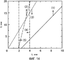
На диаграмме фиг.14 показана взаимосвязь между формулами (1)-(5).The diagram of Fig. 14 shows the relationship between formulas (1) to (5).
Для того чтобы понизить риск короткого замыкания, гребенчатый электрод может иметь группу общих электродов и группу пиксельных электродов, и группа общих электродов и группа пиксельных электродов могут быть расположены так, чтобы их разделял изолирующий слой.In order to reduce the risk of short circuit, the comb electrode may have a group of common electrodes and a group of pixel electrodes, and a group of common electrodes and a group of pixel electrodes can be arranged so that they are separated by an insulating layer.
Для того чтобы понизить питающее напряжение, т.е. обеспечить низковольтное управление, желательно, чтобы анизотропия диэлектрической проницаемости Δε нематического жидкого кристалла p-типа была равна 10 (более предпочтительно 15) или больше.In order to lower the supply voltage, i.e. to provide low-voltage control, it is desirable that the anisotropy of the dielectric constant Δ ε of the p- type nematic liquid crystal is 10 (more preferably 15) or more.
ПОЛЕЗНОСТЬ ИЗОБРЕТЕНИЯUSEFULNESS OF THE INVENTION
Жидкокристаллические дисплейные устройства настоящего изобретения могут обеспечивать превосходные показатели по ширине угла видимости и быстроте отклика, а также осуществлять индикацию на основе метода индикации, не требующего операции первичного продольно-изгибного перехода.The liquid crystal display devices of the present invention can provide excellent performance in terms of the width of the viewing angle and the speed of response, as well as provide an indication based on an indication method that does not require a primary bending transition operation.
В частности, гребенчатый электрод, удовлетворяющий соотношению (S+1,7)/(S+L)≥0,7, где L представляет собой ширину электрода, а S - расстояние между электродами, способен обеспечить показатели по ширине угла видимости, эквивалентные показателям, достигаемым по методам ВОМС и ПП; по быстроте отклика - эквивалентные или выше, чем показатели по методу ОСДЛ; а также высокий коэффициент пропускания и высокую контрастность.In particular, a comb electrode that satisfies the relation ( S +1.7) / ( S + L ) ≥0.7, where L represents the width of the electrode and S is the distance between the electrodes, is able to provide indicators for the width of the viewing angle equivalent to those achieved by the methods of VOMS and PP; by speed of response - equivalent or higher than indicators by the OSDL method; as well as high transmittance and high contrast.
Кроме того, по меньшей мере две области (первая область и вторая область) с различным для каждой отношением S/L межэлектродного расстояния S к ширине электродов L, расположенные в одном пикселе, способны обеспечить показатели по ширине угла видимости, эквивалентные показателям, достигаемым по методам ВОМС и ПП; по быстроте отклика - эквивалентные или выше, чем показатели по методу ОСДЛ, а также улучшение показателей для теневых зон шкал яркости.In addition, at least two regions (the first region and the second region) with a different S / L ratio of the interelectrode distance S to the width of the electrodes L , located in one pixel, are capable of providing indicators for the width of the viewing angle equivalent to those achieved by the methods VOMS and software; in terms of response speed - equivalent or higher than indicators according to the OSDL method, as well as improved indicators for shadow zones of brightness scales.
КРАТКОЕ ОПИСАНИЕ ЧЕРТЕЖЕЙBRIEF DESCRIPTION OF THE DRAWINGS
На фиг.1 схематически изображена в перспективе основная структура жидкокристаллических дисплейных устройств по Воплощению 1.Figure 1 schematically depicts in perspective a basic structure of liquid crystal display devices of
На фиг.2 показан в разрезе один из примеров распределения потенциала в ячейке, когда к жидкокристаллическому дисплейному устройству по Воплощению 1 приложено электрическое напряжение.Figure 2 shows a sectional view of one example of a potential distribution in a cell when an electric voltage is applied to the liquid crystal display device of
На фиг.3 показан в разрезе один из примеров распределения ориентации жидких кристаллов, когда к жидкокристаллическому дисплейному устройству по Воплощению 1 приложено напряжение.Figure 3 shows a sectional view of one example of a distribution of the orientation of liquid crystals when a voltage is applied to the liquid crystal display device of
На фиг.4 показана в разрезе основная структура жидкокристаллического индикаторного элемента из Примера 1.Figure 4 shows a sectional view of the main structure of the liquid crystal indicator element from Example 1.
На фиг.5 дан вид на плоскости для описания азимутов осей пропускания и направления наложенного электрического поля в жидкокристаллическом дисплейном устройстве из Примера 1.Figure 5 is a plane view for describing the azimuths of the transmission axes and the direction of the applied electric field in the liquid crystal display device of Example 1.
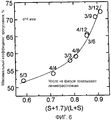
На диаграмме фиг.6 представлено отношение ширины электрода и межэлектродного расстояния к максимальному коэффициенту пропускания в жидкокристаллическом дисплейном устройстве из Примера 1.The diagram of Fig.6 shows the ratio of the electrode width and the interelectrode distance to the maximum transmittance in the liquid crystal display device of Example 1.
На фиг.7 графически представлена зависимость быстроты отклика от температуры в жидкокристаллическом дисплейном устройстве из Примера 1.Figure 7 graphically shows the dependence of the response speed on temperature in the liquid crystal display device of Example 1.
На фиг.8 показано в разрезе жидкокристаллическое дисплейное устройство по Воплощению 1 для пояснения быстроты отклика.FIG. 8 is a cross-sectional view of a liquid crystal display device according to
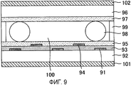
На фиг.9 показана в разрезе основная структура жидкокристаллического дисплейного устройства из Примера 3.Figure 9 shows a sectional view of the main structure of the liquid crystal display device of Example 3.
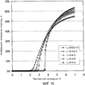
На диаграмме фиг.10 представлен график напряжения относительно коэффициента пропускания жидкокристаллического дисплейного устройства из Примера 4.The diagram of figure 10 presents a graph of the voltage relative to the transmittance of the liquid crystal display device of Example 4.
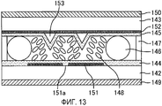
На фиг.11 схематически показан в разрезе индикаторный жидкокристаллический элемент по методу ВОМС из Сравнительного примера 2.11 is a schematic sectional view of an indicator liquid crystal element according to the VOMS method of Comparative Example 2.
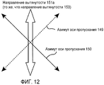
На фиг.12 дан вид на плоскости для описания азимутов осей пропускания и направления наложенного электрического поля в жидкокристаллическом дисплейном устройстве из Сравнительного примера 2.12 is a plane view for describing the azimuths of the transmission axes and the direction of the applied electric field in the liquid crystal display device of Comparative Example 2.
На фиг.13 показан схематический разрез для описания ориентации жидких кристаллов, когда напряжение приложено к жидкокристаллическому индикаторному элементу по методу ВОМС из Сравнительного примера 2.13 is a schematic sectional view for describing the orientation of liquid crystals when a voltage is applied to the liquid crystal indicator element according to the VOMS method of Comparative Example 2.
На фиг.14 графически показан предпочтительный диапазон для ширины электродов L и межэлектродного расстояния S в настоящем изобретении.On Fig graphically shows the preferred range for the width of the electrodes L and the interelectrode distance S in the present invention.
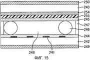
На фиг.15 схематически показана в разрезе основная структура индикаторного жидкокристаллического элемента из Примера 7.On Fig schematically shown in section the main structure of the indicator liquid crystal element from Example 7.
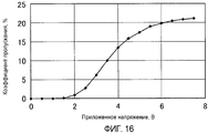
На диаграмме фиг.16 представлен график напряжения относительно коэффициента пропускания жидкокристаллического дисплейного устройства из Примера 7.The diagram of Fig.16 shows a graph of the voltage relative to the transmittance of the liquid crystal display device of Example 7.
СПОСОБ ОСУЩЕСТВЛЕНИЯ ИЗОБРЕТЕНИЯMODE FOR CARRYING OUT THE INVENTION
Настоящее изобретение описывается более подробно, со ссылками на чертежи и с указанием примеров воплощения, однако оно не ограничивается этими воплощениями.The present invention is described in more detail, with reference to the drawings and indicating examples of embodiments, however, it is not limited to these embodiments.
Воплощение 1
В жидкокристаллическом дисплейном устройстве настоящего изобретения распределение напряженности электрического поля формируется в ячейке, на которую наложено электрическое поле; вследствие этого обеспечивается ориентация продольного изгиба. Кроме того, электрическое поле в жидкокристаллическом дисплейном устройстве настоящего изобретения накладывается к перпендикулярно ориентированному нематическому жидкому кристаллу p-типа (нематический жидкий кристалл с положительной диэлектрической анизотропией) в поперечном направлении вдоль поверхностей подложек; наложенное таким образом электрическое поле обусловливает ориентацию продольного изгиба.In the liquid crystal display device of the present invention, an electric field strength distribution is formed in a cell over which an electric field is applied; as a result, the orientation of the longitudinal bend is ensured. In addition, an electric field in the liquid crystal display device of the present invention is superimposed on a perpendicularly oriented p- type nematic liquid crystal (nematic liquid crystal with positive dielectric anisotropy) in the transverse direction along the surfaces of the substrates; The electric field imposed in this way determines the orientation of the longitudinal bend.
На фиг.1 схематически изображена в перспективе основная структура жидкокристаллического дисплейного устройства по Воплощению 1. Вертикально ориентированные слои 13 и 14 помещены на две прозрачные подложки 11 и 12 соответственно. Когда электрическое поле не наложено, нематический жидкий кристалл p-типа (молекулы 15 жидкого кристалла) ориентирован гомеотропно. В частности, когда электрическое поле не наложено, молекулы 15 жидкого кристалла вблизи вертикально ориентированных слоев 13 и 14 ориентированы так, что их длинные оси практически перпендикулярны подложкам 11 и 12. Таким образом, угол предварительного наклона молекул 15 жидкого кристалла не требуется подгонять точно, при условии, что он приблизительно прямой относительно подложек. Для получения высокого контрастного отношения желательно, чтобы угол предварительного наклона был 88º или больше.Figure 1 schematically shows in perspective the basic structure of a liquid crystal display device according to
Подложки 11 и 12 могут быть из прозрачного стекла или пластика, обычно используемого для жидкокристаллических дисплейных устройств. В частности, предпочтительно, чтобы коэффициент пропускания подложек составлял 75% или больше (более предпочтительно 90% или больше), а матовость 5% или меньше (более предпочтительно 3% или меньше). В случае когда коэффициент пропускания подложек составляет 75% или больше, настоящее воплощение может использоваться для недорогих сенсорных экранов. В случае когда коэффициент пропускания подложек составляет 90% или больше, настоящее воплощение может использоваться для индикаторных жидкокристаллических панелей обычных жидкокристаллических дисплеев на тонкопленочных транзисторах.The
На подложке 12 помещается гребенчатый электрод 16, содержащий гребенчатую группу общих электродов и гребенчатую группу пиксельных электродов. Эти группы электродов располагаются так, чтобы они были обращены друг к другу и взаимно проникали в зазоры.On the
Группа общих электродов состоит из параллельных общих электродов, и общие электроды соединены друг с другом вблизи внешней границы пикселя (или точки). Группа общих электродов в любом пикселе получает единый сигнал (ниже называемый общим сигналом).A group of common electrodes consists of parallel common electrodes, and common electrodes are connected to each other near the outer border of the pixel (or point). A group of common electrodes in any pixel receives a single signal (hereinafter referred to as a common signal).
Группа пиксельных электродов тоже состоит из параллельных пиксельных электродов, и пиксельные электроды соединены друг с другом вблизи внешней границы пикселя (или точки). Группа пиксельных электродов располагается соответственно каждому пикселю (или точке). Группа пиксельных электродов любого пикселя получает в определенный момент времени сигнал изображения.The group of pixel electrodes also consists of parallel pixel electrodes, and the pixel electrodes are connected to each other near the outer border of the pixel (or point). A group of pixel electrodes is located respectively to each pixel (or point). A group of pixel electrodes of any pixel receives an image signal at a certain point in time.
Две подложки 11 и 12 снабжены также двумя поляризаторами 17 и 18 соответственно на основной внешней поверхности.Two
Подобная структура ячейки раскрыта в Патентном документе 1. В Патентных документах 3 и 4 раскрывается, что электрическое поле продольного изгиба образуется в результате наложения электрического поля, и образуются два домена с азимутами директоров, повернутыми на 180° относительно друг друга, благодаря чему могут достигаться хорошие показатели по ширине угла видимости.A similar cell structure is disclosed in
Однако известным структурам ячеек, раскрытым в Патентных документах 1 и 4, присущи проблемы, такие как высокое управляющее напряжение и низкий коэффициент пропускания ячеек, хотя у них превосходные показатели по углу видимости; таким образом, на практике они не используются.However, the well-known cell structures disclosed in
Учитывая такое положение дел, авторы изобретения изучили названные проблемы и обнаружили, что углом ориентации продольного изгиба можно управлять при помощи подходящей подгонки ширины электродов и внутриэлектродного (межэлектродного) расстояния. Благодаря этому впервые был получен высокий коэффициент пропускания при удобном управляющем напряжении.Given this state of affairs, the inventors studied these problems and found that the angle of orientation of the longitudinal bend can be controlled by a suitable fit of the width of the electrodes and the interelectrode (interelectrode) distance. Thanks to this, a high transmittance was first obtained at a convenient control voltage.
В отличие от стандартных изобретений, согласно настоящему изобретению, углом ориентации продольного изгиба можно свободно управлять. При этом, например, быстрота отклика может обеспечиваться благодаря жидкостным эффектам, как в случае метода ОСДЛ. Из сказанного следует, что настоящее изобретение имеет чрезвычайно высокую практическую ценность.Unlike standard inventions according to the present invention, the angle of orientation of the longitudinal bend can be freely controlled. In this case, for example, the response speed can be ensured due to liquid effects, as in the case of the OSDL method. It follows from the foregoing that the present invention has extremely high practical value.
По методу ОСДЛ молекулы жидкого кристалла переходят от ориентации поперечного изгиба к ориентации продольного изгиба при электрическом напряжении, чуть более высоком, чем критическое. При этом ориентация продольного изгиба имеет максимальную кривизну, и градационное отображение выполняется в промежутке между ориентацией продольного изгиба в этот момент времени и ориентацией слабого продольного изгиба при высоком приложенном электрическом напряжении.According to the OSDL method, liquid crystal molecules pass from the orientation of transverse bending to the orientation of longitudinal bending at an electric voltage slightly higher than critical. In this case, the longitudinal bending orientation has a maximum curvature, and gradation mapping is performed in the interval between the longitudinal bending orientation at this point in time and the orientation of the weak longitudinal bending at high applied electric voltage.
В противоположность этому в жидкокристаллическом дисплейном устройстве настоящего воплощения градационное отображение выполняется в промежутке между ориентацией продольного изгиба с большой кривизной, когда приложено высокое напряжение, и вертикальной ориентацией, когда напряжение не приложено. При этом максимальная кривизна зависит от приложенного напряжения: чем больше электрическое поле, тем больше максимальная кривизна. Другими словами, максимальной кривизной под действием приложенного высокого напряжения можно свободно управлять соответствующим выбором ширины электродов и межэлектродного расстояния. Таким образом, максимальную кривизну под действием приложенного высокого напряжения можно сделать больше, чем по методу ОСДЛ, а отклик более быстрым, чем может обеспечить метод ОСДЛ.In contrast, in the liquid crystal display device of the present embodiment, gradation display is performed between a longitudinal curvature with a large curvature when a high voltage is applied and a vertical orientation when a voltage is not applied. The maximum curvature depends on the applied voltage: the larger the electric field, the greater the maximum curvature. In other words, the maximum curvature under the action of the applied high voltage can be freely controlled by the appropriate choice of the width of the electrodes and the interelectrode distance. Thus, the maximum curvature under the action of the applied high voltage can be made greater than by the OSDL method, and the response is faster than the OSDL method can provide.
Здесь термин «кривизна» означает «степень деформации продольного изгиба», и это не физическое определение.Here, the term "curvature" means "the degree of deformation of longitudinal bending", and this is not a physical definition.
Если «степень деформации продольного изгиба» больше, чем требуется, ориентация продольного изгиба нарушается, как при перегибании ломается прут. В настоящем изобретении, наоборот, поверхностная энергия сцепления ориентированного слоя понижается, и благодаря этому может обеспечиваться более устойчивая ориентация продольного изгиба.If the "degree of deformation of the longitudinal bend" is greater than required, the orientation of the longitudinal bend is violated, as a rod breaks when bent. In the present invention, on the contrary, the surface adhesion energy of the oriented layer is reduced, and thereby a more stable longitudinal bending orientation can be provided.
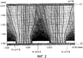
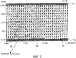
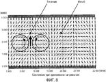
На фиг.2 показаны эквипотенциальные кривые в ячейке, когда приложено напряжение 7 В. При этом молекулы жидкого кристалла ориентируются в соответствии с этим распределением напряженности электрического поля и деформирующей силы со стороны поверхности раздела.Figure 2 shows the equipotential curves in the cell when a voltage of 7 V is applied. In this case, the liquid crystal molecules are oriented in accordance with this distribution of electric field strength and deforming force from the side of the interface.
На фиг.3 показано состояние жидкого кристалла в этот момент времени. Под действием приложенного напряжения молекулы жидкого кристалла непрерывно переходят от гомеотропной ориентации к ориентации продольного изгиба. Другими словами, в слое жидкого кристалла всегда обнаруживается ориентация продольного изгиба, и он может быстро отреагировать на нормальные управляющие сигналы изменением яркости различной степени. Из фиг.3 также видно, что степень деформации продольного изгиба выше, и потому выше скорость оптической модуляции, в области, где нет электрода, чем в области над электродом (гребенчатый электрод 16).Figure 3 shows the state of the liquid crystal at this point in time. Under the action of the applied voltage, the liquid crystal molecules continuously move from a homeotropic orientation to a longitudinal bending orientation. In other words, longitudinal bending orientation is always detected in the liquid crystal layer, and it can quickly respond to normal control signals by varying the brightness of various degrees. Figure 3 also shows that the degree of deformation of the longitudinal bend is higher, and therefore the speed of optical modulation is higher in the region where there is no electrode than in the region above the electrode (comb electrode 16).
Настоящее изобретение основано на открытии, что степенью этой ориентации продольного изгиба можно управлять посредством оптимизации структуры панели. По настоящему изобретению можно повышать степень продольного изгиба, обусловливая высокий коэффициент пропускания. Далее жидкокристаллическое дисплейное устройство настоящего изобретения обеспечивает возможность быстрого отклика, потому что течение молекул жидкого кристалла происходит в направлении, содействующем движению молекул жидкого кристалла, когда молекулам жидкого кристалла в настоящем воплощении следует двигаться, как в случае метода ОСДЛ.The present invention is based on the discovery that the degree of this longitudinal bending orientation can be controlled by optimizing the panel structure. According to the present invention, it is possible to increase the degree of longitudinal bending, resulting in a high transmittance. Further, the liquid crystal display device of the present invention provides a quick response, because the flow of liquid crystal molecules occurs in a direction that facilitates the movement of liquid crystal molecules when the liquid crystal molecules in the present embodiment should move, as in the case of the LDS method.
Ниже настоящее изобретение описывается более подробно со ссылками на чертежи и с примерами.Below the present invention is described in more detail with reference to the drawings and with examples.
Пример 1Example 1
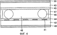
На фиг.4 изображена в разрезе основная структура индикаторного жидкокристаллического элемента из Примера 1. Несколько индикаторных жидкокристаллических элементов изготавливаются с различными ширинами электродов L и межэлектродными расстояниями S.Figure 4 shows a sectional view of the basic structure of an indicator liquid crystal element from Example 1. Several indicator liquid crystal elements are made with different electrode widths L and interelectrode distances S.
Сначала была изготовлена подложка 42, снабженная гребенчатым электродом 41, изготовленным из оксида олова-индия (ITO), шириной L, с межэлектродным расстоянием S. Ориентирующий слой покрытия JALS-204 (раствор 5 вес.% γ-бутиролактона фирмы JSR Corp.) был получен методом центрифугирования на подложке и затем отверждался 2 часа при 200°C. Таким образом был сформирован слой 44. Толщина ориентирующего слоя 44 составляла 60 нм. Таким же образом на стеклянной подложке 43 был сформирован ориентирующий слой 45 толщиной 60 нм из того же покрытия для ориентирующих слоев, что и слой 44.First, a
Потом по подложке 42 были распределены шарики смолы 46 диметром 4 мкм (Micropearl SP, Sekisui Chemical Co., Ltd.), а на подложу 43 впечатан смоляной герметик 47 (STRUCTBOND XN-21-S, Mitsui Toatsu Chemicals, Inc.). Эти подложки были скреплены друг с другом и отверждались 3 часа при 250°C. Таким образом была изготовлена жидкокристаллическая ячейка.Then,
После этого в жидкокристаллическую ячейку было внесено методом вакуумного впрыска жидкокристаллическое вещество 48 (SD-5654, Δε=16,2, Δn=0,099, Chisso Corp.) и прикреплены к ней поляризаторы 49 и 50. Таким образом были изготовлены жидкокристаллические индикаторные элементы для Примера 1.After that, a liquid crystal substance 48 (SD-5654, Δ ε = 16.2, Δ n = 0.099, Chisso Corp.) was introduced into the liquid crystal cell by vacuum injection and
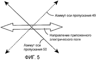
На фиг.5 показана взаимосвязь между направлением наложенного электрического поля и азимутами осей поляризаторов 49 и 50 в этом примере. Видно, что поляризаторы 49 и 50 были расположены, как скрещенные призмы Николя, а электрическое поле наложено в направлении биссектрисы угла, образованного осями пропускания поляризаторов 49 и 50.Figure 5 shows the relationship between the direction of the superimposed electric field and the azimuths of the axes of the
Фиг.6 показывает максимальный коэффициент пропускания каждого жидкокристаллического индикаторного элемента при комнатной температуре (25°C), когда приложен прямоугольный импульс 30 Гц с напряжением 0-20 В. По другой оси показано значение соотношения для участка, который вносит вклад в светопроводимость в ячейке. Величина 1,7 по формуле - это экспериментальная величина, и она показывает, что область между кромкой электрода и частью, отстоящей на 1,7 мкм от кромки электрода, вносит вклад в рост коэффициента пропускания. Числа на чертеже представляют величины отношения ширины электрода L к межэлектродному расстоянию S.6 shows the maximum transmittance of each liquid crystal indicator element at room temperature (25 ° C) when a rectangular pulse of 30 Hz with a voltage of 0-20 V is applied. The ratio for the portion that contributes to the light transmission in the cell is shown on the other axis. The value 1.7 by the formula is an experimental value, and it shows that the region between the edge of the electrode and the part 1.7 microns apart from the edge of the electrode contributes to the increase in transmittance. The numbers in the drawing represent the ratio of the electrode width L to the interelectrode distance S.
Здесь ширина электрода L представляет собой ширину участка, где общий электрод и пиксельный электрод обращены друг к другу (длина в поперечном направлении). Межэлектродное расстояние S представляет собой расстояние между общим электродом и смежным пиксельным электродом на участке, где общий электрод и пиксельный электрод обращены друг к другу.Here, the width of the electrode L is the width of the portion where the common electrode and the pixel electrode are facing each other (length in the transverse direction). The interelectrode distance S is the distance between the common electrode and the adjacent pixel electrode in a portion where the common electrode and the pixel electrode face each other.
Как показано на фиг.6, чем больше величина (S+1,7)/(S+L), тем выше максимальный коэффициент пропускания.As shown in FIG. 6, the larger the value ( S +1.7) / ( S + L ), the higher the maximum transmittance.
Современный метод ВОМС дает коэффициент пропускания около 80%, однако коэффициент пропускания жидкокристаллического слоя снижается до 50% или меньше вследствие больших светопотерь в областях ребристости и других факторов. У существующих жидкокристаллических панелей (изготовленных по методу ВОМС) коэффициент пропускания панели задается произведением апертурного отношения пикселя на коэффициент пропускания цветофильтра и коэффициенты пропускания поляризаторов. Таким образом коэффициент пропускания панели понижается до 4-5%.The modern VOMS method gives a transmittance of about 80%, but the transmittance of the liquid crystal layer is reduced to 50% or less due to large light losses in the areas of ribbing and other factors. For existing liquid crystal panels (manufactured by the VOMS method), the transmittance of the panel is specified by the product of the aperture ratio of the pixel by the transmittance of the color filter and the transmittance of the polarizers. Thus, the transmittance of the panel is reduced to 4-5%.
В результате очень важно знать, как увеличить насколько возможно коэффициент пропускания жидкокристаллического слоя (или коэффициент пропускания по данному методу).As a result, it is very important to know how to increase the transmittance of the liquid crystal layer (or the transmittance by this method) as much as possible.
Метод индикации по настоящему изобретению не требует ребристости. Так, метод индикации может осуществляться на практике в случае, если коэффициент пропускания слоя жидкого кристалла от 50 до 55% или больше. Коэффициент пропускания по методу, близкий к 50% или больше, как уже отмечалось, примерно соответствует уровню коэффициента пропускания панелей на основе современных методов индикации (например, метода ВОМС) и дает более яркое (менее энергопотребляющее) дисплейное устройство на жидких кристаллах. Даже если коэффициент пропускания по методу меньше 50%, настоящее изобретение имеет большую практическую ценность из-за простой структуры панелей и низкой стоимости их изготовления.The display method of the present invention does not require ribbing. Thus, an indication method may be practiced if the transmittance of the liquid crystal layer is from 50 to 55% or more. The transmittance by the method, close to 50% or more, as already noted, approximately corresponds to the transmittance of the panels based on modern display methods (for example, the VOMS method) and gives a brighter (less energy-consuming) liquid crystal display device. Even if the transmittance of the method is less than 50%, the present invention has great practical value due to the simple structure of the panels and the low cost of their manufacture.
Для простого повышения коэффициента пропускания может оказаться достаточным расширение межэлектродного расстояния S; однако расширение межэлектродного расстояния S увеличивает время отклика.To simply increase the transmittance, it may be sufficient to expand the interelectrode distance S ; however, the expansion of the interelectrode distance S increases the response time.
Фиг.6 показывает, что коэффициент пропускания можно повысить путем увеличения (S+1,7)/(S+L) без расширения межэлектродного расстояния S; настоящее изобретение впервые дает это преимущество.6 shows that the transmittance can be increased by increasing ( S +1,7) / ( S + L ) without expanding the interelectrode distance S ; the present invention provides this advantage for the first time.
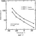
На фиг.7 показана зависимость быстроты отклика от температуры в случае, когда ширина электродов L равна 4 мкм и межэлектродное расстояние S равно 4 мкм. Как ясно из этого чертежа, настоящее изобретение дает быстрый отклик даже при низких температурах; таким образом, настоящее изобретение имеет большую практическую ценность.7 shows the dependence of the response speed on temperature in the case when the width of the electrodes L is 4 μm and the interelectrode distance S is 4 μm. As is clear from this drawing, the present invention provides a quick response even at low temperatures; thus, the present invention has great practical value.
Причина, по которой жидкокристаллический индикаторный элемент в жидкокристаллическом дисплейном устройстве настоящего изобретения дает быстрый отклик, состоит в том, что, когда приложено напряжение, молекулы жидкого кристалла поворачиваются и испытывают деформацию продольного изгиба.The reason that the liquid crystal display element in the liquid crystal display device of the present invention gives a quick response is because when the voltage is applied, the liquid crystal molecules rotate and experience buckling.
Как видно из фиг.8, течение (в направлении, показанном на фиг.8 стрелкой) происходит в слое жидкого кристалла, когда приложено напряжение. Здесь возникают вращения в нескольких направлениях, симметричных относительно линии дисклинации, или смещения с поворотом (темная линия), практически посередине между смежными общим электродом и пиксельным электродом. Около линии дисклинации крутящий момент действует в том же направлении. Поэтому, в отличие от метода СН и метода ВОМС, не возникает такого осложнения, когда одно течение в слое жидкого кристалла препятствует другому движению. Благодаря этому настоящее изобретение может обеспечить быстрый отклик подобно методу ОСДЛ.As can be seen from Fig. 8, the flow (in the direction shown by the arrow in Fig. 8) occurs in the liquid crystal layer when a voltage is applied. Here there are rotations in several directions, symmetrical about the disclination line, or displacement with rotation (dark line), almost in the middle between the adjacent common electrode and the pixel electrode. Near the disclination line, the torque acts in the same direction. Therefore, unlike the CH method and the VOMS method, there is no such complication when one flow in a layer of a liquid crystal impedes another movement. Due to this, the present invention can provide a quick response similar to the LDS method.
Такая высокая быстрота отклика соответствует степени деформации продольного изгиба (кривизне). Эта степень деформации продольного изгиба зависит от физических свойств жидкокристаллического вещества (особенно от анизотропии диэлектрической проницаемости Δε и коэффициента упругости); она зависит также от свойств гребенчатого электрода, таких как ширина электрода L и межэлектродное расстояние S, и от толщины слоя жидкого кристалла (глубины ячейки). Другими словами, по настоящему изобретению, степенью деформации продольного изгиба можно свободно управлять в соответствии с распределением напряженности электрического поля в ячейке. Поэтому отклик может получиться более быстрым, чем по методу ОСДЛ.Such a high response speed corresponds to the degree of deformation of longitudinal bending (curvature). This degree of buckling deformation depends on the physical properties of the liquid crystalline substance (especially on the dielectric constant anisotropy Δ ε and the coefficient of elasticity); it also depends on the properties of the comb electrode, such as the width of the electrode L and the interelectrode distance S , and on the thickness of the liquid crystal layer (cell depth). In other words, according to the present invention, the degree of buckling can be freely controlled in accordance with the distribution of the electric field strength in the cell. Therefore, the response may turn out to be faster than by the LDS method.
В качестве упомянутого выше жидкокристаллического вещества использовалось SD-5654 (Δε=16,2, Δn=0,099, Chisso Corp.), а приведенные экспериментальные результаты относились к опытной ячейке (глубина ячейки 4 мкм) c распределенными в ней шариками диаметром 4 мкм. Ниже описываются экспериментальные результаты относительно другой системы.SD-5654 (Δ ε = 16.2, Δ n = 0.099, Chisso Corp.) was used as the aforementioned liquid crystal substance, and the experimental results cited relate to the experimental cell (
Помимо этого в качестве жидкокристаллического вещества использовалось MJ08420X (Δε=12,9, Δn=0,10, Merck KGaA), и распределялись шарики диаметром 3,4 мкм; опытные ячейки (глубина ячейки 3,4 мкм) с различными отношениями ширины электрода L к межэлектродному расстоянию S изготавливались тем же способом, что описан выше. Характеристики напряжение-коэффициент пропускания снимались для каждой величины отношения ширины электрода L к межэлектродному расстоянию S. В Таблице 1 представлен коэффициент пропускания в случае приложенного напряжения 6 В.In addition, MJ08420X (Δ ε = 12.9, Δ n = 0.10, Merck KGaA) was used as a liquid crystal substance, and balls with a diameter of 3.4 μm were distributed; experimental cells (cell depth 3.4 μm) with different ratios of the electrode width L to the interelectrode distance S were made in the same manner as described above. The voltage-transmittance characteristics were measured for each value of the ratio of the electrode width L to the interelectrode distance S. Table 1 shows the transmittance in the case of an applied voltage of 6 V.
Таблица 1 показывает, что эта система также дает коэффициент пропускания 50% или больше при нормальных управляющих напряжениях (около нескольких вольт) при значении соотношения (S+1,7)/(S+L)≥0,7.Table 1 shows that this system also gives a transmittance of 50% or more at normal control voltages (around several volts) with a ratio value of ( S +1.7) / ( S + L ) ≥0.7.
Как отмечено выше, коэффициент пропускания возрастает по мере роста межэлектродного расстояния S; однако желательные эффекты по мере роста межэлектродного расстояния S постепенно приближаются к насыщению. Точнее говоря, с увеличением межэлектродного расстояния S растет управляющее напряжение и снижается быстрота отклика. Поэтому нецелесообразно увеличивать межэлектродное расстояние S сверх необходимого.As noted above, the transmittance increases with increasing interelectrode distance S ; however, the desired effects gradually increase towards saturation as the interelectrode distance S increases. More precisely, with an increase in the interelectrode distance S , the control voltage increases and the response speed decreases. Therefore, it is impractical to increase the interelectrode distance S in excess of the necessary.
Помимо этого в качестве жидкокристаллического вещества использовалось MJ0844X (Δε=20,0, Δn=0,12, Merck KGaA), и распределялись шарики диаметром 3,1 мкм; опытные ячейки (глубина ячейки 3,1 мкм) с различными отношениями межэлектродного расстояния S к ширине электрода L изготавливались тем же способом, что описан выше. Снимались их характеристики напряжение-коэффициент пропускания и время отклика для каждой величины отношения межэлектродного расстояния S к ширине электрода L. В Таблице 2 представлен коэффициент пропускания в случае приложенного напряжения 6,5 В.In addition, MJ0844X (Δ ε = 20.0, Δ n = 0.12, Merck KGaA) was used as a liquid crystal substance, and balls with a diameter of 3.1 μm were distributed; the experimental cells (cell depth 3.1 μm) with different ratios of the interelectrode distance S to the electrode width L were made in the same way as described above. Their characteristics were measured voltage-transmittance and response time for each value of the ratio of the interelectrode distance S to the width of the electrode L. Table 2 shows the transmittance in the case of an applied voltage of 6.5 V.
Из Таблицы 2 видно, что время отклика возрастает, а коэффициент пропускания убывает, когда отношение межэлектродного расстояния S к ширине электрода L больше 3,75. Поэтому характеристики индикации, наоборот, ухудшаются, если межэлектродное расстояние S увеличивается больше, чем нужно. Здесь снижение коэффициента пропускания обусловлено ослаблением электрического поля, вызванным увеличением межэлектродного расстояния S.From Table 2 it is seen that the response time increases and the transmittance decreases when the ratio of the interelectrode distance S to the electrode width L is greater than 3.75. Therefore, the characteristics of the display, on the contrary, deteriorate if the interelectrode distance S increases more than necessary. Here, the decrease in the transmittance is due to the weakening of the electric field caused by the increase in the interelectrode distance S.
Если ширина электрода L постоянна, скорость отклика и коэффициент пропускания находятся в оптимальном (компромиссном) соотношении. Чем меньше ширина электрода L, тем быстрее отклик и выше коэффициент пропускания. Однако с учетом наличия ограничений процесса (производства) в настоящее время ширина электрода L ограничена снизу пределом от 2 до 2,5 мкм. В этих условиях подходящей шириной электрода L является 2,5 мкм, а подходящим межэлектродным расстоянием S - от 7 до 8 мкм. Эти величины дают наиболее уравновешенные быстрый отклик и высокий коэффициент пропускания при ограничениях современного процесса (производства). В этом случае отношение (S/L) межэлектродного расстояния S к ширине электрода L лежит в пределах от 2,8 до 3,2.If the electrode width L is constant, the response speed and transmittance are in an optimal (compromise) ratio. The smaller the width of the electrode L , the faster the response and the higher the transmittance. However, given the limitations of the process (production), the electrode width L is currently limited from below to a limit of 2 to 2.5 μm. Under these conditions, a suitable electrode width L is 2.5 μm, and a suitable interelectrode distance S is from 7 to 8 μm. These values give the most balanced quick response and high transmittance with the limitations of the modern process (production). In this case, the ratio ( S / L ) of the interelectrode distance S to the width of the electrode L lies in the range from 2.8 to 3.2.
В случае когда ширина электрода L равна 2 мкм, а межэлектродное расстояние S равно 8 мкм, отношение S/L равно 4. Как видно из Таблицы 2, отношение S/L, равное 4, дает время отклика 12,8 мс; это время короче, чем используемое на практике время отклика 16 мс. Таким образом, отношение S/L, равное 4, также допускает отклик за время одного кадра.In the case where the electrode width L is 2 μm and the interelectrode distance S is 8 μm, the S / L ratio is 4. As can be seen from Table 2, the S / L ratio of 4 gives a response time of 12.8 ms; this time is shorter than the 16 ms response time used in practice. Thus, an S / L ratio of 4 also allows a response in one frame time.
Как указано выше, предпочтительное отношение S/L равно 4 или ниже, чтобы гарантировать практически используемое время отклика; предпочтительно отношение, равное 3,75 или ниже, чтобы эффективно снизить время отклика; и предпочтительно отношение 3,2 или ниже, чтобы соответствовать указанным выше ширине электрода L и межэлектродному расстоянию S (L=2,5 мкм, S=7-8 мкм) с учетом ограничений существующего (технологического) процесса.As indicated above, the preferred S / L ratio is 4 or lower to guarantee a practically usable response time; preferably a ratio of 3.75 or lower in order to effectively reduce the response time; and preferably a ratio of 3.2 or lower, to correspond to the above electrode width L and the interelectrode distance S ( L = 2.5 μm, S = 7-8 μm), taking into account the limitations of the existing (technological) process.
Пример 2Example 2
Жидкокристаллическая ячейка той же основной структуры, что и структура, показанная на фиг.4, с шириной электрода L, равной 4 мкм, межэлектродным расстоянием S, равным 4 мкм, и глубиной ячейки, равной 4 мкм, изготавливалась следующим способом.A liquid crystal cell of the same basic structure as the structure shown in FIG. 4, with an electrode width L of 4 μm, an interelectrode distance S of 4 μm, and a cell depth of 4 μm, was made as follows.
Сначала была изготовлена подложка 42, снабженная гребенчатым электродом 41, изготовленным из оксида олова-индия. Подложка была погружена на 5 минут в раствор вещества с кремнийводородными связями (силана) с формулой CF3-(CF2)17-SiCl3 (конц. 1 моль/л) в смеси хлороформа и N-метилпирролидона (NMP) (отношение по объему хлороформ:NMP=1:10), потом высушена в течение 1 часа при 120°C в сухом азоте. Таким образом был сформирован ориентирующий слой 44 (поверхностная энергия сцепления 5×10⁻⁵ Дж/м2).First, a
Тем же способом из того же вещества для ориентирующих слоев, которое использовалось для слоя 44, на подложке 43 был сформирован ориентирующий слой 45. Потом по подложке 42 были распределены капельки смолы 46 диметром 4 мкм (Micropearl SP, Sekisui Chemical Co., Ltd.), а на подложу 43 впечатан смоляной герметик 47 (STRUCTBOND XN-21-S, Mitsui Toatsu Chemicals, Inc.). Эти подложки были скреплены друг с другом и отверждались 3 часа при 250°C. Таким образом была изготовлена жидкокристаллическая ячейка.In the same way, from the same material for the orientation layers used for
После этого в жидкокристаллическую ячейку было внесено методом вакуумного впрыска жидкокристаллическое вещество 48 (ZLI-2293, Δε=10, Δn=0,136, Merck KGaA) и прикреплены к ней поляризаторы 49 и 50. Таким образом были изготовлены жидкокристаллические индикаторные элементы для Примера 2.After that, a liquid crystal substance 48 (ZLI-2293, Δ ε = 10, Δ n = 0.136, Merck KGaA) was introduced into the liquid crystal cell by vacuum injection, and
Взаимосвязь между направлением наложенного электрического поля и азимутами осей поляризаторов 49 и 50 в этом примере была такой же, как в Примере 1, и проиллюстрирована на фиг.5.The relationship between the direction of the superimposed electric field and the azimuths of the axes of the
Максимальный коэффициент пропускания жидкокристаллического индикаторного элемента из Примера 2 составлял 53% и делал возможной более яркую индикацию, чем по методу ВОМС с ребристой структурой и коэффициентом пропускания 42%. Таким образом, элемент имеет большую практическую ценность.The maximum transmittance of the liquid crystal indicator element from Example 2 was 53% and made possible a brighter indication than by the method of VOMS with a ribbed structure and transmittance of 42%. Thus, the element has great practical value.
Сравнительный пример 1Comparative Example 1
Помимо этого было использовано жидкокристаллическое вещество со свойствами Δε=15, Δn=0,1, k 11=11,2 пН, k 22=5,2 пН и k 33=15,6 пН; отношение L/S составляло 10 мкм/14 мкм, а глубина ячейки 7 мкм; индикаторный жидкокристаллический элемент для Сравнительного примера 1 был изготовлен с той же структурой, что элемент для Примера 1.In addition, a liquid crystal substance with the properties Δ ε = 15, Δ n = 0.1, k 11 = 11.2 pN, k 22 = 5.2 pN and k 33 = 15.6 pN was used; the L / S ratio was 10 μm / 14 μm and the cell depth was 7 μm; the indicator liquid crystal element for Comparative example 1 was made with the same structure as the element for Example 1.
Затем на индикаторный жидкокристаллический элемент подавались прямоугольные импульсы напряжения от 0-20 В частотой 30 Гц и измерялся максимальный коэффициент пропускания; величина составляла 34%. Кроме того, при подаче напряжения 7 В активационное время отклика (включения пикселя) составляло 20 мс, а время отклика на прекращение подачи напряжения 7 В составляло 25 мс; откликаемость индикаторного жидкокристаллического элемента оказалась неудовлетворительной.Then, rectangular voltage pulses from 0-20 V at a frequency of 30 Hz were applied to the indicator liquid crystal element and the maximum transmittance was measured; the value was 34%. In addition, when applying a voltage of 7 V, the activation response time (pixel on) was 20 ms, and the response time to stop supplying a voltage of 7 V was 25 ms; the response of the indicator liquid crystal element was unsatisfactory.
Здесь k 11, k 22 и k 33 - это упругие константы для поперечного изгиба, изгиба кручения и продольного изгиба соответственно.Here k 11 , k 22 and k 33 are elastic constants for lateral bending, torsion bending and longitudinal bending, respectively.
Пример 3Example 3
Индикаторные жидкокристаллические элементы A-E для Примера 3 были изготовлены тем же способом, что для Примера 1. У всех индикаторных элементов были разные ширины электродов L и межэлектродное расстояние S при толщине слоя жидкого кристалла 4 мкм.The indicator liquid crystal elements AE for Example 3 were manufactured in the same manner as for Example 1. All indicator elements had different electrode widths L and interelectrode distance S with a liquid crystal layer thickness of 4 μm.
На фиг.9 изображена в разрезе основная структура индикаторных жидкокристаллических элементов из Примера 3.Figure 9 shows a sectional view of the main structure of the indicator liquid crystal elements from Example 3.
В случае если группа общих электродов и группа пиксельных электродов расположены на одной плоскости, вероятность возникновения короткого замыкания возрастает с уменьшением межэлектродного расстояния S. Поэтому в настоящем примере между группой общих электродов и группой пиксельных электродов была методом вакуумного напыления сформирована в качестве изолятора пленка SiNx (толщина 2 мкм).If the group of common electrodes and the group of pixel electrodes are located on the same plane, the probability of a short circuit increases with decreasing interelectrode distance S. Therefore, in the present example, between the group of common electrodes and the group of pixel electrodes, a SiN x film (2 μm thick) was formed as an insulator by the vacuum deposition method.
Физические свойства использованного в эксперименте жидкокристаллического вещества производства фирмы Merck: анизотропия коэффициента преломления Δε=21 и двойное лучепреломление Δn=0,11.Physical properties of the Merck liquid crystal substance used in the experiment: anisotropy of the refractive index Δ ε = 21 and birefringence Δ n = 0.11.
Метод изготовления каждого из индикаторных жидкокристаллических элементов A-E описан ниже.The manufacturing method of each of the indicator liquid crystal elements A-E is described below.
Сначала была изготовлена подложка 92 и на подложке сформирована группа общих электродов 91. На них был нанесен методом вакуумного напыления слой SiNx 93, а поверх него сформирована группа пиксельных электродов 94. Полученная таким образом стеклянная подложка 92, снабженная гребенчатым электродом 41, изготовленным из оксида олова-индия, была погружена на 5 минут в раствор вещества с кремнийводородными связями (силана) с формулой CF3-(CF2)17-SiCl3 (конц. 1 моль/л) в смеси хлороформа и N-метилпирролидона (отношение по объему хлороформ:NMP=1:10). Потом подложка высушена в течение часа при 120°C в сухом азоте. Таким образом, был сформирован ориентирующий слой 95.First,
Тем же способом и с использованием тех же веществ, что и для ориентирующего слоя 95, был образован ориентирующий слой 97 на подложке 96.In the same manner and using the same substances as for the
После этого по подложке 92 были распределены капельки смолы 98 диаметром 4 мкм (Micropearl SP, Sekisui Chemical Co., Ltd.), а на подложу 96 впечатан смоляной герметик 99 (STRUCTBOND XN-21-S, Mitsui Toatsu Chemicals, Inc.). Эти подложки были скреплены друг с другом и отверждались 3 часа при 250°C. Таким образом была изготовлена жидкокристаллическая ячейка.After that, droplets of
Методом вакуумного впрыска в жидкокристаллическую ячейку было внесено жидкокристаллическое вещество 100 (Δε=21, Δn=0,106, Merck KGaA) и прикреплены к ней поляризаторы 101 и 102. Таким образом были изготовлены жидкокристаллические индикаторные элементы для Примера 3.By vacuum injection, a liquid crystal substance 100 (Δ ε = 21, Δ n = 0.106, Merck KGaA) was introduced into the liquid crystal cell and
Направление наложенного электрического поля и азимуты осей поляризаторов 101 и 102 в этом примере находятся в той же взаимосвязи, что в Примере 1, которая проиллюстрирована на фиг.5.The direction of the superimposed electric field and the azimuths of the axes of the
В Таблице 3 для индикаторных жидкокристаллических элементов A-E представлены характеристики электродов, максимальные коэффициенты пропускания время отклика затухания в случае прекращения приложения напряжения 6 В.Table 3 for indicator liquid crystal elements A-E shows the characteristics of the electrodes, the maximum transmittance, the response time of the attenuation in the event of the termination of the application of a voltage of 6 V.
У индикаторного жидкокристаллического элемента A слишком маленькая длина электрода, и произошел разрыв. Поэтому индикаторный жидкокристаллический элемент A не мог служить в качестве индикаторного жидкокристаллического элемента.The indicator liquid crystal element A has a too short electrode length and a break has occurred. Therefore, the indicator liquid crystal element A could not serve as the indicator liquid crystal element.
У каждого из индикаторных жидкокристаллических элементов B-D были высокие показатели коэффициента пропускания и удовлетворительное время отклика.Each of the B-D indicator liquid crystal elements had high transmittance and satisfactory response time.
У индикаторного жидкокристаллического элемента E был медленный отклик затухания, неподходящий для практического применения.The indicator liquid crystal element E had a slow attenuation response, unsuitable for practical use.
В настоящем примере использовался лишь один простой образец ориентирующего слоя, но, конечно же, допустимо использовать и традиционные полиамидные ориентирующие слои и неорганические ориентирующие слои, которые ориентируют молекулы жидкого кристалла согласно форме свой поверхности.In this example, only one simple sample of the orienting layer was used, but, of course, it is acceptable to use both traditional polyamide orienting layers and inorganic orienting layers, which orient the liquid crystal molecules according to the shape of their surface.
Тем не менее, процесс формирования мономолекулярной адсорбционной пленки может быть чрезвычайно простым, и благодаря этому можно получить однородный ориентирующий слой путем всего лишь погружения подложки в раствор.However, the process of forming a monomolecular adsorption film can be extremely simple, and due to this, a uniform orienting layer can be obtained by simply dipping the substrate in the solution.
По традиционным методам индикации следует формировать угол предварительного наклона; однако контролировать угол предварительного наклона для мономолекулярной адсорбционной пленки нелегко. В отличие от традиционных, согласно методу индикации настоящего изобретения требуется только, чтобы молекулы жидкого кристалла были ориентированы практически перпендикулярно. Поэтому весьма целесообразно использовать мономолекулярную адсорбционную пленку в методе индикации настоящего изобретения, который не требует контроля точности угла предварительного наклона.According to traditional methods of indication, an angle of preliminary inclination should be formed; however, it is not easy to control the preliminary tilt angle for a monomolecular adsorption film. Unlike traditional, according to the display method of the present invention, it is only required that the liquid crystal molecules are oriented almost perpendicularly. Therefore, it is highly advisable to use a monomolecular adsorption film in the display method of the present invention, which does not require control of the accuracy of the preliminary tilt angle.
Мономолекулярная адсорбционная пленка - это микропленка молекулярного уровня, и падение напряжения, обусловленное ориентирующей пленкой, вызывает меньшее. Следовательно, и в этом отношении мономолекулярная адсорбционная пленка также подходит для метода индикации настоящего изобретения.A monomolecular adsorption film is a microfilm of a molecular level, and the voltage drop caused by the orienting film causes a smaller one. Therefore, in this regard, the monomolecular adsorption film is also suitable for the display method of the present invention.
Пример 4Example 4
Помимо этого в качестве жидкокристаллического вещества был использован MJ08356 (Δε=20, Δn=0,1, Merck KGaA), и распределялись шарики диаметром 3,7 мкм; опытные ячейки (глубина ячейки 3,7 мкм) с различными отношениями межэлектродного расстояния S к ширине электрода L изготавливались тем же способом, что для Примера 1. Снимались их характеристики напряжение-коэффициент пропускания и время отклика для каждой величины отношения межэлектродного расстояния S к ширине электрода L. Здесь слой жидкого кристалла давал оптическую разность хода R th в поперечном направлении (по толщине), равную 260 нм.In addition, MJ08356 (Δ ε = 20, Δ n = 0.1, Merck KGaA) was used as a liquid crystal substance, and balls with a diameter of 3.7 μm were distributed; the experimental cells (cell depth 3.7 μm) with different ratios of the interelectrode distance S to the electrode width L were made in the same way as for Example 1. Their voltage-transmittance and response time characteristics were taken for each value of the ratio of the interelectrode distance S to the electrode width L. Here, the liquid crystal layer gave an optical path difference R th in the transverse direction (in thickness) of 260 nm.
Фиг.10 представляет собой диаграмму сравнения значений электрического напряжения относительно показателей коэффициента пропускания (для данного метода) жидкокристаллических дисплейных устройств из Примера 4.Figure 10 is a diagram comparing the values of the electrical voltage relative to the transmittance (for this method) of the liquid crystal display devices of Example 4.
Фиг.10 показывает, что максимальный коэффициент пропускания должен был, скорее всего, повышаться по мере роста величины отношения межэлектродного расстояния S к ширине электрода L (S/L), и рост должен становиться более крутым в области порогового напряжения, а яркостные характеристики ухудшаться в областях низкой яркости.Figure 10 shows that the maximum transmittance was most likely to increase as the ratio of the interelectrode distance S to the width of the electrode L ( S / L ) increased, and the growth should become steeper in the region of the threshold voltage, and the luminance characteristics deteriorate in areas of low brightness.
Для решения этих проблем полезно создать область, в которой показатели напряжение-коэффициент пропускания растут вблизи порогового напряжения умеренно, т.е. там, где отношение S/L относительно мало, в области пикселя. В этой области максимальный коэффициент пропускания падает, но яркостные показатели при малой яркости значительно улучшаются по сравнению с областью, где отношение S/L относительно велико. Поэтому дисплейное устройство на жидких кристаллах, содержащее области с различным значением S/L в каждой из них, имеет более значительную практическую ценность.To solve these problems, it is useful to create an area in which the voltage-transmittance indicators grow moderately near the threshold voltage, i.e. where the S / L ratio is relatively small, in the pixel area. In this region, the maximum transmittance decreases, but the brightness values at low brightness are significantly improved compared to the region where the S / L ratio is relatively large. Therefore, a liquid crystal display device containing regions with different S / L values in each of them has more significant practical value.
Кроме того, в конструкции с единственной величиной отношения S/L электроды могут не соответствовать пикселям. Использование сочетания двух или более величин отношения S/L приводит к эффективному использованию области пикселя. В частности, есть возможность ликвидировать мертвую зону, которую нужно формировать, если в пикселе нет места, куда можно приспособить пару электродов.In addition, in a design with a single S / L ratio, the electrodes may not correspond to pixels. Using a combination of two or more S / L ratios results in efficient use of the pixel region. In particular, it is possible to eliminate the dead zone, which must be formed if there is no place in the pixel where a pair of electrodes can be adapted.
Количество областей с различным значением S/L в каждой из них, располагающихся в одной пиксельной области, не ограничивается здесь конкретным числом. Решение о желательном количестве принимается в соответствии с показателями по углу видимости.The number of regions with different S / L values in each of them located in one pixel region is not limited to a specific number. The decision on the desired amount is made in accordance with indicators for the angle of visibility.
Пример 5Example 5
Индикаторный жидкокристаллический элемент для Примера 5 был изготовлен с той же структурой, которая показана в разрезе на фиг.4.The indicator liquid crystal element for Example 5 was made with the same structure as shown in section in FIG. 4.
Ширина электрода L и межэлектродное расстояние S были 3,0 мкм и 5,0 мкм соответственно, а глубина ячейки 3,0 мкм. То есть была задана величина (S+1,7)/(S+L) около 0,84.The electrode width L and the interelectrode distance S were 3.0 μm and 5.0 μm, respectively, and the cell depth was 3.0 μm. That is, the value ( S +1.7) / ( S + L ) was set to about 0.84.
Индикаторный жидкокристаллический элемент изготавливался тем же способом, что и для Примера 1. Жидкокристаллическое вещество MJ081029 (Δε=22,5, Δn=0,100, Merck KGaA) вводилось в индикаторный жидкокристаллический элемент методом вакуумного впрыска, и к элементу прикреплялись поляризаторы 49 и 50.The indicator liquid crystal element was manufactured in the same manner as for Example 1. The liquid crystal substance MJ081029 (Δ ε = 22.5, Δ n = 0.100, Merck KGaA) was introduced into the indicator liquid crystal element by vacuum injection, and
Направление наложенного электрического поля и азимуты осей поляризаторов 49 и 50 в этом примере соответствуют Примеру 1 и показаны на фиг.5.The direction of the superimposed electric field and the azimuths of the axes of the
На изготовленный таким образом индикаторный жидкокристаллический элемент подавался прямоугольный импульс напряжения 0-6 В частотой 30 Гц и измерялся максимальный коэффициент пропускания при комнатной температуре (25°C); его величина оказалась равной 62%.A rectangular pulse of a voltage of 0-6 V at a frequency of 30 Hz was applied to the indicator liquid crystal fabricated in this way, and the maximum transmittance was measured at room temperature (25 ° C); its value was equal to 62%.
В случае если жидкокристаллическое дисплейное устройство собрано из индикаторных жидкокристаллических элементов по настоящему примеру, подобно тому, как собирается традиционное дисплейное устройство на жидких кристаллах, яркость жидкокристаллических дисплейных устройств оценивается на основе этих величин по следующей схеме.In the case where the liquid crystal display device is assembled from the liquid crystal display elements of the present example, similar to how a traditional liquid crystal display device is assembled, the brightness of the liquid crystal display devices is estimated based on these values according to the following scheme.
Если коэффициент пропускания поляризатора равен 40%, коэффициент пропускания цветофильтра - 35%, апертурное отношение пикселя - 55%, а яркость фоновой подсветки - 5000 кд/м2, то яркость передней панели - 239 кд/м2. Для устройств типа портативных компьютеров (лэптопов) это подходящая яркость. Разумеется, в таких устройствах, как телевизоры, для которых требуется более высокая яркость, можно применить более яркую фоновую подсветку.If the transmittance of the polarizer is 40%, the transmittance color filter - 35%, the pixel aperture ratio - 55%, and the brightness of the backlight - 5000 cd / m 2, the brightness of the front panel - 239 cd / m 2. For devices such as laptop computers (laptops), this is the appropriate brightness. Of course, in devices such as televisions that require higher brightness, brighter backlighting can be applied.
Сравнительный пример 2Reference Example 2
В качестве сравнительного примера для Примера 5 был изготовлен индикаторный жидкокристаллический элемент по методу ВОМС со структурой, показанной на фиг.11.As a comparative example, Example 5 was made indicator liquid crystal element according to the method of VOMS with the structure shown in Fig.11.
Вначале была изготовлена стеклянная подложка 142, снабженная прозрачным электродом 151 с щелью 151a шириной 3,0 мкм. На подложку 142 методом центрифугирования был нанесен ориентирующий слой покрытия JALS-204 (раствор 5 вес.% γ-бутироактона, JSR Corp.) и отверждался 2 часа при 200°C. Таким образом был сформирован ориентирующий слой 144. В данном примере толщина ориентирующего слоя 144 составляла 60 нм.Initially, a
Одновременно была изготовлена стеклянная подложка 143, снабженная прозрачным электродом 152. Выступ 153, вытянутый в направлении, перпендикулярном плоскости чертежа фиг.11, был сформирован методом фотолитографии. Потом на подложку 143 методом центрифугирования был нанесен ориентирующий слой покрытия JALS-204 (раствор 5 вес.% γ-бутироактона, JSR Corp.) и отверждался 2 часа при 200°C. Таким образом был сформирован ориентирующий слой 145. В данном примере толщина ориентирующего слоя 145 составляла 60 нм.At the same time, a
На следующем этапе по подложке 142 были распределены капельки смолы 146 диметром 4 мкм (Micropearl SP, Sekisui Chemical Co., Ltd.), а на подложу 143 впечатан смоляной герметик 147 (STRUCTBOND XN-21-S, Mitsui Toatsu Chemicals, Inc.). Эти подложки были скреплены друг с другом и отверждались 3 часа при 250°C. Таким образом была изготовлена жидкокристаллическая ячейка.In the next step, droplets of
После этого в жидкокристаллическую ячейку было внесено методом вакуумного впрыска жидкокристаллическое вещество 148 (MLC-6608, Δε=-4,2, Δn=0,083, Merck KGaA) и прикреплены к ней поляризаторы 149 и 150. Таким образом были изготовлены жидкокристаллические индикаторные элементы для Сравнительного примера 2.After that, a liquid crystal substance 148 (MLC-6608, Δ ε = -4.2, Δ n = 0.083, Merck KGaA) was introduced into the liquid crystal cell by vacuum injection, and
На фиг.12 показана взаимосвязь между направлением щели 151 (тем же, что и направление выступа 153) и азимутами осей поляризаторов 149 и 150 в этом примере.12 shows the relationship between the direction of the slit 151 (the same as the direction of the protrusion 153) and the azimuths of the axes of the
Затем на верхний и нижний электроды (прозрачные электроды 151 и 152) было подано напряжение 6 В. Коэффициент пропускания в данном случае составил 45%. На фиг.13 показано состояние углового смещения (поворота), в которое при этом перешли молекулы жидкого кристалла 148.Then, a voltage of 6 V was applied to the upper and lower electrodes (
Согласно современному методу ВОМС, если коэффициент пропускания поляризатора - 40%, коэффициент пропускания цветофильтра - 35%, апертурное отношение пикселя - 55%, а яркость фоновой подсветки - 5000 кд/м2, то яркость передней панели, которая получается равной 173 кд/м2, неудовлетворительна. Поэтому в современном методе ВОМС помимо фоновой подсветки используется одна или более пленок, оптимизирующих яркость, благодаря чему яркость возрастает до 250 кд/м2.According to the modern VOMS method, if the transmittance of the polarizer is 40%, the transmittance of the color filter is 35%, the aperture ratio of the pixel is 55%, and the brightness of the backlight is 5000 cd / m 2 , then the brightness of the front panel, which is equal to 173 cd / m 2 , unsatisfactory. Therefore, in the present method besides BOMCA backlight, one or more films that optimize brightness, thereby increasing the brightness of 250 cd / m 2.
Как видно из Примера 5 и Сравнительного примера 2, индикаторный жидкокристаллический элемент из Примера 5 способен давать высокий коэффициент пропускания и не нуждается в пленке, оптимизирующей яркость и способной обусловить увеличение стоимости.As can be seen from Example 5 and Comparative example 2, the indicator liquid crystal element from Example 5 is able to give a high transmittance and does not need a film that optimizes brightness and can cause an increase in cost.
Таким образом, настоящий индикаторный элемент имеет исключительную практическую ценность.Thus, the present indicator element has exceptional practical value.
Пример 6Example 6
Индикаторный жидкокристаллический элемент для Примера 6 был изготовлен с той же структурой, которая схематически показана в разрезе на фиг.4.The indicator liquid crystal element for Example 6 was made with the same structure, which is schematically shown in section in figure 4.
Ширина электрода L и межэлектродное расстояние S составляли 2,5 мкм и 2,0 мкм соответственно, а глубина ячейки 3,3 мкм. То есть была задана величина (S+1,7)/(S+L) около 0,92.The electrode width L and the interelectrode distance S were 2.5 μm and 2.0 μm, respectively, and the cell depth was 3.3 μm. That is, the value ( S +1.7) / ( S + L ) was set to about 0.92.
Индикаторный жидкокристаллический элемент изготавливался тем же способом, что и для Примера 1. Жидкокристаллическое вещество MJ072330 (Δε=22,3, Δn=0,1220, Merck KGaA) вводилось в индикаторный жидкокристаллический элемент методом вакуумного впрыска, и к элементу прикреплялись поляризаторы 49 и 50.The indicator liquid crystal element was manufactured in the same manner as for Example 1. The liquid crystal substance MJ072330 (Δ ε = 22.3, Δ n = 0.1220, Merck KGaA) was introduced into the indicator liquid crystal element by vacuum injection, and
Направление наложенного электрического поля и азимуты осей поляризаторов 49 и 50 в этом примере соответствуют примеру 1 и показаны на фиг.5.The direction of the superimposed electric field and the azimuths of the axes of the
На изготовленный таким образом индикаторный жидкокристаллический элемент подавался прямоугольный импульс напряжения 0-6 В частотой 30 Гц и измерялся максимальный коэффициент пропускания при комнатной температуре (25°C); ее величина оказалась равной 72%.A rectangular pulse of a voltage of 0-6 V at a frequency of 30 Hz was applied to the indicator liquid crystal fabricated in this way, and the maximum transmittance was measured at room temperature (25 ° C); its value was equal to 72%.
В случае если жидкокристаллическое дисплейное устройство собрано из индикаторных жидкокристаллических элементов по настоящему примеру, подобно тому, как собирается традиционное жидкокристаллическое дисплейное устройство, яркость жидкокристаллического дисплейного устройства оценивается на основе этих величин по следующей схеме.In the case where the liquid crystal display device is assembled from the indicator liquid crystal elements of the present example, similar to how the traditional liquid crystal display device is assembled, the brightness of the liquid crystal display device is estimated based on these values according to the following scheme.
Если коэффициент пропускания поляризатора равен 40%, коэффициент пропускания цветофильтра - 35%, апертурное отношение пикселя - 55%, а яркость фоновой подсветки - 5000 кд/м2, то яркость панели спереди - 277 кд/м2. Эта величина примерно на 16% превышает яркость 239 кд/м2, достигнутую в Примере 5.If the transmittance of the polarizer is 40%, the transmittance color filter - 35%, the pixel aperture ratio - 55%, and the brightness of the backlight - 5000 cd / m2, the panel front brightness - 277 cd / m 2. This value is approximately 16% higher than the brightness of 239 cd / m 2 achieved in Example 5.
Производимые в настоящее время телевизоры с 40-дюймовым жидкокристаллическим экраном содержат от 15 до 20 флуоресцентных ламп c холодным катодом (CCFL). Поэтому данная величина означает, что в соответствии с настоящим примером число ламп можно сократить на 2 или 3. Настоящий пример имеет большую практическую ценность в смысле экономии ресурсов и снижения стоимости.40-inch LCD televisions currently in production contain between 15 and 20 cold cathode fluorescent lamps (CCFLs). Therefore, this value means that in accordance with this example, the number of lamps can be reduced by 2 or 3. This example has great practical value in terms of saving resources and reducing costs.
Пример 7Example 7
На фиг.15 схематически показана в разрезе основная структура индикаторного жидкокристаллического элемента из Примера 7.On Fig schematically shown in section the main structure of the indicator liquid crystal element from Example 7.
Была изготовлена подложка 242 (нижняя стеклянная подложка), снабженная гребенчатым электродом 241, изготовленным из оксида олова-индия, шириной L, равной 2,6 мкм, с межэлектродным расстоянием S, равным 5,0 мкм. Ориентирующий слой покрытия JALS-204 (раствор 5 вес.% γ-бутиролактона фирмы JSR Corp.) был получен методом центрифугирования на подложке и затем отверждался 2 часа при 200°C. Таким образом был сформирован слой 244 (нижний ориентирующий слой). В этом примере толщина ориентирующего слоя 244 составляла 60 нм.A substrate 242 (lower glass substrate) was made, provided with a
Была приготовлена стеклянная подложка 243 (верхняя подложка) со сформированным на ней зеленым цветофильтром 254 толщиной 2,0 мкм. На подложке был сформирован также выравнивающий слой 255 из отверждаемого ультрафиолетом акрилата (ε=3,7) (органический изолятор) толщиной 300 нм.A glass substrate 243 (upper substrate) was prepared with a
Ориентирующий слой 245 (верхний ориентирующий слой) толщиной 60 нм из покрытия JALS-204 был сформирован подобно слою на подложке 242.An orientation layer 245 (upper orientation layer) 60 nm thick from the JALS-204 coating was formed like a layer on the
Потом по подложке 242 были распределены капельки смолы 246 диметром 3,7 мкм (Micropearl SP, Sekisui Chemical Co., Ltd.), а на подложу 243 впечатан смоляной герметик 247 (STRUCTBOND XN-21-S, Mitsui Toatsu Chemicals, Inc.). Эти подложки были скреплены друг с другом и отверждались 3 часа при 250°C. Таким образом была изготовлена жидкокристаллическая ячейка.Then, 246 resin droplets were distributed on
Методом вакуумного впрыска в жидкокристаллическую ячейку было внесено жидкокристаллическое вещество 248 (MJ08356, Δε=20, Δn=0,1, Merck KGaA) и прикреплены к ней поляризаторы 250 (верхний поляризатор) и 249 (нижний поляризатор). Таким образом были изготовлены жидкокристаллические индикаторные элементы для Примера 7.By vacuum injection, a liquid crystal substance 248 (MJ08356, Δ ε = 20, Δ n = 0.1, Merck KGaA) was introduced into the liquid crystal cell and polarizers 250 (upper polarizer) and 249 (lower polarizer) were attached to it. Thus, liquid crystal display elements for Example 7 were made.
Направление наложенного электрического поля и азимуты осей двух поляризаторов 249 и 250 в этом примере соответствуют аналогичным направлению и азимутам из Примера 1 (см. фиг.5). То есть два поляризатора 249 и 250 были расположены в положении скрещенных призм Николя, а электрическое поле наложено в направлении биссектрисы угла, образованного осями пропускания поляризаторов 249 и 250.The direction of the superimposed electric field and the azimuths of the axes of the two
На диаграмме фиг.16 представлен график характеристик напряжения относительно коэффициента пропускания жидкокристаллических дисплейных устройств из Примера 7.The diagram of Fig.16 shows a graph of the voltage characteristics relative to the transmittance of the liquid crystal display devices of Example 7.
Из результатов, представленных на фиг.16, видно, что настоящее изобретение способно дополнительно понизить напряжение по сравнению с понижением, которое соответствует светлым квадратам (□) на фиг.10 (L/S=2,6/5). Предположительно это обусловлено следующим. Благодаря органическому изолятору (выравнивающий слой 255), сформированному на поверхности подложки 243, силовые линии электрического поля входят в поверхность подложки 243, и потому молекулы жидкого кристалла в окрестности выравнивающего слоя 245, скорее всего, должны поворачиваться на поверхности подложки 243.From the results presented in FIG. 16, it can be seen that the present invention is able to further lower the voltage compared to a decrease, which corresponds to the bright squares (□) in FIG. 10 ( L / S = 2.6 / 5). Presumably this is due to the following. Due to the organic insulator (leveling layer 255) formed on the surface of the
В настоящем изобретении в качестве вещества для выравнивающего слоя 255 использовался акрилат, отверждаемый ультрафиолетовым излучением. Веществом выравнивающего слоя могут быть органические слои, содержащие ненасыщенные карбоновые кислоты, такие как акриловая кислота и метакриловая кислота, или их эфиры; либо амиды, такие как акриламид и метакриламид, либо, разумеется, их производные. В качестве вещества выравнивающего слоя подходят также выравнивающие смолы (покрытия), такие как тугоплавкие полиамидные смолы.In the present invention, UV curing acrylate was used as a substance for the
Настоящее приложение является заявкой на приоритет к Патентной заявке № 2008-168593, поданной в Японии 27 июня 2008 года согласно Парижской конвенции и положениям национального закона указанного государства. Полное содержание заявки включено в описание путем ссылки.This annex is a priority application to Patent Application No. 2008-168593 filed in Japan on June 27, 2008 in accordance with the Paris Convention and the provisions of the national law of that state. The full content of the application is incorporated into the description by reference.
СПИСОК ОБОЗНАЧЕНИЙLIST OF DESIGNATIONS
11, 12, 42, 43, 92, 96, 142, 143, 242, 243 - подложка11, 12, 42, 43, 92, 96, 142, 143, 242, 243 - substrate
13, 14, 44, 45, 95, 97, 144, 145, 244, 245 - ориентирующий слой13, 14, 44, 45, 95, 97, 144, 145, 244, 245 - orientation layer
15, 48, 100, 248 - жидкий кристалл (нематический ЖК p-типа)15, 48, 100, 248 - liquid crystal (nematic LC p- type)
16, 41, 91, 94, 241 - электрод (гребенчатый электрод)16, 41, 91, 94, 241 - electrode (comb electrode)
17, 18, 49, 50, 101, 102, 149, 150, 249, 250 - поляризатор17, 18, 49, 50, 101, 102, 149, 150, 249, 250 - polarizer
46, 98, 146, 246 - сферический разделитель46, 98, 146, 246 - spherical separator
47, 99, 147, 247 - герметик47, 99, 147, 247 - sealant
93 - изолятор93 - insulator
148 - жидкий кристалл (ЖК n-типа)148 - liquid crystal (LC n- type)
151, 152 - прозрачный электрод151, 152 - transparent electrode
151a - щель151a - slot
153 - выступ (ребро)153 - ledge (rib)
254 - цветофильтр254 - color filter
255 - выравнивающий слой255 - leveling layer
Claims (16)
две подложки, по меньшей мере одна из которых прозрачна; и нематический жидкий кристалл р-типа, помещенный между двумя подложками,
причем нематический жидкий кристалл р-типа выровнен перпендикулярно к поверхностям двух подложек, когда не приложено напряжение; причем по меньшей мере одна из двух подложек имеет гребенчатый электрод;
причем гребенчатый электрод удовлетворяет соотношению
(S+1,7)/(S+L)≥0,7, где L представляет собой ширину электрода, a S
представляет собой расстояние между электродами; и
пиксель, имеющий первую область и вторую область,
причем первая область или вторая область имеет просветный участок,
занимающий 50% или больше просветного участка пикселя.1. A liquid crystal display device comprising:
two substrates, at least one of which is transparent; and a p-type nematic liquid crystal placed between two substrates,
wherein the p-type nematic liquid crystal is aligned perpendicular to the surfaces of the two substrates when no voltage is applied; moreover, at least one of the two substrates has a comb electrode;
moreover, the comb electrode satisfies the relation
(S + 1.7) / (S + L) ≥0.7, where L represents the width of the electrode, a S
represents the distance between the electrodes; and
a pixel having a first region and a second region,
wherein the first region or the second region has a lumen region,
occupying 50% or more of the luminous region of the pixel.
группа общих электродов и группа пиксельных электродов расположены через изолирующий слой.6. The liquid crystal display device according to claim 1, wherein: the comb electrode includes a group of common electrodes and a group of pixel electrodes; and
a group of common electrodes and a group of pixel electrodes are arranged through an insulating layer.
причем нематический жидкий кристалл р-типа выровнен перпендикулярно к поверхностям двух подложек, когда не приложено напряжение; причем по меньшей мере одна из двух подложек имеет гребенчатый электрод; и
пиксель, имеющий первую область и вторую область, которая имеет отношение S/L между шириной L электрода и расстоянием S между электродами гребенчатого электрода, отличное от такого отношения первой области.
причем первая область или вторая область имеет просветный участок, занимающий 50% или больше просветного участка пикселя.9. A liquid crystal display device, comprising: two substrates, at least one of which is transparent; and a p-type nematic liquid crystal placed between two substrates,
wherein the p-type nematic liquid crystal is aligned perpendicular to the surfaces of the two substrates when no voltage is applied; moreover, at least one of the two substrates has a comb electrode; and
a pixel having a first region and a second region that has an S / L ratio between the width of the electrode L and the distance S between the electrodes of the comb electrode, different from that of the first region.
moreover, the first region or the second region has a luminous region occupying 50% or more of the luminous region of the pixel.
группа общих электродов и группа пиксельных электродов расположены через изолирующий слой.14. The liquid crystal display device according to claim 9, in which: the comb electrode includes a group of common electrodes and a group of pixel electrodes; and
a group of common electrodes and a group of pixel electrodes are arranged through an insulating layer.
Applications Claiming Priority (3)
| Application Number | Priority Date | Filing Date | Title |
|---|---|---|---|
| JP2008168593 | 2008-06-27 | ||
| JP2008-168593 | 2008-06-27 | ||
| PCT/JP2009/059899 WO2009157271A1 (en) | 2008-06-27 | 2009-05-29 | Liquid crystal display device |
Publications (2)
| Publication Number | Publication Date |
|---|---|
| RU2011102970A RU2011102970A (en) | 2012-08-10 |
| RU2469366C2 true RU2469366C2 (en) | 2012-12-10 |
Family
ID=41444341
Family Applications (1)
| Application Number | Title | Priority Date | Filing Date |
|---|---|---|---|
| RU2011102970/28A RU2469366C2 (en) | 2008-06-27 | 2009-05-29 | Liquid crystal display device |
Country Status (7)
| Country | Link |
|---|---|
| US (1) | US20110063558A1 (en) |
| EP (1) | EP2290437B1 (en) |
| JP (1) | JP5178831B2 (en) |
| CN (1) | CN102317849B (en) |
| BR (1) | BRPI0914672A2 (en) |
| RU (1) | RU2469366C2 (en) |
| WO (1) | WO2009157271A1 (en) |
Families Citing this family (13)
| Publication number | Priority date | Publication date | Assignee | Title |
|---|---|---|---|---|
| RU2474853C2 (en) | 2008-10-14 | 2013-02-10 | Шарп Кабусики Кайся | Liquid crystal display device |
| CN102282506B (en) * | 2009-05-27 | 2014-06-04 | 夏普株式会社 | Liquid crystal display device |
| US8750857B2 (en) * | 2010-06-04 | 2014-06-10 | Qualcomm Incorporated | Method and apparatus for wireless distributed computing |
| WO2012011443A1 (en) * | 2010-07-22 | 2012-01-26 | シャープ株式会社 | Liquid crystal panel and liquid crystal display device |
| JP2012118329A (en) * | 2010-12-01 | 2012-06-21 | Lg Display Co Ltd | Liquid crystal display device |
| JP5621625B2 (en) * | 2011-01-28 | 2014-11-12 | コニカミノルタ株式会社 | Liquid crystal display |
| US9360697B2 (en) * | 2011-09-12 | 2016-06-07 | Sharp Kabushiki Kaisha | Liquid-crystal display panel and liquid-crystal display device |
| CN102629041B (en) * | 2012-02-09 | 2014-04-16 | 京东方科技集团股份有限公司 | Three-dimensional (3D) display device and manufacture method thereof |
| CN102629607B (en) * | 2012-02-09 | 2016-02-10 | 京东方科技集团股份有限公司 | Array base palte and dual field of view display device and manufacture method thereof |
| US9977294B2 (en) | 2012-06-25 | 2018-05-22 | Industry-University Cooperation Foundation Hanyang University | Liquid crystal display device |
| KR20140001071A (en) | 2012-06-25 | 2014-01-06 | 한양대학교 산학협력단 | Liquid crystal compound |
| WO2014013899A1 (en) * | 2012-07-20 | 2014-01-23 | 東洋紡株式会社 | Conductive paste for laser etching, conductive thin film, and conductive laminate |
| CN104487889B (en) * | 2012-07-25 | 2017-03-08 | 夏普株式会社 | Liquid crystal indicator |
Citations (4)
| Publication number | Priority date | Publication date | Assignee | Title |
|---|---|---|---|---|
| SU917164A1 (en) * | 1980-08-18 | 1982-03-30 | Организация П/Я В-8466 | Electric-optical device for displaying information |
| JPH10186351A (en) * | 1996-12-24 | 1998-07-14 | Hitachi Ltd | Liquid crystal display device |
| JPH11326955A (en) * | 1997-12-08 | 1999-11-26 | Hyundai Electronics Ind Co Ltd | Liquid crystal display device |
| JP2000081641A (en) * | 1998-06-23 | 2000-03-21 | Fujitsu Ltd | Liquid crystal display device |
Family Cites Families (21)
| Publication number | Priority date | Publication date | Assignee | Title |
|---|---|---|---|---|
| JPH024068A (en) | 1988-06-21 | 1990-01-09 | Nippon Hoso Kyokai <Nhk> | Packet multiplexer |
| JP3001695B2 (en) | 1991-04-04 | 2000-01-24 | 日東電工株式会社 | Wound dressing |
| TW434443B (en) * | 1997-05-30 | 2001-05-16 | Samsung Electronics Co Ltd | Liquid crystal display |
| CN1567066B (en) | 1997-05-30 | 2010-05-12 | 三星电子株式会社 | Liquid crystal display |
| US6704083B1 (en) * | 1997-05-30 | 2004-03-09 | Samsung Electronics, Co., Ltd. | Liquid crystal display including polarizing plate having polarizing directions neither parallel nor perpendicular to average alignment direction of molecules |
| KR100375732B1 (en) * | 1997-11-25 | 2004-10-14 | 비오이 하이디스 테크놀로지 주식회사 | Liquid crystal display device comprising a liquid crystal driving electrode, specially regarding to effectively letting out static electricity |
| KR100293809B1 (en) * | 1998-05-29 | 2001-10-26 | 박종섭 | Ips-va mode liquid crystal display having multi domain |
| US6642984B1 (en) * | 1998-12-08 | 2003-11-04 | Fujitsu Display Technologies Corporation | Liquid crystal display apparatus having wide transparent electrode and stripe electrodes |
| JP2000275682A (en) | 1999-03-26 | 2000-10-06 | Seiko Epson Corp | Liquid crystal device and electronic instrument using the same |
| KR20050061610A (en) * | 1999-06-11 | 2005-06-22 | 마쯔시다덴기산교 가부시키가이샤 | Liquid crystal display |
| JP3634249B2 (en) * | 1999-09-24 | 2005-03-30 | シャープ株式会社 | Liquid crystal display device and display method thereof |
| KR100433596B1 (en) * | 1999-10-21 | 2004-05-31 | 마쯔시다덴기산교 가부시키가이샤 | Liquid crystal device |
| JP2002055357A (en) | 2000-08-09 | 2002-02-20 | Casio Comput Co Ltd | Liquid crystal display |
| JP4368515B2 (en) * | 2000-10-31 | 2009-11-18 | シャープ株式会社 | LCD panel |
| JP4047586B2 (en) * | 2002-01-10 | 2008-02-13 | Nec液晶テクノロジー株式会社 | Horizontal electric field type active matrix liquid crystal display device |
| CN100442128C (en) * | 2003-07-14 | 2008-12-10 | 株式会社日立显示器 | Display device |
| US7107936B2 (en) * | 2003-09-04 | 2006-09-19 | Mmi Genomics, Inc. | Device and method for animal tracking |
| JP4245036B2 (en) * | 2006-10-31 | 2009-03-25 | エプソンイメージングデバイス株式会社 | Liquid crystal display |
| JP4453694B2 (en) * | 2006-10-31 | 2010-04-21 | セイコーエプソン株式会社 | Liquid crystal device and electronic device |
| JP2008168593A (en) | 2007-01-15 | 2008-07-24 | Fujifilm Corp | Method for manufacturing planographic printing plate |
| JP2011149966A (en) * | 2008-05-12 | 2011-08-04 | Sharp Corp | Liquid crystal display device |
-
2009
- 2009-05-29 JP JP2010517833A patent/JP5178831B2/en active Active
- 2009-05-29 WO PCT/JP2009/059899 patent/WO2009157271A1/en active Application Filing
- 2009-05-29 CN CN200980113309.9A patent/CN102317849B/en active Active
- 2009-05-29 BR BRPI0914672A patent/BRPI0914672A2/en not_active IP Right Cessation
- 2009-05-29 EP EP09769981.3A patent/EP2290437B1/en not_active Not-in-force
- 2009-05-29 US US12/993,151 patent/US20110063558A1/en not_active Abandoned
- 2009-05-29 RU RU2011102970/28A patent/RU2469366C2/en not_active IP Right Cessation
Patent Citations (4)
| Publication number | Priority date | Publication date | Assignee | Title |
|---|---|---|---|---|
| SU917164A1 (en) * | 1980-08-18 | 1982-03-30 | Организация П/Я В-8466 | Electric-optical device for displaying information |
| JPH10186351A (en) * | 1996-12-24 | 1998-07-14 | Hitachi Ltd | Liquid crystal display device |
| JPH11326955A (en) * | 1997-12-08 | 1999-11-26 | Hyundai Electronics Ind Co Ltd | Liquid crystal display device |
| JP2000081641A (en) * | 1998-06-23 | 2000-03-21 | Fujitsu Ltd | Liquid crystal display device |
Also Published As
| Publication number | Publication date |
|---|---|
| BRPI0914672A2 (en) | 2015-10-20 |
| EP2290437A1 (en) | 2011-03-02 |
| EP2290437B1 (en) | 2013-12-11 |
| JP5178831B2 (en) | 2013-04-10 |
| EP2290437A4 (en) | 2011-12-21 |
| CN102317849B (en) | 2015-01-07 |
| RU2011102970A (en) | 2012-08-10 |
| US20110063558A1 (en) | 2011-03-17 |
| WO2009157271A1 (en) | 2009-12-30 |
| JPWO2009157271A1 (en) | 2011-12-08 |
| CN102317849A (en) | 2012-01-11 |
Similar Documents
| Publication | Publication Date | Title |
|---|---|---|
| RU2469366C2 (en) | Liquid crystal display device | |
| US8208080B2 (en) | Liquid crystal display | |
| US8810745B2 (en) | Liquid crystal display | |
| CN1154008C (en) | Method of producing two domains within liquid crystal layer, and liquid crystal display device and method of manufacturing | |
| RU2485563C1 (en) | Liquid crystal display device | |
| KR100352413B1 (en) | Liquid Crystal Device | |
| WO2010137217A1 (en) | Liquid crystal panel and liquid crystal display device | |
| WO2011043103A1 (en) | Liquid-crystal panel and liquid-crystal display device | |
| US20030197824A1 (en) | Liquid crystal display | |
| KR20000009518A (en) | Vertical aligned lcd having optical visual angle | |
| KR20050020482A (en) | Bistable Chiral-Splay- Nematic Liquid Crystal Display device | |
| US20120008074A1 (en) | Liquid crystal panel, method for manufacturing same, and liquid crystal display device | |
| KR100725218B1 (en) | Dual Mode Liquid Crystal Display Device and Method for Driving the same | |
| CN113631997B (en) | Liquid crystal panel and display device | |
| US20120120363A1 (en) | Liquid crystal display element | |
| US8284359B2 (en) | Liquid crystal panel and liquid crystal display device | |
| US20130148066A1 (en) | Liquid crystal panel and liquid crystal display device | |
| US20020167631A1 (en) | Liquid crystal display device and method of manufacturing same | |
| KR20120015683A (en) | Liquid crystal display device | |
| KR100383542B1 (en) | Smectic liquid crystal display in a transverse electrode configuration | |
| US20120182503A1 (en) | Liquid crystal display element and liquid crystal display device | |
| JP3546879B2 (en) | Liquid crystal display device | |
| JPH06281938A (en) | Liquid crystal display element | |
| KR100500690B1 (en) | A spiral-aligned-nematic lcd | |
| JPH09160021A (en) | Liquid crystal display device |
Legal Events
| Date | Code | Title | Description |
|---|---|---|---|
| MM4A | The patent is invalid due to non-payment of fees |
Effective date: 20150530 |