RU2468503C1 - Cascode amplifier - Google Patents
Cascode amplifier Download PDFInfo
- Publication number
- RU2468503C1 RU2468503C1 RU2011139549/08A RU2011139549A RU2468503C1 RU 2468503 C1 RU2468503 C1 RU 2468503C1 RU 2011139549/08 A RU2011139549/08 A RU 2011139549/08A RU 2011139549 A RU2011139549 A RU 2011139549A RU 2468503 C1 RU2468503 C1 RU 2468503C1
- Authority
- RU
- Russia
- Prior art keywords
- output transistor
- current
- collector
- output
- emitter
- Prior art date
Links
- 239000003990 capacitor Substances 0.000 claims description 9
- 230000003068 static effect Effects 0.000 claims description 5
- 238000002955 isolation Methods 0.000 claims description 3
- 230000000694 effects Effects 0.000 abstract description 2
- 230000003019 stabilising effect Effects 0.000 abstract 2
- 239000000126 substance Substances 0.000 abstract 1
- 238000010586 diagram Methods 0.000 description 7
- 238000005094 computer simulation Methods 0.000 description 2
- 229910000577 Silicon-germanium Inorganic materials 0.000 description 1
- 230000003321 amplification Effects 0.000 description 1
- 230000005540 biological transmission Effects 0.000 description 1
- 238000000034 method Methods 0.000 description 1
- 238000004377 microelectronic Methods 0.000 description 1
- 238000003199 nucleic acid amplification method Methods 0.000 description 1
- 230000009466 transformation Effects 0.000 description 1
- 238000000844 transformation Methods 0.000 description 1
Images


Landscapes
- Amplifiers (AREA)
Abstract
Description
Изобретение относится к области радиотехники и связи и может быть использовано в качестве устройства усиления аналоговых сигналов, в структуре аналоговых микросхем различного функционального назначения (например, широкополосных и избирательных усилителях ВЧ- и СВЧ-диапазонов).The invention relates to the field of radio engineering and communications and can be used as a device for amplifying analog signals in the structure of analog microcircuits for various functional purposes (for example, broadband and selective amplifiers of the high and microwave ranges).
В современной микроэлектронике находят широкое применение классические каскодные усилители (КУ) с резистивной нагрузкой, включенной в коллекторную цепь входного транзистора - каскада с общим эмиттером [1-19].In modern microelectronics, classical cascode amplifiers (KUs) with a resistive load included in the collector circuit of an input transistor - cascade with a common emitter are widely used [1-19].
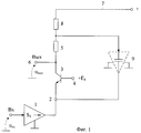
Наиболее близким по технической сущности к заявляемому устройству является КУ фиг.1 по патенту RU 2421878.The closest in technical essence to the claimed device is KU figure 1 according to patent RU 2421878.
Существенный недостаток известного КУ, архитектура которого присутствует также во многих других каскодных усилителях [1-19], состоит в том, что при ограничениях на напряжение питания (Еп), характерных для SiGe технологических процессов (Еп≤2,0÷2,5 В), его коэффициент усиления по напряжению (K0) получается сравнительно небольшим (K0mах=40÷50 дБ). В первую очередь это обусловлено неполной собственной компенсацией сопротивления резисторов коллекторной нагрузки, которые из-за малых Eп не могут выбираться высокоомными.A significant drawback of the well-known KU, the architecture of which is also present in many other cascode amplifiers [1-19], is that under restrictions on the supply voltage (E p ) characteristic of SiGe technological processes (E p ≤2.0 ÷ 2, 5 V), its voltage gain (K 0 ) turns out to be relatively small (K 0max = 40 ÷ 50 dB). This is primarily due to incomplete self-compensation of the resistance of the collector load resistors, which, due to low E p, cannot be selected as high-resistance.
Основная задача предлагаемого изобретения состоит в повышении коэффициента усиления по напряжению на 20÷30 дБ (до уровня 70-80 дБ). Это позволяет в ряде случаев исключить дополнительные каскады усиления, уменьшить общее энергопотребление в сравнении с многокаскадными усилителями.The main objective of the invention is to increase the voltage gain by 20 ÷ 30 dB (up to the level of 70-80 dB). This allows in some cases to exclude additional amplification stages, to reduce the overall power consumption in comparison with multi-stage amplifiers.
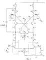
Поставленная задача решается тем, что в каскодном усилителе фиг.1, содержащем первый 1 входной преобразователь напряжение-ток, токовый выход 2 которого соединен с эмиттером первого 3 выходного транзистора, цепь установления статического режима 4, связанную с базой первого 3 выходного транзистора, первый 5 двухполюсник коллекторной нагрузки, первый вывод которого соединен с коллектором первого 3 выходного транзистора и выходом устройства 6, первую 7 шину источника питания, связанную с первым выводом второго 8 двухполюсника коллекторной нагрузки, второй вывод второго 8 двухполюсника коллекторной нагрузки и второй вывод первого 5 двухполюсника коллекторной нагрузки соединены друг с другом и связаны с эмиттером первого 3 выходного транзистора через неинвертирующую согласующую цепь 9 с коэффициентами передачи по току меньше единицы, предусмотрены новые элементы и связи - эмиттер первого 3 выходного транзистора соединен с базой второго 10 выходного транзистора, коллектор которого связан с первой 7 шиной источника питания, эмиттер связан со второй 11 шиной источника питания через первый токостабилизирующий источник 12 и подключен к эмиттеру третьего 13 выходного транзистора, коллектор третьего 13 выходного транзистора соединен с коллектором первого 3 выходного транзистора, база соединена с эмиттером четвертого 14 выходного транзистора и через второй токостабилизирующий источник 15 связана со второй 11 шиной источника питания, причем база четвертого 14 выходного транзистора подключена к базе первого 3 выходного транзистора, а его коллектор связан с коллектором второго 10 выходного транзистора.The problem is solved in that in the cascode amplifier of figure 1, containing the first 1 input voltage-current converter, the
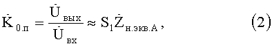
Схема усилителя-прототипа показана на чертеже фиг.1 для случая, когда в качестве неинвертирующей согласующей цепи 9 с коэффициентом передачи по току меньше единицы используется пассивный двухполюсник - разделительный конденсатор. На чертеже фиг.2 представлена схема заявляемого устройства в соответствии с п.1 и п.2 формулы изобретения.The amplifier circuit of the prototype is shown in FIG. 1 for the case when a passive bipolar isolating capacitor is used as a
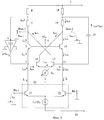
На чертеже фиг.3 показана схема заявляемого устройства в соответствии с п.3 формулы изобретения.The drawing of figure 3 shows a diagram of the inventive device in accordance with
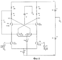
На чертежах фиг.4 и фиг.5 показаны схемы заявляемого устройства в соответствии с п.4 формулы изобретения.The drawings of figure 4 and figure 5 shows a diagram of the inventive device in accordance with
На чертеже фиг.6 приведена схема КУ фиг.3 в среде компьютерного моделирования PSpice на моделях интегральных транзисторов ФГУП НПП «Пульсар».The drawing of Fig.6 shows a diagram of the control unit of Fig.3 in a computer simulation environment PSpice on models of integrated transistors of FSUE NPP Pulsar.
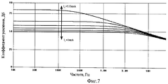
На чертеже фиг.7 представлена амплитудно-частотная характеристика коэффициента усиления по напряжению КУ фиг.6 при изменении тока первого токостабилизирующего двухполюсника I1 (I12, фиг.3) в пределах I1=0…530 мкА с шагом 106 мкА.The drawing of Fig.7 shows the amplitude-frequency characteristic of the voltage gain KU of Fig.6 when the current of the first current-stabilizing two-terminal I 1 (I 12 , Fig.3) changes within I 1 = 0 ... 530 μA with a step of 106 μA.
На чертеже фиг.8 показана схема КУ фиг.5, в которой выходной каскод реализован на p-n-p транзисторах.The drawing of Fig. 8 shows a diagram of the KU of Fig. 5, in which the output cascode is implemented on p-n-p transistors.
На чертеже фиг.9 приведена схема КУ фиг.8 в среде PSpice на моделях интегральных транзисторов ФГУП НПП «Пульсар» (npn TN15S, pnp TP15S).The drawing of Fig.9 shows a diagram of the KU of Fig.8 in the PSpice environment on models of integrated transistors of the Federal State Unitary Enterprise NPP Pulsar (npn TN15S, pnp TP15S).
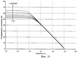
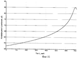
На чертеже фиг.10 представлена амплитудно-частотная характеристика КУ фиг.9, а на чертеже фиг.11 - зависимость коэффициента усиления по напряжению КУ фиг.9 от тока двухполюсника I1, соответствующего на чертеже фиг.2 - фиг.3 току первого токостабилизирующего двухполюсника 12 (I1=I12).In the drawing of Fig. 10, the amplitude-frequency characteristic of the KU of Fig. 9 is shown, and in the Fig. 11 is the dependence of the voltage gain of the KU of Fig. 9 on the current of the two-terminal I 1 corresponding in the drawing of Fig. 2 - Fig. 3 to the current of the first current-stabilizing bipolar 12 (I 1 = I 12 ).
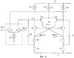
Каскодный усилитель фиг.2 содержит первый 1 входной преобразователь напряжение-ток, токовый выход 2 которого соединен с эмиттером первого 3 выходного транзистора, цепь установления статического режима 4, связанную с базой первого 3 выходного транзистора, первый 5 двухполюсник коллекторной нагрузки, первый вывод которого соединен с коллектором первого 3 выходного транзистора и выходом устройства 6, первую 7 шину источника питания, связанную с первым выводом второго 8 двухполюсника коллекторной нагрузки, второй вывод второго 8 двухполюсника коллекторной нагрузки и второй вывод первого 5 двухполюсника коллекторной нагрузки соединены друг с другом и связаны с эмиттером первого 3 выходного транзистора через неинвертирующую согласующую цепь 9 с коэффициентами передачи по току меньше единицы. Эмиттер первого 3 выходного транзистора соединен с базой второго 10 выходного транзистора, коллектор которого связан с первой 7 шиной источника питания, эмиттер связан со второй 11 шиной источника питания через первый токостабилизирующий источник 12 и подключен к эмиттеру третьего 13 выходного транзистора, коллектор третьего 13 выходного транзистора соединен с коллектором первого 3 выходного транзистора, база соединена с эмиттером четвертого 14 выходного транзистора и через второй токостабилизирующий источник 15 связана со второй 11 шиной источника питания, причем база четвертого 14 выходного транзистора подключена к базе первого 3 выходного транзистора, а его коллектор связан с коллектором второго 10 выходного транзистора.The cascode amplifier of FIG. 2 contains a first 1 voltage-current input converter, the
Кроме этого, на чертеже фиг.2, в соответствии с п.2 формулы изобретения, в качестве неинвертирующей согласующей цепи 9 с коэффициентами передачи по току меньше единицы используется разделительный конденсатор.In addition, in the drawing of figure 2, in accordance with
На чертеже фиг.3, в соответствии с п.3 формулы изобретения, в качестве второго токостабилизирующего источника 15 используется токовый выход второго 16 входного преобразователя «напряжение-ток».In the drawing of figure 3, in accordance with
В частном случае статический режим входных преобразователей 1 и 16 может устанавливаться источником опорного тока 17. Для симметрирования напряжений коллектор-база транзисторов 3 и 14 в частном случае могут использоваться резисторы 18 и 19.In the particular case, the static mode of the
На чертеже фиг.4, в соответствии с п.4 формулы изобретения, в качестве первого 1 и второго 16 входных преобразователей «напряжение-ток» используется дифференциальный каскад 20 с противофазными токовыми выходами, реализованный на транзисторах 21 и 22 и источнике тока 23.In the drawing of FIG. 4, in accordance with
На чертеже фиг.5 представлена схема фиг.4 для случая, когда в нее введен конденсатор 24, что позволяет обеспечить симметричный (парафазный) выход каскодного усилителя.The drawing of Fig. 5 shows a diagram of Fig. 4 for the case when a
Рассмотрим работу КУ фиг.2.Consider the work of KU figure 2.
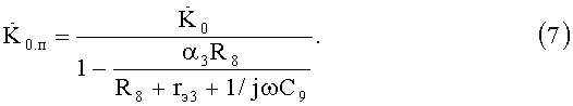
Предельный коэффициент усиления по напряжению КУ фиг.1 при нулевой емкости разделительного конденсатора 9 (C9=0) определяется сопротивлением R5 первого 5 двухполюсника коллекторной нагрузки:The limiting voltage gain KU of Fig. 1 at zero capacitance of the isolation capacitor 9 (C 9 = 0) is determined by the resistance R 5 of the first 5 two-terminal collector load:
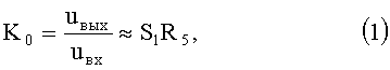
где R5>>R8;where R 5 >> R 8 ;
S1≈(rэ1)-1 - крутизна усиления входного преобразователя «напряжение-ток» в режиме короткого замыкания по выходу, зависящая в частном случае от сопротивления эмиттерного перехода (rэвх) входного транзистора данного преобразователя.S 1 ≈ (r e1 ) -1 is the gain slope of the input voltage-current converter in the output short circuit, which in a particular case depends on the resistance of the emitter junction (r evh ) of the input transistor of this converter.
Покажем аналитически, что более высокие значения K0 в диапазоне средних частот реализуются в схеме фиг.2 при токе I12=0 и C9≠0, что соответствует прототипу фиг.1, а еще более высокий K0 имеет заявляемая схема фиг.2 при токе первого 12 токостабилизирующего двухполюсника, лежащем в пределах I12=100÷150 мкА.Let us show analytically that higher values of K 0 in the mid-frequency range are realized in the circuit of FIG. 2 at a current of I 12 = 0 and C 9 ≠ 0, which corresponds to the prototype of FIG. 1, and the claimed circuit of FIG. 2 has an even higher K 0 at a current of the first 12 current-stabilizing two-terminal network, which lies within I 12 = 100 ÷ 150 μA.
Действительно, в общем случае комплексный коэффициент передачи по напряжению КУ фиг.2 при I12=0 и С9≠0 определяется по формуле:Indeed, in the General case, the complex transmission coefficient of voltage KU figure 2 when I 12 = 0 and C 9 ≠ 0 is determined by the formula:
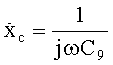
где ![]()
![]()
Если емкость конденсатора 9 равна нулю, то для КУ фиг.2 при условии, что R5>>R8 получаем формулу (1):If the capacitance of the
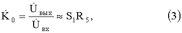
где R5>>R8 - сопротивления первого 5 и второго 8 двухполюсников коллекторной нагрузки.where R 5 >> R 8 are the resistances of the first 5 and second 8 two-terminal collector loads.
То есть (3) - это формула для K0 усилителя-прототипа при условии, что C9=0.That is, (3) is the formula for K 0 of the prototype amplifier, provided that C 9 = 0.
Комплекс эквивалентной нагрузки в узле А КУ фиг.2 при C9≠O и токе I12=0, то есть когда транзисторы 10, 13 обесточены и не влияют на работу схемы, можно найти по формуле:The equivalent load complex in the node A of KU of figure 2 at C 9 ≠ O and current I 12 = 0, that is, when the
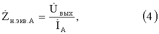
где 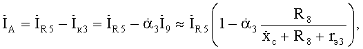
![]()
![]()
![]()
![]()
![]()
![]()

После преобразований последней формулы находим, чтоAfter transformations of the last formula, we find that
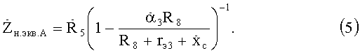
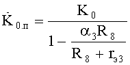
Поэтому коэффициент усиления по напряжению КУ фиг.2 при токе I12=0 и C9≠0Therefore, the voltage gain KU of figure 2 at a current of I 12 = 0 and C 9 ≠ 0
При ![]()
![]()
В области рабочих частот, когда 1/ωC9<<rэ3, коэффициент К0.п не лучше, чемIn the field of operating frequencies, when 1 / ωC 9 << r e3 , the coefficient K 0.n is not better than
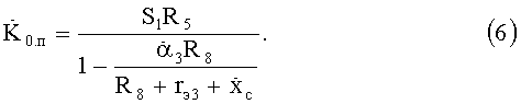
Выигрыш по K0, который дает схема КУ фиг.2 при токе I12=0 в сравнении со случаем, когда в схеме фиг.2 I12=0, C9=0, можно оценить с помощью специального комплексного коэффициентаThe gain in K 0 , which gives the scheme KU of figure 2 at a current of I 12 = 0 in comparison with the case when in the scheme of figure 2 I 12 = 0, C 9 = 0, can be estimated using a special complex coefficient
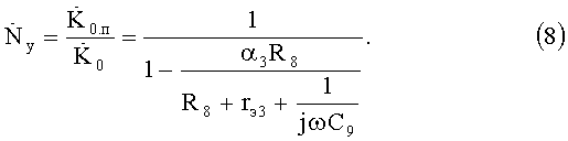
Если ω=0, то ![]()
![]()
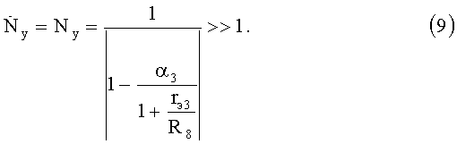
В лучшем случае при R8>>rэ3 In the best case, when R 8 >> r e3
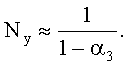
Однако с учетом реальных значений параметров элементов знаменатель формулы (9) достаточно существенно отличается от нуля, что не позволяет реализовать в КУ-прототипе предельные значения Nу и, как следствие, коэффициента усиления по напряжению.However, taking into account the real values of the parameters of the elements, the denominator of formula (9) is quite significantly different from zero, which does not allow the KU prototype to implement the limiting values of N y and, as a result, the voltage gain.
В схеме КУ фиг.2, которая является развитием схемы фиг.1, на передачу тока i9 в узел А оказывают влияние дополнительные элементы 10, 12, 13, 14, 15.In the KU circuit of FIG. 2, which is a development of the circuit of FIG. 1,
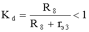
Можно показать, что эффективный коэффициент усиления по напряжению (K0.н) каскодного усилителя фиг.2 в области средних частот, когда влиянием сопротивления 1/С9ω можно пренебречь, а ток I12≠0, определяется по формулеIt can be shown that the effective voltage gain (K 0.n ) of the cascode amplifier of Fig. 2 in the middle frequency region, when the influence of
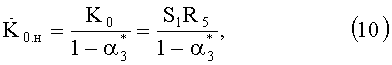
где 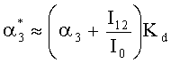
I0 - статический ток эмиттера транзисторов 3 и 14;I 0 is the static current of the emitter of
Таким образом, в заявленной схеме на коэффициент усиления по напряжению оказывает влияние ток первого 12 токостабилизирующего двухполюсника I12:Thus, in the claimed circuit, the current gain of the first 12 current-stabilizing two-terminal I 12 has an effect on the voltage gain:
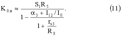
За счет выбора тока I12 в схеме фиг.2 можно обеспечить практически любое значение K0.н, что недостижимо в КУ-прототипе.By choosing the current I 12 in the circuit of figure 2, you can provide almost any value of K 0.n , which is unattainable in the KU prototype.
Так, например, для получения Nmax-кратного выигрыша по Kу необходимо обеспечить отношение токовSo, for example, to obtain N max -fold gain in K y, it is necessary to ensure the ratio of currents
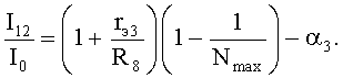
Как показывают графики фиг.11, при Nmax=10 численные значения тока I12≈600 мкА.As the graphs of Fig. 11 show, at N max = 10 the numerical values of the current I 12 ≈600 μA.
Данные теоретические выводы подтверждают результаты компьютерного моделирования фиг.7, фиг.10, фиг.11.These theoretical conclusions confirm the results of computer simulation of Fig.7, Fig.10, Fig.11.
Таким образом, заявляемое схемотехническое решение характеризуется более высокими значениями коэффициента усиления по напряжению.Thus, the claimed circuit solution is characterized by higher values of the voltage gain.
БИБЛИОГРАФИЧЕСКИЙ СПИСОКBIBLIOGRAPHIC LIST
1. Патент США №6825723 fig.3.1. US patent No. 6825723 fig.3.
2. Патент США №4151483 fig.2.2. US patent No. 4151483 fig.2.
3. Патент США №4151484.3. US patent No. 4151484.
4. Патент США №3882410 fig.3.4. US patent No. 3882410 fig. 3.
5. Патентная заявка WO 2004/030207.5. Patent application WO 2004/030207.
6. Патент США №4021749 fig.2.6. US patent No. 4021749 fig.2.
7. Патент США №3693108 fig.9.7. US Patent No. 3693108 fig. 9.
8. Патент США №7113043 fig.2.8. US patent No. 7113043 fig.2.
9. Патентная заявка США 2006/003 35 62.9. US Patent Application 2006/003 35 62.
10. Патентная заявка США 2006/0132242.10. US Patent Application 2006/0132242.
11. Патентная заявка США 2006/0119435.11. US patent application 2006/0119435.
12. Патентная заявка США 2005/0248408.12. US Patent Application 2005/0248408.
13. Патент США №6204728.13. US patent No. 6204728.
14. Патент США №6278329.14. US patent No. 6278329.
15. Патентная заявка США 2005/0225397.15. US patent application 2005/0225397.
16. Патент США №5451906.16. US Patent No. 5451906.
17. Патент США №7098743 fig.1.17. US Patent No. 7098743 fig. 1.
18. Патент Англии GB №1431481 fig.2.18. British Patent GB No. 1431481 fig. 2.
19. Патент США №6515547 fig.2.19. US patent No. 6515547 fig.2.
Claims (4)
Priority Applications (1)
| Application Number | Priority Date | Filing Date | Title |
|---|---|---|---|
| RU2011139549/08A RU2468503C1 (en) | 2011-09-28 | 2011-09-28 | Cascode amplifier |
Applications Claiming Priority (1)
| Application Number | Priority Date | Filing Date | Title |
|---|---|---|---|
| RU2011139549/08A RU2468503C1 (en) | 2011-09-28 | 2011-09-28 | Cascode amplifier |
Publications (1)
| Publication Number | Publication Date |
|---|---|
| RU2468503C1 true RU2468503C1 (en) | 2012-11-27 |
Family
ID=49255029
Family Applications (1)
| Application Number | Title | Priority Date | Filing Date |
|---|---|---|---|
| RU2011139549/08A RU2468503C1 (en) | 2011-09-28 | 2011-09-28 | Cascode amplifier |
Country Status (1)
| Country | Link |
|---|---|
| RU (1) | RU2468503C1 (en) |
Cited By (1)
| Publication number | Priority date | Publication date | Assignee | Title |
|---|---|---|---|---|
| RU2571369C1 (en) * | 2014-11-05 | 2015-12-20 | Федеральное Государственное Бюджетное Образовательное Учреждение Высшего Профессионального Образования "Донской Государственный Технический Университет" (Дгту) | Cascode amplifier with extended frequency band |
Citations (4)
| Publication number | Priority date | Publication date | Assignee | Title |
|---|---|---|---|---|
| US6924701B1 (en) * | 2002-09-03 | 2005-08-02 | Ikanos Communications, Inc. | Method and apparatus for compensating an amplifier |
| US20100007419A1 (en) * | 2008-07-09 | 2010-01-14 | Analog Devices, Inc. | Instrumentation Input Systems |
| RU2411636C1 (en) * | 2009-08-03 | 2011-02-10 | Государственное образовательное учреждение высшего профессионального образования "Южно-Российский государственный университет экономики и сервиса" (ГОУ ВПО "ЮРГУЭС") | Cascode differential amplifier with low voltage of zero shift |
| RU2428786C1 (en) * | 2010-05-24 | 2011-09-10 | Государственное образовательное учреждение высшего профессионального образования "Южно-Российский государственный университет экономики и сервиса" (ГОУ ВПО "ЮРГУЭС") | Cascode amplifier |
-
2011
- 2011-09-28 RU RU2011139549/08A patent/RU2468503C1/en not_active IP Right Cessation
Patent Citations (4)
| Publication number | Priority date | Publication date | Assignee | Title |
|---|---|---|---|---|
| US6924701B1 (en) * | 2002-09-03 | 2005-08-02 | Ikanos Communications, Inc. | Method and apparatus for compensating an amplifier |
| US20100007419A1 (en) * | 2008-07-09 | 2010-01-14 | Analog Devices, Inc. | Instrumentation Input Systems |
| RU2411636C1 (en) * | 2009-08-03 | 2011-02-10 | Государственное образовательное учреждение высшего профессионального образования "Южно-Российский государственный университет экономики и сервиса" (ГОУ ВПО "ЮРГУЭС") | Cascode differential amplifier with low voltage of zero shift |
| RU2428786C1 (en) * | 2010-05-24 | 2011-09-10 | Государственное образовательное учреждение высшего профессионального образования "Южно-Российский государственный университет экономики и сервиса" (ГОУ ВПО "ЮРГУЭС") | Cascode amplifier |
Cited By (1)
| Publication number | Priority date | Publication date | Assignee | Title |
|---|---|---|---|---|
| RU2571369C1 (en) * | 2014-11-05 | 2015-12-20 | Федеральное Государственное Бюджетное Образовательное Учреждение Высшего Профессионального Образования "Донской Государственный Технический Университет" (Дгту) | Cascode amplifier with extended frequency band |
Similar Documents
| Publication | Publication Date | Title |
|---|---|---|
| RU2432669C1 (en) | Broadband amplifier | |
| RU2428786C1 (en) | Cascode amplifier | |
| RU2421879C1 (en) | Differential amplifier with high-frequency compensation | |
| RU2421880C1 (en) | Broadband amplifier | |
| RU2427071C1 (en) | Broadband amplifier | |
| RU2468503C1 (en) | Cascode amplifier | |
| RU2380824C1 (en) | Alternating current amplifier with controlled amplification | |
| RU2413355C1 (en) | Differential amplifier with paraphase output | |
| RU2416146C1 (en) | Differential amplifier with increased amplification factor | |
| RU2536672C1 (en) | Low-output capacitance composite transistor | |
| RU2374757C1 (en) | Cascode differential amplifier | |
| RU2421888C1 (en) | Differential amplifier | |
| RU2422981C1 (en) | Differential ac amplifier | |
| RU2390912C2 (en) | Cascode differential amplifier | |
| RU2475941C1 (en) | Differential amplifier with complementary input cascade | |
| RU2439780C1 (en) | Cascode differential amplifier | |
| RU2390911C2 (en) | Cascode differential amplifier | |
| RU2421882C1 (en) | Two-cascade hf-amplifier | |
| RU2423778C1 (en) | High-frequency compensation cascode differential amplifier | |
| RU2319292C1 (en) | Cascode differential amplifier | |
| RU2463703C1 (en) | Cascode differential amplifier | |
| RU2420864C1 (en) | Differential amplifier with high amplification ratio | |
| RU2420861C1 (en) | Differential amplifier with high amplification ratio by voltage | |
| RU2421881C1 (en) | Differential amplifier | |
| RU2432668C1 (en) | Differential operational amplifier with paraphase output |
Legal Events
| Date | Code | Title | Description |
|---|---|---|---|
| MM4A | The patent is invalid due to non-payment of fees |
Effective date: 20130929 |