RU2379861C2 - Multi-layer element with zones of varying microstructure incorporating conducting coating - Google Patents
Multi-layer element with zones of varying microstructure incorporating conducting coating Download PDFInfo
- Publication number
- RU2379861C2 RU2379861C2 RU2007111712/09A RU2007111712A RU2379861C2 RU 2379861 C2 RU2379861 C2 RU 2379861C2 RU 2007111712/09 A RU2007111712/09 A RU 2007111712/09A RU 2007111712 A RU2007111712 A RU 2007111712A RU 2379861 C2 RU2379861 C2 RU 2379861C2
- Authority
- RU
- Russia
- Prior art keywords
- relief structure
- multilayer element
- coating
- depth
- layer
- Prior art date
Links
Images
Classifications
-
- B—PERFORMING OPERATIONS; TRANSPORTING
- B32—LAYERED PRODUCTS
- B32B—LAYERED PRODUCTS, i.e. PRODUCTS BUILT-UP OF STRATA OF FLAT OR NON-FLAT, e.g. CELLULAR OR HONEYCOMB, FORM
- B32B27/00—Layered products comprising a layer of synthetic resin
-
- H—ELECTRICITY
- H05—ELECTRIC TECHNIQUES NOT OTHERWISE PROVIDED FOR
- H05K—PRINTED CIRCUITS; CASINGS OR CONSTRUCTIONAL DETAILS OF ELECTRIC APPARATUS; MANUFACTURE OF ASSEMBLAGES OF ELECTRICAL COMPONENTS
- H05K3/00—Apparatus or processes for manufacturing printed circuits
- H05K3/10—Apparatus or processes for manufacturing printed circuits in which conductive material is applied to the insulating support in such a manner as to form the desired conductive pattern
- H05K3/14—Apparatus or processes for manufacturing printed circuits in which conductive material is applied to the insulating support in such a manner as to form the desired conductive pattern using spraying techniques to apply the conductive material, e.g. vapour evaporation
-
- B—PERFORMING OPERATIONS; TRANSPORTING
- B42—BOOKBINDING; ALBUMS; FILES; SPECIAL PRINTED MATTER
- B42D—BOOKS; BOOK COVERS; LOOSE LEAVES; PRINTED MATTER CHARACTERISED BY IDENTIFICATION OR SECURITY FEATURES; PRINTED MATTER OF SPECIAL FORMAT OR STYLE NOT OTHERWISE PROVIDED FOR; DEVICES FOR USE THEREWITH AND NOT OTHERWISE PROVIDED FOR; MOVABLE-STRIP WRITING OR READING APPARATUS
- B42D25/00—Information-bearing cards or sheet-like structures characterised by identification or security features; Manufacture thereof
- B42D25/30—Identification or security features, e.g. for preventing forgery
- B42D25/328—Diffraction gratings; Holograms
-
- G—PHYSICS
- G02—OPTICS
- G02B—OPTICAL ELEMENTS, SYSTEMS OR APPARATUS
- G02B5/00—Optical elements other than lenses
- G02B5/18—Diffraction gratings
- G02B5/1847—Manufacturing methods
- G02B5/1857—Manufacturing methods using exposure or etching means, e.g. holography, photolithography, exposure to electron or ion beams
-
- G—PHYSICS
- G02—OPTICS
- G02B—OPTICAL ELEMENTS, SYSTEMS OR APPARATUS
- G02B5/00—Optical elements other than lenses
- G02B5/30—Polarising elements
-
- G—PHYSICS
- G06—COMPUTING; CALCULATING OR COUNTING
- G06K—GRAPHICAL DATA READING; PRESENTATION OF DATA; RECORD CARRIERS; HANDLING RECORD CARRIERS
- G06K19/00—Record carriers for use with machines and with at least a part designed to carry digital markings
- G06K19/06—Record carriers for use with machines and with at least a part designed to carry digital markings characterised by the kind of the digital marking, e.g. shape, nature, code
- G06K19/067—Record carriers with conductive marks, printed circuits or semiconductor circuit elements, e.g. credit or identity cards also with resonating or responding marks without active components
- G06K19/07—Record carriers with conductive marks, printed circuits or semiconductor circuit elements, e.g. credit or identity cards also with resonating or responding marks without active components with integrated circuit chips
-
- H—ELECTRICITY
- H05—ELECTRIC TECHNIQUES NOT OTHERWISE PROVIDED FOR
- H05K—PRINTED CIRCUITS; CASINGS OR CONSTRUCTIONAL DETAILS OF ELECTRIC APPARATUS; MANUFACTURE OF ASSEMBLAGES OF ELECTRICAL COMPONENTS
- H05K3/00—Apparatus or processes for manufacturing printed circuits
- H05K3/10—Apparatus or processes for manufacturing printed circuits in which conductive material is applied to the insulating support in such a manner as to form the desired conductive pattern
- H05K3/12—Apparatus or processes for manufacturing printed circuits in which conductive material is applied to the insulating support in such a manner as to form the desired conductive pattern using thick film techniques, e.g. printing techniques to apply the conductive material or similar techniques for applying conductive paste or ink patterns
-
- H—ELECTRICITY
- H05—ELECTRIC TECHNIQUES NOT OTHERWISE PROVIDED FOR
- H05K—PRINTED CIRCUITS; CASINGS OR CONSTRUCTIONAL DETAILS OF ELECTRIC APPARATUS; MANUFACTURE OF ASSEMBLAGES OF ELECTRICAL COMPONENTS
- H05K2201/00—Indexing scheme relating to printed circuits covered by H05K1/00
- H05K2201/09—Shape and layout
- H05K2201/09009—Substrate related
- H05K2201/09036—Recesses or grooves in insulating substrate
-
- H—ELECTRICITY
- H05—ELECTRIC TECHNIQUES NOT OTHERWISE PROVIDED FOR
- H05K—PRINTED CIRCUITS; CASINGS OR CONSTRUCTIONAL DETAILS OF ELECTRIC APPARATUS; MANUFACTURE OF ASSEMBLAGES OF ELECTRICAL COMPONENTS
- H05K2201/00—Indexing scheme relating to printed circuits covered by H05K1/00
- H05K2201/09—Shape and layout
- H05K2201/09009—Substrate related
- H05K2201/09045—Locally raised area or protrusion of insulating substrate
-
- Y—GENERAL TAGGING OF NEW TECHNOLOGICAL DEVELOPMENTS; GENERAL TAGGING OF CROSS-SECTIONAL TECHNOLOGIES SPANNING OVER SEVERAL SECTIONS OF THE IPC; TECHNICAL SUBJECTS COVERED BY FORMER USPC CROSS-REFERENCE ART COLLECTIONS [XRACs] AND DIGESTS
- Y10—TECHNICAL SUBJECTS COVERED BY FORMER USPC
- Y10T—TECHNICAL SUBJECTS COVERED BY FORMER US CLASSIFICATION
- Y10T428/00—Stock material or miscellaneous articles
- Y10T428/24—Structurally defined web or sheet [e.g., overall dimension, etc.]
- Y10T428/24479—Structurally defined web or sheet [e.g., overall dimension, etc.] including variation in thickness
- Y10T428/2457—Parallel ribs and/or grooves
Landscapes
- Engineering & Computer Science (AREA)
- Physics & Mathematics (AREA)
- Manufacturing & Machinery (AREA)
- Microelectronics & Electronic Packaging (AREA)
- General Physics & Mathematics (AREA)
- Optics & Photonics (AREA)
- Computer Hardware Design (AREA)
- Theoretical Computer Science (AREA)
- Laminated Bodies (AREA)
- Shielding Devices Or Components To Electric Or Magnetic Fields (AREA)
- Materials For Medical Uses (AREA)
- Prostheses (AREA)
Abstract
Description
Область техникиTechnical field
Настоящее изобретение относится к многослойному элементу, имеющему реплицируемый лаковый слой, в котором сформирована рельефная структура и который снабжен электропроводящим покрытием.The present invention relates to a multilayer element having a replicable varnish layer in which a relief structure is formed and which is provided with an electrically conductive coating.
Уровень техникиState of the art
Многослойные элементы в форме пленочных элементов используются во многих областях, например, в качестве защитных элементов для получения оптического эффекта. Они используются также в качестве части электрической схемы, или они сами образуют электрическую схему, например переключающую схему. Такие переключающие схемы используются, например, в так называемых RFID-этикетках (этикетках с радиочастотной идентификацией), т.е. в этикетках для идентификации товаров с помощью радиочастот (RF). Под радиочастотной идентификацией следует понимать в общем бесконтактную RF-коммуникацию между преобразователем, который ассоциирован с предметом или личностью, и считывающим устройством. Преобразователь при этом имеет, например, антенну, которая является частью контура переключения частоты, и/или связан с полупроводниковым чипом.Multilayer elements in the form of film elements are used in many fields, for example, as protective elements for obtaining an optical effect. They are also used as part of an electrical circuit, or they themselves form an electrical circuit, for example a switching circuit. Such switching circuits are used, for example, in the so-called RFID labels (RFID tags), i.e. on labels for identifying goods using radio frequencies (RF). Radio frequency identification is understood to mean generally contactless RF communication between a transducer that is associated with an object or person and a reader. In this case, the converter has, for example, an antenna, which is part of the frequency switching loop, and / or connected to a semiconductor chip.
Для такого использования электрически проводящие структуры следует изготавливать на пленочном элементе или в пленочном элементе, причем эти структуры имеют очень незначительные размеры. Для этого следует осуществлять различные операции, которые требуют больших затрат труда и времени изготовления, являются вредными для окружающей среды или снижают качество, как, например, получение электропроводящих слоев травлением. При травлении можно, например, внести загрязнения в расположенный под проводящими структурами слой полупроводника, причем уже самые малые количества посторонних атомов могут являться значительным источником помех.For such use, electrically conductive structures should be made on the film element or in the film element, and these structures are very small. For this, various operations should be carried out that require large labor costs and manufacturing time, are harmful to the environment or reduce quality, such as, for example, the production of electrically conductive layers by etching. During etching, it is possible, for example, to introduce contaminants into the semiconductor layer located under the conductive structures, and even the smallest amounts of foreign atoms can be a significant source of interference.
Из-за слоистой структуры переключающих схем требуется проведение множества циклов таких технологических операций, так что потребуются дальнейшие затраты на изготовление с точной подгонкой.Due to the layered structure of the switching circuits, many cycles of such technological operations are required, so that further manufacturing costs with a precise fit are required.
Существо изобретенияSUMMARY OF THE INVENTION
Технической задачей настоящего изобретения является устранение указанных недостатков и создание многослойного элемента со структурированными электропроводящими покрытиями, которые можно изготовлять с небольшими затратами, высокой точностью и высоким разрешением.The technical task of the present invention is to remedy these disadvantages and create a multilayer element with structured conductive coatings that can be manufactured with low cost, high accuracy and high resolution.
Поставленная задача согласно изобретению решена путем создания многослойного элемента с реплицируемым лаковым слоем, причем первая рельефная структура сформирована в реплицируемом лаковом слое в плоскости, определяемой осями координат x и y, в первой области многослойного элемента, при этом на реплицируемый лаковый слой в первой области многослойного элемента и в прилегающей второй области многослойного элемента нанесено электропроводящее покрытие с постоянной плотностью поверхности. Первая рельефная структура является структурой с высоким значением отношения глубины к ширине отдельных структурных элементов, в частности со значением отношения глубины к ширине >2, и образована, по меньшей мере, одной вертикальной или почти вертикальной боковой гранью, проходящей по всей или по значительной части глубины рельефной структуры, при этом на вертикальной или почти вертикальной боковой грани первой рельефной структуры имеются участки, на которые не осаждено проводящее покрытие, нанесенное на первую рельефную структуру, или осаждено слоем очень малой толщины, так что электропроводность покрытия в области боковых граней является значительно более низкой. Поставленная задача решена также путем создания способа изготовления многослойного элемента, заключающегося в том, что в реплицируемом лаковом слое многослойного элемента формируют первую рельефную структуру в первой области многослойного элемента и затем наносят на реплицируемый слой в первой области многослойного элемента и в прилегающей второй области многослойного элемента электропроводящее покрытие с постоянной плотностью по поверхности. Первую рельефную структуру формируют с высоким значением отношения глубины к ширине отдельных структурных элементов, в частности со значением отношения глубины к ширине >2, и, по меньшей мере, с одной вертикальной или почти вертикальной боковой гранью, при этом на вертикальных или почти вертикальных боковых гранях первой рельефной структуры формируют области, на которые не осаждают проводящее покрытие, нанесенное на первую рельефную структуру, или осаждают слоем малой толщины, так что электропроводность покрытия в области боковых граней является значительно более низкой.The problem according to the invention is solved by creating a multilayer element with a replicated varnish layer, the first relief structure being formed in the replicated varnish layer in the plane defined by the x and y coordinate axes in the first region of the multilayer element, with the replicated varnish layer in the first region of the multilayer element and in the adjacent second region of the multilayer element, an electrically conductive coating with a constant surface density is applied. The first relief structure is a structure with a high value of the ratio of depth to width of individual structural elements, in particular with a value of the ratio of depth to width> 2, and is formed by at least one vertical or almost vertical side face that runs along all or a significant part of the depth relief structure, while on the vertical or almost vertical lateral face of the first relief structure there are areas on which a conductive coating deposited on the first relief structure is not deposited, or deposited by a layer of very small thickness, so that the conductivity of the coating in the region of the side faces is significantly lower. The problem is also solved by creating a method of manufacturing a multilayer element, which consists in the fact that the first relief structure is formed in the replicated varnish layer of the multilayer element in the first region of the multilayer element and then applied to the replicated layer in the first region of the multilayer element and in the adjacent second region of the multilayer element coating with constant surface density. The first relief structure is formed with a high value of the ratio of depth to width of individual structural elements, in particular with a value of the ratio of depth to width> 2, and at least one vertical or almost vertical side face, while on vertical or almost vertical side faces areas of the first relief structure that the conductive coating deposited on the first relief structure is not deposited on or deposited with a layer of small thickness, so that the electrical conductivity of the coating in the side face It is much lower.
Благодаря тому что первая рельефная структура образована с таким высоким значением отношения глубины к ширине и, по меньшей мере, с одной вертикальной или почти вертикальной боковой гранью, на боковых гранях рельефной структуры получаются области, на которые не осаждается нанесенное на рельефную структуру электропроводящее покрытие или осаждается слой очень малой толщины, так что электропроводность покрытия в области боковых граней оказывается значительно более низкой или покрытие там полностью прерывается. Особым преимуществом при этом является достигаемое высокое разрешение, т.е. возможно образование очень тонких проводящих структур, которые не могут осуществляться с помощью оптического способа экспонирования с последующим травлением. Кроме того, возможно точно устанавливать поверхностное сопротивление электропроводящих областей и кодировать информацию в защитном элементе, которую можно считывать.Due to the fact that the first relief structure is formed with such a high ratio of depth to width and with at least one vertical or almost vertical side face, on the side faces of the relief structure, areas are obtained on which the electrically conductive coating deposited on the relief structure does not deposit or is deposited the layer is very small in thickness, so that the electrical conductivity of the coating in the region of the side faces is much lower or the coating is completely interrupted there. A particular advantage is the achieved high resolution, i.e. the formation of very thin conductive structures that cannot be carried out using the optical exposure method with subsequent etching is possible. In addition, it is possible to precisely set the surface resistance of the electrically conductive regions and encode information in the security element that can be read.
Безразмерное значение отношения глубины к ширине является отличительным признаком для характеристики структур, в частности микроструктур. Предпочтительно его используют, чтобы описать периодические структуры, например, с пилообразным ходом. В качестве глубины обозначается расстояние между самой высокой и самой низкой следующими друг за другом точками структуры, т.е. речь идет о расстоянии между «вершиной» и «впадиной». В качестве ширины обозначается расстояние между соседними самыми высокими точками, т.е. между двумя «вершинами» (период). Чем выше значение отношения глубины к ширине, тем более крутыми выполнены «боковые грани вершин». Модель описания можно применить также к непериодическим структурам. Например, речь может идти о дискретно распределенных линейных областях, которые образованы лишь в виде «впадины», причем расстояние между двумя «впадинами» во много раз выше, чем глубина «впадин». При формальном применении указанного выше определения рассчитанное таким образом значение отношения глубины к ширине было бы равно приблизительно нулю и не воспроизводило бы характерные физические свойства. Поэтому при дискретно расположенных структурах, которые состоят в основном из «впадины», в значении отношения следует указать отношение глубины «впадины» к ширине «впадины».The dimensionless value of the ratio of depth to width is a hallmark for characterizing structures, in particular microstructures. Preferably, it is used to describe periodic structures, for example, with a sawtooth course. The depth is the distance between the highest and lowest successive points of the structure, i.e. we are talking about the distance between the "peak" and the "hollow". The width is the distance between the adjacent highest points, i.e. between two "peaks" (period). The higher the value of the ratio of depth to width, the more abrupt the “side faces of the vertices” are made. The description model can also be applied to non-periodic structures. For example, we can talk about discretely distributed linear regions that are formed only in the form of a “depression”, and the distance between two “depressions” is many times higher than the depth of the “depressions”. With the formal application of the above definition, the value of the ratio of depth to width calculated in this way would be approximately zero and would not reproduce the characteristic physical properties. Therefore, with discretely located structures, which consist mainly of a “trough”, the ratio of the depth of the “trough” to the width of the “trough” should be indicated in the ratio value.
Несмотря на приведенные выше преимущества способ изготовления согласно изобретению является экономичным, поскольку он исключает дорогостоящие технологические операции для формирования проводящих линий.Despite the above advantages, the manufacturing method according to the invention is economical since it eliminates the costly processing steps for forming conductive lines.
Предусмотрено, что первая рельефная структура образована в виде функции координат x и/или y, которая периодически изменяет глубину первой рельефной структуры в направлении x и/или в направлении y. При этом предпочтительными являются функции, которые обеспечивают формирование, по меньшей мере, вертикальных боковых граней. Предпочтительны пилообразные функции и прямоугольные функции. Таким образом, образованы вертикальные боковые грани с острыми кромками, так что проводящее покрытие прервано по определенному контуру вдоль кромок. Покрытие на первой рельефной структуре в направлении, вертикальном кромкам, является неэлектропроводным или имеет очень высокое электрическое сопротивление.It is envisaged that the first relief structure is formed as a function of the x and / or y coordinates, which periodically changes the depth of the first relief structure in the x direction and / or in the y direction. Preferred are functions that enable the formation of at least vertical side faces. Sawtooth functions and rectangular functions are preferred. Thus, vertical side faces with sharp edges are formed, so that the conductive coating is interrupted along a certain contour along the edges. The coating on the first relief structure in the direction vertical to the edges is non-conductive or has a very high electrical resistance.
Толщина t покрытия, которое осаждается на наклоненной под углом α относительно горизонтали скошенной боковой грани, определяется выражениемThe thickness t of the coating, which is deposited on an inclined lateral edge inclined at an angle α relative to the horizontal, is determined by the expression
t = t0 cos α,t = t 0 cos α,
где t0 является толщиной покрытия, осажденного на горизонтальную поверхность. Толщина t0 при этом устанавливается в зависимости от материала покрытия таким образом, что наклоненные боковые грани не «смазываются», т.е. там не осаждается никакого материала покрытия или имеется слой значительно более тонкий по сравнению с толщиной слоя плоской поверхности. С повышением толщины t0 в некоторых случаях покрытие может осаждаться также на вертикальных или почти вертикальных боковых гранях, например, если частицы материала покрытия движутся не по общей траектории полета потока частиц. Оптимальное значение можно определить предпочтительно с помощью ряда экспериментов. Оптимальноеwhere t 0 is the thickness of the coating deposited on a horizontal surface. The thickness t 0 is set depending on the coating material so that the inclined side faces are not “smeared”, i.e. no coating material is deposited there, or there is a layer significantly thinner than the thickness of the flat surface layer. With increasing thickness t 0 in some cases, the coating can also be deposited on vertical or almost vertical side faces, for example, if particles of the coating material do not move along the general path of the particle stream. The optimal value can be determined preferably using a series of experiments. Optimal
значение t0 ориентировано на то, чтобы на боковых гранях первой рельефной структуры получались области, на которых нанесенное на первую рельефную структуру проводящее покрытие не осаждалось или осаждалось столь малой толщины, что электропроводность покрытия в области боковых граней оказывалась значительно более низкой.the value of t 0 is oriented so that, on the side faces of the first relief structure, regions are obtained on which the conductive coating deposited on the first relief structure is not deposited or is so thin that the conductivity of the coating in the region of the side faces is much lower.
Толщина t0 неструктурированной области должна быть меньше 500 нм, предпочтительно меньше 50 нм. Оптимальную толщину t0 можно определить опытным путем, при этом можно также учесть влияние материала покрытия на электрические и другие свойства материала покрытия.The thickness t 0 of the unstructured region should be less than 500 nm, preferably less than 50 nm. The optimum thickness t 0 can be determined empirically, while the influence of the coating material on the electrical and other properties of the coating material can also be taken into account.
Если подлежащая покрытию рельефная структура имеет высокое значение отношения глубины к ширине, то выгодным образом увеличивается возможность образования на вертикальных или почти вертикальных боковых гранях первой рельефной структуры областей, на которых не осаждается электропроводящее покрытие, нанесенное на первую рельефную структуру, или осаждается лишь настольно малой толщиной слоя, что электрическая проводимость покрытия в области боковых граней является значительно более низкой. Предпочтительно можно предусмотреть, чтобы значение отношения глубины к ширине рельефной структуры было >2.If the relief structure to be coated has a high depth to width ratio, then the possibility of forming regions on which the electrically conductive coating deposited on the first relief structure does not deposit, or is deposited only in a tabletop thickness, is advantageously increased on the vertical or almost vertical side faces of the first relief structure. layer that the electrical conductivity of the coating in the region of the side faces is significantly lower. Preferably, it can be provided that the ratio of depth to width of the relief structure is> 2.
Как показали опыты, угол α наклона боковых граней по величине может отклоняться от вертикали примерно на 10°, не ставя под сомнение описанный эффект.As experiments have shown, the angle α of inclination of the side faces in magnitude can deviate from the vertical by about 10 °, without questioning the described effect.
Толщина t покрытия на боковых гранях устанавливается с помощью выбора угла α. При этом при угле α речь может идти также об угле наклона участка кривой, который может определяться первым ответвлением кривой.The thickness t of the coating on the side faces is set by choosing the angle α. Moreover, at an angle α, we can also speak about the angle of inclination of a portion of the curve, which can be determined by the first branch of the curve.
Если первая рельефная структура образована в виде функции одной координаты, то рельефную структуру очень просто выполнить. В частности, первая рельефная структура может быть дифракционной структурой с малым периодом решетки, например в диапазоне от 50 нм до 10 мкм. При такой рельефной структуре речь может идти о линейной дифракционной решетке.If the first relief structure is formed as a function of one coordinate, then the relief structure is very simple to perform. In particular, the first relief structure may be a diffraction structure with a short lattice period, for example in the range from 50 nm to 10 μm. With such a relief structure, we can talk about a linear diffraction grating.
Таким способом можно изготовить линейный поляризатор, образованный предпочтительно с длиной периода от 100 нм до 800 нм. Предпочтительно можно предусмотреть толщину покрытия t0<10 нм. Из-за высокого возможного разрешения первой рельефной структуры выполнение линейного поляризатора не ограничено выполнением для поляризации в одной плоскости колебаний. Скорее, может быть предусмотрено образование расположенных рядом друг с другом областей с различным направлением поляризации, причем области можно выполнить в качестве носителей информации. Например, области могут образовывать считываемый машинным способом штрихкод или в виде алфавитно-цифрового знака, или в форме видеоизображения. Эти области могут быть видимыми в поляризованном свете, например, если они ориентированы таким образом, что их плоскость поляризации направлена перпендикулярно к плоскости поляризации облучающего или проходящего насквозь света, благодаря чему они выделяются на фоне затемненными. Можно также предусмотреть «декодирующую» пленку, которая при освещении неполяризованным светом в сочетании с описанной выше структурой позволяет выявить скрытую информацию.In this way, a linear polarizer can be made, preferably formed with a period length from 100 nm to 800 nm. Preferably, a coating thickness of t 0 <10 nm can be provided. Due to the high possible resolution of the first relief structure, the implementation of a linear polarizer is not limited to the execution for polarization in one plane of oscillation. Rather, it can be envisaged the formation of adjacent adjacent to each other areas with different directions of polarization, and the area can be performed as storage media. For example, the regions may form a machine-readable barcode either in the form of an alphanumeric character or in the form of a video image. These areas can be visible in polarized light, for example, if they are oriented in such a way that their plane of polarization is directed perpendicular to the plane of polarization of the light irradiating or passing through, so that they stand out against the background darkened. You can also provide a "decoding" film, which when illuminated with unpolarized light in combination with the structure described above, reveals hidden information.
Однако можно также образовать первую рельефную структуру согласно функции двух координат, причем предусмотренные вертикальные боковые грани могут быть выполнены в виде замкнутых кривых. Таким способом прерывается электрическая проводимость во всех направлениях. Предпочтительно можно образовать замкнутые кривые в виде окружностей, эллипсов, квадратов, прямоугольников и ромбов.However, it is also possible to form a first embossed structure according to a function of two coordinates, wherein the provided vertical side faces can be made in the form of closed curves. In this way, electrical conductivity is interrupted in all directions. Preferably, closed curves can be formed in the form of circles, ellipses, squares, rectangles and rhombs.
Можно также предусмотреть, чтобы замкнутая кривая повторяла контур соседней второй области, в которой сформирована вторая рельефная структура. Предпочтительно предусмотрено образование второй рельефной структуры плоской. Таким образом, нанесенное на вторую рельефную структуру электропроводящее покрытие образовано в качестве электрического проводника с полной толщиной t0. Так как имеющая любой контур электропроводящая вторая область может быть окружена первой, не обладающей электрической проводимостью областью, то таким способом можно образовать электрически изолированные проводящие линии любой геометрии с высокой точностью и разрешением с помощью одной общей операции покрытия.It can also be envisaged that the closed curve follows the contour of the adjacent second region in which the second relief structure is formed. Preferably, the formation of the second relief structure is planar. Thus, the electrically conductive coating deposited on the second relief structure is formed as an electrical conductor with a total thickness t 0 . Since an electrically conductive second region having any contour can be surrounded by a first non-conductive region, electrically insulated conductive lines of any geometry can be formed in this way with high accuracy and resolution using one common coating operation.
Другие предпочтительные варианты выполнения изобретения показаны в зависимых пунктах формулы изобретения.Other preferred embodiments of the invention are shown in the dependent claims.
Предпочтительно предусмотрено, что электрически проводящее покрытие образовано в виде слоя металла, предпочтительно из обладающих высокой электрической проводимостью проводников, как, например, алюминий, медь, серебро или золото. Можно также предусмотреть, чтобы покрытие было образовано из прозрачного проводящего материала, например в виде слоя индий-оксид олова (ITO), которые из-за их прозрачности предпочтительны для образования «невидимых» проводящих линий, которые находят применение, например, в дисплеях. По такому же принципу могут быть образованы электродные слои для фотогальваники.Preferably, it is provided that the electrically conductive coating is formed as a metal layer, preferably of conductors having high electrical conductivity, such as, for example, aluminum, copper, silver or gold. It can also be envisaged that the coating is formed of a transparent conductive material, for example in the form of a layer of indium tin oxide (ITO), which because of their transparency is preferred for the formation of "invisible" conductive lines that are used, for example, in displays. By the same principle, electrode layers for photovoltaics can be formed.
Можно предусмотреть, чтобы металлическое покрытие было настолько тонким, чтобы оно казалось прозрачным, например толщиной 1-100 нм, предпочтительно толщиной 5-30 нм. Это может давать преимущество, если таким образом образованы «невидимые» проводящие линии для малых токов, которые предусмотрены, например, для LCD-дисплеев.It can be envisaged that the metal coating is so thin that it appears transparent, for example 1-100 nm thick, preferably 5-30 nm thick. This can be advantageous if in this way "invisible" conductive lines are formed for low currents, which are provided, for example, for LCD displays.
В частности, при образовании проводящих линий получается, что покрытие надежно прервано на кромках проводящих линий. Для этого предпочтительная толщина t0 должна быть в диапазоне 5-50 нм. Как описывается ниже, проводимость тонких проводящих линий в случае необходимости можно повысить путем нанесения гальванического покрытия.In particular, when the conductive lines are formed, it turns out that the coating is reliably interrupted at the edges of the conductive lines. For this, the preferred thickness t 0 should be in the range of 5-50 nm. As described below, the conductivity of thin conductive lines can, if necessary, be increased by plating.
Предпочтительно многослойный элемент образован в виде элемента из пленки, например в виде переводной пленки, в частности пленки горячего тиснения, в виде ламинированной пленки или клейкой пленки. Пленочный элемент может при этом образоваться наложенным переносным слоем переводной пленки. Можно предусмотреть, чтобы многослойный элемент включал в себя жесткий подслой, например тонкий слой стекла.Preferably, the multilayer element is formed as a film element, for example, as a transfer film, in particular a hot stamping film, in the form of a laminated film or an adhesive film. The film element may then be formed by the superimposed transfer layer of the transfer film. It can be envisaged that the multilayer element includes a hard sublayer, for example a thin layer of glass.
Электропроводящее покрытие может наноситься способом, известным из области изготовления защитных элементов, например путем набрызгивания, напыления с помощью электронного излучения или термического напыления с помощью нагрева сопротивлением. Эти способы отличаются тем, что покрытие наносится путем распыления с постоянной плотностью по поверхности относительно плоскости, определенной осями координат x и y. Предпочтительно атомы или молекулы попадают на поверхность примерно под одним углом, т.е. на подлежащую покрытию поверхность.The electrically conductive coating may be applied by a method known from the field of manufacture of protective elements, for example by spraying, electron sputtering or thermal sputtering by resistance heating. These methods are characterized in that the coating is applied by spraying with a constant density on the surface relative to the plane defined by the x and y coordinate axes. Preferably, the atoms or molecules hit the surface at about the same angle, i.e. on the surface to be coated.
Предпочтительно можно предусмотреть, чтобы атомы или молекулы попадали на подлежащую покрытию поверхность по вертикали, чтобы они не осаждались на вертикальных или почти вертикальных боковых гранях.Preferably, it can be provided that the atoms or molecules fall vertically on the surface to be coated so that they do not deposit on the vertical or nearly vertical side faces.
Таким образом, речь идет не о способе покрытия, при котором атомы или молекулы осаждаются неориентированно, благодаря чему они независимо от наклона боковых граней наносятся слоем примерно одинаковой толщины. При неориентированном осаждении речь может идти, например, об осаждении из газовой фазы.Thus, we are not talking about a coating method in which atoms or molecules are deposited disoriented, so that they, regardless of the inclination of the side faces, are deposited with a layer of approximately the same thickness. In the case of non-oriented deposition, it can be, for example, deposition from the gas phase.
Предпочтительно предусмотрено, что рельефные структуры формируются с помощью УФ-репликации (репликации под воздействием ультрафиолетового излучения) в реплицируемом лаковом слое.Preferably, the embossed structures are formed by UV replication (replication under the influence of ultraviolet radiation) in the replicated lacquer layer.
Применение структур согласно изобретению и способа согласно изобретению может быть многогранным и всегда особенно предпочтительно в том случае, если дифракционный пленочный элемент должен иметь электрическую схему или сам является частью электрической переключающей схемы.The use of the structures according to the invention and the method according to the invention can be multifaceted and always especially preferred if the diffractive film element must have an electric circuit or is itself part of an electric switching circuit.
Кроме того, возможно структурировать с помощью изобретения электродные слои полупроводниковых конструктивных элементов в области электроники полимеров. С помощью изобретения можно достичь высоких разрешений. Также возможно образовывать описанным выше образом проводящие линии полимерных переключающих схем или других электрических конструктивных элементов, например катушек и емкостей для этикеток RFID (радиочастотная идентификация). Особенно предпочтительно, что изобретение позволяет использовать недорогую технологию изготовления с незначительным количеством отходов. Благодаря тонкому структурированию, достигаемому с помощью заявленного способа, можно заметно повысить предельную частоту этих полупроводниковых конструктивных элементов.In addition, it is possible to structure using the invention the electrode layers of semiconductor structural elements in the field of polymer electronics. With the invention, high resolutions can be achieved. It is also possible to form conductive lines of polymer switching circuits or other electrical components, such as coils and capacities for RFID labels (radio frequency identification), as described above. It is particularly preferred that the invention allows the use of low-cost manufacturing technology with a small amount of waste. Due to the fine structuring achieved using the claimed method, it is possible to significantly increase the limit frequency of these semiconductor structural elements.
Можно также предусмотреть утолщение электропроводящего покрытия гальваническим способом и тем самым либо нанести особенно хорошо проводящий поверхностный слой, либо увеличить толщину осажденного слоя для снижения электрического сопротивления. Упомянутые выше способы осаждения пригодны предпочтительно для нанесения тонких слоев. Как оказалось, при нанесении гальванических покрытий рельефная структура не изменяется, т.е. области, не обладающие электропроводностью, не перекрываются.It is also possible to provide a thickening of the electrically conductive coating in a galvanic manner, and thereby either apply a particularly good conductive surface layer or increase the thickness of the deposited layer to reduce electrical resistance. The precipitation methods mentioned above are preferably suitable for applying thin layers. As it turned out, when applying galvanic coatings, the relief structure does not change, i.e. areas that do not have electrical conductivity do not overlap.
С помощью способа согласно изобретению возможно особенно экономично изготовлять и другие конструктивные элементы в виде пленочных продуктов, например линейные поляризаторы.Using the method according to the invention, it is also particularly economical to manufacture other structural elements in the form of film products, for example linear polarizers.
Краткое описание чертежейBrief Description of the Drawings
В дальнейшем изобретение поясняется описанием предпочтительных примеров выполнения со ссылками на прилагаемые чертежи, на которых:The invention is further explained in the description of the preferred embodiments with reference to the accompanying drawings, in which:
фиг.1 изображает в разрезе многослойный элемент в виде пленочного элемента согласно изобретению;figure 1 depicts in section a multilayer element in the form of a film element according to the invention;
фиг.2 - покрытие пленочного элемента слоем металла согласно изобретению;figure 2 - coating of the film element with a metal layer according to the invention;
фиг.3 - разрез, второй пример выполнения многослойного элемента в виде пленочного элемента согласно изобретению;figure 3 is a sectional view, a second exemplary embodiment of a multilayer element in the form of a film element according to the invention;
фиг.4 - покрытие пленочного элемента слоем металла согласно изобретению;figure 4 - coating of the film element with a metal layer according to the invention;
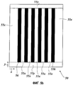
фиг.5 - вид сверху примера выполнения многослойного элемента, образованного в виде пленочного элемента с одномерной рельефной структурой, согласно изобретению;5 is a top view of an exemplary embodiment of a multilayer element formed in the form of a film element with a one-dimensional relief structure, according to the invention;
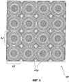
фиг.6 - вид сверху многослойного элемента, выполненного в виде пленочного элемента с двухмерной рельефной структурой, согласно изобретению;6 is a top view of a multilayer element made in the form of a film element with a two-dimensional relief structure, according to the invention;
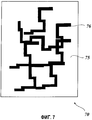
фиг.7 - вид сверху многослойного элемента, выполненного в виде пленочного элемента с электропроводящими линиями, согласно изобретению.7 is a top view of a multilayer element made in the form of a film element with electrically conductive lines, according to the invention.
Описание предпочтительных вариантов выполнения изобретенияDescription of preferred embodiments of the invention
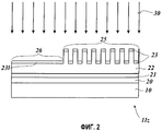
На фиг.1 показан многослойный элемент, образованный в виде элемента из пленки, далее называемый пленочным элементом 11. Пленочный элемент 11 содержит пленку-носитель 10, отделяемый слой 20, слой 21 защитного лака, реплицируемый лаковый слой 22 с рельефными структурами 25 и 26, расположенными на рельефных структурах покрытиями 23l, 23n и слоем 24 клея. Рельефная структура 26 образована в виде плоской рельефной структуры. Рельефная структура 25 представляет собой структуру с высоким значением отношения ширины к глубине, таким образом, эта рельефная структура имеет многократно более высокую эффективную поверхность, чем обычная рельефная структура, например сформированная для получения оптических эффектов в защитных элементах. Рельефная структура 25 образована в форме меандра с перпендикулярными к поверхности плоской рельефной структуры боковыми гранями. В представленном примере выполнения он проходит в одном направлении координат. Таким образом, нанесенное по поверхности покрытие 23n расположено лишь на параллельных поверхности плоской рельефной структуры 26 участках рельефной структуры 25, т.е. речь идет о прерванном в одном направлении координат покрытии. Такая рельефная структура, которая образована с прерыванием в одном направлении координат, в последующем обозначается как одномерная рельефная структура. Как показано на фиг.1, прерывание выполнено сплошным. Напротив, расположенное на плоской рельефной структуре 26 покрытие 23l является замкнутым.Figure 1 shows a multilayer element formed in the form of an element of film, hereinafter referred to as film element 11. The film element 11 comprises a
В представленном примере выполнения с помощью выбора материала и образования рельефной структуры можно получить различные эффекты. Если, например, покрытия 23l, 23n образованы в виде слоев металла, то покрытие 23n является непроводящим металлическим слоем, так как он прерван на вертикальных боковых гранях рельефной структуры. Напротив, нанесенный на плоскую рельефную структуру 26 металлический слой является электропроводящим, так как он не прерывается. Покрытие 23n может быть образовано путем набрызгивания, т.е. с помощью такого способа нанесения покрытия, при котором частицы попадают на рельефную структуру примерно в одинаковом направлении. Поэтому на расположенные параллельно направлению нанесения покрытия вертикальные боковые грани не попадает или попадает незначительное количество частиц, так что там покрытие прервано или образовано с заметно более высоким сопротивлением на единицу поверхности, которое, например, по меньшей мере, в 10 раз выше, предпочтительно в 1000 раз выше, чем сопротивление на единицу поверхности проводящего покрытия 23l вне вертикальных боковых граней.In the illustrated embodiment, various effects can be obtained by selecting a material and forming a relief structure. If, for example, coatings 23l, 23n are formed as metal layers, then coating 23n is a non-conductive metal layer, since it is interrupted at the vertical side faces of the relief structure. On the contrary, a metal layer deposited on a
Такой способ нанесения покрытия отличается тем, что покрытие наносится с постоянной плотностью по поверхности в отношении плоскости, определяемой координатами x и y, причем предпочтительно направление нанесения покрытия может быть ориентировано параллельно вертикальным или почти вертикальным относительно плоскости боковым стенкам рельефной структуры.This method of coating is characterized in that the coating is applied with a constant density over the surface with respect to the plane defined by the x and y coordinates, and preferably the coating direction can be oriented parallel to the side walls of the relief structure that are vertical or almost vertical relative to the plane.
Значительную долю описанного эффекта образования толщины покрытия в зависимости от угла наклона боковых граней имеет высокое значение отношения глубины к ширине рельефной структуры 25, которое предпочтительно составляет >2. Во-первых, благодаря высокому значению отношения глубины к ширине образованы крутые боковые грани, во-вторых, благодаря этому затрудняется случайное осаждение частиц, которые отклоняются от установленного направления нанесения покрытия.A significant proportion of the described effect of the formation of coating thickness depending on the angle of inclination of the side faces has a high value of the ratio of depth to width of the
Другим влияющим фактором является толщина покрытия, которое образовано на плоской рельефной структуре 26. Как показали опыты, описанный выше эффект вступает в действие для толщин <500 нм.Another influencing factor is the thickness of the coating, which is formed on a
Предпочтительно толщина электропроводящего покрытия, которое образовано на рельефной структуре, может быть <50 нм, чтобы получить в рельефной структуре 26 вертикальные или почти вертикальные боковые грани, на которых, по меньшей мере, на отдельных участках не образовано никакого электропроводящего покрытия.Preferably, the thickness of the electrically conductive coating that is formed on the embossed structure may be <50 nm to obtain vertical or near-vertical side faces in the embossed
Может быть предусмотрено выполнить такой слой прозрачным, например толщиной около 10 нм. Таким способом можно сформировать проводящие линии, которые визуально не перекрывают расположенные под ними структуры, например индицирующие LCD-элементы.It may be envisaged to make such a layer transparent, for example, about 10 nm thick. In this way, conductive lines can be formed that do not visually overlap the structures below them, for example, LCD-indicating elements.
В пленочном элементе 11 речь идет о пленке для тиснения, в частности о пленке для горячего тиснения. Однако можно образовать пленочный элемент 11 в виде клейкой пленки или в качестве носителя для переключающей схемы, в частности полимерной переключающей схемы.The film element 11 refers to a film for embossing, in particular a film for hot stamping. However, it is possible to form the film element 11 in the form of an adhesive film or as a carrier for a switching circuit, in particular a polymer switching circuit.
Несущий слой 10 состоит, например, из PET-пленки (полиэтилентерефталатной пленки) или POPP-пленки (полипропиленовой пленки) толщиной от 10 мкм до 50 мкм, предпочтительно толщиной 19-23 мкм. На пленку-носитель затем с помощью валика с сетчатой поверхностью для глубокой печати наносятся отделяемый слой 20 и слой 21 защитного лака. Отделяемый слой и защитный лаковый слой 20 и 21 имеют при этом толщину предпочтительно от 0,2 до 1,2 мкм. От этих слоев можно также отказаться.The
Затем наносится реплицируемый лаковый слой 22.Then, a replicated
Реплицируемый лаковый слой 22 состоит преимущественно из сшиваемого под излучением реплицируемого лака. Предпочтительно способ репликации под воздействием ультрафиолетового излучения применяется для формирования рельефных структур 25 и 26 в реплицируемом лаковом слое 22. В качестве реплицируемого лака при этом используется лак, отверждаемый с помощью ультрафиолетовых лучей. Введение рельефных структур 25 и 26 в реплицируемый, сшиваемый под воздействием ультрафиолетовых лучей лаковый слой осуществляется при этом, например, путем УФ-облучения при формировании рельефной структуры в еще мягком или жидком слое лака или путем частичного облучения и отверждения сшиваемого при УФ-облучении слоя лака. Вместо сшиваемого при УФ-облучении лака можно использовать также иной сшиваемый под воздействием излучения лак.The replicated
Возможно также, чтобы реплицируемый лаковый слой 22 состоял из прозрачного термопластичного синтетического материала. В реплицируемом лаковом слое 22 затем с помощью инструмента для тиснения выдавливается рельефная структура или выдавливается несколько рельефных структур, например рельефные структуры 25 и 26.It is also possible for the replicated
Толщина, которую выбирают для реплицируемого лакового слоя 22, определяется выбранной для рельефной структуры 25 глубиной профиля. Необходимо, чтобы реплицируемый лаковый слой 22 имел достаточную толщину, чтобы обеспечить формирование рельефных структур 25 и 26. Предпочтительно реплицируемый лаковый слой имеет толщину от 0,1 до 10 мкм.The thickness selected for the replicated
Например, реплицируемый лаковый слой 22 наносится на защитный лаковый слой 21 перед сушкой с весом на единицу поверхности 2,2 г/м2 с помощью линейного растрового валика для глубокой печати на всю поверхность. В качестве реплицируемого лака выбирают при этом лак следующего состава:For example, a replicated
Затем реплицируемый лаковый слой 22 подвергается сушке в сушильном канале при температуре 100-120°С.Then, the replicated
После этого в реплицируемом лаковом слое 22 при температуре около 130°С выдавливаются рельефные структуры 25 и 26, например, с помощью матрицы, состоящей из никеля. Для тиснения рельефных структур 25 и 26 матрицу предпочтительно подвергают электронагреву. Перед отделением матрицы от реплицируемого лакового слоя после тиснения матрицу этом снова охладить. После тиснения рельефных структур 25 и 26 реплицируемый лак реплицируемого слоя 22 отверждается путем сшивания или иным способом.After that, in the replicated
Затем возможно вносить рельефные структуры 25 и 26 в реплицируемый лаковый слой 22 путем абляции (вымывания).Then it is possible to introduce the
Рельефные структуры 25 и 26 содержат структуры, которые покрыты покрытиями 23l, 23n известным способом напыления.The
Как видно из фиг.2, направление нанесения покрытия при осаждении покрытий 23l, 23n ориентировано перпендикулярно к поверхности плоской рельефной структуры 16. Направление нанесения покрытия показано стрелкой 30. При этом устройство для нанесения покрытия работает таким образом, что материал на рельефных структурах 25 и 26 осаждается с постоянной плотностью по поверхности, так что в результате плотность по поверхности покрытий 23l, 23n на рельефных структурах 25 и 26 одинакова и постоянна. Таким образом, не требуется никаких дополнительных операций, чтобы, например, получить различную проводимость покрытий 23l, 23n и/или чтобы получить определенную геометрию покрытий 23l, 23n. При этом особенно предпочтительно, чтобы структурирование покрытий 23l, 23n было выполнено с точной пригонкой в процессе одной технологической операции и чтобы вследствие микроструктурирования рельефных структур достичь высокого разрешения, что необходимо, например, для изготовления переключающих схем.As can be seen from figure 2, the coating direction during deposition of coatings 23l, 23n is oriented perpendicular to the surface of the flat relief structure 16. The coating direction is shown by
Затем на покрытия 23l, 23n наносится слой 24 клея. Слой 24 клея предпочтительно представляет слой из термически активируемого клея. В зависимости от применения защитного элемента 11 возможно отказаться от слоя 24 клея.An
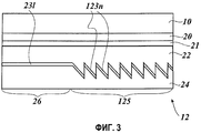
На фиг.3 показан второй вариант выполнения многослойного элемента в форме пленочного элемента 12 с одномерной рельефной структурой, который отличается от описанного выше примера выполнения лишь формой рельефной структуры. Пленочный элемент 12 вместо имеющей форму меандра рельефной структуры 25 (фиг.1) выполнен с пилообразной рельефной структурой 125. Рельефная структура 125 имеет расположенную перпендикулярно поверхности плоской рельефной структуры 26 первую боковую грань и расположенную под углом относительно первой боковой грани вторую боковую грань. Таким образом, покрытие 23n расположено только на вторых боковых гранях, т.е. покрытие прерывается.Figure 3 shows a second embodiment of a multilayer element in the form of a
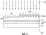
На фиг.4 показано нанесение на рельефные структуры 125 и 26 покрытий 123n и 23l. Как описано выше для фиг.2, покрытия 123n и 23l наносятся известным образом, например путем напыления на рельефные структуры 125 или 26. Как показано на фиг.4, на расположенных под углом вторых боковых гранях рельефной структуры 125 покрытие 123n выполнено меньшей толщины, чем на грани, расположенной перпендикулярно к направлению нанесения рельефной структуры 26. Так как покрытие 123n прервано перпендикулярными первыми боковыми гранями рельефной структуры 125, которая не покрыта материалом, нанесенный таким образом слой металла является неэлектропроводящим.Figure 4 shows the deposition of
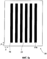
На фиг.5а схематически показан вид сверху многослойного элемента, выполненного в виде пленочного элемента 50 с одномерной рельефной структурой, которая в представленном примере выполнения покрыта металлом. Сформирована неэлектропроводящая область 55 с одномерной рельефной структурой с высоким отношением глубины к ширине (фиг.1 и 3) (поз.25 или 125), в которую включена показанная черным цветом проводящая плоская область 56. Речь идет об электропроводящих линиях, которые соединяют друг с другом электрические конструктивные элементы (не показаны).On figa schematically shows a top view of a multilayer element made in the form of a
Хотя неэлектропроводящая область 55 прервана не имеющими покрытия вертикальными боковыми гранями лишь в направлении х координат и на участках 55k, в которых она в направлении y примыкает к электропроводящей области 56, является локально электрически короткозамкнутой, она имеет в целом электрическую проводимость, которая на порядок меньше, чем электрическая проводимость области 56.Although the
На фиг.5b показано, как локального короткого замыкания можно избежать с помощью проводящих областей 56. Для этого область 55 подразделяется на области 55x и области 55y, рельефная структура которых изменяется в направлении х или в направлении у. Такая конструкция может быть предусмотрена, если электропроводящие области 56 расположены не параллельно друг другу или образованы в виде кривых.Fig. 5b shows how a local short circuit can be avoided by using
Можно области 56 утолщить путем нанесения гальванического покрытия. Так как области 55, 55x и 55y выполнены неэлектропроводящими, то при нанесении гальванического покрытия не осаждается никакого металла, т.е. не требуется никаких дополнительных операций, чтобы утолщить с помощью нанесения гальванического покрытия только проводящие области 56. Таким образом, проводящие плоские области 56 выполнены с меньшим удельным сопротивлением, чем перед нанесением гальванического покрытия. Поэтому можно отказаться от преобразования области 55 (фиг.5а) в различно ориентированные области 55х и 55у (фиг.5b), так как электрическая проводимость области 56 значительно больше, чем электрическая проводимость области 55.
Представленные на фиг.5а и 5b области 56 могут быть выполнены прозрачными, например, если нанесен очень тонкий слой металла порядка 10 нм, изменяемый в зависимости от вида металла.The
На фиг.6 показан вид сверху многослойного элемента, выполненного в виде пленочного элемента 60 с растровыми элементами 62, которые имеют рельефные структуры 65 с большим отношением глубины к ширине и вертикальными боковыми гранями, которые образуют замкнутые профилированные кривые 65p. В описываемом варианте выполнения профилированные кривые образованы в виде окружностей и ромбов. Пленочный элемент 60 покрыт слоем металла (не показан), который является неэлектропроводящим из-за рельефных структур 65. Речь идет при этом о двухмерной рельефной структуре, в которой исключено короткое замыкание через электропроводящие области. Рельефные структуры 65 образованы из расположенных концентрически окружностей, которые вписаны в квадратные растровые элементы 62. Таким образом, сегменты окружности угловой области с сегментами окружности расположенных по соседству с этой угловой областью трех других растровых элементов 62 образуют ромбические профилированные кривые.Figure 6 shows a top view of a multilayer element made in the form of a
Можно предусмотреть, чтобы растровые элементы 62 были выполнены одинаковой формы и одинаковой величины, т.е. в виде равносторонних треугольников, квадратов или шестиугольников. Можно также образовать растровые элементы различной формы, т.е. заполнить поверхность пленочного элемента 60 растровыми элементами различной формы и величины. Важно лишь, чтобы вертикальные боковые грани рельефной структуры 65 образовывали замкнутые кривые.It can be provided that the
На фиг.7 представлен многослойный, покрытый металлом элемент, образованный из пленочного элемента 70 со структурированным проводником 76, который окружен областями 75, выполненными с рельефными структурами с большим отношением глубины к ширине. Рельефные структуры могут быть выполнены в виде одномерных рельефных структур (фиг.5) или двухмерных рельефных структур (фиг.6) с большим отношением глубины к ширине. Предпочтительной является двухмерная рельефная структура и отношение глубины к ширине >2.7 shows a multilayer, metal-coated element formed of a
Пленочный элемент 70 может быть образован в виде части микроэлектронной переключающей схемы, например в виде части, выполненной в виде пленочной системы полимерной переключающей схемы. При этом переключающая схема может быть выполнена прозрачной, как описано выше (фиг.5).The
Можно предусмотреть, чтобы один или несколько участков структурированного проводника 76 имели рельефную структуру с высоким отношением глубины к ширине, чтобы на таком участке электрическая проводимость проводника 76 была более низкой. Таким образом, в проводнике 76 могут быть образованы электрические сопротивления.It can be envisaged that one or more sections of the structured
Claims (23)
первая рельефная структура (25, 125, 65) является структурой с большим отношением глубины к ширине отдельных структурных элементов, в частности с отношением глубины к ширине >2, и содержит, по меньшей мере, одну вертикальную или почти вертикальную боковую грань, проходящую по всей глубине или почти всей глубине рельефной структуры, при этом на боковой грани первой рельефной структуры (25, 125, 65) сформированы участки, на которые не осаждено электропроводящее покрытие (231, 23n, 123n), нанесенное на первую рельефную структуру, или осаждено слоем очень малой толщины, так что электрическая проводимость покрытия (231, 23n, 123n) в области боковой грани является значительно более низкой.1. A multilayer element (11, 12) with a replicated varnish layer (22), in which the first relief structure (25, 125, 65) is formed in the replicated varnish layer (22) in the plane defined by the x and y coordinate axes, in the first region a multilayer element, and a conductive coating (231, 23n, 123n) with a constant density on the surface is applied to the replicated varnish layer (22) in the first region of the multilayer element (11, 12) and in the adjacent second region of the multilayer element (11, 12), characterized the fact that
the first relief structure (25, 125, 65) is a structure with a large ratio of depth to width of individual structural elements, in particular with a ratio of depth to width> 2, and contains at least one vertical or almost vertical side face that runs along the entire the depth or almost the entire depth of the relief structure, while on the lateral edge of the first relief structure (25, 125, 65), areas are formed on which the electrically conductive coating (231, 23n, 123n) is not deposited, applied to the first relief structure, or is very deposited by a layer few thickness so that the electrical conductivity of the coating (231, 23n, 123n) in the area of the side faces is considerably lower.
Applications Claiming Priority (2)
| Application Number | Priority Date | Filing Date | Title |
|---|---|---|---|
| DE102004042111.0 | 2004-08-30 | ||
| DE102004042111A DE102004042111A1 (en) | 2004-08-30 | 2004-08-30 | Multi-layered body with different microstructured areas with electrically conductive coating |
Publications (2)
| Publication Number | Publication Date |
|---|---|
| RU2007111712A RU2007111712A (en) | 2008-10-10 |
| RU2379861C2 true RU2379861C2 (en) | 2010-01-20 |
Family
ID=35789315
Family Applications (1)
| Application Number | Title | Priority Date | Filing Date |
|---|---|---|---|
| RU2007111712/09A RU2379861C2 (en) | 2004-08-30 | 2005-08-24 | Multi-layer element with zones of varying microstructure incorporating conducting coating |
Country Status (13)
| Country | Link |
|---|---|
| US (1) | US20080095986A1 (en) |
| EP (1) | EP1785016B1 (en) |
| JP (1) | JP4852547B2 (en) |
| KR (1) | KR101184096B1 (en) |
| CN (1) | CN100576974C (en) |
| AT (1) | ATE432607T1 (en) |
| DE (2) | DE102004042111A1 (en) |
| ES (1) | ES2327943T3 (en) |
| MX (1) | MX2007002118A (en) |
| PL (1) | PL1785016T3 (en) |
| RU (1) | RU2379861C2 (en) |
| TW (1) | TW200619434A (en) |
| WO (1) | WO2006024441A2 (en) |
Families Citing this family (12)
| Publication number | Priority date | Publication date | Assignee | Title |
|---|---|---|---|---|
| DE102006034095B4 (en) * | 2006-07-20 | 2009-05-28 | Leonhard Kurz Gmbh & Co. Kg | Solar cell based on polymer |
| DE102006050047A1 (en) | 2006-10-24 | 2008-04-30 | Giesecke & Devrient Gmbh | Transparent security element for security papers, data carrier, particularly valuable documents such as bank note, identification card and for falsification of goods, has transparent substrate and marking layer applied on substrate |
| DE102007005416B4 (en) * | 2007-01-30 | 2016-03-31 | Leonhard Kurz Gmbh & Co. Kg | Embossing foil and thus formed safety sticker |
| DE102007005088B4 (en) * | 2007-02-01 | 2011-08-25 | Leonhard Kurz GmbH & Co. KG, 90763 | Solar cell and process for its production |
| DE102007046679B4 (en) | 2007-09-27 | 2012-10-31 | Polyic Gmbh & Co. Kg | RFID transponder |
| DE102008017652A1 (en) * | 2008-04-04 | 2009-10-08 | Leonhard Kurz Stiftung & Co. Kg | Security element and method for producing a security element |
| JP5568973B2 (en) * | 2009-12-11 | 2014-08-13 | 凸版印刷株式会社 | Anti-counterfeit medium, anti-counterfeit label and article |
| KR102209571B1 (en) * | 2014-12-31 | 2021-02-01 | 한국조폐공사 | Hologram with polarization image |
| FR3068563B1 (en) * | 2017-07-03 | 2019-10-04 | Valeo Iluminacion | ELECTRICAL CIRCUIT ON A LIGHT VEHICLE DEVICE |
| CN111103214B (en) * | 2019-04-19 | 2022-07-29 | 宁德时代新能源科技股份有限公司 | Coating surface density detection device and method |
| CN111103213B (en) * | 2019-04-19 | 2022-07-29 | 宁德时代新能源科技股份有限公司 | Coating surface density detection device and method |
| US20220241781A1 (en) * | 2019-05-10 | 2022-08-04 | Leonhard Kurz Stiftung & Co. Kg | Microfluidic array, method of manufacture, measuring system comprising the microfluidic array, and use |
Family Cites Families (25)
| Publication number | Priority date | Publication date | Assignee | Title |
|---|---|---|---|---|
| FR1013410A (en) * | 1950-03-02 | 1952-07-29 | Circle for cheese making | |
| DE3650027T2 (en) * | 1985-05-07 | 1995-01-26 | Dainippon Printing Co Ltd | Item with transparent hologram. |
| JPH0614579B2 (en) * | 1985-08-27 | 1994-02-23 | 三菱電線工業株式会社 | Metal core substrate and manufacturing method thereof |
| JPS62134295A (en) * | 1985-12-06 | 1987-06-17 | 松下電器産業株式会社 | Integrated circuit card |
| JP3159558B2 (en) * | 1993-02-25 | 2001-04-23 | 関西ペイント株式会社 | Radio wave antireflective body and radio wave antireflection method |
| FR2716748B1 (en) * | 1994-02-25 | 1996-06-07 | France Telecom | Upholstery or filling process by gas phase deposition of a relief structure and application of this process for the manufacture of semiconductor elements. |
| JPH07312322A (en) * | 1994-03-24 | 1995-11-28 | Meidensha Corp | Winding method of stationary induction electric apparatus |
| CH690067A5 (en) * | 1995-08-10 | 2000-04-14 | Ovd Kinegram Ag | A process for preparing teilmetallisierter lattice structures. |
| GB9623185D0 (en) * | 1996-11-09 | 1997-01-08 | Epigem Limited | Improved micro relief element and preparation thereof |
| JPH11186773A (en) * | 1997-12-25 | 1999-07-09 | Sharp Corp | Electromagnetic wave shielding cabinet, its manufacture and metal mold equipment |
| DE19822075C2 (en) * | 1998-05-16 | 2002-03-21 | Enthone Gmbh | Process for the metallic coating of substrates |
| JP2000098132A (en) * | 1998-09-17 | 2000-04-07 | Toppan Printing Co Ltd | Polarizing beam splitter having electromagnetic wave shielding effect |
| JP2000113151A (en) * | 1998-10-01 | 2000-04-21 | Tomoegawa Paper Co Ltd | Label-type ic card |
| JP2000124663A (en) * | 1998-10-16 | 2000-04-28 | Toyobo Co Ltd | Electromagnetic wave shielding film |
| JP2001256457A (en) * | 2000-03-13 | 2001-09-21 | Toshiba Corp | Semiconductor device, its manufacture and ic card communication system |
| US20020041009A1 (en) * | 2000-07-05 | 2002-04-11 | Matsushita Electric Industrial Co., Ltd | Transmission line assembly chip and a manufacturing method thereof in a multi-chip module |
| JP2002356542A (en) * | 2001-05-31 | 2002-12-13 | Canon Inc | Polyhydroxyalkanoate-containing card |
| WO2003082598A2 (en) * | 2002-04-03 | 2003-10-09 | De La Rue International Limited | Optically variable security device |
| JP4019770B2 (en) * | 2002-04-05 | 2007-12-12 | ソニー株式会社 | Satellite broadcast receiving tuner unit, satellite broadcast receiving front end unit, and satellite broadcast receiving apparatus |
| EP1525102B1 (en) * | 2002-07-18 | 2012-09-26 | Giesecke & Devrient GmbH | Security document |
| JP2004077954A (en) * | 2002-08-21 | 2004-03-11 | Dainippon Printing Co Ltd | Medium and method for confirming authenticity |
| US7001658B2 (en) * | 2003-04-28 | 2006-02-21 | Eastman Kodak Company | Heat selective electrically conductive polymer sheet |
| DE10333255B3 (en) * | 2003-07-21 | 2005-01-13 | Leonhard Kurz Gmbh & Co. Kg | Applying high-resolution pattern to substrate, for hot-stamped laminated film or transfer films, by defining fine structuring by orientation direction and profile shape of microscopic surface structure |
| WO2005017570A2 (en) * | 2003-08-06 | 2005-02-24 | University Of Pittsburgh | Surface plasmon-enhanced nano-optic devices and methods of making same |
| JP4747627B2 (en) * | 2004-07-23 | 2011-08-17 | 日立化成工業株式会社 | Diffraction type condensing film and surface light source device using the same |
-
2004
- 2004-08-30 DE DE102004042111A patent/DE102004042111A1/en not_active Ceased
-
2005
- 2005-08-24 DE DE502005007362T patent/DE502005007362D1/en active Active
- 2005-08-24 KR KR1020077007397A patent/KR101184096B1/en active IP Right Grant
- 2005-08-24 PL PL05776119T patent/PL1785016T3/en unknown
- 2005-08-24 AT AT05776119T patent/ATE432607T1/en active
- 2005-08-24 JP JP2007528740A patent/JP4852547B2/en active Active
- 2005-08-24 US US11/661,484 patent/US20080095986A1/en not_active Abandoned
- 2005-08-24 CN CN200580028846A patent/CN100576974C/en active Active
- 2005-08-24 MX MX2007002118A patent/MX2007002118A/en active IP Right Grant
- 2005-08-24 WO PCT/EP2005/009137 patent/WO2006024441A2/en active Application Filing
- 2005-08-24 RU RU2007111712/09A patent/RU2379861C2/en not_active IP Right Cessation
- 2005-08-24 ES ES05776119T patent/ES2327943T3/en active Active
- 2005-08-24 EP EP05776119A patent/EP1785016B1/en active Active
- 2005-08-26 TW TW094129266A patent/TW200619434A/en not_active IP Right Cessation
Also Published As
| Publication number | Publication date |
|---|---|
| CN101010995A (en) | 2007-08-01 |
| TW200619434A (en) | 2006-06-16 |
| EP1785016A2 (en) | 2007-05-16 |
| WO2006024441A2 (en) | 2006-03-09 |
| WO2006024441A3 (en) | 2006-05-11 |
| US20080095986A1 (en) | 2008-04-24 |
| DE502005007362D1 (en) | 2009-07-09 |
| PL1785016T3 (en) | 2009-10-30 |
| JP2008511846A (en) | 2008-04-17 |
| EP1785016B1 (en) | 2009-05-27 |
| KR20070062535A (en) | 2007-06-15 |
| TWI361229B (en) | 2012-04-01 |
| ATE432607T1 (en) | 2009-06-15 |
| JP4852547B2 (en) | 2012-01-11 |
| CN100576974C (en) | 2009-12-30 |
| MX2007002118A (en) | 2007-10-02 |
| ES2327943T3 (en) | 2009-11-05 |
| RU2007111712A (en) | 2008-10-10 |
| DE102004042111A1 (en) | 2006-03-09 |
| KR101184096B1 (en) | 2012-09-18 |
Similar Documents
| Publication | Publication Date | Title |
|---|---|---|
| RU2379861C2 (en) | Multi-layer element with zones of varying microstructure incorporating conducting coating | |
| KR101306403B1 (en) | Multi-layer body and method for producing the same | |
| RU2384417C2 (en) | Optically variable element with electrically active layer | |
| RU2377134C2 (en) | Counterfeit-protected symbol with variable-colour effect | |
| AU2014266990B2 (en) | Security documents and methods of manufacture thereof | |
| CN1296728A (en) | Thin film transferable electric components | |
| RU2337832C2 (en) | Method for obtaining surface image with high resolution | |
| KR101196591B1 (en) | Film comprising organic semiconductors | |
| US20060164249A1 (en) | Security element for radio frequency identification | |
| RU2517506C2 (en) | Device electronic and/or optical unit and method of its configuration | |
| WO2012038490A1 (en) | Multiple information carrier | |
| RU2566928C2 (en) | Microrelief structure, | |
| CN114475043B (en) | Optical anti-counterfeiting element, manufacturing method thereof and anti-counterfeiting product | |
| KR20170040070A (en) | A method of manufacturing metal stamps | |
| RU2310241C2 (en) | Method for manufacturing holographic labels |
Legal Events
| Date | Code | Title | Description |
|---|---|---|---|
| MM4A | The patent is invalid due to non-payment of fees |
Effective date: 20200825 |