RU2255343C2 - Group delay time measuring unit - Google Patents
Group delay time measuring unit Download PDFInfo
- Publication number
- RU2255343C2 RU2255343C2 RU2003137022/28A RU2003137022A RU2255343C2 RU 2255343 C2 RU2255343 C2 RU 2255343C2 RU 2003137022/28 A RU2003137022/28 A RU 2003137022/28A RU 2003137022 A RU2003137022 A RU 2003137022A RU 2255343 C2 RU2255343 C2 RU 2255343C2
- Authority
- RU
- Russia
- Prior art keywords
- input
- output
- register
- measuring unit
- inputs
- Prior art date
Links
Images

Abstract
Description
Изобретение относится к области радиоизмерений и может быть использовано для измерения временного сдвига, возникающего в реальных четырехполюсниках, например в усилителях аудиосигналов, между выходным и входным сигналами, носящими как случайный характер, так и детерминированный моногармонический.The invention relates to the field of radio measurements and can be used to measure the time shift occurring in real four-port networks, for example, in audio signal amplifiers, between output and input signals that are both random and deterministic monoharmonic.
В качестве прототипа, как наиболее близкий по технической сущности, выбран классический измеритель (фазометр), применяемый для оценки относительных временных сдвигов в усилительных устройствах и содержащий два формирователя импульсов, блок выделения временного интервала и блок измерения временных сдвигов, выход которого является выходом измерителя, входом запаздывающего сигнала является вход первого формирователя, входом опережающего сигнала является вход второго формирователя, выходы первого и второго формирователей подключены соответственно к первому и второму входам блока выделения временного интервала, выходы которого подключены к входам блока измерения временных сдвигов [Электрические измерения / Под ред. А.В.Фремке и Е.М.Душина. - 5-е изд., перераб. и доп.- Л.: Энергия, 1980, стр.243-244, рис. 6.19 а, б].As a prototype, as the closest in technical essence, a classic meter (phase meter) is selected, used to estimate relative time shifts in amplifying devices and containing two pulse shapers, a time interval allocation unit and a time shift measuring unit, the output of which is the output of the meter, input the delayed signal is the input of the first driver, the input of the leading signal is the input of the second driver, the outputs of the first and second drivers are connected with responsibly to the first and second inputs of the block allocation time slot, which outputs are connected to inputs of the measurement unit time shifts [Electrical measurements / Ed. A.V. Fremke and E.M. Dushina. - 5th ed., Revised. and additional - L .: Energy, 1980, pp. 243-244, fig. 6.19 a, b].
В прототипе реализован широко известный метод измерения фазовых сдвигов и группового времени запаздывания, основанный на выделении моментов пересечения сигналами нулевой линии и измерении временного сдвига между указанными моментами - опорными временными метками. К существенному недостатку как самого метода, так и устройств, его реализующих, следует отнести погрешность, обусловленную не совсем корректным определением положения временных меток как одноименных точек входного и выходного сигналов, между которыми затем измеряют временное запаздывание. Так, при изменении положения нулевой линии выходного сигнала формируемые вышеуказанным путем временные метки также будут смещаться, что приведет к появлению ошибки в измерениях временного сдвига, а следовательно, и группового времени запаздывания. Причем смещение нулевой линии возможно не только в усилителях постоянного тока или в видеоусилителях, но и в усилителях переменного тока, например в усилителях аудиосигналов, так как к подобному эффекту приводит и нелинейное преобразование с последующим центрированием (то есть то, что происходит в реальных усилителях). При нелинейном преобразовании в спектре выходного сигнала появляется постоянная составляющая, после удаления которой результирующий процесс на нагрузке смещается вдоль оси ординат таким образом, чтобы площади под разнополярными полуволнами оказались равными - это приводит к смещению во времени моментов формирования опорных временных меток. В результате с увеличением нелинейных искажений увеличивается и ошибка измерения группового времени запаздывания. Учитывая, что искажения, как правило, растут с увеличением амплитуды входного сигнала, то оценка искомого времени запаздывания также будет зависеть от амплитуды входного сигнала, в то время как истинное значение времени группового запаздывания не меняется.The prototype implements a well-known method for measuring phase shifts and group delay times, based on the allocation of the moments of crossing the zero line signals and measuring the time shift between the indicated moments - reference time stamps. An essential drawback of both the method itself and the devices that implement it is the error due to the not quite correct determination of the position of the time marks as the same points of the input and output signals, between which the time delay is then measured. So, when the position of the output signal's zero line changes, the time marks generated by the above path will also shift, which will lead to an error in the measurements of the time shift, and hence the group delay time. Moreover, the zero line offset is possible not only in DC amplifiers or in video amplifiers, but also in AC amplifiers, for example, audio signal amplifiers, since a nonlinear transformation with subsequent centering leads to a similar effect (that is, what happens in real amplifiers) . During nonlinear transformation, a constant component appears in the spectrum of the output signal, after which the resulting process on the load shifts along the ordinate so that the areas under the bipolar half-waves are equal - this leads to a shift in time of the formation of the reference time stamps. As a result, with an increase in the nonlinear distortion, the error in measuring the group delay time also increases. Considering that distortions, as a rule, increase with the amplitude of the input signal, the estimate of the sought delay time will also depend on the amplitude of the input signal, while the true value of the group delay time does not change.
Технический результат, достигаемый при использовании настоящего изобретения, состоит главным образом в повышении точности оценки группового времени запаздывания при смещении нулевой линии и нелинейных искажениях.The technical result achieved by using the present invention consists mainly in improving the accuracy of estimating group delay time with zero line offset and non-linear distortions.
Технический результат достигается тем, что в измеритель группового времени запаздывания, включающий в себя блок измерения временных сдвигов, выход которого является выходом измерителя, согласно изобретению введены два блока выделения экстремума, вход первого из них является входом запаздывающего сигнала, вход второго блока выделения экстремума является входом опережающего сигнала, выходы первого и второго блоков выделения экстремума подключены соответственно к первому и второму входам блока измерения временных сдвигов.The technical result is achieved by the fact that in the group delay time meter, which includes a time shift measuring unit, the output of which is the output of the meter, according to the invention two extremum extraction units are introduced, the input of the first one is the input of the delayed signal, the input of the second extremum extraction unit is the input leading signal, the outputs of the first and second extremum extraction units are connected respectively to the first and second inputs of the time shift measurement unit.
Для достижения технического результата блок выделения экстремума содержит аналого-цифровой преобразователь, три регистра, два компаратора двоичных кодов, элемент И и три элемента задержки, информационный вход аналого-цифрового преобразователя служит входом блока выделения экстремума, выходом которого служит выход элемента И, выход аналого-цифрового преобразователя соединен с информационным входом первого регистра, выход которого соединен с информационным входом второго регистра, выход которого соединен с информационным входом третьего регистра, к выходу первого регистра подключен первый вход первого компаратора, второй вход которого подключен к выходу второго регистра, первый вход второго компаратора подключен к выходу третьего регистра, а второй вход второго компаратора объединен со вторым входом первого компаратора, выходы первого и второго компараторов подключены соответственно к первому и второму входам элемента И, третий вход которого соединен с выходом первого элемента задержки, вход которого подключен к тактовому входу блока, тактовые входы аналого-цифрового преобразователя и третьего регистра объединены и также подключены к тактовому входу блока, тактовый вход первого регистра соединен с выходом второго элемента задержки, вход которого соединен с выходом третьего элемента задержки, вход которого подключен к тактовому входу блока, тактовый вход второго регистра соединен с выходом третьего элемента задержки.To achieve a technical result, the extremum extraction unit contains an analog-to-digital converter, three registers, two binary code comparators, an And element, and three delay elements, the information input of an analog-to-digital converter serves as the input of an extremum extraction unit, the output of which is the output of the And element, the output of the digital converter is connected to the information input of the first register, the output of which is connected to the information input of the second register, the output of which is connected to the information input of the of the first register, the first input of the first comparator is connected, the second input of which is connected to the output of the second register, the first input of the second comparator is connected to the output of the third register, and the second input of the second comparator is combined with the second input of the first comparator, the outputs of the first and second comparators are connected respectively, to the first and second inputs of the And element, the third input of which is connected to the output of the first delay element, the input of which is connected to the clock input of the block, the analog-to-digital clock inputs the new converter and the third register are combined and also connected to the clock input of the block, the clock input of the first register is connected to the output of the second delay element, the input of which is connected to the output of the third delay element, the input of which is connected to the clock input of the block, the clock input of the second register is connected to the output of the third delay element.
Сущность изобретения поясняется графическим материалом. На фиг.1 представлена функциональная схема измерителя группового времени запаздывания с подключенным тестируемым усилителем. На фиг.2 показаны временные диаграммы, поясняющие принцип измерений. На фиг.3 представлена функциональная схема блока выделения экстремума.The invention is illustrated graphic material. Figure 1 presents the functional diagram of the group delay meter with a connected tested amplifier. Figure 2 shows the timing diagrams explaining the principle of measurement. Figure 3 presents the functional diagram of the block selection of the extremum.
Функциональная схема по фиг.1 содержит два блока 1, 2 выделения экстремума, блок 3 измерения временных сдвигов и тестируемый усилитель 4 с нагрузкой RL. Выход усилителя 4 соединен с входом запаздывающего сигнала y(t) измерителя, которым (входом) служит вход блока 1, выход которого соединен с первым входом блока 3 измерения временных сдвигов, второй вход которого соединен с выходом блока 2, вход которого является входом опережающего сигнала x(t) измерителя и объединен со входом тестируемого усилителя 4, выходом τ* измерителя является выход блока 3.The functional diagram of figure 1 contains two blocks 1, 2 selection of the extremum, block 3 measuring the time shifts and the tested amplifier 4 with a load R L. The output of amplifier 4 is connected to the input of the delayed signal y (t) of the meter, which (input) is the input of block 1, the output of which is connected to the first input of block 3 for measuring time shifts, the second input of which is connected to the output of block 2, whose input is an input of the leading signal x (t) of the meter and combined with the input of the tested amplifier 4, the output τ * of the meter is the output of block 3.
Функциональная схема (фиг.3) блока 1 (2) выделения экстремума содержит аналого-цифровой преобразователь (АЦП) 5, регистры 6, 7, 8, компараторы 9, 10, элемент И 11 и элементы 12, 13, 14 задержки. Информационный вход x(t), y(t) АЦП 5 служит входом блока, выходом которого служит выход элемента И 11, выход АЦП 5 соединен с информационным входом регистра 6, выход которого соединен с информационным входом регистра 7, выход которого соединен с информационным входом регистра 8, к выходу регистра 6 подключен вход А компаратора 9, вход В которого подключен к выходу регистра 7, вход А компаратора 10 подключен к выходу регистра 8, а вход В компаратора 10 объединен со входом В компаратора 9, выходы компараторов 9, 10 подключены соответственно к первому и второму входам элемента И 11, третий вход которого соединен с выходом элемента 14 задержки, вход которого подключен к тактовому входу CLK блока, тактовые входы АЦП 5 и регистра 8 объединены и также подключены к тактовому входу CLK блока, тактовый вход регистра 6 соединен с выходом элемента 12 задержки, вход которого соединен с выходом элемента 13 задержки, вход которого подключен к тактовому входу CLK блока, тактовый вход регистра 7 соединен с выходом элемента 13 задержки. Выход АЦП 5, информационные входы и выходы регистров 6, 7, 8, а также входы компараторов 9, 10 являются многоразрядными и предназначены для работы с параллельными кодами.Functional diagram (figure 3) of block 1 (2) of extremum extraction contains an analog-to-digital converter (ADC) 5,
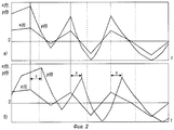
Временные диаграммы (фиг.2) содержат входной x(t) и выходной y(t) сигналы тестируемого усилителя 4 в предположении, что групповое время запаздывания равно нулю (фиг.2а), а усилитель 4 обладает свойствами нелинейного четырехполюсника; входной x(t) и выходной y(t) сигналы тестируемого усилителя 4 в предположении, что групповое время запаздывания отлично от нуля и равно τ (фиг.2б), а усилитель 4 обладает свойствами нелинейного четырехполюсника.Timing diagrams (Fig. 2) contain the input x (t) and output y (t) signals of the tested amplifier 4 under the assumption that the group delay time is zero (Fig. 2a), and the amplifier 4 has the properties of a nonlinear four-terminal network; input x (t) and output y (t) signals of the tested amplifier 4 under the assumption that the group delay time is different from zero and equal to τ (Fig.2b), and amplifier 4 has the properties of a nonlinear four-terminal network.
Принцип действия измерителя (фиг.1) на функциональном уровне достаточно прост и состоит в выделении блоками 1, 2 точек экстремума входного х(t) и выходного y(t) сигналов, а затем измерении в блоке 3 временного сдвига τ между ними. Измерение временных сдвигов между экстремумами позволяет избавиться от погрешностей, вызванных колебаниями (смещениями) нулевой линии и влиянием нелинейных искажений на форму выходного сигнала. Из графиков, приведенных на фиг.2а, видно, что при нелинейном усилении даже при полном отсутствии временного запаздывания точки пересечения нулевой линии входным х(t) и выходным y(t) сигналами расположены в разных местах. Что же касается расположения экстремумов, то они при незначительных нелинейных искажениях не смещаются, также как и при изменении положения нулевой линии. По указанным причинам для измерения группового времени запаздывания или фазовых сдвигов целесообразно выделять точки экстремума и измерять временное расстояние между ними, как это показано для случая моделирования нелинейного усиления случайного процесса на фиг.2б.The principle of operation of the meter (Fig. 1) at the functional level is quite simple and consists in the allocation by blocks 1, 2 of the extremum points of the input x (t) and output y (t) signals, and then measuring the time shift τ between them in block 3. Measurement of time shifts between extrema allows you to get rid of errors caused by vibrations (offsets) of the zero line and the influence of nonlinear distortions on the shape of the output signal. From the graphs shown in figa, it can be seen that with nonlinear amplification, even in the complete absence of time delay, the points of intersection of the zero line with the input x (t) and output y (t) signals are located in different places. As for the location of the extrema, they do not shift with slight nonlinear distortions, as well as when the position of the zero line changes. For these reasons, to measure the group delay time or phase shifts, it is advisable to select the extremum points and measure the time distance between them, as shown for the case of modeling the nonlinear amplification of the random process in fig.2b.
Одним из вариантов блока выделения экстремума является устройство (фиг.3), выделяющее экстремум в области положительных значений по трем смежным точкам.One of the options for block selection of the extremum is a device (figure 3), which allocates an extremum in the region of positive values at three adjacent points.
Работает такое устройство следующим образом.Such a device works as follows.
На вход АЦП 5 поступает подлежащий дискретизации и квантованию аналоговый сигнал, например x(t), отсчеты которого последовательно потактно записываются в регистры 6, 7, 8. Через три первых такта от начала тактирования АЦП 5 в регистре 8 будет находиться первый отсчет x(t1), в регистре 7 - второй отсчет х(t2) и в регистре 6 - третий - х(t3). Полученные отсчеты сравниваются в компараторах 9 и 10. Если ввести оператор сравнения R, то можно показать, что компараторы 9, 10 служат для выполнения операций:An analog signal to be sampled and quantized is input to the
x(t1)Rx(t2) и x(t2)Rx(t3)x (t 1 ) Rx (t 2 ) and x (t 2 ) Rx (t 3 )
или в общем видеor in general terms
x(ti)Rx(ti+1) и x(ti+1)Rx(ti+2).x (t i ) Rx (t i + 1 ) and x (t i + 1 ) Rx (ti + 2).
Если в процессе сравнения будет установлено, чтоIf during the comparison process it is established that
x(ti)<x(ti+1) и x(ti+1)>x(ti+2),x (t i ) <x (t i + 1 ) and x (t i + 1 )> x (t i + 2 ),
то выносится решение о наличии в точке ti+1 экстремума. При этом на выходах компараторов 9, 10 устанавливаются высокие логические уровни и соответственно возникает импульс на выходе элемента И 11. В качестве компаратора может использоваться микросхема 1564 СП1, представляющая собой трехуровневый дискриминатор, который формирует признак “больше”, “меньше” при соответствующем знаке разницы входных операндов [Аванесян Г.Р., Беспалов А.А. Униполярные интегральные микросхемы. Справочное пособие - М.: Радио и связь, 2003, стр.169-170].then a decision is made on the presence at the point t i + 1 of an extremum. At the same time, high logical levels are set at the outputs of
Для корректной записи отсчетов тактовые импульсы в регистры 6, 7 подают с некоторой задержкой относительно тактовых входов АЦП 5 и регистра 8. Наличие элементов 12, 13 задержки позволяет последовательно в пределах одного такта переписать информацию из регистра 7 в регистр 8, затем из регистра 6 в регистр 7 и только после этого занести в регистр 6 новый отсчет, сформированный в данном такте на выходе АЦП 5. Время задержки элементов 12, 13 выбирают исходя из быстродействия регистров и времени преобразования tпр АЦП. При этом должно выполняться условие Т>t12+t13>tпр (T - период следования тактовых импульсов на входе CLK, t12 - время задержки в элементе 12; t13 - время задержки в элементе 13). Элемент 14 задержки необходим для смещения момента выдачи выходного импульса наличия экстремума на время, за которое информация в регистрах 6, 7, 8 успеет обновиться, то есть указанное время задержки должно быть меньше T и примерно на (10-20)% больше суммы t12+t13.For the correct recording of samples, clock pulses are sent to registers 6, 7 with some delay relative to the clock inputs of the
Реализованный в описанном блоке выделения экстремума алгоритм позволяет выносить решение о наличии экстремума и определять положение экстремума не в момент его формирования, а только после того, как он сформировался, примерно через один такт. Однако это не означает, что в измерениях будет присутствовать систематическая ошибка, равная примерно Т. Ошибки нет, так как импульсы наличия экстремума смещаются на одинаковое время как для входного, так и выходного сигналов, поэтому теоретически относительного смещения может и не быть. Разумеется на практике, для минимизации относительного смещения (рассогласования) следует синхронно управлять работой АЦП в блоках 1, 2 и, кроме того, в указанных блоках параметры элементов 14 должны быть максимально одинаковыми.The algorithm implemented in the described block for extremum extraction allows one to make a decision on the existence of an extremum and determine the position of the extremum not at the time of its formation, but only after it has formed, after about one clock cycle. However, this does not mean that a systematic error equal to approximately T will be present in the measurements. There is no error, since the pulses of the presence of an extremum are shifted by the same time for both the input and output signals, therefore, there may not be a theoretical relative bias. Of course, in practice, to minimize the relative bias (mismatch), it is necessary to synchronously control the operation of the ADC in blocks 1, 2 and, in addition, in the indicated blocks, the parameters of the
Применение описанного измерителя позволяет значительно снизить ошибки оценки группового времени запаздывания в реальных устройствах, проявляющих нелинейные свойства, а также на выходе которых возможно смещение нулевой линии. Установлено, что даже при коэффициенте гармоник, не превышающем 6%, погрешности, вызванные некорректным выделением одноименных опорных точек путем широко применяемого клиппирования, могут достигать десятков микросекунд. В рассмотренном устройстве ввиду замены операции клиппирования на операцию выделения экстремума подобные ошибки исключены уже на методическом уровне.The use of the described meter can significantly reduce the errors in estimating the group delay time in real devices exhibiting nonlinear properties, as well as at the output of which a zero line shift is possible. It was found that even with a harmonic coefficient not exceeding 6%, errors caused by incorrect selection of the same reference points by means of widely used clipping can reach tens of microseconds. In the considered device, due to the replacement of the clipping operation by the operation of extremum extraction, such errors are already eliminated at the methodological level.
Claims (2)
Priority Applications (1)
| Application Number | Priority Date | Filing Date | Title |
|---|---|---|---|
| RU2003137022/28A RU2255343C2 (en) | 2003-12-24 | 2003-12-24 | Group delay time measuring unit |
Applications Claiming Priority (1)
| Application Number | Priority Date | Filing Date | Title |
|---|---|---|---|
| RU2003137022/28A RU2255343C2 (en) | 2003-12-24 | 2003-12-24 | Group delay time measuring unit |
Publications (2)
| Publication Number | Publication Date |
|---|---|
| RU2003137022A RU2003137022A (en) | 2004-08-20 |
| RU2255343C2 true RU2255343C2 (en) | 2005-06-27 |
Family
ID=35836907
Family Applications (1)
| Application Number | Title | Priority Date | Filing Date |
|---|---|---|---|
| RU2003137022/28A RU2255343C2 (en) | 2003-12-24 | 2003-12-24 | Group delay time measuring unit |
Country Status (1)
| Country | Link |
|---|---|
| RU (1) | RU2255343C2 (en) |
-
2003
- 2003-12-24 RU RU2003137022/28A patent/RU2255343C2/en active
Non-Patent Citations (1)
| Title |
|---|
| Электрические измерения. Учебник для вузов. Изд. 5-е. Под ред. А.В.Фремке и Е.М.Душина. - М.-Л.: Энергия, 1980, с.243-244, рис. 6.19 а,б. * |
Similar Documents
| Publication | Publication Date | Title |
|---|---|---|
| CN100575964C (en) | Be used to measure the instrument of electric power | |
| CN105301627B (en) | A kind of energy spectrum analysis method, energy spectrum analysis system and gamma-ray detection system | |
| CN103475369A (en) | High-precision ADC test method based on signal-source-error one-time correction and identification | |
| US7184908B2 (en) | Calibration method of time measurement apparatus | |
| CN100462725C (en) | Electric power meter | |
| Max | Testing high speed high accuracy analog to digital converters embedded in systems on a chip | |
| US20020136337A1 (en) | Method and apparatus for high-resolution jitter measurement | |
| RU2255343C2 (en) | Group delay time measuring unit | |
| JPS61186867A (en) | Dac measuring circuit | |
| RU2399156C1 (en) | Method of correcting analogue-to-digital conversion errors and device for realising said method | |
| US6469492B1 (en) | Precision RMS measurement | |
| US3475683A (en) | Method and apparatus for measuring signal to noise ratio | |
| JPH04105073A (en) | Measuring device for effective value | |
| Balestrieri et al. | Research trends and challenges on DAC testing | |
| CN110865057A (en) | Non-uniform time-to-digital converter applied to fluorescence lifetime imaging | |
| JPH04346077A (en) | Jitter detection circuit | |
| JP3839705B2 (en) | Sampling method and apparatus, and estimation method and apparatus | |
| CN110521165B (en) | Method for forming a digital value from a clock signal and a data signal | |
| US11621717B1 (en) | Non-linear inter-ADC calibration by time equidistant triggering | |
| RU2458340C2 (en) | Method of measuring instantaneous and average values of absolute and relative power of acoustic signals and apparatus for realising said method | |
| SU1129528A1 (en) | Analog-digital converter | |
| RU2247996C2 (en) | Harmonic distortion digital meter (versions) | |
| RU2247995C2 (en) | Harmonic distortion digital meter | |
| Sumner | A sliding scale method to reduce the differential non linearity of a time digitizer | |
| JP4510349B2 (en) | Configuration for determining the complex transfer function of an instrument |