RU2247342C1 - Multiplicative microelectronic pressure transducer - Google Patents
Multiplicative microelectronic pressure transducer Download PDFInfo
- Publication number
- RU2247342C1 RU2247342C1 RU2003125016/28A RU2003125016A RU2247342C1 RU 2247342 C1 RU2247342 C1 RU 2247342C1 RU 2003125016/28 A RU2003125016/28 A RU 2003125016/28A RU 2003125016 A RU2003125016 A RU 2003125016A RU 2247342 C1 RU2247342 C1 RU 2247342C1
- Authority
- RU
- Russia
- Prior art keywords
- protrusion
- concentrator
- pressure
- plate
- solid
- Prior art date
Links
Images


Classifications
-
- G—PHYSICS
- G01—MEASURING; TESTING
- G01L—MEASURING FORCE, STRESS, TORQUE, WORK, MECHANICAL POWER, MECHANICAL EFFICIENCY, OR FLUID PRESSURE
- G01L9/00—Measuring steady of quasi-steady pressure of fluid or fluent solid material by electric or magnetic pressure-sensitive elements; Transmitting or indicating the displacement of mechanical pressure-sensitive elements, used to measure the steady or quasi-steady pressure of a fluid or fluent solid material, by electric or magnetic means
- G01L9/0041—Transmitting or indicating the displacement of flexible diaphragms
- G01L9/0051—Transmitting or indicating the displacement of flexible diaphragms using variations in ohmic resistance
- G01L9/0052—Transmitting or indicating the displacement of flexible diaphragms using variations in ohmic resistance of piezoresistive elements
- G01L9/0055—Transmitting or indicating the displacement of flexible diaphragms using variations in ohmic resistance of piezoresistive elements bonded on a diaphragm
Abstract
Description
Изобретение относится к измерительной технике, в частности, к технике измерения неэлектрических величин, а именно, к полупроводниковым датчикам давления.The invention relates to measuring technique, in particular, to a technique for measuring non-electric quantities, namely, to semiconductor pressure sensors.
Широко известны датчики давления, содержащие упругий элемент (УЭ), деформирующийся под давлением (мембрану, трубку Бурдона и др.), и чувствительный элемент (ЧЭ), электрофизическая характеристика которого реагирует на деформацию или механическое напряжение сжатия (растяжения) УЭ, например, жестко связанный с УЭ тензорезистор. По типам УЭ и ЧЭ различают типы датчиков: манометрические, тензорезистивные, емкостные, индуктивные и др. С начала 80-х годов широкое распространение получают датчики давления, изготовленные методами микроэлектронной технологии и содержащие на полупроводниковом кристалле УЭ, ЧЭ и все большее число компонентов электронной схемы преобразования и нормализации выходного сигнала ЧЭ. Такие датчики давления часто называют микроэлектронными датчиками (МЭД).Pressure sensors are widely known that contain an elastic element (CE) that deforms under pressure (a membrane, a Bourdon tube, etc.), and a sensitive element (CE), the electrophysical characteristic of which responds to deformation or mechanical stress (compression) of the CE, for example, rigidly UE-related strain gauge. According to the types of REs and CEs, the types of sensors are distinguished: manometric, strain-resistive, capacitive, inductive, etc. Since the beginning of the 80s, pressure sensors made by microelectronic technology and containing UE, CEs and an increasing number of electronic components are widely used conversion and normalization of the output signal of the SE. Such pressure sensors are often referred to as microelectronic sensors (MED).
К настоящему времени наибольшее распространение получили МЭД, содержащие УЭ в виде профилированной мембраны из монокристаллического кремния n-типа проводимости и ЧЭ в виде пленочных тензорезисторов р+-типа проводимости, сформированных на поверхности УЭ и, как правило, объединенных в мост Уитстона [Andrian P., Vella Е. Soaring sales of silicon sensors // Sensor Rev. - 1989. - v.9, №1. - p.33-36]. Профилированная мембрана представляет собой пластину кремния размерами (2-5)×(2-5)×(0.2-0.7) мм, центральная область которой утонена анизотропным травлением до 2-200 мкм (в зависимости от диапазона измерения). На границах утоненной области мембраны (в зоне действия максимальных механических напряжений) сформированы тензорезисторы. Под давлением мембрана изгибается, тензорезисторы подвергаются воздействию механических напряжений сжатия или растяжения, их сопротивления изменяются вследствие эффекта пьезосопротивления в кремнии р+-типа проводимости, по этим изменениям судят о давлении. Широкое распространение тензорезистивных МЭД обусловлено высоким качеством механических свойств и большими коэффициентами пьезосопротивления кремния, возможностью изготовления МЭД групповыми методами микроэлектронной технологии и сложившимися традициями работы с тензорезистивными мостами.To date, the most widespread are EDRs containing REs in the form of a profiled membrane of n-type silicon monocrystalline silicon and CEs in the form of p - type conductivity strain gauges formed on the surface of REs and, as a rule, combined into a Wheatstone bridge [Andrian P. , Vella E. Soaring sales of silicon sensors // Sensor Rev. - 1989. - v.9, No. 1. - p.33-36]. The profiled membrane is a silicon plate with dimensions of (2-5) × (2-5) × (0.2-0.7) mm, the central region of which is thinned by anisotropic etching to 2-200 μm (depending on the measurement range). Strain gages are formed at the boundaries of the thinned region of the membrane (in the zone of maximum mechanical stresses). The membrane bends under pressure, the strain gauges are subjected to mechanical compressive or tensile stresses, their resistances change due to the piezoelectric resistance effect in silicon of the p + type of conductivity, and pressure is judged by these changes. The widespread use of tensor-resistive DER is due to the high quality of mechanical properties and high piezoelectric resistance coefficients of silicon, the possibility of fabricating DER by group methods of microelectronic technology and the established traditions of working with strain-resistant bridges.
МЭД с УЭ в виде кремниевой профилированной мембраны и с ЧЭ в виде тензорезисторов свойственен существенный недостаток - большой разброс по чувствительности к давлению, вызванный разбросом в жесткости утоненных областей мембран из-за исходной разнотолщинности технологической пластины и пространственной неравномерности ее глубокого профилированного травления, а также обусловленный геометрическим разбросом местоположений тензорезисторов относительно границ утоненных областей мембран вследствие погрешностей совмещения при двусторонней литографии. Кроме того, низкая частота собственных резонансных колебаний мембраны ограничивает возможность применения данных МЭД для измерения быстропеременных давлений. Частотный диапазон мембранных МЭД, как правило, не превышает 10 кГц.DER with RE in the form of a silicon profiled membrane and with CE in the form of strain gauges has a significant drawback - a large spread in pressure sensitivity caused by a spread in the stiffness of the thinned regions of the membranes due to the initial thickness difference of the technological plate and the spatial unevenness of its deep profiled etching, as well as the the geometric spread of the locations of the strain gauges relative to the boundaries of the thinned areas of the membranes due to alignment errors in double nney lithography. In addition, the low frequency of intrinsic resonant vibrations of the membrane limits the possibility of using DER data for measuring rapidly varying pressures. The frequency range of membrane DER, as a rule, does not exceed 10 kHz.
Известен полупроводниковый преобразователь [Rindner W., Jannini A., Garfein A. Miniature electromechanical tunnel diode transducer / Pat. USA №3686542, H 01 L 11/00, 15/00, 22.09.72], содержащий полупроводниковый кристалл с УЭ в виде выступа на его поверхности, ЧЭ в виде туннельного диода, сформированный в выступе, концентратор, предназначенный для преобразования измеряемой механической величины в усилие на УЭ и выполненный в виде конуса из жесткого эпоксидного компаунда, опирающегося вершиной на указанный выступ и удерживаемый на нем эластичным компаундом. Измеряемая механическая величина действует на основание конусного концентратора большой площади и передается его вершиной в виде усилия на выступ малой площади, вызывая его механическое сжатие. Механическое сжатие выступа сопровождается изменением электрической характеристики туннельного диода, по которому судят об измеряемой механической величине. Вследствие того, что площадь основания концентратора больше площади выступа, достигается усиление механического воздействия на ЧЭ. В результате такого усиления повышается чувствительность преобразователя. По способу преобразования измеряемой механической величины в усилие на УЭ этот полупроводниковый преобразователь может быть назван мультипликативным. Отсутствие гибких мембран в конструкции преобразователя обеспечивает его высокое быстродействие. Однако данному преобразователю присущи два недостатка - большой разброс по чувствительности к давлению, обусловленный технологическими трудностями достижения постоянства отношения площади основания концентратора к площади упругого элемента, и низкая точность измерения постоянных механических воздействий, вызванная медленным развитием неупругих деформаций в концентраторе, выполненном из эпоксидного компаунда.A semiconductor converter is known [Rindner W., Jannini A., Garfein A. Miniature electromechanical tunnel diode transducer / Pat. USA No. 3686542, H 01 L 11/00, 15/00, 09/22/72] containing a semiconductor crystal with a RE in the form of a protrusion on its surface, a SE in the form of a tunnel diode formed in the protrusion, a concentrator designed to convert the measured mechanical quantity in the effort on the UE and made in the form of a cone of a rigid epoxy compound, supported by the apex on the specified protrusion and held on it by an elastic compound. The measured mechanical quantity acts on the base of a large area conical concentrator and is transmitted by its apex in the form of force to a small area ledge, causing it to be mechanically compressed. The mechanical compression of the protrusion is accompanied by a change in the electrical characteristics of the tunnel diode, which is used to judge the measured mechanical value. Due to the fact that the base area of the concentrator is larger than the area of the protrusion, an increase in the mechanical effect on the SE is achieved. As a result of this gain, the sensitivity of the converter increases. By the method of converting the measured mechanical quantity into force on the RE, this semiconductor converter can be called multiplicative. The lack of flexible membranes in the design of the converter ensures its high speed. However, two drawbacks are inherent in this transducer: a large spread in pressure sensitivity, due to technological difficulties in achieving a constant ratio of the base area of the hub to the area of the elastic element, and low accuracy of measurement of constant mechanical stresses caused by the slow development of inelastic deformations in the hub made of epoxy compound.
В качестве прототипа выбран микроэлектронный датчик давления [Вяткин А.П., Криворотов Н.П., Щеголь С.С. Высокочувствительный быстродействующий датчик давления с туннельным диодом // ПТЭ. - 1988. - №1. - с.186-188.], который по способу преобразования давления в усилие на УЭ может быть назван мультипликативным. Данный мультипликативный микроэлектронный датчик содержит полупроводниковый кристалл с упругим элементом в виде выступа на его поверхности, чувствительный элемент в виде туннельного диода, сформированный в выступе, концентратор в виде металлического электрода, площадь которого больше площади выступа, соединенный с поверхностью выступа и предназначенный для преобразования измеряемого давления в усилие на упругий элемент.A microelectronic pressure sensor was selected as a prototype [Vyatkin A.P., Krivorotov N.P., Schegol S.S. Highly sensitive high-speed pressure sensor with a tunneling diode // PTE. - 1988. - No. 1. - p.186-188.], which by the method of converting pressure into force on the UE can be called multiplicative. This multiplicative microelectronic sensor contains a semiconductor crystal with an elastic element in the form of a protrusion on its surface, a sensitive element in the form of a tunnel diode formed in the protrusion, a concentrator in the form of a metal electrode, the area of which is larger than the protrusion area, connected to the surface of the protrusion and intended to convert the measured pressure in the effort on the elastic element.
Зазор между кристаллом и концентратором в МЭД-прототипе заполнен органическим компаундом, адгезионно связанным с поверхностью кристалла и поверхностью концентратора, обращенной к кристаллу. Силы адгезионного сцепления органического компаунда с поверхностью кристалла и поверхностью концентратора, обращенной к кристаллу, препятствуют проникновению измеряемого давления в зазор, благодаря чему давление, действующее на внешнюю поверхность концентратора большой площади, передается в виде усилия на выступ малой площади. Это усилие вызывает изменение электрической характеристики чувствительного элемента - туннельного диода, по которому судят о давлении. МЭД-прототип характеризуется высоким быстродействием и высокой технологической воспроизводимостью по чувствительности к давлению, обеспечиваемой возможностью микроэлектронной технологии задавать и поддерживать постоянным отношение площади концентратора к площади упругого элемента с литографической точностью. МЭД-прототип может применяться для измерения переменных давлений в диапазоне частот от единиц герц (например, для измерения пульсаций давления крови) вплоть до сотен килогерц (например, для измерения ударных давлений). Недостаток МЭД-прототипа состоит в низкой точности измерения постоянных давлений, обусловленной медленным развитием неупругих деформаций в органическом компаунде.The gap between the crystal and the concentrator in the MED prototype is filled with an organic compound that is adhesively bonded to the crystal surface and the concentrator surface facing the crystal. The adhesion forces of the organic compound with the surface of the crystal and the surface of the concentrator facing the crystal prevent the measured pressure from penetrating into the gap, due to which the pressure acting on the outer surface of the large area concentrator is transmitted as a force to the protrusion of a small area. This force causes a change in the electrical characteristics of the sensitive element - the tunneling diode, which is used to judge the pressure. The MED prototype is characterized by high speed and high technological reproducibility in terms of pressure sensitivity, provided by the ability of microelectronic technology to set and maintain a constant ratio of the area of the concentrator to the area of the elastic element with lithographic accuracy. The MED-prototype can be used to measure variable pressures in the frequency range from units of hertz (for example, for measuring pulsations of blood pressure) up to hundreds of kilohertz (for example, for measuring shock pressures). The disadvantage of the MED-prototype is the low accuracy of measuring constant pressures due to the slow development of inelastic deformations in the organic compound.
Техническая задача, на решение которой направлено предлагаемое изобретение, состоит в повышении точности измерения постоянных давлений.The technical problem to which the invention is directed is to increase the accuracy of measuring constant pressures.
В первом варианте технического решения данная задача достигается тем, что в мультипликативном микроэлектронном датчике давления, содержащем, как и прототип, полупроводниковый кристалл с упругим элементом в виде выступа на его поверхности, по меньшей мере один чувствительный элемент, сформированный в выступе, концентратор, площадь которого больше площади выступа, соединенный с поверхностью выступа и предназначенный для преобразования измеряемого давления в усилие на упругий элемент, в отличие от прототипа выступ выполнен в виде замкнутой рамки, а концентратор выполнен в виде твердотельной пластины, причем соединение поверхности упомянутого выступа с упомянутым концентратором выполнено жестким и вакуумно-плотным.In the first embodiment of the technical solution, this task is achieved in that in a multiplicative microelectronic pressure sensor containing, like the prototype, a semiconductor crystal with an elastic element in the form of a protrusion on its surface, at least one sensitive element formed in the protrusion, a concentrator whose area more protrusion area connected to the protrusion surface and designed to convert the measured pressure into a force on the elastic element, in contrast to the prototype, the protrusion is made in the form of a closed that frame, and the hub is made in the form of a solid-state plate, and the connection of the surface of said protrusion with said hub is made rigid and vacuum-tight.
Во втором варианте технического решения данная задача достигается тем, что в мультипликативном микроэлектронном датчике давления, содержащем, как и прототип, полупроводниковый кристалл с упругим элементом в виде выступа на его поверхности, по меньшей мере один чувствительный элемент, сформированный в выступе, концентратор, площадь которого больше площади выступа, соединенный с поверхностью выступа и предназначенный для преобразования измеряемого давления в усилие на упругий элемент, в отличие от прототипа упомянутый кристалл содержит два выступа на его поверхности в виде рамок одинаковых размеров, одна из которых замкнута, а другая содержит по меньшей мере один разрыв, и чувствительные элементы в виде тензорезисторов, сформированных по меньшей мере по два экземпляра в каждом из упомянутых выступов, причем концентратор выполнен в виде твердотельной пластины, соединенной жестко и вакуумно-плотно с поверхностью выступа, выполненного в виде замкнутой рамки, кроме того, упомянутый датчик давления снабжен второй твердотельной пластиной, идентичной по исполнению упомянутому концентратору и жестко соединенной с поверхностью выступа, содержащего по меньшей мере один разрыв.In the second embodiment of the technical solution, this task is achieved by the fact that in a multiplicative microelectronic pressure sensor containing, like the prototype, a semiconductor crystal with an elastic element in the form of a protrusion on its surface, at least one sensitive element formed in the protrusion, a concentrator whose area more protrusion area connected to the protrusion surface and designed to convert the measured pressure into a force on an elastic element, in contrast to the prototype, said crystal contains there are two protrusions on its surface in the form of frames of the same size, one of which is closed and the other contains at least one gap, and sensitive elements in the form of strain gages formed at least two instances in each of these protrusions, and the hub is made in the form of a solid-state plate connected rigidly and vacuum-tightly to the surface of the protrusion, made in the form of a closed frame, in addition, the pressure sensor is equipped with a second solid-state plate, identical in design to the mentioned CB hub and fixedly connected to the projection surface, comprising at least one gap.
В первом варианте технического решения вакуумно-плотное соединение поверхности упругого элемента - выступа, выполненного в виде замкнутой рамки на полупроводниковом кристалле, с концентратором - твердотельной пластиной образует полость, изолированную от среды давления. Данная полость ограничена со всех сторон жесткими элементами конструкции МЭД, жестко соединенными друг с другом, благодаря чему давление, действующее на внешнюю поверхность концентратора, передается в виде усилия на упругий элемент, что ведет к изменению электрической характеристики чувствительного элемента. Мультипликация давления на упругий элемент в предлагаемом МЭД достигается за счет того, что площадь твердотельной пластины, ограниченная выступом, больше площади поверхности выступа. Жесткое соединение твердотельной пластины с поверхностью выступа, выполненного в виде замкнутой рамки, и отсутствие органических компаундов в контакте с выступом и концентратором препятствуют развитию неупругих деформаций и способствуют повышению точности измерения постоянных давлений.In the first embodiment of the technical solution, the vacuum-tight connection of the surface of the elastic element - the protrusion, made in the form of a closed frame on a semiconductor crystal, with a hub - solid state plate forms a cavity isolated from the pressure medium. This cavity is bounded on all sides by rigid DER structural elements rigidly connected to each other, so that the pressure acting on the outer surface of the concentrator is transmitted in the form of a force to the elastic element, which leads to a change in the electrical characteristic of the sensitive element. The multiplication of pressure on the elastic element in the proposed DER is achieved due to the fact that the area of the solid-state plate limited by the protrusion is greater than the surface area of the protrusion. The rigid connection of the solid-state plate with the surface of the protrusion, made in the form of a closed frame, and the absence of organic compounds in contact with the protrusion and the hub prevent the development of inelastic deformations and increase the accuracy of measuring constant pressures.
Во втором варианте технического решения давление, действующее на внешнюю поверхность концентратора, передается в виде усилия на выступ, выполненный в виде замкнутой рамки на полупроводниковом кристалле, что ведет к изменению сопротивлений тензорезисторов, сформированных в данном выступе, вследствие эффекта пьезосопротивления кремния. Мультипликация давления на данный выступ достигается за счет того, что площадь концентратора, ограниченная данным выступом, больше площади поверхности данного выступа. Жесткое и вакуумно-плотное соединение концентратора с поверхностью выступа, выполненного в виде замкнутой рамки, и отсутствие органических компаундов в контакте с выступом и концентратором препятствуют развитию неупругих деформаций и способствуют повышению точности измерения постоянных давлений. Наличие по меньшей мере одного разрыва во втором выступе обеспечивает проникновение среды давления под соединенную с его поверхностью твердотельную пластину. В результате этого тензорезисторы, сформированные в выступе, содержащем по меньшей мере один разрыв, не испытывают мультипликативного воздействия давления и их сопротивления не зависят от давления. В то же время сопротивления всех тензорезисторов имеют одинаковую зависимость от температуры благодаря идентичному исполнению обеих твердотельных пластин и равенству размеров обоих выступов. Если четыре тензорезистора соединить в мост Уитстона так, чтобы два из них, сформированные в выступе, выполненном в виде замкнутой рамки, образовали противоположные плечи упомянутого моста, а два других, сформированные в выступе, содержащем по меньшей мере один разрыв, образовали другие противоположные плечи данного моста, то разбаланс моста становится чувствительным к давлению и нечувствительным к температуре, что способствует повышению точности измерения постоянных давлений.In the second embodiment of the technical solution, the pressure acting on the outer surface of the concentrator is transmitted as a force to the protrusion made in the form of a closed frame on a semiconductor crystal, which leads to a change in the resistances of the strain gauges formed in this protrusion due to the effect of the piezoresistance of silicon. The multiplication of pressure on this protrusion is achieved due to the fact that the concentrator area limited by this protrusion is larger than the surface area of this protrusion. The rigid and vacuum-tight connection of the concentrator with the surface of the protrusion, made in the form of a closed frame, and the absence of organic compounds in contact with the protrusion and the concentrator prevent the development of inelastic deformations and increase the accuracy of measuring constant pressures. The presence of at least one gap in the second protrusion ensures the penetration of the pressure medium under the solid-state plate connected to its surface. As a result of this, the strain gauges formed in the protrusion containing at least one discontinuity do not experience a multiplicative effect of pressure and their resistance is independent of pressure. At the same time, the resistances of all strain gages have the same temperature dependence due to the identical design of both solid-state plates and the equality of the sizes of both protrusions. If four strain gages are connected to the Wheatstone bridge so that two of them, formed in a protrusion made in the form of a closed frame, form opposite shoulders of the said bridge, and two others, formed in a protrusion containing at least one gap, form other opposite shoulders of this bridge, the imbalance of the bridge becomes pressure sensitive and insensitive to temperature, which improves the accuracy of measuring constant pressures.
Далее сущность предлагаемых изобретений и примеры их технологической реализации поясняются описанием и чертежами. Для краткости описания вводятся следующие аббревиатуры:Further, the essence of the proposed inventions and examples of their technological implementation are illustrated by the description and drawings. For brevity, the following abbreviations are introduced:
- мультипликативный микроэлектронный датчик давления - ММЭД;- Multiplicative microelectronic pressure sensor - MMED;
- ММЭД, выполненный по первому варианту технической реализации, - ММЭД-1;- MMED, performed according to the first version of technical implementation, - MMED-1;
- ММЭД, выполненный по второму варианту технической реализации, - ММЭД-2.- MMED, performed according to the second version of technical implementation, - MMED-2.
На чертежах представлены:The drawings show:
Фиг.1. ММЭД-1 - вид со стороны концентратора.Figure 1. MMED-1 - view from the hub.
Фиг.2. ММЭД-1 - сечение изображения на Фиг.1 по плоскости А-А.Figure 2. MMED-1 - section of the image in figure 1 along the plane aa.
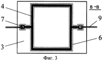
Фиг.3. ММЭД-1 - сечение изображения на Фиг.2 по плоскости В-В.Figure 3. MMED-1 is a cross-section of the image in figure 2 along the plane BB.
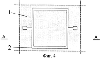
Фиг.4. Приборный кристалл ММЭД-1 после формирования окна в пленке SiO2 - вид на кристалл со стороны, обращенной к концентратору. (Пунктирные линии на этой и нижеследующих фигурах обозначают плоскости разделения технологической пластины на приборные кристаллы.)Figure 4. The instrumented crystal MMED-1 after the formation of a window in a SiO 2 film is a view of the crystal from the side facing the concentrator. (The dashed lines in this and the following figures indicate the plane of separation of the process plate into instrument crystals.)
Фиг.5. Приборный кристалл ММЭД-1 после формирования окна в пленке SiO2 - сечение изображения на Фиг.4 по плоскости А-А.Figure 5. The instrumented crystal MMED-1 after the formation of the window in the SiO 2 film is a section of the image in figure 4 along the plane aa.
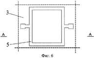
Фиг.6. Приборный кристалл ММЭД-1 после формирования тензорезистора р+-типа проводимости и маски из пленки SiO2 - вид на кристалл со стороны, обращенной к концентратору.6. The instrumented crystal MMED-1 after the formation of a p + type conductivity strain gauge and a mask from a SiO 2 film is a view of the crystal from the side facing the concentrator.
Фиг.7. Приборный кристалл ММЭД-1 после формирования тензорезистора p+-типa проводимости и маски из пленки SiO2 - сечение изображения на Фиг.6 по плоскости А-А.7. The instrumented crystal MMED-1 after the formation of a p + type conductivity strain gauge and a mask from a SiO 2 film — the image cross section in FIG. 6 along plane AA.
Фиг.8. Приборный кристалл ММЭД-1 после формирования выступа в виде замкнутой рамки - вид со стороны, обращенной к концентратору.Fig. 8. Instrument crystal MMED-1 after the formation of the protrusion in the form of a closed frame - view from the side facing the hub.
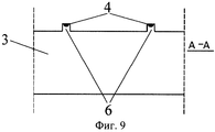
Фиг.9. Приборный кристалл ММЭД-1 после формирования выступа в виде замкнутой рамки - сечение изображения на Фиг.8 по плоскости А-А.Fig.9. The instrumented crystal MMED-1 after the formation of the protrusion in the form of a closed frame is a section of the image in Fig.8 along the plane AA.
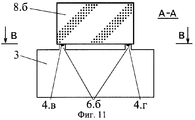
Фиг.10. ММЭД-2 - вид со стороны концентратора.Figure 10. MMED-2 - view from the hub.
Фиг.11. ММЭД-2 - сечение изображения на Фиг.10 по плоскости А-А.11. MMED-2 - section of the image in Figure 10 along the plane AA.
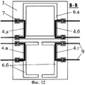
Фиг.12. ММЭД-2 - сечение изображения на Фиг.11 по плоскости В-В.Fig. 12. MMED-2 is a cross-section of the image in figure 11 along the plane BB.
Фиг.13. Приборный кристалл ММЭД-2 после формирования окон в пленке SiO2 - вид на кристалл со стороны, обращенной к концентратору.Fig.13. The instrumented crystal MMED-2 after the formation of windows in the SiO 2 film is a view of the crystal from the side facing the concentrator.
Фиг.14. Приборный кристалл ММЭД-2 после формирования окон в пленке SiO2 - сечение изображения на Фиг.13 по плоскости А-А.Fig.14. The instrumented crystal MMED-2 after the formation of windows in a SiO 2 film is a section of the image in Fig. 13 along the plane AA.
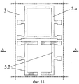
Фиг.15. Приборный кристалл ММЭД-2 после формирования тензорезисторов р+-типа проводимости и масок из пленки SiO2 - вид на кристалл со стороны, обращенной к концентратору.Fig.15. The instrumented crystal MMED-2 after the formation of p - type conductivity strain gauges and masks from a SiO 2 film is a view of the crystal from the side facing the concentrator.
Фиг.16. Приборный кристалл ММЭД-2 после формирования тензорезисторов р+-типа проводимости и масок из пленки SiO2 - сечение изображения Фиг.15 по плоскости А-А.Fig.16. The instrumented crystal MMED-2 after the formation of p - type conductivity strain gauges and masks from a SiO 2 film is a cross-section of the image of Fig. 15 along the plane AA.
Фиг.17. Приборный кристалл ММЭД-2 после формирования выступов - вид со стороны, обращенной к концентратору.Fig.17. The instrumented crystal MMED-2 after the formation of the protrusions is a view from the side facing the concentrator.
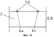
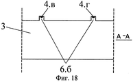
Фиг.18. Приборный кристалл ММЭД-2 после формирования выступов - сечение изображения на Фиг.17 по плоскости А-А.Fig. 18. The instrumented crystal MMED-2 after the formation of the protrusions is a section of the image in Fig.17 along the plane AA.
ММЭД-1 содержит (фиг.1 - 3) полупроводниковый кристалл 3 из кремния n-типа проводимости, упругий элемент 6 в виде выступа на поверхности кристалла в форме замкнутой рамки, чувствительный элемент 4, сформированный в выступе в виде тензорезистора из кремния p+-типа проводимости, соединенный с омическими контактными площадками 7, концентратор 8 в виде жесткой пластины из боросиликатного стекла, согласованного с кремнием по коэффициенту температурного расширения, соединенный жестко и вакуумно-плотно с поверхностью упругого элемента - выступа 6 методом электростатической сварки, микропроволочные электровыводы 9, соединенные с контактными площадками 7 и предназначенные для коммутации чувствительного элемента - тензорезистора 4 с электронной схемой (на фиг.1 - 3 не изображена), служащей для преобразования изменений сопротивления чувствительного элемента - тензорезистора в эквивалентный электрический сигнал. Вакуумно-плотное соединение упругого элемента - выступа, выполненного в виде замкнутой рамки 6, с концентратором - пластиной 8 образует полость, изолированную от среды измеряемого давления.MMED-1 contains (Figs. 1-3) a n-type
ММЭД-1 (фиг.1 - 3) работает следующим образом. ММЭД-1 размещают в полости корпуса измерительного преобразователя давления, в которой действует измеряемое давление. Микропроволочные электровыводы 9 коммутируют с электронной схемой. Электронная схема подает электрический сигнал смещения на чувствительный элемент - тензорезистор 4. Измеряемое давление через жесткий концентратор 8 передается в виде усилия на упругий элемент - выступ 6, что приводит к изменению сопротивления чувствительного элемента - тензорезистора 4 вследствие эффекта поперечного пьезосопротивления р+-кремния. Электронная схема преобразует изменение сопротивления чувствительного элемента - тензорезистора 4 в эквивалентный электрический сигнал, по которому судят об измеряемом давлении.MMED-1 (figure 1 - 3) works as follows. MMED-1 is placed in the cavity of the housing of the measuring pressure transducer, in which the measured pressure acts. Microwire
ММЭД-2 содержит (фиг.10 - 12) полупроводниковый кристалл 3 из кремния n-типа проводимости, два выступа на его поверхности, один из которых (6.а) выполнен в виде замкнутой рамки, а другой (6.б) в виде рамки, содержащей два разрыва, чувствительные элементы в виде четырех тензорезисторов из кремния р+-типа проводимости (4.а, 4.б, 4.в, 4.г), сформированных попарно в каждом из упомянутых выступов, омические контактные площадки 7 к тензорезисторам, микропроволочные электровыводы 9, соединенные с контактными площадками 7 и предназначенные для коммутации тензорезисторов с электронной схемой (на фиг.10 - 12 не изображена), служащей для преобразования изменений сопротивлений тензорезисторов в эквивалентный электрический сигнал, концентратор в виде жесткой пластины 8.а из боросиликатного стекла, согласованного с кремнием по коэффициенту температурного расширения, жестко и вакуумно-плотно соединенный с поверхностью выступа 6.а методом электростатической сварки, пластину 8.б из такого же стекла, идентичную по исполнению пластине 8.а и жестко соединенную с поверхностью выступа 6.б методом электростатической сварки. Вакуумно-плотное соединение упругого элемента - выступа, выполненного в виде замкнутой рамки 6.а, с концентратором - пластиной 8.а образует полость, изолированную от среды измеряемого давления. Наличие разрывов в выступе 6.б обеспечивает проникновение среды давления в полость под пластиной 8.б. Сопротивления тензорезисторов 4.а, 4.б, 4.в, 4.г имеют идентичную зависимость от температуры благодаря идентичному исполнению обеих твердотельных пластин и одинаковости геометрических размеров обоих выступов.MMED-2 contains (Figs. 10-12) a
ММЭД-2 (фиг.10 - 12) работает следующим образом. ММЭД-2 размещают в полости корпуса измерительного преобразователя давления, в которой действует измеряемое давление. Микропроволочные электровыводы 9 коммутируют с электронной схемой. Электронная схема соединяет тензорезисторы 4.а, 4.б, 4.в, 4.г в мост Уитстона так, что тензорезисторы 4.а и 4.б образуют его противоположные плечи, подает электрическое питание на одну из диагоналей моста и регистрирует разность потенциалов в другой диагонали моста (регистрирует разбаланс моста). Измеряемое давление через жесткий концентратор 8.а передается в виде усилия на упругий элемент - выступ 6.а, что приводит к изменению сопротивлений тензорезисторов 4.а, 4.б вследствие эффекта поперечного пьезосопротивления р+-кремния и к изменению разбаланса моста, поскольку сопротивления тензорезисторов 4.в, 4.г не зависят от измеряемого давления. В то же время изменение температуры не изменяет разбаланс моста, поскольку сопротивления тензорезисторов 4.а, 4.б, 4.в, 4.г имеют одинаковую зависимость от температуры. По изменению разбаланса моста судят об измеряемом давлении.MMED-2 (figure 10 - 12) works as follows. MMED-2 is placed in the cavity of the housing of the measuring pressure transducer, in which the measured pressure acts. Microwire
Предложенное исполнение ММЭД-1 может быть реализовано в излагаемой ниже технологической последовательности. На поверхности технологической пластины кремния n-типа проводимости формируется первый сплошной слой окисла SiQ2 1 (фиг.4), в котором вскрываются окна - по одному окну 2 на каждом приборном кристалле кремния 3 в виде замкнутой рамки, связанной дорожками с двумя площадками, расположенными за пределами рамки (фиг.4, 5). Проводится ионная имплантация бора, удаление первого слоя SiO2, формирование второго сплошного слоя SiO2 и последующая термическая разгонка бора. В итоге в технологической пластине кремния на ее участках, находившихся в окнах 2 первого слоя SiO2 1 (фиг.4, 5), образуются области p+-типа проводимости 4 (зачерненные области на фиг.1 - 3, фиг.7 - 9), электрически изолированные от технологической пластины p+-n переходом. Из второго слоя SiO2 формируются маски - по одной маске 5 на каждом приборном кристалле кремния 3 (фиг.6, 7) в виде замкнутой рамки, связанной дорожками с двумя площадками, расположенными за пределами рамки. Причем местоположение и размеры масок таковы, что они полностью закрывают рамки, дорожки и площадки р+-типа проводимости (фиг.6, фиг.7). После этого проводится химическое травление технологической пластины на глубину, превышающую толщину дорожек р+-типа проводимости. С поверхности технологической пластины удаляются маски SiO2. В результате на поверхности технологической пластины образуются выступы n-типа проводимости в виде рамок 6, содержащие в своем объеме дорожки р+-типа проводимости 4 (фиг.8, 9), являющиеся тензорезисторами. На участках площадок р+-типа проводимости формируются металлические контактные площадки 7 (фиг.1, 3), служащие омическими контактами к тензорезисторам 4. Технологическая пластина и пластины боросиликатного стекла помещаются на термостол манипулятора, снабженного микрозахватами и микроэлектродными зондами, способными перемещаться по заданной программе. Объем манипулятора вакуумируется, термостол разогревается до +400°С. Стеклянные пластины накладываются поочередно на выступы. Один из электродов прижимается к технологической пластине, другой - к стеклянной пластине. Между электродами подается напряжение 1000 В, индуцирующее электростатическую сварку пластины 8 с поверхностью выступа 6 (фиг.1 - 3). После сварки стеклянных пластин со всеми выступами технологическая пластина извлекается из манипулятора и разделяется на приборные кристаллы 3 (фиг.1). К контактным площадкам 7 привариваются микропроволочные электровыводы 9 (фиг.1).The proposed performance of the MMED-1 can be implemented in the process sequence described below. On the surface of the technological plate of n-type silicon silicon, the first continuous layer of
Предложенное исполнение ММЭД-2 может быть реализовано в излагаемой ниже технологической последовательности. На поверхности технологической пластины кремния n-типа проводимости формируется первый слой окисла SiO2 1 (фиг.13). В этом слое вскрываются окна - четыре окна на каждом приборном кристалле 3 в виде фигур из С-образных дорожек 2.а, 2.б, 2.в, 2.г, заканчивающихся площадками (фиг.13, 14). Проводится ионная имплантация бора, удаление первого слоя SiO2, формирование второго слоя SiO2 и последующая термическая разгонка бора. В итоге в технологической пластине кремния на ее участках, находившихся в окнах 2.а, 2.б, 2.в, 2.г первого слоя SiO2 (фиг.13), образуются области p+-типа проводимости 4.а, 4.б, 4.в, 4.г (зачерненные области на фиг.10 - 12, фиг.16 - 18), электрически изолированные от технологической пластины р+-n переходом. Из второго слоя SiO2 формируются маски в виде двух рамок на каждом приборном кристалле 3 (фиг.15, 16), одна из которых (5.а) замкнута, а вторая (5.б) содержит разрывы, и восьми площадок, соединенных дорожками с рамками. Причем местоположение и размеры масок таковы, что они полностью закрывают дорожки 4.а, 4.б, 4.в, 4.г и площадки р+-типа проводимости так, что под каждой маской оказывается по две дорожки р+-типа проводимости (фиг.15, 16). После этого проводится химическое травление технологической пластины на глубину, превышающую толщину дорожек p+-типа проводимости. Затем с поверхности технологической пластины удаляются маски SiO2. В результате на поверхности технологической пластины образуются выступы в виде рамок n-типа проводимости 6.а и 6.б, содержащие в своем объеме дорожки р+-типа проводимости 4.а, 4.б и 4.в, 4.г (фиг.17, 18), являющиеся тензорезисторами. На участках площадок р+-типа проводимости формируются металлические контактные площадки 7 (фиг.10, 12), служащие омическими контактами к тензорезисторам 4.а, 4.б, 4.в, 4.г. Технологическая пластина и пластины боросиликатного стекла помещаются на термостол манипулятора. Объем манипулятора вакуумируется, термостол разогревается до +400°С. Две стеклянные пластины накладываются на выступы технологической пластины, принадлежащие одному приборному кристаллу. Один из электродов прижимается к технологической пластине, два других - к стеклянным пластинам. Между электродом, прижатым к технологической пластине, и каждым из электродов, прижатых к стеклянным пластинам, подается напряжение 1000 В, индуцирующее одновременную электростатическую сварку стеклянных пластин 8.а и 8.б с выступами 6.а и 6.б (фиг.10). После сварки стеклянных пластин со всеми выступами технологическая пластина извлекается из манипулятора и разделяется на приборные кристаллы. К контактным площадкам 7 привариваются микропроволочные электровыводы 9 (фиг.10).The proposed execution of the MMED-2 can be implemented in the process sequence described below. On the surface of the technological plate of silicon n-type conductivity, the first layer of
С целью снижения механических напряжений в предложенных ММЭД концентратор может быть выполнен в виде жесткой кремниевой пластины n-типа проводимости, соединяемой с выступом по одной из известных технологий жесткого соединения кремния с кремнием.In order to reduce mechanical stresses in the proposed MWED, the concentrator can be made in the form of a rigid n-type silicon wafer connected to a protrusion using one of the known technologies for rigid bonding of silicon with silicon.
С целью повышения стабильности сопротивлений тензорезисторов, способствующей долговременной стабильности метрологических характеристик ММЭД, могут быть использованы технологические пластины кремния n-типа проводимости, на поверхности которых содержатся два последовательно сменяющих друг друга слоя: слой р+-типа проводимости и слой n-типа проводимости. (Эти слои могут быть сформированы, например, методом эпитаксии.) Тензорезистивный слой р+-типа проводимости, попадающий в выступ, оказывается изолированным сверху и снизу р+-n переходами. Изоляция же тензорезисторов и p+-n переходов со стороны боковых поверхностей выступов может быть обеспечена окислением кремния в атмосфере сухого кислорода.In order to increase the resistance resistance of strain gauges, which contributes to the long-term stability of the metrological characteristics of MMED, technological n-type silicon wafers can be used, on the surface of which there are two successively alternating layers: a p + type conductivity layer and an n-type conductivity layer. (These layers can be formed, for example, by the method of epitaxy.) The tensoresistive layer of the p + type of conductivity falling into the protrusion is isolated by p + –n junctions above and below. Isolation of strain gauges and p + -n junctions from the side of the lateral surfaces of the protrusions can be ensured by oxidation of silicon in an atmosphere of dry oxygen.
Предложенные варианты исполнения ММЭД содержат только жесткие и жестко соединенные между собой конструктивные элементы, выполненные из материалов, в которых затруднено развитие пластических деформаций при длительных механических воздействиях (монокристаллический кремний, боросиликатное стекло). Благодаря этому достигается высокая точность измерения постоянных давлений. Практические испытания представительных выборок ММЭД-1 и ММЭД-2 на воздействие постоянных давлений с длительной выдержкой при давлении, превышающем верхний предел диапазона измерений, показали, что суммарная погрешность повторяемости и вариации не выше 0,1%. Высокой точности измерения статических давлений ММЭД-2 способствует также высокая температурная стабильность исходного разбаланса тензорезистивного моста (высокая температурная стабильность “нуля”), обусловленная идентичностью конструктивного и технологического исполнения концентраторов - пластин, упругих элементов - выступов и чувствительных элементов - тензорезисторов. Действительно, если в мембранных МЭД разность коэффициентов температурного расширения кремния и контактирующих с ним материалов ведет к термомеханическим деформациям мембраны и температурному уходу “нуля” тензорезистивного моста, поскольку сопротивления тензорезисторов в сопряженных плечах моста при деформации мембраны изменяются с разными знаками, то в ММЭД-2 термомеханические деформации обоих выступов одинаковы и все сопротивления тензорезистивного моста изменяются при изменении температуры с одинаковыми знаками.The proposed versions of the MMED contain only rigid and rigidly interconnected structural elements made of materials in which the development of plastic deformations during prolonged mechanical stresses is difficult (monocrystalline silicon, borosilicate glass). Due to this, a high accuracy of measuring constant pressures is achieved. Practical tests of representative samples of MMED-1 and MMED-2 on the effect of constant pressures with long exposure at a pressure exceeding the upper limit of the measurement range showed that the total error in repeatability and variation is not higher than 0.1%. The high temperature stability of the initial imbalance of the strain gauge bridge (high temperature stability of “zero”), due to the identity of the structural and technological design of the concentrators — plates, elastic elements — protrusions and sensitive elements — strain gauges, also contributes to the high accuracy of measuring static pressures. Indeed, if in the membrane DER, the difference in the coefficients of thermal expansion of silicon and the materials in contact with it leads to thermomechanical deformations of the membrane and the temperature “zero” of the strain gage bridge, since the resistance of the strain gages in the conjugate arms of the bridge change with different signs, then in MEDED-2 the thermomechanical deformations of both protrusions are the same and all the resistances of the strain gauge bridge change with temperature with the same signs.
Высокая точность измерения постоянных давлений сочетается в ММЭД с высоким быстродействием. Линейная частота собственных резонансных механических колебаний концентратора на упругом элементе (в понимании стеклянной пластины массой, а кремниевого выступа - пружиной) без учета потерь колебательной энергии на трение в окружающей среде и на внутреннее трение может быть определена известным соотношением ν=(1/2π)(G/m)1/2. Здесь: m - масса пластины, задаваемая плотностью стекла (≈3 мг/мм3) и объемом пластины (в реальных примерах исполнения 0,40×0,40×0,40 мм3); G - жесткость выступа, задаваемая соотношением G≈(Е×s2)/(h×S), где Е - модуль упругости кремния (Е≈105 МПа), S - площадь полости, ограниченная рамкой-выступом (S≈0,350×0,350 мм2), s - площадь рамки-выступа (s≈4×0,350×0,002 мм2), h - высота рамки-выступа (h=0,0015 мм). Получаемое из расчета значение ν≈2 МГц служит признаком работоспособности ММЭД в частотном диапазоне давлений от статики до ≈500 кГц. Возможность задания размеров выступов-рамок с литографической точностью способствует высокой технологической воспроизводимости ММЭД по чувствительности к давлению, что открывает дорогу к отказу от индивидуальной калибровки и к бескалибровочной взаимозамене ММЭД в эксплуатации при не слишком высоких требованиях к точности измерения. Изменением размеров выступов-рамок можно в широких пределах изменять коэффициент мультипликации давления и, следовательно, диапазон измерения и чувствительность ММЭД к давлению. Технология изготовления предложенных ММЭД содержит только стандартные операции групповой планарной технологии кремниевых приборов: одностороннюю литографию, формирование окисных пленок, ионную имплантацию, термические отжиги, поверхностное химическое травление кремния, напыление металлов, автоматизированную сварку кремния со стеклом и микропроволочных электровыводов с металлизированными контактными площадками. Это обеспечивает высокую надежность и низкую себестоимость ММЭД.High accuracy of constant pressure measurement is combined with high speed in the EDME. The linear frequency of natural resonant mechanical vibrations of a concentrator on an elastic element (in the sense of a glass plate is mass and a silicon protrusion is a spring) without taking into account the vibrational energy losses due to friction in the environment and internal friction can be determined by the known relation ν = (1 / 2π) ( G / m) 1/2 . Here: m is the mass of the plate, specified by the density of the glass (≈3 mg / mm 3 ) and the volume of the plate (in real examples 0.40 × 0.40 × 0.40 mm 3 ); G - protrusion stiffness, defined by the relation G≈ (E 2 × s) / (h × S), where E - silicon modulus (MPa E≈10 5), S - area of the cavity bounded by the frame-protrusion (S≈0,350 × 0.350 mm 2 ), s is the area of the protrusion frame (s≈4 × 0.350 × 0.002 mm 2 ), h is the height of the protrusion frame (h = 0.0015 mm). The value ν≈2 MHz obtained from the calculation serves as a sign of the operational efficiency of the MWED in the frequency range of pressures from statics to ≈500 kHz. The ability to set the size of the protrusions-frames with lithographic accuracy contributes to the high technological reproducibility of the MWED by pressure sensitivity, which opens the way to the rejection of individual calibration and to calibration without interchange of MMED in operation with not too high requirements for measurement accuracy. By varying the size of the protrusions-frames, it is possible to widely vary the coefficient of pressure multiplication and, consequently, the measurement range and the sensitivity of the EDM to pressure. The manufacturing technology of the proposed MWED contains only standard operations of the group planar technology of silicon devices: single-sided lithography, formation of oxide films, ion implantation, thermal annealing, surface chemical etching of silicon, metal sputtering, automated welding of silicon with glass and microwire electrical leads with metallized contact pads. This provides high reliability and low cost MMED.
Claims (2)
Priority Applications (2)
| Application Number | Priority Date | Filing Date | Title |
|---|---|---|---|
| RU2003125016/28A RU2247342C1 (en) | 2003-08-11 | 2003-08-11 | Multiplicative microelectronic pressure transducer |
| PCT/RU2004/000304 WO2005015147A1 (en) | 2003-08-11 | 2004-08-06 | Multiplicative microelectronic pressure gauge |
Applications Claiming Priority (1)
| Application Number | Priority Date | Filing Date | Title |
|---|---|---|---|
| RU2003125016/28A RU2247342C1 (en) | 2003-08-11 | 2003-08-11 | Multiplicative microelectronic pressure transducer |
Publications (2)
| Publication Number | Publication Date |
|---|---|
| RU2003125016A RU2003125016A (en) | 2005-02-20 |
| RU2247342C1 true RU2247342C1 (en) | 2005-02-27 |
Family
ID=34132470
Family Applications (1)
| Application Number | Title | Priority Date | Filing Date |
|---|---|---|---|
| RU2003125016/28A RU2247342C1 (en) | 2003-08-11 | 2003-08-11 | Multiplicative microelectronic pressure transducer |
Country Status (2)
| Country | Link |
|---|---|
| RU (1) | RU2247342C1 (en) |
| WO (1) | WO2005015147A1 (en) |
Cited By (1)
| Publication number | Priority date | Publication date | Assignee | Title |
|---|---|---|---|---|
| WO2011078715A1 (en) * | 2009-12-22 | 2011-06-30 | Pivonenkov Boris Ivanovisch | Method for measuring physical values using piezoresistive transducers and transducer |
Family Cites Families (5)
| Publication number | Priority date | Publication date | Assignee | Title |
|---|---|---|---|---|
| JPS5828876A (en) * | 1981-08-12 | 1983-02-19 | Mitsubishi Electric Corp | Semiconductor pressure sensor |
| JPH073380B2 (en) * | 1983-05-31 | 1995-01-18 | 株式会社日立製作所 | Integrated pressure sensor |
| SU1553856A1 (en) * | 1987-07-15 | 1990-03-30 | Предприятие П/Я М-5696 | Pressure pickup |
| RU2047113C1 (en) * | 1993-02-04 | 1995-10-27 | Научно-исследовательский институт физических измерений | Semiconductor pressure transducer |
| RU2169912C1 (en) * | 2000-03-30 | 2001-06-27 | Московский государственный институт электронной техники (технический университет) | Microelectron pressure transducer |
-
2003
- 2003-08-11 RU RU2003125016/28A patent/RU2247342C1/en not_active IP Right Cessation
-
2004
- 2004-08-06 WO PCT/RU2004/000304 patent/WO2005015147A1/en active Application Filing
Non-Patent Citations (1)
| Title |
|---|
| ВЯТКИН А.П., КРИВОРОТОВ Н.П., ЩЕГОЛЬ С.С. Высокочувствительный быстродействующий датчик давления с туннельным диодом. ПТЭ, 1988, №1, с.186-188. * |
Cited By (1)
| Publication number | Priority date | Publication date | Assignee | Title |
|---|---|---|---|---|
| WO2011078715A1 (en) * | 2009-12-22 | 2011-06-30 | Pivonenkov Boris Ivanovisch | Method for measuring physical values using piezoresistive transducers and transducer |
Also Published As
| Publication number | Publication date |
|---|---|
| WO2005015147A1 (en) | 2005-02-17 |
| RU2003125016A (en) | 2005-02-20 |
Similar Documents
| Publication | Publication Date | Title |
|---|---|---|
| US10768064B2 (en) | MEMS pressure gauge sensor and manufacturing method | |
| US11226251B2 (en) | Method of making a dual-cavity pressure sensor die | |
| CN109786422B (en) | Piezoelectric excitation tension type silicon micro-resonance pressure sensor chip and preparation method thereof | |
| Niu et al. | Design optimization of high pressure and high temperature piezoresistive pressure sensor for high sensitivity | |
| US11255740B2 (en) | Pressure gauge chip and manufacturing process thereof | |
| CN101858929B (en) | Capacitive micro-acceleration sensor with symmetrically combined elastic beam structure and production method thereof | |
| He et al. | A silicon directly bonded capacitive absolute pressure sensor | |
| US8384170B2 (en) | Pressure sensor | |
| CA2017704A1 (en) | Laminated semiconductor sensor with vibrating element and associated method and product | |
| CN108254106A (en) | A kind of silicon silica glass silicon four-layer structure resonant mode MEMS pressure sensor preparation method | |
| CN112284607B (en) | Cross island high-temperature-resistant corrosion-resistant pressure sensor chip and preparation method thereof | |
| CN109212264A (en) | The electric acceleration transducer of the shearing flexure of annular and stepped construction acceleration transducer | |
| CN107976274B (en) | Pressure detection device and method based on synchronous resonance | |
| RU2247342C1 (en) | Multiplicative microelectronic pressure transducer | |
| JPH01152369A (en) | Capacity type acceleration sensor | |
| Veske et al. | Characterization of packaging stress with a capacitive stress sensor array | |
| Zhang et al. | A high-accuracy multi-element silicon barometric pressure sensor | |
| CN113465791B (en) | Resonant pressure sensor and preparation method thereof | |
| RU2284613C1 (en) | Semiconductor pressure transducer and its manufacturing process | |
| Lin et al. | A Bulk-Type High-Pressure MEMS Pressure Sensor With Dual-Cavity Induced Mechanical Amplification | |
| Qaradaghi et al. | Frequency output MEMS resonator on membrane pressure sensors | |
| Jiang et al. | Oil-filled Isolated high pressure sensor for high temperature application | |
| Ghanam et al. | Full Silicon Capacitive Force Sensors with Low Temperature Drift and High Temperature Range | |
| CN216593886U (en) | Micro-electromechanical resonance type pressure sensitive structure | |
| CN112284606B (en) | T-shaped cross beam cross island membrane pressure sensor chip and preparation method thereof |
Legal Events
| Date | Code | Title | Description |
|---|---|---|---|
| MM4A | The patent is invalid due to non-payment of fees |
Effective date: 20050812 |