RU2024187C1 - Electronic switch - Google Patents
Electronic switchInfo
- Publication number
- RU2024187C1 RU2024187C1 SU4909563A RU2024187C1 RU 2024187 C1 RU2024187 C1 RU 2024187C1 SU 4909563 A SU4909563 A SU 4909563A RU 2024187 C1 RU2024187 C1 RU 2024187C1
- Authority
- RU
- Russia
- Prior art keywords
- resistor
- switch
- bus
- gate
- capacitor
- Prior art date
Links
Images

Landscapes
- Electronic Switches (AREA)
Abstract
Description
Изобретение относится к электронной технике, в частности к импульсной технике, и может быть использовано в модуляторах импульсных передатчиков РЛС. The invention relates to electronic equipment, in particular to pulse technology, and can be used in modulators of pulse radar transmitters.
Известен электронный ключ [1], содержащий ключевой биполярный транзистор, первый и второй управляющие транзисторы, ограничивающий транзистор, резистивный делитель напряжения и два диода. Коллектор ключевого транзистора, эмиттер которого подключен к общей шине, соединен с шиной подключения нагрузки, коллекторы управляющих транзисторов объединены и подключены к положительной шине питания, а между эмиттерами управляющих транзисторов подключен резистивный делитель напряжения, средняя точка которого соединена с базой первого управляющего транзистора, база второго управляющего транзистора соединена с шиной управления. Коллектор ограничивающего транзистора, эмиттер которого соединен с шиной управления, подключен к базе ключевого транзистора, а база ограничивающего транзистора через последовательно соединенные диоды подключена к коллектору ключевого транзистора. Known electronic key [1], containing a key bipolar transistor, the first and second control transistors, a limiting transistor, a resistive voltage divider and two diodes. The collector of the key transistor, the emitter of which is connected to the common bus, is connected to the load connection bus, the collectors of the control transistors are combined and connected to the positive power bus, and a resistive voltage divider is connected between the emitters of the control transistors, the middle point of which is connected to the base of the first control transistor, the base of the second the control transistor is connected to the control bus. The collector of the limiting transistor, the emitter of which is connected to the control bus, is connected to the base of the key transistor, and the base of the limiting transistor is connected through series-connected diodes to the collector of the key transistor.
Недостатками ключа являются малое быстродействие и большая нестабильность длительности выходного импульса, связанная с низким быстродействием высоковольтных биполярных транзисторов, применяемых в качестве ключевого. The disadvantages of the key are the low speed and large instability of the output pulse duration, associated with the low speed of high-voltage bipolar transistors used as the key.
Известен электронный ключ [2], содержащий полевой транзистор со статической индукцией (СИТ) и схему возбуждения, содержащую первый и второй комплементарно соединенные переключающие транзисторы, которые поочередно включаются и выключаются при открывании возбуждающего транзистора. Переключение первого и второго транзисторов вызывает открывание и закрывание СИТ, коллектор первого транзистора подключен к положительной клемме питания. Known electronic key [2], containing a field-effect transistor with static induction (SIT) and an excitation circuit containing the first and second complementary connected switching transistors, which alternately turn on and off when the excitation transistor is opened. Switching the first and second transistors causes the SIT to open and close, the collector of the first transistor is connected to the positive power terminal.
Цель изобретения - повышение быстродействия и стабильности длительности выходного импульса. The purpose of the invention is to increase the speed and stability of the duration of the output pulse.
На фиг. 1 показана схема электронного ключа; на фиг. 2 - диаграмма, где а - импульс запуска, б - импульс запирания, в - напряжение на затворе, г - напряжение на конденсаторе, д - ток затвора. In FIG. 1 shows a diagram of an electronic key; in FIG. 2 is a diagram, where a is the trigger pulse, b is the locking pulse, c is the gate voltage, g is the voltage across the capacitor, d is the gate current.
Электронный ключ содержит СИТ 1, ключи 2 и 3, резисторы 4, 5 и 6, формирователь 7 запирающего импульса, конденсатор 8, диод 9, шину 10 запуска, шины 11 и 12 питания. The electronic switch contains
Электронный ключ работает следующим образом. The electronic key works as follows.
При отсутствии сигнала запуска на шине 10 ключи 2 и 3 закрыты, конденсатор 8 через резисторы 5 и 6 заряжается до напряжения отрицательной шины питания, на затвор СИТ 1 через резистор 5 подается отрицательное напряжение, запирающее СИТ, диод 9 закрыт. Запускающий импульс с шины запуска поступает на управляющий вход ключа 2 (фиг. 2а), ключ 2 открывается, затвор СИТ 1 подключается через резистор 4 к положительной шине 11 питания, напряжение на затворе СИТ 1 становится положительным и равным падению напряжения на открытом р-n-переходе (фиг. 2в), резистор 4 ограничивает прямой ток через затвор СИТ. In the absence of a start signal on bus 10, the
Напряжение на аноде диода 9 за счет напряжения заряда конденсатора 8 становится положительным и приблизительно равным по величине напряжению на отрицательной шине питания. При поступлении положительного напряжения на СИТ 1 он начинает открываться и напряжение на его стоке снижается, пока не станет ниже напряжения на аноде диода 9. Затем диод 9 отпирается и конденсатор 8 через резистор 4 диод 9, сток СИТ 1 начинает разряжаться, при этом прямой ток затвора СИТ 1 уменьшается на величину тока разряда конденсатора 8 (фиг. 2д). В результате процесс отпирания СИТ прекращается и падение напряжения на СИТ стабилизируется на уровне напряжения на конденсаторе 8 (фиг. 2г). Величина конденсатора 8 выбирается такой, чтобы за время действия импульса напряжение заряда на нем изменялось незначительно. The voltage at the anode of the diode 9 due to the charge voltage of the capacitor 8 becomes positive and approximately equal in magnitude to the voltage on the negative power bus. When a positive voltage arrives at
По спаду импульса запуска закрывается ключ 2, формирователь 7 запирающего импульса вырабатывает импульс, который поступает на управляющий вход ключа 3, ключ 3 отпирается и подключает затвор СИТ 1 к отрицательной шине питания через малое внутреннее сопротивление, при этом происходит рассасывание заряда неосновных носителей в затворе СИТ и его запирание. On the decline of the start pulse, the
Ограничение степени отпирания ключевого СИТ путем введения цепи нелинейной отрицательной обратной связи, состоящей из резистора 6, конденсатора 8 и диода 9, уменьшает и стабилизирует величину накопленного заряда неосновных носителей в затворе СИТ 1 и, следовательно, уменьшает время выключения СИТ и повышает стабильность длительности выходного импульса при изменении тока нагрузки и напряжения на положительной шине 12 питания. Limiting the degree of unlocking of the key SIT by introducing a nonlinear negative feedback circuit consisting of a resistor 6, a capacitor 8, and a diode 9 reduces and stabilizes the accumulated charge of minority carriers in the gate of the
Таким образом, уменьшение времени выключения СИТ повышает быстродействие ключа и стабильность длительности выходного импульса. Thus, reducing the time for switching off the SIT increases the key performance and the stability of the output pulse duration.
Так как для восстановления заряда конденсатора 8 необходимо время, в несколько раз превышающее длительность выходного импульса, а на стоке СИТ в открытом состоянии сохраняется значительное остаточное напряжение, то данную схему целесообразно применять в устройствах, работающих с высокой скважностью импульсов и высоким напряжением питания нагрузки, к которым предъявляются жесткие требования к стабильности длительности выходных импульсов, например в модуляторах передатчиков импульсных РЛС. Since it takes time several times longer than the output pulse to restore the charge of capacitor 8, and a significant residual voltage is maintained at the SIT drain in the open state, this circuit should be used in devices operating with high pulse duty cycle and high load supply voltage, to which have strict requirements for the stability of the duration of the output pulses, for example, in modulators of pulse radar transmitters.
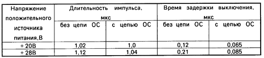
Данное техническое решение проверялось на макете импульсного передатчика, в ключе применялись три параллельно включенных СИТ КП802А. Нагрузкой ключа является импульсный трансформатор с коэффициентом трансформации 6, 2, во вторичную обмотку которого включен магнетрон со следующими параметрами: напряжение анода 2, 4 кВ, ток анода 1,5 А. В макете использовались напряжение отрицательной шины питания -27В - напряжение отрицательной шины питания и напряжение положительной шины питания - +20-+28 В. Режим работы ключа: напряжение питания нагрузки +400 В, ток в нагрузке 10А, длительность импульса 1 мкс, частота следования импульсов 1 кГц. This technical solution was tested on the model of a pulse transmitter; three SIT KP802A connected in parallel were used in the key. The key load is a pulse transformer with a transformation ratio of 6, 2, the magnetron with the following parameters is included in the secondary winding: anode voltage of 2.4 kV, anode current of 1.5 A. The negative supply bus voltage was -27V - the negative supply bus voltage and the voltage of the positive power bus is + 20- + 28 V. The operating mode of the switch is: power supply voltage + 400 V, current in the load 10A,
При испытаниях проверялись длительность выходного импульса огибающей СВЧ-сигнала и время задержки включения ключа относительно спада запускающего импульса при изменении напряжения положительного источника питания от 20 до 28 В. Испытания проводились при подключенной и отключенной цепи нелинейной отрицательной обратной связи. Результаты испытания приведены в таблице. During the tests, the duration of the output pulse of the envelope of the microwave signal and the delay time of the key switch on relative to the drop in the triggering pulse when the voltage of the positive power supply was changed from 20 to 28 V. The tests were carried out with the non-linear negative feedback circuit connected and disconnected. The test results are shown in the table.
Таким образом, после введения цепи нелинейной отрицательной обратной связи суммарная нестабильность длительности импульса уменьшилась в 2,5 раза, время задержки выключения - в 2-2,4 раза, нестабильность времени задержки выключения - в 4,5 раза. Thus, after the introduction of the nonlinear negative feedback circuit, the total instability of the pulse duration decreased by 2.5 times, the turn-off delay time - by 2-2.4 times, the turn-off delay time instability - by 4.5 times.
Сопоставительный анализ с прототипом показал, что предлагаемый ключ отличается наличием отрицательной обратной связи, образованной резистором, диодом и конденсатором, и связями между ними и СИТ. Это позволяет сделать вывод о соответствии предлагаемого технического решения критерию "новизна". Comparative analysis with the prototype showed that the proposed key is characterized by the presence of negative feedback formed by a resistor, diode and capacitor, and the connections between them and the SIT. This allows us to conclude that the proposed technical solution meets the criterion of "novelty."
Сравнение предлагаемого технического решения с другими решениями в данной области техники не выявило признаки, отличающие заявляемое решение от прототипа. Вместе с тем новая совокупность признаков проявляет новые свойства - высокое быстродействие и высокую стабильность длительности выходного импульса. Это позволяет сделать вывод о соответствии предлагаемого технического решения критерию изобретения "существенные отличия". Comparison of the proposed technical solutions with other solutions in this technical field did not reveal signs that distinguish the claimed solution from the prototype. At the same time, a new set of features exhibits new properties - high speed and high stability of the output pulse duration. This allows us to conclude that the proposed technical solution meets the criteria of the invention "significant differences".
Claims (1)
Priority Applications (1)
| Application Number | Priority Date | Filing Date | Title |
|---|---|---|---|
| SU4909563 RU2024187C1 (en) | 1991-02-07 | 1991-02-07 | Electronic switch |
Applications Claiming Priority (1)
| Application Number | Priority Date | Filing Date | Title |
|---|---|---|---|
| SU4909563 RU2024187C1 (en) | 1991-02-07 | 1991-02-07 | Electronic switch |
Publications (1)
| Publication Number | Publication Date |
|---|---|
| RU2024187C1 true RU2024187C1 (en) | 1994-11-30 |
Family
ID=21559612
Family Applications (1)
| Application Number | Title | Priority Date | Filing Date |
|---|---|---|---|
| SU4909563 RU2024187C1 (en) | 1991-02-07 | 1991-02-07 | Electronic switch |
Country Status (1)
| Country | Link |
|---|---|
| RU (1) | RU2024187C1 (en) |
Cited By (1)
| Publication number | Priority date | Publication date | Assignee | Title |
|---|---|---|---|---|
| RU2563155C1 (en) * | 2014-12-25 | 2015-09-20 | Федеральное государственное унитарное предприятие "Научно-производственный центр автоматики и приборостроения имени академика Н.А. Пилюгина" (ФГУП "НПЦАП") | Self-locking electronic switch |
-
1991
- 1991-02-07 RU SU4909563 patent/RU2024187C1/en active
Non-Patent Citations (2)
| Title |
|---|
| 1. Европейский патент ЕПВ N 0409747, кл. H 03K 17/687, 1990. * |
| 2. Заявка Японии N 61-976, кл. H 03K 17/687, 1986. * |
Cited By (1)
| Publication number | Priority date | Publication date | Assignee | Title |
|---|---|---|---|---|
| RU2563155C1 (en) * | 2014-12-25 | 2015-09-20 | Федеральное государственное унитарное предприятие "Научно-производственный центр автоматики и приборостроения имени академика Н.А. Пилюгина" (ФГУП "НПЦАП") | Self-locking electronic switch |
Similar Documents
| Publication | Publication Date | Title |
|---|---|---|
| US3983461A (en) | Ignition pulse generator | |
| US3257583A (en) | Impulse generating circuit for intermittent discharge machining | |
| US3636476A (en) | Solid-state double resonant pulser | |
| RU2024187C1 (en) | Electronic switch | |
| US3938027A (en) | Electrical thyristor circuit | |
| RU2034400C1 (en) | Pulse modulator | |
| SU1368970A1 (en) | Signal shaper | |
| RU2079967C1 (en) | Pulse modulator | |
| Naito et al. | A high voltage pulse generator using avalanche‐mode thyristors | |
| SU1485394A1 (en) | Thyristor switch | |
| SU611295A1 (en) | Current shaper | |
| SU1427351A1 (en) | Pulsed stabilizer | |
| SU1758852A1 (en) | Former of high-voltage pulses of special form | |
| RU2185021C1 (en) | Totem-pole high-voltage pulse generator | |
| SU1383479A1 (en) | Gate device | |
| RU2013860C1 (en) | Magnetic-transistor switch | |
| SU745460A1 (en) | Apparatus for electric fishing | |
| SU527816A1 (en) | Blocking generator | |
| SU1667187A1 (en) | Device for protection against short-circuits in power network | |
| SU1644339A1 (en) | Inverter with separate excitation | |
| SU1251248A1 (en) | Device for controlling thyristor | |
| SU809505A1 (en) | Pulse generator | |
| SU1252922A1 (en) | Pulse generator | |
| SU458090A1 (en) | Pulse shaper | |
| SU1721750A1 (en) | Dc converter |