KR970001620B1 - Electrical-terminal pin with compliant portion - Google Patents
Electrical-terminal pin with compliant portion Download PDFInfo
- Publication number
- KR970001620B1 KR970001620B1 KR1019890002333A KR890002333A KR970001620B1 KR 970001620 B1 KR970001620 B1 KR 970001620B1 KR 1019890002333 A KR1019890002333 A KR 1019890002333A KR 890002333 A KR890002333 A KR 890002333A KR 970001620 B1 KR970001620 B1 KR 970001620B1
- Authority
- KR
- South Korea
- Prior art keywords
- coupling
- contact
- hole
- flexible
- pin
- Prior art date
Links
Images


Classifications
-
- H—ELECTRICITY
- H01—ELECTRIC ELEMENTS
- H01R—ELECTRICALLY-CONDUCTIVE CONNECTIONS; STRUCTURAL ASSOCIATIONS OF A PLURALITY OF MUTUALLY-INSULATED ELECTRICAL CONNECTING ELEMENTS; COUPLING DEVICES; CURRENT COLLECTORS
- H01R12/00—Structural associations of a plurality of mutually-insulated electrical connecting elements, specially adapted for printed circuits, e.g. printed circuit boards [PCB], flat or ribbon cables, or like generally planar structures, e.g. terminal strips, terminal blocks; Coupling devices specially adapted for printed circuits, flat or ribbon cables, or like generally planar structures; Terminals specially adapted for contact with, or insertion into, printed circuits, flat or ribbon cables, or like generally planar structures
- H01R12/50—Fixed connections
- H01R12/51—Fixed connections for rigid printed circuits or like structures
- H01R12/55—Fixed connections for rigid printed circuits or like structures characterised by the terminals
- H01R12/58—Fixed connections for rigid printed circuits or like structures characterised by the terminals terminals for insertion into holes
- H01R12/585—Terminals having a press fit or a compliant portion and a shank passing through a hole in the printed circuit board
-
- Y—GENERAL TAGGING OF NEW TECHNOLOGICAL DEVELOPMENTS; GENERAL TAGGING OF CROSS-SECTIONAL TECHNOLOGIES SPANNING OVER SEVERAL SECTIONS OF THE IPC; TECHNICAL SUBJECTS COVERED BY FORMER USPC CROSS-REFERENCE ART COLLECTIONS [XRACs] AND DIGESTS
- Y10—TECHNICAL SUBJECTS COVERED BY FORMER USPC
- Y10T—TECHNICAL SUBJECTS COVERED BY FORMER US CLASSIFICATION
- Y10T29/00—Metal working
- Y10T29/49—Method of mechanical manufacture
- Y10T29/49002—Electrical device making
- Y10T29/49117—Conductor or circuit manufacturing
- Y10T29/49204—Contact or terminal manufacturing
Landscapes
- Multi-Conductor Connections (AREA)
- Coupling Device And Connection With Printed Circuit (AREA)
- Manufacturing Of Electrical Connectors (AREA)
Abstract
내용 없음.No content.
Description
제1도는 본 발명의 단자 핀의 응용을 도시한 몇개의 플레이트된 구멍들을 갖는 인쇄회로기판을 부분적으로 절개시킨 확대 사시도.1 is an enlarged perspective view, partially cut away of a printed circuit board with several plated holes showing the application of the terminal pins of the present invention;
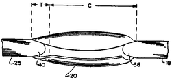
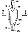
제2도는 본 발명의 단자 핀의 가요성 부분의 측면도.2 is a side view of the flexible portion of the terminal pin of the present invention.
제3도는 제2도에서 축을 중심으로 90o회전시킨 본 발명의 단자 핀의 가요성 부분의 측면도.3 to turn around the axis at a second side view of FIG. 90 o rotation in which the flexible portion of the terminal pin of the present invention.
제4도는 이완된 상태의 본 발명의 단자 핀의 가요성 부분의 단면도.4 is a cross-sectional view of the flexible portion of the terminal pin of the present invention in a relaxed state.
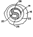
제5도는 플레이트된 구멍내에 삽입된 본 발명의 단자 핀의 가요성 부분의 단면도.5 is a cross-sectional view of the flexible portion of the terminal pin of the present invention inserted into a plated hole.
제6도는 본 발명의 단자 핀의 제조 공정을 도시한 스트립의 정면도.6 is a front view of a strip showing the manufacturing process of the terminal pin of the present invention.
제7도는 본 발명의 단자 핀의 가요성 부분이 S형 단면으로 성형되기 전의 상태를 도시한 부분 정면도.Fig. 7 is a partial front view showing a state before the flexible portion of the terminal pin of the present invention is molded into an S-shaped cross section.
제8도는 제7도의 선 8-8을 따라 취한 단면도.8 is a sectional view taken along line 8-8 of FIG.
제9도는 제7도의 선 9-9를 따라 취한 단면도.9 is a sectional view taken along line 9-9 of FIG.
* 도면의 주요부분에 대한 부호의 설명* Explanation of symbols for main parts of the drawings
10 : 단자 핀 14 : 플레이트된 구멍10: terminal pin 14: plated hole
16 : 인쇄 회로기판 18 : 결합부16: printed circuit board 18: coupling portion
20 : 가요성 부분 22 : 구멍 내부 표면20: flexible part 22: hole inner surface
26 : 아암 38,40 : 보강 돌출부 또는 보강 수단26:
42 : 스트립 52 : 단자 소재42: strip 52: terminal material
54 : 납작부 56 : 날개54: flat 56: wings
본 발명은 회로기판(circuit board)등의 플레이트된 구멍(plated-through hole)내로 삽입되기 위해 적용되는 가요성 부분(compliant portion)을 갖는 전기 단자 핀 및 그 제조 핀 및 그 제조 방법을 관한 것이다.BACKGROUND OF THE INVENTION 1. Field of the Invention The present invention relates to electrical terminal pins having a compliant portion adapted for insertion into plated-through holes, such as circuit boards, and manufacturing pins thereof and methods of manufacturing the same.
가요성 구역 또는 부분을 갖는 단자 핀[때로는 압입 끼움(press-fit)핀이라 불림]은 당 업계에서 30년전부터 공지되어 있다. 가요성 핀들은 인쇄 회로기판의 플레이트된 구멍내로 삽입되도록 설계된다. 핀은 대체로 전기 전도성 요소와 접촉하도록 된 결합부 및 결합부로부터 연장되고 플레이트된 구멍의 내부 표면을 형성하는 도전성 재료와 전기 접촉하는 가요성 부분을 포함한다.Terminal pins (sometimes called press-fit pins) with flexible zones or portions are known in the art for 30 years. Flexible pins are designed to be inserted into plated holes in a printed circuit board. The pin generally includes a coupling portion adapted to contact an electrically conductive element and a flexible portion in electrical contact with a conductive material extending from the coupling portion and forming an inner surface of the plated hole.
대체로, 가요성 핀에서는 보통 이하의 특성들이 바람직하다.In general, the following characteristics are usually desirable in a flexible pin.
1. 고 신뢰성 적용을 위해 납땜은 불필요하다.1. Soldering is unnecessary for high reliability applications.
2. 핀들은 예컨대, 핀들이 플레이트된 구멍으로부터 반복 삽입되는 것과 반복해서 빼내는 작업을 잘 견딜수 있도록 내구성(cyclable)을 가져야 한다. 상기 내구성은 기판과의 임의의 불량 연결을 용이하게 보수할 수 있도록 한다.2. Pins should be cyclable, for example, to withstand the repetitive insertion and retraction of pins from plated holes. The durability makes it easy to repair any bad connections with the substrate.
3. 삽입되는 동안 임의의 손상이 있게되면, 상기 손상은 핀에만 생기고 인쇄 회로기판이나 또는 구멍의 라이닝 전도성 재료에 생겨서는 안된다.3. If there is any damage during insertion, the damage will only occur on the pin and not on the printed circuit board or the lining conductive material of the hole.
4. 탄성 변형 에너지가 핀의 가요성 부분에 대부분 축적되어야 한다.4. The elastic strain energy should be mostly accumulated in the flexible part of the pin.
5. 핀은 다양한 크기를 갖는 구멍에 사용될 수 있어야 한다. 이것은 구멍내에 성형되는 플레이팅 재료의 두께를 변화시켜야 하는 필요성을 제거한다.5. Pins should be able to be used in holes of various sizes. This obviates the need to change the thickness of the plating material to be molded into the hole.
6. 비교적 삽입력이 적게되어 대량 삽입이 가능해야 한다.6. Relatively low insertion force should be possible for mass insertion.
7. 가요성 부분과 플레이트된 구멍 사이의 세팅이 영구적일 경우, 구멍은 더욱 작게 세팅되어야 한다. 이것은 국부 응력(local stress)을 작게하고 인쇄 회로기판을 얇게 할 수 있도록 한다.7. If the setting between the flexible part and the plated hole is permanent, the hole should be set smaller. This makes local stress small and thinner printed circuit boards.
8. 핀의 삽입력은 가능한 한 미는 힘(push out force) 또는 보유력(retention force)과 같아야 한다.8. The insertion force of the pins should be as equal as possible to the push out force or retention force.
9. 가능한 한 가요성 부분의 가장 큰 부분이 가장 큰 수직력으로 플레이트된 구멍의 내부와 맞물려야 한다.9. As much as possible, the largest part of the flexible part shall engage the inside of the plated hole with the greatest vertical force.
10. 일단 플레이트된 구멍에 완전히 삽입되면, 핀의 상부 또는 결합부는 상기 핀이 굴곡되거나 비틀릴 때 파단에 대한 저항성을 가져야 한다.10. Once fully inserted into the plated hole, the top or joint of the pin should be resistant to fracture when the pin is bent or twisted.
11. 핀은 용이하게 제조할 수 있어야 하고, 바람직하게는 대체로 같은 재료 두께를 갖는 편평한 부재(flat blank)를 사용하여야 한다. 현재 시장에서 유통되는 다양한 종류의 가요성 핀 설계들을 상기 목적의 하나 또는 그 이상을 성취하는 데 효과적이다. 그러나, 많은 설계 대안들에서, 하나의 특성에 대한 성능의 향상은 다른 특성에 대한 성능의 감소를 종종 가져올 수 있다.11. Pins should be easy to manufacture and preferably use flat blanks of approximately the same material thickness. Various types of flexible pin designs currently on the market are effective in achieving one or more of the above objectives. However, in many design alternatives, an improvement in performance for one characteristic can often result in a decrease in performance for another characteristic.
상기 특성의 모두를 최상으로 제공하는 가요성 부분의 단면은 대체로 S형 단면이라는 것이 알려졌다. 이러한 유형의 핀들 또는 단자들이 예는 미합중국 특허 제3,907,400호, 미합중국 특허 제4,415,220호 및 1987년 10월 19일로부터 10월 21일까지 펜실베니아주 필라텔피아에서 개최된 제20회 Annual connectors Interconnection Technology Symposium에서 엘렉트로닉 디자인사의 에드워드 에어취. 키이가 발표한 새로운 인발선 가요성 핀의 개발(이하, 키이의 논문이라 한다)에 기재되어 있다.It is known that the cross section of the flexible portion that best provides all of the above properties is generally an S-shaped cross section. Examples of pins or terminals of this type are described in US Patent No. 3,907,400, US Patent No. 4,415,220, and the 20th Annual Connectors Interconnection Technology Symposium held in Philadelphia, Pennsylvania, from October 19 to October 21, 1987. Edward Air smell of Electronic Design. It is described in the development of a new pulley flexible pin published by Kee (hereinafter referred to as Kee's paper).
미합중국 특허 제3,907,400호에는 인쇄 회로기판 구멍을 통하여 삽입되도록 하는 가요성 포스트(compliant type post)가 기재되어 있다. 상기 포스트를 플레이트된 구멍내에 사용하는 것은 기재되어 있지 않다. 포스트의 목적은 인쇄 회로기판의 일측면상의 와이어 랩(wire wrap)을 인쇄 회로기판의 다른 측면상의 다른 구성 요소(예컨대, 다른 와이어 랩)에 연결시키는 것이다.U. S. Patent No. 3,907, 400 describes a compliant type post that allows insertion through a printed circuit board aperture. The use of such posts in plated holes is not described. The purpose of the post is to connect a wire wrap on one side of the printed circuit board to other components (eg, another wire wrap) on the other side of the printed circuit board.
미합중국 특허 제4,415,220호에는 최외측 부분으로부터 타원형 단면으로 종결되는 전이 부분을 통하여 직경이 점차 감소되는 S형 가요성 기재되어 있다(제3도 내지 제6도 참조). 완전히 발달된 부분은 일정한 폭을 갖는다. 일정한 폭 때문에, 삽입시 플레이트된 구멍의 내부에 다항하여 생성되는 수직력에 영향을 미치는 소성 변형이 발생할 수 있다.U. S. Patent No. 4,415, 220 discloses an S-type flexibility in which the diameter gradually decreases through a transition portion ending in an elliptical cross section from the outermost portion (see FIGS. 3-6). The fully developed part has a constant width. Because of the constant width, plastic deformation may occur that affects the normal force generated polynomically inside the plated hole upon insertion.
키이의 논문에는 또한 최외측 부분이 일정한 폭을 가지고 동일한 예기치 않은 소성 변형의 결점을 갖게 되는 S형 가요성 부분이 기재되어 있다. 또한 핀을 인발선(drawn wire)으로 제조하는 제조 공정이 기재되어 있다.Kee's paper also describes an S-type flexible part in which the outermost part has a constant width and has the same unexpected plastic deformation defects. Also described is a manufacturing process for making pins from drawn wires.
이것은 상기 형태의 핀들을 대량 생산하는데에는 비교적 비효율적인 수단이다.This is a relatively inefficient means for mass production of this type of pin.
선행 기술 장치의 결점들을 대체로 이하의 3가지로 분류된다.The shortcomings of the prior art apparatus are generally classified into the following three categories.
1. 가요성 부분이 일정한 폭을 가지기 때문에 삽입 공정 중 소성 변형이 발생한다. 상기 현상은 1981년 5월 11일부터 5월 13일까지 조지아주 아트란타에서 개최된 전자 부품 회의에서 에이엠피 인코포레이티드의 램 고엘이 발표한 압입 끼움(press-frt)기술의 분석이라는 논문(이하, 고엘의 논문이라 한다)의 4페이지의 제5도에 잘 도시되어 있다. 고엘의 논물에서, 대부분의 가요성 핀들의 가요성 부분의 중간부의 삽입하는 동안 내측으로 영구 소성 변형된다. 결과적으로, 플레이트된 구멍의 내부에 대항하여 가장 큰 수직력을 발휘하는 가요성 부분의 중간부가 필요한 가요성은 여전히 보유하고 있으면서도 충분한 힘들을 제공하지는 않게 된다.1. Plastic deformation occurs during the insertion process because the flexible part has a constant width. This is an analysis of press-frt technology presented by Ram Goell of AMP Inc. at the Electronic Components Conference held in Atlanta, Georgia, May 11-May 13, 1981. This is illustrated in Figure 5 on page 4 (hereafter referred to as Goel's paper). In Goel's field, permanent plastic deformation inwards during insertion of the middle portion of the flexible portion of most flexible pins. As a result, the required flexibility in the middle of the flexible part exerting the greatest vertical force against the inside of the plated hole does not provide sufficient force while still retaining it.
2. 가요성 핀에 대한 많은 응용들은 상기 가요성 핀이 플레이트된 구멍내로 삽입된 후에 어느 정도의 굽힘및/또는 비틀림을 지탱할 수 있을 것을 요구한다. 핀의 결합부의 빈번한 굽힘및/또는 비틀림을 인쇄 회로기판의 바로 위에서 핀의 파단을 야기한다. 어떠한 선행 기술도 상기 문제에 대하여 언급하고 있지 않다.2. Many applications for flexible pins require that the flexible pin can bear some degree of bending and / or torsion after being inserted into the plated hole. Frequent bending and / or twisting of the joints of the pins causes the pins to break just above the printed circuit board. No prior art addresses this issue.
3. 사용되는 핀이 어떻게 설계되더라도 용이하게 제조할 수 있어야 한다. 선행 기술의 S형 가요성 핀들의 어떠한 것도 대량 생산가능 설계를 제공하지는 않는다. 그러므로, 본 발명의 주된 목적은 더 큰 접촉 면적과 플레이트된 구멍에 삽입된 후 플레이트된 구멍의 내부에 대향하여 압력을 가하는 더 큰 수직력을 갖는 가요성 부분을 포함하는 전기 핀을 제공하는 것이다. 상기 목적을 위하여, 정기적으로 전도성을 갖는 요소와 접촉하기 위한 결합부와 상기 결합부로부터 연장되고 상기 플레이트된 구멍의 내부 표면을 형성하는 전도성 플레이팅 재료와 전기적 접촉을 이루기 위한 가요성 부분을 포함하고, 상기 가요성 부분이 축 방향으로 제1축단부로부터 플레이트된 구멍의 내부 표면과 접촉부의 축방향 범위를 한정하는 최외측 접촉부까지 테이퍼진 전이부와 회로기판의 플레이트된 구멍내로 삽입되도록 된 단면 S형의 긴 전기 단자 핀에 있어서, 상기 가요성 부분이 전이부로부터 접촉부의 축방향 길이의 중간부를 향하여 점차로 증가되는 폭을 갖는 상기 단면 S형 접촉부를 포함하는 것을 특징으로 하는 전기 단자 핀이 마련된다.3. No matter how the pins used are designed, they should be easy to manufacture. None of the S-type flexible pins of the prior art provide a mass-producible design. It is therefore a primary object of the present invention to provide an electrical pin comprising a larger contact area and a flexible portion having a greater vertical force which is inserted into the plated hole and then pressurized against the interior of the plated hole. For this purpose, it comprises a joining portion for regularly contacting a conductive element and a flexible portion for making electrical contact with a conductive plating material extending from the joining portion and forming an inner surface of the plated hole; A cross-section S such that the flexible portion is inserted into the plated hole of the circuit board and the tapered transition portion from the first axial end to the outermost contact portion defining the axial extent of the inner surface of the plated hole and the contact portion in the axial direction; A long electrical terminal pin of the type, wherein an electrical terminal pin is provided, characterized in that the flexible portion comprises the cross-section S-shaped contact having a width gradually increasing from the transition portion toward the middle portion of the axial length of the contact portion. .
본 발명의 다른 목적은 굽힘/또는 비틀림에 의한 손상에 대해 증가된 저항성을 갖는 전기 단자 핀을 제공하는 것이다. 상기 목적을 위해, 전기적으로 전도성을 갖는 요소와 접촉하기 위한 결합부와 상기 결합부로부터 연장되고 상기 구멍내에 수납되기 위한 구멍 맞물림부를 포함하고, 결함부를 형성하는 재료의 두께가 구멍 맞물림부를 형성하는 재료의 두께보다 크거나 같은 회로기판 내의 구멍내로 삽입되도록 된 긴 전기 단자 핀에 있어서, 횡방향 힘이 결합부에 인가되어 구멍 맞물림부에 대하여 결합부의 굽합을 야기할 때 구멍 맞물림부로부터 결합부가 파단되는 것을 방지하기 위해 결합부와의 접합부로부터 연장되고 구멍 맞물림부의 한쪽에 형성된 보강 수단을 포함하는 것을 특징으로 하는 단자 핀이 마련된다.It is another object of the present invention to provide an electrical terminal pin with increased resistance to damage by bending and / or torsion. For this purpose, a material for forming the hole engagement portion, the thickness of the material forming the defect portion, comprising a coupling portion for contacting an electrically conductive element and a hole engagement portion extending from the coupling portion and received in the hole. In long electrical terminal pins intended to be inserted into a hole in a circuit board that is greater than or equal to the thickness of the connector, the engagement portion breaks from the hole engagement portion when a lateral force is applied to the engagement portion causing the engagement of the engagement portion with respect to the hole engagement portion. A terminal pin is provided which includes reinforcing means extending from the junction with the engaging portion and formed on one side of the hole engaging portion to prevent it.
본 발명의 또다른 목적은 용이하게 대량 생산할 수 있는 상기 형태의 전기 단자 핀을 제공하는 것이다. 상기 목적을 위해, 각각의 핀이 S형 가요성 부분과 결합하는 결합부를 포함하며 평행하게 이격되는, 긴 전기 단자 핀들을 제조하는 방법에 있어서, 핀의 길이 보다 크거나 같은 폭을 갖고 대향된 제1표면 및 제2표면 사이에 형성되고 결합부에 요구되는 두께와 같은 제1의 균일한 두께를 갖는 긴 스트립을 마련하는 단계와, 다수의 평행하고 이격된 단자 부재를 성형하기 위해 길이를 횡단하는 방향으로 스트립을 스탬핑하는 단계와, 가요성 부분의 위치에서 2개의 대향적으로 연장된 테이퍼진 사다리꼴형 날개들을 포함하고 가요성 부분의 축길이와 동일한 구역을 성형하기 위해 부재를 스탬핑하는 단계와 날개들을 단면 S형의 가요성 부분으로 성형하는 단계를 포함하는 것을 특징으로 하는 전기 단자 핀 제조 방법이 마련된다.It is another object of the present invention to provide an electrical terminal pin of the above type which can be easily mass produced. For this purpose, a method of manufacturing long electrical terminal pins, each of which includes a coupling that engages an S-type flexible portion and is spaced in parallel, the opposite agent having a width greater than or equal to the length of the pin and facing each other. Providing an elongated strip formed between the first and second surfaces and having a first uniform thickness equal to the thickness required for the joining portion, and crossing the length to form a plurality of parallel and spaced terminal members; Stamping the strip in the direction, stamping the member to form an area comprising two opposingly extending tapered trapezoidal wings at the location of the flexible portion and forming an area equal to the axial length of the flexible portion and the wing An electrical terminal pin manufacturing method is provided, comprising the step of molding them into a flexible portion of cross-section S type.
이하 도면을 참조하여 본 발명을 상술한다.Hereinafter, the present invention will be described in detail with reference to the accompanying drawings.
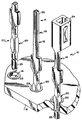
본 발명은 긴 전기 단자 핀(10)에 관한 것이고 상기 핀은 인쇄 회로기판(16)내에 성형된 플레이트된 구멍(14)내로 삽입되도록 된다. 이것은 제1도에 가장 잘 도시되어 있다.The present invention relates to elongated electrical terminal pins 10 which are to be inserted into plated
핀(10)은 전기적으로 전도성을 갖는 요소(도시안됨)와 접촉하기 위한 결합부(18) 및 결합부(18)로부터 하방으로 연장된 가요성 부분(20)을 포함한다. 가요성 부분(20)은 플레이트된 구멍(14)의 내부 표면을 마련하는 전도성 플레이팅 재료(22)와 전기 접촉하도록 한다. 각각의 핀(10)의 결합부(18)은 여러가지 형상을 가질수 있다. 제1도에는 수핀(male pin)(23)의 형태를 갖는 결합부(18)을 도시하고 상기 수핀은 통상적인 암접촉부(female contact)(도시안됨)와 결합하도록 되어 있다. 또한 제1도에서는 통상적인 암접촉부(24)를 구비한 결합부(18)도 도시되어 있고 상기 암접촉부는 다른 수핀(도시안됨)과 결합하도록 되어 있다.The pin 10 includes a
도시한 핀(10)은 가요성 부분(20)으로부터 현수되는 핀 또는 포스트(post)의 형태를 갖는 제2 또는 하부 결합부(25)를 포함한다. 상기 형성에서, 암커넥터 또는 와이어 램이 현수된 포스트(25)에 적용될 수 있다.The illustrated pin 10 includes a second or
제2도를 참조하여 가요성 부분(20)을 자세히 살펴보면, 상기 가요성 부분이 축 방향에서 테이퍼된 도입부(lead-in) 또는 전이부를 포함한다는 것을 알 수 있고 상기 도입부 또는 전이부의 범위는 문자 T로 표기된다. 전이부(T)는 제2도 및 제3도에서 가요성 부분(20)의 제1축 단부로부터 C로 표기된 접촉부를 향하여 연장된다. 접촉부(C)는 축방향으로 전기 및 기계적 접촉을 제공하고 가요성 부분(20)이 플레이트된 구멍(14)의 내부 표면(22)와 접촉하게 된다.Looking closely at the
전이부(T)는 초기에는 플레이트된 구멍(14)의 상부와 맞물린다. 그러나 가요성 부분(20)이 완전히 삽입되면, 접촉부(C)만이 구멍(14)의 내부표면(22)와 맞물리게 된다.The transition portion T initially engages the top of the plated
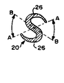
제4도 및 제5도를 참조하여 보면, 가요성 부분(20)의 단면은 대체로 S형이다. S형 단면은 일조의 대향된 대체로 C형의 아암(26)들을 포함한다. 각각의 아암(26)은 단면의 중심을 마련하는 일단부에 서로 결합된다. 각각의 아암(26)의 대항 단부는 내측힘 또는 압력이 인가되었을 때 제5도에 도시한 바와 같이 중심을 향하여 내측으로 자유로이 휘어진다. 각각의 아암(26)의 두께가 결합된 단부로부터 모떼기 가공된 자유단부를 향하여 테이퍼되기 때문에 탄성은 증가된다. 테이퍼 S 단면은 예컨대 접촉부(C)는 물론 전이부(T)까지의 전체 가요성 부분(20)에 걸쳐 연장된다. 이것은 각각의 아암(26)의 자유단부에 더 큰 가요성을 제공한다.4 and 5, the cross section of the
플레이트된 구멍(14)의 내부표면(22)와 맞물리는 접촉부(C)의 면적은 클 것이 요구되므로, 각각의 접촉부 아암(26)은 가능한 한 많이 둘레로 곡선형일 것이 바람직하다. 상기 목적을 위해, 제4도에 가장 잘 도시된 바와 같이, 단면 중심에서 각각의 아암(26)의 자유단부를 잇는 반경 방향 선(A-A)는 단면의 중심을 통과하고 2개의 아암의 상호 결합 즉 단부등에 공통으로 접하는 선(B-B)과 대체로 45o의 각을 형성한다. 그러므로 형성된 각이 45o보다 훨씬 클 경우, 접촉부(C)는 너무 경직되어 바람직하지 않게 큰 삽입력을 필요로 한다. 반대로, 상기 마련된 각이 45o보다 훨씬 작은 경우, 접촉부(C)는 너무 큰 탄성을 지니게 되고 특히 핀(10)은 제어가 곤란한 공차로 인하여 생산이 더욱 어렵게 된다.Since the area of the contact portion C which engages with the
제2도 및 제3도에 가장 잘 도시한 바와 같이, 가요성 부분(20)의 접촉부(C)는 전이부(T)의 단부로부터 접촉부(C)의 측방향 길이의 최소한 중간부를 향하여 점차 증가되는 폭을 갖는다. 이제까지 공지되지 않은 상기 특정 설계는 핀(10)을 구멍(14)내로 삽입하는 동안 발생하는 소성 변형을 보상한다. (고엘의 논문 참조) 즉, 가요성 부분(20)이 구멍(14)내로 완전히 삽입될 때, 구멍(14)의 내부 표면(22)에 대항하는 가장 큰 수직력이 요구되는 접촉부(C)의 지점에서 증가된 폭으로 인해 일정량의 변형을 수용할 수 있다.As best shown in FIGS. 2 and 3, the contact portion C of the
핀(10)은 상기 핀들이 구멍(14)내로 삽입될 때 또는 삽입후 손상되는 일이 많다. 이것은 결합부(18)에 횡방향으로 인가된 제1도에서 F로 표기된 힘에 의해 야기될 수 있다. 힘(F)가 충분히 크면, 결합부(18)은 회로기판(16)에 대하여 굽혀지고 가요설 부분(20)과의 접합부에서 파단될 수 있다. 그러므로, 굽힘 또는 비틀림 손상에 저항하는 수단을 마련하는 것이 바람직하다. 상기 목적을 위해 결합부(18)로부터 가요성 부분(20)의 최소한 일 표면상으로 하방으로 연장되는 보강 돌출부(38)이 제공된다(제2도). 제2도에 도시한 바와 같이, 보강 돌출부(38)은 테이퍼진 릴리이프(relief)의 형태를 갖는다.The pin 10 is often damaged when the pins are inserted into the
제2 보강 돌출부(40)은 제2 또는 하부 결합부(25)로부터 연장되는 형태로 전이부(T)상에 성형된다. 이것은 횡방향 힘이 제2결합부(25)에 인가될 경우 가요성 부분(20)의 파단을 막는다.The second reinforcing
본 발명의 핀(10)을 대량 생산하기 위해 최소한 일연부를 따라 통상적인 파일럿 구멍(pilot hole) (44)를 갖는 긴 스트립(42)가 마련된다. 스트립(42)는 핀(10)의 길이보다 크거나 같은 폭을 갖는다. 대향되어 대면한 제1 및 제2표면(48 및 50)사이에 마련된 스트립(42)의 두께는 각각 결합부(18)을 만드는 재료에서 요구되는 두께와 같다.For mass production of the pin 10 of the present invention, an
제6도에 도시한 바와 같이, 결합부(18)은 수핀(23) 또는 포스트의 형태를 취한다. 핀아 0.025인치의 정사각형 단면의 와이어 핀이면, 스트립(42)의 두께는 0.025인치이어야 한다. 마찬가지로, 암접촉부(제1도의 24)가 결합부(18)로 성형될 경우, 스트립(42)의 두께는 상기 압접촉부를 성형하기 위해 요구되는 두께, 예컨대 0.011인치의 두께를 갖는다.As shown in FIG. 6, the engaging
그후 스트립(42)는 다수의 평행 이격된 단자 소재(52)들을 성형하기 위해 상기 스트립의 길이를 따라 횡방향으로 스탬프된다. 그리고 나서 소재(52)는 축길이가 가요성 부분(20)과 일치하는 부분에서 압인된다. 압인 작업동안, 재료의 두께는 본래 두께에 비하여 매우 얇게 되어 납작부(54)가 된다. 특히, 납작부는 0.025인치의 두께로부터 0.011인치의 두께는 얇아진다. 암접촉부(24)가 성형되기 때문에 재료의 스트립이 초기에 0.011인치의 두께를 갖는다면, 납작부(54)를 성형하기 위해 압인을 할 필요가 없는데, 이는 이미 0.011인치의 두께를 갖고 있기 때문이다.The
보강 돌출부(38 및 40)은 최소한 스트립(42)의 제1표면(48)상에 성형된다. 그리고 나서 납작부(54)는 2개의 대향연장되고 테이퍼된 사다리꼴 날개들(56) 구역을 성형하기 위해 스탬프되거나 트리밍(trimming) 된다.Reinforcing
그후 제2압인 작업으로 각각의 날개(56)의 단부(58)에 챔퍼(chamfer)를 생성한다. 이것은 제7도, 제8도 및 제9도에 도시한 구조를 생성한다. 그리고 나서 사다리꼴 날개(56)은 S형 단면의 가요성 부분(20)의 형상을 갖도록 후속 스테이션에서 성형된다.The second pressure operation then creates a chamfer at the
또한 결합부(18)은 후속 스테이션에서 성형된다. 결합부(18)이 수핀(23)일 경우, 인접 핀(10)들 사이에서 재료를 스탬프하는 것은 간단한 문제이다. 반대로, 결합부(18)이 암접촉부(제1도의 24)의 형성을 하고 있을 경우, 상기 형상은 통상적인 방법(도시 안됨)으로 성형될 수 있다.The
상기에 설명한 제조 방법으로 인하여, 본 발명의 핀(10)은 통상적인 스탬핑 및 성형 공정에 의해 대량 생산될 수 있다. 도구나, 공정의 단계들은 동일한 두께를 갖는 스트립(42)로 시작함으로써 성취될 수 있다. 과거에는 암접촉부를 갖는 기재된 형태의 가요성 부분을 생산하는 것이 필요할 경우, 암접촉부는 가요성 부분과는 별개의 부품으로 제조되어 성형된 후에 예컨대 용접에 의해 기계적으로 부착해야만 했다. 그러나 본 발명의 방법에서는 결합부(18)에 암접촉부를 갖게 하였으므로 가요성 핀(10)은 스트립(42)로부터 일체로 제조될 수 있다.Due to the manufacturing method described above, the pin 10 of the present invention can be mass produced by a conventional stamping and forming process. The tool or the steps of the process can be accomplished by starting with
Claims (15)
Applications Claiming Priority (3)
| Application Number | Priority Date | Filing Date | Title |
|---|---|---|---|
| US161696 | 1988-02-29 | ||
| US161,696 | 1988-02-29 | ||
| US07/161,696 US4857019A (en) | 1988-02-29 | 1988-02-29 | Terminal pin with s-shaped complaint portion |
Publications (2)
| Publication Number | Publication Date |
|---|---|
| KR890013833A KR890013833A (en) | 1989-09-26 |
| KR970001620B1 true KR970001620B1 (en) | 1997-02-11 |
Family
ID=22582315
Family Applications (1)
| Application Number | Title | Priority Date | Filing Date |
|---|---|---|---|
| KR1019890002333A KR970001620B1 (en) | 1988-02-29 | 1989-02-27 | Electrical-terminal pin with compliant portion |
Country Status (7)
| Country | Link |
|---|---|
| US (1) | US4857019A (en) |
| EP (1) | EP0331293B1 (en) |
| JP (1) | JPH01241775A (en) |
| KR (1) | KR970001620B1 (en) |
| BR (1) | BR8900800A (en) |
| CA (1) | CA1297959C (en) |
| DE (1) | DE68923016T2 (en) |
Families Citing this family (21)
| Publication number | Priority date | Publication date | Assignee | Title |
|---|---|---|---|---|
| US5035659A (en) * | 1990-07-13 | 1991-07-30 | Molex Incorporated | Compliant terminal pin |
| JPH0697620B2 (en) * | 1990-07-26 | 1994-11-30 | ヒロセ電機株式会社 | Electric contact terminal and manufacturing method thereof |
| US5061209A (en) * | 1991-03-13 | 1991-10-29 | Hubbell Incorporated | Wall plate jack and contact therefor |
| US5263353A (en) * | 1992-06-29 | 1993-11-23 | The Whitaker Corporation | Punch and die apparatus for producing flat stamped contact devices having improved contact edge surfaces |
| DE9213611U1 (en) * | 1992-10-08 | 1992-12-03 | Siemens AG, 8000 München | Contact element for pressing into holes in a circuit board |
| US5666723A (en) * | 1994-04-22 | 1997-09-16 | Yazaki Corporation | Method of producing connector terminal |
| JP3234856B2 (en) * | 1995-03-08 | 2001-12-04 | アルプス電気株式会社 | Connector pin contact and method of manufacturing the same |
| JP3843514B2 (en) | 1995-12-15 | 2006-11-08 | イビデン株式会社 | Electronic component mounting substrate and method for manufacturing the same |
| US6661245B1 (en) | 1996-10-31 | 2003-12-09 | International Business Machines Corporation | Method to eliminate wiring of electrical fixtures using spring probes |
| JP3676608B2 (en) * | 1999-02-19 | 2005-07-27 | 矢崎総業株式会社 | Manufacturing method of terminal for substrate |
| JP4040917B2 (en) * | 2002-06-28 | 2008-01-30 | 株式会社東海理化電機製作所 | Press fit pin |
| US6969271B2 (en) * | 2002-09-10 | 2005-11-29 | Visteon Global Technologies, Inc. | Snap pin connector |
| JP4425730B2 (en) * | 2003-07-09 | 2010-03-03 | 株式会社オートネットワーク技術研究所 | Connector terminal manufacturing method |
| US7377823B2 (en) * | 2005-05-23 | 2008-05-27 | J.S.T. Corporation | Press-fit pin |
| US7249981B2 (en) * | 2005-07-08 | 2007-07-31 | J.S.T. Corporation | Press-fit pin |
| JP4842857B2 (en) * | 2007-02-28 | 2011-12-21 | 株式会社オートネットワーク技術研究所 | Terminal fixing structure and in-vehicle branch connector having the terminal fixing structure |
| JP2008282958A (en) * | 2007-05-10 | 2008-11-20 | Tokai Rika Co Ltd | Electric connection terminal for connection hole and lock structure of electronic component provided therewith |
| JP6155820B2 (en) * | 2013-05-08 | 2017-07-05 | 第一精工株式会社 | Connector terminal for press-fit |
| US10114039B1 (en) * | 2015-04-24 | 2018-10-30 | Johnstech International Corporation | Selectively geometric shaped contact pin for electronic component testing and method of fabrication |
| CN105390832B (en) * | 2015-11-16 | 2018-09-28 | 重庆奔梦汽摩配件有限公司 | The band extendible automobile-used protective jacket of hermetic terminal |
| EP3797962A1 (en) * | 2019-09-30 | 2021-03-31 | Siemens Aktiengesellschaft | Electronic module housing and production thereof |
Family Cites Families (11)
| Publication number | Priority date | Publication date | Assignee | Title |
|---|---|---|---|---|
| US4188715A (en) * | 1975-07-21 | 1980-02-19 | Elfab Corporation | Method of fabricating an insulator for an electrical connector |
| US4415220A (en) * | 1981-05-29 | 1983-11-15 | Bell Telephone Laboratories, Incorporated | Compliant contact pin |
| IT8321159V0 (en) * | 1982-03-31 | 1983-03-17 | Amp Inc | PERFECT SIGNATURE PIN TERMINAL. |
| US4475780A (en) * | 1982-04-16 | 1984-10-09 | Buckbee-Mears Company | Compliant electrical connector |
| JPS59150185U (en) * | 1983-03-29 | 1984-10-06 | 富士通株式会社 | Drive-in terminal |
| US4691979A (en) * | 1983-08-04 | 1987-09-08 | Manda R & D | Compliant press-fit electrical contact |
| US4586778A (en) * | 1983-08-25 | 1986-05-06 | Bmc Industries, Inc. | Compliant pin |
| DE8404681U1 (en) * | 1984-02-16 | 1985-01-03 | EPT Elektronische Präzisionsteile GmbH & Co, 8922 Peiting | Contact pin for electronic components, in particular circuit boards |
| US4758187A (en) * | 1984-02-16 | 1988-07-19 | Guglhoer Bernhard | Contact pin for an electrical circuit board |
| JPS61138475A (en) * | 1984-12-10 | 1986-06-25 | 日本電気株式会社 | Electric contact pin |
| US4746301A (en) * | 1986-10-29 | 1988-05-24 | Key Edward H | S-shaped compliant pin |
-
1988
- 1988-02-29 US US07/161,696 patent/US4857019A/en not_active Expired - Fee Related
-
1989
- 1989-01-30 CA CA000589482A patent/CA1297959C/en not_active Expired - Lifetime
- 1989-02-02 JP JP1024731A patent/JPH01241775A/en active Granted
- 1989-02-03 DE DE68923016T patent/DE68923016T2/en not_active Expired - Fee Related
- 1989-02-03 EP EP89301067A patent/EP0331293B1/en not_active Expired - Lifetime
- 1989-02-22 BR BR898900800A patent/BR8900800A/en unknown
- 1989-02-27 KR KR1019890002333A patent/KR970001620B1/en not_active IP Right Cessation
Also Published As
| Publication number | Publication date |
|---|---|
| DE68923016D1 (en) | 1995-07-20 |
| KR890013833A (en) | 1989-09-26 |
| US4857019A (en) | 1989-08-15 |
| BR8900800A (en) | 1989-10-17 |
| EP0331293A3 (en) | 1990-06-06 |
| EP0331293B1 (en) | 1995-06-14 |
| CA1297959C (en) | 1992-03-24 |
| DE68923016T2 (en) | 1996-01-18 |
| EP0331293A2 (en) | 1989-09-06 |
| JPH01241775A (en) | 1989-09-26 |
| JPH0580793B2 (en) | 1993-11-10 |
Similar Documents
| Publication | Publication Date | Title |
|---|---|---|
| KR970001620B1 (en) | Electrical-terminal pin with compliant portion | |
| US4076356A (en) | Interconnection pin for multilayer printed circuit boards | |
| JP2803574B2 (en) | Press-in terminal of connector and method of manufacturing the same | |
| JP4575494B2 (en) | Press-fit pin | |
| CA1242774A (en) | Compliant press fit electrical contact | |
| US5588884A (en) | Stamped and formed contacts for a power connector | |
| US4735575A (en) | Electrical terminal for printed circuit board and methods of making and using same | |
| EP0457293B1 (en) | Connector, circuit board contact element and retention portion | |
| US4820207A (en) | Electrical contact | |
| US4923414A (en) | Compliant section for circuit board contact elements | |
| US4746301A (en) | S-shaped compliant pin | |
| US5645445A (en) | Wire termination block | |
| JPH05326058A (en) | Thin electric connector | |
| US6231402B1 (en) | Press-in contact and manufacturing method thereof | |
| JPS598037B2 (en) | Pin-shaped contact element fixed in the hole of the conductor plate | |
| JPS5954120A (en) | Elastic contact | |
| US4780958A (en) | Method of making an electrical terminal for a printed circuit board | |
| US4681392A (en) | Swaged compliant connector pins for printed circuit boards | |
| US5035659A (en) | Compliant terminal pin | |
| KR100486612B1 (en) | Compliant press-fit pin for backplane system | |
| FI91815C (en) | Electrical Connector | |
| KR200497068Y1 (en) | Electrical connection terminal | |
| JPH0245305B2 (en) | ||
| US6241564B1 (en) | Carrier plate for forming a plug contact | |
| EP0522613B1 (en) | Electrical contact pin for printed circuit board |
Legal Events
| Date | Code | Title | Description |
|---|---|---|---|
| A201 | Request for examination | ||
| G160 | Decision to publish patent application | ||
| E701 | Decision to grant or registration of patent right | ||
| GRNT | Written decision to grant | ||
| LAPS | Lapse due to unpaid annual fee |