KR930008686B1 - Data processor - Google Patents
Data processor Download PDFInfo
- Publication number
- KR930008686B1 KR930008686B1 KR1019870003729A KR870003729A KR930008686B1 KR 930008686 B1 KR930008686 B1 KR 930008686B1 KR 1019870003729 A KR1019870003729 A KR 1019870003729A KR 870003729 A KR870003729 A KR 870003729A KR 930008686 B1 KR930008686 B1 KR 930008686B1
- Authority
- KR
- South Korea
- Prior art keywords
- instruction
- address
- bus
- processor
- output
- Prior art date
Links
- 238000000034 method Methods 0.000 claims description 33
- 230000010365 information processing Effects 0.000 claims description 14
- 238000012545 processing Methods 0.000 claims description 14
- 230000004044 response Effects 0.000 claims description 3
- 239000000700 radioactive tracer Substances 0.000 claims 3
- 230000015654 memory Effects 0.000 description 207
- 230000006870 function Effects 0.000 description 44
- 238000010586 diagram Methods 0.000 description 19
- 230000002123 temporal effect Effects 0.000 description 18
- 101150054327 RAR1 gene Proteins 0.000 description 15
- 101100011885 Saccharomyces cerevisiae (strain ATCC 204508 / S288c) ERG12 gene Proteins 0.000 description 15
- 101150022905 RDR1 gene Proteins 0.000 description 12
- 238000012546 transfer Methods 0.000 description 11
- 101001100204 Homo sapiens Ras-related protein Rab-40A-like Proteins 0.000 description 10
- 102100038416 Ras-related protein Rab-40A-like Human genes 0.000 description 10
- 101150066141 RDR2 gene Proteins 0.000 description 9
- 101100490659 Arabidopsis thaliana AGP17 gene Proteins 0.000 description 5
- 101100049938 Neurospora crassa (strain ATCC 24698 / 74-OR23-1A / CBS 708.71 / DSM 1257 / FGSC 987) exr-1 gene Proteins 0.000 description 5
- 230000008569 process Effects 0.000 description 5
- 101150101384 rat1 gene Proteins 0.000 description 5
- 239000000284 extract Substances 0.000 description 3
- 230000009471 action Effects 0.000 description 2
- 230000005540 biological transmission Effects 0.000 description 2
- 230000008859 change Effects 0.000 description 2
- 230000002441 reversible effect Effects 0.000 description 2
- 238000005070 sampling Methods 0.000 description 2
- BNCJEZWKLUBUBB-QXEWZRGKSA-N 5-[(3as,4s,6ar)-2-oxo-1,3,3a,4,6,6a-hexahydrothieno[3,4-d]imidazol-4-yl]-n-(2-aminoethyl)pentanamide Chemical compound N1C(=O)N[C@@H]2[C@H](CCCCC(=O)NCCN)SC[C@@H]21 BNCJEZWKLUBUBB-QXEWZRGKSA-N 0.000 description 1
- -1 WAR Proteins 0.000 description 1
- 230000003213 activating effect Effects 0.000 description 1
- 238000013475 authorization Methods 0.000 description 1
- 230000006399 behavior Effects 0.000 description 1
- 238000011161 development Methods 0.000 description 1
- 230000007274 generation of a signal involved in cell-cell signaling Effects 0.000 description 1
- 238000013507 mapping Methods 0.000 description 1
- 230000006386 memory function Effects 0.000 description 1
- 238000007781 pre-processing Methods 0.000 description 1
- 230000000630 rising effect Effects 0.000 description 1
- 239000004065 semiconductor Substances 0.000 description 1
- 230000002311 subsequent effect Effects 0.000 description 1
- 238000012360 testing method Methods 0.000 description 1
- 238000013518 transcription Methods 0.000 description 1
- 230000035897 transcription Effects 0.000 description 1
- 230000003313 weakening effect Effects 0.000 description 1
Images


Classifications
-
- G—PHYSICS
- G06—COMPUTING; CALCULATING OR COUNTING
- G06F—ELECTRIC DIGITAL DATA PROCESSING
- G06F5/00—Methods or arrangements for data conversion without changing the order or content of the data handled
-
- G—PHYSICS
- G06—COMPUTING; CALCULATING OR COUNTING
- G06F—ELECTRIC DIGITAL DATA PROCESSING
- G06F11/00—Error detection; Error correction; Monitoring
- G06F11/36—Preventing errors by testing or debugging software
- G06F11/362—Software debugging
- G06F11/3636—Software debugging by tracing the execution of the program
-
- G—PHYSICS
- G06—COMPUTING; CALCULATING OR COUNTING
- G06F—ELECTRIC DIGITAL DATA PROCESSING
- G06F11/00—Error detection; Error correction; Monitoring
- G06F11/36—Preventing errors by testing or debugging software
- G06F11/362—Software debugging
- G06F11/3648—Software debugging using additional hardware
-
- G—PHYSICS
- G06—COMPUTING; CALCULATING OR COUNTING
- G06F—ELECTRIC DIGITAL DATA PROCESSING
- G06F11/00—Error detection; Error correction; Monitoring
- G06F11/30—Monitoring
- G06F11/34—Recording or statistical evaluation of computer activity, e.g. of down time, of input/output operation ; Recording or statistical evaluation of user activity, e.g. usability assessment
Abstract
내용 없음.No content.
Description
제 1 도는 본 발명의 일실시예의 프로세서의 내부 블럭도.1 is an internal block diagram of a processor of one embodiment of the present invention.
제 2 도는 제 1 도 어드레서,버스,인터페이스부내의 어드레스,레지스터군의 상세한 블럭도.FIG. 2 is a detailed block diagram of the address and register groups in the address, bus and interface units.
제 3 도는 프로세서(101)의 타이밍도.3 is a timing diagram of the
제 4 도는 종래의 프로세서의 내부 블럭도.4 is an internal block diagram of a conventional processor.
제 5 도는 명령 트레이스 장치의 트레이스,버퍼 메모리의 덤프 리스트도.5 is a dump list of the trace and buffer memory of the instruction trace device.
제 6 도는 의사큐의 구성도.6 is a schematic diagram of a pseudo queue.
제 7 도는 큐의 깊이를 산출하는 회로의 블럭도.7 is a block diagram of a circuit for calculating the depth of a queue.
제 8 도는 제 5 도의 트레이스,버퍼,메모리의 내용을 편집한 결과를 도시한 도면.8 is a diagram showing the results of editing the contents of the trace, buffer and memory of FIG.
제 9 도는 파이프 라인 기능을 갖는 A프로세서 내부 블럭도.9 is an internal block diagram of an A processor with a pipeline function.
제 10 도는 레지스터(919)의 내부 상세 블럭도.10 is a detailed detailed block diagram of the
제 11 도는 테스트,프로그램도.11, test, program diagram.
제 12 도는 테스트,프로그램의 메모리내의 로케이션을 도시한 도면.12 is a diagram showing a location in a memory of a test program.
제 13 도는 A프로세서의 타이밍도.13 is a timing diagram of an A processor.
* 도면의 주요부분에 대한 부호의 설명* Explanation of symbols for main parts of the drawings
101 : 프로세서 102 : 어드레스,버스101: processor 102: address, bus
103 : 데이타,버스 104 : 내부 데이타,버스103: data, bus 104: internal data, bus
105 : 명령 프리펫치부 106 : 명령 코드용 신호로105: command prefetch section 106: signal for the command code
107 : 명령 해독부 108 : 디코드 정보큐107: instruction decoding section 108: decode information queue
109 : 디코드 정보용 신호로 110 : 명령 실행부109: decode information signal 110: instruction execution unit
111 : 어드레스 생성부 112 : 어드레스용 신호로111: address generator 112: address signal
113 : 버스 제어부 114 : 어드레스 생성부와 명령 해독부간의 정보 수수를 위한 신호로113: bus controller 114: a signal for receiving information between the address generator and the command decoder
115 : 버스 제어부와 명령 해독부간의 정보수수를 위한 신호로115: A signal for passing information between the bus control section and the command decoding section
116 : 프로세서(101)의 외부에서 판독한 데이타를 격납하는 레지스터군116: Register group for storing data read externally from
117 : 명령 시행부에서 생성되고, 프로세서(101)의 외부로 기록하는 데이타를 격납하는 레지스터군117: A register group that is generated by the instruction execution unit and stores data to be written to the outside of the
118 : 버스 제어부와 명령 실행부간의 데이타 수수를 위한 신호로118: a signal for receiving data between the bus control section and the command execution section
119 : 어드레스 생성부에서 생성이 되고, 프로세서(101)의 외부로 출력하는 어드레스를 격납하는 레지스터군의 어드레스를 격납하는 부분119: portion generated by the address generator to store an address of a register group that stores an address output to the outside of the
120 : 버스 제어부에서 생성되는 버스,스테이터스 정보를 프로세서(101)의 외부로 출력하기 위한 신호로120: a signal for outputting the bus and status information generated by the bus controller to the outside of the
121 : 프로세서(101)가 프로세서(101)의 내부와 외부간에 정보를 수수하기 위한 신호로121: a signal for the
122 : 명령 프리펫치부의 명령큐의 상태를 도시하는 정보를 프로세서(101)의 외부로 출력하기 위한 신호로122: A signal for outputting information showing the state of the instruction queue of the instruction prefetch section to the outside of the
123 : 3토글,플립,플롭123: 3 toggles, flip, flop
124 : 토글,플립,플롭(123)의 출력신호를 버스 제어부(113)내로 전달하기 위한 신호로124: a signal for transmitting the output signal of the toggle, flip,
125 : 3토글,플립,플롭(123)의 출력신호를 격납하는 레지스터군(119)의 확장 부분125: extended portion of
126 : 레지스터군(119)의 확장부분(125)을 프로세서(101) 외부로 출력하는 신호로126: a signal for outputting the
401 : i8086프로세서 402 : 어드레스/데이타,버스401 i8086
403 : 내부 버스 404 : 데이타,레지스터403: internal bus 404: data, register
405 : 어드레스 생성부 406 : 명령큐405: address generator 406: command queue
407 : 큐,스테이터스 신호로 408 : 명령 코드용 신호로407: As cue and status signal 408: As command code signal
409 : 내부 데이타,버스 410 : 명령 실행 제어부409: Internal data, bus 410: Command execution control
411 : 명령 래치 412 : 디코더411: instruction latch 412: decoder
413 : 각종 레지스터군 414 : 산술논리연산회로413: Various register groups 414: Arithmetic logic circuit
415 : 오퍼런드,레지스터 416 : 버스 제어회로415: operand, register 416: bus control circuit
417 : 버스,스테이터스 신호용 신호로417: for bus and status signals
700 : 큐의 깊이를 산출하는 회로700: circuit for calculating the depth of the queue
701 : 큐,스테이터스 신호로701: cue, status signal
702 : 디코더 703 : 신호로702: decoder 703: with signal
704 : 카운터 705 : 신호로704: counter 705: by signal
706 : 감산로 707 : 신호로706: subtraction road 707: signal
708 : 리세트 신호로 709 : 오아,게이트708: Reset signal 709: Oh, gate
710 : 출력 신호로 711 : 버스,스테이터스 신호로710: output signal 711: bus, status signal
712 : 디코더 713 : 신호로712: decoder 713: with signal
714 : 카운터 715 : 신호로714: counter 715: by signal
716 : 큐 깊이 출력 신호로 901 : A프로세서716: cue depth output signal 901: A processor
902 : 어드레스,버스 903 : 데이타,버스902: address, bus 903: data, bus
904 : 내부 데이타,버스 905 : 명령 프리페치부904: Internal data, bus 905: Command prefetch section
906 : 명령코드용 신호로 907 : 명령 해독부906: command code signal 907: command decoding unit
908 : 디코드 정보큐 909 : 디코드 정보용 신호로908: Decode information queue 909: Decode information signal
910 : 명령 실행부 911 : 어드레스 생성부910
912 : 어드레스용 신호로 913 : 버스 제어부912: address signal 913: bus control unit
914 : 명령 해독부와 어드레스부 사이의 신호로914: As a signal between the instruction decoding section and the address section
915 : 버스 제어부와 명령 해독부 사이의 신호로915: as a signal between the bus control section and the command decoding section
916 : A프로세서 외부에서 읽어낸 데이타를 격납하는 레지스터군916: Register group for storing data read from outside A processor
917 : 명령 실행부에서 생성되고 A프로세서 외부로 판독되는 데이타를 격납하는 레지스터군917: Register group for storing data generated by the instruction execution unit and read out of the A processor
918 : 버스 제어부와 명령 실행부간의 데이타 수수를 위한 신호로918: a signal for receiving data between the bus control unit and the command execution unit
919 : 어드레스 생성부에서 생성되어 A프로세서의 외부로 출력하는 어드레스를 격납하는 레지스터군919: Register group for storing addresses generated by the address generator and output to the outside of the A processor
920 : 버스 제어부에서 생성되는 버스,스테이터스 신호 출력 신호로920: As a bus, status signal output signal generated by the bus controller
921 : A프로세서의 내부와 외부에서 제어신호를 수수하는 신호로921: A signal for receiving control signals inside and outside the A processor.
922 : 명령프로페치부의 명령큐의 상태를 도시하는 정보를 A프로세서 외부로 출력하는 신호로922 is a signal for outputting information showing the status of the instruction queue of the instruction fetch unit to the outside of the A processor.
1001 : 어드레스용 신호로 1002 : 어드레스,레지스터1001: Address signal 1002: Address, register
1003 : 레지스터(1002)의 래치 신호로1003: By the latch signal of the
1004 : 신호로 1005 : 어드레스,레지스터1004: Signal signal 1005: Address, register
1006 : 레지스터(1005)의 래치 신호로1006: By latch signal of
1007 : 신호로.1007: as a signal.
1008 ; 어드레스,레지스터 1009 : 어드레스,레지스터(1008)용 래치 신호로1008; Address, register 1009: With a latch signal for the address,
1010 : 신호로 1011 : 어드레스,레지스터1010: Signal 1011: Address, register
1012 : 레지스터(1011)용 래치 신호로1012: latch signal for the
1013 : 신호로1013: By signal
1014 : 멀티플렉서 1015 : 선택 신호로1014: multiplexer 1015: selection signal
1016 : 어드레스 출력 신호로1016: address output signal
본 발명은 정보 처리장치에 관해서, 특히 마이크로,프로세서 등과 같이 반도체 칩 위에 집적된 프로세서의 어드레스,버스 단자, 데이타,버스단자를 주로 하는 칩 단자에 나타나는(입력 혹은 출력되는) 정보에서, 프로세서 내부에서 실행된 명령을 실행순으로 그 명령 약호에 따라서 실재로 프로세서가 오퍼랜드로서 엑세스한 어드레스 및 그 데이타도 복원하는(명령 트레이스) 기능을 갖고, 프로세서를 사용해서 개발하는 소프트웨어의 디백크 작업에 유효한 정보 처리장치에 관한 것이다.The present invention relates to an information processing apparatus, particularly in information (input or output) displayed on a chip terminal mainly dealing with an address, bus terminal, data, and bus terminal of a processor integrated on a semiconductor chip such as a microprocessor or the like. It has the function of restoring (instruction trace) the address accessed by the processor as an operand and the data (instruction trace) according to the instruction abbreviation according to the instruction abbreviation in execution order. Relates to a device.
먼저, 명령의 광행 제어기능을 갖는 마이크로 프로세서의 내부구성, 특히, 명령코드의 선행 펫치제어, 큐,스테이터스 및 버스, 스테이터스를 설명하여, 종래의 마이크로 프로세서가 큐,스테이터스 및 버스,스테이터스를 실행하고 있는가를 설명한다. 또 다시, 상기한 마이크로 프로세서보다 진보한 다단 스테이지의 파이프라인 구조를 갖는 고기능 마이크로,프로세서의 내부구성에 대해서 설명을 하여, 이와 같은 고기능 마이크로 프로세서에서 상기한 명령 트레이스를 실행한 경우에 있어 결점을 설명한다.First, the internal structure of a microprocessor having a wide path control function of instructions, in particular, prior fetch control of a command code, queue, status and bus, and status, will be described. Explain. In addition, the internal structure of a high-performance microprocessor having a multi-stage pipeline structure more advanced than the above-described microprocessor will be described, and the shortcomings in the case of executing the above instruction trace in such a high-performance microprocessor will be described. do.
명령 코드,펫치 명령 해독 오퍼랜드,엑세스 명령 실행 오퍼랜드,엑세스라는 마이크로 프로세서의 기본 동작 시퀀스를 전부 시퀀스로 하는 종래의 마이크로 프로세서에 있어서는, 마이크로 프로세서가 일련의 명령의 실행중에 어드레스 버스단자 및 데이타 단자에 나타나는 정보를 차례로 따르는 것만으로 명령 트레이스를 행할 수가 있었다. 또한, 마이크로 프로세서의 상기 기본 동작 시퀀스중에서, 명령코드,펫치를 독립된 유닛에 맡겨, 명령코드,펫치 동작만을 선행제어하는 형태의 마이크로 프로세서에 있어서는, 마이크로 프로세서가 일련의 명령의 처리중의 어드레스,버스단자와 데이타,버스단자 및 명령 코드,펫치를 행하는 유니트의 내부 상태를 도시하는 스테이터스 신호의 출력단자에 나타나는 정보를 일단 트레이스,버퍼,메모리에 시계렬 데이타로서 축적하여 두고, 선행제어되는 명령 코드,펫치에 의해 프로세서내에 내장된 명령코드와 그후 그 명령코드가 실행된 결과를, 상기 스테이터스 신호에 의해 대응지어지는 편집 작업을 하여 명령 트레이스를 행할 수가 있다. 이와 같이, 마이크로 프로세서의 명령 트레이스법은, 마이크로 프로세서의 단자에 나타나는 정보를 트레이스하고 있기 때문에, 먼저 기술한 명령 코드,펫치의 선행제어를 하기 때문에 마이크로 프로세서의 내부구성을 바꾸면, 그것에 따라 명령 트레이스를 위해서 내부상태를 도시하는 필요 최소한의 정보의 단자에서 출력하는 일이 필요하게 됨과 동시에, 명령 트레이스 법도 변경하지 않으면 않된다.In a conventional microprocessor which includes a basic operation sequence of a microprocessor, that is, an instruction code, a fetch instruction decoded operand, an access instruction execution operand, and an access, a microprocessor appears on an address bus terminal and a data terminal during execution of a series of instructions. Command traces can be performed simply by following the information in sequence. Further, in the microprocessor of the type in which the instruction code and the patch are left to separate units in the basic operation sequence of the microprocessor, and only the instruction code and the patch operation are pre-controlled, the address and the bus in which the microprocessor is processing the series of instructions The information displayed on the output terminal of the status signal showing the terminal, data, bus terminal, command code, and internal state of the unit performing the fetch is accumulated as time series data in the trace, buffer, and memory, and the command code is controlled in advance. The instruction trace embedded in the processor by the patch and the result of the execution of the instruction code thereafter can be edited to be associated with the status signal to perform instruction trace. In this way, the instruction tracing method of the microprocessor traces the information appearing at the terminals of the microprocessor. Therefore, the instruction code and the patch are controlled beforehand. Therefore, if the internal configuration of the microprocessor is changed, the instruction trace is changed accordingly. In order to output from the terminal with the minimum amount of information required to show the internal state, the instruction trace method must also be changed.
제 4 도는 종래의 프로세서의 내부 블럭도이다. (401)은 프로세서 칩, (402)는 어드레스 및 데이타가 입력되는 버스단자이다. (403)은 내부버스, (404)는 데이타,레지스터, (405)는 어드레스 생성부, (406)은 6바이트 몫의 명령큐 및 명령큐 제어부이다. 프로세서의 큐,스테이터스 정보는 명령큐 제어부(406)에서 생성되고, 큐,스테이터스 전용의 신호로(407)를 거쳐서 프로세서(401)의 외부로 출력된다. 명령큐(406)에서 출력된 명령코드는 신호로(408), 내부 데이타 버스(409)를 거쳐서 명령래치(411)로 보내져, 거기에서 격납된다. (412)는 명령코드의 디코더이며, 명령 래치(411)의 출력을 입력으로 한다. (410)은 명령 실행 제어부이다. (413)은 각종 레지스터, (414)는 산술논리회로. (415)는 산술논리 연산회로용의 오퍼랜드 레지스터이다. (416)은 버스 제어부이며, 프로세서(401)의 버스 사이클 제어, 버스 스테이터스 신호 생성 등을 제어한다. (417)은 버스 제어부(416)에서 생성되는 버스 스테이터스 신호를 프로세서(401)의 외부로 출력하기 위한 신호로이다.4 is an internal block diagram of a conventional processor.
제 4 도에 의거하여, 프로세서의 명령 코드 프리펫치 동작, 명령 디코드 동작, 명령 실행에 대해서 설명을 한다.Based on FIG. 4, the instruction code prefetch operation, the instruction decode operation, and the instruction execution of the processor will be described.
프로세서의 명령코드 프리펫치 동작은, 어드레스 생성부(405)에 있어서 생성한 프리펫치용 어드레스를 버스단자(402)를 거쳐서 도시하지 않음 시스템 어드레스 버스로 출력하여, 도시하지 않은 메모리내에 해당하는 영역에서 도시하지 않은 시스템 데이타 버스에 출력된 명령 코드를 버스단자(402)에서 내장하여, 내부버스(403)를 거쳐서 FIFO(First In First Out) 구조의 명령큐(406)의 가장 후미에 격납한다. 여기에서 프로세서의 데이타 버스가 16비트폭이라고 하면, 1회의 명령코드 프리펫치 동작에 의해 2바이트 몫의 명령 코드(1바이트=8비트)를 명령큐(406)에 격납할 수 있다.The instruction code prefetch operation of the processor outputs the prefetch address generated by the
프로세서는 명령큐(408)의 선두에서 차례로 1명령큐(408)의 선두 가나순으로 1명령당 1바이트 몫씩의 명령코드를 신호로(408), 내부버스(409)를 거쳐서 명령래치(411)에 격납하여, 명령코드 디코더(412)를 사용해서 디코드한다. 디코드의 결과 생성되는 제어정보는 명령 실행 제어부 등으로 전송되어, 디코더(412)에 있어서 디코드된 명령코드에 기술되어 있는 동작이 즉시 실행된다. 디코더(412)에 있어서 지코드된 명령코드에 기술되어 있는 동작의 실행이 종료하면, 프로세서는 명령큐(412)에서 다음의 1명령코드를 명령래치(411)에 내장, 디코드하여 실행하는 시퀀스를 되풀이 한다.The processor receives the instruction code of
예를 들면, 명령큐(406)에서 인출되어서 명령 래치에 격납된 명령코드를 디코더(412)에 있어서 디코드한 결과, 메모리내에 리드 오퍼랜드가 필요한 경우에는, 먼저 명령코드의 디코드후 메모리에서 필요한 리드 오퍼랜드를 독출한다. 명령 실행 제어부(410)는 어드레스 생성부(405)에 대해, 메모리내의 리드 오퍼랜드에 어드레스를 생성하기 위해서 필요한 정보를 부여하여 버스 제어부(416)에 대해, 메모리 리드 버스 사이클의 기동을 지령한다. 버스 제어부(416)는 명령 실행 제어부(410)로부터의 상기한 지령에 의해, 어드레스 생성부에 있어서 생성된 어드레스를 사용해서 메모리 리드 버스 사이클을 가동하여, 메모리에서 얻은 데이타를 데이타 레지스터(404)에 격납하여, 메모리 리드가 완료한 것을 명령 실행 제어부(410)에 전달한다. 명령 실행 제어부(410)는 먼저 기술한 메모리 리드 버스 사이클 기동지령에 대한 메모리 리드완료의 정보를 버스 제어부(416)에서 수령하면 데이타 레지스터(404)의 내용을 사용해서 필요한 처리를 한다. 따라서, 명령 실행 제어부(410)로부터의 메모리 리드 버스 사이클 기동지령은 버스 제어부(416)가 수취하여도. 시스템 데이타 버스 및 시스템 어드레스 버스가 다른 버스 마스터 등에 의해 전유되어 있으면, 버스 제어부(416)는 명령 실행 제어부(410)에서 지령되고 있는 메모리 리드 버스 사이클의 기동이 불가능하므로 명령의 실행은 않된다. 버스 제어부가 시스템 데이타 버스 및 시스템 어드레스 버스의 사용권을 획득하여 메모리 리드 버스 사이클을 기동하여, 메모리내의 소정의 영역에서의 데이타를 내장하여 데이타 레지스터에 기입할 때까지, 명령의 실행은 정의한 상태로 되어 있다. 바꾸어 말하면, 이 프로세서에 있어서, 메모리 또는 I/O엑세스를 필요로 하는 명령을 위한 메모리 엑세스 또는 I/O엑세스의 실제의 버스 사이클은, 그 명령 실행중에 한정이 되기 때문이다.For example, when the
이와 같은 프로세서를 사용해서 소프트웨어를 개발할때에는, 명령 트레이스에 의한 소프트웨어의 디백크가 필요하다. 명령 트레이스는 CPU가 어떤 명령을 실행하였을 때에 어떠한 결과가 얻어지는가, 1개의 명령의 실행결과가 그 명령 이후의 명령에 어떠한 영향을 미치는가, 또한 1개의 명령 또는 루틴의 실행중에 외부로부터의 끼어 듦등이 있는 경우에 실행중의 명령 또는 프로그램 등과 같은 영향을 받는가 등을 검토하는데에 필요한 정보를 얻기 위한 것으로, 소프트웨어 개발에 있어서 유용한 방법이 하나이다.When developing software using such a processor, you need to deback the software by instruction trace. Instruction traces are what results are obtained when a CPU executes an instruction, how does the execution result of one instruction affect instructions after that instruction, or interrupts from the outside during execution of one instruction or routine? In order to obtain information necessary to examine whether it is affected by a command or a program being executed, etc., one useful method in software development is one.
프로세서는 상술하는 바와 같이, 명령코드의 프리펫치가 가능하므로 프로세서의 데이타 입출력 단자에서 프로세서내에 내장된 명령이 실행되는 타이밍은 프로세서의 내부상태에 의존한다. 프로세서는 명령큐의 상태를 도시하는 큐 스테이터스 신호 QS1,QS0와 버스 사이클의 종류를 도시하는 버스 스테이터스 신호 S4내지 S0를 출력할 수 있도록 되어 있다. 큐 스테이터스 신호로부터는 표 1에 도시하는 바와 같이 명령큐의 상태를 알 수 있고, 버스 스테이터스 신호로부터는 표 2에 도시하는 바와 같이 버스 싸이클의 종류를 알 수 있다.Since the processor can prefetch instruction codes as described above, the timing of execution of instructions embedded in the processor at the data input / output terminals of the processor depends on the internal state of the processor. The processor is capable of outputting the queue status signals QS 1 and QS 0 showing the status of the instruction queue and the bus status signals S 4 to S 0 showing the types of bus cycles. As shown in Table 1, the status of the command queue can be known from the queue status signal, and the type of bus cycle can be known as shown in Table 2 from the bus status signal.
[표 1]TABLE 1

[표 2]TABLE 2

명령 트레이스용 장치에 있어서 트레이스 버퍼 메모리의 정보는, 프로세서내부의 명령큐와 동일한 작용을 하는 의사 명령큐를 명령 트레이스용 장치의 소프트웨어에서 실행하여, 트레이스 버퍼 메모리내의 시계렬 데이타의 일어의 큐 스테이터스 신호, 버스 스테이터스 신호에 의거하여, 프로세서 내부의 명령큐를 처리의 진행에 따라서 시뮬레이트하면서, 의사 명령큐의 상태를 기준으로 하여 프로세서의 실제의 처리의 진행순으로 트레이스 버퍼 메모리내의 명령코드를 역어셈블하여 명령 약호를 얻으므로서 편집된다. 또한. 실행된 명령이 메모리 엑세스 또는 I/O엑세스를 수반하는 명령의 경우에는, 명령코드를 역 어셈블리하여 명령 약호를 얻음과 동시에, 실제로 메모리 엑세스 또는 I/O엑세스가 어떠한 어드레스와 데이타를 사용해서 행하여 졌는가를 구할 필요가 있다.In the instruction trace apparatus, the information of the trace buffer memory is executed by the software of the instruction trace apparatus, which executes a pseudo instruction queue which has the same function as the instruction queue inside the processor, so that the Japanese queue status signal of the time series data in the trace buffer memory is provided. Based on the bus status signal, the instruction queue in the processor is simulated as the processing proceeds, and the instruction code in the trace buffer memory is disassembled in the order of the actual processing of the processor based on the state of the pseudo instruction queue. Edited by getting the command abbreviation. Also. In the case where the executed instruction involves memory access or I / O access, the instruction abbreviation is obtained by disassembling the instruction code, and at what address and data was the memory access or I / O access actually performed? You need to get
상기한 프로세서의 명령 트레이스용 장치는 주로 프로세서의 실행중의 어드레스 버스의 정보, 데이타 버스의 정보 및 제어 신호 스테이터스 정보를 축적하는 트레이스 버퍼 메모리 기능, 브레이크 포인트 설정기능, 큐상태에 뮤레이트 기능 및 트레이스 버퍼 메모리내의 정보 편집기능을 갖고 있다. 명령 트레이스용 장치는 프로세서가 프로그램을 실행하고 있을 때, 실행에 수반하여 각 버스, 입출력 신호단자에 나타나는 데이다, 신호중에서 미리 결정된 것을 차례로 트레이스 버퍼 메모리에 내장시킨다. 트레이스 버퍼 메모리로서는 현재 1어가 64비트정도, 용량이 64어 정도의 것에서 2K어 정도의 것까지 실용화 되어 있다. 사용자는 프레이크 포인트 설정기능에 의해 설정한 브레이크 포인트에서 프로그램의 실행을 중단한 후, 트레이스 버퍼 메모리내의 정보가 편집된 결과를 보아 개발한 소프트웨어를 첵크할 수가 있다.The instruction trace device of the above-described processor mainly includes a trace buffer memory function for accumulating information on the address bus, the data bus information, and the control signal status information during execution of the processor, the break point setting function, the mute function in the queue state, and the trace. It has a function to edit information in the buffer memory. The instruction trace device appears on each bus and input / output signal terminal as the processor executes a program, and the predetermined ones of the signals are sequentially embedded in the trace buffer memory. As a trace buffer memory, one word is currently used in a range of about 64 bits and a capacity of about 64 words to about 2K. After stopping the program execution at the break point set by the flake point setting function, the user can check the result of editing the information in the trace buffer memory and check the developed software.
여기에서, 프로세서는 프리펫치 기능을 갖고 있으므로 데이타 버스 단자에서 입력된 명령은 직접 디코드/실행되는 것이 아니고, 명령큐에 일단 내장되어 여기에서 기다리게 된다. 명령큐의 막힘상태, 현재 실행중의 명령의 종류 등에 의존되므로 일정한 것은 아니다. 상기 프로세서의 경우에는, 명령큐의 상태 및 현재 진행중의 버스 싸이클의 종류가 각각 큐 스테이터스 정보 QS0,QS1및 버스 스테이스 정보 S0내지 S4로서 단자에서 외부로 출력이 가능하도록 되어 있으므로, 명령 트레이스용 장치에서는, 큐 스테이터스, 버스 스테이터스 신호와 다른 정보와 함께 트레이스 버퍼 메모리내에 내장, 브레이크 포인트에 의한 프로그램 중단 후 이것을 참조하면서 트레이스 버퍼 메모리에 시계렬 데이타로서 축적되어 있는 정보를 편집하여, 어떤 어드레스의 명령코드가 디코드 또는 실행되고, 그 과정에 있어서 생기는 메모리 또는 I/O엑세스가, 트레이스 버퍼 메모리내의 어느 메모리 엑세스에 대응하는가를 편집하도록 하고 있다.Here, since the processor has a prefetch function, the command input at the data bus terminal is not directly decoded / executed, but is once embedded in the instruction queue and waits there. It is not constant because it depends on the blocked state of the instruction queue, the type of instruction currently being executed, and the like. In the case of the processor, since the status of the instruction queue and the type of bus cycle currently in progress can be output from the terminal to the outside as the queue status information QS 0 , QS 1 and the bus status information S 0 to S 4 , respectively. In the instruction trace device, the information stored as the time series data in the trace buffer memory can be edited by referring to this after the interruption of the program built in the trace buffer memory together with the queue status, bus status signal and other information. The instruction code of the address is decoded or executed, and the memory or I / O access generated in the process corresponds to which memory access in the trace buffer memory is edited.
아래에 이같은 편집의 원리를 간단히 설명을 한다. 1개의 명령이 명령큐에서 인출되는 디코드 및 실행되어 있는 경우, 실행되어 있는 명령이 종료할때까지, 다음의 명령의 실행은 시작하지 않는다. 따라서, 메모리 또는 I/O엑세스를 수반하는 명령이 예를 들면 2명령 연속하고 있을때라도, 각각의 메모리 또는 I/O엑세스의 순서는 프로그램에 기록되어 있는 명령의 순서와 동일하다. 또 다시, 메모리 또는 I/O엑세스를 수반하는 명령을 메모리에서 내장하는 시각과, 그것이 명령큐에서 인출되는 디코드 처리 및 실행처리에서 필요로 하는 메모리 엑세스 시각과의 차이는, 명령큐의 상태에 의존하나, 메모리 또는 I/O엑세스의 시각은 명령이 실행되고 있는 시각과 일치하고 있다. 이상의 사실을 전제로 하여, 다음에 트레이스 버퍼 메모리에 대해서 설명을 한다.Below is a brief explanation of the principle of such editing. When one instruction is decoded and executed from the instruction queue, execution of the next instruction does not start until the executed instruction ends. Thus, even when the instructions involving the memory or I / O access are two consecutive instructions, for example, the order of each memory or I / O access is the same as the order of the instructions recorded in the program. Again, the difference between the time of embedding instructions in memory or I / O access in memory and the time of memory access required by the decode and execution processes retrieved from the instruction queue depend on the state of the instruction queue. However, the time of memory or I / O access coincides with the time at which the instruction is being executed. Assuming the above facts, the trace buffer memory will be described next.
제 5 도에 트레이스 버퍼 메모리내의 기입된 데이타의 일예를 도시한다. 프레임은 트레이스 버퍼 메모리의 번지에 해당하고, 1개의 프레임에 단번에 내장되는 1어의 정보가 기입된다. 트레이스 버퍼 메모리에 내장된 차례로 프레임 번호가 부착되어 있다.5 shows an example of data written in the trace buffer memory. The frame corresponds to the address of the trace buffer memory, and information of one word embedded at one time is written into one frame. Frame numbers are attached to each other in the trace buffer memory.
BHE*는 바이트 하이 인에이블 신호에서 *는 액티브 로우를 도시한다. BHE*신호는 데이타 버스의 상위반에 데이타를 출력하는 것을 도시하는 신호이다. STS는 버스 스테이터스 신호 S0내지 S2를 표 2에 도시하고 약호로 도시한 것이다. QSTS는 큐 스테이터스 신호 QS1,QS0를 표 1에 도시하는 약호로 도시한 것이다. QDEPTH는 명령큐에 격납되어 있는 명령 코드의 바이트수이다. DMUX는 트레이스 버퍼 메모리에 내장된 목적이 무엇인가를 도시하고, A는 어드레스를, D는 데이타를 Q는 스테이터스를 도시한다. 명령 트레이스용 장치에는 프로세서와 동등한 버스 싸이클이 배당되어 있으며, 프로세서의 시스템 클럭마다 어드레스, 데이타, 스테이터스 등의 트레이스 데이타를 감시한다. 어드레스는 버스싸이클 T1에서 변화하므로, T1에서 트레이스 데이타 1어 몫을 트레이스 버퍼 메모리내에 내장한다. 이때 DMUX에는 어드레스를 도시하는 A를 기입한다.BHE * indicates active low in the byte high enable signal. The BHE * signal is a signal showing output of data on the upper half of the data bus. The STS shows bus status signals S 0 to S 2 in Table 2 and is abbreviated. QSTS shows the cue status signals QS 1 and QS 0 in the abbreviation shown in Table 1. As shown in FIG. QDEPTH is the number of bytes of the command code stored in the command queue. DMUX shows what the purpose is in the trace buffer memory, A shows the address, D shows the data, Q is the status. The instruction trace device is assigned the same bus cycle as the processor, and monitors trace data such as address, data, and status for each system clock of the processor. Since the address changes in bus cycle T 1 , the trace data share at T 1 is embedded in the trace buffer memory. At this time, A representing an address is written in DMUX.
T1에서 출력된 어드레스에 대한 데이타는 동일 버스 싸이클의 T4에서 확정하고 있으므로, T4에서 1프레임을 트레이스 버퍼 메모리에 내장한다. 이 때 DMUX에는 D를 기입한다. 버스 스테이터스는, 버스 싸이클의 T2에서 T4의 사이 유효해지나, 직전에 트레이스 버퍼 메모리에 내장한 버스 스테이터스의 내용과 변화한 경우만이 그 버스 스테이터스를 1프레임 몫 트레이스 버퍼 메모리에 내장한다. 큐 스테이터스는 기본적으로는 버스 싸이클에는 의존하지 않으나, 직전에 트레이스 버퍼 메모리에 내장한 트레이스 데이서의 큐 스테이터스의 내용과 변화한 경우에만, 트레이스 데이타 1어 몫을 내장한다. 스테이터스를 내장할때에는 DMUX에는 Q를 기입한다. 이 프로세서에서는, 어드레스, 데이타 및 스테이터스는 어느 것이나 동일한 단자에서 시분할에 입력되고 멀티플렉스되어 있기 때문에, DMUX와 같은 지표를 설치하여, 어드레스(A)인가, 데이타(D)인가, 스테이터스(Q)인가를 식별할 수 있도록 할 필요가 있다. QDEPTH는 프로세서의 단자에서 직접 얻어지는 정보는 아니다. 큐 스테이터스(QSTS)와 버스 스테이터스(STS)를 사용해서 다음과 같이 하여 산출한다.Since the data for the address output at T 1 is fixed at T 4 of the same bus cycle, one frame at T 4 is embedded in the trace buffer memory. At this time, enter D in DMUX. The bus status is valid between T 2 and T 4 of the bus cycle, but only if the bus status changes from the contents of the bus status previously stored in the trace buffer memory, the bus status is embedded in the 1 frame share trace buffer memory. Queue status basically does not depend on bus cycles, but only contains one trace data share if it changes with the contents of the queue status of the trace data previously stored in the trace buffer memory. When embedding status, enter Q in DMUX. In this processor, since all of the addresses, data, and status are inputted and multiplexed at the same terminal in the time division, an index such as DMUX is provided to address (A), data (D), or status (Q). We need to be able to identify them. QDEPTH is not directly obtained from the processor's terminals. Calculation is performed using the queue status QSTS and the bus status STS as follows.
또한, 의사 명령 큐의 구성법에는 몇개의 방법이 있으나, 제 6 도에 도시하는 방법에 대해서 설명을 한다. (601)은 1바이트 폭의 메모리 공간에서 명령 트레이스에 충분한 용량이 확보되어 있다. 프로세서에서는 명령코드의 프리펫치는 1바이트씩 행해지고, 버스 스테이터스가 F,DMUX가 D를 도시하는 것으로 검지되므로 명령코드 프리펫치 동작을 시뮤레이트하려면, 의사 명령큐 기입 포인터(WP)의 내용을 1씩 2개 증가하면서 프리펫치된 명령코드를 WP의 도시하는 메모리 번지에 기입한다. 또한, 명령코드가 명령큐에서 인출되는 것을 시뮤레이트 하려면, 큐 스테이터스에 의해 검지할 수 있으므로, 의사 명령큐 독출 포인터(RP)의 도시하는 메모리 번지에서 명령 코드를 인출하여, 의사 명령큐 독출 포인터(RP)의 내용을 1만 증가한다.Although there are several methods for constructing the pseudo command queue, the method shown in FIG. 6 will be described. 601 has sufficient capacity for instruction trace in a one-byte wide memory space. In the processor, the instruction code prefetching is performed by 1 byte, and the bus status is detected as F and DMUX showing D. Therefore, to simulate the instruction code prefetch operation, the contents of the pseudo instruction queue write pointer (WP) are set by one. Write the instruction code prefetched by two increments into the memory address shown in the WP. In addition, in order to simulate the instruction code being drawn out from the instruction queue, it can be detected by the queue status. Therefore, the instruction code is extracted from the memory address shown in the pseudo instruction queue read pointer RP, and the pseudo instruction queue read pointer ( Increase the contents of RP) by 10,000.
QDEPTH의 값은, 명령 트레이스용 장치내에 설치된 제 7 도에 도시하는 하드웨어 회로(700)에 의해, 프로세서가 리세트된 때를 기점으로 하여 실제로 동작하고 있는 사이에 차례로 계산된다. 그 결과는 명령 트레이스용 장치가 버퍼 메모리내에 내장하는 1프레임 몫의 정보중에 포함된다. 제 7 도에 있어서, (701)은 큐 스테이터스 신호를 전달하는 신호로, (702)는 신호로 (701)위의 큐 스테이터스 신호를 디코드하는 디코더이다. 디코더(702)에서 2개의 신호가 출력된다. 신호로 (703)위의 신호는, 큐 스테이터스 신호가, 표 1 중의 약호의 F 또는 S를 표시하였을 때에 하이레벨로 되어, 신호로 (707)위의 신호는 큐 스테이터스 신호가 표 1중의 약호에서 E를 표시하였을 때에 하이레벨로 된다. (704)는 모듈로(6)의 업 카운터이며, 신호로 (703)위의 신호가 로우 레벨에서 하이 레벨로 천이하는 입상 에치를 1개 검출할때마다 카운터의 값을 1증가한다. (705)는 카운터(704)의 출력 신호로로, 3비트폭이다. (708)은 프로세서 및 명령 트레이스용 장치를 포함하는 1개의 시스템의 리세트 신호를 전달하는 신호로로, 리세트 신호는 액티브 하이이다. (709)는 신호로(707)위의 신호와 신호로(708)위의 리세트 신호를 입력으로 하는 논리화 게이트이다. (710)은 논리화 게이트(709)의 출력신호이다. (711)은 프로세서로부터의 버스 스테이터스 신호를 전달하는 신호로로, 디코더(712)에 입력된다. (713)은 디코더(712)의 출력신호로이며, 신호로(713)위의 신호는 버스 스테이터스 신호가 표 2중의 약호의 F(코드 펫치)를 도시하였을 때에 하이 레벨로 된다. (714)는 신호로(713)위의 신호를 입력으로 하면 모듈로(6)의 업 카운터이다. 카운터(714)는 신호로(713)위의 신호의 입상 엣지를 1개 검출할 때마다 카운터 값을 증가한다. (715)는 카운터(714)의 출력신호로 3비트 폭이다. (706)은 감산기이다. 감산기(706)에는 신호로(705) 및 (715)를 사용해서 각각 카운터(704) 및 카운터(714)의 출력신호가 입력되고, 카운터(714)의 출력신호의 값에서 카운터(704)의 출력신호의 값이 감산되고, 그 결과가 신호로(716)에 출력된다.The QDEPTH value is sequentially calculated by the
제 7 도의 QDEPTH 산출용 하드웨어(700)의 동작의 개략을 설명한다. 프로세서의 큐 스테이터스 신호 및 버스 스테이터스 신호는 각각 신호로(701) 및 (711)에 의해 차례로 QDEPTH 산출용 하드웨어(700)내부에 전달된다. 시스템의 리세트신호(708)가 하이레벨로 되면 논리화 게이트(709)의 출력신호가 하이레벨로 되어, 신호로(710)를 통해서 카운터(704),(714)에 입력된다. 카운터(704),(714)는 신호로(710)위의 신호가 하이레벨로 되면 카운터의 출력을 0으로 리세트한다. 프로세서가 리세트 신호에 응답하여 동작을 개시하고, 명령코드를 프리펫치하면 버스 스테이터스가 표 2중의 약호 F(코드펫치)를 표시하는 것으로, 카운터(714)의 출력이 2로 된다. 프로세서는 1회의 프리펫치 동작에 의해 2바이트 명령 코드를 명령큐에 격납하므로, 디코더(713)는 버스 스테이터스 신호가 표 2중의 약호 F를 1회 검출할때마다 카운터(714)의 출력을 2씩 증가시킨다. 프로세서가 명령큐에서 1바이트의 명령 코드를 인출하는 일은, 디코더(702)가 신호로 (701)위의 큐 스테이터스 신호가 표 1중의 약호의 F(First) 또는 S(Subse quent)를 검출하는 것으로 파악하여, F 또는 S를 검출할때마다 카운터(704)의 출력을 1씩 증가시킨다. 어떤 시점에서 감산기(706)에 의해 명령코드 프리펫치를 도시하는 카운터(714)의 출력의 값에서, 명령큐에서 명령코드가 인출된 일을 나타내는 카운터(704)의 출력의 값을 감한 결과가, 그 시점에서의 큐의 깊이 QDEPTE이다. 또한, 디코더(702)에 있어서 큐 스테이터스 신호를 디코드한 결과, 표 1중의 약호 E(큐 프레쉬)가 검출되었을 때에는 디코더(702)의 1개의 출력신호로(707)위의 신호가 하이레벨로 된다. 따라서, 논리화 게이트(709)의 출력 신호로(710)위의 신호가 하이레벨로 되어, 카운터(704) 및 (714)가 리세트된다. 신호로(707)위의 신호에 의한 카운터(704) 및 (714)의 리세트는, 프로세서가 명령큐의 내용을 비지한 것에 해당한다.The outline of the operation of the
이와 같이 제 7 도의 QDEPTH 산출용 하드웨어 회로에 의해, 명령큐에 입출력되는 명령코드의 증감이 시뮤레이트되어, 결과는 출력 신호로(716)위의 신호를 명령 트레이스용 장치의 버퍼 메모리내에 한번에 내장되는 1프레임의 정보의 1부로서, 프로세서가 리세트되어서 브레이트 포인트 어드레스에 있어서 일련의 동작을 정지할때까지의 사이에, 데이타 버스, 어드레스 버스, 큐 스테이터스 신호, 버스 스테이터스 신호의 정보와 함께 차례로 버퍼 메모리내에 내장된다.As described above, the QDEPTH calculation hardware circuit of FIG. 7 simulates the increase and decrease of the command code input and output to the command queue, and the result is
다음에, 제 5 도의 트레이스 버퍼 메모리내의 데이타를 기초로 하여 프로세서가 실제로 실행한 I/O 또는 메모리 엑세스를 수반하는 명령을 역 어셈블하여, 명령의 실행에 수반하는 프로세서의 I/O 또는 메모리 엑세스와 대응시키는 방법을 설명한다. 선행 제어에서는, 명령이 프로세서에 내장되어서부터 실행될때까지의 시간은 일정하지 않는다. 그러나, 분기 명령등과 같이 프로그램의 시퀀스를 바꿀 가능성이 있는 명령이 포함이 되지 않는 한, 명령 실행의 차례는 명령큐에 내장된 순서와 동일한 것을 전체로 하여 아래의 설명을 한다.Next, based on the data in the trace buffer memory of FIG. 5, the processor assembles the I / O or instruction that accompanies the memory access actually executed by the processor, and the I / O or memory access of the processor that accompanies the execution of the instruction. How to match. In the preceding control, the time until the instruction is built into the processor and executed is not constant. However, unless the instruction that may change the sequence of the program such as a branch instruction or the like is included, the order of execution of the instructions will be described below as a whole in the same order as the instructions embedded in the instruction queue.
실행된 명령을 트레이스 할때에는, 명령큐가 공백으로 되어 있는 상태를 찾아내어, 트레이스의 기준으로 한다. 명령큐가 언제 공백으로 되었는가는, 큐 스테이터스가 E를 도시하고 있는 일로서 알 수가 있다. 예를 들면 제 5 도에 있어서, 프레임(0002)나, 프레임(0022)에서는 QSTS가 E를 표시하고 있다. 큐 스테이터스 인 경우의 직후의 명령펫치에 의해 명령큐에 내장된 명령 코드는, 명령큐의 선도에 놓여져 가장 처음에 디코드, 실행된다. 명령코드가 바이트 가변길이(예를 들면 1바이트 명령에서 6바이트 명령까지 있는 경우)때, 큐 스테이터스의 F에서 다음의 F까지의 1개의 F와 S의 수와의 화가 실행된 명령의 바이트수를 도시하고 있다. 제 5 도에 있어서, 프레임(0002)에서 QSTS가 E로 된 후, 프레임(0003)에서 어드레스가 출력되고 (DMUX가 A), 프레임(0004)에서 데이타가 내장되어 있는(DMUX가 D)가, STS가 F로 되어있기 때문에 프레임(0004)에서 내장된 데이타가 명령코드이며, 프레임(0002)에서 QSTS가 E에서 명령큐가 공백이었던 직후의 명령펫치이므로, 프레임(0004)에서 내장된 명령코드가 프레임(0004)의 단계에서 명령큐의 선두에 있다. 프레임(0006)에서 QSTS가 F를 표시하고 있으므로, 프레임(0004)에서 내장된 명령코드가 실행부에 내장된 것을 알 수 있다. 프레임(0006)의 다음에 프레임(0011)에서 QSTS가 F를 표시할때까지의 사이에 프레임(0007)과 프레임(0010)에서 QSTS가 S를 표시하고 있으므로, 프레임(0004)에서 내장된 프레임(0006)에서 실행되기 시작한 명령은 3바이트 명령인 것을 알 수가 있다. 또한 프레임(0008)에서 명령코드가 프리펫치되어 있으므로, 프레임(0006)에서 실행되기 시작한 명령은, BAEA FF(어느것이나 16진수표시)의 명령코드를 갖고, 역 어셈블하면 MOV DX FFEA라는 약호가 얻어진다. 다음 프레임(0002)의 명령큐가 공백상태를 기준으로 하여 명령코드의 바이트수를 큐 스테이터스에서 얻어 1명령 몫의 명령코드를 얻는 방법을 되풀이한다.When tracing an executed command, the command queue is found empty and the trace is used as a reference. When the command queue became empty can be seen by the queue status showing E. For example, in FIG. 5, QSTS denotes E in the
프레임(0006)에서 프레임(0010)까지의 명령의 다음은, 프레임(0011)에서 프레임(14)까지의 명령이다. 큐 스테이터스는 프레임(0011)에서 F를 표시하고, 다음에 프레임(15)에서 F를 표시할때까지 S를 표시하지 않으므로 프레임(0011)에서 프레임(14)까지의 사이에 실행된 명령은 1바이트 명령이며, 프레임(0008)에서 펫치된 2바이트 몫의 명령코드중 프레임(0006)에서 프레임(0010)의 명령코드가 아닌쪽의 1바이트의 EC(16진수 표시)라 하는 명령코드를 갖는다. EC(16진수 표시)를 역 어셈블하면 INAL, DX라는 약호를 얻는다. 프레임(0013) 및 프레임(0014)에서 버스 스테이터스 STS가 I를 표시하고 있으나, 이것은 프레임(0013)의 단계에서 출력된 어드레스에 대응하는 I/O보트에서 프레임(0014)의 단계에서 표시되는 데이타를 내장한 것을 표시하고 있다. 곧, INAL, DX라는 명령의 실행의 과정에서 생기는 I/O엑세스는 프레임(0013) 및 프레임(0014)의 단계에서의 I/O엑세스이다.The following command from
이와같이, 큐 스테이터스 신호가 표 1의 약호의 E를 표시하고 있는 프레임을 기준으로 하여 큐 스테이터스 신호, 버스 스테이터스 신호, DMUX 지표 및 데이타 버스위의 데이타, 어드레스 버스위의 어드레스에서 1명령 몫의 명령코드를 선출하여 역 어셈블하여 명령 약호를 얻어, 명령실행에 필요로 하는 메모리 또는 I/O엑세스를 대응시키는 일로, 프로세서가 실제로 실행한 명령을 복원할 수가 있다. 트레이스 버퍼 메모리내에 1개소 기준이 되는 프레임이 있으면, 그 프레임 이후의 명령의 복원은 큐 스테이터스 신호와 버스 스테이터스 신호와 명령코드 프리펫치시의 데이타 버스위의 데이타를 기초로하여, 차례로 1명령 몫씩 실행된 명령을 복원할 수가 있다. 또한, 기준을 이루는 프레임 이전의 명령에 대해서는 큐 스테이터스 신호, 버스 스테이터스 신호, 명령코드, 프리펫치시의 데이타 버스위의 데이타 큐의 깊이 QDEPTH의 정보를 사용해서 기준이 되는 프레임에서 시간의 경과와는 역방향으로 트레이스 버퍼 메모리내의 프레임을 더듬어 가므로서 실행된 명령의 복원이 가능하다.Thus, the instruction code of one instruction share in the address on the address bus, the cue status signal, the bus status signal, the data on the DMUX index and the data bus, and the address on the address bus based on the frame indicating the symbol E in Table 1 By selecting and disassembling to obtain the instruction abbreviation and matching the memory or I / O access required for the instruction execution, the processor actually restores the instruction. If there is one reference frame in the trace buffer memory, the instruction restoration after that frame is executed in order by one instruction quotient based on the data on the data status of the queue status signal, bus status signal, and instruction code prefetch. Can restore the command. In addition, the instruction before the frame serving as a reference is different from the elapsed time in the reference frame using the information of the queue status signal, the bus status signal, the instruction code, and the depth QDEPTH of the data queue on the data bus at the time of prefetching. It is possible to restore the executed instruction by following the frame in trace buffer memory in the reverse direction.
제 5 도에 도시한 트레이스 버퍼 메모리내의 데이타를 기초로 명령의 복원(트레이스)를 행한 결과는 제 8 도에 도시되어 있다.The result of restoring (trace) the instruction based on the data in the trace buffer memory shown in FIG. 5 is shown in FIG.
다음으로, 다단 스테이지의 파이프 라인구조를 갖는 프로세서에 대해서 기술한다(이하, 이 프로세서를 가령 A프로세서라 한다).Next, a processor having a multi-stage pipeline structure will be described (hereinafter, referred to as A processor).
제 9 도는, A프로세서의 내부 블럭도이다. (901)은 A프로세서 칩. (902)는 A프로세서의 어드레스 버스신호로, (903)은 A프로세서의 데이타 버스 신호로, (904)는 A프로세서내의 데이타 버스, (905)는 A프로세서의 명령 프리펫치부에서, 명령 프리펫치부(905)내에는 FIFO구조의 명령큐와, 명령큐 제어회로를 갖는다. (906)은 명령 프리펫치부내의 명령큐의 선두에 있는 명령 해독부(907)에 전송하기 위한 신호로, (907)은 명령 해독부로, 명령 디코더 및 명령 해독부의 동작을 제어하는 시퀀스 등을 포함한다. (908)은 명령 해독부(907)에 있어서, 디코드된 결과 얻어지는 정보중에서 명령 실행부(910)의 동작을 지정하는 정보를 격납하는 FIFO 구조의 디코드 정보큐, (909)는 디코드 정보큐(908)로 부터의 정보를 명령 실행부(910)에서 전달하기 위한 신호로, (910)은 명령 실행부에서, 산출논리 연산회로, 각종 레지스터 등의 하드웨어에서 이루어진다. (911)은 명령 해독부(907)로 부터의 정보 및 지령에 의해 어드레스 계산을 행하는 어드레스 계산을 행하는 어드레스 생성부, (912)는 어드레스 생성부(911)에서 생성된 어드레스를 버스 제어부(913)의 어드레스 버스 인터페이스부에 전달하기 위한 신호로이다. (913)은 A프로세서의 버스 제어부이다. 버스 제어부(913)는, 기능적으로 대별하여 어드레스 버스 인터페이스부, 데이타 버스 인터페이스부, 버스 싸이클 제어부의 3개의 부분으로 나눌수가 있다. 어드레스 버스 인터페이스부는 A프로세서의 어드레스 버스(902)에서 A프로세서를 포함하는 시스템의 시스템 어드레스 버스에 대해서 정해진 어드레스를 출력하는 기능을 가지며, 각종 어드레스를 격납하여 두는 어드레스 레지스터군(919)등의 하드웨어를 갖는다. 데이타 버스 인터페이스부는, A프로세서의 데이타 버스(903)를 거쳐서 시스템 데이타 버스에서 데이타를 내장하여 일시적으로 축적하여 주는 템포러리 레지스터(916), 시스템 데이타 버스위에 데이타를 출력할때에 데이타 출력에 앞서서 A프로세서내에서 생성된 데이타를 일시적으로 축적하여 두는 템포러리 레지스터(917) 등의 하드웨어를 갖는다. 버스 제어부(913)내의 버스 사이클 제어부는, A프로세서의 버스 사이클 제어, 버스 스테이터스 출력의 제어, A프로세서의 외부 단자로부터의 신호로 입출력의 제어를 행한다. (915)는 명령 해독부(907)에서 버스 제어부(913)으로 동작을 지정하는 정보 및 버스 제어부(913)에서 명령 해독부(907)로 버스 제어부의 내부상태를 도시하는 정보를 각각 쌍방향으로 전달하기 위한 신호로, (914)는 명령 해독부(907)에서 어드레스 생성부(911)로 어드레스의 생성에 필요한 정보 및 어드레스 생성부(911)의 동작을 지정하는 정보를 공급하여, 또한 어드레스 생성부(911)에 명령 해독부(907)로 어드레스 생성부(911)의 내부 상태를 표시하는 정보를 전달하기 위한 신호로이다. (918)은 명령 실행부(910)내에서 생성한 데이타를 버스 제어부(913)내의 데이타 버스 인터페이스부에 있는 템포러리 레지스터(917)로 전송하여, 또한 버스 제어부(913)내의 데이타 버스 인터페이스부에 있는 템포러리 레지스터(916)에서 명령 실행부(910)를 전송하기 위한 신호로이다. (920)은 A프로세서의 버스 스테이터스 신호로, (921)은 메모리 리드신호나 I/O라이트 신호 등 A프로세서의 외부로 출력되는 정보의 신호로이다. (922)는 A프로세서의 큐 스테이터스 신호이다.9 is an internal block diagram of an A processor. 901 is an A processor chip. 902 is an address bus signal of the A processor, 903 is a data bus signal of the A processor, 904 is a data bus in the A processor, and 905 is an instruction prefetch part of the A processor. The
A프로세서에는 명령 프리펫치부(905), 명령 해독부(907), 어드레스 생성부(911), 버스 제어부(913), 명령 실행부가 있다. 명령 프리펫치부(905)는 프리펫치한 명령코드를 축적하는 FIFO 구조의 명령큐를 중심으로 한 하드웨어를 갖는다. 명령 해독부(907)는 명령큐에서 인출한 수 바이트의 명령코드의 디코더와, 명령해독부의 동작을 담당하는 시퀀스, 프로그램 카운터, 명령의 디코드의 결과를 얻어진 정보를 축적하는 FIFO 구조의 디코드 정보큐(908)등의 하드웨어를 갖는다. 어드레스 생성부(911)는 어드레싱에 관한 하드웨어를 갖는다. 버스 제어부(913)에는 대별하여 어드레스 버스 인터페이스부, 데이타 버스 인터페이스부, 버스 사이클 제어부가 있다. 어드레스 버스 인터페이스부는 프리펫치용 어드레스 레지스터, 리드 오퍼랜드용 어드레스 레지스터, 라이트 오퍼랜드용 어드레스 레지스터등의 레지스터군(919)을 갖는다. 데이타 버스 인터페이스부는, A프로세서의 외부로의 리드 엑세스에 의해 얻어진 데이타를 일시 격납하는 템포러리 레지스터(916)과, A프로세서의 외부로의 라이트 엑세스를 위한 데이타를 일시 격납하는 템포러리 레지스터(917)를 갖는다. 버스 싸이클 제어부는 주로 시퀀스로 이루어진다. 명령 실행부(910)에는, 산술논리 연산기, 레지스터 파일, 시프터나, 명령실행을 담당하는 제어회로가 있다.The A processor includes an
A프로세서의 하드웨어에서 본 발명의 설명에 관한 부분에 대해서 다음과 같이 결정한다. 명령 프리펫치부의 명령큐는 1바이트폭에서 최대 8바이트의 용량으로 한다. 명령 해독부는, 명령큐에서 명령코드를 인출할때는 1클럭에 1바이트씩 인출한다. 디코드 정보큐는 2명령 몫의 디코드 정보를 축적하는 용량을 갖는다. 버스 제어부의 템포러리 레지스터(916)는 데이타의 1어 몫에 대해서 2개 있으며, 각각 RDR1,RDR2라 명명한다. 템포러리 레지스터(917)는 데이타의 1어 몫에 대해서 1개 있으며, WDR라 명칭한다. 프리펫치용 어드레스 레지스터는 1어드레스 정보 몫이 있으며 PAR가 명명한다. 리드 오퍼랜드용 어드레스 레지스터는 1어드레스 정보 몫에 대해서 2개 있으며, 각각 RAR1,RAR2라 명명한다. RAR1은 RDR1에, RAR2는 RDR2에 대응한다. 라이트 오퍼랜드용 어드레스 레지스터는 1 어드레스 정보에 대해서 1개 있으며, WAR라 명명한다. WAR은 WDR에 대응한다.In the hardware of the A processor, the following description is made regarding the parts related to the description of the present invention. The instruction queue of the instruction prefetch section has a capacity of up to 8 bytes in width of 1 byte. When the instruction code is retrieved from the instruction queue, the instruction decryption unit fetches one byte per clock. The decode information queue has a capacity for storing decode information for two instruction shares. There are two
제 10 도는 A프로세서의 버스 제어부내의 어드레스 버스 인터페이스부의 주요부분을 도시한 도면이다. 신호로(912)는 제 9 도의 것과 같으며, 어드레스 생성부에 있어서 생성된 어드레스를 전송하는 신호로이다. (1002),(1005),(1008),(1011)는 어드레스 레지스터군이나 격납되는 어드레스의 종류에 의해 프리펫치용 어드레스 레지스터(PAR)(1002), 리드 오퍼랜드용 어드레스 레지스터(1)(RAR1)(1005), 리드 오퍼랜드용 어드레스 레지스터(2)(PAR2)(1008), 라이트 오퍼랜트용 어드레스 레지스터(WAR)(1011)라 명명한다. (1003),(1006),(1009),(1012)는 각각 제 9 도의 레지스터(919)(1002),(1005),(1008),(1011)의 각 래치신호이다. (1004)는 레지스터(1002)의 출력신호로, (907)은 (905)의 출력신호로, (1010)은 레지스터(1008)의 출력신호로, (1013)는 레지스터(1011)의 출력신호로이다. (1014)는 멀티플렉서로, 신호로(1004),(1007),(1010),(1013) 위의 신호를 입력으로 하여, 선택신호에 의해 4개의 입력중에서 반드시 1개씩만을 선출해 내는 것이다. 멀티플렉서(1014)의 출력은 어드레스 버스(902)로 출력된다. 4개의 래치신호(1003),(1006),(1009),(1012)와, 멀티플렉서(1014)의 선택신호는 명령 해독부(907)에 있어서 생성된 신호이며, 신호로(915)를 거쳐서 전송된다. 레지스터(1002)는 다른 3개의 레지스터(1005),(1008),(1011)가 갖지 않는 어드레스의 자동 갱신기능(인크리멘터)을 갖는다. 래치신호(1003)에 의해 신호로(1001) 위의 어드레스가 일단 레지스터(1002)내에 격납되면, 멀티플렉서(1014)의 출력으로서 래지스터(1002)의 출력 신호로(1004)위의 신호가 선택되어, 버스 제어부가 명령코드 프리펫치를 위해 메모리 리드 버스 싸이클을 1회 종료할때마다 레지스터(1002)의 내용이 일정한 량만 증가된다. 레지스터(1002)의 이 자동 갱신 기능에 의해, 명령 해독부는 일단 명령코드 프리펫치용 어드레스를 레지스터(1002)에 설정한 후 분기명령 등에 의해 다음에 새로운 명령코드 프리펫치용 어드레스를 레지스터(1002)에 설정하지 않으면 않되는 경우까지는, 명령에드 프리펫치를 위한 버스 사이클마다 레지스터(1002)의 내용을 갱신할 필요가 없으므로, 명령 해독부의 부하가 경감된다.10 is a diagram showing main parts of the address bus interface unit in the bus control unit of the A processor. The
다음의 A프로세서의 동작의 개략에 대해서 설명을 한다.The outline of the operation of the following A processor will be described.
메모리내에 격납되어 있는 명령코드는, A프로세서의 명령코드의 프리펫치 기능에 의해 A프로세서내에 내장된다. 프리펫치 동작에는, 명령 해독부, 어드레스 생성부, 버스 제어부 및 명령 프리펫치부가 관계한다. 프리펫치 동작은, 버스 제어부의 프리펫치용 어드레스 레지스터 PAR에 명령 해독부로부터의 지령에 의해 버스 생성부에서 프리펫치용 어드레스가 기입되면, 다음에 명령 해독부의 지령에 의해 PAR의 내용이 갱신될때까지, PAR의 갱신은 버스 제어부가 행한다. 버스 제어부는 A프로세서와 시스템을 접속하고 있는 시스템 어드레스 버스 및 시스템 데이타 버스가 공백 상태인 경우에 프리펫치 동작을 행한다. 버스 제어부는 PAR의 내용을 시스템 어드레스 버스에 출력하면 동시에 버스 스테이터스 신호 BST200에 명령코드 펫치인 코드를 출력하여, MMIO 신호를 메모리 엑세스 상태로 한다. 시스템 어드레스 버스에 출력한 프리펫치용 어드레스에 대응하는 메모리내의 어드레스의 내용(명령코드)를 데이타 버스에서 A프로세서의 버스 제어부에 내장하여, 명령 프리펫치부의 명령큐로 전송하여, DAR의 내용을 갱신한다. 명령 프리펫치는 버스 제어부에서 전송되어 온 명령코드를 차례로 명령큐의 최후에 격납한다. 명령 프래펫치부의 주된 기능은, 명령큐의 동작의 제어와, 큐 스테이터스 QST3-O의 출력의 제어이다. 버스 제어부의 주된 기능은, 메모리 엑세스, I/O엑세스, 대부분의 제어신호의 입출력 제어이다. 어드레스 생성부의 주된 기능은, 각종 어드렛싱을 위한 어드레스 계산 등이다. 명령 해독부의 주된 기능은, 명령코드의 디코드, A프로세서내의 각 부분의 동작의 제어이다. 명령 실행부의 주된 기능은, 산술논리영상 등, 실제로 데이타를 가공하는 일이다.The instruction code stored in the memory is embedded in the A processor by the prefetch function of the instruction code of the A processor. The prefetch operation involves a command decryption unit, an address generator, a bus control unit, and an instruction prefetch unit. In the prefetch operation, when the prefetch address is written in the bus generation unit by an instruction from the instruction decoding unit in the prefetch address register PAR of the bus control unit, the contents of the PAR are updated by the instruction of the instruction decoding unit next. The bus control unit updates the PAR. The bus control unit performs a prefetch operation when the system address bus and the system data bus connecting the A processor and the system are empty. When the bus control unit outputs the contents of the PAR to the system address bus, the bus control unit simultaneously outputs a command code patch-in code to the bus status signal BST 200 to put the MMIO signal into a memory access state. The contents of the address (command code) in the memory corresponding to the prefetch address output to the system address bus are embedded in the bus control unit of the A processor from the data bus, transferred to the command queue of the instruction prefetch unit, and the contents of the DAR are transferred. Update The command prefetch value sequentially stores the command code transmitted from the bus control section at the end of the command queue. The main functions of the instruction prefetcher are control of the operation of the instruction queue and control of the output of the queue status QST 3 -O. The main functions of the bus controller are memory access, I / O access, and input / output control of most control signals. The main function of the address generator is address calculation for various addressing. The main function of the instruction decoding unit is to decode the instruction code and control the operation of each part in the A processor. The main function of the instruction execution unit is to actually process data such as an arithmetic logical image.
A프로세서의 스테이터스에 대해서 아래에 설명을 한다. A프로세서에는 명령 프리펫치부의 명령큐와 명령 해독부의 디코드 정보큐의 2종류의 큐가 있으므로, 2종류의 큐의 상태를 도시하기 위해서 4비트의 큐 스테이터스 신호 QSt3-0를 A프로세서의 외부로 출력하고 있다. QST3는 디코드 정보큐의 선두의 1명령 몫의 디코드 정보가 명령 실행부에 잡혔을 때에 1클럭기간 하이 레벨로 되어, 새로운 명령이 명령 실행부에 있어서 실행하기 시작한 것을 표시하는 신호이다.The status of the A processor is described below. The processor A has two types of queues: the command queue of the instruction prefetch section and the decode information queue of the instruction decoding section. Therefore, the 4-bit queue status signal QSt 3-0 is external to the processor to show the status of the two types of queues. The output is QST 3 is a signal indicating that a new instruction has started to be executed in the instruction execution unit when the decoded information of the first instruction share of the decode information queue is caught by the instruction execution unit, and becomes high by one clock period.
QST2-0는, A프로세서의 2종류의 큐의 상태를 제 4 표에 표시하는 바와같이 부호화하여 표시하는 신호이다. 큐 스테이터스 신호는 명령 해독부에 있어서 생성된다. 버스 스테이터스는, 버스 스테이터스 신호 BST2-0와 메모리 엑세스인가 I/O엑세스인가를 표시하는 신호 MMIO와 리드 엑세스인가 라이트 엑세스인가를 표시하는 신호 RDWR에 의해 제 5 표에 표시하는 바와같이 부호화되어 있다. MMIO 신호는 하이 레벨시 메모리 엑세스를, 로우 레벨시 I/O 엑세스를, 하이 임피던스 상태인때 엑세스가 없는 것을 표시한다. RDWR신호는 하이레벨시 리드 엑세스를, 로우, 레벨시 라이트 엑세스를, 하이 임피던스 상태인때 엑세스가 없음을 표시한다. 버스 스테이터스 신호 BST2-0와, MMIO 신호와 RDWR 신호는 버스 제어부에 있어서 생성된다.QST 2-0 is a signal for encoding and displaying the state of two types of queues of the A processor as shown in the fourth table. The queue status signal is generated in the instruction decoding section. The bus status is encoded as shown in the fifth table by the bus status signal BST 2-0 , the signal MMIO indicating whether it is a memory access or I / O access, and the signal RDWR indicating whether it is a read access or a write access. . The MMIO signal indicates memory access at high level, I / O access at low level, and no access at high impedance. The RDWR signal indicates read access at high level, write access at low and level, and no access at high impedance. The bus status signal BST 2-0 , the MMIO signal, and the RDWR signal are generated in the bus controller.
명령 해독부는 명령큐의 선두에 있는 명령코드에서 차례로 1바이트씩 1명령 몫의 명령코드를 인출하여 명령코드 레지스터에 축적한다. 명령 부호기에는 명령코드 레지스터의 출력이 입력되어서 명령코드의 디코드가 행해진다. 명령 해독부에서의 디코드에 의해, 명령 실행부의 동작을 지정하는 정보를, 명령 실행부의 동작에 필요한 정보와, 어드레스 생성부의 동작을 지정하는 정보와 어드레스 생성부의 동작에 필요한 정보와, 버스 제어부의 동작을 지정하는 버스 제어부의 동작에 필요한 정보가 생성된다. 명령 실행부에 관한 정보는 디코드 정보큐에 격납된다. 어드레스 생성부 및 버스 제어부에 관한 정보는 명령 해독부에서는 특히 래치하고 있지 않다. 따라서 명령코드 레지스터의 내용이 갱신되면 어드레스 생성부 및 버스 제어부에 관한 정보는 변화한다. 명령 해독부에서 보내진 어드레스 생성부에 관한 정보 및 버스 제어부에 관한 정보는 각 어드레스 생성부, 버스 제어부내에 래치되나, 어드레스 생성부 또는 버스 제어부의 내부 상태에 의해 명령 해독부에서 보내어 온 정보를 수취할 수가 없을 경우에는 명령 해독부에 대해, 현재 부여된 정보를 수취할 수가 없다는 정보(비지신호)가 반신된다. 명령 해독부는, 1명령 몫의 명령코드의 디코드는, 명령 실행부의 동작에 관한 정보를 디코드 정보큐에 격납하는 것으로 종료한다. 디코드 정보큐에 공백이 없는 경우와 어드레스 생성부 또는 버스 제어부에서 비지신호를 수취한 경우에는, 명령 해독부의 디코드 동작을 정지하나, 이 경우라도 명령 프리펫치부의 제어는 행한다. 명령 해독부는 명령 프리펫치부의 명령큐의 채이는 상태를 상기 감시하여, 명령코드의 프리펫치요구의 제어도 행한다. 예를들면 명령큐가 공백으로 된 경우 곧 명령큐에서 인출한 수 바이트로 되는 1명령 몫의 명령코드를 명령 해독부에 있어서 디코드한 결과, 무조건 분기 명령인 것이 판명이 된 경우 등에는, 명령 해독부가 명령 프리펫치부에 대해 즉시로 명령큐의 내용을 모두 버리도록(버지)지령을 함과 함께, 어드레스 생성부에 대해서는 분기선의 어드레스를 생성하여 버스 제어부로 전송하도록 지령하고, 버스 제어부에 대해서는, 프리펫치용 어드레스 레지스터 PAR의 내용을 어드레스 생성부 경유로 전송되어 오는 새로운 프리펫치 어드레스 정보로 고쳐써서, 새로운 분기선 어드레스로부터의 프리펫치 동작의 기동을 지령한다. 분기명령 해독 직후의 분기선 어드레스로 부터의 프리펫치 동작은, A프로세서 내부에 있어서 외부 버스 사용을 필요로 하는 사상중에서 최고 우선 순위를 부여받고 있다. 즉, 분기명령 해독직후의 분기선 어드레스로부터의 프리펫치 동작은, 명령큐에 소정의 바이트수의 명령코드가 축적될때까지 차례로 계속되어, 이프리팻치 동작기간중에는, 명령의 실행에 필요한 메모리 엑세스를 위한 외부패스의 사용은 불가능하다. 이상과 같은 명령 해독부로 부터의 지령에 따라 A프로세서의 명령코드의 프리펫치 동작이 진행한다.The instruction decoding unit extracts the instruction codes of one instruction by one byte from the instruction code at the head of the instruction queue and accumulates them in the instruction code register. The output of the instruction code register is input to the instruction coder to decode the instruction code. The decoding in the instruction deciphering unit causes the information specifying the operation of the instruction executing unit, the information necessary for the operation of the instruction executing unit, the information specifying the operation of the address generating unit, the information necessary for the operation of the address generating unit, and the operation of the bus control unit. Information necessary for the operation of the bus control unit for specifying a value is generated. Information about the instruction execution unit is stored in the decode information queue. The information about the address generator and the bus controller is not particularly latched by the instruction decoder. Therefore, when the contents of the instruction code register are updated, the information about the address generator and the bus controller changes. The information on the address generator and the bus controller sent from the command decoder is latched in each of the address generator and the bus controller, but the information sent from the command decoder is received by the address generator or the internal state of the bus controller. If there is no number, the information (busy signal) is returned to the command decryption unit that it cannot receive the currently given information. The instruction decoding unit ends decoding of the instruction code of one instruction share by storing information on the operation of the instruction execution unit in the decode information queue. When there is no space in the decode information queue and when the busy signal is received by the address generator or the bus control section, the decoding operation of the instruction decoding section is stopped, but even in this case, the instruction prefetching section is controlled. The instruction decrypting unit monitors the state of the instruction queue being caught in the instruction prefetching unit, and also controls the prefetch request of the instruction code. For example, when an instruction queue becomes empty, a command code of one instruction, which is a few bytes drawn from the instruction queue, is decoded in the instruction decoding unit, and it is determined that it is a branch instruction unconditionally. A command is made to immediately discard the contents of the instruction queue to the additional instruction prefetch section, and to generate an address of the branch line to the address generation section and send it to the bus control section. The contents of the prefetch address register PAR are rewritten with new prefetch address information transmitted via the address generator to command the start of the prefetch operation from the new branch line address. The prefetch operation from the branch line address immediately after the branch instruction decoding has been given the highest priority among the events requiring the use of an external bus in the A processor. That is, the prefetch operation from the branch line address immediately after the branch instruction decryption continues in sequence until a predetermined byte number of instruction codes are accumulated in the instruction queue, and during the prefetch operation period, a memory access required for execution of the instruction is executed. External pass is not available. In accordance with the instruction from the instruction decoding unit as described above, the prefetch operation of the instruction code of the A processor proceeds.
명령 해독부 및 명령 실행부의 일련의 명령에 대한 동작의 차례는, 완전히 일치한다. 간단라렬로서 어느것이나 분기명령은 아닌 명령(1)과 명령(2)가, 명령(1), 명령(2)의 순으로 어드레스의 연속된 메모리의 영역에 격납되어 있는 경우를 생각한다. A프로세서의 프리펫치 기능에 의해 명령 프리펫치부의 명령큐에 명령(1), 명령(2)의 순으로 그것의 수 바이트로 이루어지는 명령코드가 내장되고, 명령 해독부는 명령(1)의 디코드를 종료하여 필요한 디코드 정보를 디코드 정보큐에 격납한 후에 명령(2)의 디코드를 행한다. 따라서 명령 실행부도 디코드 정보큐에서 인출된 명령(1)의 디코드 정보를 사용해서 명령(1)의 실행을 종료한 후에, 디코드 정보큐의 선두에 있는 명령(2)의 디코드 정보를 인수하여, 명령(2)을 실행한다.The order of operations for a series of instructions of the instruction decoding section and the instruction execution section is completely consistent. As a simple matter, it is assumed that the
명령 해독부에 있어서 해독한 명령이 메모리내 또는 I/O에 리드 오퍼랜드를 필요로 하는 명령인 경우에는, 리드 오퍼랜드의 선독이 행해진다. 리드 오퍼랜드의 선독에는, 명령 해독부, 버스 제어부가 관여하여, 명령 싱행부는 관계하지 않는다. 리드 오퍼 랜드의 선독은, 리드 오퍼랜드를 필요로 하는 명령이 명령 실행부에서 실행되는 시각보다 이전에, 미리 읽어두는 것이나, A프로세서의 내부, 외부의 상태, 조건에 의해 항상 선독이 되어져 있다고는 할 수 없다. 다음에 리드 오퍼랜드의 선독에 대해서 설명을 한다. 리드 오퍼랜드를 필요로 하는 명령의 명령코드가 명령 해독부의 명령코드 레지스터에 격납되고, 디코더에 입력돠어서 해독이 되면, 명령 해독부에서 어드레스 생성부 및 버스 제어부의 동작에 관한 정보로서, 리드 오퍼랜드의 선독 동작이 지정된다. 명령 해독이 어드레스 생성부에 대해서 지정하는 리드 오퍼랜드 선독을 위한 동작은 리드 오퍼랜드의 어드레스 생성을 위해 필요한 정보를 명령 해독부에서 어드레스 생성부에 제공하여 리드 오퍼랜드 선독용 어드레스를 생성하여, 생성된 리드 오퍼랜드 선독용 어드레스를 버스 제어부로 전송하는 동작이다. 명령 해독부가 버스 제어부에 대해서 지정하는 리드 오퍼랜드 선독을 위한 동작은, 어드레스 생성부 경유로 버스 제어부에 전송된 리드 오퍼랜드 선독용 어드레스를, 버스 제어부의 어드레스 버스 인터페이스부내의 2개의 리드 오퍼랜드용 어드레스 레지스터 RAR1,RAR2의 어느쪽으로 격납할 것인가를 지정하여 리드 오퍼랜드 선독용 어드레스를 리드 오퍼랜드용 어드레스 레지스터에 격결하여, 리드 버스 사이클을 기동하여 리드 오퍼랜드에 읽어 넣어, 리드 오퍼랜드용 어드레스 레지스터에 대응하는 리드 오퍼랜드용 데이타 레지스터에 격납을 하는 동작이다. 명령 해독부에서 버스 제어부에 대해서 지정하는 리드 오퍼랜드 선독을 위한 동작에서는, 타이밍을 지정하지 않는다. 버스 제어부에서는, 명령 해독부에서 상기한 리드 오퍼랜드 선독을 위한 정보를 얻으면, 프로세서 외부의 시스템 데이타 버스 및 시스템 데이타 버스 및 시스템 어드레스 버스의 상태, 조건에 의해 메모리 엑세스, 또는 I/O엑세스가 가능한 때에 리드 오퍼랜드 선독을 위한 리드 버스 싸이클을 기동하여 리드 오퍼랜드를 기억 지정된 판독 템포러리 레지스터에 격납한다. 리드 오퍼랜드 선독을 위한 리드 버스 싸이클의 기동 타이밍은, 명령 실행부, 명령 해독부에서 제어되지 않고, 버스 제어부가 다른 유니트에서 독립적으로 제어하고 있다.When the instruction decoded in the instruction decoding unit is an instruction requiring a read operand in memory or in I / O, the read operand is read in advance. In order to read the lead operand, the instruction decoding unit and the bus control unit are involved, and the instruction execution unit is not related. The read operand read should be read in advance before the time when the instruction that requires the read operand is executed by the instruction execution unit, or always read by the internal and external states and conditions of the A processor. Can't. Next, the read operand reading will be described. When an instruction code of an instruction requiring a read operand is stored in the instruction code register of the instruction decoding section and inputted to the decoder to be decoded, the instruction decoding section provides information on the operations of the address generator and the bus control section. A read action is specified. An operation for reading lead operands that the instruction decoding designates for the address generator is to provide information necessary for generating an address of the read operand from the instruction decoder to the address generator to generate an address for reading lead operands, thereby generating the generated lead operand. This operation transmits a read address to the bus controller. The operation for reading the read operand specified by the instruction decoding unit to the bus control unit includes: reading the address of the read operand transmitted to the bus control unit via the address generation unit; the address register RAR for the two read operands in the address bus interface unit of the bus control unit. 1 , RAR 2 , which is to be stored, specifies the read operand read address into the read operand address register, starts the read bus cycle, reads the read operand, and reads the read operand corresponding to the read operand address register. This operation stores the data data register. In the operation for reading the read operand specified by the instruction decoding unit to the bus control unit, no timing is specified. In the bus control unit, when the instruction decoding unit obtains the information for reading the read operand, when the memory access or the I / O access is possible due to the state and condition of the system data bus and system data bus and system address bus outside the processor, The lead bus cycle for reading the read operand is started to store the read operand in the stored read temporal register. The start timing of the lead bus cycle for reading the read operand is not controlled by the instruction execution section or the instruction decoding section, but is controlled independently by the bus control section by another unit.
리드 오퍼랜드의 선독은, 리드 오퍼랜드의 선독은, 리드 오퍼랜드를 필요로 하는 명령코드의 명령 해독부에서의 디코드 단계에서 검지된다. 명령 해독부는 어드레스 생성부 및 버스 제어부에 대해 상기한 동작지정을 행함과 동시에, 명령 실행부에 대해, 버스 제어부가 리드 오퍼랜드를 판독한 후, 명령 실행부가 리드 엑세스해야 할 리드 오퍼랜드 레지스터(RDR1인가 RDR2인가)를 명령 실행부의 동작을 지정하는 정보로서 디코드 정보큐에 격납하여 두는, 예를들면, 명령 해독부에 있어서 디코드한 명령이 메모리내에 2개의 리드 오퍼랜드를 필요로 하는 명령인 경우에는, 제 1 오퍼랜드의 어드레스를 RAR2로, 따라서 제 1 오퍼랜드의 데이타를 RDR2로, 제 2 오퍼랜드의 어드레스를 RAR1로, 따라서 제 2 오퍼랜드의 데이타를 RDR1로 격납하도록 버스제어부로 지정한 경우에는, 명령 실행부에 대해 제 1 오퍼랜드 데이타는 RDR2의 내용을, 제 2 오퍼랜드 데이타는 RDR1의 내용을 사용하여 명령을 실행하도록 디코드 정보큐에 정보를 격납하여 이명령의 디코드를 종료한다. 명령 실행부가 이 명령의 디코드 정보를 디코드 정보큐의 선두에서 인출하여 실행할 때, 메모리내의 2개의 리드 오퍼랜드가 2개 모드 버스 제어부에 의해 메모리에서 RDR1,RDR2에 미리 전송되어 있는 경우에는, 명령 실행부는 본래 메모리내에 있는 2개의 오퍼랜드의 데이타를, A프로세서내의 레지스터에 RDR하는 것만으로 얻을 수가 있다. 메모리 엑세스에는 수 클럭을 요하나 리드 오퍼랜드의 선독에 의해, 메모리내의 리드 오퍼랜드의 데이타를, 명령 실행부가 필요로 하는 시점보다 전에 미리 A프로세서 내부의 버스 제어부내의 레지스터(본예에서는 RDR1,RDR2)로 전송하여 둘 수가 있는 경우에는 명령 실행부가 1클럭으로 1 리드 오퍼랜드를 엑세스한 것 같이 보이므로, 명령 실행효율이 향상하고, 나아가서는 A프로세서의 스루프트가 향상된다.The read of the lead operand is detected at the decoding stage in the instruction decoding unit of the instruction code requiring the lead operand. The instruction decoding unit makes the above-described operation designation to the address generating unit and the bus control unit, and at the same time, after the bus control unit reads the read operand to the instruction execution unit, the instruction execution unit applies the read operand register (RDR 1) to be read-accessed. RDR 2 authorization) is stored in the decode information queue as information for specifying the operation of the instruction execution unit. For example, when the instruction decoded in the instruction decoding unit is an instruction requiring two read operands in the memory, the address of the first operand to the RAR2, and thus the data of the first operand to RDR2, is to address the RAR1 of the second operand, and therefore, if the specified data of the second operand to the bus control unit to contain a RDR 1, the instruction execution unit first operand data for the contents of RDR 2, the second operand data is to execute the command with the contents of the RDR 1 Storing information on the lock decoded information queue, and ends the decoding of the instruction. When the instruction execution unit extracts and executes the decode information of this instruction from the head of the decode information queue, when the two read operands in the memory are previously transmitted from the memory to the RDR1 and RDR2 by the two mode bus controllers, the instruction execution unit The data of two operands originally in memory can be obtained simply by RDRing to a register in the A processor. The memory access requires several clocks, but by reading the read operand, the data of the read operand in the memory is transferred to the registers (RDR1 and RDR2 in this example) in advance in the A processor inside the processor before the time required for the instruction execution unit. In this case, since the instruction execution unit seems to have accessed one read operand with one clock, the instruction execution efficiency is improved, and further, the processor's thru is improved.
그러나, A프로세서의 외부의 시스템 데이타 버스, 시스템 어드레스 버스가 다른 버스 마스터에 장시간 점유되어 있는 경우 등은, 리드 오퍼랜드를 필요로 하는 명령의 명령코드가 명령 해독부에서의 디코드 기간에, 명령 해독부에서 제공한 리드 오퍼랜드 선독에 관한 정보를 버스 제어부가 수취하여도, 리드 오퍼랜드의 선독을 위한 리드 버스 싸이클의 기동은, 빨라도 A프로세서가, 현재 시스템 버스를 점유하고 있는 버스 마스터에서 시스템 버스 점유권을 반환될때까지 대기된다. 리드 오퍼랜드의 선독이 이와같이 대기되어 있어도, 명령 실행부에서는, 리드 오퍼랜드가 선독되어 있는가 아닌가에 불구하고, 실제로 리드 오퍼랜드를 필요로 하는 명령이 실행되고, 명령 실행부는 명령 해독부에 의해 지정된 버스 제어부의 리드 오퍼랜드 레지스터의 내용을 독출하려고 한다. 명령 해독부에 의해 지정된 리드 오퍼랜드 레지스터에, 리드 오퍼랜드가 선독되어져 있지 않을 때에는, 명령 실행부는, 버스 제어부가 리드 버스 싸이클을 기동하여 리드 오퍼랜드에서 데이타를 읽어 넣어 명령 해독부에 의해 지정된 리드 오퍼랜드 레지스터에 격납하여, 이 리드 오퍼랜드 레지스터의 명령 실행부로부터의 엑세스가 허가될때까지 명령 실행부는 동작을 정지하여 대기한다. 명령 실행부의 동작이 정지해 버리면, 디코드 정보큐도 정지하므로, 명령 해독부의 디코드도 정지하여, A프로세서의 주된 동작은 모두 정지한다. 버스 제어부가 리드 버스 사이클을 기동하여 명령 해독부에 의해 지정된 입력 템포러리 레지스터에 리드 오퍼랜드를 격납하므로써 명령 실행부의 동작이 재개되고 명령 해독부의 디코드도 재개되어서 A프로세서의 동작이 재개된다. 본예와 같이, 메모리내 또는 I/O에 리드 오퍼랜드를 필요로 하는 명령이 명령 해독부에 있어서 디코드되고, 디코드와 동시에 명령 해독부에서 어드레스 생성부 및 버스 제어부에 대해 리드 오퍼랜드의 선독 동작을 지정하여, 이 명령의 디코드 정보를 디코드 정보큐에 격납한 후, 명령 실행부에서의 명령처리가 진행되어, 명령 실행부가 디코드 정보큐의 선두에서 이 명령을 실행할때 까지간에, 리드 오퍼랜드의 선독이 행해지지 않는 경우에는, 상기하는 프로세서와 동등한 실력 효율로 된다.However, in the case where the system data bus or system address bus outside the A processor is occupied by another bus master for a long time, the instruction decoding section is executed during the decoding period of the instruction decoding section of the instruction code requiring the read operand. Even if the bus control unit receives the information on the lead operand read provided by the bus controller, the A processor returns the system bus occupancy right from the bus master currently occupying the system bus to start the lead bus cycle for the lead operand read ahead. Wait until Even if the read of the read operand is waited in this way, the instruction executing unit executes the instruction that actually needs the read operand, even if the read operand is preempted, and the command executing unit of the bus control unit designated by the instruction decrypting unit is executed. Attempt to read the contents of the read operand register. When the read operand is not read in the read operand register specified by the instruction decoding unit, the instruction execution unit starts the read bus cycle, reads data from the read operand, and reads the data into the read operand register designated by the instruction decoding unit. The instruction execution unit stops the operation and waits until access from the instruction execution unit of this read operand register is permitted. When the operation of the instruction execution unit stops, the decode information queue also stops. Therefore, the decoding of the instruction decoding unit also stops, and all main operations of the A processor stop. When the bus control section starts the read bus cycle and stores the read operand in the input temporal register designated by the instruction decoding section, the operation of the instruction execution section is resumed, the decoding of the instruction decoding section is resumed, and the operation of the A processor is resumed. As in the present example, an instruction requiring a read operand in memory or in I / O is decoded in the instruction decode section, and at the same time as the decode, the instruction decode section designates the read operand read operation to the address generator and bus control section. After storing the decode information of this instruction in the decode information queue, the instruction processing in the instruction execution section proceeds, and the read operand is read in advance until the instruction execution section executes this instruction at the head of the decode information queue. If not, the same efficiency as the above-described processor is achieved.
명령 해독부에서 해독되는 일련의 명령의 순서와 버스 제어부에 있어서, 리드 오퍼랜드의 선독의 차례와는 완전히 일치하고 있다. 예를들면 함께 메모리내에 리드 오퍼랜드를 필요로 하는 2개의 명령(3),명령(4)이, 명령(3), 명령(4)의 차례로 명령큐에 격납되어 있는 경우를 생각한다. 명령 해독부는 명령 큐에서 먼저 명령(3)의 수 바이트로 이루어지는 명령코드(3)를 인출하여 디코드하여, 버스 제어부에 대해 명령(3)의 리드 오퍼랜드(3)선독을 위한 메모리 리드 엑세스를 지정하여, 명령(3)에 관한 디코드 정보를 디코드 정보큐에 격납한다. 다음으로 명령 해독부에서 명령(4)의 수 바이트로 이루어지는 명령코드(4)를 인출하여 디코드하여, 버스 제어부에 대한 명령(4)의 리드 오퍼랜드(4) 선독을 위한 메모리 리드 엑세스를 지정한다. 따라서 버스 제어부는 명령 해독부에서 명령(3)의 리드 엑세스(3) 선독을 위한 메모리 리드 엑세스 지정을 수취한 후에 명령(4)의 리드 엑세스(4) 선독을 위한 메모리 리드 엑세스 지정을 수취하여, 버스 제어부는 명령 해독부에서 수취한 순서대로 리드 RDR 선독 동작을 행하므로, 일련의 명령의 흐름과 버스 제어부에 있어서 리드 오퍼랜드 선독의 순서는 일치되어 있다.The sequence of a series of instructions decoded in the instruction decoding section and the bus control section are completely identical to the order of reading of the lead operand. For example, consider a case where two
명령 해독부에 있어서 해독한 명령이 메모리내 또는 I/O에 라이트 오퍼랜드를 필요로 하는 경우에는, 라이트 오퍼랜드의 뒤에 쓰여지게 된다. 라이트 오퍼랜드의 뒤에 쓰는 것은 리드 오퍼랜드와 등가이므로, 여기에서는 간단하게 설명을 한다. 라이트 오퍼랜드를 필요로 하는 명령의 명령코드가 명령 해독부의 명령코드 레지스터에 격납되고, 디코더에 입력되어서 해독되면, 명령 해독부에서 어드레스 생성부 및 버스 제어부의 동작에 관한 정보로서, 라이트 오퍼랜드의 뒤에 쓰는 동작이 지정된다. 명령 해독부가 어드레스 생성부에 대해서 지정하는 라이트 오퍼랜드 뒤에 쓰기 위한 동작을 라이트 오퍼랜드의 어드레스 생성을 위해 필요한 정보를 명령 해독부에서 어드레스 생성부에 제공하여 라이트 오퍼랜드 뒤에 쓰기위한 어드레스를 생성하여, 생성된 라이트 오퍼랜드 뒤에 쓰기 위한 어드레스를 버스 제어부로 전송하는 동작이다. 명령 해독부가 버스 제어부에 대해서 지정하는 라이트 오퍼랜드의 뒤에 쓰기 위한 동작은, 어드레스 생성부 경유에서 버스 제어부에 전송된 라이트 오퍼랜드 뒤에 쓰기 위한 어드레스를, 버스 제어부의 어드레스 버스 인터페이스내의 라이트 오퍼랜드용 어드레스 레지스테 WAR에 격납하여, 라이트 오퍼랜드를 필요로 하는 명령이 명령 실행부에 있어서 실행이 되고, 명령 실행부가 이 명령의 실행결과를 쓰기 시작하여 템포러리 레지스터 WDR에 격납한 후, 라이트 버스 싸이클을 기동하여, WAR에 격납이 되어 있는 어드레스에 WDR의 내용을 쓰기 시작하는 동작이다. 명령 해독부에서 버스 제어부에 대해서 지정하는 라이트 오퍼랜드후 쓰기 위한 동작에서는, 라이트 버스 사이클의 기동의 타이밍을 지정하지 않는다. 버스 제어부에서는, 명령 해독부에서 라이트 오퍼랜드뒤에 쓰기 위한 정보를 얻어, 명령 실행부로부터의 명령 실행결과를 WDR에 격납한 후, A프로세서 외부의 시스템 데이타 버스 및 시스템 어드레스 버스의 상태조건에 따라 메모리 엑세스 또는 I/O엑세스가 가능할 때에 라이트 오퍼랜드를 쓰기 시작한다. 라이트 오퍼랜드위에 쓰기 위한 라이트 버스 사이클의 기동의 타이밍은, 명령 실행부, 명령 실행부에서 제어되지 않고, 버스 제어부가 다른 유니트에서 독립적으로 제어하고 있다.When an instruction decoded in the instruction decoding unit requires a write operand in memory or in I / O, it is written after the write operand. Writing after the light operand is equivalent to the lead operand, so it will be briefly described here. When the instruction code of the instruction requiring the write operand is stored in the instruction code register of the instruction decryption unit and inputted to the decoder to decode, the instruction decryption unit writes the information after the write operand as information about the operation of the address generator and the bus control unit. The action is specified. The instruction decoding unit writes an operation for writing after the write operand designated by the address generating unit, and the instruction decoding unit provides information necessary for generating an address of the write operand to the address generating unit to generate an address for writing after the write operand. This operation sends an address for writing after an operand to the bus controller. The operation for writing after the write operand designated by the instruction decoding unit to the bus control unit writes an address for writing after the write operand transmitted to the bus control unit via the address generation unit. The address register WAR for the write operand in the address bus interface of the bus control unit. Is stored in the temporal register WDR after the instruction execution unit starts writing the result of execution of this instruction and stores it in the temporal register WDR. This operation starts writing the contents of the WDR to the address stored in. In the write operation after the write operand designated by the instruction decoding unit to the bus control unit, the timing of the start of the write bus cycle is not specified. In the bus control section, the instruction decoding section obtains information for writing after the write operand, stores the instruction execution result from the instruction execution section in the WDR, and then accesses the memory in accordance with the status conditions of the system data bus and system address bus outside the A processor. Or, start writing the write operand when I / O access is available. The timing of the start of the write bus cycle for writing on the write operand is not controlled by the instruction execution section or the instruction execution section, but is controlled independently by the bus control section by another unit.
또한, 리드 오퍼랜드의 선독의 차례가 일련의 명령의 흐름에 일치하고 있는 것과 같이 라이트 오퍼랜드의 뒤에 쓰기의 차례도 일련의 명령의 흐름에 일치하고 있다.In addition, the order of writing after the write operand coincides with the sequence of instructions in the same way that the read operand precedes the sequence of instructions.
이상으로 설명한 바와같이, 고도의 파이프 라인 구조를 채용하고 있는 A프로세서에 있어서, 리드 오퍼랜드의 선독 및 라이트 오퍼랜드의 뒤에 쓰기는, 버스 제어부내의 읽어넣는 템포러리 레지스터, 써내기 템포러리 레지스터와 제어용의 하드웨어에 의해 실현되고 있으며, 명령의 처리속도가 다른 명령 실행부와 버스 제어부가 원활하게 명령을 처리하여, 또한 명령의 처리효율을 향상시키는 것이다. 상술하는 바와같이, 일련의 명령의 흐름과 명령 실행부에 있어서 명령의 처리순서는 일치되어 있으며, 또한 리드 오퍼랜드의 선독의 순서 및 라이트 오퍼랜드의 뒤에 쓰는 차례도 일련의 명령의 흐름에 일치하고 있다. 그러나, 리드 오퍼랜드의 선독 및 라이트 오퍼랜드의 뒤에 쓰기를 위해 메모리 엑세스 또는 I/O엑세스를 행하는 버스 제어부는, A프로세서의 내부의 상태 및 외부의 상태에 구속이 되어 있으므로, 버스 제어부의 메모리 엑세스 또는 I/O엑세스의 타이밍은, A프로세서의 내부에 있는 명령 해독부나 명령 실행부로부터로는 제어되지 않고, 독립되어 있기 때문에, 리드 오퍼랜드의 선독을 위한 리드 버스 싸이클은, 리드 오퍼랜드를 필요로 하는 명령의 명령코드가 명령 해독부에 있어서 디코드되어 있으므로, 이 명령의 실행이 종료할때까지의 사이에 행해지는 것은, 라이프 오퍼랜드의 뒤에 쓰기를 위한 라이트 버스 싸이클은, 라이트 오퍼랜드를 필요로 하는 명령의 실행이 종료한 후에 행해진다는 것은 명백하나, 어떤 1개를 위한 리드 오퍼랜드 선독 및 라이트 오퍼랜드 위에 쓰기 위한 버스 싸이클이 동시에 가동될것인가를 예측하는 일은 불가능하다.As described above, in the A processor employing a highly pipelined structure, reading of read operands and writing after write operands are performed by reading temporal registers, writing temporal registers, and control hardware in the bus control unit. Is realized by the instruction execution unit and the bus control unit having different instruction processing speeds, thereby smoothly processing the instructions and further improving the processing efficiency of the instructions. As described above, the sequence of instructions and the sequence of instructions in the instruction execution unit are the same, and the order of reading the read operand and the order written after the write operand are also consistent with the sequence of instructions. However, the bus control unit that performs memory access or I / O access for reading the read operand and writing after the write operand is constrained by the state inside and outside the A processor, and therefore the memory access or I of the bus control unit. The timing of the / O access is not controlled from the instruction decoding unit or the instruction execution unit inside the A processor, and is independent. Therefore, the read bus cycle for reading the read operand may be used for the instruction that requires the read operand. Since the instruction code is decoded in the instruction decoding section, the execution of the instruction until the execution of this instruction is completed is that the write bus cycle for writing after the life operand executes the instruction that requires the write operand. It is obvious that this is done after the end, but the lead operand for any one should be What predicting the bus cycle to write on a bit operands will be operational at the same time it is impossible.
다음의 설명을 하기 위해서 A프로세스의 어셈블리 언어의 명령중에서 2개의 명령에 대해서 약호화 동작을 정의한다.For the following discussion, we define the weakening behavior for two of the instructions in the assembly language of process A.
MOV d,s는 전송명령이다. d는 목적지 오퍼랜드, S는 소스 오퍼랜드이며, S로 표시되는 오퍼랜드의 내용이 d로 표시되는 오퍼랜드로 전송된다. 목적지 오퍼랜드 d 및 소스 오퍼랜드 S는 A프로세서내의 레지스터 자원이라도, 메모리 내에 있어서도, I/O 포트라도 좋다. 또한 목적지 오퍼랜드 d, 소스 오퍼랜드 S는 직접 어드레싱 레지스터 등을 사용하는 간접 어드레싱도 가능하다. 따라서 소스 오퍼랜드 S로서 메모리내의 어드레스를 지정하면 MOV d,s는 메모리내에 리드 오퍼랜드를 필요로 하는 명령으로 되어, 목적지 오퍼랜드 d로서 메모리내의 어드레스를 지정하면 MOV d,s는 메모리내에 라이트 오퍼랜드를 필요로 하는 명령으로 된다.MOV d, s is a transmission command. d is the destination operand, S is the source operand, and the contents of the operand indicated by S are sent to the operand indicated by d. The destination operand d and the source operand S may be register resources in the A processor, memory, or I / O port. The destination operand d and the source operand S can also be indirectly addressed using direct addressing registers or the like. Therefore, if you specify an address in memory as the source operand S, MOV d, s is an instruction that requires a read operand in memory. If you specify an address in memory as the destination operand d, MOV d, s requires a write operand in memory. It is an instruction to say.
JUMP adr은 무조건 분기 명령이다. adr은 이 분기명령의 분기선 어드레스이다. JUMP adr의 명령코드가 A프로세서내의 명령 해독부에 있어서 디코드되면, 명령 해독부의 지령에 의해 명령 프리펫치부의 명령큐의 내용이 모두가 폐기되고, 버스 제어부의 프리펫치용 어드레스 레지스터 PAR에 adr에 해당하는 값이 격납되어서, 버스 제어부는 PAR의 내용으로 표시되는 메모리 어드레스에서 새로운 명령코드의 프리펫치를 행한다.JUMP adr is an unconditional branch instruction. adr is the branch line address of this branch instruction. When the instruction code of JUMP adr is decoded in the instruction decoding section of the A processor, the contents of the instruction queue of the instruction prefetch section are discarded by the instruction decoding section, and the adr is stored in the prefetch address register PAR of the bus control section. The corresponding value is stored so that the bus control unit prefetches a new instruction code at the memory address indicated by the contents of the PAR.
제 11 도는 전송명령 MOV d,s와 무조건 분기 명령 JUMP adr을 사용해서 쓴 프로그램의 일부이다. L1,L2,…L10은 행 번호이며, 오퍼랜드의 M10,M11,M21,…M100,M101은 모두 메모리내의 것으로 한다. 또한 오퍼랜드의 R2,R3,R6,R7은 명령 실행부내의 레지스터에 붙여진 번호이다. 오퍼랜드 M10,M11,…M100,M101은 직접 어드레싱이거나 간접 어드레싱이라도 좋다.11 is a part of a program written using the transfer instruction MOV d, s and the unconditional branch instruction JUMP adr. L 1 , L 2 ,... L 10 is a row number, M 10 , M 11 , M 21 ,... M 100 and M 101 are all in memory. In addition, R 2 , R 3 , R 6 and R 7 of operands are numbers assigned to registers in the instruction execution unit. Operands M 10 , M 11 ,. M 100 and M 101 may be direct addressing or indirect addressing.
표 3은, 제 11 도에서 사용이 되고 있는 명령 약호와 명령코드와의 대응표이다.Table 3 is a correspondence table between command abbreviations and command codes used in FIG.
[표 3]TABLE 3

표 3에 있어서, 예를들면, MOV M10, M11라는 약호의 명령은 OPCD10, OPCD11의 명령코드를 갖는다. 여기에서, OPCD10, OPCD11는 각각 1바이트 폭의 2진수의 패턴이다. 전송명령 MOV d,3도 무조건 분기명령 JUMP adr도 2바이트의 명령코드를 갖는 것으로 한다.In Table 3, for example, the abbreviated commands MOV M10 and M11 have command codes of OPCD10 and OPCD11. Here, OPCD10 and OPCD11 are binary patterns each having a width of 1 byte. The transfer instruction MOV d, 3 also assumes that the branch instruction JUMP adr has an instruction code of 2 bytes.
제 12 도는 제 11 도의 프로그램을 어셈블하여 얻은 오브젝트 코드를 메모리에 격납하였을 때의 메모리내의 로케이션을 도시한 도면이다. 제 11 도중 ADR10,ADR11,…,ADR100,ADR101은 메모리의 어드레스이다, 메모리는 1바이트 폭이다. 예를들면 메모리내의 ADR10의 어드레스를 갖는 영역에는 명령코드 OPCD10가 격납되어 있는 것이 도시되어 있다. ADR10에서 ADR51까지의 어드레스와 ADR60이후의 어드레스는 연속하여 있으나, ADR51과 ADR60이 연속하고 있다고는 한정되지 않는다.FIG. 12 is a diagram showing a location in the memory when the object code obtained by assembling the program of FIG. 11 is stored in the memory. During the eleventh period ADR 10 , ADR 11 ,... , ADR 100 and ADR 101 are addresses of the memory, and the memory is one byte wide. For example, there is shown that there is a command code OPCD10 the storage area having the address ADR of the memory 10. The addresses from ADR10 to ADR51 and the addresses after ADR60 are contiguous, but the ADR51 and ADR60 are not contiguous.
제 13 도는 A프로세서의 내부의 각부의 동작의 타이밍의 개요를 도시한 도면이다. 제 13 도에 있어서 게이트 지연, 어드레스와 데이타의 타이밍 관계의 상세한 것 등은 생략하고 있다. 제 13 도에는 A프로세서 내부의 각부에서의 동작이 행해진 시각 t1내지 t17와, 명령 해독부에서의 명령이 해독의 차례와 큐 스테이터스의 출력을 표 4의 약호로 표시한 것과, 명령 실행부에서 명령의 실행의 차례와, 버스 제어부의 어드레스 버스 인터페이스부에 있는 2개의 리드 오퍼랜드용 어드레스 레지스터 RAR1와 RAR2와 라이트 오퍼랜드용 어드레스 레지스터 WAR의 내용의 변화와, A프로세서의 외부의 시스템 어드레스 버스위 및 시스템 데이타 버스 위의 정보와, A프로세서 내부의 데이타 버스 인터페이스부의 2개의 리드 오퍼랜드용 데이타 레지스터 RDR1,RDR2와 라이트 오퍼랜드용 데이타 레지스터 WDR의 내용의 변화를 도시하고 있다. 단, 큐 스테이터스에 대해서는 표 4중의 약호의 F와 E1만을 표시하고 외는 생략하였다.13 is a diagram showing an outline of the timing of the operation of the respective parts inside the A processor. In Fig. 13, details of the gate delay, the timing relationship between the address and the data, etc. are omitted. Fig. 13 shows the time t 1 to t 17 when the operation in each part of the A processor is performed, the instructions in the command decoding unit indicate the order of decryption and the output of the queue status by the abbreviation of Table 4, and the instruction execution unit The sequence of execution of instructions in the command line, the contents of the two read operand address registers RAR1 and RAR2 and the write operand address register WAR in the address bus interface section of the bus control section, and the system address bus external to the A processor. The information on the system data bus and the contents of the data registers RDR1 and RDR2 for the two read operands and the data register WDR for the write operand are shown. However, only the F and E1 of the symbol of Table 4 are shown about cue status, and the others are abbreviate | omitted.
[표 4]TABLE 4

명령 해독부의 란, 명령 실행부의 란의 I1,I2,I3,JUMP,I6,I7은 제 11 도중에 도시한 명령을 구별하기 위한 기호로, 예를들면 I1은 MOV M10, M11이라는 약호의 전송명령이다.In the instruction decoding section, I 1 , I 2 , I 3 , JUMP, I 6 , I 7 in the section of the instruction execution section are symbols for distinguishing the commands shown in the eleventh way, for example, I 1 is MOV M10, M11. It is a transmission command of symbol.
명령 해독부에서는 시각 t1(이하 t1,t2…로 략함)에 있어서 명령 I1(이하 I1,I2…라 략함)의 2바이트로 이루어지는 명령코드를 명령큐의 선두에서 차례로 인출하여, I1의 명령해독을 행한다. I1은 메모리내에 리드 오퍼랜드 M11를 필요로 하므로, 명령 해독부는 어드레스 생성부에 대해 M11의 어드레스 RA1를 생성하여 버스 제어부로 전송할 것을 지령하여 버스 제어부에 대해서 어드레스 생성부에서 전송되는 RA1를 어드레스 버스 인터페이스부의 리드 오퍼랜드용 어드레스 레지스터 RAR1에 격납하여, 메모리내의 어드레스 RA1의 영역에 격납되어 있는 데이타를 선독하여 데이타 버스 인터페이스부의 리드 오퍼랜드용 데이타 레지스터 RDR1에 격납할 것을 지령한다. 또한, I1은 메모리내에 라이트 오퍼랜드 M10를 필요로 하고 있으므로, 어드레스 생성부에 대해 M10의 어드레스 WA1를 생성하여 버스 제어부로 전송할 것을 지정하고, 버스 제어부에 대해 어드레스 생성부에서 전송되는 WA1을 어드레스 버스 인터페이스부의 라이트 오퍼랜드용 어드레스 레지스터 WAR에 격압하여, I1의 명령 실행부에 있어서 실행중에 버스 제어부의 데이타 버스 인터페이스부의 라이트 오퍼랜드용 데이타 레지스터 WDR로 전송되고 격납되는 데이타를, I1의 명령 실행부에 있어서 명령 실행후에, 메모리내의 어드레스 WA1의 영역에 격납할 것을 지령한다.In the instruction decoding section, at a time t 1 (hereinafter abbreviated as t 1 , t 2 ...), An instruction code consisting of two bytes of instruction I 1 (hereinafter abbreviated as I 1 , I 2 ...) Is sequentially drawn out from the head of the instruction queue. , Decodes I 1 . Since I 1 requires a read operand M11 in the memory, the instruction decoding unit instructs the address generation unit to generate the address RA1 of M11 and transmit it to the bus control unit so that the bus control unit receives the RA1 transmitted from the address generation unit to the address bus interface. The data is stored in the negative read operand address register RAR 1 , and the data stored in the area of the address RA1 in the memory is read in advance, and is commanded to be stored in the read operand data register RDR1 in the data bus interface unit. In addition, since I 1 requires the write operand M10 in the memory, the address generator specifies that the address WA1 of M10 is generated and transmitted to the bus controller, and the bus controller transmits WA1 transmitted from the address generator to the address bus. the gyeokap the interface unit write operand address register WAR for, the data transferred to the write operand data register WDR for data bus interface part of the bus control unit is stored during the execution of the instruction execution unit of the I 1, the portion of the command I 1 After the instruction is executed, the instruction to store in the area of address WA1 in the memory.
I1의 명령 실행부에서의 처리에 필요한 정보를 디코드 정보큐의 가장 후미에 격납하여 I1의 명령해독을 종료한다. t2에서 명령큐의 선두에서 I2의 2 바이트로부터 이루어지는 명령코드를 인출하여 명령해독을 한다. I2는 메모리내에 리드 오퍼랜드 M21를 필요로 하므로, I1때와 같이, M21의 어드레스 RA2를 어드레스 생성부에 있어서 생성시켜서 버스 제어부내에 RAR2에 격납하며, 메모리내의 어드레스 RA2의 영역으로부터의 데이타의 선독을 지령한다. I2의 명령해독은 t6에 있어서 종료한다. t6로부터는 I3의 명령해독을 한다. t6에서 명령큐의 선두에서 I3의 2 바이트로 이루어지는 명령코드를 인출하여 명령해독을 시작한다. I3도 메모리내에 리드 오퍼랜드 M31를 필요로 하므로, I1,I2때와 같이, M31의 어드레스 RA3를 어드레스 생성부에 있어서 생성시켜서 버스 제어부내의 2개의 리드 오퍼랜드용 어드레스 레지스터중 이미 리드 오퍼랜드의 선독이 행해져서, 내용이 불필요하게 되어 있는 폭의 레지스터에 격납한다. 본 예의 경우는, RAR1에 RA3이 격납된다. 후술하는 바와같이, t3에 있어서 버스 제어부가 t1에 있어서 RAR1에 격납한 I1의 리드 오퍼랜드용 어드레스 RA1를 사용해서 I1의 리드 오퍼랜드의 선독을 위한 메모리 리드 버스 싸이클을 기동하여, 메모리내의 어드레스 RA1의 데이타 RD1를 RDR1에 격납하고 있기 때문에, t6에 있어서 RAR1의 내용 RA1은 이미 불필요하게 되어 있다. 동일하게 t5에 있어서 RAR2의 내용 RA2를 사용해서 I2의 리드 오퍼랜드 선독을 위한 메모리 리드 버스 싸이클이 기동되어서 메모리내의 어드레스 RA2의 데이타 RD2가 RDR2에 격납되어 있기 때문에 t6에 있어서 RDR2의 내용 RA2도 이미 불필요하게 되어 있으며, RAR2도 실질적으로 공백으로 되어 있다. t9에 있어서 I3의 명령해독을 종료한다. t9에서 JUMP에 대한 명령해독을 개시한다. t9에서 명령큐의 선두로부터 차례로 2 바이트로 이루어지는 JUMP의 명령코드를 인출하여 명령해독을 한다. JUMP는 무조건 분기명령이며, JUMP의 명령코드가 명령 해독부에 있어서 해독되면, 명령큐의 내용을 모두 무효로 한다. JUMP의 명령 코드중에 분기선 어드레스를 갖기 때문에 명령 해독부에서 이 분기선 어드레스를 해독하여, 어드레스 생성부에 대해 이 분기선 어드레스를 해독하여 얻은 정보를 전송하여 이 분기선 어드레스를 생성하여 버스 제어부로 전송할 것을 지령하여, 버스 제어부에 대해 어드레스 생성부에서 전송되는 이 분기선 어드레스를 프리펫치용 어드레스 레지스터 PAR에 격납한후 PAR의 내용의 어드레스에서 명령코드의 프리펫치를, 리드 오퍼랜드의 선독 및 라이트 오퍼랜드의 뒤에 쓰기에 우선하여야 할 것을 지정한다.Storing the tail of the decoded information queue information necessary for processing in the instruction execution unit I 1 and ends the decoding of the command I 1. At t 2 , an instruction code consisting of two bytes of I 2 is extracted from the head of the instruction queue to decode the instruction. Since I 2 requires a read operand M 21 in the memory, as in I 1 , the address generating unit generates an
JUMP에 관해 명령 실행부에서의 실행은 없으나, 명령 실행부에 대해 "실행없음"이라는 정보를 JUMP의 디코드 정보로서 디코드 정보큐의 가장 후미에 격납하여 t12에 있어서 무조건 분기 명령 JUMP의 명령해독을 종료한다. t12에서 t13까지는 명령 해독부는, JUMP 명령 해독시에 공백으로 된 명령큐에, JUMP 명령에 의한 분기선으로부터의 새로운 명령코드의 프리펫치에 의해 명령코드가 1명령 몫 이상 축적될때까지 동작을 정지하여 대기 상태에 있다. t13에서 명령 I6의 명령해독을 한다. 명령뮤의 선두에서 2바이트로 이루어지는 I6의 명령코드를 인출하여 I6을 명령해독하여, I6에 필요한 메모리내의 리드 오퍼랜드 M61에 대한 어드레스 RA6를 어드레스 생성부에서 생성하여, 버스 제어부내의 RAR2에 격납하여, RAR1의 내용 RA6을 사용해서 I6을 위한 메모리내의 리드 오퍼랜드의 선독을 지정한다. I6에 관해서 명령 실행부에서의 명령실행에 필요한 정보를 디코드 정보큐의 가장 후미에 격납하여 t15에 있어서 I6의 명령해독을 종료한다. t15에서 I7의 명령해독을 시작한다. 명령큐의 선두에서 2 바이트로 이루어지는 I7의 명령코드를 인출하여 I7의 명령해독을 행한다. I7에는 메모리내에 라이트 오퍼랜드 M70가 필요하기 때문에, 명령 해독부가, 어드레스 생성부에 대해 M70에 대한 어드레스 WA7를 생성하여 버스 제어부로 전송하도록 지령하여, 버스 제어부에 대해 어드레스 생성부에서 전송되는 어드레스 WA7를 라이트 오퍼랜드용 어드레스 레지스터의 WAR에 격납하여, I7의 명령 실행부에 있어서 처리후 WDR로 전송되어 격납되는 데이타를 WAR의 내용의 어드레스 WA7을 사용해서 메모리에 기록할 것을 지령한다.There is no execution in the instruction execution unit with respect to the JUMP, but the information "no execution" is stored in the end of the decode information queue as the JUMP decode information, and the instruction unconditional reading of the branch instruction JUMP is terminated at t 12 . do. From t 12 to t 13 , the instruction decoding unit stops the operation until the instruction code accumulates at least one instruction share by prefetching the new instruction code from the branch line by the JUMP instruction in the empty instruction queue when the JUMP instruction is decoded. Is in a waiting state. Decode command I 6 at t 13 . By withdrawing the instruction code of I 6 formed at the head of the command mu by 2 bytes decrypt I 6 command, to generate the address RA6 for the read operand M 61 in the required memory to I 6 in the address generator, RAR2 in the bus controller Is stored, and the read operand in the memory for I 6 is specified using the contents RA6 of RAR1. Regarding I 6 , information necessary for the instruction execution in the instruction execution unit is stored at the end of the decoded information queue, and the instruction reading of I 6 is terminated at t 15 . Start reading of I 7 at t 15 . An instruction code of I 7 composed of two bytes is extracted from the head of the instruction queue, and the instruction decode of I 7 is performed. Since I 7 needs the write operand M 70 in the memory, the instruction decoding unit instructs the address generation unit to generate an address WA7 for M 70 and transmit it to the bus control unit, which is then transmitted to the bus control unit from the address generation unit. The address WA7 is stored in the WAR of the address register for the write operand, and the instruction execution unit of I 7 instructs the data to be transferred to the WDR after processing to be stored in the memory using the address WA 7 of the contents of the WAR.
이와같은 명령 해독부에 있어서는 t1에서 I1의 명령해독이 개시되고, I2는 t2에서, I3은 t6에서, JUMP는 t9에서, I6은 t13에서, I7은 t15에서 각각 명령해독이 개시된다. 큐스테이터스는, 1 명령몫의 명령코드의 최초의 1 바이트가 명령큐에서 명령 해독부 인출이 되면 제 4 표중의 약호 F로 표시되는 3비트 코드를 A프로세서의 외부로 출력하므로, t1,t2,t6,t9,t13,t15의 직후에 큐스테이터스가 F를 표시하고 있다. 또한, 명령해독부에 있어서 t9에서 무조건 분기명령 JUMP의 명령코드의 명령 해독이 개시되면, T10에 있어서, 명령큐의 내용이 모두 무효로 되므로, t10에 있어서 큐 스테이터스로서 제 4 표중의 약호의 E1에 해당하는 3비트 코드가 A프로세서의 외보루 출력된다.In this instruction decoding section, t 1 to I 1 are decoded, I 2 is t 2 , I 3 is t 6 , JUMP is t 9 , I 6 is t 13 , I 7 is t Decoding of commands is initiated at 15 . Because the queue status, the first byte of the instruction code of one instruction quotient when the command decoder fetch output a 3-bit code represented by the codes F of the fourth pyojung to the outside of the A processor from the instruction queue, t 1, t Immediately after 2 , t 6 , t 9 , t 13 , and t 15 , the queue status displays F. Further, when the instruction decoding of the instruction code of the branch instruction JUMP unconditionally at t 9 disclosed in the instruction decode, in the T 10, both the contents of the instruction queue, so as invalid, as the queue status in the t 10 of the fourth pyojung The 3-bit code corresponding to the symbol E 1 is output to the A processor.
명령 실행부에서는 t4에 있어서 디코드 정보큐 선두에 있던 I1의 디코드 정보를 인출하여, I1의 명령실행을 한다. I1은 메모리에 있는 리드 오퍼랜드 M11를 메모리내의 라이트 오퍼랜드 M10로 전송하는 명령이다. A프로세서는 리드 오퍼랜드의 선독기능을 갖고 있으며, 제 13 도의 예에 있어서는, I1의 명령 실행부에 있어서, 명령 실행의 개시되는 시각 t4에 앞서서 t3에 있어서 A프로세서부에 있는 I1의 리드 오퍼랜드 M11를 독출하기 위한 메모리 리드 버스 싸이클이 기동되어, 이 메모리 리드 싸이클 기간중에 얻어지는 M11에 대응하는 데이타 RD1가 RDR1에 격납되므로, t4에 있어서 I1의 명령실행이 개시된 때에는, I1의 리드 오퍼랜드 M11는 이미 A프로세서 내부에 존재한다. 따라서, I1의 명령실행에서는, 리드 오퍼랜드 M11를 얻기 위한 A프로세서 외부로의 엑세스가 불필요하게 되어, A프로세서 내부의 레지스터 RDR1에 엑세스하면, M11이 얻어지므로, I1의 명령 실행시간이 단축된다.The instruction execution unit retrieves the decoded information of I 1 at the head of the decoded information queue at t 4 , and executes the instruction of I 1 . I 1 is a command for transferring read operand M 11 in memory to write operand M 10 in memory. In the A processor may have a seondok function of the read operands, 13 degrees for example, in the instruction execution unit of the I 1, the I 1 in the A processor unit according to t 3, prior to time t 4 is the start of a command Since the memory read bus cycle for reading the read operand M 11 is started and the data RD1 corresponding to M 11 obtained during this memory read cycle period is stored in RDR1, when the instruction execution of I 1 at t 4 is started, I read operand of 1 M 11 is already present inside the a processor. Therefore, in the execution of the instruction of I 1 , access to the outside of the A processor for obtaining the read operand M 11 becomes unnecessary. When accessing the register RDR1 inside the A processor, M 11 is obtained. Therefore, the instruction execution time of the I 1 is increased. It is shortened.
또한, I1은, 메모리내에 라이트 오퍼랜드 M10가 필요하나, A프로세서가 라이트 오퍼랜드 뒤에 쓰기 기능을 갖고 있으므로, 제 13 도의 예에 있어서, I1의 명령 실행부에 있어서 명령실행이 t7에 있어서 종료한 때에는, I1의 A프로세서 외부의 라이트 오퍼랜드 M10에 대응하는 데이타 WD1가 A프로세서 내부에 WDR에 격납되어 있으며, I1의 메모리내로의 라이트 오퍼랜드 M10의 기입은, I1의 명령실행부에서의 명령실행의 종료한 t7이후의 t8에 있어서 A프로세서 외부에 있는 I1의 라이트 오퍼랜드 M10의 쓰기시작하기 위해 메모리 라이트 버스 싸이클이 기동되어, t8에서 A프로세서의 WDR에 격납되어 있는, I1의 라이트 오퍼랜드 M10에 대응하는 데이타 WD1가 메모리내의 소정의 영역에 격납되므로서 이루어진다. 따라서, 명령 실행부에 있어서 I1의 명령실행기간중에는, 메모리내의 리드 오퍼랜드 독출 및 메모리내로의 라이트 오퍼랜드를 쓰기 시작하기 위한 버스 싸이클 기간이 포함되지 않고, 리드 오퍼랜드, 라이트 오퍼랜드 모두 필요로 하는 때에는 A프로세서 내부의 레지스터 RDR1,WDR에 엑세스하면 되므로, I1의 명령 실행기간이 큰폭으로 단축된다.In addition, since I 1 needs the write operand M 10 in the memory, but the A processor has a write function behind the write operand, in the example of FIG. 13, the instruction execution is performed at t 7 in the instruction execution section of I 1 . when shut down, and data WD1 corresponding to the write operand M 10 outside of the a processor, I 1 is stored in the WDR within the a processor, a light writing of the operand M 10 into the memory of I 1 is the command I 1 stored in, t 8 is a memory write bus cycle is started in order according to a t 7 after t 8 the end of the instruction execution from unit a to start writing of the write operand M 10 of I 1 that is outside of the processor to WDR of the a processor The data WD1 corresponding to the write operand M 10 of I 1 is stored in a predetermined area in the memory. Therefore, during the instruction execution period of I 1 in the instruction execution unit, the bus cycle period for starting reading of the read operand in the memory and writing of the write operand in the memory is not included, and A is required when both the read operand and the write operand are required. Since the registers RDR1 and WDR inside the processor need to be accessed, the instruction execution period of I 1 is greatly shortened.
I2의 명령 실행부에 있어서 명령실행은 T7에서 개시되고, T11에서 종료한다. I2가 필요로하는 메모리내의 리드 오퍼랜드 M21는, I2의 명령 실행부에서의 명령 실행 개시 시각 t7에 앞서서 t5에 있어서 선독되어, A프로세서부내부의 RDR2에 격납되어 있다. I2의 명령 실행부에 있어서 명령 실행기간중 t10에서, 명령 해독부에서 해독을 한 명령이 무조건 분기명령 JUMP였었기 때문에, 명령큐의 내용이 모두 무효로 되어, JUMP의 명령코드중에 지정된 분기선에서의 새로운 명령코드 프리펫치 동작이 개시되는 상황이 발생하고 있으나, 명령 실행부에 있어서 I2의 명령실행은 전혀 영향받지 않는다.In the instruction execution unit of I 2 , instruction execution starts at T 7 and ends at T 11 . The read operand M 21 in the memory required by I 2 is read in t 5 prior to the instruction execution start time t 7 in the instruction execution unit of I 2 and stored in RDR2 in the A processor unit. In the command execution period t 10 in the instruction execution unit of I 2, because the commands that the transcription from the command decoder yeoteot unconditional branch instruction JUMP, is in all the contents of the instruction queue is invalid, branch lines specified in the instruction code of the JUMP There is a situation in which a new instruction code prefetch operation is started, but the instruction execution of I 2 in the instruction execution unit is not affected at all.
I3의 명령 실행부에 있어서 명령실행은 t11에서 개시되고, t17에서 종료한다. 상기 t10에서 개시되는 JUMP 명령해독에 기인하는 분기선으로부터의 새로운 명령코드 프리펫치 동작이 t3까지 외부버스 점유의 최고 우선권을 얻어 계속되기 때문에, I3의 필요로하는 메모리내의 리드 오퍼랜드 M31의 선독을, I3의 명령 실행부에 있어서, 명령실행개시 시각 t11이전에 행할 수가 없다. 따라서 명령 실행부에 있어서 I3의 명령실행은 t1v,I3리드 오퍼랜드 선독이 버스 점유권을 얻어, M31독출을 위한 메모리 리드 버스 싸이클을 기동하여 메모리에서 A프로세서의 내부의 RDR1에 M31에 대응하는 데이타 RD3을 격납하고, 명령 실행부가 RDR1에 엑세스가 가능할때까지 대기를 한다. 그후, I3의 리드 오퍼랜드 M31에 대응하는 데이타 RD3를 RDR1에서 명령 실행부로 인출하여 I3의 명령실행을 행하여 t17에 있어서, I3의 명령실행을 종료한다.In the instruction execution section of I 3 , instruction execution starts at t 11 and ends at t 17 . Since the new instruction code prefetch operation from the branch line resulting from the JUMP instruction decode starting at t 10 continues with the highest priority of external bus occupancy up to t 3 , the read operand M 31 in the memory required of I 3 is required. The read ahead cannot be performed before the instruction execution start time t 11 in the instruction execution unit of I 3 . Therefore, in the instruction execution section, the instruction execution of I 3 is performed by t 1v , I 3 read operand read-win, and the memory read bus cycle for M 31 read is started and memory RDR1 to M 31 in the A processor. The corresponding data RD3 is stored, and the instruction execution unit waits for access to RDR1. Then, in the take-off data RD3 corresponding to the operand lead I 3 M 31 parts of the instruction execution from the execution of a command is performed by RDR1 I 3 t 17, and terminates the execution of the instruction I 3.
JUMP의 명령 실행부에 있어서 명령 실행은 t17에서 개시된다. JUMP의 명령 실행부에 있어서 명령실행은 실질적으로는 동작이 없다. t16에 있어서, I6이 필요로 하는, 메모리내의 리드 오퍼랜드 M61의 선독을 위한 메모리 리드 버스 싸이클이 기동되어, M61에 대응하는 데이타 RA6가 A프로세서내의 RDR2에 격납되어 있다.In the instruction execution section of the JUMP, instruction execution is started at t 17 . In the instruction execution section of the JUMP, instruction execution is substantially inoperative. At t 16 , the memory read bus cycle for reading the read operand M61 in the memory required by I 6 is started, and the data RA6 corresponding to M61 is stored in RDR2 in the A processor.
명령 해독부에 있어서 I1,I2,I3…이 차례로 명령해독이 행해지면, 명령 실행부에 있어서도 I1,I2,I3…의 차례로 명령실행이 행해지나, 예를들면 명령 해독부에 있어서 I1의 명령해독이 개시되는 시각 t1에서 명령 실행부에 있어서 I1의 명령실행이 개시되는 시각 t4까지의 시간은 A르로세서 내부 및 외부의 제조건에 의해 정해지며. 일반적으로는 예측하기 어렵다. 또한, 명령 해독부에 있어서 메모리 등 A프로세서 외부에 오퍼랜드를 필요로 하는 명령이 I1,I2,I3의 차례로 명령해독이 되면, 버스 제어부에 있어서, I1의 오퍼랜드의 엑세스, I2의 오퍼랜드의 엑세스, I3의 오퍼랜드 엑세스의 차례로 A프로세서 외부에 엑세스한다. 예를들면 I1,I2,I3은 함께 메모리내에 RA1,RA2,RA3을 필요로 하여, 버스 제어부에 있어서 리드 오퍼랜드 RA1,RA2,RA3의 차례로 메모리 리드 버스 싸이클이 기동된다. 상술한 바와같이 I3의 리드 오퍼랜드를 위한 메모리 리드 버스 싸이클은, 명령 실행부에 있어서 I3의 명령 실행 개시 시각 t11보다 시간적으로 뒤로 되어 t14에 있어서 기동되어 있는 점에서도 알수 있는 바와같이, A프로세서의 외부에 리드 오퍼랜드를 필요로 하는 명령의 리드 오퍼랜드의 엑세스를 위한 버스 싸이클이 기동되는 시각은 이 명령의 명령해독에서의 명령 해독 새기 시각과 이 명의 명령 실행 종료 시각의 사이에 있으나, A프로세서 내부 및 외부의 제조건에 영향이 되기 때문에 일반에게는 예측하기가 어렵다. A프로세서의 외부에 라이트 오퍼랜드를 필요로 하는 명령의 경우에 대해서도 동일하게, 이 명령의 라이트 오퍼랜드의 엑세스를 위한 버스 사이클이 기동되는 시각, 예를 들면 I1의 라이트 오퍼랜드 M10의 엑세스를 위한 버스 싸이클이 기동되는 시각 t8은 이 명령의 명령 실행부에서의 명령 실행 종료 시각의 뒤에 있었으나, A프로세서의 내부 및 외부의 제조건에 영향받기 때문에 일반적으로는 예측하기 어렵다.I 1 , I 2 , I 3 ... When instruction decoding is performed in this order, I 1 , I 2 , I 3 ... Instruction execution is performed in order, but for example, the time from the time t 1 at which the instruction decoding of I 1 is started in the instruction decoding section to the time t 4 at which instruction execution of I 1 is started in the instruction execution section is A. Determined by internal and external requirements of the processor. Generally difficult to predict. In addition, when an instruction that requires an operand outside the A processor, such as a memory, is decoded in the order of I 1 , I 2 , and I 3 in the instruction decoding unit, the bus control unit accesses the operand of I 1 and I 2 . It accesses the outside of A processor in order of access of operand and then of operand of I 3 . For example, I 1 , I 2 , and I 3 together require
이상으로, 고도의 파이프 라인 구조를 실현하고 있고 A프로세서에 대해서, A프로세서의 하드웨어의 개략, A프로세서 내부의 각 부분의 동작의 개략, 특히, A프로세서의 명령 선독기능, 리드 오퍼랜드의 선독기능, 라이트 오퍼랜드의 뒤에 쓰기 기능을 설명하였다.As described above, a high pipeline structure is realized, and for the A processor, the hardware outline of the A processor, the outline of the operation of each part inside the A processor, in particular, the instruction read function of the A processor, the read operand of the lead operand, The write function is described behind the write operand.
다음에 A프로세서를 사용해서 소프트웨어를 개발하는 것을 생각한다. 상기 8086 프로세서를 사용해서 소프트웨어를 개발할 때에는 명령 트레이스법에 의해 개발중의 소프트웨어의 데버그를 행하였으나, A프로세서를 사용해서 소프트웨어를 개발할 때에도 8086 프로세서의 경우와 동일하게 하여 명령 트레이스법 및 명령 드레이스 장치를 사용해서 개발하는 소프트웨어 데버그를 사용해, 소프트웨어의 개발하는 소프트웨어의 데버그를 사용해서, 소프트웨어의 개발효율을 향상시킨다.Next, consider developing software using the A processor. When the software was developed using the 8086 processor, debug of the software under development was carried out by the instruction trace method. However, when the software was developed using the A processor, the instruction trace method and the instruction trace were the same as in the case of the 8086 processor. Using software debuggers that develop using devices, and using software debuggers that develop software, improve software development efficiency.
A프로세서의 명령 트레이스법은, 프로세서의 병령 트레이스법과 동일하다. A프로세서용 명령 트레이스 장치에는 A프로세서가 일련의 명령을 실행하고 있는 동안에 어드레스 버스 위의 정보, 데이타 버스 위의 정보, 필요한 제어신호, 스테이터스 신호를 샘플링한 1프레임을 차례로 시계열 데이타로서 축적하는 드레이스 버퍼 메모리, 브레이크 포인즈 설정기능, 트레이스 버퍼 메모리내의 정보의 편집기능 등이 필요하다. A프로세서용 명령 트에리스 장치를 사용해서 브레이크 포인트를 설정하여, A프로세서에 일련의 명령을 실행시켜서 예를들면 어드레스 버스에 새로운 정부가 출력된 때나 스테이터스 신호가 변화한때 등에 1프레임을 트레이스 버퍼 메모리내에 내장한다. 브레이크 포인트에 있어서 A프로세서의 동작이 정지한 후, 트레이스 버퍼 메모리의 내용을 편집하여, A프로세서가 실제로 실행한 차례로 명령의 약호를 얻어, 또한 메모리나 I/O엑세스를 행한 명령에 대해서는 실제로 엑세스한 어드레스와 데이타를 명령 약호와 대응시켜서 유저에 표시하지 않으면 않된다.The instruction tracing method of the A processor is the same as the instruction tracing method of the processor. The instruction trace device for the A processor includes a trace that accumulates, as time series data, one frame in which the information on the address bus, the information on the data bus, necessary control signals, and status signals are sequentially processed while the processor A executes a series of instructions. A buffer memory, a break point setting function, and an information editing function in the trace buffer memory are required. A breakpoint is set using an instruction processor for the A processor, and a series of instructions is executed to the A processor, for example, when a new government output is made to the address bus or when the status signal changes. Built. After the A processor stops at the breakpoint, the contents of the trace buffer memory are edited to obtain the abbreviation of the instructions in the order that the A processor actually executes, and to actually access the instruction that performed the memory or I / O access. The address and data must be displayed to the user in correspondence with the command abbreviation.
제 11 도에 도시한 프로그램이, 어셈블되어서 제 12 도에 도시하는 바와같이 메모리내에 격납돠어 있는 것으로 하여, A프로세서가 제 12 도중의 메모리 어드레스 ADR10의 근처에 있는 일련의 명령을 실행한때에, A프로세서용의 명령 트레이스 장치를 사용해서 명령 트레이스를 행하는 경우에 대해서 설명한다. 표 5는, A프로세서용의 명령 트레이스 장치의 트레이스 버퍼 메모리의 내용의 일부의 담프리스트이다.When the program shown in FIG. 11 is assembled and stored in the memory as shown in FIG. 12, when the A processor executes a series of instructions in the vicinity of the memory address ADR10 in the twelfth, A A case of performing instruction tracing using the instruction tracing device for the processor will be described. Table 5 shows some of the contents of the contents of the trace buffer memory of the instruction trace device for the A processor.
표 5 에 있어서, 어드레스의 란의 RA1, ADR41… …은, A프로세서가 어드레스 버스위에 출력한 어드레스, 데이타의 란의 RD1,OPCD41… …는 A프로세서의 입출력을 위해 데이타 버스위에 나타난 데이타이다. BUS-STS의 란은 A프로세서가 버스 스테이터스 단자에 출력한 버스 스테이터스의 코드 및 MMIO신호, RDWRIn Table 5, RA1, ADR41... In the address column. … Is the address output from the A processor on the address bus, RD1, OPCD41... … Is the data that appears on the data bus for I / O. The BUS-STS column shows the bus status code, MMIO signal, and RDWR output from the A processor to the bus status terminal.
[표 5a]TABLE 5a

[표 5b]TABLE 5b
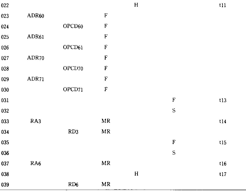
[표 6]TABLE 6

상기 표 6에 나타낸 바와같이 약호로 F,MR,MW만을 나타내고 있다. QSTS4의 란의 H,L은 A프로세서가 QSTS4 단자에 출력한 신호가 하이레벨(H)였는가, 로우레벨(L)였는가를 표시하고 있다. QSTS3-0의 란은 A프로세서가 큐 스테이터스 단자에 출력한 큐 스테이터스의 신호를 제 4 표에 표시한 약호로 F, S, E1만을 표시하고 있다. 우단의 란은, 트레이스 버퍼 메모리의 내용은 아니고, 제 13 도와 표 5와 대응짓기위해 설치한 란으로 t2는 제 13 도중의 t2에 대응하고 있다. 먼저 표 5에 도시한 트레이스 버퍼 메모리의 내용의 덤프 리스트에서 A프로세서가 실제로 실행한 명령을 A프로세서가 실행한 차례로 명령 약호를 얻는 방법을 간단히 설명을 한다.As shown in Table 6, only F, MR, and MW are shown by the symbol. H and L in the column of QSTS4 indicate whether the signal output from the A processor to the QSTS4 terminal was high level (H) or low level (L). The column of QSTS3-0 is the abbreviation of the cue status signal output from the A processor to the cue status terminal in the fourth table, and only F, S, and E 1 are displayed. Is at the right end is the one not the content of the trace buffer memory, installed to build corresponding to the
본 명령 트레이스의 기준으로서, 프로세서의 명령 트레이스법과 같이 큐 스테이터스가, 명령큐의 내용이 모두 파지된 것을 도시하는 시점을 선택한다. 표 5에서는 프레임(021)에 있어서 QSTS3-0이 E1(명령큐의 내용파지)를 표시하고 있으므로, 표 5의 트레시스 버퍼 메모리에서 명령 트레이스를 행하는 기준으로 하여 프레임을 선택한다. 프레임(021)에서 QSTS3-0이 E1을 표시한 후, 최초로 QSTS3-0이 F를 표시하는 것은 프레임(031)이며, 프레임(031)의 다음에 QSTS3-0이 F를 표시하는 것은 프레임(035)이다. 프레임(031)과 프레임(035)사이에서 QST3-0이 S를 표시하는 것은 프레임(032)뿐이므로, 프레임(031)에서 명령코드의 제 1 바이트째가 명령큐에서 인출되어서 명령 해독부로 전송된 명령은 2바이트 길이의 명령코드를 갖는 명령이다. 프레임(031)에서 명령코드의 제 1 바이트째가 명령큐에서 인출된 명령의 가령 명령 I으로 명칭한다. 다음으로 명령 I 의 명령코드를 선출한다. 프레임(021)에서 명령큐의 내용이 모두 파지된 후, 최초의 명령코드 펫치는 프레임(023)과 프레임(024)이다. 프레임(023)에서는 출력한 프리펫치용 어드레스에 대응하는 메모리내의 영역에서 출력된 명령코드는 프레임(024)의 데이타란의 OPCD60이다. 프레임(023) 및 프레임(024)에 의해 명령 I의 제 1 바이트째의 명령코드는 OPCD60인 것을 알 수 있다. 프레임023 및 프레임024의 다음의 명령코드 펫치는 프레임 025 및 프레임 026으로 행해지고 있으며, 명령코드 OPCD61가 A프로세서내에 내장되어 있으므로, 2바이트 길이의 명령코드를 갖는 명령 I의 명령코드는 OPCD60,OPCD61이다. 2바이트 길이의 명령코드 OPCD60,OPCD61을 역 어셈블하면 MOVM60,M61라는 약호가 얻어지므로,명령 I의 명령 약호는 MOVM60,M61이다. 이하 동일한 조작을 반복하면, 프레임(035)에서 명령코드의 제 1 바이트째를 또한 프레임(036)에서 명령코드의 2바이트째를 명령큐에서 인출된 명령은 2바이트 길이의 명령코드를 갖는 명령에서, 명령코드는 명령 I의 프리펫치의 다음 2회의 프리펫치 즉 (027),(028) 및 프레임(029),(030)에서의 명령코드이므로, OPCD70,OPCD71이며, 역 어셈블하면 MOVM70,M71을 얻는다.As a criterion of the instruction trace, the queue status selects a time point at which the contents of the instruction queue are held, as in the instruction trace method of the processor. In Table 5, since QSTS3-0 indicates E 1 (content of the contents of the instruction queue) in the
다음으로 A프로세서가 실행한 명령이 A프로세서 외부의 메모리 또는I/O에 오퍼랜드를 갖는 경우는, 이 오퍼랜드의 실제의 값, 곧 어떤 어드레스에 대해 어떠한 데이타를 엑세스 하였는가를 트레이스 하지 않으면 않된다. 명령 I을 예로 하여 설명을 한다. 명령 I은, 메모리내에 리드 오퍼랜드 M61과, 라이트 오퍼랜드 M60를 필요로 하는 전송명령이다. A프로세서의 리드 오퍼랜드 선독기능에 의해 명령 I의 리드 오퍼랜드가, 명령 I의 명령 해독부에 있어서 명령 해독후 명령 I의 명령 실행부에 있어서 명령 실행 종료전의 사이에 메모리에서 독출된다. 그러나 명령 I의 MOVM60,M61의 리드 오퍼랜드의 어드레스가 간접 어드레싱에 의해 얻어진다면, 명령 I의 리드 오퍼랜드의 어드레스의 값이 명령 I의 명령코드중에는 양으로 나타나지 아니하므로, 표 5의 담프 리스트중의 메모리 리드(BUS-STS가 MR을 표시한다)를 표시하고 있는 몇개의 프레임중의 어느 프레임에서의 메모리 리드가 명령 I의 리드 오퍼랜드의 기억을 위한 메모리 리드를 행하고 있는 프레임인가를 특정지을 수가 없다. 표 5에는, 프레임(003)과 (004)의 메모리 리드, 프레임(010)과 (011)의 메모리 리드, 프레임(033)과 (034)의 메모리 리드, 프레임(037)과 (039)의 메모리 리드의 4개이다. 프레임(003)과 (004)의 메모리 리드와 프레임(010)과 (011)의 메모리 리드는 명령 I의 디코드가 행해지는 프레임(031)보다 시간적으로 앞에 있으므로, 프레임(003)과 (004)의 메모리 리드와, 프레임(010)과 (011)의 메모리 리드는 명령 I의 리드 오퍼랜드를 메모리에서 독출하기 위한 메모리 리드 버스 싸이클은 아닌것은 명백하다. 명령 I의 디코드가 행해지는 프레임(031)보다 시간적으로 뒤에 있는 프레임(033)과 (034)에서의 메모리 리드, 프레임(037)과 (039)에서의 메모리 리드 및 표 5에는 표시되어 있지 않는 프레임(39)이후에 나타나게 될 메모리 리드의 프레임이 명령 I의 리드 오퍼랜드의 메모리로부터의 독출을 위한 메모리 리드 버스 싸이클인 가능성이 있으나, 그중의 어느 프레임이 명령 I의 리드 오퍼랜드를 위한 메모리 리드 버스 싸이클인가를 특정지울 수가 없다. 따라서, 명령 I의 약호를 얻는 일은 가능해도, 명령 I이 어떠한 값의 리드 오퍼랜드를 어떤 어드레스에서 얻었는가를 표시하는 정보가 없기 때문에, 명령 I의 동작의 완전한 복원이 불가능하다.Next, when an instruction executed by A processor has an operand in memory or I / O outside A processor, it must trace the actual value of this operand, which data is accessed for which address. The command I is described as an example. The instruction I is a transfer instruction that requires the read operand M61 and the write operand M60 in the memory. By the read operand read function of the A processor, the read operand of the instruction I is read out from the memory between the instruction decryption portion of the instruction I and the instruction execution portion of the instruction I before the instruction execution completion. However, if the address of the read operands of MOVM60 and M61 of the instruction I is obtained by indirect addressing, the value of the address of the read operand of the instruction I does not appear positive in the instruction code of the instruction I. It is not possible to specify whether the memory read in any of the frames indicating reads (BUS-STS indicates MR) is a frame that is performing a memory read for storing the read operand of the instruction I. Table 5 shows the memory leads of frames 003 and 004, the memory leads of frames 010 and 011, the memory leads of
이상으로 설명을 한 바와같이, 명령코드 프리펫치 기능만을 갖는 정보처리장치에 대해, 명령 실행동작을 이 정보처리장치 외부에 설치한 수단에 의해 추적할 수 가 있도록 정보처리장치에서 내부의 명령코드 프리펫치 큐의 상태를 표시하는 정보와 버스 싸이클의 종류를 도시하는 정보의 이 정보처리장치의 외부로의 출력을 필요 충분하도록 하는 종래의 명령 트레이스 방법은, 다단 파이프 라인 구조를 갖고, 명령코드 프리펫치 기능, 리드 오퍼랜드 선독기능, 라이트 오퍼랜드 뒤에 쓰기 기능을 갖는 고성능의 정보처리장치에 대해서는 하등의 효과가 없는 결점을 갖고 있었다.As described above, for an information processing apparatus having only a command code prefetch function, an internal command code preprocessing is executed in the information processing apparatus so that the command execution operation can be traced by means provided outside the information processing apparatus. The conventional command tracing method of sufficiently outputting information indicating the status of the patch queue and information indicating the type of bus cycle to the outside of this information processing apparatus has a multi-stage pipeline structure, and has a command code prefetching method. The high-performance information processing apparatus having the function, the read operand read function, and the write function after the write operand had no disadvantages.
본 발명은 다단 스테이지의 파이프 라인 구조를 실현하고 있는 마이크로 프로세서에 있어서, 마이크로 프로세서 내부에 소정의 명령의 명령코드가 해독되는 출력이 변환하는 스테이터스 플립플롭과, 이 스테이터스 플립플롭의 출력을 마이크로 프로세서의 버스 싸이클 기간의 어드레스의 출력 타이밍에 동기하여 마이크로 프로세서 외부 출력하는 수단과, 마이크로 프로세서 외부에 마이크로 프로세서의 입출력단자에 나타나는 정보를 차례로 시계열 데이타로서 축적하는 수단을 설치하고, 마이크로 프로세서 내부에 있는 스테이터스 플립플롭에서 마이크로 프로세서 외부로 출력되는 정보를 참조하여, 마이크로 프로세서의 버스 싸이클이 스테이터스 플립플롭의 출력을 변화시키는 소정의 명령에 부수하는 버스 싸이클인가, 혹은 소정의 명령 이후의 명령에 부수하는 버스 싸이클인가를 구별하여 시계열 데이타를 편집하도록 한 것을 특징으로 한다.The present invention provides a microprocessor in which a multi-stage pipeline structure is implemented, comprising: a status flip-flop for converting an output from which an instruction code of a predetermined instruction is decoded into a microprocessor, and outputting the output of the status flip-flop to a microprocessor. A means for externally outputting the microprocessor in synchronization with the output timing of the address of the bus cycle period, and a means for accumulating, as time series data, information displayed on the input / output terminals of the microprocessor in order to the outside of the microprocessor, and a status flip inside the microprocessor. With reference to the information output from the flop to the outside of the microprocessor, the bus cycle of the microprocessor is a bus cycle accompanying a predetermined instruction that changes the output of the status flip-flop, or after the predetermined instruction. Distinguish the bus cycle is incidental to commands is characterized in that one to edit the time-series data.
[실시예]EXAMPLE
제 1 도는 본 발명의 1실시예의 블럭도이다. (101)은 마이크로 프로세서 칩, (102)는 프로세서(102)의 어드레스 버스 신호로, (103)은 프로세서(101)의 데이타 버스 신호로, (104)는 프로세서(101)내의 데이타 버스, (105)는 프로세서(101)의 명령 프리펫치부에서, 명령 프리펫치부(105)내에는 FIFO 구조의 수바이트의 명령코드를 격납하는 명령큐와, 명령큐 제어회로를 갖는다. (106)은 명령 프리펫치부내의 명령큐의 선두에 있는 명령코드를 명령 해독부(107)로 전송하기 위한 신호로, (107)은 명령 해독부에서, 명령 해독부(107)내에는 수바이트의 해독중의 명령코드를 격납하는 명령코드 레지스터와 명령 디코더와 명령 해독부의 동작을 제어하는 시퀀서 등으로 이루어진다. (108)은 명령 해독부에 있어서 디코드된 결과 얻어지는 정보중에서 명령 실행부(110)의 동작을 지정하는 정보를 격납하는 FIFO 구조의 디코드 정보큐, (109)는 디코드 정보큐, (109)는 디코드 정보큐(108)로부터의 정보를 명령 실행부(110)로 전달하기 위한 신호로, (110)은 명령 실행부에서, 산술논리 연산회로, 각종 레지스터등의 하드웨어를 갖는다. (111)은 명령 해독부(107)로부터의 정보 및 지령에 의해 어드레스 계산을 행하는 어드레스 생성부, (112)는 어드레스 생성부(111)에서 생성된 어드레스를 버스 제어부(113)의 어드레스 버스 인터페이스부로 전달하기 위한 신호로이다. (113)은 프로세서(101)의 버스 제어부이다. 버스 제어부(113)은 기능적으로 대별하여 어드레스 버스 인터페이스부, 데이타 버스 인터페이스부, 버스 사이클 제어부의 3개의 부분으로 나누어진다. 어드레스 버스 인터페이스부는 프로세서(101)의 어드레스 버스(102)로부터 프로세서(111)를 포함하는 정보처리시스템 어드레스 버스위에 정해진 어드레스를 출력하는 기능을 가지고, 각종 어드레스를 격납하여 두는 어드레스 레지스터군(119)등의 하드웨어를 갖는다. 데이타 버스 인터페이스부는 프로세서(101)의 데이타 버스(103)를 거쳐서 시스템 데이타 버스와 프로세서(101)의 내부와의 데이타의 수수를 담당하는 부분으로, 데이타 버스(103)를 거쳐 시스템 데이타 버스에서 데이타를 내장하여 일시적으로 축적하여 두는 기억 텝포러리 레지스터(1116), 또한 시스템 데이타 버스위에 데이타를 출력할 때에 데이타 출력에 앞서서 프로세서(101)내에서 생성된 데이타를 일시 축적하여 두는 기록 템포러리 레지스터(117)등의 하드웨어를 갖는다. 버스 제어부(113)내의 버스 사이클 제어부는 프로세서(101)의 버스 사이클 제어, 버스 스테이터스 출력 제어 프로세서(101)의 외부 단자로부터의 신호의 입출력 제어의 기능을 갖는다. (115)는 명령 해독부(107)가 반 제어부(113)에 대해 동작을 지정하는 정보를 공급하여, 또한 버스 제어부(113)가 명령 해독부(107)에 의해 버스 제어부(113)의 내부 상태의 정보를 전달하기 위한 신호로, (114)는 명령 해독부(107)가 어드레스 생성부(111)에 대해 어드레스 생성에 필요한 정보와 어드레스 생성부(111)의 동작을 지정하는 정보를 공급하여, 또한 어드레스 생성부(111)가 명령 해독부(107)에 대해 어드레스 생성부(111)의 내부 상태의 정보를 전달하기 위한 신호로를 정리하여 도시한 것이다. (118)은 명령 실행부(110)내에서 생성한 데이타를 버스 제어부(113)내의 데이타 버스 인터페이스부에 있는 기록 템포러리 레지스터(117)로 전송하여, 또한 버스 제어부(113)내의 데이타 버스 인터페이스부인 기록 템포러리 레지스터(116)에서 명령 실행부(110)로 전송하기 위한 신호로이다, (120)은 프로세서(101)의 버스 스테이터스 신호로, (121)은 메모리 I/O신호(MMIO)나 리드 라이트 신호(RDWR) 등의 프로세서(101)의 외부로 출력하는 신호로를 정리하여 도시한 것이다. (122)는 프로세서(101)의 큐 스테이터스 신호로이다. (123),(124),(125),(126)은 본 발명을 실시하기 위해 새롭게 설치된 하드웨어이다. (123)은 명령 해독부(107)내에 설치된 토글 플립플롭으로 , 명령 해독부에 있어서 분기명령이 해독될때마다 출력이 반전하는 회로이다. (124)는 토글 플립플롭(123)의 출력신호의 신호선, (125)는 버스 제어부(113)내의 어드레스 버스 인터페이스부내의 어드레스 레지스터군의 개개의 레지스터에 1 대 1로 대응하는 레지스터군이다. (126)은, 레지스터군(125)의 출력중에서 선택된 신호를 프로세서(101)외에 출력하는 신호로이다.1 is a block diagram of one embodiment of the present invention.
본 실시예는, 제 8 도에 도시한 A프로세서에, 토글 플립플롭(123),신호로(124), 레지스터군(125), 출력 신호로(126)를 부가한 것으로 되어 있으므로 명령 코드 프리펫치 기능, 리드 오퍼랜드 선독 기능, 라이트 오퍼랜드 뒤에 쓰기 기능을 비롯하여 A프로세서의 전기능이 본 실시예의 프로세서(101)의 기능에 포함되어 있다.In this embodiment, since the toggle flip-
제 2 도는, 프로세서(101)내의 버스 제어부내의 어드레스 버스 인터페이스부의 주요부분을 도시한 도면이다. (201)은 제 1 도의 신호로(112)에 해당하며, 신호로(201)는 도시되지 않은 어드레스 생성부에 있어서 생성된 어드레스를 전송하는 신호로이다. (205),(208),(211),(214)는 어드레스 레지스터군이다. (205)는 프리펫치용 어드레스 레지스터(PAR), (208)은 리드 오퍼랜드용 어드레스 레지스터(RAR1), (211)은 리드 오퍼랜드용 어드레스 레지스터(RAR2), (214)는 라이트 오퍼랜드용 어드레스 레지스터(WAR)이다. (206),(209),(212),(215)는 제 1 도(119)에 대응하고 (205),(209),(212),(215)는 각각 레지스터(205),(208),(211),(214)의 래치신호이다. (207)은 레지스터(205)의 출력신호, (210)은 (208)의 출력 신호로, (213)은 레지스터(211)의 출력신호, (216)은 레지스터(214)의 출력신호이다. (217)은 본 발명에 새롭게 부가된 신호로이며, 제 1 도의 신호로(124)에 대응한다. (219),(221),(223),(225)는 각각 레지스터(219)는 레지스터(205)의 레지스터(221)은 레지스터(208)의, 레지스터(223)은 레지스터(211)의, 레지스터(225)는 레지스터(214)의 각각 확장된 부분으로 생각이 된다. (220)은 레지스터(219)의, (222)는 레지스터(221)의 (224)는 레지스터(223)의, (226)은 레지스터(225)의 출력 신호로이다.FIG. 2 is a diagram showing the main part of the address bus interface section in the bus control section of the
(202)는 멀티플렉서로 레지스터(205)에서 출력되는 어드레스와 레지스터(208)에서 출력되는 어드레스 레지스터(211)에서 출력되는 어드레스와 레지스터(214)에서 출력되는 어드레스의 4개의 어드레스와, 레지스터(219)에서 출력되는 신호와 레지스터(221)에서 출력되는 신호와 레지스터(223)에서 출력되는 신호와 레지스터(225)에서 출력되는 신호의 4개의 신호를 입력으로 하여, 선택신호(204)에서 4개의 어드레스중에서 1개의 어드레스를 선택하여 어드레스 출력신호로(203)로 출력함과 동시에, 선택된 어드레스의 격납되어 있던 레지스터에 대응하는 이 레지스터의 확장부분에서의 출력신호를 (218)로 출력한다. 예를들면 선택신호(204)에 의해 레지스터(208)에서 출력된 어드레스가 선택되었을 때에는 신호로(218)위에는 레지스터(222)의 내용이 선택되어 출력된다. 신호로(204),(206),(209),(212),(215)는 도시하지 않은 명령 해독부에 있어서 생성된 제 1 도의 신호로(115)를 거쳐서 버스 제어부로 이동되어 오는 신호이다. 신호로(203)는 제 1 도의 어드레스 버스(102)에 대응하여 신호로(218)는 제 1 도의 (126)은 대응한다. PAR205만이 어드레스의 자동 갱신기능을 갖는다. 아래의 설명을 위해 PAR205의 확장된 부분에서, 신호로(217)위의 정보를 축적하는 부분(219)을 PAT, RAR1에 대해 (221)을 RAT1,RAR2에 대해 (223)을 RAT2, WAR에 대해 (225)를 WAT라 명명한다.202 denotes a multiplexer, four addresses of an address output from the
제 3 도는 제 13 도에 대응하는 타이밍 챠트를 도식화한 도면이다. 종래 예를 비교하기 쉽도록, 제 3 도의 타이밍 챠트는, 표 3에 도시한 어셈블리 언어의 명령 약호와 명령코드를 갖는 명령을 사용해서 기록한 제 11 도의 프로그램이 어셈블되어 제 12 도에 도시하는 바와 같이 메모리내에 격납되어 있는 것으로 가정하여, 프로세서(101)가 제 12 도중의 메모리 어드레스 ADR(10)의 근처에 있는 일련의 명령을 실행할 때의 프로세서(101)의 내부 및 프로세서(101)의 외부 버스 단자에 표시되는 정보의 시간적 상대관계를 도시하고 있다. 프로세서(101)는 상기 A프로세서의 주요 기능을 포함하고 있으므로, 제 3 도의 명령 해독부, 큐 스테이터스, 명령 실행부의 명령처리의 타이밍 및 RAR1, RAR2, WAR, RDR1, RDR2, WDR의 레지스터의 내용이 변화하는 타이밍, 어드레스 버스, 데이타 버스 위에 나타나는 정보의 변화하는 타이밍 등은 제 13 도에 도시한 각 타이밍과 같다. 여기에서는 본 발명에 의해, 새롭게 부가된 기능의 동작에 대해서 설명을 한다.3 is a diagram illustrating a timing chart corresponding to FIG. 13. For easy comparison of the conventional example, the timing chart of FIG. 3 uses the instructions of the assembly language shown in Table 3, and the programs of FIG. 11 recorded using instructions having instruction codes are assembled as shown in FIG. Assuming that it is stored in the memory, the internal bus terminal of the
제 13 도중, 토글 출력이란 제 1 도중의 명령 해독부(107)내에 본 발명에 의해 새롭게 설치된 토글, 플리플롭(123)의 출력 신호용 신호선(124)위의 신호 레벨을 도시하고 있으며, 명령 I1의 명령 해독부에 있어서 명령 해독이 개시되는 시각 t1에서는 하이레벨(H)에 있는 것을 가정한다.Of
JUMP의 2 바이트의 명령코드가 t9에서 명령 해독부에 있어서 명령해독이 개시되고 t10에서 JUMP가 무조건 분기명령인 것이 판단되면, 이 토글 플립 플롭의 출력이 반전하여 로우레벨(L)로 된다. t10의 후, 빨라도 제 3 도의 t17까지는, 이 토글 플립 플롭의 출력은 모두 로우 레벨에 있다. t6에서 프로세서(101) 외부의 메모리에 리드 오퍼랜드 M31을 필요로 하는 명령 I3이 명령 해독부에 있어서 명령 해독되면, 명령 해독부는 어드레스 생성부에 대해 I3의 리드 오퍼랜드 M31의 어드레스 RA3를 생성하여 버스 제어부로 전송할 것을 지령한다. 동시에 명령 해독부는 버스 제어부에 대해 어드레스 생성부에 전송되는 리드 오퍼랜드 M31의 어드레스 RA3를 어드레스 버스 인터페이스부내의 리드 오퍼랜드용 레지스터 RAR1에 격납할 것을 지령한다. 버스 제어부에 대한 이 지령은, 제 2 도중의 신호로(201)에 어드레스 생성부가 RA3을 출력하고 있는 사이에RAR1(208)의 래치 신호로(206)위에 래치신호를 액티브로 하므로서 이루어진다. 래치 신호로(206)위의 래치 신호가 엑티브로 되면, RAR1내에 신호로(201)위에 RA3이 격납됨과 동시에 RAT1(221)에 (217)위의 t0에 있어서 하이 레벨에 있는 신호가 격납된다. 즉, 제 3 도의 도식적인 타이밍 챠트의 t6에 있어서 신호로(201)위의 정보인 RA3를 샘플링하여 RAR1에 격납함과 동시에, 명령 해독부내에 설치한 토글 플립 플롭(123)의 출력을 샘플링하여 RAT1에 격납한다.When it is determined that instruction decoding is started in the instruction decoding section at t 9 and the JUMP is a branch instruction unconditionally at t 10 , the output of this toggle flip flop is inverted to a low level (L). . After t 10 , at least as early as t 17 in FIG. 3, the output of this toggle flip flop is all at the low level. If the instruction I 3 requiring the read operand M31 in the memory outside the
t10에 있어서 토글 플립 플롭(123)은 무조건 분기명령의 명령코드가 명령 해독부에 있어서 명령해독되므로서 출력을 반전한 후, 명령 해독부에 있어서 명령 해독되므로서 출력을 반전한 후, 명령 해독부에 있어서 t13에서 명령해독이 개시되는 명령 I6도 프로세서(101) 외부에 리드 오퍼랜드 M61을 필요로 하는 명령이며, 상기 I3의 경우와 같이 t13에 있어서, 어드레스 생성부에 있어서 생성되는 I6의 리드 오퍼랜드 M61의 어드레스 RA6를 RAR2에 격납함과 동시에 로우레벨에 있는 상기 토글 플립 플롭(123)의 출력을 샘플링하여 RAT2에 격납한다. t14에 있어서 버스 제어부는 RAR1에 격납되어 있는 I3의 리드 오퍼랜드 M31의 어드레스 RA3을 사용해서 M31의 선독을 위한 메모리 리드 버스 싸이클을 기동한다. 제 2 도에서 t14에 있어서 신호로(204)위의 선택신호에 의해, 멀티플렉서(202)의 2개의 출력신호로의 출력으로서 RAR1에서 출력되어 있는 I3의 리드 오퍼랜드 M31의 어드레스 RA3을 선택하여 어드레스 버스(203)로 출력하고 동시에 RAT1에서 출력되고 있는 라이 레벨에 있는 신호를 선택하여 신호로(218)로 출력한다. 제 1 도에서는, t14에 있어서 어드레스 버스(102)에 RA3이 출력되고, 동시에 신호로(126)에는 RAT1에 격납되어 있다. 하이레벨의 신호가 출력된다. 제 3 도의 t14에 있어서 제 3 도의 어드레스 버스란에 RA3이, 또한 제 1 도의 신호로(126), 제 2 도의 신호로(218)에 대응하는 제 3 도의 AT의 란에 하이레벨(H)의 신호가 출력되어 있다.At t 10 , the toggle flip-
다음으로 t16에 있어서, 버스 제어부는 RAR2에 격납되어 있다. I6의 리드 오퍼랜드 M61의 어드레스 RA6을 사용해서 M61의 선독을 위해 메모리 리드 버스 싸이클을 기동한다. 즉, t16에 있어서 제 1 도의 (102), 제 2 도의 (203), 제 3 도의 어드레스 버스의 란에는 I6의 리드 오퍼랜드 M61의 어드레스 RA6가 출력되고, 동시에 제 1 도의 신호로(6), 제 2 도의 신호로(218), 제 3 도의 AT의 란에는, RAT2에 격납되어 있는 로우 레벨의 신호가 출력되고 있다. 또한, 명령 해독부에 있어서, t10에서 명령 해독된 명령코드가 무조건 분기명령인 것이 판명되면, 명령 프리펫치부의 명령큐에 프리펫치되어 있던 명령코드가 모드 무효로 되고, A프로세서와 같이 프로세서(101)에서도 무조건 분기명령의 명령코드내에 지정되어 있는 분기선 어드레스로부터의 명령코드의 프리펫치가 외부 버스 점유의 최고 우선권을 얻는다.In the following t 16, the bus controller is stored in the RAR2. Using the address RA6 of the read operand M61 of I 6 to and activates the memory read bus cycle for seondok of M61. That is, a first-degree (102), a second degree (203), first the address RA6 are output, and at the same time a first-degree signal of the read operand M61 of In I 6 of the
t10에서 명령 해독부(107)가 어드레스 생성부(111)에 대해, JUMP 명령의 명령코드내에 지정되어 있는 분기선을 도시하는 정보를 신호로(114) 경유로 전달하여, 이 분기선 어드레스 ADR60이 생성하고 버스 제어부로 전송할 것을 지령하고, 버스 제어부(113)에 대해 어드레스 생성부에서 전송되어 오는 이 분기선 어드레서 ADR60을 PAR에 격납하여, PAR의 내용을 사용해서 명령코드의 프리펫치 동작을 개시할 것을 지령한다. 여기에서, 어드레스 생성부(111)에서 버스 제어부(113)에 대해서 전송되는 JUMP 명령에 의한 분기의 분기선 어드레스 ADR60을 PAR205에 격납할 때 동시에 PAR205의 확장부분 PAT219에는, 명령 해독부내의 토글 플립 플롭(123)의 출력신호로(217)위의 신호가 격납된다.At t 10 , the
상술하는 바와 같이 PAR205는 어드레스 자동 갱신 기능을 갖고 t10에 있어서 JUMP 명령에 의한 분기의 분기선 어드레스 ADR60이 격납된 후, 명령코드의 프리펫치를 위한 1회의 메모리 리드 버스 싸이클이 종료할 때마다 PAR205의 내용이 갱신되나, PAT219의 내요은 PAR205의 이 어드레스 자동 갱신 기능과는 관계없이, 다음으로 명령해독부(107)로부터의 지령에 의해 PAR205에 새로운 어드레스가 설정될 때까지 불변한다. 버스 제어부(113)내의 어드레스 버스 인터페이스부의 멀티플렉서(202)가 선택 신호로(204)위에 정보에 의해 프리펫치를 위해 PAR205를 선택하여 PAR의 내용을 어드레스 버스단자(203)로 출력함과 함께, PAR219를 선택하여 PAT의 내용을 신호로(218)위로 출력한다. 제 3 도의 예에서는 t10에 있어서 로우레벨에 있는 신호로(217)위의 신호를 PAT219에 샘플링하고 있기 때문에 t10에서 t13까지 계속되는 분기명령 직후의 명령코드 프리펫치동작에서 신호로(126)에서, 어드레스와 같은 타이밍으로 출력되는 신호AT는 로우레벨(L)에 있다.After PAR205 as described above has an address automatic update function of the branching destination address ADR60 of the branch by the JUMP instruction stored in the t 10, each time a single memory read bus cycle for value-free pipette of the instruction code ends in PAR205 Although the contents are updated, the contents of the PAT219 remain unchanged until a new address is set in the PAR205 by the instruction from the
본 실시예에서는, 무조건 분기명령의 명령코드가 명령 해독부에 있어서 명령 해독되면, 명령 해독부내의 토글 플립플롭(123)의 출력이 변화하나, 여기에서 토글 플립플롭(123)의 출력을 변화시키는 요인으로서 무조건 분기명령을 선택한 이유는, 무조건 분기명령은 통상의 프로그램에서는 통계적으로 약 10스텝으로 1회는 사용이 되고 있기 때문이다. 즉, 간혹 사용되는 명령을 토글 플립 플롭(123)의 출력을 변화시키는 요인으로서 사용하면, 명령 트레이스 장치의 유한한 트레이스 버퍼 메모리내에서 한번에 AT가 변화하지 않는 일이 생기면, 본 명령 트레이스가 불가능하게 된다. 따라서, 수 내지 수 10스텝 1회 나탄나는 명령, 혹은, 그 스텝 싸이클로 강제적으로 삽입되는 명령을 사용하는 폭이 좋다.In this embodiment, when the instruction code of the branch instruction unconditionally is decoded in the instruction deciphering unit, the output of the toggle flip-
이상 고도의 파이프 라인구조를 실현하고 있는 A프로세서에 본 발명에 의해 새롭게 부가된 하드웨어의 동작에 대해서 설명하였다. 다음에 본 발명을 실시하고 있는 프로세서(101)를 사용해서 소프트웨어를 개발할때에 사용하는 명령 트레이스법에 대해서 설명한다. 본 발명의 본 명령 트레이스법은, 상술한 A프로세서의 경우의 명령 트레이스법에, 본 발명에 의해 새롭게 부가된 하드웨어에서 얻어지는 정보를 추가하므로서, 상술하는 A프로세서의 경우의 명령 트레이스법의 갖고 있던 중대한 문제점을 근본적으로 해결할 수가 있다.The operation of the hardware newly added by the present invention to the A processor that realizes the high pipeline structure has been described above. Next, an instruction trace method used when developing software using the
본 발명의 명령 트레이스법에 의한 명령 트레이스를 행하기 위한 명령 트레이스 장치에는, 상술하는 A프로세서의 명령 트레이스 장치와 같이, 프로세서(101)가 일련의 명령을 실행하고 있는 동안에 어드레스 버스위의 정보, 필요한 제어신호, 스테이터스 신호 및 상기 신호로(126)에서 출력되는 신호를 샘플링하여 차례로 시계열 데이타로서 축적하는 트레이스 버퍼 메모리 브레이크 포인트 설정기능, 트레이스 버퍼 메모리 내의 시계열 정보의 편집기능 등이 필요하다. 본 발명의 명령 트레이스법이 명령 트레이스의 기준으로서 트레이스 버퍼 메모리내에서 큐 스테이터스가 명령큐의 내용이 모두 무효로 된 것을 도시하는 시점을 사용하고 있는 것 및 본 명령 트레이스법의 이 기준점에서 트레이스 버퍼 메모리내의 시계열 데이타를 추적하여 이 기준점의 직후에 실행된 1명령 몫의 명령코드를 선출하여 역 어셈블하여 이 기준점 직후에 실행된 명령의 약호를 얻는 방법은, 상술한 A프로세서에 대한 명령 트레이스법과 동일하다. 여기에서는 본 발명의 명령 트레이스법에 의해 가능케된, 메모리나 I/O엑세스를 수반하는 명령에 대해서 상기한 역 어셈블에 의해 얻어진 명령 약호와, 이 명령이 실제로 엑세스한 어드레스와 데이타를 명령약호와 대응시키는 방법을 설명한다.The instruction trace apparatus for performing the instruction trace by the instruction trace method of the present invention, like the instruction trace apparatus of the A-processor described above, requires information on the address bus while the
제 11 도에 도시한 프로그램이 어셈블되어서 제 12 도에 도시하는 바와 같이 메모리내에 격납되어 있는 것으로 하여, A프로세서가 제 12 도중의 메모리 어드레스 ADR10의 근처로부터의 일련의 명령을 실행한 때에 프로세서(101)용의 명령 트레이스 장치를 사용해서 명령 트레이스를 행하는 법을 설명한다. 표 7은 프로세서(101)용의 명령 트레이스 장치의 트레이스 버퍼 메모리의 내용의 일부의 담프 리스트이며, 표 5와 대부분이 일치하고 있다. 어드레스를 출력하는 것과 동시에 신호로(126)로 출력하는 신호가 하이레벨(H)이 있거나 로우레벨(L)에 있었던가를 표시하고 있다.When the program shown in Fig. 11 is assembled and stored in the memory as shown in Fig. 12, the
표 7 에 있어서, 프레임(021)에서 QSTS3-0가 E1을 표시하는 점을 기준으로 하면, 표 5에서 사용한 방법에 의해 프레임 031, 032에서 명령 해독부에 있어서 명령 해독되는 2바이트 길이의 명령 코드를 갖는 명령 J의 명령코드는 프레임 023, 024 및 프레임 025, 026에서 프리펫치된 2바이트의 명령코드 OPCD60,OPCD61이며, 명령코드 OPCD60, OPCD61을 역 어셈블하여 명령 J의 명령 약호로서 MOV R6, M61을 얻는다.In Table 7, based on the point where QSTS3-0 indicates E 1 in
[표 7a]TABLE 7a

[표 7b]TABLE 7b

명령 J는, 메모리내에 리드 오퍼랜드 M61를 필요로 하는 전송명령이므로, 명령 J의 명령 트레이스를 위해서는 명령 J의 리드 오퍼랜드 M61로서 어떠한 메모리 어드레스로부터, 어떠한 데이타가 프로세서(101)내에 내장되었는가를 표시하지 않으면 안된다. 이로 인하여, 표 7에 새롭게 가해진 AT의 란의 정보를 사용한다.Since the instruction J is a transfer instruction requiring a read operand M61 in the memory, if the instruction trace of the instruction J does not indicate which memory address is embedded in the
AT의 란의 정보는, 프로세서(101)의 어드레스 단자(102)로 출력되는 어드레스가 버스 제어부 내의 어드레스 레지스터에 격납될때의, 명령 해독부 내의 토글 플립플롭(123)의 출력의 상태를 기억하고 있는 것이다. 이 토글 플립플롭(123)은 명령 해독부에서 무조건 분기명령의 명령코드를 해독된 순간에 출력을 반전한다. 무조건 분기명령의 해독은, 큐 스테이터스 QSTS 3-0이 E1을 표시하는 것으로 프로세서(101)외부에 즉시로 표시되기 때문에, QSTS 3-0이 E1을 도시하는 프레임 021의 전후의 프리펫치를 위한 어드레스 출력시의 AT의 값을 보면, 프레임(021)전에는 AT는 하이 레벨(H)에 있으며, 프레임(021)의 뒤에서는 AT가 로우 레벨(L)로 되어 있음을 판단할 수 있다. 무조건 분기명령 해독 직후에 있는 전송명령 J의 명령코드가 프레임(021)보다도 뒤에 명령 해독부에 있어서 명령 해독되어, 이 명령 J의 리드 오퍼랜드 M61의 어드레스가 어드레스 생성부에서 생성되고 버스 제어부의 어드레스 레지스터군에 격납될때에 이 어드레스 레지스터의 확장부분에는, 로우 레벨에 있는 토글 플립플롭(123)의 출력이 격납된다. 따라서 메모리내에 리드 오퍼랜드 M61를 필요로 하는 명령 J의 리드 오퍼랜드의 기록을 위한 메모리 리드 버스 싸이클은, 프레임(021)보다 뒤의 프레임중에서, 처음으로 AT가 L(로우 레벨)을 표시하고 있는, 명령코드 프리펫치 이외의 메모리 리드 버스 싸이클이다. 표 8에서는 프레임(021)보다 뒤에 프레임(033),(034)과 프레임(037),(039)의 2회의 메모리 리드 싸이클에 있으나, AT의 란이 프레임(021)보다도 뒤에 처음으로 L를 표시하는 것은 프레임(037)에서의 어드레스 출력이므로, 메모리내에 리드 오퍼랜드 M61를 필요로 하는 명령 J의 리드 오퍼랜드 독입을 위한 버스 싸이클은 프레임(037),(039)에 있어서 메모리 리드 버스 싸이클이며, 명령 J의 리드 오퍼랜드 M61의 어드레스는 프레임(037)에서 RA6이며, M61의 데이타는 프레임(039)의 RD6에인 것이 결정된다. 다음에 동일하게 하여, 무조건 분기명령의 명령코드의 명령 해독후 처음으로 나타나는 메모리내에 리드 오퍼랜드를 필요로 하는 명령 J의 다음에 나타나는 메모리내에 리드 오퍼랜드를 필요로하는 명령의 리드 오퍼랜드 기입을 위한 메모리 리드 버스 싸이클은, 프레임(037),(039)의 다음에 AT가 L을 표시하는 메모리 리드 버스 싸이클인 것이 결정된다. 여기까지의 설명은, 명령 메모리내에 리드 오퍼랜드를 갖는 경우에 대해서 행하여 왔으나, 이 명령 트레이스법의 명령과 오퍼랜드의 대응을 짓는 법은, 오퍼랜드가 메모리내에 있어도 I/O내에 있어서도 완전히 동일하게 행할 수가 있다.The information in the AT field stores the state of the output of the toggle flip-
이상으로 설명을 한 바와같이, 본 발명은 다단 스테이지의 파이프 라인구조를 실현하고 있는 고기능 프로세서내에서, 각 스테이지의 명령처리의 시퀀스를 정하는 명령 해독부내에, 미리 정해진 종류의 명령의 명령코드가 명령해독되면 출력이 반전하는 토글 플립플롭을 설치해, 이 프로세서내의 어드레스 생성부에 있어서 생성된 어드레스가 버스 제어부내의 어드레스 레지스터중의 1개의 격납될때 동시에 이 어드레스 레지스터의 확장부분에 상기 토글 플립플롭의 상태를 격납하여, 버스 제어부가 버스 싸이클을 기동할때에 선택이 되는 어드레스 레지스터의 어드레스 부분을 이 프로세서의 어드레스 버스단자에, 어드레스 레지스터 확장부분의 정보를 이 프로세서의 정보 출력용 단자로 출력하여, 이 프로세서용 명령 트레이스 장치에 있어서 정보 출력용 단자에 나타나는 신호를 이 프로세서의 어드레스 버스 위에 나타나는 신호와 함께 명령 트레이스 장치의 트레이스 버퍼내에 차례로 내장하여, 리드 오퍼랜드 선독 및 라이트 오퍼랜드 뒤에 산기를 하는 프로세서의 명령 트레이스시, 명령약호와 이 명령의 프로세서 외부의 오퍼랜드 엑세스를, 어드레스 레지스터의 확장부분에서 프로세서 외에 어드레스와 함께 출력되는 정보를 기준으로 하여 대응짓는 명령 트레이스법이다.As described above, in the present invention, in a high-performance processor that realizes a multi-stage pipeline structure, an instruction code of a predetermined type of instruction is stored in an instruction decoding unit that determines a sequence of instruction processing for each stage. A toggle flip-flop in which the output is inverted when decrypted is provided, and when the address generated by the address generator in this processor is stored in one of the address registers in the bus control unit, the toggle flip-flop is displayed in an extended portion of the address register. To store the address portion of the address register, which is selected when the bus control section starts the bus cycle, to the address bus terminal of this processor, and to output information of the address register extension portion to the information output terminal of the processor. Information about the command trace device The signal appearing on the output terminal is sequentially embedded in the trace buffer of the instruction trace device along with the signal appearing on the address bus of this processor, so that the instruction abbreviation and instruction abbreviation can be used during the instruction trace of the processor which reads the read operand and writes the operand after the write operand. External operand access is an instruction tracing method that associates an external operand access based on information output with an address other than a processor in an extended portion of the address register.
표 7에 있어서, 어드레스란의 RA1, ADR41…은 프로세서(101)이 어드레스 버스 위에 출력한 어드레스, 데이타란의 RD1,OPCD41…은 프로세서(101)의 데이타 입출력에 의해 데이타 버스위에 나타난 데이타이다. BUS-STS의 란은 프로세서(101)가 버스 스테이터스 단자(120)로 출력한 버스 스테이터스 코드 및 신호로(121)위에 출력되는 MMIO신호, RDWR신호를 표 6에 표시한 약호로 F,MR,MW만을 표시하고 있다. QSTS란의 H,L은 프로세서(101)가 QSTS4단자(122)로 출력한 신호가 하이 레벨(H)에 있었는가 로우 레벨(L)에 있었는가를 표시하고 있다. QSTS 3-0란은 프로세서(101)가 큐 스테이터스 단자(122)로 출력한 큐 스테이터스 신호를 표 4에 표시한 약호로 F,S,E1만을 표시하고 있다. AT의 란은 프로세서(101)가 어드레스 버스단자(102)위에 어드레스를 출력하는 것과 동시에 신호로(126)로 출력하는 신호가 하이 레벨(H)였는가 로우레벨(L)였는가를 표시하고 있다.In Table 7, RA1, ADR41,. Is an address output from the
이 결과, 다단 스테이지의 파이프 라인구조를 실현하고 있는 프로세서가, 이 프로세서의 외부에 오퍼랜드를 필요로 하는 명령의 리드 오퍼랜드의 선독 또는 라이트 오퍼랜드의 뒤에 쓰기를 행하고 있는 경우라도, 이 프로세서가 실행한 명령에 대해서 그 실행순으로 명령약호를 얻어, 프로세서의 외부에 오퍼랜드를 필요로 하는 명령의 경우에는, 그 명령의 약호와 오퍼랜드가 실제로 엑세스된때의 어드레스와 데이타를 대응지을 수가 있다.As a result, even if the processor implementing the multi-stage pipeline structure writes after the read operand or the write operand of the instruction that requires the operand outside of the processor, the processor executes the instruction. The instruction abbreviation is obtained in order of execution, and in the case of an instruction requiring an operand outside the processor, the instruction abbreviation can be matched with the address and data when the operand is actually accessed.
또한, 표 1은 8086프로세서의 큐 스테이터스의 표, 표 2는 8086프로세서의 버스 스테이터스의 표, 표 3은 A프로세서 및 프로세서(101)의 어셈블리 언어로 쓰여진 프로그램의 명령약호와 명령코드의 대응표, 표 4는 A프로세서 및 프로세서(101)의 큐 스테이터스의 표, 표 5는 A프로세서가, 제 12 도에 도시한 메모리내의 ADR10의 근처에서 차례로 명령을 실행한 때의 명령 트레이스 장치의 트레이스 버퍼 메모리에 축적된 정보의 담프 리스트, 표 6은 Az프로세서 및 프로세서(101)의 버스 스테이터스의 표, 표 7은 프로세서(101)가 제 12 도에 도시한 메모리내의 ADR10의 근처에서 명령을 실행한 때에 명령 트레이스 장치의 트레이스 버퍼 메모리에 축적된 정보의 담프 리스트, 표 6은 A프로세서 및 프로세서(101)의 버스 스테이터스의 표, 표 7은 프로세서(101)가 제 12 도에 도시한 메모리내의 ADR10의 근처에서 차례로 명령을 실행한 때에 명령 트레이스 장치의 트레이스 버퍼 메모리에 축적된 정보의 담프 리스트이다.In addition, Table 1 is a table of the queue status of the 8086 processor, Table 2 is a table of the bus status of the 8086 processor, Table 3 is a table corresponding to the instruction abbreviations and instructions of the program written in the assembly language of the A processor and
본 발명에 의하면, 다단 스테이지의 파이프 라인 기능을 갖는 프로세서로서, 프로세서 외부의 오퍼랜드에 대해 리드 오퍼랜드의 선독 및 라이트 오퍼랜드의 뒤에 쓰기를 하는 프로세서에 있어서, 이 프로세서의 완전한 명령 트레이스가 가능하게 되므로, 프로세서의 소프트웨어 개발과 디백크 효율이 비약적으로 향상하는 효과가 있다.According to the present invention, a processor having a pipeline stage function of a multi-stage stage, in which a processor reads a read operand and writes a write operand to an operand outside the processor, a complete instruction trace of the processor is possible. Software development and de-backpacking efficiency is greatly improved.
Claims (8)
Applications Claiming Priority (2)
| Application Number | Priority Date | Filing Date | Title |
|---|---|---|---|
| JP90702 | 1986-04-18 | ||
| JP61090702A JPH0731615B2 (en) | 1986-04-18 | 1986-04-18 | Information processing equipment |
Publications (2)
| Publication Number | Publication Date |
|---|---|
| KR870010438A KR870010438A (en) | 1987-11-30 |
| KR930008686B1 true KR930008686B1 (en) | 1993-09-11 |
Family
ID=14005856
Family Applications (1)
| Application Number | Title | Priority Date | Filing Date |
|---|---|---|---|
| KR1019870003729A KR930008686B1 (en) | 1986-04-18 | 1987-04-18 | Data processor |
Country Status (5)
| Country | Link |
|---|---|
| US (1) | US4879646A (en) |
| EP (1) | EP0241946B1 (en) |
| JP (1) | JPH0731615B2 (en) |
| KR (1) | KR930008686B1 (en) |
| DE (1) | DE3751356T2 (en) |
Families Citing this family (66)
| Publication number | Priority date | Publication date | Assignee | Title |
|---|---|---|---|---|
| JPH0782448B2 (en) * | 1987-12-10 | 1995-09-06 | 三菱電機株式会社 | Microprocessor |
| JP2982875B2 (en) * | 1987-12-28 | 1999-11-29 | 株式会社日立製作所 | Slave controller |
| JP2678283B2 (en) * | 1988-03-15 | 1997-11-17 | 株式会社日立製作所 | Data communication controller |
| JPH0233631A (en) * | 1988-07-22 | 1990-02-02 | Fujitsu Ltd | Advance control tracing system |
| JPH02133834A (en) * | 1988-11-14 | 1990-05-23 | Nec Corp | In-circuit emulator |
| CA2016068C (en) * | 1989-05-24 | 2000-04-04 | Robert W. Horst | Multiple instruction issue computer architecture |
| JPH06105432B2 (en) * | 1989-06-01 | 1994-12-21 | 三菱電機株式会社 | Microprocessor |
| FR2649507B1 (en) * | 1989-07-07 | 1994-07-08 | Bull Sa | METHOD FOR OBSERVING THE EXECUTION OF A PROGRAM LOADED IN A COMPUTER SYSTEM AND DEVICE FOR CARRYING OUT SAID METHOD |
| US5412799A (en) * | 1990-02-27 | 1995-05-02 | Massachusetts Institute Of Technology | Efficient data processor instrumentation for systematic program debugging and development |
| JPH0511827A (en) * | 1990-04-23 | 1993-01-22 | Canon Inc | Execution time output system of industrial automatic device |
| US5151981A (en) * | 1990-07-13 | 1992-09-29 | International Business Machines Corporation | Instruction sampling instrumentation |
| JP2505950B2 (en) * | 1991-05-13 | 1996-06-12 | インターナショナル・ビジネス・マシーンズ・コーポレイション | Hardware support break point system |
| US5625821A (en) * | 1991-08-12 | 1997-04-29 | International Business Machines Corporation | Asynchronous or synchronous operation of event signaller by event management services in a computer system |
| US5355484A (en) * | 1991-08-12 | 1994-10-11 | International Business Machines Corporation | Dynamically established event monitors in event management services of a computer system |
| US5237684A (en) * | 1991-08-12 | 1993-08-17 | International Business Machines Corporation | Customized and versatile event monitor within event management services of a computer system |
| US5305454A (en) * | 1991-08-12 | 1994-04-19 | International Business Machines Corporation | Notification of event handlers in broadcast or propagation mode by event management services in a computer system |
| US5345569A (en) * | 1991-09-20 | 1994-09-06 | Advanced Micro Devices, Inc. | Apparatus and method for resolving dependencies among a plurality of instructions within a storage device |
| JP2693678B2 (en) * | 1992-01-28 | 1997-12-24 | 株式会社東芝 | Data processing device |
| JP3544214B2 (en) * | 1992-04-29 | 2004-07-21 | サン・マイクロシステムズ・インコーポレイテッド | Method and system for monitoring processor status |
| US5367657A (en) * | 1992-10-01 | 1994-11-22 | Intel Corporation | Method and apparatus for efficient read prefetching of instruction code data in computer memory subsystems |
| US5383192A (en) * | 1992-12-23 | 1995-01-17 | Intel Corporation | Minimizing the likelihood of slip between the instant a candidate for a break event is generated and the instant a microprocessor is instructed to perform a break, without missing breakpoints |
| US5410686A (en) * | 1993-11-01 | 1995-04-25 | Motorola, Inc. | Methods for scan path debugging |
| JPH07182182A (en) * | 1993-12-21 | 1995-07-21 | Mitsubishi Electric Corp | Collecting device for system information |
| US5922070A (en) * | 1994-01-11 | 1999-07-13 | Texas Instruments Incorporated | Pipelined data processing including program counter recycling |
| US5724566A (en) * | 1994-01-11 | 1998-03-03 | Texas Instruments Incorporated | Pipelined data processing including interrupts |
| US5680583A (en) * | 1994-02-16 | 1997-10-21 | Arkos Design, Inc. | Method and apparatus for a trace buffer in an emulation system |
| US5446876A (en) * | 1994-04-15 | 1995-08-29 | International Business Machines Corporation | Hardware mechanism for instruction/data address tracing |
| US5920712A (en) * | 1994-05-13 | 1999-07-06 | Quickturn Design Systems, Inc. | Emulation system having multiple emulator clock cycles per emulated clock cycle |
| US5850562A (en) * | 1994-06-27 | 1998-12-15 | International Business Machines Corporation | Personal computer apparatus and method for monitoring memory locations states for facilitating debugging of post and BIOS code |
| US5642478A (en) * | 1994-12-29 | 1997-06-24 | International Business Machines Corporation | Distributed trace data acquisition system |
| US5819065A (en) * | 1995-06-28 | 1998-10-06 | Quickturn Design Systems, Inc. | System and method for emulating memory |
| US5923865A (en) * | 1995-06-28 | 1999-07-13 | Quickturn Design Systems, Inc. | Emulation system having multiple emulated clock cycles per emulator clock cycle and improved signal routing |
| US5754827A (en) * | 1995-10-13 | 1998-05-19 | Mentor Graphics Corporation | Method and apparatus for performing fully visible tracing of an emulation |
| US5678003A (en) * | 1995-10-20 | 1997-10-14 | International Business Machines Corporation | Method and system for providing a restartable stop in a multiprocessor system |
| US5822564A (en) * | 1996-06-03 | 1998-10-13 | Quickturn Design Systems, Inc. | Checkpointing in an emulation system |
| US6003107A (en) * | 1996-09-10 | 1999-12-14 | Hewlett-Packard Company | Circuitry for providing external access to signals that are internal to an integrated circuit chip package |
| US5881224A (en) * | 1996-09-10 | 1999-03-09 | Hewlett-Packard Company | Apparatus and method for tracking events in a microprocessor that can retire more than one instruction during a clock cycle |
| US5887003A (en) * | 1996-09-10 | 1999-03-23 | Hewlett-Packard Company | Apparatus and method for comparing a group of binary fields with an expected pattern to generate match results |
| US5867644A (en) * | 1996-09-10 | 1999-02-02 | Hewlett Packard Company | System and method for on-chip debug support and performance monitoring in a microprocessor |
| US5956476A (en) * | 1996-10-31 | 1999-09-21 | Hewlett Packard Company | Circuitry and method for detecting signal patterns on a bus using dynamically changing expected patterns |
| US5956477A (en) * | 1996-11-25 | 1999-09-21 | Hewlett-Packard Company | Method for processing information in a microprocessor to facilitate debug and performance monitoring |
| US6009539A (en) * | 1996-11-27 | 1999-12-28 | Hewlett-Packard Company | Cross-triggering CPUs for enhanced test operations in a multi-CPU computer system |
| US5881217A (en) * | 1996-11-27 | 1999-03-09 | Hewlett-Packard Company | Input comparison circuitry and method for a programmable state machine |
| US5960191A (en) * | 1997-05-30 | 1999-09-28 | Quickturn Design Systems, Inc. | Emulation system with time-multiplexed interconnect |
| US5970240A (en) * | 1997-06-25 | 1999-10-19 | Quickturn Design Systems, Inc. | Method and apparatus for configurable memory emulation |
| US6202199B1 (en) * | 1997-07-31 | 2001-03-13 | Mutek Solutions, Ltd. | System and method for remotely analyzing the execution of computer programs |
| JP3214613B2 (en) * | 1998-07-03 | 2001-10-02 | 日本電気株式会社 | Microprocessor and data processing system |
| US6374370B1 (en) | 1998-10-30 | 2002-04-16 | Hewlett-Packard Company | Method and system for flexible control of BIST registers based upon on-chip events |
| US6393606B1 (en) * | 1999-06-25 | 2002-05-21 | Agilent Technologies, Inc. | Inverse assembler |
| US6446029B1 (en) * | 1999-06-30 | 2002-09-03 | International Business Machines Corporation | Method and system for providing temporal threshold support during performance monitoring of a pipelined processor |
| US20020087949A1 (en) * | 2000-03-03 | 2002-07-04 | Valery Golender | System and method for software diagnostics using a combination of visual and dynamic tracing |
| US8312435B2 (en) | 2000-12-26 | 2012-11-13 | Identify Software Ltd. (IL) | System and method for conditional tracing of computer programs |
| US7069545B2 (en) * | 2000-12-29 | 2006-06-27 | Intel Corporation | Quantization and compression for computation reuse |
| US7386839B1 (en) | 2002-11-06 | 2008-06-10 | Valery Golender | System and method for troubleshooting software configuration problems using application tracing |
| US8032866B1 (en) | 2003-03-27 | 2011-10-04 | Identify Software Ltd. | System and method for troubleshooting runtime software problems using application learning |
| US7328429B2 (en) * | 2003-11-13 | 2008-02-05 | Intel Corporation | Instruction operand tracing for software debug |
| US7827539B1 (en) | 2004-06-25 | 2010-11-02 | Identify Software Ltd. | System and method for automated tuning of program execution tracing |
| US20090178032A1 (en) * | 2005-03-03 | 2009-07-09 | Rongzhen Yang | Mining for performance data for systems with dynamic compilers |
| US8108198B2 (en) * | 2006-02-21 | 2012-01-31 | Mentor Graphics Corporation | Memory tracing in an emulation environment |
| US8010774B2 (en) * | 2006-03-13 | 2011-08-30 | Arm Limited | Breakpointing on register access events or I/O port access events |
| US20070226471A1 (en) * | 2006-03-13 | 2007-09-27 | Arm Limited | Data processing apparatus |
| US7555424B2 (en) | 2006-03-16 | 2009-06-30 | Quickturn Design Systems, Inc. | Method and apparatus for rewinding emulated memory circuits |
| JP2008071227A (en) * | 2006-09-15 | 2008-03-27 | Nec Electronics Corp | Semiconductor integrated circuit |
| US9811335B1 (en) * | 2013-10-14 | 2017-11-07 | Quicklogic Corporation | Assigning operational codes to lists of values of control signals selected from a processor design based on end-user software |
| US9760494B2 (en) | 2015-06-24 | 2017-09-12 | International Business Machines Corporation | Hybrid tracking of transaction read and write sets |
| US9858189B2 (en) | 2015-06-24 | 2018-01-02 | International Business Machines Corporation | Hybrid tracking of transaction read and write sets |
Family Cites Families (9)
| Publication number | Priority date | Publication date | Assignee | Title |
|---|---|---|---|---|
| JPS6042968B2 (en) * | 1978-02-07 | 1985-09-26 | 日本電気株式会社 | information processing equipment |
| JPS5916370B2 (en) * | 1979-05-07 | 1984-04-14 | 株式会社明電舎 | Vacuum cutter |
| JPS56140931A (en) * | 1980-04-04 | 1981-11-04 | Nippon Zeon Co Ltd | Preparation of conjugated diolefin |
| JPS56140932A (en) * | 1980-04-07 | 1981-11-04 | Toray Ind Inc | Isolation of cyclohexene by adsorption |
| US4390946A (en) * | 1980-10-20 | 1983-06-28 | Control Data Corporation | Lookahead addressing in a pipeline computer control store with separate memory segments for single and multiple microcode instruction sequences |
| US4430706A (en) * | 1980-10-27 | 1984-02-07 | Burroughs Corporation | Branch prediction apparatus and method for a data processing system |
| US4477872A (en) * | 1982-01-15 | 1984-10-16 | International Business Machines Corporation | Decode history table for conditional branch instructions |
| JPS58181152A (en) * | 1982-04-15 | 1983-10-22 | Fujitsu Ltd | Debugging system of data processing device |
| US4775927A (en) * | 1984-10-31 | 1988-10-04 | International Business Machines Corporation | Processor including fetch operation for branch instruction with control tag |
-
1986
- 1986-04-18 JP JP61090702A patent/JPH0731615B2/en not_active Expired - Fee Related
-
1987
- 1987-04-18 KR KR1019870003729A patent/KR930008686B1/en not_active IP Right Cessation
- 1987-04-20 US US07/039,900 patent/US4879646A/en not_active Expired - Lifetime
- 1987-04-21 DE DE3751356T patent/DE3751356T2/en not_active Expired - Fee Related
- 1987-04-21 EP EP87105823A patent/EP0241946B1/en not_active Expired - Lifetime
Also Published As
| Publication number | Publication date |
|---|---|
| JPH0731615B2 (en) | 1995-04-10 |
| US4879646A (en) | 1989-11-07 |
| EP0241946B1 (en) | 1995-06-21 |
| EP0241946A3 (en) | 1989-12-27 |
| JPS62245442A (en) | 1987-10-26 |
| KR870010438A (en) | 1987-11-30 |
| DE3751356T2 (en) | 1995-12-14 |
| EP0241946A2 (en) | 1987-10-21 |
| DE3751356D1 (en) | 1995-07-27 |
Similar Documents
| Publication | Publication Date | Title |
|---|---|---|
| KR930008686B1 (en) | Data processor | |
| US7197671B2 (en) | Generation of trace elements within a data processing apparatus | |
| US7533302B2 (en) | Trace and debug method and system for a processor | |
| US5446849A (en) | Electronic computer which executes squash branching | |
| KR920006275B1 (en) | Data processing apparatus | |
| JP2693678B2 (en) | Data processing device | |
| JP2003085000A (en) | Trace information production device and its method | |
| KR19980063936A (en) | Information processing unit with high hit rate branch prediction with small hardware | |
| JP2001525568A (en) | Instruction decoder | |
| JP2734468B2 (en) | Processor | |
| JPH1196004A (en) | Method and device for controlling condition branch execution by data processor | |
| JP2001051874A (en) | Microcomputer | |
| JPH03233630A (en) | Information processor | |
| JPH0743648B2 (en) | Information processing equipment | |
| EP0279953A2 (en) | Computer system having mixed macrocode and microcode instruction execution | |
| US5421026A (en) | Data processor for processing instruction after conditional branch instruction at high speed | |
| EP0374598A2 (en) | Control store addressing from multiple sources | |
| US5787276A (en) | Microprocessor including circuit for generating signal used for tracing executed instruction stream | |
| JP2758624B2 (en) | Speed control method of micro program | |
| KR920001102B1 (en) | Data processing unit | |
| JPH087713B2 (en) | Microprocessor | |
| JPH0752402B2 (en) | Data processing device | |
| JPH1011290A (en) | Microprocessor | |
| JPH0784827A (en) | Trace device | |
| WO1986000435A1 (en) | Three word instruction pipeline |
Legal Events
| Date | Code | Title | Description |
|---|---|---|---|
| A201 | Request for examination | ||
| G160 | Decision to publish patent application | ||
| E701 | Decision to grant or registration of patent right | ||
| GRNT | Written decision to grant | ||
| FPAY | Annual fee payment |
Payment date: 20040910 Year of fee payment: 12 |
|
| LAPS | Lapse due to unpaid annual fee |