KR910007835B1 - Primary particle beam irradiation apparatus and method of irradiation thereof - Google Patents
Primary particle beam irradiation apparatus and method of irradiation thereof Download PDFInfo
- Publication number
- KR910007835B1 KR910007835B1 KR1019870010878A KR870010878A KR910007835B1 KR 910007835 B1 KR910007835 B1 KR 910007835B1 KR 1019870010878 A KR1019870010878 A KR 1019870010878A KR 870010878 A KR870010878 A KR 870010878A KR 910007835 B1 KR910007835 B1 KR 910007835B1
- Authority
- KR
- South Korea
- Prior art keywords
- primary particle
- particle beam
- irradiation
- secondary ion
- ion sensor
- Prior art date
Links
Images


Classifications
-
- H—ELECTRICITY
- H01—ELECTRIC ELEMENTS
- H01L—SEMICONDUCTOR DEVICES NOT COVERED BY CLASS H10
- H01L21/00—Processes or apparatus adapted for the manufacture or treatment of semiconductor or solid state devices or of parts thereof
- H01L21/02—Manufacture or treatment of semiconductor devices or of parts thereof
- H01L21/04—Manufacture or treatment of semiconductor devices or of parts thereof the devices having at least one potential-jump barrier or surface barrier, e.g. PN junction, depletion layer or carrier concentration layer
- H01L21/18—Manufacture or treatment of semiconductor devices or of parts thereof the devices having at least one potential-jump barrier or surface barrier, e.g. PN junction, depletion layer or carrier concentration layer the devices having semiconductor bodies comprising elements of Group IV of the Periodic System or AIIIBV compounds with or without impurities, e.g. doping materials
- H01L21/26—Bombardment with radiation
- H01L21/263—Bombardment with radiation with high-energy radiation
- H01L21/265—Bombardment with radiation with high-energy radiation producing ion implantation
-
- H—ELECTRICITY
- H01—ELECTRIC ELEMENTS
- H01J—ELECTRIC DISCHARGE TUBES OR DISCHARGE LAMPS
- H01J37/00—Discharge tubes with provision for introducing objects or material to be exposed to the discharge, e.g. for the purpose of examination or processing thereof
- H01J37/30—Electron-beam or ion-beam tubes for localised treatment of objects
- H01J37/317—Electron-beam or ion-beam tubes for localised treatment of objects for changing properties of the objects or for applying thin layers thereon, e.g. for ion implantation
- H01J37/3171—Electron-beam or ion-beam tubes for localised treatment of objects for changing properties of the objects or for applying thin layers thereon, e.g. for ion implantation for ion implantation
-
- H—ELECTRICITY
- H01—ELECTRIC ELEMENTS
- H01J—ELECTRIC DISCHARGE TUBES OR DISCHARGE LAMPS
- H01J37/00—Discharge tubes with provision for introducing objects or material to be exposed to the discharge, e.g. for the purpose of examination or processing thereof
- H01J37/30—Electron-beam or ion-beam tubes for localised treatment of objects
- H01J37/304—Controlling tubes by information coming from the objects or from the beam, e.g. correction signals
-
- H—ELECTRICITY
- H01—ELECTRIC ELEMENTS
- H01J—ELECTRIC DISCHARGE TUBES OR DISCHARGE LAMPS
- H01J37/00—Discharge tubes with provision for introducing objects or material to be exposed to the discharge, e.g. for the purpose of examination or processing thereof
- H01J37/30—Electron-beam or ion-beam tubes for localised treatment of objects
- H01J37/317—Electron-beam or ion-beam tubes for localised treatment of objects for changing properties of the objects or for applying thin layers thereon, e.g. for ion implantation
Abstract
내용 없음.No content.
Description
제1a 및 제1b도는 종래의 1차입자비임 조사장치의 구성예도.1A and 1B are structural examples of a conventional primary particle beam irradiation apparatus.
제2도는 제1도의 가속관 이후의 내부구성의 상세도.2 is a detailed view of the internal configuration after the acceleration tube of FIG.
제3도는 회전디스크위에 놓인 복수의 웨이퍼들위에 1차입자비임을 주사 및 조사하는 경우에 1차 비임의 이동속도를 설명하기 위한 도면.3 is a view for explaining the moving speed of the primary beam when scanning and irradiating the primary particle beam on a plurality of wafers placed on the rotating disk.
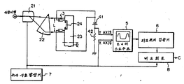
제4도는 본 발명의 제1실시예에 의한 1차입자비임 조사장치의 구성도.4 is a block diagram of a primary particle beam irradiation apparatus according to a first embodiment of the present invention.
제5도는 제4도내의 2차이온센서근처의 구성 측면도.5 is a side view of the configuration near the secondary ion sensor in FIG.
제6도는 2차입자들에 의해 형성된 신호로서 2차이온 신호를 사용하는 경우와 2차 전자신호를 사용하는 경우의 비교 설명도.6 is a comparative explanatory diagram of the case of using the secondary ion signal as the signal formed by the secondary particles and the case of using the secondary electronic signal.
제7도는 제4도내의 모니터 스코우프위의 화면예를 설명하기 위한 도면.FIG. 7 is a diagram for explaining an example of a screen on a monitor scope in FIG. 4; FIG.
제8도는 본 발명의 다른 실시예에 의한 1차입자비임 조사장치내의 제4도의 장치와 다른 부분들의 구성도.8 is a block diagram of the apparatus and other parts of FIG. 4 in the primary particle beam irradiation apparatus according to another embodiment of the present invention.
제9도는 2차이온센서의 검출정보에 준하여 컴퓨터를 사용한 주사신호를 제어하는 경우의 상세한 구성의 일예를 나타낸 도면.9 is a view showing an example of a detailed configuration in the case of controlling a scan signal using a computer based on the detection information of the secondary ion sensor.
본 발명은 1차입자비임의 조사장치 및 그의 조사방법에 관한 것이며, 특히 이온주입등을 위해 이온비임과 같은 1차비임을 어떤 주사폭으로 회전하는 디스크위에 놓인 반도체 웨이퍼와 같은 타게트(target)위에 조사하는 1차입자비임의 조사장치 및 그의 조사방법에 관한 것이다.The present invention relates to a device for irradiating a primary particle beam and a method for irradiating the same, and in particular, to irradiate a primary beam such as an ion beam onto a target such as a semiconductor wafer placed on a disk rotating at a certain scan width for ion implantation or the like. A device for irradiating primary particle beams and a method for irradiating the same.
일반적으로, 반도체 웨이퍼들과 같은 타게트들위에 이온주입을 행할때에, 예를들어 MOS 트랜지스터의 임계전압치(Vth)를 제어할 때에 반도체 웨이퍼들내로 주입될 이온들의 투여량은 적고, 또한 적은 투여량에 의해서 이온비임의 전류는 0.1 마이크로암페어 내지 1또는 2마이크로 암페어의 저전류로 유지된다. 그에 의해 웨이퍼들에 주입되는 열의 양이 감소된다.In general, when ion implantation is performed on targets such as semiconductor wafers, for example, when controlling the threshold voltage value Vth of a MOS transistor, the dosage of ions to be injected into the semiconductor wafers is small and also a small dose. By the amount, the current in the ion beam is maintained at a low current of 0.1 microamps to 1 or 2 microamps. This reduces the amount of heat injected into the wafers.
이와 반대로, MOS 트랜지스터의 소오스 또는 드레인영역을 형성할때에 예를들어, 반도체 웨이퍼들내로 주입될 이온들의 투여량은 많다. 그러므로, 직접회로의 제조측면에서 볼 때 상기 임계전압을 제어할때와 동일한 처리능력을 주기 위해서는 이러한 고투여량에 따라서 이온빔의 전류는 약 10밀리 암페어로 큰 것이어야 한다. 그 결과, 웨이퍼들에 가해지는 전력 또는 열(이온빔전류 X 이온 비임가속전압으로 표현됨)은 예를들어 약 10밀리암페어들 200kV=2kW에 달한다.In contrast, when forming a source or drain region of a MOS transistor, for example, the dose of ions to be implanted into semiconductor wafers is large. Therefore, in order to give the same processing power as in controlling the threshold voltage from the manufacturing side of the integrated circuit, according to this high dose, the current of the ion beam should be large as about 10 milliamps. As a result, the power or heat applied to the wafers (expressed as ion beam current X ion beam acceleration voltage) amounts to, for example, about 10 milliamps 200 kV = 2 kW.
그러므로, 이온들을 전자의 주입(Vth제어를 위한 것임)시에, 웨이퍼들을 자리맞춤하여 고정시킨 다음 어떤 강도의 이온비임을 웨이퍼위에 라스터(raster)주사한다. 그에 의해 어떤 강도의 이온비임이 단일 라스터 주사에 의해서 각 웨이퍼들위에 조사되더라도 웨이퍼들에 가해지는 열량이 적다. 따라서, 온도의 상승이 비교적 작기 때문에 별 문제점이 발생되지 않는다.Therefore, upon implantation of ions (for Vth control), the wafers are aligned and fixed and then a raster scan of the ion beam of some strength onto the wafer. Thereby, the amount of heat applied to the wafers is small even if an ion beam of any intensity is irradiated onto the respective wafers by a single raster scan. Therefore, since the rise in temperature is relatively small, little problem occurs.
그러나, 웨이퍼들내에 이온들을 후자의 주입(소오스와 드레인영역들 형성을 위함)시에, 복수의 웨이퍼들을 올려 놓는 스테이지인 회전드럼의 측면위에 또는 회전디스크의 표면위에 배치한 다음, 적어도 웨이퍼영역들이 커버되도록 어떤 강도의 이온비임을 복수의 웨이퍼들위에 연속적으로 주사한다. 그러한 주사는 복수회(예를 들어, 수회에서 약 100회 정도)반복된다. 그러므로 웨이퍼들에 순간적으로 부여되는 열을 분산시킬 필요성이 발생된다. 이 경우에, 상기 회전드럼을 사용할 경우와 비교할 때 상기 회전디스크를 사용하는 경우가 회전장치의 기구로 인해서 디스크의 회전속도를 더 개선할 수 있고 또한 웨이퍼들에 가해진 전력(열)을 분산시키기가 그만큼 더 쉽다는 점에서 더 좋다. 그러므로 웨이퍼들에 가해지는 전력이 클수록 회전디스크를 사용하는 것이 더 유리하다However, upon implanting the ions into the wafers (to form source and drain regions), the ions are placed on the side of the rotating drum or on the surface of the rotating disk, which is a stage for placing a plurality of wafers, An ion beam of some intensity is continuously scanned onto the plurality of wafers to be covered. Such injections are repeated multiple times (eg several to about 100 times). Therefore, a need arises to dissipate the heat instantaneously imparted to the wafers. In this case, the use of the rotating disk can further improve the rotational speed of the disk due to the mechanism of the rotating device as compared with the use of the rotating drum and also disperse the power (heat) applied to the wafers. Better in that it is easier. Therefore, the greater the power applied to the wafers, the more advantageous it is to use a rotating disk.
즉, 이 경우에, 다수의 웨이퍼들을 회전디스크위에 원주방향에 따라 배치한 다음 일정강도의 이온비임을 일정거리(웨이퍼의 직경 방향의 폭보다 약간 넓은 거리)를 가로질러 왕복하면서 조사하여 복수의 웨이퍼들의 표면전체위에 조사한다. (따라서 디스크가 회전되기 때문에 이온비임은 복수의 웨이퍼들을 연속으로 조사하기 위해서 레코드의 흠을 따르는 것과 같은 경로를 따른다. 그에 의해 복수의 웨이퍼들을 포함하는 소정 영역들이 연속적으로 조사된다.) 이온비임의 왕복조사(주사)는 상술한 바와 같이 복수회 반복된다. 그에 의해서 웨이퍼들내에 주입된 이온들의 투여량은 소정의 고투여량이 된다. 이 경우에 상술한 바와 같이 소정 폭으로 복수회 이온 비임을 왕복이동시키는 대신에 회전디스크를 소정폭으로 복수회 왕복이동시키는 것을 생각할 수도 있는 것이다. 그러나, 일반적으로 전자의 기술은 고속 왕복이동이 가능하므로, 통상 전자의 수단이 채용된다. 소정폭으로 이온비임을 왕복이동시킬 때에, 이온비임은 각단계 소정폭으로 단계적으로 연속으로 이동하는 것이다. 즉, 만일 주사시에 한단계마다의 이동폭이![]()
![]()
![]()
![]()
그러나, 그러한 이온비임을 조사할때에, 회전디스크위의 복수의 웨이퍼들을 포함하는 조사영역들의 내원주측과 외주측(디스크의 방사상 방향으로)의 주입되는 영역에 차이가 생긴다. 그러므로, 각 단계의 이온비임의 주입시간(체류시간)이 동일한 경우에는 내원주측에서의 (단위영역당) 이온투여량이 외원주측의 이온투여량(단위영역당)보다 더 많아져서 단위 영역당 투여량이 균일하지 않게 되므로 이온비임의 이동속도(다시말하여, 각단계로 이온비임의 체류시간)의 변화를 필요하게 한다.However, when irradiating such an ion beam, there is a difference in the implanted area of the inner circumferential side and the outer circumferential side (in the radial direction of the disk) of the irradiation areas including the plurality of wafers on the rotating disk. Therefore, when the implantation time (retention time) of the ion beams in each stage is the same, the ion dose (per unit area) on the inner circumference side is higher than the ion dose (per unit area) on the outer circumference side, so that the dosage per unit area Since it is not uniform, it requires a change in the moving speed of the ion beam (ie, the residence time of the ion beam in each step).
이 경우에, 조사영역의 소정폭위에 균일한 양을 투여하도록 이온비임의 조사위치를 변화시키기 위한 주사신호의 파형이 체류시간의 변화에 따라 소정파형에 동기되어 변화된다면 문제가 없을 것이다. 그러나, 실제에 있어서 주사신호의 옵셋과 크기(소위 게인)는 이온비임의 조사폭을 변화시키게 되어 이온비임의 조사범위(예정된 폭이사)에 위치벗어남을 일으킨다. 또한, 이온비임의 조사 경로를 제어하기 위해서 사용되는 주사용 마그네트 등의 비선형성(예를들어 마그네트형태 또는 마그네트에서 발생되는 에징효과(edging effect)로 인함)은 주사용 마그네트들의 자장강도(즉, 이온비임의 조사위치)가 조사신호에 대하여 선형으로 변화되지 못하는 원인이 되어 결국 이온빔의 조사폭과 조사범위를 벗어나게 하는 원인이 된다. 그러므로, 웨이퍼들위의 이온비임의 투여량의 균일성이 나빠지고 또한 배치(batch)가 다를때마다 웨이퍼들위의 투여량의 재현성이 나빠진다.In this case, there will be no problem if the waveform of the scanning signal for changing the irradiation position of the ion beam to change the irradiation position of the ion beam so as to administer a uniform amount over the predetermined width of the irradiation area changes in synchronization with the predetermined waveform in accordance with the change of the residence time. In practice, however, the offset and magnitude (so-called gain) of the scanning signal change the irradiation width of the ion beam, causing the position to deviate from the irradiation range of the ion beam (predicted width director). In addition, nonlinearity (e.g., due to the magnet form or the edging effect generated in the magnet) used to control the irradiation path of the ion beam may be due to the magnetic field strength of the magnets for injection (i.e., Irradiation position of the ion beam) does not change linearly with respect to the irradiation signal, which in turn causes the ion beam to be out of the irradiation width and the irradiation range. Therefore, the uniformity of the dosage of the ion beam on the wafers is poor, and the reproducibility of the dosage on the wafers is poor each time the batch is different.
이러한 문제점들에 비추어, 종래에는 디스크의 방사상 방향으로의 주입영역에서의 차이와 주사용 마그네트들의 불균일성을 예를들어 테스트웨이퍼들을 사용하여, 반경 방향에 대해서 이온주입맵(map)을 만들어 두고(예를 들어 쉬트저항에 의해 이를 측정하여), 또한 주사용 마그네트들의 자장변화량 또는 자장강도를 보정하도록 맵에 준하여 사전에 소프트웨어에 의해서 프로그램된 소정의 주사신호를 사용하여 보정하였다.In view of these problems, conventionally, an ion implantation map is made in the radial direction using test wafers, for example, the difference in the injection region in the radial direction of the disk and the nonuniformity of the scanning magnets (e.g., It was corrected by using a predetermined scan signal programmed by software in advance in accordance with the map to correct the magnetic field change amount or the magnetic field intensity of the magnets for scanning).
그러나, 이러한 방법으로도 실제에 있어, 웨이퍼들위에 조사된 이온비임의 조사위치(엄밀히 말해서 장치의 운전시마다 즉 배치마다 다름)가 검출되지 않으므로 엄밀히 말해서 장치의 운전시마다 다른 주사용 마그네트들의 비선형성과 주입영역의 차이로 인하여 발생되는 투여량의 비균일성을 완전히 보정할 수는 없다.However, even in this manner, since the irradiation position of the ion beam irradiated on the wafers (strictly, every operation of the device, that is, every batch) is not detected in practice, strictly speaking, non-linearity and implantation of different scanning magnets for each operation of the device It is not possible to fully compensate for the non-uniformity of the dosages generated due to differences in the areas.
본 발명은 상술한 문제점들을 해결한다는 관점에서 행해진 것이며 그의 목적은 장치의 각 운전시마다 이온비임의 주사범위와 조사폭(반경방향에서의 조사위치)을 소정의 조사폭과 소정조사위치로 정밀하게 제어함으로써 웨이퍼들위에 투여되는 이온비임의 불균일성과 각 배치의 웨이퍼들위의 투여량의 재현성을 개선하는 데 있다.The present invention has been made in view of solving the above problems, and its object is to precisely control the scanning range and irradiation width (irradiation position in the radial direction) of the ion beam to a predetermined irradiation width and predetermined irradiation position for each operation of the apparatus. This improves the nonuniformity of the ion beam administered on the wafers and the reproducibility of the dosage on the wafers in each batch.
상술한 목적을 달성하기 위해, 본 발명의 한 태양에 의하면, 타게트가 놓이는 스테이지와, 1차 입자비임으로 스테이지위의 소정 주사영역을 조사하기 위한 수단과, 1차 입자비임의 조사에 의해서 발생되는 2차 이온을 스테이지 또는 타게트로부터 검출하기 위한 2차 이온센서와, 그리고, 2차 이온센서로부터의 출력신호에 준하여 조사수단을 제어하기 위해 조사수단과 2차 이온센서에 연결되는 수단을 포함하는 1차 입자비임 조사장치가 제공된다.In order to achieve the above object, according to one aspect of the present invention, there is provided a stage on which a target is placed, means for irradiating a predetermined scanning area on the stage with the primary particle beam, and generated by irradiation with the primary particle beam. A secondary ion sensor for detecting secondary ions from the stage or target, and means connected to the irradiation means and the secondary ion sensor to control the irradiation means in accordance with an output signal from the secondary ion sensor A primary particle beam irradiation apparatus is provided.
또한, 본 발명의 다른 태양에 의하면, 타게트의 표면근처에 설비된 2차 이온센서의 출력을 사용하여 소정폭 또는 소정영역위의 타게트위에 주사되는 1차입자 비임의 조사위치를 검출하는 단계와, 검출된 조사위치에 관한 정보에 준하여 조사위치의 벗어남을 보정하는 단계와, 그리고 보정단계에서 얻어진 정보에 준하여 타게트의 표면을 조사하도록 1차입자비임을 주사하는 단계를 포함하는 1차입자비임의 조사방법이 제공된다.Further, according to another aspect of the present invention, detecting the irradiation position of the primary particle beam to be scanned on the target of a predetermined width or a predetermined area using the output of the secondary ion sensor installed near the surface of the target, and detecting There is provided a method for irradiating a primary particle beam comprising correcting the deviation of the irradiation position according to the information on the irradiated position, and scanning the primary particle beam to irradiate the surface of the target based on the information obtained in the correcting step. do.
본 발명의 상기 구성에 의하면, 방향성을 갖는 2차이온센서는 센서가 설치되는 위치에 대응하는 타게트(디스크 또는 웨이퍼) 부분위에 조사되는 1차 입자비임으로 인해서 발생되는 (1차입자비임의 반사로 인해 또는 1차입자 비임의 조사에 의해서, 조사위치에서 타게트 재료의 스퍼터링으로 인해 발생되는)2차 이온들을 선택적으로 검출하는데 사용된다. 이에 의해, 그것을 1차입자임을 주사하기 위한 주사신호와 1차입자비임의 주사위치간에 만족스러운 일치가 이루어졌는지를 연속적으로 검출한다. 그 검출결과에 따라, 1차입자비임의 주사시스템은 소정의 보정을 행하도록 제어된다(예를들어, 조정은 주사용 마그네트의 자장형성을 위해 미리 프로그램된 주사신호로 이루어진다). 그에 의해서 1차입자비임의 주사폭과 반경향에서의 1차입자비임의 조사위치는 고도의 정밀도로 조정되므로, 타게트들에 대한 이온빔 투여량의 균일성과 각 배치마다의 웨이퍼들에 대한 이온빔 투여량의 재현성이 확보된다.According to the above configuration of the present invention, the secondary ion sensor having the orientation is generated due to the primary particle beam irradiated on the target (disk or wafer) portion corresponding to the position where the sensor is installed (due to the reflection of the primary particle beam). Or by irradiation of the primary particle beam, to selectively detect secondary ions (generated due to sputtering of the target material at the irradiation position). This continuously detects whether a satisfactory match is made between the scan signal for scanning it as the primary particle and the dice of the primary particle beam. According to the detection result, the scanning system of the primary particle beam is controlled to perform a predetermined correction (e.g., the adjustment is made of a scanning signal preprogrammed for the magnetic field formation of the scanning magnet). Thereby, the scanning width of the primary particle beam and the irradiation position of the primary particle beam in the radial direction are adjusted with high precision, so that uniformity of the ion beam dosage for the targets and reproducibility of the ion beam dosage for the wafers in each batch are achieved. This is secured.
또한, 본 발명의 조사방법에 의하면, 첫 번째 주사에 의해서 타게트위에 조사되는 (예, 이온주입)1차입자비임의 위치는 2차이온센서의 출력에 의해서 검출된다. 검출된 조사위치의 정보에 준하여 1차입자비임의 조사위치의 벗어남이 검출된다. 이 검출된 정보에 준하여 주사신호가 보정되며, 이 보정된 주사신호는 타게트위의 1차입자비임의 두 번째 조사용으로 사용된다. 동일한 단계들이 소정회 반복한다. 이 경우에, 각 조사단계와 그의 위치벗어남의 보정이전에 행해지는 전단계의 조사위치의 검출이 최종주사시까지 매번 수행할 수도 있으며, 또는 먼저 소정횟수를 반복한 후에 검출과 보정을 생략하여 조사를 연속적으로 반복할 수도 있다.In addition, according to the irradiation method of the present invention, the position of the primary particle beam irradiated (eg, ion implanted) onto the target by the first scan is detected by the output of the secondary ion sensor. Deviation from the irradiation position of the primary particle beam is detected based on the detected irradiation position information. The scanning signal is corrected in accordance with the detected information, and the corrected scanning signal is used for the second irradiation of the primary particle beam on the target. The same steps are repeated a predetermined time. In this case, the detection of the irradiation position of the previous stage performed before each irradiation step and its positional deviation correction may be performed each time until the final scan, or the detection and correction are omitted after repeating the predetermined number of times first. It may be repeated continuously.
이는 임의로 선택할 수 있다.It can be chosen arbitrarily.
본 발명은 보정을 좀더 정밀하게 행하기 위하여 상술한 종래의 소프트웨어 보정후에 사용되는 추가수단을 존재시킬 수도 있는 것이다.The present invention may have additional means to be used after the conventional software correction described above to make the correction more precise.
본 발명을 명료히 이해하기 위해서 우선 종래의 회전디스크를 사용하는 1차입자비임 조사장치에 관한 설명을 하겠다. 제1a도는 종래의 1차입자비임 조사장치의 전체구성의 일예를 나타내고 있다. 여기서 10과 11은 서로 내외로 형성된 외부 및 내부하우징들을 나타낸다. 하우징들(10,11)은 그들 사이에 연결된 이온가속을 위한 전류전원 (12)(예를 들어 0V로부터 120kV내지 175kV까지의 범위로 조정됨)을 갖고 있다. 이온발생원 (15)에는 플라스마를 발생시키기 위한 전원장치 (13)가 연결되어 있다. 전력공급장치(13)의 하우징과 내부하우징(11)과의 사이에는 예를들어 25내지 80kV의 직류전원 (14)이 연결되어 있다. 참조번호 16은 이온들을 끌어내기 위한 전극이고 예를 들어 하우징 (11)과 동일전위로 설정된다. 이에 의해서 이온발생원 (15)과 추출전극 (16)간에서 직류전원 (14)을 사용하여 강한 전계가 발생된다.In order to clearly understand the present invention, first, a description will be given of a primary particle beam irradiation apparatus using a conventional rotating disk. 1A shows an example of the overall configuration of a conventional primary particle beam irradiation apparatus. Where 10 and 11 represent external and internal housings formed in and out of each other. The
그 결과로, 이온발생원(15)에서 발생되는 플라스마 이온들의 비임은 추출전극(16)을 거쳐서 끌려나온 다음, 도면의 지면에 대해서 수직방향으로 서로 대향하여 배치되는 한쌍의 원호형 마그네트(17)(도면 1a도에는 하측전극 하나만 보임)의 간극을 통하여 통과한 다음, 그 간극에 형성된 자장의 작용에 의해서 이온비임의 전진방향이 굽혀진다. 이 경우에, 이온비임을 포함하는 소자의 종류 (즉, 이온중량)에 따라 굽힘정도가 다르므로(이온이 가벼울수록 굽힘이 큼)소정의 소자에 대응하는 이온비임만이 슬릿(18)을 통해 통과하도록 소정의 경로를 통해 앞으로 통과한 다음, 이중 하우징들(10,11)간에 구비된 가속관(19)내에서 직류전원(12)에 의해서 발생되는 강한 전계에 의해서 가속된 다음, 소정 타게트 (예를 들어 박스하우징(20)내의 회전디스(23)위에 놓인 반도체웨이퍼들(24))를 향해 조사된다. 이온비임의 경로가 형성되는 하우징(11), 가속관(19) 및 하우징(20)은 진공용기로서 형성된다.As a result, the beam of plasma ions generated in the
이 경우에, 원주방향으로 회전디스크(23)위에 놓인 다수의 웨이퍼들(24) (제1b도를 참조)의 표면전체에 이온비임이 조사되도록, 이온비임은 소정폭(예, 제1b도에 나타낸 것과 같이 반도체웨이퍼들(24)을 포함하는 반도체웨이퍼들(24)의 폭보다 약간 더 넓은 폭(L)에 결쳐서 조사되어야 한다(그러므로, 디스크의 회전으로 인해서, 조사영역이 제1b도에서 빗금친 점선들로 나타낸 영역(S)이 된다). 이러기 위한 수단으로서,(1) 소정폭(L)으로 왕복으로 회전디스크(23)를 이동시키거나 또는 (2) 이온비임을 소정폭(L)으로 왕복이동 시켜서 타게트위에 이온비임의 조사를 반복하는 것을 생각할 수 있다. 이 경우에, 후자(2)는 고속으로 주사 할 수 있다.In this case, the ion beam has a predetermined width (e.g., in FIG. 1b) so that the ion beam is irradiated on the entire surface of the plurality of wafers 24 (see FIG. 1b) placed on the
제2도는 이온비임의 조사를 위해 후자(2)의 수단을 사용하는 경우에 이온빔이 가속관(19)을 통하여 통과한 후에 타게트위에 조사될때에 상기 주사를 행하기 위한 구체적인 구성의 일예를 나타낸다. 도면에서, 21은 이온비임이 소정범위의 각도(θH)에 걸쳐서 왕복하여 주기적으로 이동하게 해주기 위한 주사용 마그네트들을 나타내며, 22는 상술한 바와 같이 주사용 마그네트(21)로 인해서 그의 진행방향으로 굽혀진 이온비임을 소정 방향과 평행하게 해줌으로써 그에 의해 링(25)에 의해 디스크(23)위에 장착된 웨이퍼들의 영역을 포함하는 소정주사폭(L)의 범위내에서 이온비임을 회전디스크(23)위에서 왕복으로 이동시켜 주기 위한 마그네트들을 나타낸다.2 shows an example of a specific configuration for performing the scan when the ion beam is irradiated onto the target after passing through the
여기서, 마그네트들(21,22)은 마그네트(17)와 같이 각각 제 2도의 예에서는 상하 방향으로 서로 대향하는 마그네트쌍을 구성한다. 마그네트(21)은 소정의 주사신호에 의해 여기되어 마그네트쌍들 간의 간극내에서 생기는 자장의 강도를 주기적으로 변환시킨다. (그 간극을 통하여 이온비임이 통과됨)이에 의해서 이온비임은 소정범위의 각도(θH)에 걸쳐서 반복적으로 주사된다. 마그네트(22)는 그들간의 간극내에서 생기는 자장의 강도를 일정하게 해준다. 상술한 바와 같이, 상기 마그네트들(21)을 사용함으로써, 이온비임은 소정범위의 각도(θH)에 걸쳐서 왕복으로 이동하도록 여러 가지 각도로 굽혀진다. 또한, 제2도의 실시예에서 마그네트들(21)간의 간극내에서 생기는 자장의 방향과 반대방향으로 마그네트들(22)간의 간극내에서 생기는 자장의 방향을 만들어 줌으로써 원래의 방향으로 빔이 진행하게 된다.Here, the
또한 제2도에 나타낸 바와 같이 마그네트들(22)로서 아래로 갈수록 형성되는 마그네트(22)의 폭이 넓은 예를 들면, 삼각형 모양이 사용된다. 그 결과로, 굽혀진 모든 이온비임들은 소정 방향으로 평행하게 향하게 된다.Also, as shown in FIG. 2, a wider, for example, triangular shape of the
제3도는 원주방향을 따라 상기 회전디스크(23)위에 놓인 복수의 웨이퍼들(24)(이 경우에 웨이퍼가 10개임)의 표면전체에 이온비임을 조사하도록 소정폭(L)에 결쳐서 이온비임을 조사할 경우 (따라서, 조사영역은 상술한 바와 같은 빗금점선들로 나타낸 영역(S)이 된다)로서 이온비임의 이동속도를 설명하기 위한 도면이다. 여기서, 상술한 바와 같이 회전디스크 반경방향에 걸쳐서 이온비임을 왕복 이동시킬때에 이온비임은 각각 소정폭(△W)으로 단계적으로 연속적으로 이동하도록 만든다.3 shows the ion beam at a predetermined width L so as to irradiate the ion beam on the entire surface of the plurality of wafers 24 (in this case, 10 wafers) placed on the
이온비임을 이러한 방법으로 회전디스크의 방경방향으로 왕복이동하게 할 때에 상술한 바와 같이 조사영역의 내원주측과 외원주측간의 주입영역에서 차가 발생된다. 예를 들어, 최내원주띠로 형성되는 영역(S2)의 면적은 영역(S2)의 원주길이와 단계마다의 이동폭(![]()
![]()
![]()
![]()
![]()
![]()
여기서, n : 왕복이동횟수Where n is the number of round trips
Iв: 이온비임의 전류Iв: current of ion beam
![]()
![]()
q : 이온전하q: ion charge
![]()
![]()
R : 띠모양의 영역들의 반경R is the radius of the banded regions
따라서, 띠모양의 영역들내의 투여량(D)을 균일하게 만들기 위해서(제3도에서, 본래 투여하고져하는 투여량(Ds) 제3도에서 선ι로 나타낸 것과 같은 체류시간(![]()
![]()
![]()
![]()
그러므로, 예를 들어, 실제의 조사범위가 회전디스크의 중심방향으로 벗어날때는 소정위치에서의 체류시간은 벗어남의 크기에 따라서 증가된다. 그 결과로 회전디스크의 반경방향으로의 투여량은 제3도에서 D'로 나타낸 것과 같이 변화된다. 한편, 역으로 실제의 조사범위가 회전디스크의 외향으로 벗어날 때에는 회전디스크의 반경방향으로의 투여량은 제3도에서D"로 나타낸 것과 같이 변화한다.Therefore, for example, when the actual irradiation range deviates in the direction of the center of the rotating disk, the residence time at a predetermined position increases with the magnitude of the deviating. As a result, the radial dose of the rotating disk is changed as indicated by D 'in FIG. On the other hand, when the actual irradiation range deviates outward of the rotating disk, the dose of the rotating disk in the radial direction changes as indicated by D ″ in FIG.
또한, 상술한 바와 같이 이온비임들을 주사하는 주사용 마그네트들의 비선형성은 주사신호에 대해서 주사용 마그네트의 자장강도를 직선적으로 변화시키지 못하는 원인이 될 수 있다. 그 결과로, 체류시간(![]()
![]()
본 발명은 상술한 문제점들을 해결하기 위한 것이다.The present invention is directed to solving the above problems.
제4도는 본 발명의 제1실시예에 의한 1차입자비임조사장치의 구성을 나타내고 있다. 제4도에 나타낸 바와 같이 가속관에 의해서 가속되는 이온비임은 주사용 마그네트(21)와 보정용마그네트(22)사이를 통과한 후에, 웨이퍼들(24)을 포함하는 디스크(23)위의 소정영역에 걸쳐서 조사된다. 주사용 마그네트(21)는 주사를 위해 소정의 자장을 형성하도록 주사신호발생기(7)로부터 공급되는 사전에 프로그램된 주사신호에 의해서 여기된다.4 shows the configuration of the primary particle beam irradiation apparatus according to the first embodiment of the present invention. As shown in FIG. 4, the ion beam accelerated by the accelerator tube passes between the
참조번호 3은 방향성을 갖는 2차이온센서이다.
제4도에 나타낸 실시예에서는 2개가 설비되어 있는데 그들 각각은 웨이퍼(24)의 단부들에 인접한 디스크(23)의 부분들에 위치하고 있다(그러므로, 소정폭(L)을 갖는 조사영역의 단부분들 근처에 있음)요약하면, 2차이온센서들로서, 센서의 전극들이 검출될 조사위치근처에 배치될 수 있다. 센서전극들로서 간단한 금속편들을 사용할 수 있고 또는 제5도에 나타낸 것과 같은 전극들 (32)을 정해진 원통형커버들(31)내에 설비할 수도 있다. 전극들(32)은 커버들(31)과 절연되어 있다(예, 유리로 커버들을 만든다).In the embodiment shown in FIG. 4, two are provided, each of which is located in the portions of the
제4도는 위에서 본 도면이다.4 is a view from above.
이온비임(1차 이온비임)이 소정 타게트(웨이퍼들(24)을 포함하는 소정 디스크영역)위에 조사될때에 조사되는 타게트부분으로부터 소위2입자들이 발생된다. 여기서, 2차입자들은 2차이온들 또는2차전자들 및 광자를 포함한다. 그러나 본 발명에서는 조사된 타게트부분으로부터 발생되는 2차이온들이 검출된다.When the ion beam (primary ion beam) is irradiated onto a predetermined target (a predetermined disk region including the wafers 24), so-called second particles are generated from the target portion to be irradiated. Here, secondary particles include secondary ions or secondary conductors and photons. However, in the present invention, secondary ions generated from the irradiated target portion are detected.
이에 대한 이유는 제6도에 나타낸 바와같이 2차 전자들이 검출될때에 2차전자신호(Se)의 피크치(V2)센서의 설치위치근처의 타게트부분으로부터 방출되는 2차전자들로 인하여)는 2차이온들(예, 양이온들)이 검출될 경우의 2차이온신호(Si)의 피크치(V1)보다 신호강도에 있어서 훨씬 더 크게 되기 때문이다(제6도에 강도의 비율이 정확히 도시되지 않았지만, V2와 V1간의 비는(통상적으로 10:1 정도로 사용된다). 그러나, 2차전자신호는 타게트의 두 단부들에 설비된 2개의 센서들에 대응하는 양측의 피크치들 사이에서 피크치들의 어느 부분값인 잡음신호(V2')가 혼합됐다. 결과적으로, 편편하고, 안정된 신호가 2차이온신호의 경우에서와 같은 피크치 이외에서는 얻을 수 없으므로 검출위치에서 오차의 변화가 생긴다. 2차이온들은 타게트부분에서 조사된 1차이온들의 반사에 의해서 발생된 것들과 조사위치에서 타게트재료의 스퍼터링으로 인해서 발생된 것들을 포함한다.The reason for this is that, as shown in FIG. 6, when secondary electrons are detected, due to the secondary electrons emitted from the target portion near the installation position of the peak value V2 sensor of the secondary electron signal Se is 2). This is because the difference in signal intensity is much larger than the peak value V1 of the secondary ion signal Si when the difference ions (e.g. cations) are detected (although the ratio of intensity is not exactly shown in FIG. The ratio between V2 and V1 (typically 10: 1 is used), however, the secondary electron signal is the portion of the peaks between the peaks on both sides corresponding to the two sensors mounted at the two ends of the target. The result is a mixed noise signal (V2 '), which results in a change in the error at the detection position, since a flat, stable signal cannot be obtained outside the peak value as in the case of the secondary ion signal. Primary Ion Irradiated at Part Those caused by the reflection of the research locations include those occurring due to sputtering of materials tageteu.
또, 주목할 것은 스퍼터링된 타게트 재료는 조사위치에서의 디스크재료(예, 알미늄)와 웨이퍼 재료(예, 실리콘)를 포함하고, 그 어느것이냐는 2차이온센서들이 설치된 위치에 따라서 다르다는 것이다.Note that the sputtered target material includes a disk material (eg aluminum) and a wafer material (eg silicon) at the irradiation position, which depends on the position where the secondary ion sensors are installed.
여기서, 2차이온센서(3)내에 설비되고 타게트와 격리되어 있는 전원(41) 또는 밧데리로 음으로 바이어스된 전극(32)은 2차이온센서(3)가 설치된 위치에 대응하는 타게트부분(제5도에서 참조문자 "a" 참조)으로부터 발생되는 양(+)의 2차이온들만 유입되는 것을 받아들인다(즉, 방향성을 갖는다). 다시말하면, 2차이온센서(3)는 상기 타게트부분 "a"위에 1차이온비임의 조사에 의해서 발생되는 2차이온들만을 취하므로 소위 방향성을 갖는 것이다.Here, the
이러한 식으로 2차이온센서(3)의 전극(32)내로 취해진 2차이온들(이 경우에, 양이온들)의 전하들은 바이어스전원(41) (에, 전극(32)에 -10V 내지 -100V의 부(-)의 바이어스 전압이 인가됨)으로부터의 바이어스전압에 준하여 바이어스전원(41)과 전향(42)을 거쳐서 접지측으로 흐르므로 저항(42)의 양단에는 취해지는 2차이온들의 양에 비례한 전압강하가 발생된다. 디스크(23)는 통상 접지전위로 되는 것이다.In this way, the charges of the secondary ions (in this case, the cations) taken into the
참조번호 5는 모니터 스코우프로서 그의 X축 입력으로서 주사신호발생기(7)로부터 상술한 주사신호를 수신하고 또한, YM축 입력으로서 바이어스전원(41)과 저항(42)간의 연결점의 전위 Vo를 수신한다. 따라서, 제7도에 나타낸 것과 같이 모니터 스코우프(5)는 그의 횡축에 주사용 마그네트(21)를 여기시키는 주사신호(B)의 값을 취하고(주사신호의 변화에 따라, 주사용 마그네트(21)의 자장의 강도가 변화되고, 이온비임의 조사위치가 변화된다)종축에 주사신호(B)의 값에 대응하는 2차이온센서의 출력(S)을 취한 화면을 그린다.
다시말하여, 제7도의 화면은 주사신호의 값이 B1과, B2일때의 피크치들이 2차이온센서의 출력(S)에 발생됨을 나타낸다(즉, 이온비임은 2차이온센서(3)의 설치위치에 대응하는 타게트부분 "a"에 조사되고 또한, 2차이온센서(3)에 취해진 2차전자이온들은 피크가 된다).In other words, the screen of FIG. 7 shows that peak values when the scan signal is B 1 and B 2 are generated at the output S of the secondary ion sensor (that is, the ion beam is the secondary ion sensor 3). The secondary electron ions irradiated to the target portion "a" corresponding to the installation position of the
참조번호 6은 피크위치들에 대응하는 주사신호들의 값들(B1', B2')을 검출하는 피크위치 검출기를 나타낸다. 또한 8은 비교회로이고 주사신호발생기(7)로부터 공급되는 주사신호의 값으로부터 주사신호값들(B1',B2')을 찾아내어 그들을 이상적인 값(B1,B2)과 비교하여 B1'와B2'가 2차이온센서(3)의 출력이 본래 피크가될 주사신호의 값들 (B1,B2) (즉,2차이온센서의 설치위치에 대응하는 타게트부분을 조사하도록 하는 주사신호의 값들)과 일치하는 지의 여부를 상시 판별한다.Reference numeral 6 denotes a peak position detector for detecting values B 1 ′, B 2 ′ of the scan signals corresponding to the peak positions. In addition, 8 is a comparison circuit and scan signal values B 1 ′, B 2 ′ are found from the values of the scan signals supplied from the scan signal generator 7, and they are compared with the ideal values B 1 , B 2 to B. 1 'and B 2 ' are the values of the scan signal (B 1 , B 2 ) where the output of the
비교회로(8)로부터의 출력(C)에 의해서 불일치함이 판별된 때에는 주사시스템은 인터록되거나 또는 일치 될 때까지 소정의 귀환수단에 의해서 조정하여, 주사신호발생기(7)로부터 출력된 주사신호의 값을 주사폭 또는 주사위치의 벗어남을 보정하도록 한다. 예를들어, 제7도에 나타낸 것과 같이 피크위치들에 대응하는 주사신호의 값이 B1'와 B2'인데 대하여 만일 2차이온센서의 출력이 본래 피크가 되어야할 주사신호값(B1,B2)이면, 주사신호발생기(7)로부터 출력되는 주사신호의 값들(B1,B2)은 증가되어 상기 B1' 및 B2'와 일치 되도록 보정된다.When a discrepancy is determined by the output C from the comparison circuit 8, the scanning system adjusts by a predetermined feedback means until it is interlocked or coincident, so that the scan signal output from the scan signal generator 7 The value should be compensated for deviations in scan width or dice. For example, the seventh degree, the value of the scanning signal B 1 'and B 2' it inde about ten thousand and one second output the scanning signal value that is to be the original peak of the difference on the sensor corresponding to the peak position as shown in (B 1 , B 2 ), the values B 1 and B 2 of the scan signal output from the scan signal generator 7 are increased and corrected to match B 1 ′ and B 2 ′.
제4도에 나타낸 실시예에서는 모두 두 개의 2차이온센서들(3)이 설비되어 있다. 그들은 각각 소정주사영역폭의 양단부 근처에 설치되어 있으나, 설치되는 센서들의 수는 특별히 제한되지 않는다. 예를들어, 그것은 주사영역의 한쪽부근에만 설치할 수도 있다. 또한, 제8도에 나타낸 실시예에서 2개의 2차이온센서(3',3")예를 들어 주사영역의 양단부의 각단부 근처에 비임직경정도 떨어져서 이온비임의 주사방향에 대응하는 위치에 설치되어 있다.In the embodiment shown in FIG. 4, both
상술한 두 단부들 근처의 내측 2차이온센서들(3')과 외부 2차이온센서들(3")에 의해서 검출된 2차이온출력은 상기와 동일한 방식으로 바이어스전원(41')과 저항(42')으로 구성되는 회로와 바이어스전원(41")과 저항(42")으로 구성되는 회로를 각각 거쳐 2현상 모니터 스코우프(dual trace monitor scope)(5')의 Y1축 입력과 Y2축 입력으로서 공급된다. 이때에 2현상 모니터 스코우프(5')의 X-축입력으로서, 제4도의 실시예와 동일한 방식으로, 주사신호발생기(7)로부터 출력되는 주사신호가 공급된다. 이렇게 하면 2현상모니터 스코우프(5')에는 2차 이온센서들(3',3")의 출력들을 종축에 주사신호(B)의 값을 수평축에 위한 상호 접근된 2개의 파형들이 나타난다.The secondary ion output detected by the inner secondary ion sensors 3 'and the outer
따라서, 주사신호들의 값이 2개의 파형의 피크들의 교차점들에 대응하는 2차이온센서들의 출력들(B1', B2')을 만들때에 이온비임이 주사영역의 양단부 근처에 배치된 2개의 2차이온센서들(3',3")간의 위치에서 조사되고 있다고 판단하여 상기와 같은 보정을 행하고 또한, 교점들의 검출에 의해서 피크위치들의 검출을 더 정확하게 행할 수 있다.Thus, when the value of the scan signals makes the outputs B 1 ′, B 2 ′ of the secondary ion sensors corresponding to the intersections of the peaks of the two waveforms, an ion beam is placed near both ends of the scan area. It is judged that the position is irradiated at the position between the two
또한, 주사영역내에 복수의 2차이온센서들을 선상으로 또는 면상으로 배열하고, 또한 소정의 모니터장치(예, 상술한 실시예에 나타낸 것고 같은 모니터회로 또는 단순한 비교회로)에 의해서 2차이온센서들의 출력들을 모니터링함으로써, 이온비임의 조사위치를 연속적으로 검출하고 또한, 그와 동시에 좀더 정밀하게 이온비임의 강도분포를 검출할 수 있다.In addition, a plurality of secondary ion sensors may be arranged in a line or plane in the scanning area, and also by a predetermined monitor device (e.g., a monitor circuit or a simple comparison circuit as shown in the above-described embodiment) of the secondary ion sensors. By monitoring the outputs, it is possible to continuously detect the irradiation position of the ion beam and at the same time detect the intensity distribution of the ion beam more precisely.
상기 실시예들에서는 타게트위에 조사되는 1차입자비임이 이온비임인 경우를 설명하였으나 본 발명에 의해서 커버되는 1차비임은 중성비임일 수도 있다. 이 경우에, 중성비임은 상술한 바와 같이 주사된 이온비임을 예를들어 부유가스(free floating gas)를 통과시키는 수단에 의해서 중성화시킬 수 있다. 이렇게하여 생긴 중성비임이 소정의 타게트위에 조사될때에 조사되는 타게트부분에서 발생되는 2차이온들은 상기 실시예들과 동일한 방식으로 중성비임의 조사위치를 검출할 수 있도록 2차이온센서(3)에 의해서 검출될 수 있다.In the above embodiments, the case where the primary particle beam irradiated on the target is an ion beam has been described, but the primary beam covered by the present invention may be a neutral beam. In this case, the neutral beam can be neutralized by means of passing a free floating gas, for example, the ion beam injected as described above. The secondary ions generated in the target portion to be irradiated when the generated neutral beam is irradiated onto a predetermined target are applied to the
또한, 중성비임의 양은 2차이온센서의 출력에 의해서 전기적으로 검출될 수 있다. 조사위치와 비임의 양에 대해서 소정의 보정을 행할 수 있다.Also, the amount of neutral beam can be detected electrically by the output of the secondary ion sensor. Predetermined correction can be made to the irradiation position and the amount of beam.
제9또는 2차이온센서들에 의해서 검출된 정보에 준하여 컴퓨터를 사용하여 주사신호의 값을 제어할 경우의 상세한 구성의 일예를 나타내고 있다. 제4도의 것들에 대응하는 부분들은 동일한 참조번호들을 부여했다.An example of the detailed configuration in the case of controlling the value of the scan signal using a computer based on the information detected by the ninth or secondary ion sensors is shown. Parts corresponding to those in FIG. 4 have the same reference numerals.
2차이온센서로부터 출력되는 아나로그신호는 센서들의 출력측에 연결된 바이어스전원(41)과, 저항(42)간의 연결점으로부터 게인최적화기(91)와 제1A/D변환기(92)를 거쳐서 수사폭 최적화기(9)에 구비된 CPU(94)로 공급된다. 또한, 도우스(dose)CPU(71) (상기 주사신호발생기(7)에 대응함)로부터 출력되는 주사신호는 제2A/D변환기 (93)을 거쳐서 동일한 방식으로 상기 CPU(94)로 입력된다.The analog signal output from the secondary ion sensor is optimized through the
상기 게인 최적화기(91)에서, 게인은 바이어스전원(41)과 저항(42)간의 연결점에서 취한 전위의 피크치(투여량에 따라 1차이온비임의 강도에 의해서 변화됨)는 A/D변환기(92)에 대한 입력으로서 적합한 소정의 값이 된다.In the
A/D변환기들(92,93)로부터 출력된 디지털신호들은 CPU(94)로 입력된다. CPU(94)는 2차이온센서들의 피크출력들에 대응하는 주사신호들의 값들을 검출하여, 보정값(즉, 1차이온비임의 조사위치의 벗어남)을 계산한 다음 위치의 벗어남을 주사신호의 게인과 옵셋으로 변환(주사신호 전압 V와 체류시간![]()
![]()
최종 계산된 보정 신호들은 D/A변환기(95)를 거쳐서 게인에 대응하는 주사게인신호로서 그리고 옵셋에 대응하는 주사밸런스신호로서 주사제어기(72)로 각각 입력된다. 이에 의해, 도우즈 CPU(71)로부터 주사제어기 (72)로 입력되는 주사신호입력의 게인과 옵셋은 주사게인신호와 주사밸런스신호에 의해 보정된다.The final calculated correction signals are input to the
보정된 주사신호는 주사전원(73)을 통하여 소정의 주사신호전류가 되어 주사용 마그네트(21)에 공급된다.The corrected scan signal becomes a predetermined scan signal current through the
CPU(94)내에 계산된 조사위치의 벗어남의 보정량(게인과 옵셋)은 필요에 따라 디스플레이되고 또한, 데이터기입기(96참조)에 의해 기록된다.The amount of correction (gain and offset) of the deviation of the irradiation position calculated in the CPU 94 is displayed as necessary and recorded by the data writer 96 (see).
다음에, 1차입자비임조사장치를 사용하는 회전디스크위에 위치되는 반도체 웨이퍼들위에 이온비임을 주사 및 조사함으로서 실제로 이온주입하는 경우의 공정에 관해서 설명하겠다.Next, a process in the case of actually implanting ions by scanning and irradiating ion beams on semiconductor wafers positioned on a rotating disk using a primary particle beam irradiation apparatus will be described.
이 경우에, 우선 1회째 주사에 의해서 타게트위에 조사되는(이온주입되는) 1차 입자비임의 조사위치는 2차이온센서에 의해 검출된다. 조사위치에 관한 첫 번째로 검출된 정보에 준하여 1차입자비임의 조사위치의 벗어남이 보정된다. 주사신호를 상기 위치 벗어남에 따라 보정되는 2회째주사에 의해서 타게트위에 1차입자비임의 2회째조사(이온주입)가 행해지는 동시에, 위치벗어남의 두 번째 데이터를 3회째 주사이전에 얻어 보정한다. 이와같은 단계가 소정 횟수 반복된다.In this case, first, the irradiation position of the primary particle beam irradiated (ion injected) onto the target by the first scanning is detected by the secondary ion sensor. The deviation of the irradiation position of the primary particle beam is corrected based on the first detected information about the irradiation position. The second scan (ion injection) of the primary particle beam is carried out on the target by the second scan corrected according to the deviation of the scan signal, and the second data of the positional deviation is obtained and corrected before the third scan. This step is repeated a predetermined number of times.
이 경우에, 검출과 보정단계를 1회만 행하지 않는 이유는 측정시스템내에서 발생되는 오차들에 준하여 주사신호를 보정하는 위험이 있기 때문이다. 이러한 이유 때문에 안전성을 고려하여, 주사신호의 보정은 적어도 초기 수회조사(이온주입)하는 동안의 각 조사단계때마다 행해진다.In this case, the reason why the detection and correction steps are not performed only once is that there is a risk of correcting the scan signal in accordance with errors generated in the measurement system. For this reason, in consideration of safety, the correction of the scan signal is performed at least at each irradiation step during the initial several irradiations (ion implantation).
이 경우에, 앞단계의 조사위치의 위치벗어남을 검출하여 각 조사단계 이전에 행해지는 수반되는 주사신호의 보정하는 것을 최종 조사시까지 매번 반복하는 것과, 또는 초기기간에 소정의 수회만 검출과 보정을 반복한 다음 그러한 검출과 보정을 하지않고 연속적으로 조사(이온주입)하는 것을 반복하는 것중에서 어느 한쪽을 적절히 택할 수 있다.In this case, detecting the positional deviation of the previous irradiation position and correcting the accompanying scanning signal performed before each irradiation step every time until the final irradiation, or detecting and correcting only a predetermined number of times in the initial period. Either one of the following methods may be appropriately selected, followed by repeated irradiation (ion implantation) without performing such detection and correction.
본 발명에 의하면, 타게트 위에 1차입자비임의 바람직한 주사폭과 주사범위(조사위치)를 얻기 위해서 연속적으로 고도로 정밀하게 주사시스템을 보정할 수 있고 또한, 상이한 타게트들(웨이퍼들)에 대한 투여량의 균일성과 재형성을 현저하게 개선할 수 있는 것이다.According to the present invention, the scanning system can be calibrated continuously and highly precisely to obtain the desired scanning width and scanning range (irradiation position) of the primary particle beam on the target, and it is also possible to adjust the dosage for different targets (wafers). Uniformity and remodeling can be significantly improved.
Claims (18)
Applications Claiming Priority (3)
| Application Number | Priority Date | Filing Date | Title |
|---|---|---|---|
| JP61229969A JPS6386340A (en) | 1986-09-30 | 1986-09-30 | Primary particle beam radiation device |
| JP229969 | 1986-09-30 | ||
| JP61-229969 | 1986-09-30 |
Publications (2)
| Publication Number | Publication Date |
|---|---|
| KR880004550A KR880004550A (en) | 1988-06-04 |
| KR910007835B1 true KR910007835B1 (en) | 1991-10-02 |
Family
ID=16900545
Family Applications (1)
| Application Number | Title | Priority Date | Filing Date |
|---|---|---|---|
| KR1019870010878A KR910007835B1 (en) | 1986-09-30 | 1987-09-30 | Primary particle beam irradiation apparatus and method of irradiation thereof |
Country Status (5)
| Country | Link |
|---|---|
| US (1) | US4785188A (en) |
| EP (1) | EP0263032B1 (en) |
| JP (1) | JPS6386340A (en) |
| KR (1) | KR910007835B1 (en) |
| DE (1) | DE3771982D1 (en) |
Families Citing this family (12)
| Publication number | Priority date | Publication date | Assignee | Title |
|---|---|---|---|---|
| NL9000822A (en) * | 1990-04-09 | 1991-11-01 | Philips Nv | METHOD FOR IRRADIATING AN OBJECT WITH A LOADED PARTICULAR BUNDLE AND APPARATUS FOR CARRYING OUT THE METHOD |
| JP2648642B2 (en) * | 1990-04-17 | 1997-09-03 | アプライド マテリアルズ インコーポレイテッド | Method and apparatus for performing ion implantation with a wide beam |
| JP2969788B2 (en) * | 1990-05-17 | 1999-11-02 | 日新電機株式会社 | Ion beam parallelism measurement method, scanning waveform shaping method, and ion implantation apparatus |
| US5311028A (en) * | 1990-08-29 | 1994-05-10 | Nissin Electric Co., Ltd. | System and method for producing oscillating magnetic fields in working gaps useful for irradiating a surface with atomic and molecular ions |
| US5572038A (en) * | 1993-05-07 | 1996-11-05 | Varian Associates, Inc. | Charge monitor for high potential pulse current dose measurement apparatus and method |
| US5859437A (en) * | 1997-03-17 | 1999-01-12 | Taiwan Semiconductor Manufacturing Corporation | Intelligent supervision system with expert system for ion implantation process |
| US6061115A (en) * | 1998-11-03 | 2000-05-09 | International Business Machines Incorporation | Method of producing a multi-domain alignment layer by bombarding ions of normal incidence |
| US6519018B1 (en) | 1998-11-03 | 2003-02-11 | International Business Machines Corporation | Vertically aligned liquid crystal displays and methods for their production |
| US6313896B1 (en) | 1999-08-31 | 2001-11-06 | International Business Machines Corporation | Method for forming a multi-domain alignment layer for a liquid crystal display device |
| US7358484B2 (en) * | 2005-09-29 | 2008-04-15 | Tokyo Electron Limited | Hyperthermal neutral beam source and method of operating |
| US20100086711A1 (en) * | 2007-02-14 | 2010-04-08 | Asahi Kasei Chemicals Corporation | Stretched laminated film and bag |
| US8378317B1 (en) * | 2011-09-07 | 2013-02-19 | Gtat Corporation | Ion implant apparatus and method of ion implantation |
Family Cites Families (7)
| Publication number | Priority date | Publication date | Assignee | Title |
|---|---|---|---|---|
| US3585397A (en) * | 1968-10-04 | 1971-06-15 | Hughes Aircraft Co | Programmed fine ion implantation beam system |
| JPS55124936A (en) * | 1979-03-22 | 1980-09-26 | Hitachi Ltd | Control method of beam current in ion drive |
| JPS57123639A (en) * | 1981-01-23 | 1982-08-02 | Agency Of Ind Science & Technol | Method for monitoring ion current for ion implantation apparatus |
| JPS5856332A (en) * | 1981-09-30 | 1983-04-04 | Hitachi Ltd | Correction of defect in mask and device thereof |
| JPS599843A (en) * | 1982-07-07 | 1984-01-19 | Akashi Seisakusho Co Ltd | Secondary charged particle detector in scanning type electron microscope and similar device thereof |
| US4539217A (en) * | 1984-06-27 | 1985-09-03 | Eaton Corporation | Dose control method |
| JPS6139356A (en) * | 1984-07-30 | 1986-02-25 | Hitachi Ltd | Ion implanting equipment |
-
1986
- 1986-09-30 JP JP61229969A patent/JPS6386340A/en active Granted
-
1987
- 1987-09-29 US US07/102,448 patent/US4785188A/en not_active Expired - Lifetime
- 1987-09-30 EP EP87402184A patent/EP0263032B1/en not_active Expired - Lifetime
- 1987-09-30 DE DE8787402184T patent/DE3771982D1/en not_active Expired - Lifetime
- 1987-09-30 KR KR1019870010878A patent/KR910007835B1/en not_active IP Right Cessation
Also Published As
| Publication number | Publication date |
|---|---|
| EP0263032A1 (en) | 1988-04-06 |
| JPS6386340A (en) | 1988-04-16 |
| US4785188A (en) | 1988-11-15 |
| DE3771982D1 (en) | 1991-09-12 |
| EP0263032B1 (en) | 1991-08-07 |
| JPH0526294B2 (en) | 1993-04-15 |
| KR880004550A (en) | 1988-06-04 |
Similar Documents
| Publication | Publication Date | Title |
|---|---|---|
| US4980562A (en) | Method and apparatus for high efficiency scanning in an ion implanter | |
| US4922106A (en) | Ion beam scanning method and apparatus | |
| KR910007835B1 (en) | Primary particle beam irradiation apparatus and method of irradiation thereof | |
| US4283631A (en) | Bean scanning and method of use for ion implantation | |
| US5834786A (en) | High current ribbon beam ion implanter | |
| EP0263876B1 (en) | Ion beam scanning method and apparatus | |
| US6403972B1 (en) | Methods and apparatus for alignment of ion beam systems using beam current sensors | |
| WO1998002900A9 (en) | High current ribbon beam ion implanter | |
| US6777695B2 (en) | Rotating beam ion implanter | |
| JP2010503964A (en) | Beam angle adjusting system and adjusting method in ion implantation apparatus | |
| KR20160034191A (en) | Beam position measuring method for multi-charged particle beam and multi-charged particle beam writing apparatus | |
| KR890003497B1 (en) | Ion implantation apparatus and method for maskless processing | |
| KR20080080391A (en) | Ion beam angle measurement systems and methods employing varied angle slot arrays for ion implantation systems | |
| US6376136B1 (en) | Charged beam exposure method | |
| KR20040005988A (en) | Method and apparatus for ion implantation with variable spatial frequency scan lines | |
| Watanabe et al. | Introduction of the S-UHE, a single-wafer ultra-high energy ion implanter | |
| JP3257205B2 (en) | Ion implanter | |
| JPH06310082A (en) | Beam orbit restoring method in ion implanting device | |
| EP0162468A1 (en) | Ion microbeam implanter | |
| JP2002267623A (en) | Electron beam defect inspection device | |
| JP2540306B2 (en) | Ion implanter | |
| JPH11224634A (en) | Scanning image forming method and scanning image forming device | |
| KR20070069885A (en) | Ion implanter that has fix-type faraday device and method for measuring amount of dose using the ion implanter | |
| JPH01315938A (en) | Ion implanting device |
Legal Events
| Date | Code | Title | Description |
|---|---|---|---|
| A201 | Request for examination | ||
| E902 | Notification of reason for refusal | ||
| G160 | Decision to publish patent application | ||
| E701 | Decision to grant or registration of patent right | ||
| GRNT | Written decision to grant | ||
| FPAY | Annual fee payment |
Payment date: 20030924 Year of fee payment: 13 |
|
| LAPS | Lapse due to unpaid annual fee |