KR910002236B1 - Semiconductor ic circuit apparature - Google Patents
Semiconductor ic circuit apparature Download PDFInfo
- Publication number
- KR910002236B1 KR910002236B1 KR1019870008021A KR870008021A KR910002236B1 KR 910002236 B1 KR910002236 B1 KR 910002236B1 KR 1019870008021 A KR1019870008021 A KR 1019870008021A KR 870008021 A KR870008021 A KR 870008021A KR 910002236 B1 KR910002236 B1 KR 910002236B1
- Authority
- KR
- South Korea
- Prior art keywords
- circuit
- test
- scan
- data
- output
- Prior art date
Links
Images


Classifications
-
- G—PHYSICS
- G06—COMPUTING; CALCULATING OR COUNTING
- G06F—ELECTRIC DIGITAL DATA PROCESSING
- G06F11/00—Error detection; Error correction; Monitoring
- G06F11/07—Responding to the occurrence of a fault, e.g. fault tolerance
- G06F11/16—Error detection or correction of the data by redundancy in hardware
-
- G—PHYSICS
- G01—MEASURING; TESTING
- G01R—MEASURING ELECTRIC VARIABLES; MEASURING MAGNETIC VARIABLES
- G01R31/00—Arrangements for testing electric properties; Arrangements for locating electric faults; Arrangements for electrical testing characterised by what is being tested not provided for elsewhere
- G01R31/28—Testing of electronic circuits, e.g. by signal tracer
- G01R31/317—Testing of digital circuits
- G01R31/3181—Functional testing
- G01R31/3185—Reconfiguring for testing, e.g. LSSD, partitioning
- G01R31/318533—Reconfiguring for testing, e.g. LSSD, partitioning using scanning techniques, e.g. LSSD, Boundary Scan, JTAG
- G01R31/318536—Scan chain arrangements, e.g. connections, test bus, analog signals
-
- G—PHYSICS
- G01—MEASURING; TESTING
- G01R—MEASURING ELECTRIC VARIABLES; MEASURING MAGNETIC VARIABLES
- G01R31/00—Arrangements for testing electric properties; Arrangements for locating electric faults; Arrangements for electrical testing characterised by what is being tested not provided for elsewhere
- G01R31/28—Testing of electronic circuits, e.g. by signal tracer
Abstract
내용 없음.No content.
Description
제1a도 내지 제1c도는 본 발명의 일실시예에 의한 반도체집적회로장치의 회로도.1A to 1C are circuit diagrams of a semiconductor integrated circuit device according to an embodiment of the present invention.
제2a 내지 제2c도는 본 발명의 장치에 있어 테스트동작을 설명하기 위한 타이밍도.2A to 2C are timing diagrams for explaining a test operation in the apparatus of the present invention.
제3도는 종래의 반도체직접회로장치의 회로도.3 is a circuit diagram of a conventional semiconductor integrated circuit device.
제4도는 제3도에 표시한 장치에 있어 스캔레지스터회로의 구체적인 일예의 예시도.4 is a diagram showing one specific example of a scan register circuit in the apparatus shown in FIG.
제5도는 제3도에 표시한 장치에 있어 선택회로의 구체적인 일예의 예시도.FIG. 5 illustrates an example of a specific example of the selection circuit in the apparatus shown in FIG.
제6도는 제1도의 장치에 있어 스캔레지스터회로의 구성예의 표시도.6 is a diagram showing an example of the configuration of a scan register circuit in the apparatus of FIG.
제7a도, 제7b도는 본 발명의 기본원리를 적용하여 구성된 반도체집적회로장치의 구성도.7A and 7B are schematic diagrams of a semiconductor integrated circuit device constructed by applying the basic principles of the present invention.
제8a도, 제8b도는 제1도의 장치에 있어 스캔레지스터회로의 다른 일구성에 표시도.8A and 8B are diagrams showing another configuration of the scan register circuit in the apparatus of FIG.
* 도면의 주요부분에 대한 부호의 설명* Explanation of symbols for main parts of the drawings
1 : 테스트모드선택단자 2 : 스캔인단자1: Test mode selection terminal 2: Scan in terminal
6 : 스캔클럭입력단자 7 : 노멀모드입력단자6: Scan Clock Input Terminal 7: Normal Mode Input Terminal
8∼16 : 스캔레지스터 35 : 조합회로의 블록8 to 16: Scan register 35: Block of combination circuit
36,37 : 순서회로를 포함한 비동기회로블록 38 : 스캔아우트단자36,37: Asynchronous circuit block including sequential circuit 38: Scanout terminal
70,72 : 2입력앤드 게이트 71,73,74 : 2입력 오어게이트70,72: 2 input and
75,76 : 래치회로 77,78,79 : 인버터75,76: Latch Circuit 77,78,79: Inverter
80,90,91 : 게이트제어입력80,90,91: Gate control input
81,82 : 래치제어입력, 더우기 도면중 동일부호는 동일 또는 상당부분을 표시함.81,82: Latch control input, moreover, the same symbols in the drawings indicate the same or equivalent parts.
본 발명은 반도체집적회로장치에 관한 것으로 더욱 구체적으로는 스캔패스를 이용한 반도체직접회로장치의 테스트회로에 관한 것이다.The present invention relates to a semiconductor integrated circuit device, and more particularly, to a test circuit of a semiconductor direct circuit device using a scan path.
미세가공기술의 진보에 의하여 반도체집적회로의 집적도는 비약적으로 향상되어 왔고 금후도 더욱 증대할 경향이 있다.Due to the advances in microfabrication technology, the integration density of semiconductor integrated circuits has been greatly improved and there is a tendency to further increase in the future.
이와 같은 집적도(게이트수)의 증대와 함께 반도체집적회로장치의 시험의 난이도는 지수함수적으로 증대한다.With this increase in integration (gate count), the difficulty of testing a semiconductor integrated circuit device increases exponentially.
여기에서 반도체직접회로 어느 장치의 테스트용이도는 각 단자의 고장을 관측하는 용이성(관측가능성)과 각 단자를 소망의 논리값에 설정하는 용이성(제어가능성)의 두가지 점으로 결정되며 일반적으로 대규모 논리회로망의 심층단자는 관측가능성, 제어가능성이 공히 나빠진다.Here, the testability of a device for a semiconductor integrated circuit is determined by two points: the ease of observing the failure of each terminal (observability) and the ease of setting each terminal to a desired logic value (controllability). In-depth terminals of the network are both poorly observable and controllable.
반도체집적회로장치의 테스트방식으로서 스캔테스트방식이 있지만, 이 스캔테스트방식은 시프트레지스터기능을 가진 레지스터회로를 논리회로망의 적당한 부분에 삽팁하고, 이들의 레지스터회로를 1개의 시프트레지스터 패스로 연결하고 테스트동작시에는 칩외부에서 테스트패턴을 시리얼로 입력하여 각 레시지스터에 소정데이터를 적재하고 이들 레지스터의 데이터출력단자에 접속되어 있는 논리회로에 소망의 논리신호를 인가하여 그 논리회로를 동작시켜 그 결과를 이들 레지스터의 패러럴입력단자에서 상기 레지스터내에 패러럴로 입력하고 그후 그들을 시리얼로 칩외부로 출력하여 관축하는 것에 의하여 대규모인 논리회로망의 심층단자의 관측가능성 제어가능성을 향상하고자하는 것이다.There is a scan test method as a test method of a semiconductor integrated circuit device, but this scan test method inserts a register circuit having a shift register function into an appropriate part of a logic network, connects these register circuits with one shift register pass, and tests them. In operation, the test pattern is serially input from the outside of the chip to load predetermined data into each register, and a desired logic signal is applied to a logic circuit connected to the data output terminal of these registers to operate the logic circuit. The parallel input terminal of these registers is parallelly inputted into the registers, and then outputs and serially outputs them out of the chip to improve the observability controllability of the deep terminals of the large-scale logic network.
레벨 센시티브한 동기회로(level sensitive sychroniger circuit)에 관한 스캔테스트방식의 기본적인 아이디어는 일본국 특개소 52-28614호 공보에 개지되어 있다.The basic idea of the scan test method for a level sensitive sychroniger circuit is disclosed in Japanese Patent Laid-Open No. 52-28614.
여기에서는 대상으로하는 회로는 비동기 순차회로를 포함하므로 종래 예로서 일본국 특개소 56-74668호 공보를 참조로 스캔테스트 시스템을 설명한다.Since the target circuit includes an asynchronous sequential circuit, a scan test system will be described with reference to Japanese Patent Laid-Open No. 56-74668 as a conventional example.
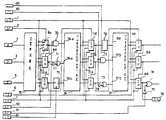
제3도에 비동기 순차회로를 대상으로한 종래의 스캔패스방식의 테스트회로예를 표시한다.3 shows an example of a conventional scan path type test circuit for an asynchronous sequential circuit.
도면에 있어서 참조번호 35는 조합회로의 블록, 참조번호 36,37은 순차회로를 포함한 비동기회로블록, 참조번호 8∼16은 각 회로블록간에 설치된 스캔레지스터, 참조번호 26∼34는 대응하는 회로블록의 출력과 스캔레지스터의 출력중에서 어느 것인가를 선택하여 출력하는 데이터셀렉터이다.In the drawing,
상기 스캔레지스터의 데이터입력단자(D)에는 및 데이터셀렉터의 데이터입력단자(D)에는 각 회로블록의 출력신호가 직집입력되고도 데이터셀렉터의 테스트데이터입력단자(TD)에는 대응하는 스캔레지스터의 출력단자(Q)가 접속되었다.The output signal of each circuit block is directly input to the data input terminal D of the scan register and the data input terminal D of the data selector, but the corresponding scan register is output to the test data input terminal TD of the data selector. Terminal Q is connected.
또한 1은 테스트모드선택단자이고, 당해 단자(1)는 스캔레지스터와 데이터셀렉터의 각 모드선택단자(MS)에 접속되어 있다.1 is a test mode selection terminal, and the
2는 스캔인 단자(scan-in terminal), 38은 스캔아우트단자(scan-out terminal)이다.2 is a scan-in terminal and 38 is a scan-out terminal.
스캔인단자(2)는 스캔레지스터(8)의 스캔인단자(S1)에 접속되고 스캔레지스터(8)의 출력단자(Q)는 스캔레지스터(9)의 스탠인단자(S1)에 접속되어 있고 이와 같이 각 스탠레지스터의 출력단자(Q)는 마음의 스캔레지스터의 스캔인단자(S1)에 순차 접속되며, 결과적으로 스캔인단자(2)와 스캔아우트단자(38)의 사이에서 시프트레지스터패스(shift register pass)가 형성되어 있다.The scan in
3∼5는 통상의 데이터입력단자, 6은 스캔클럭입력단자이고 당해단자(6)는 스캔레지스터의 클럭입력단자(T)에 접속되었다. 제4도는 제3도에 표시한 스캔레지스터의 일예이고, MS 모드선택단자, D는 데이터입력단자, S1는 스캔인단자 T는 클럭입력단자이다.3 to 5 are normal data input terminals, 6 are scan clock input terminals, and the
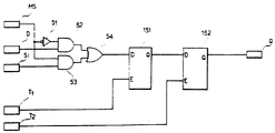
또한 51은 인버터, 52,53은 2입력앤드게이트, 54는 2입력오어게이트, 55는 에지트리거방식 D타입 플립플롭(이하, D-FF라고 한다.), 그리고 Q는 데이터출력단자이다.51 is an inverter, 52 and 53 are two input and gates, 54 is a two input or gate, 55 is an edge trigger type D flip-flop (hereinafter referred to as D-FF), and Q is a data output terminal.
제5도는 상기 제3도에서 도시한 데이터셀렉터의 일예이고 MS는 모드선택단자, TD는 테스트데이터입력단자, D는 데이터입력단자, 60은 인버터, 61,62는 2입력엔드게이트 63은 2입력오어게이트, 그리고 Y는 출력단자이다.FIG. 5 is an example of the data selector shown in FIG. 3, where MS is a mode selection terminal, TD is a test data input terminal, D is a data input terminal, 60 is an inverter, 61 is
다음은 동작에 대하여 설명한다.The following describes the operation.
우선 통상 동작시에 대하여 설명하면 이 경우는 레스트모드선택단자(1)(MS)에 "H"가 인가되고 스캔클럭단자(6)(TS 또는 T)는 "L"에 고정된다.First, the normal operation will be described. In this case, "H" is applied to the rest mode selection terminal 1 (MS) and the scan clock terminal 6 (TS or T) is fixed to "L".
결과로서 각 데이터셀렉터를 통하여 대응하는 회로블록간의 입출력단자가 집적 접속되는 것이 된다.As a result, the input / output terminals between the corresponding circuit blocks are integrated through each data selector.
이것을 제5도에 의하여 설명하면 데이터셀렉터는 모드선택단자(MS)에 "H"가 부여되면 데이터입력단자(D)에서의 데이터를 엔드게이트(62) 및 오어게이트(63)을 통하여 출력단자(Y)에 출력한다.Referring to FIG. 5, when "H" is applied to the mode selection terminal MS, the data selector outputs the data at the data input terminal D through the
회로블록의 출력은 이 테이터셀렉터의 데이터입력단자(D)에 직접접속되는 것이 있으므로 대응하는 각 회로블록간의 입출력단자가 직접 접속되는 것이 된다.Since the output of the circuit block is directly connected to the data input terminal D of this data selector, the input / output terminals between the corresponding circuit blocks are directly connected.
한편, 테스트동작시에는 다음과 같이 스캔모드와 테스트모드를 순차 반복하여 실행하고 각 회로블록의 테스트를 실시한다.On the other hand, during the test operation, the scan mode and the test mode are repeatedly executed in sequence as follows to test each circuit block.
1. 스캔모드1. Scan Mode
ⓐ 레스트모드선택단자(1)에 "H"를 인가하여 스캔모드로 한다. 이것에 의하여 스탠레지스터에는 스캔인단자(S1)에서의 입력데이터가 선택되고 데이터셀렉터에서는 데이터입력단자(D)에서의 입력데이터가 유효하게 된다.Ⓐ A scan mode is applied by applying “H” to the rest
ⓑ 더우기 스캔인단자(2)에서 각 스캔레지스터에 설정하는 테스트데이터를 스캔클럭단자(6)에 인가하는 클럭에 동기시켜서 순차 스캔인시킨다.Furthermore, the test data set in each scan register in the scan in
ⓒ 이와 동시에 스캔아우트단자(38)에서는 전회의 레스트시에 각 회로블록에 입력된 출력데이터가 순창적으로 스캔아우트(scan out)된다.At the same time, the scan-out
이 동작을 제4도 및 제5도에 의하여 설명하면 우선 스캔레지스터에 있어서도 모드선택단자(MS)에 "H"가 부여되면 스캔인단자(S1)에서의 데이터가 앤드게이트(53), 오어게이트(54)를 통하여 클럭단자(T)에 인가되는 클럭에 동기하여 D-FF(55)에 유지되고 또한 이것과 동시에 유지되어 있던 데이터가 출력단자(Q)에서 출력된다.4 and 5, when " H " is applied to the mode selection terminal MS in the scan register, the data at the scan in terminal S1 is transferred to the
더우기 이때 데이터셀렉터의 모드선택단자(MS)에도 "H"가 부여되어 있고 따라서, 출력단자(Y)에는 데이터 입력단자(D)에서의 데이터가 출력된다.Further, at this time, "H" is also given to the mode selector terminal MS of the data selector, so that data at the data input terminal D is output to the output terminal Y. FIG.
2. 테스트모드2. Test Mode
ⓐ 소망의 데이터가 각 스캔레지스터에 설정된 다음 테스트모드선택단자(1)에 "L"를 인가하여 테스트모드로 한다.Ⓐ After the desired data is set in each scan register, "L" is applied to the test mode selection terminal (1) to enter the test mode.
ⓑ 이것에 의하여 스캔레지스터의 출력데이터가 데이터셀렉터의 테스트입력단자(TD)를 경유하여 각 회로블록에 인가된다.By this, the output data of the scan register is applied to each circuit block via the test input terminal (TD) of the data selector.
ⓒ 동시에 데이터입력단자(3)∼(5)에 소망의 테스트데이터를 인가한다.Ⓒ At the same time, the desired test data is applied to the data input terminals (3) to (5).
ⓓ 다음에 회로블록의 동작이 완료된 시점에서 스캔클럭입력단자(6)에 클럭을 인가한다.Next, a clock is applied to the scan
이에 의하여 각 회로블록의 출력신호가 대응하는 스캔레지스터의 데이터 입력단자(D)를 통하여 스캔레지스터내의 D-FF에 유지된다.As a result, the output signal of each circuit block is held in the D-FF in the scan register through the data input terminal D of the corresponding scan register.
이들의 동작을 제4도 및 제5도에 의하여 설명하면 우선 스캔레지스터에서는 모드선택단자(MS)에 "L"가 부여되면 데이터입력단자(D)에서의 데이터가 앤드게이트(52), 오어게이트(54)를 통하여 클럭입력단자(T)에 인가되는 클럭에 동기하여 D-FF(55)에서 유지된다, 또한 이때 데이터셀렉터의 모드선택단자(MS)에도 "L"가 부여되므로 그 출력단자(Y)에는 테스트데이터입력단자(TD)에서의 데이터가 앤드게이트(61),오어게이트(63)를 통하여 출력된다.4 and 5, first, in the scan register, when "L" is applied to the mode selection terminal MS, the data at the data input terminal D is transferred to the AND
이와 같이하여 각 회로블록(35)∼(37)의 테스트를 실행할 수 있지만, 본 회로에서는 스캔의 동작중에 있어서는 데이터셀렉터가 각 회로블록의 출력데이터를 선택하고 있고 이것에 의하여 스캔동작중에 스캔레지스터의 출력값이 순차로 변하여도 순서회로를 포함한 회로블록(36)의 상태가 변화하지 않게 되어 있다.In this way, the tests of the respective circuit blocks 35 to 37 can be executed. However, in this circuit, the data selector selects the output data of each circuit block during the scan operation. Even if the output value changes sequentially, the state of the
따라서 이예에서와 같이 스캔패스에 포위된 회로블록이 비동기순차회로라 할지라도 스캔테스트가 가능하게 되었다.Thus, even in this example, even if the circuit block surrounded by the scan path is an asynchronous sequence circuit, scan test is possible.
종래의 장치는 상기와 같이 구성되어 있으므로 비동기 순서회로를 포함한 블록에 대하여서도 스캔테스트를 할 수가 있다.Since the conventional apparatus is configured as described above, the scan test can also be performed on the block including the asynchronous sequence circuit.
그러나 일반적으로는 테스트모드에서 스캔모드로 전환할때에 순서회로에 부여되는 데이터는 시리얼로 입력된 신호값에 인접하는 회로블록의 출력신호값으로 변화되어 버린다.In general, however, when the test mode is switched from the scan mode, the data given to the sequential circuit is changed to the output signal value of the circuit block adjacent to the serial signal value.
이 때문에 대상으로하는 비동기순차회로의 상태가 변화하지 않게 입력을 설정하는 것이 곤란하여 많은 경우 스캔테스트를 유효하게 실시할 수가 없다는 문제가 있었다.For this reason, it is difficult to set the input so that the state of the target asynchronous sequential circuit does not change, and in many cases, there is a problem that the scan test cannot be effectively performed.
본 발명은 상기와 같은 문제점을 해결하기 위하여 창안된 것으로서 비동기 순차회로를 포함한 회로블록을 포함하여 적은 제어신호입력핀으로 용이하게 스캔테스트가 가능한 반도체집적회로장치를 얻고자하는 것이다.SUMMARY OF THE INVENTION The present invention has been made to solve the above problems, and is to obtain a semiconductor integrated circuit device that can be easily scanned and tested with a small number of control signal input pins, including a circuit block including an asynchronous sequential circuit.
본 발명에 의한 반도체집적회로장치는 피(被)테스트회로 블록의 사이에서 통상의 동작시는 입출력단자 사이를 도통(through) 상태로하여 입력데이터를 그대로 출력하고, 테스트동작시는 입력데이터를 유지출력하기 위해 테스트되는 회로블럭들 사이에 제공된 스캔레지스터와 이 스캔레지스터의 출력단자에 접속되며, 통상 동작시 및 테스트모드에서의 테스트 동작시 게이트제어의 입력으로 테스트데이타의 출력을 위한 소정의 고정값을 출력하는 게이트회로를 포함한다.The semiconductor integrated circuit device according to the present invention outputs the input data as it is while the normal operation is performed between the I / O terminals during normal operation between the test circuit blocks, and maintains the input data during the test operation. It is connected to the scan register provided between the circuit blocks being tested for output and the output terminal of the scan register, and a predetermined fixed value for the output of the test data as the input of the gate control during the normal operation and the test operation in the test mode. It includes a gate circuit for outputting.
테스트모드에 있어서는 상기 스캔레지스터의 출력데이타를 출력하고 그리고 테스트 동작시의 스캔모드에 있어서는 각각 제1의 고정데이터(당해 제1의 고정데이타라고 함은 반대논리값의 제2의 고정데이터 또는 전주기의 스캔레지스터의 출력데이터이다)를 출력하는 제1, 제2의 게이트회로 및 래치회로와 상기 제1 또는 제2의 게이트회로의 제어입력에 접속된 부정회로를 설치하여 적어도 동일단의 상기 제1 또는 제2의 게이트회로의 제어입력과 부정회로의 입력과를 동일의 제어신호에 접속한다.In the test mode, the output data of the scan register is output, and in the scan mode during the test operation, the first fixed data (the first fixed data is referred to as the second fixed data of the opposite logic value or the entire period, respectively). First and second gate circuits and latch circuits for outputting the scan registers of the scan registers and negative circuits connected to the control inputs of the first or second gate circuits. Alternatively, the control input of the second gate circuit and the input of the negative circuit are connected to the same control signal.
상기 테스트 동작시의 스캔모드에 있어서는 소정의 고정치를 출력하는 게이트회로를 설정하여 테스트데이터의 출력을 게이트제어입력에 의하여 콘트롤할 수 있게 하고 또한 소정의 고정치를 출력하는 게이트회로 및 스캔 동작전의 스캔레지스터의 출력데이터를 출력하는 래치회로를 설정하여 테스트데이터의 출력을 제어입력에 의하여 콘트롤할 수 있게 한 것이다.In the scan mode during the test operation, a gate circuit for outputting a predetermined fixed value is set so that the output of the test data can be controlled by the gate control input, and the gate circuit for outputting the predetermined fixed value and before the scan operation. By setting a latch circuit that outputs the scan register output data, the output of the test data can be controlled by the control input.
이 발명에 있어서는 스캔레지스터의 출력에 삽입된 게이트회로에 의하여 피 테스트회로블록에 대해 따른 회로블록의 출력에 관계없이 스캔시에는 소정의 고정치를 그리고 테스트시는 소정의 타이밍으로서의 데이터를 인가하는 것이 가능하게 되어서 테스트동작시의 모드전환하는데 있어 피 테스트회로블록에 주어지는 데이터가 변경되는 것이 방지된다.In the present invention, the gate circuit inserted into the scan register outputs a fixed value at the time of scanning and data at a predetermined timing during the test regardless of the output of the circuit block with respect to the circuit block under test. This makes it possible to prevent the data given to the circuit under test from changing in mode switching during the test operation.
또, 스캔모드에 있어서 피 테스트회로블록의 입력을 스캔레지스터의 출력에 삽입한 게이트회로에 의하여 소정의 값을 고정할 수 있고, 또 래치회로에 의하여 전주기의 테스트데이터로 유지된다.Further, in the scan mode, a predetermined value can be fixed by a gate circuit in which the input of the circuit under test is inserted into the output of the scan register, and held by the latch circuit as test data for the entire period.
이 때문에 피 테스트회로블록의 입력신호가 스캔중에 변환하는 것을 방지할 수가 있다.For this reason, it is possible to prevent the input signal of the circuit under test from being converted during scanning.
또, 테스트시에 양의 클럭신호와 그와 동일한 타이밍의 음의 신호를 한개의 제어로서 콘트롤할 수 있으며 또한 테스트모드로부터 스캔모드로의 전환시에 테스트데이터가 변화하는 일이 없으므로 적은 핀수로서 비동기순서회로를 포함하는 회로블록을 용이하게 스캔테스트할 수 있다.In addition, a positive clock signal and a negative signal at the same timing can be controlled as a control during the test, and test data does not change when switching from the test mode to the scan mode. The circuit block including the sequential circuit can be easily scanned.
이하, 본 발명의 실시예를 도면에 의하여 설명한다.Best Mode for Carrying Out the Invention Embodiments of the present invention will now be described with reference to the drawings.
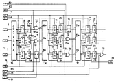
제1a도에 있어서 제3도와 동일부호는 동일 또는 상당부분을 표시하고 35∼37은 피 테스트회로블록이고 이들의 접속부분에 본 발명의 일실시예에 의한 테스트회로가 연결되어 있다.In FIG. 1A, the same reference numerals as those in FIG. 3 denote the same or corresponding parts, and 35 to 37 are the circuit blocks to be tested, and test circuits according to one embodiment of the present invention are connected to these connection parts.
8a~16a는 스캔레지스터이고 상세한 설명은 후술한다.8a to 16a are scan registers, which will be described later.
75,76는 각각 스캔레지스터(10a,11a)의 출력단자에 접속되어 도통(through)기능을 가진 래치이고, 이 래치(75),(76)은 단자(3)입력이 "H"라면 단자(D)입력데이터를 그대로 출력단자(Q)에 전달하고, "L"가 되면 래치한 내용을 출력단자(Q)에 유지출력하는 것이다.75 and 76 are latches having a through function connected to the output terminals of the scan registers 10a and 11a, respectively, and the
70,72는 스캔레지스터와 회로블록사이에 설치된 앤드게이트 71,73,74는 동일하게 스캔레지스터와 회로블록사이에 설치된 오어게이트, 77,78,79는 오아게이트의 제어입력에 접속된 인버터이다.70, 72 is an AND
또한, 81,82는 래치제어입력단자, 80,90,91은 게이트제어입력단자, 36a∼36c, 37a∼37c는 이 테스트회로블록의 입력이다.In addition, 81 and 82 are latch control input terminals, 80 and 90 and 91 are gate control input terminals, and 36a to 36c and 37a to 37c are inputs of this test circuit block.
여기에서 본 실시예에 의한 회로블록(36),(37)에 있어서 그 입력(36a),(37a)는 액티브(H)의 입력, 입력(36b),(37c)는 액티브(L)의 입력이고, 또한 입력(36c)(37c)는 입력 데이터가 H→L, L→H의 어느 방향으로 변화하여 내부상태가 변화하도록되는 입력으로 되어 있다.Here, in the circuit blocks 36 and 37 according to the present embodiment, the
또한 7은 변화하도록 되는 입력으로 되어 있다. 또한 7은 통상 동작과 테스트동작을 전환하기 위한 노멀모드입력단자이다.7 is an input to be changed. 7 is a normal mode input terminal for switching between normal operation and test operation.
또 입력(36c),(37c)는 다읍 입력에 비액티브상태의 신호가 입력되어 있으면 해당 입력(36a),(37a)에의 신호가 변화하여도 피 테스트 회로블록의 상태를 변화시키지 않는 입력으로 되어 있다.The
또 본 실시예에 있어서, 스캔레지스터는 종래와는 상이하고 제6도에 도시한 바와 같이 구성되어 있다.In the present embodiment, the scan register is different from the conventional one and is configured as shown in FIG.
즉, 제6도에 있어서 56은 인버터, 57,58은 앤드게이트 59는 오어게이트이며 다른 구성은 제4도에 표시된 것과 동일하다.That is, in FIG. 6, 56 is an inverter, 57, 58 are AND
이와 같이 구성된 스캔레지스터는 노멀모드신호(NM)가 "H"라면 입력단자(D)의 데이터를 출력단자(Q)에 그대로 전달하고 역으로 "L"이면 제4도의 종래의 레지스터와 동일기능이 되는 것이다.The scan register configured as described above transfers the data of the input terminal D to the output terminal Q as it is when the normal mode signal NM is "H", and the same function as the conventional register of FIG. Will be.
다음은 동작에 대하여 설명한다.The following describes the operation.
우선 통상 동작시에 대하여 설명한다.First, normal operation will be described.
통상 동작시에는 노멀모드입력(7)에 "H", 래치제어입력(81),(82)에 "H", 게이트제어입력(80),(90),(91)에 "H"를 오어게이트에 접속되어 있는 제어입력에 "L"를 인가한다. 이것에 의하여 모든 스캔레지스터는 D입력에서 Q출력까지 신호가 그대로 전달됨과 동시에 래치(75),(76) 및 게이트(70)∼(74)는 입력을 그대로 출력까지 전달한다.In normal operation, " H " for the
그 때문에 회로블록간의 데이터는 테스트회로에 영향을 미치지 않고 그대로 전달되어 소망의 통상동작을 할 수가 있다.Therefore, the data between the circuit blocks can be transferred as it is without affecting the test circuit and can perform desired normal operation.
다음에서 테스트동작 즉 노멀모드입력(7)을 "L"로 한 경우에 대하여 기술한다.The following describes the test operation, that is, the case where the
이 경우에 있어서 테스트모드선택단자(1)의 신호에 의하여 스캔모드와 테스트모드의 전환을 한다.In this case, the scan mode and the test mode are switched by the signal of the test
그리고 이 2개의 모드를 반복하므로서 피테스트회로의 테스트를 한다.The circuit under test is tested by repeating these two modes.
1. 스캔모드1. Scan Mode
테스트모드선택단자(1)을 "H"로 하므로서, 스캔모드가 된다.The scan mode is set by setting the test
이 모드에서는 스캔클럭입력단자(6)에 클럭을 부여하므로서 스캔패스를 구성하는 스캔레지스터에 테스트데이터를 스캔인(scan in), 스캔아우트(scan out)할 수가 있다.In this mode, the clock is input to the scan
이 동작의 예를 제2a도에 표시한다.An example of this operation is shown in FIG. 2A.
도면에 있어서 입력(1)을 "H"로 한 경우가 스캔모드이다.In the figure, the case where the
본 실시예에 있어서는 스캔동작시에 스캔레지스터의 출력단자(Q)에 스캔데이터가 출력되기 때문에 이 데이터에 사용한 신호의 변화가 생긴다.In this embodiment, since scan data is output to the output terminal Q of the scan register during the scan operation, a change in the signal used for this data occurs.
그러나, 스캔모드에 있어서 래치제어입력(81),(82)를 "L"로 하여두면 피테스트회로로의 입력(36c),(37a)는 스캔동작전의 데이터를 취할 수 있다.However, in the scan mode, when the
또한 게이트제어입력(80),(90)를 전부 "L"로 하여두면 입력(36a),(37b)는 "L", 입력(36b),(37c)는 "H"로 고정된다.If the
이와 같이 스캔모드시에 있어서 피테스트회로블록의 입력을 고정할 수 있기 때문에 회로블록의 상태를 유지할 수 있다.In this manner, since the input of the circuit under test can be fixed in the scan mode, the state of the circuit block can be maintained.
제2b도에서는 신호변화를 표시하기 위하여 70a∼73a는 스캔중의 부정치를 취하고 또한 스캔클럭에 동기하여 변화할 수 있음을 표시하고 있다.In FIG. 2B, in order to indicate a signal change, 70a to 73a indicate that a negative value during scanning can be taken and can be changed in synchronization with the scan clock.
그러나, 스캔모드에 있어서 게이트제어입력 (80),(90),(91)을 각각 "L", "H", "H"로 하여두고 각 게이트(70)∼(74)에 의하여 스캔레지스터이 출력변화는 피 테스트회로블록의 입력에는 전달되지 않고 소정의 값으로 고정된다.However, in the scan mode, the
즉, 피 테스트회로블록의 입력(36a),(36b),(37b),(37c)은 각가 "L", "H", "L", "H"로 고정하고, 이 값은 각 입력에 대하여 비 액티브한 값이므로 회로블록을 유지상태로 유지할 수가 있다.That is, the
더우기 전술한 바와 같이 입력(36c),(37a)은 타입력에 비 액티브한 값이 입력되어 있는한 입력되는 데이터의 값에 불구하고 피 테스트회로블록의 상태를 유지하게하는 액티브값이 입력되어 있으므로 회로블록을 유지상태로 유지할 수가 있다.Furthermore, as described above, the
2. 테스트모드2. Test Mode
테스트모드시는 테스트모드 선택단자(1)를 "L"로 한다.In the test mode, the test
이 모드에서는 스캔레지스터의 내용을 이 테스트회로 블록에 입력하고 그후 피 테스트회로블록의 출력을 스캔레지스터로 입력하는 동작을 한다.In this mode, the contents of the scan register are input to the test circuit block, and then the output of the test circuit block to the test register is input.
이 동작의 예를 제2a도에 표시한다.An example of this operation is shown in FIG. 2A.
동 도면에 있어서 입력(1)를 "L"로 한 경우가 테스트모드이다. 여기서 이 테스트모드에 있어서 제2a도에 표시한 바와 같이 입력(36a),(36b),(36b)에는 펄스가 출력되고 입력(37c)에는 출력되지 않는다고 하면 스캔레지스터(8a),(9a),(12a),(13a)의 출력데이터는 각각 "H", "L", "H", "H"이다.In the figure, the case where the
또 스캔레지스터(10a), (11a)는 각각"H","L"를 출력하고 있는 것으로 한다.The scan registers 10a and 11a output "H" and "L", respectively.
이들 테스트데이터는 래치회로(75),(76) 및 게이트(70)∼(73)을 스루상태로 하는 것에 의하여 테스트회로블록에 부여할 수가 있다.These test data can be provided to the test circuit block by putting the
제2도에 있어서 래치(75),(76)의 출력은 각각 래치제어신호(81e),(82e)의 상승에 동기하여 출력되며, 각각 신호(36ce),(36ae)와 같이 변화하고 이들 데이터가 각 래치(75),(76)에 유지된다.In Fig. 2, the outputs of the
또한 게이트(70)∼(73)의 출력은 각각 펄스(90p), (90p), (80p), (80p)의 기간에만 출력되므로 각각 파형(36ap), (36bp), (37bp), (37ce)과 같이 된다.In addition, the outputs of the
이와 같이하여 피 테스트회로블록에 테스트데이터를 부여한후에 회로블록에서 출력되는 테스트결과를 스캔클럭입력단자(6)에 펄스(6p)를 부여하여 스캔레지스터로 입력한다.In this manner, after the test data is applied to the circuit block under test, the test result output from the circuit block is applied to the scan
테스트결과 데이터는 다음의 스캔동작시에 순차 스캔아우트 된다.The test result data is sequentially scanned out during the next scan operation.
이와 같은 본 실시예에서는 스캔레지스터의 출력에 래치 내지 앤드게이트 또는 오어게이트를 접속하였으므로 그 제어입력을 콘트롤하는 것에 의하여 스캔모드에 있어서 피 테스트회로의 동작을 정지할 수 있고 더욱이 임의의 타이밍의 "H"또는 "L"이 테스트펄스를 피 테스트회로에 인가할 수가 있다.In the present embodiment as described above, since the latch, the AND gate, or the OR gate is connected to the output of the scan register, the operation of the circuit under test can be stopped in the scan mode by controlling the control input, and further, the " H " "Or" L "may apply a test pulse to the circuit under test.
또한 각 회로블록의 테스트데이터는 스캔데이터에서만 부여할 수가 있기 때문에 타의 회로블록의 출력데이터의 값을 고려하지 않고 테스트데이터를 생성할 수 있어 용이하게 스캔테스트를 실시할 수 있다.In addition, since the test data of each circuit block can be given only in the scan data, the test data can be generated without considering the value of the output data of the other circuit block, so that the scan test can be easily performed.
또한 통상 앤드(AND)회로와 오어(OR)회로를 설정했을 경우 그 제어입력에서는 각각 별도의 제어신호가 접속되는 것이지만 본 실시예에서는 오어회로의 제어입력단자에 인버터를 접속하고 있으므로 양의 신호와 그것과 동일타이밍의 음의 신호를 한개의 제어입력으로 콘트롤할 수가 있어 집적회로의 핀수를 감소할 수가있다.In addition, when the AND circuit and the OR circuit are normally set, separate control signals are connected to the control inputs of the control input, but in this embodiment, the inverter is connected to the control input terminal of the OR circuit. The same timing can be controlled by one control input, reducing the number of pins in the integrated circuit.
더욱이 상기 실시예에서는 오어게이트의 제어입력단자에 인버터를 설치한 경우에 대하여 설명하였지만 앤드게이트(70),(72)의 제어입력단자와 인버터를 설치하여도 되고 상기 실시예와 동일한 효과를 발휘한다.Moreover, in the above embodiment, the case where the inverter is provided in the control input terminal of the or gate has been described, but the control input terminal and the inverter of the AND
또한 상기 실시예에서는 동일단의 앤드회로와 오어회로의 제어입력을 접속한 경우에 대하여 설명하였지만, 가령 회로블록(36),(37)의 입력타이밍이 동일하다면 각 게이트회로(70)∼(73)의 제어입력 모두를 동일제어신호에 접속하는 것도 가능하다.In the above embodiment, the case where the control inputs of the AND circuit and the OR circuit of the same stage are connected has been described. For example, if the input timings of the circuit blocks 36 and 37 are the same, the
또한 이 동작의 예를 제2b도에 표시한다.An example of this operation is also shown in FIG. 2B.
동 도면에 있어서 입력(1)을 "L"로 한 경우가 테스트모드이다.In this figure, the case where the
이 경우는 게이트제어입력(80)이 "H"인 경우는 게이트제어입력(80)을 "H", 90.91을 "L"로 하므로서 스캔레지스트내의 테스트데이터를 각 게이트회로를 통하여 또는 직접으로 피 테스트회로블록에 입력할 수가 있다.In this case, when the
제2b도에 표시한 바와 같이 테스트모드에서는 앤드게이트(70)이 스캔레지스터(8a)에서 "H"가 입력되어 있으므로 제어입력(80)에 "H"펄스(80p)가 부여되면 당해 80p와 동일파형의 "H"p펄스(36ap)를 출력한다. 또 동일하게 오어게이트(71)는 그 한편 입력(71a)(스캔레지스터(9a)의 출력)에 "L"가 입력되어 있기 때문에 제어입력(90)에 "L"펄스(90p)가 부여되면 당해 펄스(90bp)와 동일파형의 "L"펄스(36p)를 출력한다.As shown in FIG. 2B, in the test mode, the AND
한편 앤드게이트(72) 및 오어게이트(73)에는 제2b도에 표시한 바와 같이 스캔레지스터에서 각각 "L", "H"가 부여되고 있기 때문에 스캔모드시와 동일하게 되어 게이트제어입력이 각각 펄스(80p), (90p)와 같은 신호를 입력하여도 상기와 같은 펄스파형이 출력되는 것은 아니다.On the other hand, since the "L" and "H" are respectively given to the AND
이와 같이하여 피 테스트회로블록에 테스트데이터를 부여하여 출력되는 테스트결과를 클럭입력단자(6)에 펄스(sp)를 부여하여 스캔레지스터에 조입하여 1주기분의 테스트를 한다.In this way, test data is applied to the test circuit block under test and pulses (sp) are applied to the
상기와 같은 구성으로서는 게이트회로를 통하여 출력되는 테스트데이터는 스캔레지스터의 값에 의하여 출력값이 결정되며 게이트제어입력에 의하여 타이밍이 결정되어 있다고 해석된다.In the above configuration, the test data output through the gate circuit is interpreted that the output value is determined by the value of the scan register and the timing is determined by the gate control input.
이 때문에 동일 타이밍으로 테스트펄스를 발생하는 게이트회로(70), (72), (73), (74)는 게이트제어단자를 공통으로 접촉할 수 있다.For this reason, the
이와 같은 본 실시예에서는 스캔레지스터의 출력에 앤드게이트 또는 오어게이트를 접속하였으므로 그 제어입력을 콘트롤하므로서 스캔모드에 있어서 피 테스트회로의 동작을 정지할 수가 있고 더우기 임의의 타이밍의 "H" 또는 "L"의 테스트펄스데이터를 피 테스트회로에 인가할 수가 있다.In this embodiment, since the AND gate or the OR gate is connected to the output of the scan register, the control input can be controlled to stop the operation of the circuit under test in the scan mode. Furthermore, "H" or "L" at an arbitrary timing can be stopped. Test pulse data can be applied to the circuit under test.
또한 각 회로블록의 테스트데이터는 스캔데이터에서만 부여되기 때문에 타 회로블록에 영향되지 않고 테스트데이터를 생성할 수 있고 용이하게 스캔테스트를 실시할 수 있다.In addition, since test data of each circuit block is given only to scan data, test data can be generated without being influenced by other circuit blocks, and scan test can be easily performed.
더우기 상기 실시예에서는 스캔레지스터를 제6도에 표시한 구성으로 하였지만 이 스캔레지스터의 구성은 이것에 한정되는 것은 아니고 예를 들면 제8a도에 도시한 구성으로 하여도 된다.Furthermore, in the above embodiment, the scan register is shown in Fig. 6, but the configuration of the scan register is not limited to this and may be, for example, shown in Fig. 8A.
제8a도에 있어서 제6도와 동일부호 또는 동일부분을 표시하고 151,152는 E입력을 "H"로 하면 입력(D)에서 출력(Q) 데이타가 그대로 전달하고, E입력이 "L"가 되면 입력(D)를 래치하고 출력(Q)에 유지데이터를 출력하는 래치이다.In FIG. 8A, the same reference numerals or the same parts as those of FIG. 6 are shown. In the case of 151 and 152, when the E input is "H", the output (Q) data is transferred from the input (D) as it is. A latch for latching (D) and outputting maintenance data to the output (Q).
이 스캔레지스터를 사용한 테스트방법을 설명하면 우선 통상 동작시는 단자(MS)를 "L", 단자(T1), (T2)를 "H"로 한다.The test method using this scan register will be described. First, in the normal operation, the terminal MS is "L", and the terminals T1 and T2 are "H".
스캔모드에서는 단자(MS)에 "H"를 단자(T1),(T2)를 2상 클럭을 인가하고 테스트모드에서는 단자(MS)에 "L"를 단자(T2)에 "L"를 인가한다.In the scan mode, "H" is applied to the terminal MS and the two-phase clock is applied to the terminals T1 and T2. In the test mode, "L" is applied to the terminal MS and "L" is applied to the terminal T2. .
더우기 게이트신호는 상기에서 표시한 바와 같이 된다.Furthermore, the gate signal is as indicated above.
상기 설명에서 명백한 바와 같이 본 발명의 스캔레지스터는 다음의 기능을 가지고 있으면 되는 것이다.As apparent from the above description, the scan register of the present invention should have the following functions.
1. 데이터입력을 그대로 전파하는 통상 동작기능.1. Normal operation function to propagate data input as it is.
2. 스캔인단자에서 스캔아우트단자까지 스캔레지스터를 직렬접속하여 스캔패스를 구성하고 데이터를 스캔동작시키는 스캔기능, 이경우 스캔레지스터의 출력은 변화하여도 되고 하지 않아도 된다.2. Scan function that connects scan registers from scan-in terminal to scan-out terminal in series to configure scan path and scan data. In this case, output of scan register may or may not be changed.
3. 스캔인된 데이터를 유지하고 출려단자에 유지데이터를 출력하는 기능.3. The function to keep the scanned data and output the maintenance data to the terminal.
4. 3의 기능과 동시에 피 테스트회로블록에서의 출력을 조입하는 기능.4. Simultaneously with
더우기 본 발명의 기본원리를 종래회로에 적용하여 제7a도에 표시한 바와 같은 회로장치를 구성할 수가 있다.Furthermore, by applying the basic principle of the present invention to a conventional circuit, a circuit device as shown in Fig. 7A can be constructed.
즉, 제7a도는 종래에의 테스트회로의 출력측에 게이트회로를 첨가한 것이다.That is, in FIG. 7A, a gate circuit is added to the output side of a conventional test circuit.
이 제7a도에 표시한 회로의 동작에 대하여 설명하면 우선 통상 동작시는 모드선택단자(1) 제어입력(8)을 "H", 제어입력(90),(91)을 "L"로 하고 스캔모드에서는 선택단자(1), 제어입력(90),(91)를 "H"제어입력(80)을 "L"로 하고 테스트모드에서는 선택단자(1)을 "L", 제어입력(80),(90),(91)에 각각 소망의 타이밍의 "H"펄스 "L"펄스를 인가한다.Referring to the operation of the circuit shown in FIG. 7A, first, in the normal operation, the
이러한 구성이 되는 회로장치에 있어서도 상기 실시예와 동일한 효과를 나타낸다.Also in a circuit device having such a configuration, the same effects as in the above embodiment are obtained.
여기에서 제2c도에 도시한 테스트모드에서는 스캔레지스터(8a), (9a), (10a), (11a), (12a), (13a)는 각기 "H", "L", "H", "H", "L", "H"를 출력하고 있다고 한다.In the test mode shown in FIG. 2C, the scan registers 8a, 9a, 10a, 11a, 12a, and 13a are respectively "H", "L", "H", "H", "L", and "H" are reported.
이들의 테스트데이터는 래치(76),(76) 및 게이트(70)∼(73)을 스루상태로 하는 것에 의하여 피 테스트회로블록에 부여할 수가 있다.These test data can be provided to the circuit under test by putting the
제2c도에 있어서 래치(75),(76)의 출력은 각기 래치제어신호(81a), (82e)의 상승에 동기하여 출력되고 각기 신호(36ce), (36ae)와 같이 변화하고 이 데이터가 당해 래치(75),(76)에 유지된다.In Fig. 2C, the outputs of the
또한 게이트(70)∼(73)의 출력은 각기 펄스(80p), (90p), (80p), (91p)의 기간만큼 출력되므로 각기 파형(36ap), (36bp), (37bp), (37cp)와 같이 된다.In addition, the outputs of the
이와 같이 하여 피 테스트회로블록에 테스트데이터를 부여한 후에, 회로블록에서 출력되는 테스트 결과를 스캔클럭입력단자(6)에 펄스(6p)를 부여하여 스캔레지스터로 입력한다. 이 테스트 결과 데이터는 다음 스캔 동작시에 순차 스캔아우트 된다.After the test data is applied to the circuit block under test in this manner, the test result output from the circuit block is applied to the scan
상기한 바와 같은 구성에서는 래치 내지 게이트회로를 통하여 출력되는 테스트데이터는 스캔레지스터의 값에 의하여 출력치가 결정되고 게이트제어입력에 의하여 동일 타이밍으로 테스트펄스를 발생하는 게이트회로(70), (72), (73), (74)는 게이트제어단자를 공통으로 접속할 수 있다.In the above-described configuration, the test data output through the latch or gate circuit has an output value determined by the value of the scan register, and the
또 게이트출력신호펄스의 개시타이밍과 래치출력신호의 변화타이밍이 동일하고 게이트회로와 래치회로의 스루기능이 동일한 제어방법이라면 이들을 공통으로 접속할 수 있다.In addition, as long as the start timing of the gate output signal pulse and the change timing of the latch output signal are the same and the through functions of the gate circuit and the latch circuit are the same, they can be connected in common.
이와 같은 본 실시예에서는 스캔레지스터의 출력에 래치 내지 앤드게이트 또는 오어게이트를 접속하였으므로 그 제어입력을 콘트롤하는 것에 의하여 스캔모드에 있어서 테스트회로의 동작을 정지할 수가 있고 더우기 테스트시에 임의의 지연을 가진 테스트데이터 또는 임의의 지연과 폭을 가진 테스트펄스를 인가할 수가 있다.In the present embodiment as described above, since the latch or the end gate or the or gate is connected to the output of the scan register, the control input can be controlled to stop the operation of the test circuit in the scan mode. Excitation test data or test pulses with arbitrary delay and width can be applied.
또, 각 회로블록의 테스트데이터는 스캔데이터에서만 부여되기 때문에 타 회로블록에 영향되지 않고 테스트데이터를 생성할 수 있어 용이하게 스캔테스트를 실시할 수 있다. 더우기 상기 실시예에서는 스캔레지스터를 제6도에 표시한 구성으로 하였지만 이 스캔레지스터의 구성은 이것에 한정되는 것은 아니고 예를 들면 제8b도에 표시한 구성으로 하여도 된다. 제8b도에 있어서 100은 n-MOS의 트랜스퍼게이트 101∼104는 인버터이고 그중 인버터(102), (104)는 드리이브 능력이 매우 작은 것이다.In addition, since the test data of each circuit block is given only to the scan data, the test data can be generated without being influenced by other circuit blocks, so that the scan test can be easily performed. Furthermore, in the above embodiment, the scan register is shown in FIG. 6, but the configuration of the scan register is not limited to this and may be, for example, shown in FIG. 8B. In Fig. 8B, 100 is n-
이와 같이 구성된 스캔레지스터는 각 모드에 의하여 다음과 같이 동작한다.The scan register configured as described above operates as follows in each mode.
1. 통상모드1. Normal mode
입력 TP. TS2를 "H", TS1을 "L"로 한다. 그러면 입력(D)에서 출력(Q)까지 데이터가 그대로 전달한다.Input TP. TS2 is set to "H" and TS1 is set to "L". The data is then transferred as is from input (D) to output (Q).
2. 스캔모드2. Scan Mode
입력 TP를 "L"로 하고, TS1, TS2에 2상 클럭을 입력한다. 그러면 스캔인단자(S1)을 입력, 출력단자(Q)를 출력으로 하는 시프트레지스터의 1단이 형성된다.Set the input TP to "L" and input a two-phase clock to TS1 and TS2. Then, one stage of a shift register having the scan in terminal S1 as an input and the output terminal Q as an output is formed.
3. 테스트모드3. Test Mode
입력(TP), (TS1), (TS2)를 "L"로 한다. 스캔인된 테스트데이터는 인버터된(103),(104)로 된 래치에 유지되고 출력단자(Q)에 출력된다. 이후 스캔레지스터에 접속된 래치 또는 게이트에 소망의 펄스를 부여하므로서 피 테스트회로블록에 테스트데이터를 부여한다. 다시 이후에 입력(TP)에 "H"를 부여하여 테스트 결과를 인버터(101),(102)로된 래치로 입력된다.The inputs TP, TS1, and TS2 are set to "L". The scanned test data is held in the latches of the
상기 설명에서 명백한 바와 같이 본 발명의 스캔레지스터는 다음 기능을 가지고 있으면 된다.As apparent from the above description, the scan register of the present invention may have the following functions.
1. 데이터 입력을 그대로 전파하는 통상 동작기능.1. Normal operation function to propagate data input as it is.
2. 스캔인단자에서 스캔아우트단자까지 스캔레지스터를 직렬로 접속하여 스캔패스를 구성하고 데이터를 스캔동작시키는 스캔기능, 이 경우 스캔레지스터의 출력은 변화하여도 되고 하지 않아도 된다.2. A scan function that connects the scan registers serially from the scan-in terminal to the scan-out terminal to form a scan path and scans data. In this case, the output of the scan registers may or may not be changed.
3. 스캔인된 데이터를 유지하고 출력단자에 유지 데이터를 출력하는 기능.3. The function to keep the scanned data and output the maintenance data to the output terminal.
4. 3의 기능과 동시에 피 테스트회로블록에서의 출력을 조입하는 기능.4. Simultaneously with
또한 본 발명에 의하여 피 테스트회로블록에 부여되는 테스트데이터는 다음과 같이 된다.Further, the test data applied to the circuit under test by the present invention is as follows.
1. 래치출력1. Latch output
스캔시는 전회의 테스트데이터의 유지, 테스트시는 래치제어의 타이밍에 의하여 임의의 지연을 카진 테스트데이터.The test data is held at an arbitrary delay by the timing of the latch control during the test and the previous test data during the scan.
2. 앤드게이트출력2. End gate output
스캔시에는 "L"출력, 테스트시는 게이트제어펄스에 의해 임의 지연과 폭을 가진"H"의 테스트펄스."L" output during scan, "H" test pulse with arbitrary delay and width by gate control pulse during test.
또한 스캔인된 테스트데이터를 "L"에 의하면 테스트펄스는 출력되지 않는다.In addition, according to the scanned test data "L", the test pulse is not output.
3. 오아게이트출력3. Oagate output
스캔시는 "H"클럭, 테스트시는 게이트제어펄스에 의하여 임의의 지연과 폭을 가진 "L"의 테스트펄스 또한 스캔인된 테스트데이터를 "H"로 하면 테스트펄스는 출력되지 아니한다.If the "H" clock is used for the scan and the "L" test pulse has an arbitrary delay and width due to the gate control pulse during the test, and the scanned test data is set to "H", the test pulse is not output.
따라서 피 테스트회로블록의 테스트패턴에 상응하여 상기 3종류의 출력을 선정하면 비동기식 순서회로를 포함한 블록의 테스트를 용이하게 설시할 수가 있다.Therefore, if the above three types of outputs are selected according to the test pattern of the circuit under test, the test of the block including the asynchronous sequence circuit can be easily described.
또한 스캔시에 입력이 변화하여도 지장이 없는 신호는 래치를 통하지 않고 스캔레지스터출력을 그대로 접속하여도 된다.In addition, even if the input changes at the time of scanning, a signal that does not interfere may connect the scan register output as it is without passing through the latch.
더우기 본 발명의 기본원리를 종래회로에 적용하여 제7b도에 표시한 바와 같은 회로장치를 구성할 수 있다.Furthermore, by applying the basic principle of the present invention to a conventional circuit, a circuit device as shown in Fig. 7B can be constructed.
즉 이 제7b도는 종래에의 테스트회로의 출력에 래치 내지는 게이트회로를 첨가한 것이다.That is, in FIG. 7B, a latch or gate circuit is added to the output of the conventional test circuit.
이 제7b도의 실시예에 있어 동작을 다음에서 설명한다.The operation in the embodiment of FIG. 7B will be described next.
1.통상모드1. Normal mode
입력 (1), (80), (81), (82)를 "H", 90, 91를 "L"로 한다. 이것에 의하여 회로블록간의 신호는 테스트회로에 영향되지 않고 그대로 전달한다.The inputs (1), (80), (81), and (82) are set to "H", and 90 and 91 are set to "L". As a result, the signal between the circuit blocks is transmitted as it is without affecting the test circuit.
2.스캔모드2. Scan mode
입력(1), (90), (91)을 "H",80,81,82를 "L"로 하고 단자(6)에 스캔클럭을 스캔인단자(2)에 소망의 스캔데이터를 입력한다. 이 경우 스캔레지스터 사이에서 스캔동작을 하고 스캔아우트단자(38)에 스캔데이터가 출력됨과 동시에 회로블록은 래치출력이면 전회의 테스트데이터, 앤드게이트출력이면 "L", 오아게이트 출력이면 "H"가 부여된다.The
3. 입력(1)을 "L"로 하고 80,81,82에 소망의 "H"펄스, 90,91에 소망의 "L"펄스를 부여한다.3. Set the input (1) to "L", and give the desired "H" pulse to 80,81,82 and the desired "L" pulse to 90,91.
이것에 의하여 래치출력은 펄스의 최초의 에지로 데이터를 출력하고 게이트출력은 펄스의 출력기간에 데이터를 출력한다. 이후 단자(6)에 펄스를 입력하므로서 데스트 결과를 스캔레지스터로 입력한다.As a result, the latch output outputs data to the first edge of the pulse, and the gate output outputs data in the pulse output period. Then, the pulse result is input to the
이러한 구성으로된 회로장치에 있어서도 상기 실시예와 동일한 효과를 나타낸다.Also in the circuit device having such a configuration, the same effects as in the above embodiment are obtained.
상기한 바와 같이 본 발명에 의하면 피 테스트회로블록간의 스캔레지스터의 출력에 통상 동작시 및 테스트 동작시의 테스트모드에 있어서는 상기 스캔레지스터의 출력데이터를, 테스트동작시의 스캔모드에 있어서는 각각 제1의 고정데이터, 당해 제1의 고정데이터와 반대논리값의 제2의 고정데이터, 또는 스캔동작전의 스캔레지스터의 출력데이터를 유지 출력하는 제1, 제2의 게이트회로 및 래치회로를 설정하고 테스트데이터의 출력을 제어입력에 의하여 콘트롤할 수 있게 하였으므로 스캔동작시에 피 테스트회로의 동작을 정지할 수가 있고 각 회로블록의 테스트데이터는 스캔데이터에서만 부여할 수 있기 때문에 따른 회로블록의 출력데이터값을 고려하지 않고 테스트데이터를 생성할 수 있고 용이하게 스캔테스트를 실시할 수 있다.As described above, according to the present invention, the output data of the scan register is output to the output of the scan registers between the test circuit blocks under test operation during normal operation and the test operation during test operation. The first and second gate circuits and latch circuits for holding and outputting the fixed data, the second fixed data having the opposite logic value to the first fixed data, or the output data of the scan register before the scan operation are set, Since the output can be controlled by the control input, the operation of the circuit under test can be stopped during the scan operation, and the test data of each circuit block can be given only in the scan data. Therefore, the output data value of the circuit block is not considered. It is possible to generate test data without performing scan test.
더우기 임의의 타이밍의 테스프펄스를 피 테스트회로에 인가할 수가 있다.Furthermore, the test pulse of arbitrary timing can be applied to the circuit under test.
그위에 상기 제1, 제2의 게이트회로의 제어입력단자에 동일의 제어신호를 접속하고 양의 신호와 그것과 동일한 타이밍의 음의 신호를 한개의 제어입력으로 콘트롤할 수 있게 하였으므로 집적회로의 핀수를 감소할수 있는 효과와, 소정의 고정치 또는 스캔동작전의 스캔레지스터의 출력데이터를 유지출력하는 게이트회로 및 래치회로를 설정하고 테스트데이터의 출력을 제어입력에 의하여 콘트롤할 수 있게 하였으므로 스캔동작시에 피 테스트회로의 동작을 중지할 수가 있고 더우기 테스트시에 임의의 지연을 가진 테스트데이터 또는 임의의 지연과 폭을 가진 테스트펄스를 인가할 수가 있다.Since the same control signal is connected to the control input terminals of the first and second gate circuits, the positive signal and the negative signal at the same timing can be controlled by one control input. It is possible to set the gate circuit and latch circuit which hold and output the predetermined fixed value or output data of the scan register before the scan operation, and control the output of the test data by the control input. The operation of the circuit under test can be stopped, and test data having an arbitrary delay or a test pulse having an arbitrary delay and width can be applied during the test.
또한 각 회로블록의 테스트데이터는 스캔데이터에서만 부여되기 때문에 타 회로블록에 영향되지 않고 테스트데이터를 생성하며 용이하게 스캔테스트가 실시되는 효과가 있다.In addition, since the test data of each circuit block is given only to the scan data, the test data can be easily generated without being affected by other circuit blocks, and the scan test can be easily performed.
Claims (10)
Applications Claiming Priority (6)
| Application Number | Priority Date | Filing Date | Title |
|---|---|---|---|
| JP61-183688 | 1986-08-04 | ||
| JP61183686A JPH0627777B2 (en) | 1986-08-04 | 1986-08-04 | Semiconductor integrated circuit device |
| JP61-183683 | 1986-08-04 | ||
| JP61183683A JPH0627775B2 (en) | 1986-08-04 | 1986-08-04 | Semiconductor integrated circuit device |
| JP61183688A JPH0627779B2 (en) | 1986-08-04 | 1986-08-04 | Semiconductor integrated circuit device |
| JP61-183686 | 1986-08-04 |
Publications (2)
| Publication Number | Publication Date |
|---|---|
| KR880014475A KR880014475A (en) | 1988-12-24 |
| KR910002236B1 true KR910002236B1 (en) | 1991-04-08 |
Family
ID=27325320
Family Applications (1)
| Application Number | Title | Priority Date | Filing Date |
|---|---|---|---|
| KR1019870008021A KR910002236B1 (en) | 1986-08-04 | 1987-07-23 | Semiconductor ic circuit apparature |
Country Status (3)
| Country | Link |
|---|---|
| US (1) | US4870345A (en) |
| KR (1) | KR910002236B1 (en) |
| DE (1) | DE3725823A1 (en) |
Families Citing this family (31)
| Publication number | Priority date | Publication date | Assignee | Title |
|---|---|---|---|---|
| EP0358365B1 (en) * | 1988-09-07 | 1998-10-21 | Texas Instruments Incorporated | Testing buffer/register |
| US6304987B1 (en) | 1995-06-07 | 2001-10-16 | Texas Instruments Incorporated | Integrated test circuit |
| NL8900151A (en) * | 1989-01-23 | 1990-08-16 | Philips Nv | METHOD FOR TESTING A CIRCUIT AND SUITABLE FOR SUCH A METHOD |
| US5483518A (en) | 1992-06-17 | 1996-01-09 | Texas Instruments Incorporated | Addressable shadow port and protocol for serial bus networks |
| JP2626920B2 (en) * | 1990-01-23 | 1997-07-02 | 三菱電機株式会社 | Scan test circuit and semiconductor integrated circuit device using the same |
| US6675333B1 (en) | 1990-03-30 | 2004-01-06 | Texas Instruments Incorporated | Integrated circuit with serial I/O controller |
| JP2567972B2 (en) * | 1990-06-06 | 1996-12-25 | 富士通株式会社 | Flip-flop circuit and semiconductor integrated circuit |
| JPH0474977A (en) * | 1990-07-16 | 1992-03-10 | Nec Corp | Semiconductor integrated circuit |
| JP2535670B2 (en) * | 1991-01-28 | 1996-09-18 | 株式会社東芝 | Boundary scan cancel for bidirectional input / output terminals |
| JP2770617B2 (en) * | 1991-09-05 | 1998-07-02 | 日本電気株式会社 | Test circuit |
| GR920100088A (en) * | 1992-03-05 | 1993-11-30 | Consulting R & D Corp Koloni S | Transparent testing of integrated circuits. |
| US5388225A (en) * | 1992-09-16 | 1995-02-07 | Texas Instruments Incorporated | Time-domain boundary bridge method and apparatus for asynchronous sequential machines |
| DE69317221T2 (en) * | 1992-11-24 | 1998-10-01 | Advanced Micro Devices Inc | Scan test for integrated circuits |
| US5420874A (en) * | 1993-04-20 | 1995-05-30 | Advanced Micro Devices, Inc. | Testing of electrical circuits |
| JPH0764817A (en) * | 1993-08-30 | 1995-03-10 | Mitsubishi Electric Corp | Fault detection system |
| US5528601A (en) * | 1994-09-16 | 1996-06-18 | International Business Machines Corporation | Scannable latch for multiplexor control |
| JP2953975B2 (en) * | 1995-02-09 | 1999-09-27 | 日本電気アイシーマイコンシステム株式会社 | Test pattern generation device and test pattern generation method |
| US5969538A (en) | 1996-10-31 | 1999-10-19 | Texas Instruments Incorporated | Semiconductor wafer with interconnect between dies for testing and a process of testing |
| US5958077A (en) * | 1995-12-27 | 1999-09-28 | Nec Usa, Inc. | Method for testing asynchronous circuits |
| JPH1083698A (en) * | 1996-09-05 | 1998-03-31 | Mitsubishi Electric Corp | Integrated semiconductor circuit devivce |
| US6405335B1 (en) | 1998-02-25 | 2002-06-11 | Texas Instruments Incorporated | Position independent testing of circuits |
| JP2003509770A (en) * | 1999-09-10 | 2003-03-11 | コーニンクレッカ フィリップス エレクトロニクス エヌ ヴィ | Microcomputer with test instruction memory |
| US6728915B2 (en) | 2000-01-10 | 2004-04-27 | Texas Instruments Incorporated | IC with shared scan cells selectively connected in scan path |
| US6769080B2 (en) | 2000-03-09 | 2004-07-27 | Texas Instruments Incorporated | Scan circuit low power adapter with counter |
| JP4150886B2 (en) * | 2002-04-19 | 2008-09-17 | ソニー株式会社 | Encryption / decryption operation device and data receiving device |
| FR2840074A1 (en) * | 2002-05-22 | 2003-11-28 | Koninkl Philips Electronics Nv | Integrated circuit for portable telephone, has cell with flip-flop, and output voltage setting unit regulated by control signal which depends on mode signal that indicates whether circuit is in operation mode or in test mode |
| TW200400931A (en) * | 2002-05-22 | 2004-01-16 | Novartis Ag | Organic compounds |
| JP2004069642A (en) * | 2002-08-09 | 2004-03-04 | Renesas Technology Corp | Semiconductor integrated circuit device |
| JP4279023B2 (en) * | 2003-03-25 | 2009-06-17 | 富士通株式会社 | Status display information setting circuit |
| US7153460B2 (en) * | 2003-12-22 | 2006-12-26 | Lear Corporation | System and method for providing a renewable masking surface |
| US7453759B2 (en) * | 2006-04-26 | 2008-11-18 | International Business Machines Corporation | Clock-gated model transformation for asynchronous testing of logic targeted for free-running, data-gated logic |
Family Cites Families (15)
| Publication number | Priority date | Publication date | Assignee | Title |
|---|---|---|---|---|
| JPS5228614A (en) * | 1975-08-30 | 1977-03-03 | Kenkichi Suzuki | Thyrister leonard |
| US4074851A (en) * | 1976-06-30 | 1978-02-21 | International Business Machines Corporation | Method of level sensitive testing a functional logic system with embedded array |
| JPS54121036A (en) * | 1978-03-13 | 1979-09-19 | Cho Lsi Gijutsu Kenkyu Kumiai | Method of testing function of logic circuit |
| US4244048A (en) * | 1978-12-29 | 1981-01-06 | International Business Machines Corporation | Chip and wafer configuration and testing method for large-scale-integrated circuits |
| JPS5674668A (en) * | 1979-11-22 | 1981-06-20 | Nec Corp | Logical device |
| DE3029883A1 (en) * | 1980-08-07 | 1982-03-11 | Ibm Deutschland Gmbh, 7000 Stuttgart | SLIDE REGISTER FOR TEST AND TEST PURPOSES |
| US4493077A (en) * | 1982-09-09 | 1985-01-08 | At&T Laboratories | Scan testable integrated circuit |
| US4513418A (en) * | 1982-11-08 | 1985-04-23 | International Business Machines Corporation | Simultaneous self-testing system |
| US4580137A (en) * | 1983-08-29 | 1986-04-01 | International Business Machines Corporation | LSSD-testable D-type edge-trigger-operable latch with overriding set/reset asynchronous control |
| US4554664A (en) * | 1983-10-06 | 1985-11-19 | Sperry Corporation | Static memory cell with dynamic scan test latch |
| DE3373729D1 (en) * | 1983-12-08 | 1987-10-22 | Ibm Deutschland | Testing and diagnostic device for a digital calculator |
| JPH0772744B2 (en) * | 1984-09-04 | 1995-08-02 | 株式会社日立製作所 | Semiconductor integrated circuit device |
| US4703257A (en) * | 1984-12-24 | 1987-10-27 | Hitachi, Ltd. | Logic circuit having a test data scan circuit |
| US4698588A (en) * | 1985-10-23 | 1987-10-06 | Texas Instruments Incorporated | Transparent shift register latch for isolating peripheral ports during scan testing of a logic circuit |
| US4752729A (en) * | 1986-07-01 | 1988-06-21 | Texas Instruments Incorporated | Test circuit for VSLI integrated circuits |
-
1987
- 1987-07-23 KR KR1019870008021A patent/KR910002236B1/en not_active IP Right Cessation
- 1987-08-03 US US07/081,095 patent/US4870345A/en not_active Expired - Lifetime
- 1987-08-04 DE DE3725823A patent/DE3725823A1/en active Granted
Also Published As
| Publication number | Publication date |
|---|---|
| DE3725823C2 (en) | 1990-08-09 |
| DE3725823A1 (en) | 1988-02-18 |
| US4870345A (en) | 1989-09-26 |
| KR880014475A (en) | 1988-12-24 |
Similar Documents
| Publication | Publication Date | Title |
|---|---|---|
| KR910002236B1 (en) | Semiconductor ic circuit apparature | |
| US4864579A (en) | Semiconductor integrated circuit device | |
| US5130568A (en) | Scannable latch system and method | |
| US4493077A (en) | Scan testable integrated circuit | |
| JP2725258B2 (en) | Integrated circuit device | |
| US5349587A (en) | Multiple clock rate test apparatus for testing digital systems | |
| EP0023972B1 (en) | A system of functional units for performing logic functions | |
| KR100214239B1 (en) | Integrated logic circuit with partial scan path circuit and partial scan path design method for same | |
| JP2626920B2 (en) | Scan test circuit and semiconductor integrated circuit device using the same | |
| KR900002444B1 (en) | Semiconductor integrated circuit device | |
| EP0136461A1 (en) | Level sensitive scan design testable latch circuit apparatus | |
| EP1034479B1 (en) | TEST CIRCUITRY FOR ASICs | |
| US5530706A (en) | Non-destructive sampling of internal states while operating at normal frequency | |
| EP0289158A2 (en) | Diagnostic apparatus for a data processing system | |
| EP0633530B1 (en) | Testing sequential logic circuit upon changing into combinatorial logic circuit | |
| US6065145A (en) | Method for testing path delay faults in sequential logic circuits | |
| US5471152A (en) | Storage element for delay testing | |
| KR910000608B1 (en) | Semiconductor integrated circuit apparatus | |
| US5068881A (en) | Scannable register with delay test capability | |
| KR100582807B1 (en) | Testable ic having analog and digital circuits | |
| US4682329A (en) | Test system providing testing sites for logic circuits | |
| JPH08201484A (en) | Semiconductor integrated circuit device | |
| JPH09243705A (en) | Semiconductor logic integrated circuit | |
| US6272656B1 (en) | Semiconductor integrated circuit including test facilitation circuit and test method thereof | |
| JPH0627775B2 (en) | Semiconductor integrated circuit device |
Legal Events
| Date | Code | Title | Description |
|---|---|---|---|
| A201 | Request for examination | ||
| E902 | Notification of reason for refusal | ||
| G160 | Decision to publish patent application | ||
| E701 | Decision to grant or registration of patent right | ||
| GRNT | Written decision to grant | ||
| FPAY | Annual fee payment |
Payment date: 20060327 Year of fee payment: 16 |
|
| EXPY | Expiration of term |