KR900003229B1 - 광학실 위치 검출장치 - Google Patents
광학실 위치 검출장치 Download PDFInfo
- Publication number
- KR900003229B1 KR900003229B1 KR1019860000776A KR860000776A KR900003229B1 KR 900003229 B1 KR900003229 B1 KR 900003229B1 KR 1019860000776 A KR1019860000776 A KR 1019860000776A KR 860000776 A KR860000776 A KR 860000776A KR 900003229 B1 KR900003229 B1 KR 900003229B1
- Authority
- KR
- South Korea
- Prior art keywords
- light
- light emitting
- light receiving
- screen
- filter
- Prior art date
Links
Images


Classifications
-
- G—PHYSICS
- G06—COMPUTING; CALCULATING OR COUNTING
- G06F—ELECTRIC DIGITAL DATA PROCESSING
- G06F3/00—Input arrangements for transferring data to be processed into a form capable of being handled by the computer; Output arrangements for transferring data from processing unit to output unit, e.g. interface arrangements
-
- H—ELECTRICITY
- H03—ELECTRONIC CIRCUITRY
- H03K—PULSE TECHNIQUE
- H03K17/00—Electronic switching or gating, i.e. not by contact-making and –breaking
- H03K17/94—Electronic switching or gating, i.e. not by contact-making and –breaking characterised by the way in which the control signals are generated
- H03K17/941—Electronic switching or gating, i.e. not by contact-making and –breaking characterised by the way in which the control signals are generated using an optical detector
- H03K17/943—Electronic switching or gating, i.e. not by contact-making and –breaking characterised by the way in which the control signals are generated using an optical detector using a plurality of optical emitters or detectors, e.g. keyboard
Landscapes
- Engineering & Computer Science (AREA)
- Theoretical Computer Science (AREA)
- Human Computer Interaction (AREA)
- Physics & Mathematics (AREA)
- General Engineering & Computer Science (AREA)
- General Physics & Mathematics (AREA)
- Position Input By Displaying (AREA)
- Light Receiving Elements (AREA)
- Photo Coupler, Interrupter, Optical-To-Optical Conversion Devices (AREA)
- Length Measuring Devices By Optical Means (AREA)
- Switches Operated By Changes In Physical Conditions (AREA)
Abstract
내용 없음.
Description
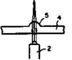
제 1 도는 본 발명의 광학식 위치 검출장치를 가진 광학식 좌표 입력장치의 검출 배치 구성을 나타낸 요부 단면도.
제 2 도는 제 1 도의 발광소자 주변의 배치를 나타낸 요부 확대도.
제 3 도는 제 1 도의 수광소자 주변의 배치를 나타낸 요부 확대도.
제 4 도는 제 1 도의 광학식 좌표 입력장치를 사용하는 상태를 나타낸 사시도이다.
* 도면의 주요부분에 대한 부호의 설명
1a,1b,1c,1d: 배열 2: LED
3: 포토트랜지스터 4: 필터
5: 집광부
본 발명은, 복수로 대향하는 발광소자와 수광소자와의 사이에 시간과 함께 순차 형성되는 복수의 광로가 차단된 위치를 검출하는 광학식 위치검출장치에 관한 것으로, 특히 검출 정밀도를 향상시킨 광학식 위치검출 장치에 관한 것이다.
광학식 위치 검출장치는 예를 들면 표시장치(예를 들어 CRT 등)의 화면을 사이에 두고, 발광소자와 수광소자를 복수조, 대향 배치하여 광성 빔(광로)의 열을 형성하고, 이 광로를 서로 교차하도록 별도 조의 발광소자와 수광소자를 복수 대향하여 배치함으로써 화면의 위치에 대응한 검출이 가능하게 된다.
이 교차하는 광로를 경시적(輕視的)으로 순차 형성하도록 구성된 광전식 터치패널(속칭; 터치 스크린)은 형성된 광로를 화면의 표시와 대응한 위치에서의 손가락이나 기타의 광차폐물로 차단하고, 차단된 시간의 정보로부터 차단된 좌표값을 얻어, 이 좌표값을 컴퓨터에 입력하도록 구성되어 있다.
이 터치스크린의 발광소자와 수광소자와의 전면은 배열된 상태를 사용자로부터 직시할 수 없도록 함과 동시에, 수광소자에 검출해야 할 광선의 파장분만큼이 도달하도록, 소정의 파장을 감쇠시키는 예를 들어 메타 크릴수지재료에 소정의 파장대역을 감쇠시키는 염료가 혼련(混練)된 성형수지로 구성되는 필터로 덮여진다. 이 필터를 배치하는 의장적인 목적을 달성하기 위해서도 발광소자와 수광소자를 적외선 영역에서 동작시키는 것을 선택하면 필터는 거의 흑색 계통으로 되기 때문에 터치 스크린 내부의 부품이 외부로부터 보이지 않게 된다.
한편, 발광소자로부터 발사되고 이에 대응하여 능동상태로 되어 수광소자에 도달하는 적외선 빔은 화면의 거리와 비례하여, 그 스폿트지름이 커진다. 그리고, 이 스폿트 지름에 의존하는 터치스크린의 검출 정밀도는 발광소자와 수광소자에 일체적으로 설치된 렌즈에 의하여 검출 가능한 거리가 제약되도록 되어 있다.
그러나, 이와 같은 광학식 위치검출 장치에 있어서는, 사용하는 용도에 따라 발광소자와 수광소자와의 간격이 제약되면 장거리가 필요한 경우에 검출할 수 없는 일이 발생한다. 이와같은 거리에 의존한 스폿트지름을 가늘게 한 적외선 빔을 얻기 위해서는 다시 발광소자와 수광소자의 광로중에서, 발광소자나 수광소자의 전면에 볼록렌즈와 같은 광학부재를 각각 배치하여, 가늘게 좁히는 방법이 고려된다.
그러나, 이 블록렌즈를 복수의 각 수광 및 발광소자의 전면에 광로의 광축에 정확하게 배치하는 일은 작업적으로 보아 극히 번잡하여 많은 시간을 필요로 하고, 또, 부품 수에서 보아도 반드시 생산효율이 양호다고는 말할 수 없다.
따라서, 본 발명은 발광소자와 수광소자의 대향간격에 따라서 필요한 검출특성이 얻어지고 생산적으로 지장이 없는 광학식 위치검출 장치를 제공하는 것을 기술적 과제로 한다.
상기 기술적 과제를 해결하기 위하여, 본 발명은 선조(線條)의 배열로 서로 대향배치된 복수의 발광소자(2)와 복수의 수광소자(3)와, 이 대향배치된 발광소자(2)와 수광소자(3)와의 소망스럽지 않는 파장성분을 감소시키기 위하여 배치된 필터(4)와, 이 필터(4)의 발광소자(2)와 수광소자(3)내의 적어도 발광소자(2)와 대향하는 위치에 일체형성된 광을 집광하는 집광부(5)를 가지는 것을 특징으로 한다.
또, 상기 선조의 배열로 서로 대향 배치된 복수의 발광소자(2)와 복수의 수광소자(3)로 구성된 1쌍의 배열(1a,1b,1c,1d)이 영상표시면을 사이에 두고 표시내용이 보이도록 배치되어 있는 것을 특징으로 한다.
또, 상기 필터(4)에 형성된 상기 집광부(5)가 소망의 광선파장을 투과하는 메타크릴 수지재료로 일체적으로 형성되어 있는 것을 특징으로 한다.
상기의 기술적 수단은, 하기와 같이 작용한다.
즉, 대향하는 발광소자와 수광소자내의 적어도 발광소자와 대향하는 필터의 위치에 집광부를 설치하여 광로의 지름을 조리도록 하였기 때문에, 거리에 따른 집광부를 일체 형성한 필터와 발광소자 배열을 대향시키는 것만으로 소망의 검출 특성을 가지는 광학식 위치검출장치가 얻어진다.
이하에, 본 발명의 일실시예를 제 1 도 내지 제 4 도에 의거하여 상세하게 설명한다. 그리고, 종래예에서 설명한 부분에 대해서는 상세한 설명을 생략한다.
제 1 도는 본 발명의 광학식 위치 검출장치를 가지는 광학식 좌표입력장치(속칭: 터치스크린)의 검출배치 구성을 나타낸 요부단면도, 제 2 도는 제 1 도의 발광소자 주변의 배치를 나타낸 요부확대도, 제 3 도는 제 1 도의 수광소자주변의 배치를 나타낸 요부확대도, 제 4 도는 제 1 도의 광학식 좌표 입력장치를 사용한 상태를 나타낸 사시도이다.
도면에 있어서, 1a,1b,1c,1d는 배열, 2는 발광소자인 LED, 3은 수광소자인 포토트랜지스터, 4는 필터, 5는 집광부를 각각 나타내고 있다.
제 1 도의 발광소자와 수광소자가 복수선조 배열로 된 배열(1a,1b,1c,1d)은 사각형의 화면을 가지는 디스플레이 장치의 4번의 화면주변에 따라 배치되어 있다. 화면의 좌측변에 따라 배치된 배열(1a)과 화면의 아래측면에 따라 배치된 배열(1b)에는 다수의 LED(2)가 배치되어 있다. 또, 화면의 우측변에 따라 배치된 배열(1c)과 화면의 위측변에 따라 배치된 배열(1d)에는 다수의 포토트랜지스터(3)의 배열이 LED(2)와 각각 대향하여 배치되어 있다. 그리고, LED(2)와 포토트랜지스터(3)의 사이에 순차 발생하는 적외선 빔은 메트릭스형상으로 형성되도록 구성된다.
한편, LED(2) 및 포토트랜지스터(3)와 화면과의 사이에는 제1도 및 제4도에 나타낸 바와 같이 4변을 가지는 틀형상의 필터(4)가 배치되어 있다. 이 필터(4)의 화면에 인접하는 면측에 설치된 복수의 집광부(5)는 LED(2)와 트랜지스터(3)와의 배열피치에 대응하여 각각 형성된다. 이 복수의 집광부(5)는 구면(球面)형상으로 돌출하여 필터(4)와 일체적으로 형성되어 볼록렌즈가 구성된다. 이 볼록렌즈인 집광부(5)가 대향배치된 LED(2)로부터 투광된 적외선광은 제 2 도에 나타낸 바와 같이 수광소자측을 향해 퍼지는 빔을 소정의 특성으로 조리므로써 소망의 빔스폿지롬이 수광소자 측에서 얻어지게 된다. 또, 포토트랜지스터(3)와 대향하는 볼록렌즈인 집광부(5)는 제3도에 나타낸 바와 같이 발광소자측으로부터의 광을 집광하여 대부분의 적외선 광을 포토트랜지스터(3)에 공급하도록 되어 있다.
이상, 설명한 바와 같이, 본 발명에 의하면, 용도별로 설정된 형상의 필터의 적어도 발광소자측에 집광부를 일체적으로 형성하였기 때문에, 소정의 적외선 빔의 스폿지름을 얻는데 부품수를 증가시킴없이 조립작업도 극히 간략화된 상태에서 행할 수가 있고, 부품의 고정에 관한 품질도 안정하게 유지될 수 있는 효과를 가진다.
Claims (3)
- 선조의 배열로 서로대향 배치된 복수의 발광 소자(2)와 복수의 수광소자(3)와, 상기 대향 배치된 발광소자(2)와 수광소자(3)와의 사이에 소망스럽지 않는 파장성분을 감쇠시키기 위하여 배치된 필터(4)와, 이 필터(4)의 발광소자(2)와 수광소자(3)내에 적어도 발광소자(2)와 대향하는 위치에 일체형성된 광을 집광하는 집광부(5)를 가진 것을 특징으로 하는 광학식 위치 검출장치.
- 제1항에 있어서, 상기 선조의 배열이 서로 대향 배치된 복수의 발광소자(2)와 복수의 수광소자(3)로 구성된 1쌍의 배열(1a,1b,1c,1d)이 화상표시면을 사이에 두고 표시내용이 보이도록 배치되어 있는 것을 특징으로 하는 광학식 위치검출장치.
- 제1항에 있어서, 상기 필터(4)에 형성된 집광부(5)가 소망의 광선 파장을 투과하는 메타크릴수지 재료에 의해 일체적으로 형성되는 것을 특징으로 하는 광학식 위치 검출장치.
Applications Claiming Priority (2)
| Application Number | Priority Date | Filing Date | Title |
|---|---|---|---|
| JP60105326A JPS61262917A (ja) | 1985-05-17 | 1985-05-17 | 光電式タツチパネルのフイルタ− |
| JP85-105326 | 1985-05-17 |
Publications (2)
| Publication Number | Publication Date |
|---|---|
| KR860009333A KR860009333A (ko) | 1986-12-22 |
| KR900003229B1 true KR900003229B1 (ko) | 1990-05-11 |
Family
ID=14404591
Family Applications (1)
| Application Number | Title | Priority Date | Filing Date |
|---|---|---|---|
| KR1019860000776A KR900003229B1 (ko) | 1985-05-17 | 1986-02-05 | 광학실 위치 검출장치 |
Country Status (5)
| Country | Link |
|---|---|
| US (1) | US4737631A (ko) |
| JP (1) | JPS61262917A (ko) |
| KR (1) | KR900003229B1 (ko) |
| DE (1) | DE3616601A1 (ko) |
| GB (1) | GB2175393B (ko) |
Families Citing this family (49)
| Publication number | Priority date | Publication date | Assignee | Title |
|---|---|---|---|---|
| US4812830A (en) * | 1986-12-08 | 1989-03-14 | Digital Electronics Corporation | Touch panel display assembly |
| US4891508A (en) * | 1988-06-30 | 1990-01-02 | Hewlett-Packard Company | Precision infrared position detector apparatus for touch screen system |
| US5162783A (en) * | 1990-07-23 | 1992-11-10 | Akzo N.V. | Infrared touch screen device for a video monitor |
| US6972753B1 (en) * | 1998-10-02 | 2005-12-06 | Semiconductor Energy Laboratory Co., Ltd. | Touch panel, display device provided with touch panel and electronic equipment provided with display device |
| JP3481498B2 (ja) * | 1999-04-28 | 2003-12-22 | 日本航空電子工業株式会社 | 光学式タッチパネル |
| JP4052498B2 (ja) | 1999-10-29 | 2008-02-27 | 株式会社リコー | 座標入力装置および方法 |
| JP2001184161A (ja) | 1999-12-27 | 2001-07-06 | Ricoh Co Ltd | 情報入力方法、情報入力装置、筆記入力装置、筆記データ管理方法、表示制御方法、携帯型電子筆記装置および記録媒体 |
| US6864882B2 (en) | 2000-05-24 | 2005-03-08 | Next Holdings Limited | Protected touch panel display system |
| US6690363B2 (en) | 2000-06-19 | 2004-02-10 | Next Holdings Limited | Touch panel display system |
| US6803906B1 (en) * | 2000-07-05 | 2004-10-12 | Smart Technologies, Inc. | Passive touch system and method of detecting user input |
| EP1739528B1 (en) * | 2000-07-05 | 2009-12-23 | Smart Technologies ULC | Method for a camera-based touch system |
| US8156525B2 (en) * | 2002-05-20 | 2012-04-10 | Sony Corporation | Information-processing system, information-processing device, and information-processing method |
| KR100487483B1 (ko) * | 2002-06-29 | 2005-05-06 | (주) 인펙 | 광학식 터치패널과 광학식 터치패널용 발광소자 |
| US6954197B2 (en) * | 2002-11-15 | 2005-10-11 | Smart Technologies Inc. | Size/scale and orientation determination of a pointer in a camera-based touch system |
| US6972401B2 (en) * | 2003-01-30 | 2005-12-06 | Smart Technologies Inc. | Illuminated bezel and touch system incorporating the same |
| US7629967B2 (en) | 2003-02-14 | 2009-12-08 | Next Holdings Limited | Touch screen signal processing |
| US8456447B2 (en) | 2003-02-14 | 2013-06-04 | Next Holdings Limited | Touch screen signal processing |
| US8508508B2 (en) * | 2003-02-14 | 2013-08-13 | Next Holdings Limited | Touch screen signal processing with single-point calibration |
| US7532206B2 (en) | 2003-03-11 | 2009-05-12 | Smart Technologies Ulc | System and method for differentiating between pointers used to contact touch surface |
| US7411575B2 (en) * | 2003-09-16 | 2008-08-12 | Smart Technologies Ulc | Gesture recognition method and touch system incorporating the same |
| US7274356B2 (en) | 2003-10-09 | 2007-09-25 | Smart Technologies Inc. | Apparatus for determining the location of a pointer within a region of interest |
| US7355593B2 (en) | 2004-01-02 | 2008-04-08 | Smart Technologies, Inc. | Pointer tracking across multiple overlapping coordinate input sub-regions defining a generally contiguous input region |
| US7232986B2 (en) * | 2004-02-17 | 2007-06-19 | Smart Technologies Inc. | Apparatus for detecting a pointer within a region of interest |
| US7460110B2 (en) | 2004-04-29 | 2008-12-02 | Smart Technologies Ulc | Dual mode touch system |
| US7492357B2 (en) | 2004-05-05 | 2009-02-17 | Smart Technologies Ulc | Apparatus and method for detecting a pointer relative to a touch surface |
| US7538759B2 (en) | 2004-05-07 | 2009-05-26 | Next Holdings Limited | Touch panel display system with illumination and detection provided from a single edge |
| US8120596B2 (en) | 2004-05-21 | 2012-02-21 | Smart Technologies Ulc | Tiled touch system |
| CA2588806A1 (en) * | 2004-12-09 | 2006-06-15 | Rpo Pty Limited | Optical power distribution devices |
| US20070165007A1 (en) * | 2006-01-13 | 2007-07-19 | Gerald Morrison | Interactive input system |
| US20070165008A1 (en) * | 2006-01-17 | 2007-07-19 | International Business Machines Corporation | Compact infrared touch screen apparatus |
| US20070205994A1 (en) * | 2006-03-02 | 2007-09-06 | Taco Van Ieperen | Touch system and method for interacting with the same |
| US9442607B2 (en) | 2006-12-04 | 2016-09-13 | Smart Technologies Inc. | Interactive input system and method |
| EP2135155B1 (en) | 2007-04-11 | 2013-09-18 | Next Holdings, Inc. | Touch screen system with hover and click input methods |
| US8094137B2 (en) | 2007-07-23 | 2012-01-10 | Smart Technologies Ulc | System and method of detecting contact on a display |
| US8432377B2 (en) | 2007-08-30 | 2013-04-30 | Next Holdings Limited | Optical touchscreen with improved illumination |
| AU2008280952A1 (en) * | 2007-08-30 | 2009-03-19 | Next Holdings Ltd | Low profile touch panel systems |
| US8405636B2 (en) | 2008-01-07 | 2013-03-26 | Next Holdings Limited | Optical position sensing system and optical position sensor assembly |
| WO2009137355A2 (en) * | 2008-05-06 | 2009-11-12 | Next Holdings, Inc. | Systems and methods for resolving multitouch scenarios using software filters |
| US8902193B2 (en) | 2008-05-09 | 2014-12-02 | Smart Technologies Ulc | Interactive input system and bezel therefor |
| US8676007B2 (en) | 2008-06-19 | 2014-03-18 | Neonode Inc. | Light-based touch surface with curved borders and sloping bezel |
| TWI406045B (zh) * | 2008-06-30 | 2013-08-21 | Ibm | 具有smt元件作為光閘之光學接觸面板及在該面板上之形成光閘的方法 |
| US20100079385A1 (en) * | 2008-09-29 | 2010-04-01 | Smart Technologies Ulc | Method for calibrating an interactive input system and interactive input system executing the calibration method |
| US8339378B2 (en) * | 2008-11-05 | 2012-12-25 | Smart Technologies Ulc | Interactive input system with multi-angle reflector |
| US20100229090A1 (en) * | 2009-03-05 | 2010-09-09 | Next Holdings Limited | Systems and Methods for Interacting With Touch Displays Using Single-Touch and Multi-Touch Gestures |
| US8692768B2 (en) | 2009-07-10 | 2014-04-08 | Smart Technologies Ulc | Interactive input system |
| US20110095977A1 (en) * | 2009-10-23 | 2011-04-28 | Smart Technologies Ulc | Interactive input system incorporating multi-angle reflecting structure |
| JP5525798B2 (ja) * | 2009-11-20 | 2014-06-18 | 株式会社ニューフレアテクノロジー | 荷電粒子ビーム描画装置およびその帯電効果補正方法 |
| US20110193969A1 (en) * | 2010-02-09 | 2011-08-11 | Qisda Corporation | Object-detecting system and method by use of non-coincident fields of light |
| CN116420125A (zh) | 2020-09-30 | 2023-07-11 | 内奥诺德公司 | 光学触摸传感器 |
Family Cites Families (7)
| Publication number | Priority date | Publication date | Assignee | Title |
|---|---|---|---|---|
| US4015122A (en) * | 1974-07-12 | 1977-03-29 | Rubinstein Walter M | Photo-electric object detection system |
| US4384201A (en) * | 1978-04-24 | 1983-05-17 | Carroll Manufacturing Corporation | Three-dimensional protective interlock apparatus |
| US4267443A (en) * | 1978-04-24 | 1981-05-12 | Carroll Manufacturing Corporation | Photoelectric input apparatus |
| DE3025318C2 (de) * | 1980-07-04 | 1982-05-19 | Hewlett-Packard France S.A., Eybens | Sensor-Matrix für Bildschirme |
| US4467193A (en) * | 1981-09-14 | 1984-08-21 | Carroll Manufacturing Corporation | Parabolic light emitter and detector unit |
| DE3147185A1 (de) * | 1981-11-27 | 1983-06-01 | Sony Corp., Tokyo | Verfahren zum steuern einer elektronischen einrichtung und vorrichtung zur durchfuehrung des verfahrens |
| GB2159269A (en) * | 1984-05-21 | 1985-11-27 | Fuscone Roy | Optical score identifier for target games |
-
1985
- 1985-05-17 JP JP60105326A patent/JPS61262917A/ja active Pending
-
1986
- 1986-02-05 KR KR1019860000776A patent/KR900003229B1/ko not_active IP Right Cessation
- 1986-05-16 DE DE19863616601 patent/DE3616601A1/de active Granted
- 1986-05-19 US US06/864,709 patent/US4737631A/en not_active Expired - Lifetime
- 1986-05-19 GB GB8612106A patent/GB2175393B/en not_active Expired
Also Published As
| Publication number | Publication date |
|---|---|
| KR860009333A (ko) | 1986-12-22 |
| GB8612106D0 (en) | 1986-06-25 |
| GB2175393A (en) | 1986-11-26 |
| DE3616601A1 (de) | 1986-11-20 |
| US4737631A (en) | 1988-04-12 |
| DE3616601C2 (ko) | 1989-12-21 |
| GB2175393B (en) | 1989-07-19 |
| JPS61262917A (ja) | 1986-11-20 |
Similar Documents
| Publication | Publication Date | Title |
|---|---|---|
| KR900003229B1 (ko) | 광학실 위치 검출장치 | |
| JP4122065B2 (ja) | コンピュータシステム用ユーザー入力装置 | |
| US4737626A (en) | Photoelectric touch panel having reflector and transparent photoconductive plate | |
| US4933544A (en) | Touch entry apparatus for cathode ray tube with non-perpendicular detection beams | |
| US5572251A (en) | Optical position detecting unit and optical coordinate input unit | |
| US5196836A (en) | Touch panel display | |
| US4837430A (en) | Photoelectric touch panel having parallel light emitting and detecting arrays separated by a light shield | |
| US4742221A (en) | Optical coordinate position input device | |
| US4751379A (en) | Touch panel coordinate input device having light filter | |
| US7705835B2 (en) | Photonic touch screen apparatus and method of use | |
| KR100804815B1 (ko) | 외란광에 강한 적외선 카메라를 이용한 터치스크린 | |
| JPH053012B2 (ko) | ||
| US4818859A (en) | Low profile opto-device assembly with specific optoelectronic lead mount | |
| JPH0357563B2 (ko) | ||
| GB2082427A (en) | A sensor matrix for display screens | |
| US4739160A (en) | Optical coordinate data entry device with integral lens and spacer | |
| KR900004015B1 (ko) | 좌표 입력 장치 | |
| JPH0326848B2 (ko) | ||
| EP0520669B1 (en) | Touch input device | |
| JPS6174024A (ja) | 位置検出装置 | |
| JPS63187726A (ja) | 光学式タツチ・スイツチ装置におけるキ−画像表示方法 | |
| RU2278423C1 (ru) | Устройство для интерактивной локализации объектов | |
| JPH05189123A (ja) | タッチスイッチ装置 | |
| JP3218575B2 (ja) | 液晶タッチパネル | |
| WO2008034191A1 (en) | Signal detection for optical touch input devices |
Legal Events
| Date | Code | Title | Description |
|---|---|---|---|
| A201 | Request for examination | ||
| E902 | Notification of reason for refusal | ||
| G160 | Decision to publish patent application | ||
| E701 | Decision to grant or registration of patent right | ||
| GRNT | Written decision to grant | ||
| LAPS | Lapse due to unpaid annual fee |