KR860001344B1 - Digital data code conversion circuit for variable word-length data code - Google Patents
Digital data code conversion circuit for variable word-length data code Download PDFInfo
- Publication number
- KR860001344B1 KR860001344B1 KR1019830002965A KR830002965A KR860001344B1 KR 860001344 B1 KR860001344 B1 KR 860001344B1 KR 1019830002965 A KR1019830002965 A KR 1019830002965A KR 830002965 A KR830002965 A KR 830002965A KR 860001344 B1 KR860001344 B1 KR 860001344B1
- Authority
- KR
- South Korea
- Prior art keywords
- data
- circuit
- data code
- variable
- output
- Prior art date
Links
Images


Classifications
-
- H—ELECTRICITY
- H03—ELECTRONIC CIRCUITRY
- H03M—CODING; DECODING; CODE CONVERSION IN GENERAL
- H03M7/00—Conversion of a code where information is represented by a given sequence or number of digits to a code where the same, similar or subset of information is represented by a different sequence or number of digits
- H03M7/30—Compression; Expansion; Suppression of unnecessary data, e.g. redundancy reduction
- H03M7/40—Conversion to or from variable length codes, e.g. Shannon-Fano code, Huffman code, Morse code
Abstract
Description
제1a도는 가변어장 데이타 코우드를 부호화하고 전송하는 시스템의 블록도.1A is a block diagram of a system for encoding and transmitting a variable length data code.
제1b도는 가변어장 데이타 코우드를 수신하여 해독하는 시스템의 블록도.1B is a block diagram of a system for receiving and decoding a variable fish field data code.
제2도는 고정어장(fixed-word-length) 데이타 코우드를 가변어장 데이타 코우드로 변환하는 변경표의 일예.2 is an example of a change table for converting a fixed-word-length data code to a variable-length data code.
제3도는 종래의 가변어장 데이타 코우드용 디지탈 데이타 코우드 변환회로의 블록도.3 is a block diagram of a conventional digital data code conversion circuit for a variable fish field data code.
제4도는 제3도의 변환회로 입력 데이타열 및 대응하는 출력 데이타열의 일예.4 is an example of the conversion circuit input data string and corresponding output data string of FIG.
제5도는 본 발명에 따른 가변어장 데이타 코우드용 디지탈 데이타 코우드 변환회로의 블록도.5 is a block diagram of a digital data code conversion circuit for a variable-length data code according to the present invention.
제6도는 제5도 변환회로에서 준비회로의 일실시예의 회로도.6 is a circuit diagram of one embodiment of a preparation circuit in the FIG. 5 conversion circuit;
제7도는 제6도 준비회로에서 변환된 어장정보용 변환표.7 is a conversion table for fishery information converted in the FIG. 6 preparation circuit.
제8도는 제6도 준비회로의 주부분의 상세회로도.8 is a detailed circuit diagram of the main part of the FIG.
제9도는 제5도 변환회로에서 데이타 코우드 변환부의 일실시예의 회로도.9 is a circuit diagram of an embodiment of a data code conversion unit in the FIG. 5 conversion circuit.
제10도는 제9도 데이타 코우드 변환부의 변환동작을 보여주는 설명도.FIG. 10 is an explanatory diagram showing a conversion operation of a data code conversion unit of FIG.
제11도는 제9도에서 회전회로의 상세회로도.11 is a detailed circuit diagram of a rotating circuit in FIG.
제12도는 제9도에서 제1선택기 회로의 상세회로도.12 is a detailed circuit diagram of the first selector circuit in FIG.
제13도는 제9도에서 제2선택기회로의 상세회로도.FIG. 13 is a detailed circuit diagram of the second selector circuit in FIG.
제14도는 제13도 제2선택기회로의 제어신호용변환표.14 is a conversion table for control signals of the 13th selector circuit.
* 도면의 주요부분에 대한 부호의 설명* Explanation of symbols for main parts of the drawings
1 : 디지탈데이타코우드변환회로 3 : 준비회로1: digital data conversion circuit 3: preparation circuit
4 : 데이타코우드변환부 11 : 펄스코오드변조기4: data code converter 11: pulse code modulator
12 : 감산기 13 : 양자화회로12
14, 24 : 가산기 15 : 예측회로14, 24: adder 15: prediction circuit
16, 23 : D/D변환기16, 23: D / D converter
17, 22 : 디지탈데이타코우드변환회로17, 22: digital data conversion circuit
18, 21 : 버퍼메모리 22 : 적분회로18, 21: buffer memory 22: integrating circuit
본 발명은 가변어장(Variable-word-length) 데이타 코우드용 디지탈 데이타 코우드 변환회로에 관한 것이다. 좀더 상세하게는 본 발명은 병렬로 공급된 입력가변어장 데이타 코우드를 소정 길이보다 작거나 동일한 워어드 길이를 가진 데이타 코우드로 분할하는 준비회로가 갖추어진 가변어장 데이타 코우드용 디지탈 데이타 코우드용 디지탈 데이타 코우드 변환회로에 관한 것이다.The present invention relates to a digital data code conversion circuit for a variable-word-length data code. More specifically, the present invention relates to a digital data code for a variable data data code having a preparatory circuit for dividing the input variable length data code supplied in parallel into a data code having a word length less than or equal to a predetermined length. It relates to a digital data code conversion circuit.
일반적으로 정보데이타 전송에 있어서, 두 형태의 데이타 코우딩 시스템이 이용된다.In general, in the transmission of information data, two types of data coding systems are used.
① 한 형태는 일 워어드(word)에 포함된 비트수가 정보의 내용에 따라서 변환되는 가변어장 데이타 코우딩 시스템이고, ② 다른 한 형태는 일 워어드내에 포함된 비트수가 항상 일정한 고정어장 데이타 코우딩시스템이다. 가변어장 데이타 코우딩 시스템은 동일한 정보에 필요로 되는 총비트수가 고정어장 데이타 코우딩시스템과 비교할 때 매우 적게된다는 이점이 있다.① One type is a variable length data coding system in which the number of bits contained in a word is converted according to the content of information. ② The other type is a fixed length data coding in which the number of bits contained in a word is always constant. System. The variable length data coding system has the advantage that the total number of bits required for the same information is very small compared to the fixed length data coding system.
따라서 가변어장 데이타 코우딩 시스템은 영상신호, 음성신호 등의 전송에 넓게 이용된다. 그러나 가변어장 데이타 코우딩 시스템에서 일 워어드에 포함된 비트수는 각 워어드마다 다르다.Therefore, the variable fish field data coding system is widely used for transmission of video signals, audio signals and the like. However, in variable length data coding systems, the number of bits included in a word is different for each word.
따라서 어떠한 변환없이 다른 어장(word-lenfth)을 가진 데이타 워어드를 처리하는데 불편하며 데이타워어드를 처리하는 회로구성이 복잡하게 된다.Therefore, it is inconvenient to process datawords with different word-lenfth without any conversion, and the circuit configuration for processing datawords is complicated.
이러한 가변어장 데이타 코우딩 시스템의 단점은 다른 길이를 가진 데이타 코우드열을 분할하고 조합하여 일정한 길이를 가진 병렬데이타 코우드 열로 변환함에 의해서 제거될 수 있다. 이것을 수행하기 위하여 가변어장 데이타 코우드를 고정어장 데이타 코우드로 변환하는 변환회로가 요구된다.The disadvantage of this variable length data coding system can be eliminated by dividing and combining data code sequences having different lengths into parallel data code sequences having a constant length. To accomplish this, a conversion circuit for converting the variable length data code to the fixed length data code is required.
가변어장 데이타 코우드용 종래의 디지탈 데이타 코우드 변환회로는 일본특허출원 번호55-017,259에 밝혀져 있다. 이 디지탈 데이타 코우드 변환회로에 있어서, n비트까지의 어장을 가진 가변어장 데이타 코우드에 대한 코우드 패턴정보는 데이타 입력단자를 통하여 병렬로 입력되며 입력 가변어장 데이타 코우드의 비트수를 나타내는 워어드 길이 정보가 워어드 길이 입력단자를 통하여 입력된다. 입력 가변어장 데이타 코우드는 변환회로에서 변환되어 n비트를 가진 고정어장 데이타 코우드가 출력된다.A conventional digital data code conversion circuit for a variable fish field data code is disclosed in Japanese Patent Application No. 55-017,259. In this digital data code conversion circuit, code pattern information for a variable-length data code having a length of up to n bits is input in parallel through a data input terminal and represents a number of bits of an input variable-length data code. Adword length information is input via a word length input terminal. The input variable length data code is converted by the conversion circuit to output a fixed length data code having n bits.
상기한 디지탈 데이타 코우드 변환회로에 있어서 변환회로에 의해 처리된 데이타 코우드의 어장은 n비트 보다 작거나 동일한 것이 요구되기 때문에 입력 가변어장 데이타 코우드의 최대 비트수가 더 클 경우에는 병렬로 처리된 비트수(n)를 더 크게하는 것이 필요하다. 이것은 회로구조가 복잡하게 되고 장치의 크기가 더 크게되는 것을 의미한다.In the above digital data code conversion circuit, since the data coded by the conversion circuit is required to be smaller than or equal to n bits, when the maximum number of bits of the input variable length data code is larger, the parallel processing is performed in parallel. It is necessary to make the bit number n larger. This means that the circuit structure becomes complicated and the device size becomes larger.
본 발명의 주목적은 입력 가변어장 데이타 코우드를 소정값보다 작거나 동일한 어장을 가진 데이타 코우드로 분할하는 준비회로가 갖추어져서 출력 고정어장 데이타의 길이보다 더 큰 어장을 가진 데이타 코우드가 처리 가능하게 되어 매우 큰 어장을 가진 입력 데이타 코우드가 비교적 작은 회로크기를 가진 장치에 의해서 처리될 수 있는 가변어장 코우드용 디지탈 데이타 코우드 변환회로를 제공하는 것이다.The main object of the present invention is to provide a preparation circuit for dividing the input variable-length data code into data codes having a fishing field smaller than or equal to a predetermined value so that the data code having a fishing field larger than the length of the output fixed-length data can be processed. In order to provide a digital data code conversion circuit for a variable fish field code, an input data code having a very large fishing field can be processed by a device having a relatively small circuit size.
본 발명의 다른 목적은 제어회로 및 제어동작의 구성이 단순화 될 수 있는 가변어장 데이타 코우드용 디지탈 데이타 코우드 변환회로를 제공하는 것이다.Another object of the present invention is to provide a digital data code conversion circuit for a variable fish field data code, in which the configuration of the control circuit and the control operation can be simplified.
본 발명에 따르면 어장정보에 따라서 입력 가변어장 데이타 코우드를 분할하고 조합함에 의해서 소정수(n)보다 더 적거나 동일한 어장을 가진 가변어장 데이타 코우드를 소정수(n)와 동일한 어장을 가진 고정 데이타 코우드로 변환하는 데이타 코우드 변환부 및 데이타 코우드 변환부의 앞단에 배치되어 소정수(n)보다 작거나 동일한 어장을 가진 상이한 가변어장 데이타 코우드로 분할하고 분할된 가변어장 데이타 코우드에 대하여 어장정보를 발생하는 준비회로로 구성되어 상기 데이타 코우드 변환부는 가변어장 데이타 코우드 분할수에 따라 곱해진 데이타 입력율에 비례하는 동작속도로 동작되는 가변어장 데이타 코우드용 디지탈 데이타 코우드 변환회로가 제공된다.According to the present invention, by dividing and combining the input variable fishery data code according to the fishery information, the variable fishery data code having less or equal to the predetermined number (n) is fixed to have the same fishery as the predetermined number (n). A data code converter converting the data code and the data code converter are arranged in front of each other and divided into different variable-length data codes having a fishing field smaller than or equal to a predetermined number (n). The data code conversion unit, which is configured as a preparation circuit for generating information, operates at an operation speed that is proportional to the data input rate multiplied by the variable number of data field divisions. Is provided.
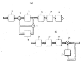
본 발명의 바람직한 실시예를 설명하기전에 가변어장 데이타 코우드를 부호화하고 해독하는 시스템이 본 발병에 따른 데이타 코우드 변환회로가 적용된 시스템에 설명된다. 가변어장 데이타 코우드를 부호화하는 시스템이 제1a도에 나타나 있으며, 가변어장 데이타 코우드를 해독하는 시스템이 제1a도에 나타나 있다.Prior to describing the preferred embodiment of the present invention, a system for encoding and decoding variable-length data code is described in a system to which a data code conversion circuit according to the present invention is applied. A system for encoding a variable length data code is shown in FIG. 1a, and a system for decoding a variable length data code is shown in FIG.
제1a도의 시스템은 펄스코우드변조기(11), 감산기(12), 양자화회로(13), 가산기(14), 예측회로(15), 디지탈/디지탈 변환기(16), 디지탈 데이타 코우드 변환회로(17) 및 버퍼메모리(18)로 이루어져 있다.The system of FIG. 1A includes a
제1a도의 시스템에서 영상신호 또는 음성신호와 같은 입력데이타 신호는 펄스코우드 변조기(11)에 공급되어 병렬 8비트 펄스코우드변조(PCM) 데이타 코우드가 펄스코우드 변조기(11)부터 출력된다. PCM데이타 코우드는 감산기(12)에 공급되어 예측회로 (15)로부터 예측값에 의해서 감산되며 그다음 양자화회로(13)에 공급된다.In the system of FIG. 1A, an input data signal such as a video signal or an audio signal is supplied to a
양자화회로(13)에서 공급된 데이타 코우드는 몇개의 양자레벨, 예를 들면 8레벨 혹은 16레벨로 양자화되어 1양자레벨 신호가 양자화회로(13)로부터 출력된다.The data code supplied from the
양자레벨신호는 가산기(14)와 디지탈/디지탈 변환기(16)에 공급된다. 가산기 (14)에서 양자레벨신호는 전의 예측값에 가산되어 다음의 예측값으로서 예측회로에 공급된다. 디지탈/디지탈 변환기(16)에서 양자레벨신호는 가변어장 데이타 코우드로 변환된다.The quantum level signal is supplied to the
가변어장 데이타 코우드의 일예가 제2도에 나타나 있다. 제2도에서 입력 데이타는 16양자레벨로 양자화되며 이들 각 양자레벨은 제2도에 표시된 바와 같이 4비트의 일데이타패턴에 대응한다. 이 양자레벨들(즉 데이타패턴)은 1비트로부터 16비트까지 서로 다른 어장을 가진 가변어장 데이타 코우드로 변환된다.An example of a variable fish field data code is shown in FIG. In FIG. 2, input data is quantized to 16 quantum levels, and each of these quantum levels corresponds to a 4-bit one data pattern as shown in FIG. These quantum levels (i.e. data patterns) are converted into variable length data code with different lengths from 1 bit to 16 bits.
각 가변어장 데이타 코우드의 어장은 작은 절대값을 갖는 양자레벨에 대응하는 데이타 코우드가 짧은 어장을 갖도록 설정된다. 양자회로(13)로부터 출력된 양지레벨 신호는 실제신호 데이타와 그것은 예측값 사이의 차를 나타내므로 출력양자 레벨신호 예의 대부분은 작은 절대값을 갖는다.The fishing field of each variable-field data code is set such that the data code corresponding to the quantum level having a small absolute value has a short fishing field. Since the positive level signal output from the
따라서 디지탈/디지탈 변환기(16)로부터 출력되는 가변어장 데이타 코우드의 평균어장은 매우 작아 예를라면 2 또는 3비트로 된다. 따라서 전송될 정보의 전체데이타 길이는 PCM데이타 코우드에서 보다 가변어장 데이타 코우드에서 더 짧게 된다.Therefore, the average length of the variable length data code output from the digital-to-
디지탈/디지탈 변환기(16)로부터 출력된 가변어장 데이타 코우드는 디지탈 데이타 코우드 변환회로(17)에 공급되어 고정어장 데이타 코우드로 변환된다. 디지탈 데이타 코우드 변환회로(17)의 동작은 뒤에 상세히 기술된다. 변환회로(17)로부터의 고정어장 데이타 고우드는 버퍼메모리(18)에 공급되어 기억된다. 기억된 데이타 코우드는 전송회로(표시 않됨)에 의해 전송된다.The variable length data code output from the digital /
제1b도의 가변어장 데이타 코우드를 해독하는 시스템은 버퍼메모리(21), 디지탈 데이타 코우드 변환회로(22), 디지탈/디지탈 변환기(33), 가산기(24) 및 직분회로(25)로 구성되어 있다. 제1b도 시스템에서 제1a도 시스템으로부터 전송된 수신데이타 코우드는 버퍼메모리(21)에 기억된다. 기억된 데이타 코우드는 디지탈 데이타 코우드 변환회로(22)에 공급되어 제2도에 표시된 바와 같이 가변어장 데이타 코우드로 역으로 변환된다. 변환회로(22)로부터의 가변어장 데이타 코우드는 디지탈 디지탈, 변환기(23)에 공급되어 역으로 양자레벨 신호로 변환된다.The system for decoding the variable fish field data code of FIG. 1B is composed of a
변환기(23)의 양자레벨 신호는 가산기(24)에 공급되어 적분회로(25)로부터의 출력 데이타 코우드에 가산된다. 따라서 가산기(24)로부터의 출력 데이타 코우드는 재생산된 PCM데이타 코우드로서 출력된다.The quantum level signal of the
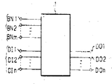
제1도 시스템에 이용될 수 있는 가변어장 데이타 코우드용의 종래의 디지탈 데이타 코우드 변환회로가 제3도에 표시되어 있다.A conventional digital data code conversion circuit for a variable fish field data code that can be used in the FIG. 1 system is shown in FIG.
제3도의 디지탈 데이타 코우드 변환회로(1)는 n비트 코우드패턴 정보입력단자(DI1, DI2, …, DIn), m비트어장 정보 입력단자(BN1, BN2, …, BNm) 및 n비트 출력단자(DO1, DO2, …, DOn)를 갖는다. 제3도의 디지탈 데이타 코우드 변환회로(1)에서, 코우드 패턴 정보 입력단자(DI1, DI2, …, DIn)로부터 입력되는 가변어장 데이타 코우드는 고정어장 데이타 코우드로 변환되어 변환된 n비트 고정어장 데이타 코우드는 출력단자(DO1, DO2, …, DOn)로부터 출력된다.The digital data
제3도의 디지탈 데이타 코우드 변환회로(1)의 동작은 제4도의 입력 및 출력 데이타예를 참고로 기술된다.The operation of the digital data
제4도의 예에서 8비트보다 더 적거나 동일한 어장을 가진 가변어장 데이타코우드로서 입력데이타열(A), (B), …, (F)은 순차적으로 디지탈 데이타 코우드 변환회로(1)로 입력된다. 제1입력 데이타(A)가 6비트 데이타이므로 다음 입력데이타(B)의 앞의 2비트는 입력데이타(A)의 끝에 부착되어 8비트 출력데이타(A')가 출력된다.In the example of FIG. 4, as a variable-length data code having a length less than or equal to 8 bits, input data strings (A), (B),. , (F) are sequentially input to the digital data
그다음, 입력 데이타(B)의 최후의 1비트는 남으므로 다음 입력 데이타( C)의 앞의 7비트가 남은 1비트에 부착되어 8비트 출력 데이타(B')가 출력된다. 입력 데이타(C)의 최후의 1비트가 남으므로 다음 입력 데이타(D)의 전 4비트는 남은 1비트에 부착된다.Then, since the last 1 bit of the input data B is left, the first 7 bits of the next input data C are appended to the remaining 1 bit and 8-bit output data B 'is output. Since the last one bit of the input data C remains, all four bits of the next input data D are appended to the remaining one bit.
더우기 다음 입력 데이타(E)의 앞의 3비트는 입력 데이타(D)의 4비트에 부착되여 8비트 출력 데이타(C')가 출력된다. 다음에, 입력 데이타(E)의 최후의 2비트는 남게 되므로 다음 입력 데이타(F)의 6비트가 남은 2개 비트에 부착되어 8비트 출력 데이타(D')가 출력된다.Furthermore, the first 3 bits of the next input data E are attached to 4 bits of the input data D, and 8-bit output data C 'is output. Next, since the last two bits of the input data E remain, 6 bits of the next input data F are attached to the remaining two bits, and 8-bit output data D 'is output.
상기한 바와 같이 입력 가변어장 데이타 코우드는 설명한 바와 같은 입력 데이타 코우드를 분할하고 조합함에 의해서 출력 고정어장 데이타 코우드로 변환된다. 상기한 변환동작은 앞의 일본특허출원 번호 55-017,259에 밝혀진 회로에 의해서 수행될 수 있다.As described above, the input variable-length data code is converted into an output fixed-length data code by dividing and combining the input data code as described above. The above converting operation can be performed by the circuit disclosed in Japanese Patent Application No. 55-017,259.
그러나 상기한 디지탈 데이타 코우드 변환회로 입력 가변어장 데이타 코우드의 어장은 소정수(n)보다 적거나 동일함이 틀림없다. 따라서 n보다 더 큰 워어드 길이를 가진 입력 데이타 코우드는 데이타 코우드 변환회로에 의해서 처리될 수 없다. 예를 들면 제2도에 나타난 최고 16비트를 가질 수 있는 가변어장 데이타 코우드는 상기한 8비트 데이타 코우드 변환회로에 의해서 처리될 수 없다.However, the field of the digital data code conversion circuit input variable-field data code described above must be less than or equal to the predetermined number n. Therefore, input data code with a word length greater than n cannot be processed by the data code conversion circuit. For example, the variable length data code, which may have up to 16 bits shown in FIG. 2, cannot be processed by the 8-bit data code conversion circuit described above.
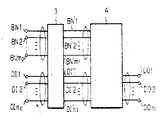
본 발명에 따른 가변어장 데이타 코우드용의 디지탈 데이타 코우드 변환회로가 제5도에 나타나 있다. 제5도의 디지탈 데이타 코우드 변환회로는 준비회로(3) 및 데이타 코우드 변환부(4)로 구성되어 있다. 제5도의 데이타 코우드 변환회로에 있어서, 준비회로(3)는 가변어장 데이타 패턴 입력단자(DI1, DI2, …, DIn0), 어장 입력단자(BN1, BN2, …, BNm0), 가변어장 데이타 패턴 출력단자(DI'1, BN'2, …, BN'm1) 및 어장 출력단자를 갖는다.A digital data code conversion circuit for a variable fish field data code according to the present invention is shown in FIG. The digital data code conversion circuit of FIG. 5 is composed of a
준비회로(3)에서 n0보다 적거나 동일한 워어드 길이를 가진 입력 가변어장 데이타 코우드는 n1(n1<n0)보다 적거나 동일한 워어드 길이를 가진 가변어장 데이타 코우드로 분할된다. 예를 들면, 만약 n0=16, n1=8이고 15비트 데이타 코우드가 준비회로(3)로 입력될 때 15비트 데이타 코우드는 각각 8비트 및 7비트를 가진 두개의 데이타 코우드로 분할된다. 15비트를 나타내는 한개의 어장정보는 15비트 데이타 코우드와 같이 준비회로(3)로 입력되어 각각 8비트 및 7비트를 나타내는 2개의 어장정보로 분할된다. 8비트 데이타 코우드 및 7비트 데이타 코우드는 8비트 및 7비트를 나타내는 어장정보와 같이 데이타 코우드 변환부(4)에 차례로 공급된다. 이들 두 데이타 코우드는 제4도의 변환회로(1)에서와 같은 상태로 데이타 코우드 변환부(4)에서 처리된다.
제5도의 준비회로(3)의 일시시예가 제6도에 도시되어 있다. 제6도의 준비회로(3)는 어장정보 입력을 받기 위한 플립플롱회로(31), 데이타 코우드 정보입력을 받기 위한 플립플롭회로(32), 입력 어장정보를 분할 데이타 코우드용 어장정보로 변환하기 위한 어장정보 변환회로(33), 분할 데이타 코우드 선택회로(34), 분할 데이타 코우드에 대한 정보의 피이스들로부터 한피스의 어장정보를 선택하기 위한 어장 선택회로(35), 분할 데이타 코우드에 대한 어장정보를 출력하기 위한 플립플롭회로(36), 분할 데이타 코우드를 출력하기 위한 플립플롭회로(37), 및 상기 회로 31내지 37을 제어하기 위한 제어회로(38)로 이루어진다.A temporary example of the
제6도의 준비회로(3)의 동작은 상기 실시예를 참조하여 기술된다.The operation of the
15비트를 나타내는 어장정보와 15비트 데이타 코우드는 클록신호(CLK)에 의해 프립플롭회로(31 및 32)에 기입된다. 플립플롭회로(31) 내에 기입된 어장정보는 어장정보 변활회로(33)에 공급되고 8비트및 7비트를 나타내는 두피이스의 어장정보로 변환된다. 한편 플립플롭회로(32) 내에 기입된 데이타 코우드는 데이타 코우드 선택회로(34)에 공급되어 2데이타 코우드로 나누어지며 구중의 하나는 최상위 8비트로 구성되고, 다른 하나는 최하위 7비트로 구성된다.Fish field information representing 15 bits and the 15-bit data code are written to the
최상위 8비트로 이루어지는 데이타 코우드는 먼저 출력하고 최하위 7비트로 이루어지는 데이타 코우드는 제어회로(38)로부터 선택신호에 따라 선택되는 것에 의해 다음에 출력한다. 선택회로(34)로부터 데이타 코우드와 함께 8비트를 표시하는 어장정보가 선택되어 선택회로(35)로부터 최초로 출력한다. 다음 7비트를 나타내는 어장정보가 선택되어 출력한다. 이들두피이스의 어장정보와 두 데이타 코우드들은 제어회로(38)로부터의 클록신호(CLK')에 따라 플립플롭회로(36 및 37) 내에 차례로 기입되며, 클록신호(CLK')의 속도는 클록신호(LCK)의 그것에 대해 2배이다.The data code consisting of the most significant 8 bits is outputted first, and the data code consisting of the least significant 7 bits is then outputted by being selected from the
16비트까지의 어장은 5비트 신호로 나타낼 수 있고 8비트까지의 어장은 4비트 신호로 나타낼 수 있다. 이에 따라 상기예에 있어서 m0=5 및 m1=4이다.Up to 16 bits may be represented by a 5-bit signal and up to 8 bits may be represented by a 4-bit signal. Thus, m 0 = 5 and m 1 = 4 in the above examples.
입력어장 정보의 데이타 패턴과 이에 대응하는 출력어장 정보는 제7도에 도시되어 있다.The data pattern of the input field information and the corresponding output field information are shown in FIG.
제7도로부터 알 수 있는 바와 같이, 만일 입력 데이타 코우드의 어장이 8비트 이상이면, 제1출력 데이타 코우드의 어장은 입력 데이타 코우드의 어장과 같고, 제2출력 데이타 코우드의 어장은 제로비트이다. 만일, 입력 데이타 코우드의 어장이 9에서 16비트일 경우 제1출력 데이타 코우드의 어장은 8비트이며, 제2출력 데이트 코우드의 어장은 8까지의 입력 데이타 코우드의 어장보다 적은 수이다. 어장정보 변환회로(33)와 어장선택회로(35)는 제8도와 같이 구성될 수 있다.As can be seen from FIG. 7, if the input data code is 8 bits or more, the first output data code is the same as the input data code, and the second output data code is the same. Zero bit. If the input data code is 9 to 16 bits, the first output data code is 8 bits, and the second output data code is less than 8 input data codes. . The fishery
제8도의 어장정보 변횐회로에 있어서, 입력 데이타 코우드의 어장정보 B1, B2, …B5는 제1출력 데이타 코우드의 어장정보 D1, C2, …C4와 제2출력 데이타 코우드의 어장정보 D1, D2…D4로 변환된다.In the fishing ground information converting circuit of FIG. 8, the fishing ground information B 1 , B 2 ,... B 5 is fishery information D 1 , C 2 ,... Of the first output data code. C 4 and the second output data of the fishing grounds information Code D 1, D 2 ... Is converted to D 4 .
상기 제6도의 준비회로에 있어서, 16비트까지의 가변어장 데이타 코우드는 8비트까지의 두개의 출력 가변어장 데이타 코우드로 나누어진다. 이들 출력 가변어장 데이타 코우드는 데이타 코우드 변환부(4)에 차례로 공급되어 8비트 데이타 코우드로 변환된다. 이에 따라, 상기 제5도의 데이타 코우드 변환회로에 있어서 16비트까지 입력 가변어장 데이타 코우드는 8비트 데이타 코우드 변환부에 의해 처리될 수 있다. 물론, 준비 회로에서 분할수록 증가시킴에 의해 16비트보다 큰 입력 가변어장 데이타 코우드는 제6도의 변환회로에 의해 처리될 수 있다. 예를 들면, 준비 회로에서의 분할의 수가 셋이었을 대, 24비트까지의 가변어장 데이타 코우드가 처리될 수 있다.In the preparation circuit of FIG. 6, the variable length data code of up to 16 bits is divided into two output variable length data codes of up to 8 bits. These output variable-length data codes are sequentially supplied to the data
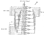
제6도의 데이타 코우드 변환부(4)의 1실시예가 제9도에 도시되어 있다. 제9도의 데이타 코우드 변환부(4)는 n1비트까지의 가변어장 데이타 코우드를 수신하기 위한 매트릭스형 회전회로(41), 회전회로(41)로부터 n1비트출력 신호를 수신하기 위한 제1레지스터회로(42), 제1선택회로(43), 제2선택회로(44), 제2레지스터회로(45), 제3레지스터회로(46) 및 상기회로 41내지 46을 제어하기 위한 제어회로(47)로 이루어진다.One embodiment of the
제1선택회로(43)는 제1레지스터회로(42)로부터 한 출력 데이타 신호를 받고, 제2레지스터회로(43)로부터 한 출력 데이타 신호를 받는다.The
제2선택회로(44)는 회전회로(41)로부터 한 출력 데이타 신호를 받고 제1선택회로(43)로부터 한 출력 데이타 신호를 받는다. 제2레지스터회로(45)는 제2선택회로(44)로부터 출력 데이타 신호를 받는다. 제3레지스터회로(46)는 제2레지스터회로(45)로부터 한 출력 데이타 신호를 받고 변환된 고정어장 데이타 코우드를 출력한다. 제어회로(47)는 어장정보신호 BN'1 내지 BN'm1과 클록신호(CLK')를 수신한다. 제9도의 데이타 코우드 변환부(4)의 동작은 제10도에 있어 입력 데이타 코우드의 일예를 참조하여 기술된다.The
데이타 코우드 변환부(4)는 8비트 구조를 갖고, 제10도에 도시된 가변어장 데이타 코우드 A내지 F는 차례로 제9도의 변환부(4) 내에 입력된다고 생각한다. 입력 데이타신호(S1)는 회전회로(41)에 있어 제어회로(47)로부터 제어신호에 의해 결정된 비트수에 의해 회전되며 회전회로(41)로부터의 회전된 데이타신호(S2)는 제1레지스터회로(42) 및 제6선택회로(44)에 공급된다. 예를 들면, 제1입력 데이타(A)는 회전됨이 없이 회전회로(41)로부터 출력한다.The
다음 데이타(A)는 신호 S2로서 제2선택회로(44)에 의해 출력하며 제2레지스터회로(45)내에 기입된다. 이 경우에 효과적인 데이타로서 6비트만이 제2레지스터회로(45)내에 기입되는 까닭에 유효한 6비트의 종단에 다음 입력 데이타(B)의 선도부의 2비트를 부착하는 것이 필요하다. 이에 따라 제2입력 데이타(B)는 8비트 데이타의 종단에 데이타(B)의 선도부의 2비트를 배열하기 위하여 회전회로(41)에서 회전된다. 이 회전된 데이타는 제1레지스터회로(42) 및 제2선택회로(44)에 공급된다. 이때 제2레지스터회로(45)로부터의 출력 데이타는 제1선택회로(43)에 의해 선택되어 제2선택회로(44)에 공급된다. 제2선택회로(44)에 있어서, 제1선택회로(44)에 있어서, 제1선택회로(43)부터의 데이타는 선도부의 6비트에 대해 선택되고 회전회로(41)로부터의 데이타는 남아 있는 2비트에 대해 선택되며, 제10도에 나타낸 바와 같이 결합된 8비트데이타는 제2선택회로(44)(S3로고)로부터 출력한다. 이 데이타(S3)는 제2레지스터회로(45) 내에 기입된다.The next data A is output by the
동시에 회전회로(41)로부터의 데이타(S2)는 제1레지스터회로(42) 내에 기입된다. 8비트 유현데이타는 제2레지스터회로(45) 내에 기입되기 때문에, 제2레지스터회로(45)로부터의 출력 데이타(S4)는 제어회로(47)로부터 클록신호에 의해 제3레지스터회로(46)에 기입되어 제1출력 데이타(A')로서 제3레지스터회로(46)로부터 출력한다.At the same time, the data S 2 from the
다음 제3입력 데이타(C)는 선행입력 데이타(B)의 남아 있는 1비트에 부착시키기 위하여 회전회로(41)에서 1비트만큼 회전된다. 이 경우에 데이타는 제1레지스터회로(42)에 남아 있어 제2레지스터회로(45) 내에는 기입되어 있지 않기 때문에 제1레지스터회로로(42)부터의 데이타 출력은 제1선택회로(43)에 의해 선택되어 제2선택회로(44)에 공급된다. 제2선택회로에 있어서, 제1선택회로로(43)부터의 데이타는 선도부의 1비트에 대해 선택되며 회전회로(41)로부터의 데이타(S1)는 남아 있는 7비트에 대해 선택된다.The third input data C is then rotated by one bit in the
제2선택회로(44)로부터 출력한 합성 데이타(S3)는 제2레지스터회로(45)에 공급되어 제2레지스터회로(45) 내에 기입된다. 유효의 8비트가 제2레지스터회로(45) 내에 기입되기 때문에, 제2레지스터회로(45)로 부터의 출력 데이타(S4)는 제3레지스터회로(46)내에 기입되어 제2출력 데이타(B')로서 제3레지스터회로(46)로부터 출력한다.The synthesis data S 3 output from the
다음 상기의 같은 동작이 반복된다. 즉 제2레지스터회로(45)에 기입되어 있지 않은 데이타 비트가 제1레지스터회로(42)에 남아있을 때, 새로운 입력 데이타는 남아 있는 비트의 종단에 부착되고 그 결합 데이타는 제2레지스터회로(45)에 기입된다.Then the same operation is repeated. That is, when data bits not written in the
제2레지스터회로(45)에 기입된 유효비트가 8비트가 아닐 때, 새로운 입력 데이타 제2레지스터회로(45)에 이미 기입된 데이타의 종단에 부착되며, 제2레지스터회로(45)에 기입된 유효비트가 8비트일 때 제2레지스터회로(45)로부터의 데이타 출력은 제3레지스터회로(46)에 기입되어 변환된 출력 데이타로서 제3레지스터회로(46)로부터 출력한다.When the valid bit written in the
상기 데이타 코우드 변환부(4)의 동작은 제어회로(47)의 제어하에 수행될 수 있다. 제어회로(47)는 제9도에 나타낸 바와 같이 구성될 수 있다. 제9도의 제어회로(47)는 가산기회로(471), 비트번호레지스(472) 디지탈 디지탈 변환기회로(473 및 474), 인버어터회로(475) 및 AND게이트회로(476)로 이루어진다. 어장정보 BN1내지 BNm은 가산기회로(471)에 공급되어 비트번호레지스터(472)의 출력에 가산된다.The operation of the
가산기회로(471)의 출력은 비트번호레지스터(472)에 공급되어 비트번호레지스터(472)에 기입된다. 비트번호레지스터(472)는 제2레지스터회로내에 기입된 유효비트. 번호를 나타내는 비트번호데이타와 8유효비트가 제2레지스터회로(45)에 기입되어 있는 것을 나타내는 "full"신호를 출력한다. 비트번호레지스터(472)로 부터의 비트번호데이타는 디지탈 디지탈 변환기회로(473 및 474)에 공급된다.The output of the adder circuit 471 is supplied to the
변환기회로(473 및 474)에 있어, 비트번호 데이타는 회전회로(41) 및 제2선택회로(44)에 대해 각각 제어신호로 변환된다. 회전회로(41)는 제11도와 같이 구성될 수 있다.In the
제11도의 회전회로(41)에 있어서 입력데이타비트 a1, a2, …a8은 제어회로(47)로부터의 제어신호(CNT)에 의해 결정된 비트수만큼 회전된다.In the
제9도에서 제1선택회로(43)는 제12도와 같이 구성될 수 있다. 제12도의 제1선택회로에 있어 제어회로(47)로부터의 푸울신호(FULL)가 논리 "low"였을 때 제2레지스터회로(45)로부터의 데이타는 제2선택회로(44)에 선택되어 출력한다. 제어회로(47)로부터의 푸울신호(FULL)가 논리 "high"였을 때 제1레지스터회로로부터의 데이타는 제2선택회로(44)에 선택되어 출력한다. 제9도에서 제2선택회로(44)는 제13도와 같이 구성될 수 있다. 제13도의 제2선택회로에서, 입력데이타의 각각의 비트에 대해서는, 제1선택회로(43)로부터의 데이타든가 또는 회전회로(41)로부터의 데이타인지의 선택은 제어회로(47)로부터의 제어신호 C1내지 C8에 의해 수행된다.In FIG. 9, the
제어신호 C1내지 C8은 제14도에 나타낸 바와 같이 제9도의 변환기회로(474)에 있는 비트번호 데이타에 따라 결정된다. 이에 따라, 제2선택회로(44)에 있어서, 제1선택회로(43)로부터의 데이타는 상단으로부터 레지스타(472)에 있는 비트번호까지의 비트에 대해 선택되며, 회전회로(41)로부터의 데이타는 남아 있는 비트에 대해서 선택된다. 제9도의 데이타 코우드변환부(4)에 따라 제어동작 및 제어회로는 상기 일본특허출원 번호 55-017,229에 기재된 데이타 코우드 변환회로와 비교하여 간단히 될 수 있다.The control signals C 1 to C 8 are determined according to the bit number data in the
Claims (2)
Applications Claiming Priority (2)
| Application Number | Priority Date | Filing Date | Title |
|---|---|---|---|
| JP111,445 | 1982-06-30 | ||
| JP57111445A JPS594255A (en) | 1982-06-30 | 1982-06-30 | Code converting circuit to variable length code |
Publications (2)
| Publication Number | Publication Date |
|---|---|
| KR840005290A KR840005290A (en) | 1984-11-05 |
| KR860001344B1 true KR860001344B1 (en) | 1986-09-15 |
Family
ID=14561377
Family Applications (1)
| Application Number | Title | Priority Date | Filing Date |
|---|---|---|---|
| KR1019830002965A KR860001344B1 (en) | 1982-06-30 | 1983-06-30 | Digital data code conversion circuit for variable word-length data code |
Country Status (2)
| Country | Link |
|---|---|
| JP (1) | JPS594255A (en) |
| KR (1) | KR860001344B1 (en) |
Families Citing this family (1)
| Publication number | Priority date | Publication date | Assignee | Title |
|---|---|---|---|---|
| JP4883301B2 (en) * | 2007-01-19 | 2012-02-22 | 井関農機株式会社 | Threshing device |
Family Cites Families (1)
| Publication number | Priority date | Publication date | Assignee | Title |
|---|---|---|---|---|
| JPS52105740A (en) * | 1976-03-01 | 1977-09-05 | Nippon Telegr & Teleph Corp <Ntt> | Buffer memory fead-out control system |
-
1982
- 1982-06-30 JP JP57111445A patent/JPS594255A/en active Granted
-
1983
- 1983-06-30 KR KR1019830002965A patent/KR860001344B1/en not_active IP Right Cessation
Also Published As
| Publication number | Publication date |
|---|---|
| JPS594255A (en) | 1984-01-11 |
| JPH0379889B2 (en) | 1991-12-20 |
| KR840005290A (en) | 1984-11-05 |
Similar Documents
| Publication | Publication Date | Title |
|---|---|---|
| US4593267A (en) | Digital data code conversion circuit for variable-word-length data code | |
| US5436626A (en) | Variable-length codeword encoder | |
| US4396906A (en) | Method and apparatus for digital Huffman encoding | |
| US5382955A (en) | Error tolerant thermometer-to-binary encoder | |
| EP0397686B1 (en) | Apparatus for efficiently packing data in a buffer | |
| EP0301191A2 (en) | PRML coding | |
| US4494151A (en) | 4-Pixel run-length code for data compression | |
| KR20000045256A (en) | Variable length coder of video coder and coding method using the same | |
| KR0178201B1 (en) | Variable length decoding apparatus | |
| JP2977570B2 (en) | Apparatus for implementing variable length encoding method and variable length decoding method | |
| EP0463216A1 (en) | Signal conversion circuit | |
| EP0467678A2 (en) | Variable length coding apparatus and variable length decoding apparatus | |
| US5309156A (en) | Variable-length code decoding device | |
| US20060187095A1 (en) | Method and apparatus for coding information, method and apparatus for decoding coded information, method of fabricating a recording medium, the recording medium and modulated signal | |
| GB1462889A (en) | Electrical encoding and decoding apparatus | |
| KR860001344B1 (en) | Digital data code conversion circuit for variable word-length data code | |
| US5736946A (en) | High speed apparatus and method for decoding variable length code | |
| US4486876A (en) | Broadband transmission on limited bandwidth digital line | |
| US5708430A (en) | High speed variable length code decoding apparatus | |
| US6639524B2 (en) | Method and apparatus for coding information, method and apparatus for decoding coded information, method of fabricating a recording medium, the recording medium and modulated signal | |
| EP0499225B1 (en) | Variable-length code decoding device | |
| KR100268831B1 (en) | High throughput variable length codec | |
| KR100275267B1 (en) | High speed variable length code decoding apparatus | |
| KR0121104B1 (en) | Variable length corder | |
| JP2712502B2 (en) | Transmission line encoding / decoding method |
Legal Events
| Date | Code | Title | Description |
|---|---|---|---|
| A201 | Request for examination | ||
| N231 | Notification of change of applicant | ||
| G160 | Decision to publish patent application | ||
| E701 | Decision to grant or registration of patent right | ||
| GRNT | Written decision to grant | ||
| FPAY | Annual fee payment |
Payment date: 20000906 Year of fee payment: 15 |
|
| LAPS | Lapse due to unpaid annual fee |