KR860000186B1 - Fm demoduating circuit - Google Patents
Fm demoduating circuit Download PDFInfo
- Publication number
- KR860000186B1 KR860000186B1 KR1019810002415A KR810002415A KR860000186B1 KR 860000186 B1 KR860000186 B1 KR 860000186B1 KR 1019810002415 A KR1019810002415 A KR 1019810002415A KR 810002415 A KR810002415 A KR 810002415A KR 860000186 B1 KR860000186 B1 KR 860000186B1
- Authority
- KR
- South Korea
- Prior art keywords
- circuit
- signal
- transistor
- output
- terminal
- Prior art date
Links
Images


Classifications
-
- H—ELECTRICITY
- H03—ELECTRONIC CIRCUITRY
- H03D—DEMODULATION OR TRANSFERENCE OF MODULATION FROM ONE CARRIER TO ANOTHER
- H03D3/00—Demodulation of angle-, frequency- or phase- modulated oscillations
- H03D3/02—Demodulation of angle-, frequency- or phase- modulated oscillations by detecting phase difference between two signals obtained from input signal
- H03D3/04—Demodulation of angle-, frequency- or phase- modulated oscillations by detecting phase difference between two signals obtained from input signal by counting or integrating cycles of oscillations
Abstract
Description
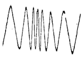
제1도는 종래의 펄스카운터 방식의 FM 복조회로의 회로도.1 is a circuit diagram of a conventional pulse counter type FM demodulation circuit.
제2(a)도 내지 제2(e)도는 제1도의 각부의 신호파형도.2 (a) to 2 (e) are signal waveform diagrams of respective parts of FIG.
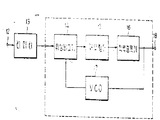
제3도는 PLL 방식의 FM 복조회로의 블록구성도.3 is a block diagram of the FM demodulation circuit of the PLL method.
제4도는 제3도의 복조출력 특성도.4 is a demodulation output characteristic diagram of FIG.
제5도는 제3도의 구체적 회로 구성을 표시하는 회로도.FIG. 5 is a circuit diagram showing a specific circuit configuration of FIG.
제6도는 본 발명에 관한 FM 복조 회로의 1실시예를 나타내는 회로도.6 is a circuit diagram showing one embodiment of an FM demodulation circuit according to the present invention.
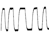
제7(a)도 내지 제7(f)도는 제6도의 동작을 설명하기 위한 신호 파형도이다.7 (a) to 7 (f) are signal waveform diagrams for explaining the operation of FIG.
본 발명은 예를 들어 텔레비젼 음성 다중신호의 반송부음성신호를 복조하는 데에 적합한 FM(주파수 변조) 복조회로에 관한 것이다.The present invention relates to an FM (frequency modulation) demodulation circuit suitable for demodulating, for example, a carrier audio signal of a television audio multiple signal.
일반적으로 텔레비젼 음성다중 신호의 부채널의 반송부음성신호(FM신호)를 복조하는 방식으로 펄스카운터 방식과 PLL (palse locked loop) 방식이 고려된다.In general, a pulse counter method and a PLL (palse locked loop) method are considered as a method of demodulating a subcarrier audio signal (FM signal) of a subchannel of a television audio multiple signal.
제1도는 펄스카운터 방식의 FM 복조회로의 1예를 표시하는 것으로서, 제2(a)도 내지 제2(e)도는 제1도에 표시하는 회로의 각부의 신호파형을 나타내는 것이다. 제2(a)도에 표시하는 것은 FM 신호이고, 동도면(b)에 표시하는 것은 이 FM 신호의 리미터(도시 생략) 출력이다. 이 리미터출력은 제1도에 표시하는 저항(R11)과 트랜스(11)의 코일(L11)에 의하여 미분되어 제2(e)도와 같은 파형이 된다. 이 미분신호는 다 이오드(D11), (D12)에 의하여 검파되어 제2(d)도와 같은 신호파형이 된다. 이 검파신호는 저항(R12)와 콘덴서(C11)로 구성되는 적분회로에 의하여 적분되어 제2(e)도와 같은 부음성신호로 변환된다. 또, (R13)은 저항이다.FIG. 1 shows an example of an FM demodulation circuit of the pulse counter method, and FIGS. 2 (a) to 2 (e) show signal waveforms of respective parts of the circuit shown in FIG. What is shown in FIG. 2 (a) is an FM signal, and what is shown in the same figure (b) is a limiter (not shown) output of this FM signal. The limiter output is differentiated by the resistor R 11 shown in FIG. 1 and the coil L 11 of the
그러나, 이러한 회로 구성에서는 코일(L11)을 사용하고 있으므로, 직적회로(IC)화에는 전적으로 부적당하다.However, in such a circuit configuration, since the coil L 11 is used, it is completely unsuitable for the formation of the direct circuit IC.
제3도는 PLL 방식의 FM 복조회로의 기본적 구성을 표시하는 것이다. 즉, (12)는 FM 신호의 입력단(13)은 리미터, (14)는 위상 비교기, (15)는 저역필터, (16)은 직류증폭기, (17)은 전압제어 발진기(VCO),(18)은 부음성신호의 출력단이다. 그리고, 위상 비교기(14), 저역필터(15), 직류증폭기(16), VCO (17)에 의하여 즉 FM 복조회로가 구성된다. 지금, PLL의 동작이 FM 신호에 동기하고 있다고 가정하면, VCO(17)의 발진주파수는 FM 신호의 순시주파수에 수반되어 변화한다. 이 VCO (17)은 저역필터(15)를 증폭한 것에 의하여 그 발진 주파수가 FM 신호의 주파수에 동기되도록 제어된다. 따라서 FM 신호의 주파수와 VCO (17) 의 제어전압간에는 제4도에 표시하는 바와 같은 FM 신호의 복조출력특성이 성립되어, 제어 전압 그 자체가 복조출력이 된다.3 shows the basic configuration of the FM demodulation circuit of the PLL method. In other words,
그러나, 이러한 PLL 방식의 FM 복조회로에서는 다음과 같은 결점이 있다.However, the PLL FM demodulation circuit has the following drawbacks.
(1) 포착범위 이상의 과변조 FM 신호가 들어갔을 경우, 복조 출력의 변형률이 대폭적으로 열화된다.(1) When an overmodulated FM signal that is larger than the capture range enters, the strain of the demodulation output is greatly degraded.
(2) PLL 자체가 대역 특성을 지니고 있으므로 복조회로에서 복조파가 지연되고 만다. 이로 인해 지연 시간을 보정하는 보정회로가 필요하다.(2) Since the PLL itself has band characteristics, the demodulation wave is delayed in the demodulation circuit. This requires a correction circuit to correct the delay time.
(3) VCO (17)의 자체 발진 주파수 조정이 필요하다.(3) Self-oscillation frequency adjustment of VCO 17 is necessary.
(4) 제5도의 구체적 회로에 표시하는 바와 같이 회로 구성이 복잡하고 소자수가 많다.(4) As shown in the specific circuit of FIG. 5, the circuit configuration is complicated and the number of elements is large.
이로 인해 소비전력의 증대 및 I C화 한 경우에 팁 면적이 증대하는 동시에 외부단자수, 주변부품수가 많아지는 결점이 있다. 또, 제5도에 있어서 제3도와 동일부는 동일부호를 단ㄷ. 도면에서 (Q11) 내지 (Q43)은 트랜지스터, (R15) 내지 (R35)는 저항(D13)(D14)는 다이오드, (C12), (C13)은 콘덴서, (Vcc)는 전원, (P11) 내지 (P14)는 외부단자이다. 외부단자(P11), (P14)에 접속된 콘덴서(C12), (C13)은 각각 발진용 콘덴서, 루우프 필터용 콘덴서이고, 외부단자(P12)에 접속된 저항(R35)는 발전 주파수 조정용의 가변저항이고, 외부단자(P31)은 복조신호의 출력단이다.As a result, in case of increasing power consumption and IC, the tip area increases, and the number of external terminals and peripheral parts increases. In Fig. 5, the same parts as in Fig. 3 are denoted by the same reference numerals. In the figure, (Q 11 ) to (Q 43 ) are transistors, (R 15 ) to (R 35 ) are resistors (D 13 ) (D 14 ) are diodes, (C 12 ), (C 13 ) are capacitors, (Vcc ) Is the power supply, and (P 11 ) to (P 14 ) are external terminals. The capacitors C 12 and C 13 connected to the external terminals P 11 and P 14 are oscillation capacitors and loop filter capacitors, respectively, and resistors R 35 connected to the external terminals P 12 . Is a variable resistor for generation frequency adjustment, and the external terminal P 31 is an output terminal of the demodulation signal.
본 발명은 상기의 사정에 대처하기 위하여 연구된 것으로서, I C화가 가능한 펄스카운터 방식의 호로 구성으로서 복조성능이 우수하고, 또 회로구성이 간단하고 소자수가 적고, 소비전력의 저감 및 I C 화에 있어서 팁면적이 축소, 외부단자수, 주변부품수의 감소를 도모할 수 있고, I C 화에 호적한 FM 복조회로를 제공하는 것을 목적으로 한다.The present invention has been studied in order to cope with the above situation, and has excellent demodulation performance, simple circuit configuration, small number of elements, and low power consumption. It is an object of the present invention to provide an FM demodulation circuit that can reduce the area, reduce the number of external terminals and the number of peripheral parts, and is suitable for IC.
이하, 도면을 참조하여 본 발명의 1 실시예를 상세히 설명한다. 제6도에서, (51)는 반송부음성 신호(FM 신호)의 입력단, (52)는 리미터이다. 이 리미터(52)의 한쪽의 출력단은 트랜지스터(Q51)의 베이스에 접속되고, 다른쪽의 출력단은 트랜지스터(Q52)의 베이스에 접속된다. 이 트랜지스터(Q51), (Q52)는 차동 증폭기를 구성하고, 그 에미터는 공통 접속되어서 전류원(I51)을 개재하여 기준전위단에 접속된다. 트랜지스터 (Q51), (Q52)의 콜렉터는 각각 저항(R51), (R52)를 개재하여 전원 Vcc에 접속되어 있다. 또 트랜지스터(Q51), (Q52)의 콜렉터간에는 다이오드(D51), (D52)가 각각 역방향으로 삽입된다. 또, 트랜지스터(Q52)의 콜렉터는 트랜지스터(Q53)의 베이스에 접속되고, 이 트랜지스터(Q53)의 콜렉터는 전원 Vcc에 접속되어 에미터는 전류원(I52)를 개재하여 기준 전위단에 접속되어 있다.Hereinafter, an embodiment of the present invention will be described in detail with reference to the drawings. In Fig. 6,
트랜지스터(Q53)의 에미터는 다시 저항(R53)을 개재하여 승산회로로서의 더블밸런스형 차동증폭기(53)을 구성하는 트랜지스터(Q54), (Q57)의 베이스에 접속되는 동시에 저항(R54)를 개재하여 트랜지스터(Q55), (Q56)의 베이스에 접속되고 있다. 이 트랜지스터(Q55), (Q56)의 베이스의 접속 중점에는 외부단자(P51)가 설치되고, 적분용 콘덴서(C51)이 접속되어 있다. 이 콘덴서(C51)과 저항(R54)에 의하여 적분회로가 구성된다. 더블밸랜스형 차동 증폭기(53)의 상단의 한쪽의 차동증폭기를 구성하는 트랜지스터 (Q54), (Q55)의 에미터는 공통 접속되어 트랜지스터(Q53)의 콜렉터에 접속되고, 이 트랜지스터(Q53)을 전류원으로 하고 있다. 다른쪽의 차동 증폭기를 구성하는 트랜지스터(Q56), (Q57)의 에미터도 공통 접속되어 트랜지스터(Q59)의 콜렉터에 접속되고, 이 트랜지스터(Q59)를 전류원으로 하고 있다. 이 한단의 차동 증폭기를 구성하는 트랜지스터(Q58), (Q59)의 에미터는 공통 접속되고, 전류원 I53을 개재하여 기준전위단에 접속되어 있다.The emitter of the transistor Q 53 is connected to the bases of the transistors Q 54 and Q 57 constituting the double balanced
트랜지스터(Q58)의 베이스에는 상기 리미터(52)의 한쪽의 출력단이 접속되고, 트랜지스터(Q59)의 베이스에는 다른쪽의 출력단이 접속되어 있다.One output terminal of the
상기 트랜지스터(Q54), (Q56)의 콜렉터는 공통 접속되어서 전원(Vcc)에 접속되어 있다. 상기 트랜지스터(Q55), (Q57)의 콜렉터도 공통 접속되어서 출력회로(54)의 커렌트미터 회로를 구성하는 트랜지스터(Q60)의 콜렉터에 접속되어 있다. 트랜지스터(Q60)의 에미터는 저항(R55)를 개재하여 전원(Vcc)에 접속되고, 베이스는 콜렉터와 단락되는 동시에 트랜지스터(Q61)의 베이스에 접속되어 있다. 트랜지스터(Q61)의 에미터는 저항(R56)을 개재하여 전원(Vcc)에 접속되고, 콜렉터는 저항(R57), (R58)을 개재하여 기준전위단에 접속되어 있다. 이 저항(R57), (R58)의 접속중점은 트랜지스터(Q62)의 베이스에 접속되고, 이 트랜지스터(Q62)의 에미터는 기준전위단에 접속되고, 콜렉터는 저항(R59)를 개재하여 전원(Vcc)에 접속되는 동시에 트랜지스터(Q63)의 베이스에 접속되어 있다. 이 트랜지스터(Q63)의 콜렉터는 전원(Vcc)에 접속되고, 에미터는 저항(R60)을 개재하여 기준전위단에 접속되는 동시에 외부단자(P52)에 접속되어 있다. 이 단자(P52)에는 로우패스필터(LPF)(55)가 접속되어 있다.The collectors of the transistors Q 54 and Q 56 are connected in common and are connected to a power supply Vcc. The collectors of the transistors Q 55 and Q 57 are also commonly connected and connected to the collector of the transistor Q 60 constituting the current meter circuit of the
상기 구성에서 제7(a)도 내지 제7(f)도의 신호 파형도를 참조하면서 동작을 설명한다. 반송부음성 신호(F M 신호)는 리미터(52)에 의하여 충분히 진폭제한 작용을 받아서 제7(a)도에 표시하는 바와 같은 신호로 변환되어 트랜지스터(Q51), (Q52) 및 (Q58), (Q59)의 베이스에 공급된다. 트랜지스터(Q51), (Q52)의 베이스에 공급된 리미터 출력은 트랜지스터(Q52)의 콜렉터에서 에미터폴로 워구성의 트랜지스터(Q53)에 공급된다. 그리고, 이 트랜지스터(Q53)의 에미터에서 저항(R53)을 개재하여 트랜지스터(Q54), (Q57)의 베이스에 공급되는 동시에 저항(R54)를 개재하여 트랜지스터(Q55), (Q56)의 베이스에 공급된다. 트랜지스터 (Q54), (Q57)의 베이스에는 제7(b)도에서 표시하는 바와 같이 리미터 출력이 대략 그대로의 상태로 공급된다. 한편 트랜지스터(Q55), (Q56)의 베이스에 공급되는 신호는 저항(R54)와 콘덴서(C51)로 구성되는 적분 회로에 의하여 적분되어 제7(c)도에서 표시하는 바와 같은 신호로서 공급된다. 이로 인해, 트랜지스터(Q55), (Q56)의 베이스에 공급되는 신호는 트랜지스터(Q54), (Q57)의 베이스에 공급되는 신호에 대하여 시간 지연이 생기게 된다. 이러한 결과로, 더블밸런스형 차동증폭기(53)의 트랜지스터(Q55), (Q57)의 콜렉터에는 상기 시간 지연에 따르는 양 신호의 차분(差分)이 취출 된다. 이 더블밸런스형 창등증폭기(53)의 출력신호를 제7(b)도에 표시한다. 이 출력신호는 트랜지스터(Q60), (Q61), (Q62)에 의하여 펄스 증폭되어 에미터 플로워구성의 트랜지스터(Q63)의 에미터에 제7(e)도에 표시하는 바와 같은 펄스신호로서 도출된다. 이 펄스신호는 LPF(55)에 의하여 적분되어 제7(f)도에서 보는 바와 같은 부음성 신호로서 복조된다.The operation will be described with reference to the signal waveform diagrams of Figs. 7 (a) to 7 (f) in the above configuration. The carrier negative signal (FM signal) is sufficiently limited by the
또, 부음성신호의 복조출력레벨은 저항(R54)와 콘덴서(C51)에 의하여 결정되는 적분시정수를 적절히 설정함으로서, 최적레벨로 조정할 수 있다.The demodulation output level of the negative audio signal can be adjusted to an optimum level by appropriately setting the integral time constant determined by the resistor R 54 and the capacitor C 51 .
이상 상세하게 설명한 본 실시에에 의하여 회로의 대부분이 트랜지스터나 저항 등과 같은 I C 화에 적당한 소자에 의하여 구성되어 있으므로 종래 기술에서는 I C 화가 어렵다고 생각하던 펄스카운트 방식의 FM 복조회로의 I C 화를 실행할 수 있다. 또, 펄스카운트 방식을 책용하고 있기 때문에 복조성능이 우수하고, 고품위의 부음성신호를 얻을 수가 있다. 또 회로구성이 간단하고 소자수가 적어진다. 회로의 소비전력의 저감 및 I C화된 경우에 팁면적의 축소를 도모할 수 있음을 물론이고, 외부단자나 주변부품도 적고 I C 화에 대단히 편리하다.According to the present embodiment described in detail above, since most of the circuits are constituted by devices suitable for ICs such as transistors and resistors, ICs of the pulse count type FM demodulation circuit, which is considered difficult to IC in the prior art, can be implemented. have. In addition, since the pulse count method is used, demodulation performance is excellent and a high quality negative audio signal can be obtained. In addition, the circuit configuration is simple and the number of elements is small. It is possible to reduce the power consumption of the circuit and to reduce the tip area in the case of IC, and there are few external terminals and peripheral parts, and it is very convenient for IC.
또, 전원라인(L51)로 부터의 리플은 전류 미터회로의 트랜지스터(Q60), (Q61)의 에미터전류에 동상(同相)에서 발생하여 이 트랜지스터(Q60), (Q61)의 베이스에서 사라진다. 따라서 더블랜런스형 차동증폭기(53)의 출력전원 리플이 편승하는 일은 없고, 부음성 신호의 복조출력이 전원리플에 의하여 악영향을 받은 일이 없다.In addition, the power supply line ripple from the (L 51) is a current meter circuit transistor (Q 60), a transistor (Q 60), (Q 61 ) is generated in the statue (同相) to the emitter current of the (Q 61) of the Disappears from its base. Therefore, the output power supply ripple of the double-
또, 본 발명은 상기의 실시예에 하정되는 것은 아니다. 예를 들면 트랜지스터(Q55), (Q56)의 베이스 입력으로는 리미터출력을 적분한 것에 한정되지 않고, 리미터출력을 지연회로를 통해서 소정시간 지연시킨 것을 사용해도 좋은 것은 물론이다. 이와 같은 구성에 의하면, 트랜지스터(Q60), (Q61), (Q62) 등으로 구성되는 더블밸런스형 차동증폭기(53) 출력은 펄스상으로 변환하기 위한 회로가 필요 없어지는 이점이 있다. 또, 상기 실시예에 있어서 더블밸런스형 차동증폭기(53) 출력을 직접LPF(55)에 공급하도록 해도 된다. 또, 승산회로로서는 더블밸런스형 차동증폭기(53)에 한정되지 않고, I C 화에 적합한 소자로 구성되는 것이면 다른 주지의 회로라도 좋다. 또 본 발명의 FM 복조회로는 텔레비젼 음성다중신호의 반송부음성신호의 복조만 아니라, 다른 신호의 복조에도 적용이 가능함은 물론이다.In addition, this invention is not limited to the said Example. For example, the base inputs of the transistors Q 55 and Q 56 are not limited to the ones in which the limiter outputs are integrated, but of course, a delayed predetermined time limiter output may be used. With this configuration, transistor (Q 60), (Q 61), (Q 62), a double-balanced differential amplifier (53) consisting of light output has the circuit has stopped requires an advantage for converting the phase pulse. In the above embodiment, the output of the double balanced
이와 같이 본 발명에 의하면 I C 화가 가능한 펄스카운트 방식의 회로구성으로서 복조성능이 우수하고, 또 회로구성이 간단하고 소자수가 적고, 소비 전력의 저감 및 I C화에 있어서 팁 면적의 축소, 외부단자수, 주변부품수의 감소를 도모할 수 있고, I C화에 적합한 FM 복조회로를 제공할 수 있다.As described above, according to the present invention, the circuit configuration of the pulse count method that can be IC is excellent, the demodulation performance is excellent, the circuit configuration is simple, the number of elements is small, the reduction of the tip area, the number of external terminals, The number of peripheral components can be reduced, and an FM demodulation circuit suitable for IC can be provided.
Claims (1)
Applications Claiming Priority (2)
| Application Number | Priority Date | Filing Date | Title |
|---|---|---|---|
| JP9094080A JPS5715505A (en) | 1980-07-03 | 1980-07-03 | Fm demodulation circuit |
| JP90940 | 1980-07-03 |
Publications (2)
| Publication Number | Publication Date |
|---|---|
| KR830006983A KR830006983A (en) | 1983-10-12 |
| KR860000186B1 true KR860000186B1 (en) | 1986-02-28 |
Family
ID=14012442
Family Applications (1)
| Application Number | Title | Priority Date | Filing Date |
|---|---|---|---|
| KR1019810002415A KR860000186B1 (en) | 1980-07-03 | 1981-07-03 | Fm demoduating circuit |
Country Status (5)
| Country | Link |
|---|---|
| US (1) | US4511849A (en) |
| JP (1) | JPS5715505A (en) |
| KR (1) | KR860000186B1 (en) |
| DE (1) | DE3125825C2 (en) |
| GB (1) | GB2079076B (en) |
Families Citing this family (8)
| Publication number | Priority date | Publication date | Assignee | Title |
|---|---|---|---|---|
| JPS61171322U (en) * | 1985-04-12 | 1986-10-24 | ||
| JPH0659010B2 (en) * | 1985-12-18 | 1994-08-03 | 株式会社日立製作所 | FM signal demodulator |
| EP0289346B1 (en) * | 1987-04-30 | 1995-08-16 | Matsushita Electric Industrial Co., Ltd. | Frequency demodulation circuit |
| JPH083939B2 (en) * | 1988-09-19 | 1996-01-17 | 松下電器産業株式会社 | FM demodulation circuit |
| IL89259A0 (en) * | 1989-02-10 | 1989-09-10 | Avr Communications Ltd | Audio apparatus |
| JPH04134929A (en) * | 1990-09-26 | 1992-05-08 | Pioneer Electron Corp | Multi-path detector |
| TW257917B (en) * | 1994-04-12 | 1995-09-21 | Philips Electronics Nv | Receiver comprising a pulse count FM demodulator, and pulse count FM demodulator |
| JPH09172584A (en) * | 1995-12-20 | 1997-06-30 | Rohm Co Ltd | Sif signal processing circuit |
Family Cites Families (11)
| Publication number | Priority date | Publication date | Assignee | Title |
|---|---|---|---|---|
| JPS4979719A (en) * | 1972-12-08 | 1974-08-01 | ||
| JPS5639565B2 (en) * | 1972-12-21 | 1981-09-14 | ||
| JPS5233460A (en) * | 1975-09-10 | 1977-03-14 | Sony Corp | Fm demodulator |
| JPS52149907A (en) * | 1976-06-09 | 1977-12-13 | Hitachi Ltd | Intra-office noise reducing device of fm receiver |
| JPS5328361A (en) * | 1976-08-27 | 1978-03-16 | Sony Corp | Quadratur e phase detection circuit |
| EP0003393B1 (en) * | 1978-01-18 | 1982-06-23 | Rca Corporation | Chroma demodulator circuit for secam television signals |
| JPS54101651A (en) * | 1978-01-27 | 1979-08-10 | Toshiba Corp | Fm demodulator circuit |
| JPS54161260A (en) * | 1978-06-09 | 1979-12-20 | Sanyo Electric Co Ltd | Fm demodulation circuit |
| US4342000A (en) * | 1979-04-04 | 1982-07-27 | Nippon Gakki Seizo Kabushiki Kaisha | FM Detecting circuit |
| JPS55158733A (en) * | 1979-05-29 | 1980-12-10 | Toshiba Corp | Delay type fm demodulating circuit |
| US4280100A (en) * | 1979-09-20 | 1981-07-21 | Bell & Howell Company | Time modulation pulse averaging demodulator |
-
1980
- 1980-07-03 JP JP9094080A patent/JPS5715505A/en active Granted
-
1981
- 1981-06-29 GB GB8119947A patent/GB2079076B/en not_active Expired
- 1981-06-30 US US06/279,078 patent/US4511849A/en not_active Expired - Lifetime
- 1981-07-01 DE DE3125825A patent/DE3125825C2/en not_active Expired
- 1981-07-03 KR KR1019810002415A patent/KR860000186B1/en active
Also Published As
| Publication number | Publication date |
|---|---|
| KR830006983A (en) | 1983-10-12 |
| GB2079076B (en) | 1984-11-21 |
| DE3125825A1 (en) | 1982-04-08 |
| US4511849A (en) | 1985-04-16 |
| DE3125825C2 (en) | 1985-09-26 |
| JPS5715505A (en) | 1982-01-26 |
| GB2079076A (en) | 1982-01-13 |
| JPS6236401B2 (en) | 1987-08-06 |
Similar Documents
| Publication | Publication Date | Title |
|---|---|---|
| KR900002955B1 (en) | Auto control circuit of filter circuit's time constant | |
| EP0196697A1 (en) | AM receiver | |
| KR0146287B1 (en) | Monostable multivibrator | |
| US5896053A (en) | Single ended to differential converter and 50% duty cycle signal generator and method | |
| US5650749A (en) | FM demodulator using injection locked oscillator having tuning feedback and linearizing feedback | |
| KR860000186B1 (en) | Fm demoduating circuit | |
| JP4006380B2 (en) | Frequency generation circuit and communication system | |
| US4005476A (en) | Circuit for compensating time errors in a television signal, particularly from a recording instrument | |
| KR890004160B1 (en) | Fm detecting system of automatic tuning phase synchronous loop | |
| US3783304A (en) | Constant pulse width generator | |
| US4275417A (en) | Aperture correction signal processing circuit | |
| US3764925A (en) | Demodulator circuit | |
| JPH0336099Y2 (en) | ||
| JP3479334B2 (en) | Circuit for stereo and dual audio signal recognition | |
| US4471311A (en) | Detector circuit having AGC function | |
| US3918014A (en) | Gyrator resonant circuit having regulation of supply current | |
| JP2530229B2 (en) | Video signal clamp circuit | |
| US6618448B1 (en) | DC recovery circuit capable of receiving ECL signal even under low power supply voltage | |
| JP2684837B2 (en) | Differential amplifier circuit | |
| JPS60134607A (en) | Oscillator circuit | |
| US2965848A (en) | Detector circuit arrangement | |
| US4620314A (en) | Method of generating an approximately sinusoidal signal and circuit arrangement for implementing this method, particularly in a stereo demodulator | |
| JPS61147611A (en) | Agc circuit | |
| JPS6327455Y2 (en) | ||
| GB2144939A (en) | Receiver including surface acoustic wave amplifier |