KR20230132474A - Display devices and electronic devices - Google Patents
Display devices and electronic devices Download PDFInfo
- Publication number
- KR20230132474A KR20230132474A KR1020237024489A KR20237024489A KR20230132474A KR 20230132474 A KR20230132474 A KR 20230132474A KR 1020237024489 A KR1020237024489 A KR 1020237024489A KR 20237024489 A KR20237024489 A KR 20237024489A KR 20230132474 A KR20230132474 A KR 20230132474A
- Authority
- KR
- South Korea
- Prior art keywords
- wiring
- pixel
- circuit
- area
- display device
- Prior art date
Links
- 239000004065 semiconductor Substances 0.000 claims description 142
- 238000000034 method Methods 0.000 claims description 90
- 239000000758 substrate Substances 0.000 claims description 87
- 229910044991 metal oxide Inorganic materials 0.000 claims description 53
- 150000004706 metal oxides Chemical class 0.000 claims description 53
- 230000015572 biosynthetic process Effects 0.000 claims description 49
- 229910052710 silicon Inorganic materials 0.000 claims description 46
- 239000010703 silicon Substances 0.000 claims description 46
- 239000011159 matrix material Substances 0.000 claims description 29
- 230000005540 biological transmission Effects 0.000 claims description 10
- 239000012212 insulator Substances 0.000 description 603
- 239000010410 layer Substances 0.000 description 405
- 239000004020 conductor Substances 0.000 description 365
- 239000010408 film Substances 0.000 description 170
- 230000006870 function Effects 0.000 description 156
- 229910052760 oxygen Inorganic materials 0.000 description 135
- 239000001301 oxygen Substances 0.000 description 132
- QVGXLLKOCUKJST-UHFFFAOYSA-N atomic oxygen Chemical compound [O] QVGXLLKOCUKJST-UHFFFAOYSA-N 0.000 description 130
- 229910052739 hydrogen Inorganic materials 0.000 description 103
- 239000001257 hydrogen Substances 0.000 description 103
- UFHFLCQGNIYNRP-UHFFFAOYSA-N Hydrogen Chemical compound [H][H] UFHFLCQGNIYNRP-UHFFFAOYSA-N 0.000 description 84
- 238000005401 electroluminescence Methods 0.000 description 84
- 239000000463 material Substances 0.000 description 76
- 239000012535 impurity Substances 0.000 description 74
- 101100270422 Rattus norvegicus Arhgef7 gene Proteins 0.000 description 73
- 238000010586 diagram Methods 0.000 description 62
- IJGRMHOSHXDMSA-UHFFFAOYSA-N Atomic nitrogen Chemical compound N#N IJGRMHOSHXDMSA-UHFFFAOYSA-N 0.000 description 55
- 239000007789 gas Substances 0.000 description 49
- 239000013078 crystal Substances 0.000 description 44
- XUIMIQQOPSSXEZ-UHFFFAOYSA-N Silicon Chemical compound [Si] XUIMIQQOPSSXEZ-UHFFFAOYSA-N 0.000 description 43
- 238000009792 diffusion process Methods 0.000 description 41
- 229910052581 Si3N4 Inorganic materials 0.000 description 34
- HQVNEWCFYHHQES-UHFFFAOYSA-N silicon nitride Chemical compound N12[Si]34N5[Si]62N3[Si]51N64 HQVNEWCFYHHQES-UHFFFAOYSA-N 0.000 description 34
- 230000004888 barrier function Effects 0.000 description 33
- 239000011701 zinc Substances 0.000 description 33
- 229910052751 metal Inorganic materials 0.000 description 29
- 229910052782 aluminium Inorganic materials 0.000 description 27
- XLYOFNOQVPJJNP-UHFFFAOYSA-N water Substances O XLYOFNOQVPJJNP-UHFFFAOYSA-N 0.000 description 27
- XAGFODPZIPBFFR-UHFFFAOYSA-N aluminium Chemical compound [Al] XAGFODPZIPBFFR-UHFFFAOYSA-N 0.000 description 26
- 229910052757 nitrogen Inorganic materials 0.000 description 26
- TWNQGVIAIRXVLR-UHFFFAOYSA-N oxo(oxoalumanyloxy)alumane Chemical compound O=[Al]O[Al]=O TWNQGVIAIRXVLR-UHFFFAOYSA-N 0.000 description 26
- VYPSYNLAJGMNEJ-UHFFFAOYSA-N silicon dioxide Inorganic materials O=[Si]=O VYPSYNLAJGMNEJ-UHFFFAOYSA-N 0.000 description 25
- 230000001965 increasing effect Effects 0.000 description 24
- 229910052814 silicon oxide Inorganic materials 0.000 description 24
- 239000003086 colorant Substances 0.000 description 23
- 239000002184 metal Substances 0.000 description 23
- 125000004429 atom Chemical group 0.000 description 22
- 229910052735 hafnium Inorganic materials 0.000 description 22
- 239000000203 mixture Substances 0.000 description 21
- 238000006243 chemical reaction Methods 0.000 description 20
- 239000012790 adhesive layer Substances 0.000 description 19
- 238000000231 atomic layer deposition Methods 0.000 description 19
- 230000007547 defect Effects 0.000 description 19
- 150000002431 hydrogen Chemical class 0.000 description 19
- 238000010438 heat treatment Methods 0.000 description 17
- 238000004519 manufacturing process Methods 0.000 description 17
- WFKWXMTUELFFGS-UHFFFAOYSA-N tungsten Chemical compound [W] WFKWXMTUELFFGS-UHFFFAOYSA-N 0.000 description 17
- 229910052721 tungsten Inorganic materials 0.000 description 17
- 239000010937 tungsten Substances 0.000 description 17
- VBJZVLUMGGDVMO-UHFFFAOYSA-N hafnium atom Chemical compound [Hf] VBJZVLUMGGDVMO-UHFFFAOYSA-N 0.000 description 16
- 230000003071 parasitic effect Effects 0.000 description 16
- 230000007423 decrease Effects 0.000 description 15
- -1 polyethylene terephthalate Polymers 0.000 description 15
- 239000002994 raw material Substances 0.000 description 15
- 239000011347 resin Substances 0.000 description 15
- 229920005989 resin Polymers 0.000 description 15
- 210000001508 eye Anatomy 0.000 description 14
- 239000002243 precursor Substances 0.000 description 13
- MWUXSHHQAYIFBG-UHFFFAOYSA-N Nitric oxide Chemical compound O=[N] MWUXSHHQAYIFBG-UHFFFAOYSA-N 0.000 description 12
- 239000012298 atmosphere Substances 0.000 description 12
- 230000000694 effects Effects 0.000 description 12
- 238000012545 processing Methods 0.000 description 12
- 239000002356 single layer Substances 0.000 description 12
- 229910052719 titanium Inorganic materials 0.000 description 12
- 239000010936 titanium Chemical group 0.000 description 12
- 229910052738 indium Inorganic materials 0.000 description 11
- 239000011261 inert gas Substances 0.000 description 11
- 150000004767 nitrides Chemical class 0.000 description 11
- OKTJSMMVPCPJKN-UHFFFAOYSA-N Carbon Chemical compound [C] OKTJSMMVPCPJKN-UHFFFAOYSA-N 0.000 description 10
- RYGMFSIKBFXOCR-UHFFFAOYSA-N Copper Chemical group [Cu] RYGMFSIKBFXOCR-UHFFFAOYSA-N 0.000 description 10
- PXHVJJICTQNCMI-UHFFFAOYSA-N Nickel Chemical group [Ni] PXHVJJICTQNCMI-UHFFFAOYSA-N 0.000 description 10
- RTAQQCXQSZGOHL-UHFFFAOYSA-N Titanium Chemical group [Ti] RTAQQCXQSZGOHL-UHFFFAOYSA-N 0.000 description 10
- 229910052799 carbon Inorganic materials 0.000 description 10
- 239000000969 carrier Substances 0.000 description 10
- 230000008859 change Effects 0.000 description 10
- 239000010409 thin film Substances 0.000 description 10
- 238000002441 X-ray diffraction Methods 0.000 description 9
- 230000003321 amplification Effects 0.000 description 9
- 238000005229 chemical vapour deposition Methods 0.000 description 9
- APFVFJFRJDLVQX-UHFFFAOYSA-N indium atom Chemical compound [In] APFVFJFRJDLVQX-UHFFFAOYSA-N 0.000 description 9
- 238000002347 injection Methods 0.000 description 9
- 239000007924 injection Substances 0.000 description 9
- 238000003199 nucleic acid amplification method Methods 0.000 description 9
- 229910052715 tantalum Inorganic materials 0.000 description 9
- GUVRBAGPIYLISA-UHFFFAOYSA-N tantalum atom Chemical compound [Ta] GUVRBAGPIYLISA-UHFFFAOYSA-N 0.000 description 9
- 230000005669 field effect Effects 0.000 description 8
- 229910052733 gallium Inorganic materials 0.000 description 8
- 229910000449 hafnium oxide Inorganic materials 0.000 description 8
- WIHZLLGSGQNAGK-UHFFFAOYSA-N hafnium(4+);oxygen(2-) Chemical compound [O-2].[O-2].[Hf+4] WIHZLLGSGQNAGK-UHFFFAOYSA-N 0.000 description 8
- 229910010272 inorganic material Inorganic materials 0.000 description 8
- 239000011229 interlayer Substances 0.000 description 8
- CPLXHLVBOLITMK-UHFFFAOYSA-N magnesium oxide Inorganic materials [Mg]=O CPLXHLVBOLITMK-UHFFFAOYSA-N 0.000 description 8
- 239000007800 oxidant agent Substances 0.000 description 8
- 125000004430 oxygen atom Chemical group O* 0.000 description 8
- 238000004544 sputter deposition Methods 0.000 description 8
- 239000010949 copper Substances 0.000 description 7
- PMHQVHHXPFUNSP-UHFFFAOYSA-M copper(1+);methylsulfanylmethane;bromide Chemical compound Br[Cu].CSC PMHQVHHXPFUNSP-UHFFFAOYSA-M 0.000 description 7
- 238000002003 electron diffraction Methods 0.000 description 7
- 239000011147 inorganic material Substances 0.000 description 7
- 239000000395 magnesium oxide Substances 0.000 description 7
- 230000003647 oxidation Effects 0.000 description 7
- 238000007254 oxidation reaction Methods 0.000 description 7
- 230000008569 process Effects 0.000 description 7
- 239000002096 quantum dot Substances 0.000 description 7
- 238000001228 spectrum Methods 0.000 description 7
- MZLGASXMSKOWSE-UHFFFAOYSA-N tantalum nitride Chemical compound [Ta]#N MZLGASXMSKOWSE-UHFFFAOYSA-N 0.000 description 7
- 229910052720 vanadium Inorganic materials 0.000 description 7
- XLOMVQKBTHCTTD-UHFFFAOYSA-N zinc oxide Inorganic materials [Zn]=O XLOMVQKBTHCTTD-UHFFFAOYSA-N 0.000 description 7
- GYHNNYVSQQEPJS-UHFFFAOYSA-N Gallium Chemical group [Ga] GYHNNYVSQQEPJS-UHFFFAOYSA-N 0.000 description 6
- XEEYBQQBJWHFJM-UHFFFAOYSA-N Iron Chemical group [Fe] XEEYBQQBJWHFJM-UHFFFAOYSA-N 0.000 description 6
- NRTOMJZYCJJWKI-UHFFFAOYSA-N Titanium nitride Chemical compound [Ti]#N NRTOMJZYCJJWKI-UHFFFAOYSA-N 0.000 description 6
- 229910052784 alkaline earth metal Inorganic materials 0.000 description 6
- 150000001875 compounds Chemical class 0.000 description 6
- 229910052802 copper Inorganic materials 0.000 description 6
- 230000005684 electric field Effects 0.000 description 6
- 125000004435 hydrogen atom Chemical group [H]* 0.000 description 6
- 239000011810 insulating material Substances 0.000 description 6
- 238000002955 isolation Methods 0.000 description 6
- AXZKOIWUVFPNLO-UHFFFAOYSA-N magnesium;oxygen(2-) Chemical compound [O-2].[Mg+2] AXZKOIWUVFPNLO-UHFFFAOYSA-N 0.000 description 6
- 230000003287 optical effect Effects 0.000 description 6
- 239000011368 organic material Substances 0.000 description 6
- 238000000206 photolithography Methods 0.000 description 6
- 238000007639 printing Methods 0.000 description 6
- 238000007789 sealing Methods 0.000 description 6
- 238000013461 design Methods 0.000 description 5
- 230000006872 improvement Effects 0.000 description 5
- 239000007788 liquid Substances 0.000 description 5
- 239000002159 nanocrystal Substances 0.000 description 5
- 229910052759 nickel Inorganic materials 0.000 description 5
- 230000001590 oxidative effect Effects 0.000 description 5
- 230000035515 penetration Effects 0.000 description 5
- 229910052707 ruthenium Inorganic materials 0.000 description 5
- 238000001004 secondary ion mass spectrometry Methods 0.000 description 5
- 238000002230 thermal chemical vapour deposition Methods 0.000 description 5
- 229910052725 zinc Inorganic materials 0.000 description 5
- XKRFYHLGVUSROY-UHFFFAOYSA-N Argon Chemical compound [Ar] XKRFYHLGVUSROY-UHFFFAOYSA-N 0.000 description 4
- ZOXJGFHDIHLPTG-UHFFFAOYSA-N Boron Chemical compound [B] ZOXJGFHDIHLPTG-UHFFFAOYSA-N 0.000 description 4
- ZOKXTWBITQBERF-UHFFFAOYSA-N Molybdenum Chemical compound [Mo] ZOKXTWBITQBERF-UHFFFAOYSA-N 0.000 description 4
- 239000004642 Polyimide Substances 0.000 description 4
- KJTLSVCANCCWHF-UHFFFAOYSA-N Ruthenium Chemical compound [Ru] KJTLSVCANCCWHF-UHFFFAOYSA-N 0.000 description 4
- BQCADISMDOOEFD-UHFFFAOYSA-N Silver Chemical compound [Ag] BQCADISMDOOEFD-UHFFFAOYSA-N 0.000 description 4
- 229910007541 Zn O Inorganic materials 0.000 description 4
- 229910052783 alkali metal Inorganic materials 0.000 description 4
- 150000001340 alkali metals Chemical class 0.000 description 4
- 150000001342 alkaline earth metals Chemical class 0.000 description 4
- 229910052796 boron Inorganic materials 0.000 description 4
- 238000000576 coating method Methods 0.000 description 4
- 230000000295 complement effect Effects 0.000 description 4
- 238000010894 electron beam technology Methods 0.000 description 4
- 238000002524 electron diffraction data Methods 0.000 description 4
- 229910052732 germanium Inorganic materials 0.000 description 4
- GNPVGFCGXDBREM-UHFFFAOYSA-N germanium atom Chemical compound [Ge] GNPVGFCGXDBREM-UHFFFAOYSA-N 0.000 description 4
- 210000003128 head Anatomy 0.000 description 4
- 230000005525 hole transport Effects 0.000 description 4
- 238000007654 immersion Methods 0.000 description 4
- 229910003437 indium oxide Inorganic materials 0.000 description 4
- PJXISJQVUVHSOJ-UHFFFAOYSA-N indium(iii) oxide Chemical compound [O-2].[O-2].[O-2].[In+3].[In+3] PJXISJQVUVHSOJ-UHFFFAOYSA-N 0.000 description 4
- AMGQUBHHOARCQH-UHFFFAOYSA-N indium;oxotin Chemical compound [In].[Sn]=O AMGQUBHHOARCQH-UHFFFAOYSA-N 0.000 description 4
- 230000007246 mechanism Effects 0.000 description 4
- 229910052750 molybdenum Inorganic materials 0.000 description 4
- 239000011733 molybdenum Substances 0.000 description 4
- 229920001721 polyimide Polymers 0.000 description 4
- 229910001925 ruthenium oxide Inorganic materials 0.000 description 4
- WOCIAKWEIIZHES-UHFFFAOYSA-N ruthenium(iv) oxide Chemical compound O=[Ru]=O WOCIAKWEIIZHES-UHFFFAOYSA-N 0.000 description 4
- 239000000523 sample Substances 0.000 description 4
- 229910052709 silver Inorganic materials 0.000 description 4
- 239000004332 silver Substances 0.000 description 4
- 239000000126 substance Substances 0.000 description 4
- 239000011787 zinc oxide Substances 0.000 description 4
- 239000004925 Acrylic resin Substances 0.000 description 3
- 229920000178 Acrylic resin Polymers 0.000 description 3
- JBRZTFJDHDCESZ-UHFFFAOYSA-N AsGa Chemical compound [As]#[Ga] JBRZTFJDHDCESZ-UHFFFAOYSA-N 0.000 description 3
- YCKRFDGAMUMZLT-UHFFFAOYSA-N Fluorine atom Chemical compound [F] YCKRFDGAMUMZLT-UHFFFAOYSA-N 0.000 description 3
- 229910001218 Gallium arsenide Inorganic materials 0.000 description 3
- FYYHWMGAXLPEAU-UHFFFAOYSA-N Magnesium Chemical compound [Mg] FYYHWMGAXLPEAU-UHFFFAOYSA-N 0.000 description 3
- KDLHZDBZIXYQEI-UHFFFAOYSA-N Palladium Chemical compound [Pd] KDLHZDBZIXYQEI-UHFFFAOYSA-N 0.000 description 3
- ATJFFYVFTNAWJD-UHFFFAOYSA-N Tin Chemical group [Sn] ATJFFYVFTNAWJD-UHFFFAOYSA-N 0.000 description 3
- HCHKCACWOHOZIP-UHFFFAOYSA-N Zinc Chemical compound [Zn] HCHKCACWOHOZIP-UHFFFAOYSA-N 0.000 description 3
- 239000000956 alloy Substances 0.000 description 3
- 239000003795 chemical substances by application Substances 0.000 description 3
- 238000012937 correction Methods 0.000 description 3
- 238000000151 deposition Methods 0.000 description 3
- AJNVQOSZGJRYEI-UHFFFAOYSA-N digallium;oxygen(2-) Chemical compound [O-2].[O-2].[O-2].[Ga+3].[Ga+3] AJNVQOSZGJRYEI-UHFFFAOYSA-N 0.000 description 3
- 229910001873 dinitrogen Inorganic materials 0.000 description 3
- 238000002149 energy-dispersive X-ray emission spectroscopy Methods 0.000 description 3
- 239000011737 fluorine Substances 0.000 description 3
- 229910052731 fluorine Inorganic materials 0.000 description 3
- 229910001195 gallium oxide Inorganic materials 0.000 description 3
- 239000011521 glass Substances 0.000 description 3
- 150000002500 ions Chemical class 0.000 description 3
- 229910052742 iron Inorganic materials 0.000 description 3
- 229910052746 lanthanum Inorganic materials 0.000 description 3
- FZLIPJUXYLNCLC-UHFFFAOYSA-N lanthanum atom Chemical compound [La] FZLIPJUXYLNCLC-UHFFFAOYSA-N 0.000 description 3
- 239000004973 liquid crystal related substance Substances 0.000 description 3
- 239000011777 magnesium Substances 0.000 description 3
- 239000007769 metal material Substances 0.000 description 3
- 125000004433 nitrogen atom Chemical group N* 0.000 description 3
- 230000001151 other effect Effects 0.000 description 3
- 238000005240 physical vapour deposition Methods 0.000 description 3
- 229920000642 polymer Polymers 0.000 description 3
- 238000004549 pulsed laser deposition Methods 0.000 description 3
- 238000004904 shortening Methods 0.000 description 3
- 239000007787 solid Substances 0.000 description 3
- 229910052718 tin Inorganic materials 0.000 description 3
- 229910052727 yttrium Inorganic materials 0.000 description 3
- VWQVUPCCIRVNHF-UHFFFAOYSA-N yttrium atom Chemical group [Y] VWQVUPCCIRVNHF-UHFFFAOYSA-N 0.000 description 3
- 229910052684 Cerium Inorganic materials 0.000 description 2
- 229910001111 Fine metal Inorganic materials 0.000 description 2
- 229910002601 GaN Inorganic materials 0.000 description 2
- JMASRVWKEDWRBT-UHFFFAOYSA-N Gallium nitride Chemical compound [Ga]#N JMASRVWKEDWRBT-UHFFFAOYSA-N 0.000 description 2
- WHXSMMKQMYFTQS-UHFFFAOYSA-N Lithium Chemical compound [Li] WHXSMMKQMYFTQS-UHFFFAOYSA-N 0.000 description 2
- HBBGRARXTFLTSG-UHFFFAOYSA-N Lithium ion Chemical compound [Li+] HBBGRARXTFLTSG-UHFFFAOYSA-N 0.000 description 2
- 229910052779 Neodymium Inorganic materials 0.000 description 2
- GQPLMRYTRLFLPF-UHFFFAOYSA-N Nitrous Oxide Chemical compound [O-][N+]#N GQPLMRYTRLFLPF-UHFFFAOYSA-N 0.000 description 2
- BPQQTUXANYXVAA-UHFFFAOYSA-N Orthosilicate Chemical compound [O-][Si]([O-])([O-])[O-] BPQQTUXANYXVAA-UHFFFAOYSA-N 0.000 description 2
- OAICVXFJPJFONN-UHFFFAOYSA-N Phosphorus Chemical compound [P] OAICVXFJPJFONN-UHFFFAOYSA-N 0.000 description 2
- 229910000577 Silicon-germanium Inorganic materials 0.000 description 2
- 238000004833 X-ray photoelectron spectroscopy Methods 0.000 description 2
- QCWXUUIWCKQGHC-UHFFFAOYSA-N Zirconium Chemical compound [Zr] QCWXUUIWCKQGHC-UHFFFAOYSA-N 0.000 description 2
- 238000004458 analytical method Methods 0.000 description 2
- 229910052786 argon Inorganic materials 0.000 description 2
- 239000002585 base Substances 0.000 description 2
- 230000008901 benefit Effects 0.000 description 2
- 230000000903 blocking effect Effects 0.000 description 2
- 229910052795 boron group element Inorganic materials 0.000 description 2
- 229910052800 carbon group element Inorganic materials 0.000 description 2
- ZMIGMASIKSOYAM-UHFFFAOYSA-N cerium Chemical compound [Ce][Ce][Ce][Ce][Ce][Ce][Ce][Ce][Ce][Ce][Ce][Ce][Ce][Ce][Ce][Ce][Ce][Ce][Ce][Ce][Ce][Ce][Ce][Ce][Ce][Ce][Ce][Ce][Ce][Ce][Ce][Ce][Ce][Ce][Ce][Ce][Ce][Ce] ZMIGMASIKSOYAM-UHFFFAOYSA-N 0.000 description 2
- 239000002131 composite material Substances 0.000 description 2
- 239000002274 desiccant Substances 0.000 description 2
- 230000006866 deterioration Effects 0.000 description 2
- 229920005994 diacetyl cellulose Polymers 0.000 description 2
- AXAZMDOAUQTMOW-UHFFFAOYSA-N dimethylzinc Chemical compound C[Zn]C AXAZMDOAUQTMOW-UHFFFAOYSA-N 0.000 description 2
- 239000003792 electrolyte Substances 0.000 description 2
- 239000003822 epoxy resin Substances 0.000 description 2
- 238000000605 extraction Methods 0.000 description 2
- 239000011888 foil Substances 0.000 description 2
- 230000020169 heat generation Effects 0.000 description 2
- 238000010030 laminating Methods 0.000 description 2
- 229910052451 lead zirconate titanate Inorganic materials 0.000 description 2
- 229910052744 lithium Inorganic materials 0.000 description 2
- 229910001416 lithium ion Inorganic materials 0.000 description 2
- 229910052749 magnesium Inorganic materials 0.000 description 2
- 238000005259 measurement Methods 0.000 description 2
- 239000012528 membrane Substances 0.000 description 2
- 238000002156 mixing Methods 0.000 description 2
- 230000004048 modification Effects 0.000 description 2
- 238000012986 modification Methods 0.000 description 2
- QEFYFXOXNSNQGX-UHFFFAOYSA-N neodymium atom Chemical compound [Nd] QEFYFXOXNSNQGX-UHFFFAOYSA-N 0.000 description 2
- RVTZCBVAJQQJTK-UHFFFAOYSA-N oxygen(2-);zirconium(4+) Chemical compound [O-2].[O-2].[Zr+4] RVTZCBVAJQQJTK-UHFFFAOYSA-N 0.000 description 2
- 238000000059 patterning Methods 0.000 description 2
- 229910052698 phosphorus Inorganic materials 0.000 description 2
- 239000011574 phosphorus Substances 0.000 description 2
- 230000000704 physical effect Effects 0.000 description 2
- 239000004033 plastic Substances 0.000 description 2
- 229920003023 plastic Polymers 0.000 description 2
- 229910052696 pnictogen Inorganic materials 0.000 description 2
- 238000005498 polishing Methods 0.000 description 2
- 229920000647 polyepoxide Polymers 0.000 description 2
- 229920000139 polyethylene terephthalate Polymers 0.000 description 2
- 239000005020 polyethylene terephthalate Substances 0.000 description 2
- 229920001343 polytetrafluoroethylene Polymers 0.000 description 2
- 239000004810 polytetrafluoroethylene Substances 0.000 description 2
- 239000011148 porous material Substances 0.000 description 2
- 239000002904 solvent Substances 0.000 description 2
- 239000010935 stainless steel Substances 0.000 description 2
- 229910001220 stainless steel Inorganic materials 0.000 description 2
- 238000003860 storage Methods 0.000 description 2
- 238000012916 structural analysis Methods 0.000 description 2
- XCZXGTMEAKBVPV-UHFFFAOYSA-N trimethylgallium Chemical compound C[Ga](C)C XCZXGTMEAKBVPV-UHFFFAOYSA-N 0.000 description 2
- 230000008016 vaporization Effects 0.000 description 2
- 229910052726 zirconium Inorganic materials 0.000 description 2
- 229910001928 zirconium oxide Inorganic materials 0.000 description 2
- 229910019311 (Ba,Sr)TiO Inorganic materials 0.000 description 1
- 210000002925 A-like Anatomy 0.000 description 1
- 229910001316 Ag alloy Inorganic materials 0.000 description 1
- MYMOFIZGZYHOMD-UHFFFAOYSA-N Dioxygen Chemical compound O=O MYMOFIZGZYHOMD-UHFFFAOYSA-N 0.000 description 1
- DGAQECJNVWCQMB-PUAWFVPOSA-M Ilexoside XXIX Chemical compound C[C@@H]1CC[C@@]2(CC[C@@]3(C(=CC[C@H]4[C@]3(CC[C@@H]5[C@@]4(CC[C@@H](C5(C)C)OS(=O)(=O)[O-])C)C)[C@@H]2[C@]1(C)O)C)C(=O)O[C@H]6[C@@H]([C@H]([C@@H]([C@H](O6)CO)O)O)O.[Na+] DGAQECJNVWCQMB-PUAWFVPOSA-M 0.000 description 1
- 229910000861 Mg alloy Inorganic materials 0.000 description 1
- 240000007594 Oryza sativa Species 0.000 description 1
- 235000007164 Oryza sativa Nutrition 0.000 description 1
- CBENFWSGALASAD-UHFFFAOYSA-N Ozone Chemical compound [O-][O+]=O CBENFWSGALASAD-UHFFFAOYSA-N 0.000 description 1
- 229910002668 Pd-Cu Inorganic materials 0.000 description 1
- 229920012266 Poly(ether sulfone) PES Polymers 0.000 description 1
- 239000004952 Polyamide Substances 0.000 description 1
- 239000004743 Polypropylene Substances 0.000 description 1
- GWEVSGVZZGPLCZ-UHFFFAOYSA-N Titan oxide Chemical compound O=[Ti]=O GWEVSGVZZGPLCZ-UHFFFAOYSA-N 0.000 description 1
- 239000007983 Tris buffer Substances 0.000 description 1
- LEVVHYCKPQWKOP-UHFFFAOYSA-N [Si].[Ge] Chemical compound [Si].[Ge] LEVVHYCKPQWKOP-UHFFFAOYSA-N 0.000 description 1
- 230000001133 acceleration Effects 0.000 description 1
- 230000009471 action Effects 0.000 description 1
- 229910045601 alloy Inorganic materials 0.000 description 1
- MDPILPRLPQYEEN-UHFFFAOYSA-N aluminium arsenide Chemical compound [As]#[Al] MDPILPRLPQYEEN-UHFFFAOYSA-N 0.000 description 1
- 239000005407 aluminoborosilicate glass Substances 0.000 description 1
- 239000004760 aramid Substances 0.000 description 1
- 229920003235 aromatic polyamide Polymers 0.000 description 1
- 229910052785 arsenic Inorganic materials 0.000 description 1
- RQNWIZPPADIBDY-UHFFFAOYSA-N arsenic atom Chemical compound [As] RQNWIZPPADIBDY-UHFFFAOYSA-N 0.000 description 1
- 230000002238 attenuated effect Effects 0.000 description 1
- 230000003190 augmentative effect Effects 0.000 description 1
- 229910052788 barium Inorganic materials 0.000 description 1
- DSAJWYNOEDNPEQ-UHFFFAOYSA-N barium atom Chemical compound [Ba] DSAJWYNOEDNPEQ-UHFFFAOYSA-N 0.000 description 1
- 229910052790 beryllium Inorganic materials 0.000 description 1
- ATBAMAFKBVZNFJ-UHFFFAOYSA-N beryllium atom Chemical group [Be] ATBAMAFKBVZNFJ-UHFFFAOYSA-N 0.000 description 1
- 229910000416 bismuth oxide Inorganic materials 0.000 description 1
- 239000005388 borosilicate glass Substances 0.000 description 1
- 230000005587 bubbling Effects 0.000 description 1
- 239000000872 buffer Substances 0.000 description 1
- 210000005252 bulbus oculi Anatomy 0.000 description 1
- OJIJEKBXJYRIBZ-UHFFFAOYSA-N cadmium nickel Chemical compound [Ni].[Cd] OJIJEKBXJYRIBZ-UHFFFAOYSA-N 0.000 description 1
- 239000012159 carrier gas Substances 0.000 description 1
- 150000001768 cations Chemical class 0.000 description 1
- 239000011248 coating agent Substances 0.000 description 1
- 229910017052 cobalt Inorganic materials 0.000 description 1
- 239000010941 cobalt Substances 0.000 description 1
- GUTLYIVDDKVIGB-UHFFFAOYSA-N cobalt atom Chemical compound [Co] GUTLYIVDDKVIGB-UHFFFAOYSA-N 0.000 description 1
- 239000000470 constituent Substances 0.000 description 1
- 230000003247 decreasing effect Effects 0.000 description 1
- 239000000412 dendrimer Substances 0.000 description 1
- 229920000736 dendritic polymer Polymers 0.000 description 1
- 230000008021 deposition Effects 0.000 description 1
- 238000001514 detection method Methods 0.000 description 1
- TYIXMATWDRGMPF-UHFFFAOYSA-N dibismuth;oxygen(2-) Chemical compound [O-2].[O-2].[O-2].[Bi+3].[Bi+3] TYIXMATWDRGMPF-UHFFFAOYSA-N 0.000 description 1
- 238000007607 die coating method Methods 0.000 description 1
- HQWPLXHWEZZGKY-UHFFFAOYSA-N diethylzinc Chemical compound CC[Zn]CC HQWPLXHWEZZGKY-UHFFFAOYSA-N 0.000 description 1
- QKIUAMUSENSFQQ-UHFFFAOYSA-N dimethylazanide Chemical compound C[N-]C QKIUAMUSENSFQQ-UHFFFAOYSA-N 0.000 description 1
- ZYLGGWPMIDHSEZ-UHFFFAOYSA-N dimethylazanide;hafnium(4+) Chemical compound [Hf+4].C[N-]C.C[N-]C.C[N-]C.C[N-]C ZYLGGWPMIDHSEZ-UHFFFAOYSA-N 0.000 description 1
- 229910001882 dioxygen Inorganic materials 0.000 description 1
- 238000003618 dip coating Methods 0.000 description 1
- 238000007599 discharging Methods 0.000 description 1
- 230000005611 electricity Effects 0.000 description 1
- 238000005566 electron beam evaporation Methods 0.000 description 1
- 238000005516 engineering process Methods 0.000 description 1
- 230000002708 enhancing effect Effects 0.000 description 1
- 238000005530 etching Methods 0.000 description 1
- LIWAQLJGPBVORC-UHFFFAOYSA-N ethylmethylamine Chemical compound CCNC LIWAQLJGPBVORC-UHFFFAOYSA-N 0.000 description 1
- 230000008020 evaporation Effects 0.000 description 1
- 238000001704 evaporation Methods 0.000 description 1
- 210000000744 eyelid Anatomy 0.000 description 1
- 239000002657 fibrous material Substances 0.000 description 1
- 238000004868 gas analysis Methods 0.000 description 1
- 230000007274 generation of a signal involved in cell-cell signaling Effects 0.000 description 1
- YBMRDBCBODYGJE-UHFFFAOYSA-N germanium oxide Inorganic materials O=[Ge]=O YBMRDBCBODYGJE-UHFFFAOYSA-N 0.000 description 1
- 125000005843 halogen group Chemical group 0.000 description 1
- 230000012447 hatching Effects 0.000 description 1
- 230000004886 head movement Effects 0.000 description 1
- 238000002173 high-resolution transmission electron microscopy Methods 0.000 description 1
- 238000003384 imaging method Methods 0.000 description 1
- 238000010348 incorporation Methods 0.000 description 1
- 150000002484 inorganic compounds Chemical class 0.000 description 1
- 238000007689 inspection Methods 0.000 description 1
- 238000009413 insulation Methods 0.000 description 1
- HFGPZNIAWCZYJU-UHFFFAOYSA-N lead zirconate titanate Chemical compound [O-2].[O-2].[O-2].[O-2].[O-2].[Ti+4].[Zr+4].[Pb+2] HFGPZNIAWCZYJU-UHFFFAOYSA-N 0.000 description 1
- 230000007257 malfunction Effects 0.000 description 1
- 238000013507 mapping Methods 0.000 description 1
- 238000002844 melting Methods 0.000 description 1
- XZGYRWKRPFKPFA-UHFFFAOYSA-N methylindium Chemical compound [In]C XZGYRWKRPFKPFA-UHFFFAOYSA-N 0.000 description 1
- 239000013081 microcrystal Substances 0.000 description 1
- 238000001451 molecular beam epitaxy Methods 0.000 description 1
- 238000012544 monitoring process Methods 0.000 description 1
- 229910021421 monocrystalline silicon Inorganic materials 0.000 description 1
- 239000002086 nanomaterial Substances 0.000 description 1
- QELJHCBNGDEXLD-UHFFFAOYSA-N nickel zinc Chemical compound [Ni].[Zn] QELJHCBNGDEXLD-UHFFFAOYSA-N 0.000 description 1
- 229910000484 niobium oxide Inorganic materials 0.000 description 1
- URLJKFSTXLNXLG-UHFFFAOYSA-N niobium(5+);oxygen(2-) Chemical compound [O-2].[O-2].[O-2].[O-2].[O-2].[Nb+5].[Nb+5] URLJKFSTXLNXLG-UHFFFAOYSA-N 0.000 description 1
- 229960001730 nitrous oxide Drugs 0.000 description 1
- 235000013842 nitrous oxide Nutrition 0.000 description 1
- QGLKJKCYBOYXKC-UHFFFAOYSA-N nonaoxidotritungsten Chemical compound O=[W]1(=O)O[W](=O)(=O)O[W](=O)(=O)O1 QGLKJKCYBOYXKC-UHFFFAOYSA-N 0.000 description 1
- 229910052755 nonmetal Inorganic materials 0.000 description 1
- 150000002894 organic compounds Chemical class 0.000 description 1
- SIWVEOZUMHYXCS-UHFFFAOYSA-N oxo(oxoyttriooxy)yttrium Chemical compound O=[Y]O[Y]=O SIWVEOZUMHYXCS-UHFFFAOYSA-N 0.000 description 1
- PVADDRMAFCOOPC-UHFFFAOYSA-N oxogermanium Chemical compound [Ge]=O PVADDRMAFCOOPC-UHFFFAOYSA-N 0.000 description 1
- BPUBBGLMJRNUCC-UHFFFAOYSA-N oxygen(2-);tantalum(5+) Chemical compound [O-2].[O-2].[O-2].[O-2].[O-2].[Ta+5].[Ta+5] BPUBBGLMJRNUCC-UHFFFAOYSA-N 0.000 description 1
- 238000006213 oxygenation reaction Methods 0.000 description 1
- 229910052763 palladium Inorganic materials 0.000 description 1
- NFHFRUOZVGFOOS-UHFFFAOYSA-N palladium;triphenylphosphane Chemical compound [Pd].C1=CC=CC=C1P(C=1C=CC=CC=1)C1=CC=CC=C1.C1=CC=CC=C1P(C=1C=CC=CC=1)C1=CC=CC=C1.C1=CC=CC=C1P(C=1C=CC=CC=1)C1=CC=CC=C1.C1=CC=CC=C1P(C=1C=CC=CC=1)C1=CC=CC=C1 NFHFRUOZVGFOOS-UHFFFAOYSA-N 0.000 description 1
- 238000002161 passivation Methods 0.000 description 1
- 230000000149 penetrating effect Effects 0.000 description 1
- 238000005268 plasma chemical vapour deposition Methods 0.000 description 1
- 229920002647 polyamide Polymers 0.000 description 1
- 229920000728 polyester Polymers 0.000 description 1
- 239000011112 polyethylene naphthalate Substances 0.000 description 1
- 229920001155 polypropylene Polymers 0.000 description 1
- 239000004800 polyvinyl chloride Substances 0.000 description 1
- 229920000915 polyvinyl chloride Polymers 0.000 description 1
- 238000003825 pressing Methods 0.000 description 1
- 238000011002 quantification Methods 0.000 description 1
- 239000010453 quartz Substances 0.000 description 1
- 239000000376 reactant Substances 0.000 description 1
- 230000006798 recombination Effects 0.000 description 1
- 238000002310 reflectometry Methods 0.000 description 1
- 230000003252 repetitive effect Effects 0.000 description 1
- 235000009566 rice Nutrition 0.000 description 1
- 229910052594 sapphire Inorganic materials 0.000 description 1
- 239000010980 sapphire Substances 0.000 description 1
- BSWGGJHLVUUXTL-UHFFFAOYSA-N silver zinc Chemical compound [Zn].[Ag] BSWGGJHLVUUXTL-UHFFFAOYSA-N 0.000 description 1
- 239000005361 soda-lime glass Substances 0.000 description 1
- 229910052708 sodium Inorganic materials 0.000 description 1
- 239000011734 sodium Substances 0.000 description 1
- 230000003595 spectral effect Effects 0.000 description 1
- 238000004528 spin coating Methods 0.000 description 1
- 239000007921 spray Substances 0.000 description 1
- 238000005477 sputtering target Methods 0.000 description 1
- 229910052712 strontium Inorganic materials 0.000 description 1
- CIOAGBVUUVVLOB-UHFFFAOYSA-N strontium atom Chemical compound [Sr] CIOAGBVUUVVLOB-UHFFFAOYSA-N 0.000 description 1
- VEALVRVVWBQVSL-UHFFFAOYSA-N strontium titanate Chemical compound [Sr+2].[O-][Ti]([O-])=O VEALVRVVWBQVSL-UHFFFAOYSA-N 0.000 description 1
- 238000006467 substitution reaction Methods 0.000 description 1
- 229920003002 synthetic resin Polymers 0.000 description 1
- 239000000057 synthetic resin Substances 0.000 description 1
- 229910001936 tantalum oxide Inorganic materials 0.000 description 1
- JBQYATWDVHIOAR-UHFFFAOYSA-N tellanylidenegermanium Chemical compound [Te]=[Ge] JBQYATWDVHIOAR-UHFFFAOYSA-N 0.000 description 1
- 229920001187 thermosetting polymer Polymers 0.000 description 1
- OGIDPMRJRNCKJF-UHFFFAOYSA-N titanium oxide Inorganic materials [Ti]=O OGIDPMRJRNCKJF-UHFFFAOYSA-N 0.000 description 1
- 238000012546 transfer Methods 0.000 description 1
- 230000009466 transformation Effects 0.000 description 1
- 229910052723 transition metal Inorganic materials 0.000 description 1
- 150000003624 transition metals Chemical class 0.000 description 1
- LXEXBJXDGVGRAR-UHFFFAOYSA-N trichloro(trichlorosilyl)silane Chemical compound Cl[Si](Cl)(Cl)[Si](Cl)(Cl)Cl LXEXBJXDGVGRAR-UHFFFAOYSA-N 0.000 description 1
- RGGPNXQUMRMPRA-UHFFFAOYSA-N triethylgallium Chemical compound CC[Ga](CC)CC RGGPNXQUMRMPRA-UHFFFAOYSA-N 0.000 description 1
- MCULRUJILOGHCJ-UHFFFAOYSA-N triisobutylaluminium Chemical compound CC(C)C[Al](CC(C)C)CC(C)C MCULRUJILOGHCJ-UHFFFAOYSA-N 0.000 description 1
- JLTRXTDYQLMHGR-UHFFFAOYSA-N trimethylaluminium Chemical compound C[Al](C)C JLTRXTDYQLMHGR-UHFFFAOYSA-N 0.000 description 1
- 229910001930 tungsten oxide Inorganic materials 0.000 description 1
- 238000001771 vacuum deposition Methods 0.000 description 1
- GPPXJZIENCGNKB-UHFFFAOYSA-N vanadium Chemical group [V]#[V] GPPXJZIENCGNKB-UHFFFAOYSA-N 0.000 description 1
- 238000007740 vapor deposition Methods 0.000 description 1
- 125000000391 vinyl group Chemical group [H]C([*])=C([H])[H] 0.000 description 1
- 239000011800 void material Substances 0.000 description 1
- AKJVMGQSGCSQBU-UHFFFAOYSA-N zinc azanidylidenezinc Chemical compound [Zn++].[N-]=[Zn].[N-]=[Zn] AKJVMGQSGCSQBU-UHFFFAOYSA-N 0.000 description 1
- YVTHLONGBIQYBO-UHFFFAOYSA-N zinc indium(3+) oxygen(2-) Chemical compound [O--].[Zn++].[In+3] YVTHLONGBIQYBO-UHFFFAOYSA-N 0.000 description 1
Images


Classifications
-
- G—PHYSICS
- G09—EDUCATION; CRYPTOGRAPHY; DISPLAY; ADVERTISING; SEALS
- G09G—ARRANGEMENTS OR CIRCUITS FOR CONTROL OF INDICATING DEVICES USING STATIC MEANS TO PRESENT VARIABLE INFORMATION
- G09G3/00—Control arrangements or circuits, of interest only in connection with visual indicators other than cathode-ray tubes
- G09G3/20—Control arrangements or circuits, of interest only in connection with visual indicators other than cathode-ray tubes for presentation of an assembly of a number of characters, e.g. a page, by composing the assembly by combination of individual elements arranged in a matrix no fixed position being assigned to or needed to be assigned to the individual characters or partial characters
- G09G3/22—Control arrangements or circuits, of interest only in connection with visual indicators other than cathode-ray tubes for presentation of an assembly of a number of characters, e.g. a page, by composing the assembly by combination of individual elements arranged in a matrix no fixed position being assigned to or needed to be assigned to the individual characters or partial characters using controlled light sources
- G09G3/30—Control arrangements or circuits, of interest only in connection with visual indicators other than cathode-ray tubes for presentation of an assembly of a number of characters, e.g. a page, by composing the assembly by combination of individual elements arranged in a matrix no fixed position being assigned to or needed to be assigned to the individual characters or partial characters using controlled light sources using electroluminescent panels
- G09G3/32—Control arrangements or circuits, of interest only in connection with visual indicators other than cathode-ray tubes for presentation of an assembly of a number of characters, e.g. a page, by composing the assembly by combination of individual elements arranged in a matrix no fixed position being assigned to or needed to be assigned to the individual characters or partial characters using controlled light sources using electroluminescent panels semiconductive, e.g. using light-emitting diodes [LED]
- G09G3/3208—Control arrangements or circuits, of interest only in connection with visual indicators other than cathode-ray tubes for presentation of an assembly of a number of characters, e.g. a page, by composing the assembly by combination of individual elements arranged in a matrix no fixed position being assigned to or needed to be assigned to the individual characters or partial characters using controlled light sources using electroluminescent panels semiconductive, e.g. using light-emitting diodes [LED] organic, e.g. using organic light-emitting diodes [OLED]
- G09G3/3225—Control arrangements or circuits, of interest only in connection with visual indicators other than cathode-ray tubes for presentation of an assembly of a number of characters, e.g. a page, by composing the assembly by combination of individual elements arranged in a matrix no fixed position being assigned to or needed to be assigned to the individual characters or partial characters using controlled light sources using electroluminescent panels semiconductive, e.g. using light-emitting diodes [LED] organic, e.g. using organic light-emitting diodes [OLED] using an active matrix
-
- G—PHYSICS
- G02—OPTICS
- G02F—OPTICAL DEVICES OR ARRANGEMENTS FOR THE CONTROL OF LIGHT BY MODIFICATION OF THE OPTICAL PROPERTIES OF THE MEDIA OF THE ELEMENTS INVOLVED THEREIN; NON-LINEAR OPTICS; FREQUENCY-CHANGING OF LIGHT; OPTICAL LOGIC ELEMENTS; OPTICAL ANALOGUE/DIGITAL CONVERTERS
- G02F1/00—Devices or arrangements for the control of the intensity, colour, phase, polarisation or direction of light arriving from an independent light source, e.g. switching, gating or modulating; Non-linear optics
- G02F1/01—Devices or arrangements for the control of the intensity, colour, phase, polarisation or direction of light arriving from an independent light source, e.g. switching, gating or modulating; Non-linear optics for the control of the intensity, phase, polarisation or colour
- G02F1/13—Devices or arrangements for the control of the intensity, colour, phase, polarisation or direction of light arriving from an independent light source, e.g. switching, gating or modulating; Non-linear optics for the control of the intensity, phase, polarisation or colour based on liquid crystals, e.g. single liquid crystal display cells
- G02F1/133—Constructional arrangements; Operation of liquid crystal cells; Circuit arrangements
- G02F1/136—Liquid crystal cells structurally associated with a semi-conducting layer or substrate, e.g. cells forming part of an integrated circuit
- G02F1/1362—Active matrix addressed cells
- G02F1/1368—Active matrix addressed cells in which the switching element is a three-electrode device
-
- G—PHYSICS
- G09—EDUCATION; CRYPTOGRAPHY; DISPLAY; ADVERTISING; SEALS
- G09F—DISPLAYING; ADVERTISING; SIGNS; LABELS OR NAME-PLATES; SEALS
- G09F9/00—Indicating arrangements for variable information in which the information is built-up on a support by selection or combination of individual elements
- G09F9/30—Indicating arrangements for variable information in which the information is built-up on a support by selection or combination of individual elements in which the desired character or characters are formed by combining individual elements
-
- G—PHYSICS
- G09—EDUCATION; CRYPTOGRAPHY; DISPLAY; ADVERTISING; SEALS
- G09G—ARRANGEMENTS OR CIRCUITS FOR CONTROL OF INDICATING DEVICES USING STATIC MEANS TO PRESENT VARIABLE INFORMATION
- G09G3/00—Control arrangements or circuits, of interest only in connection with visual indicators other than cathode-ray tubes
- G09G3/20—Control arrangements or circuits, of interest only in connection with visual indicators other than cathode-ray tubes for presentation of an assembly of a number of characters, e.g. a page, by composing the assembly by combination of individual elements arranged in a matrix no fixed position being assigned to or needed to be assigned to the individual characters or partial characters
- G09G3/22—Control arrangements or circuits, of interest only in connection with visual indicators other than cathode-ray tubes for presentation of an assembly of a number of characters, e.g. a page, by composing the assembly by combination of individual elements arranged in a matrix no fixed position being assigned to or needed to be assigned to the individual characters or partial characters using controlled light sources
- G09G3/30—Control arrangements or circuits, of interest only in connection with visual indicators other than cathode-ray tubes for presentation of an assembly of a number of characters, e.g. a page, by composing the assembly by combination of individual elements arranged in a matrix no fixed position being assigned to or needed to be assigned to the individual characters or partial characters using controlled light sources using electroluminescent panels
- G09G3/32—Control arrangements or circuits, of interest only in connection with visual indicators other than cathode-ray tubes for presentation of an assembly of a number of characters, e.g. a page, by composing the assembly by combination of individual elements arranged in a matrix no fixed position being assigned to or needed to be assigned to the individual characters or partial characters using controlled light sources using electroluminescent panels semiconductive, e.g. using light-emitting diodes [LED]
- G09G3/3208—Control arrangements or circuits, of interest only in connection with visual indicators other than cathode-ray tubes for presentation of an assembly of a number of characters, e.g. a page, by composing the assembly by combination of individual elements arranged in a matrix no fixed position being assigned to or needed to be assigned to the individual characters or partial characters using controlled light sources using electroluminescent panels semiconductive, e.g. using light-emitting diodes [LED] organic, e.g. using organic light-emitting diodes [OLED]
- G09G3/3225—Control arrangements or circuits, of interest only in connection with visual indicators other than cathode-ray tubes for presentation of an assembly of a number of characters, e.g. a page, by composing the assembly by combination of individual elements arranged in a matrix no fixed position being assigned to or needed to be assigned to the individual characters or partial characters using controlled light sources using electroluminescent panels semiconductive, e.g. using light-emitting diodes [LED] organic, e.g. using organic light-emitting diodes [OLED] using an active matrix
- G09G3/3258—Control arrangements or circuits, of interest only in connection with visual indicators other than cathode-ray tubes for presentation of an assembly of a number of characters, e.g. a page, by composing the assembly by combination of individual elements arranged in a matrix no fixed position being assigned to or needed to be assigned to the individual characters or partial characters using controlled light sources using electroluminescent panels semiconductive, e.g. using light-emitting diodes [LED] organic, e.g. using organic light-emitting diodes [OLED] using an active matrix with pixel circuitry controlling the voltage across the light-emitting element
-
- G—PHYSICS
- G09—EDUCATION; CRYPTOGRAPHY; DISPLAY; ADVERTISING; SEALS
- G09G—ARRANGEMENTS OR CIRCUITS FOR CONTROL OF INDICATING DEVICES USING STATIC MEANS TO PRESENT VARIABLE INFORMATION
- G09G3/00—Control arrangements or circuits, of interest only in connection with visual indicators other than cathode-ray tubes
- G09G3/20—Control arrangements or circuits, of interest only in connection with visual indicators other than cathode-ray tubes for presentation of an assembly of a number of characters, e.g. a page, by composing the assembly by combination of individual elements arranged in a matrix no fixed position being assigned to or needed to be assigned to the individual characters or partial characters
- G09G3/22—Control arrangements or circuits, of interest only in connection with visual indicators other than cathode-ray tubes for presentation of an assembly of a number of characters, e.g. a page, by composing the assembly by combination of individual elements arranged in a matrix no fixed position being assigned to or needed to be assigned to the individual characters or partial characters using controlled light sources
- G09G3/30—Control arrangements or circuits, of interest only in connection with visual indicators other than cathode-ray tubes for presentation of an assembly of a number of characters, e.g. a page, by composing the assembly by combination of individual elements arranged in a matrix no fixed position being assigned to or needed to be assigned to the individual characters or partial characters using controlled light sources using electroluminescent panels
- G09G3/32—Control arrangements or circuits, of interest only in connection with visual indicators other than cathode-ray tubes for presentation of an assembly of a number of characters, e.g. a page, by composing the assembly by combination of individual elements arranged in a matrix no fixed position being assigned to or needed to be assigned to the individual characters or partial characters using controlled light sources using electroluminescent panels semiconductive, e.g. using light-emitting diodes [LED]
- G09G3/3208—Control arrangements or circuits, of interest only in connection with visual indicators other than cathode-ray tubes for presentation of an assembly of a number of characters, e.g. a page, by composing the assembly by combination of individual elements arranged in a matrix no fixed position being assigned to or needed to be assigned to the individual characters or partial characters using controlled light sources using electroluminescent panels semiconductive, e.g. using light-emitting diodes [LED] organic, e.g. using organic light-emitting diodes [OLED]
- G09G3/3266—Details of drivers for scan electrodes
-
- G—PHYSICS
- G09—EDUCATION; CRYPTOGRAPHY; DISPLAY; ADVERTISING; SEALS
- G09G—ARRANGEMENTS OR CIRCUITS FOR CONTROL OF INDICATING DEVICES USING STATIC MEANS TO PRESENT VARIABLE INFORMATION
- G09G3/00—Control arrangements or circuits, of interest only in connection with visual indicators other than cathode-ray tubes
- G09G3/20—Control arrangements or circuits, of interest only in connection with visual indicators other than cathode-ray tubes for presentation of an assembly of a number of characters, e.g. a page, by composing the assembly by combination of individual elements arranged in a matrix no fixed position being assigned to or needed to be assigned to the individual characters or partial characters
- G09G3/22—Control arrangements or circuits, of interest only in connection with visual indicators other than cathode-ray tubes for presentation of an assembly of a number of characters, e.g. a page, by composing the assembly by combination of individual elements arranged in a matrix no fixed position being assigned to or needed to be assigned to the individual characters or partial characters using controlled light sources
- G09G3/30—Control arrangements or circuits, of interest only in connection with visual indicators other than cathode-ray tubes for presentation of an assembly of a number of characters, e.g. a page, by composing the assembly by combination of individual elements arranged in a matrix no fixed position being assigned to or needed to be assigned to the individual characters or partial characters using controlled light sources using electroluminescent panels
- G09G3/32—Control arrangements or circuits, of interest only in connection with visual indicators other than cathode-ray tubes for presentation of an assembly of a number of characters, e.g. a page, by composing the assembly by combination of individual elements arranged in a matrix no fixed position being assigned to or needed to be assigned to the individual characters or partial characters using controlled light sources using electroluminescent panels semiconductive, e.g. using light-emitting diodes [LED]
- G09G3/3208—Control arrangements or circuits, of interest only in connection with visual indicators other than cathode-ray tubes for presentation of an assembly of a number of characters, e.g. a page, by composing the assembly by combination of individual elements arranged in a matrix no fixed position being assigned to or needed to be assigned to the individual characters or partial characters using controlled light sources using electroluminescent panels semiconductive, e.g. using light-emitting diodes [LED] organic, e.g. using organic light-emitting diodes [OLED]
- G09G3/3275—Details of drivers for data electrodes
-
- H—ELECTRICITY
- H01—ELECTRIC ELEMENTS
- H01L—SEMICONDUCTOR DEVICES NOT COVERED BY CLASS H10
- H01L21/00—Processes or apparatus adapted for the manufacture or treatment of semiconductor or solid state devices or of parts thereof
- H01L21/70—Manufacture or treatment of devices consisting of a plurality of solid state components formed in or on a common substrate or of parts thereof; Manufacture of integrated circuit devices or of parts thereof
- H01L21/77—Manufacture or treatment of devices consisting of a plurality of solid state components or integrated circuits formed in, or on, a common substrate
- H01L21/78—Manufacture or treatment of devices consisting of a plurality of solid state components or integrated circuits formed in, or on, a common substrate with subsequent division of the substrate into plural individual devices
- H01L21/82—Manufacture or treatment of devices consisting of a plurality of solid state components or integrated circuits formed in, or on, a common substrate with subsequent division of the substrate into plural individual devices to produce devices, e.g. integrated circuits, each consisting of a plurality of components
- H01L21/822—Manufacture or treatment of devices consisting of a plurality of solid state components or integrated circuits formed in, or on, a common substrate with subsequent division of the substrate into plural individual devices to produce devices, e.g. integrated circuits, each consisting of a plurality of components the substrate being a semiconductor, using silicon technology
- H01L21/8232—Field-effect technology
- H01L21/8234—MIS technology, i.e. integration processes of field effect transistors of the conductor-insulator-semiconductor type
-
- H—ELECTRICITY
- H01—ELECTRIC ELEMENTS
- H01L—SEMICONDUCTOR DEVICES NOT COVERED BY CLASS H10
- H01L27/00—Devices consisting of a plurality of semiconductor or other solid-state components formed in or on a common substrate
- H01L27/02—Devices consisting of a plurality of semiconductor or other solid-state components formed in or on a common substrate including semiconductor components specially adapted for rectifying, oscillating, amplifying or switching and having at least one potential-jump barrier or surface barrier; including integrated passive circuit elements with at least one potential-jump barrier or surface barrier
- H01L27/04—Devices consisting of a plurality of semiconductor or other solid-state components formed in or on a common substrate including semiconductor components specially adapted for rectifying, oscillating, amplifying or switching and having at least one potential-jump barrier or surface barrier; including integrated passive circuit elements with at least one potential-jump barrier or surface barrier the substrate being a semiconductor body
- H01L27/08—Devices consisting of a plurality of semiconductor or other solid-state components formed in or on a common substrate including semiconductor components specially adapted for rectifying, oscillating, amplifying or switching and having at least one potential-jump barrier or surface barrier; including integrated passive circuit elements with at least one potential-jump barrier or surface barrier the substrate being a semiconductor body including only semiconductor components of a single kind
- H01L27/085—Devices consisting of a plurality of semiconductor or other solid-state components formed in or on a common substrate including semiconductor components specially adapted for rectifying, oscillating, amplifying or switching and having at least one potential-jump barrier or surface barrier; including integrated passive circuit elements with at least one potential-jump barrier or surface barrier the substrate being a semiconductor body including only semiconductor components of a single kind including field-effect components only
- H01L27/088—Devices consisting of a plurality of semiconductor or other solid-state components formed in or on a common substrate including semiconductor components specially adapted for rectifying, oscillating, amplifying or switching and having at least one potential-jump barrier or surface barrier; including integrated passive circuit elements with at least one potential-jump barrier or surface barrier the substrate being a semiconductor body including only semiconductor components of a single kind including field-effect components only the components being field-effect transistors with insulated gate
-
- H—ELECTRICITY
- H01—ELECTRIC ELEMENTS
- H01L—SEMICONDUCTOR DEVICES NOT COVERED BY CLASS H10
- H01L29/00—Semiconductor devices adapted for rectifying, amplifying, oscillating or switching, or capacitors or resistors with at least one potential-jump barrier or surface barrier, e.g. PN junction depletion layer or carrier concentration layer; Details of semiconductor bodies or of electrodes thereof ; Multistep manufacturing processes therefor
- H01L29/66—Types of semiconductor device ; Multistep manufacturing processes therefor
- H01L29/68—Types of semiconductor device ; Multistep manufacturing processes therefor controllable by only the electric current supplied, or only the electric potential applied, to an electrode which does not carry the current to be rectified, amplified or switched
- H01L29/76—Unipolar devices, e.g. field effect transistors
- H01L29/772—Field effect transistors
- H01L29/78—Field effect transistors with field effect produced by an insulated gate
- H01L29/786—Thin film transistors, i.e. transistors with a channel being at least partly a thin film
- H01L29/7869—Thin film transistors, i.e. transistors with a channel being at least partly a thin film having a semiconductor body comprising an oxide semiconductor material, e.g. zinc oxide, copper aluminium oxide, cadmium stannate
-
- H—ELECTRICITY
- H05—ELECTRIC TECHNIQUES NOT OTHERWISE PROVIDED FOR
- H05B—ELECTRIC HEATING; ELECTRIC LIGHT SOURCES NOT OTHERWISE PROVIDED FOR; CIRCUIT ARRANGEMENTS FOR ELECTRIC LIGHT SOURCES, IN GENERAL
- H05B33/00—Electroluminescent light sources
- H05B33/02—Details
-
- H—ELECTRICITY
- H05—ELECTRIC TECHNIQUES NOT OTHERWISE PROVIDED FOR
- H05B—ELECTRIC HEATING; ELECTRIC LIGHT SOURCES NOT OTHERWISE PROVIDED FOR; CIRCUIT ARRANGEMENTS FOR ELECTRIC LIGHT SOURCES, IN GENERAL
- H05B33/00—Electroluminescent light sources
- H05B33/02—Details
- H05B33/06—Electrode terminals
-
- H—ELECTRICITY
- H05—ELECTRIC TECHNIQUES NOT OTHERWISE PROVIDED FOR
- H05B—ELECTRIC HEATING; ELECTRIC LIGHT SOURCES NOT OTHERWISE PROVIDED FOR; CIRCUIT ARRANGEMENTS FOR ELECTRIC LIGHT SOURCES, IN GENERAL
- H05B33/00—Electroluminescent light sources
- H05B33/12—Light sources with substantially two-dimensional radiating surfaces
- H05B33/14—Light sources with substantially two-dimensional radiating surfaces characterised by the chemical or physical composition or the arrangement of the electroluminescent material, or by the simultaneous addition of the electroluminescent material in or onto the light source
-
- H—ELECTRICITY
- H10—SEMICONDUCTOR DEVICES; ELECTRIC SOLID-STATE DEVICES NOT OTHERWISE PROVIDED FOR
- H10K—ORGANIC ELECTRIC SOLID-STATE DEVICES
- H10K50/00—Organic light-emitting devices
-
- H—ELECTRICITY
- H10—SEMICONDUCTOR DEVICES; ELECTRIC SOLID-STATE DEVICES NOT OTHERWISE PROVIDED FOR
- H10K—ORGANIC ELECTRIC SOLID-STATE DEVICES
- H10K59/00—Integrated devices, or assemblies of multiple devices, comprising at least one organic light-emitting element covered by group H10K50/00
-
- H—ELECTRICITY
- H10—SEMICONDUCTOR DEVICES; ELECTRIC SOLID-STATE DEVICES NOT OTHERWISE PROVIDED FOR
- H10K—ORGANIC ELECTRIC SOLID-STATE DEVICES
- H10K59/00—Integrated devices, or assemblies of multiple devices, comprising at least one organic light-emitting element covered by group H10K50/00
- H10K59/10—OLED displays
- H10K59/12—Active-matrix OLED [AMOLED] displays
- H10K59/121—Active-matrix OLED [AMOLED] displays characterised by the geometry or disposition of pixel elements
- H10K59/1213—Active-matrix OLED [AMOLED] displays characterised by the geometry or disposition of pixel elements the pixel elements being TFTs
-
- H—ELECTRICITY
- H10—SEMICONDUCTOR DEVICES; ELECTRIC SOLID-STATE DEVICES NOT OTHERWISE PROVIDED FOR
- H10K—ORGANIC ELECTRIC SOLID-STATE DEVICES
- H10K59/00—Integrated devices, or assemblies of multiple devices, comprising at least one organic light-emitting element covered by group H10K50/00
- H10K59/10—OLED displays
- H10K59/12—Active-matrix OLED [AMOLED] displays
- H10K59/131—Interconnections, e.g. wiring lines or terminals
-
- H—ELECTRICITY
- H10—SEMICONDUCTOR DEVICES; ELECTRIC SOLID-STATE DEVICES NOT OTHERWISE PROVIDED FOR
- H10K—ORGANIC ELECTRIC SOLID-STATE DEVICES
- H10K59/00—Integrated devices, or assemblies of multiple devices, comprising at least one organic light-emitting element covered by group H10K50/00
- H10K59/80—Constructional details
- H10K59/87—Passivation; Containers; Encapsulations
-
- G—PHYSICS
- G09—EDUCATION; CRYPTOGRAPHY; DISPLAY; ADVERTISING; SEALS
- G09G—ARRANGEMENTS OR CIRCUITS FOR CONTROL OF INDICATING DEVICES USING STATIC MEANS TO PRESENT VARIABLE INFORMATION
- G09G2300/00—Aspects of the constitution of display devices
- G09G2300/04—Structural and physical details of display devices
- G09G2300/0404—Matrix technologies
- G09G2300/0408—Integration of the drivers onto the display substrate
-
- G—PHYSICS
- G09—EDUCATION; CRYPTOGRAPHY; DISPLAY; ADVERTISING; SEALS
- G09G—ARRANGEMENTS OR CIRCUITS FOR CONTROL OF INDICATING DEVICES USING STATIC MEANS TO PRESENT VARIABLE INFORMATION
- G09G2300/00—Aspects of the constitution of display devices
- G09G2300/04—Structural and physical details of display devices
- G09G2300/0421—Structural details of the set of electrodes
- G09G2300/0426—Layout of electrodes and connections
-
- G—PHYSICS
- G09—EDUCATION; CRYPTOGRAPHY; DISPLAY; ADVERTISING; SEALS
- G09G—ARRANGEMENTS OR CIRCUITS FOR CONTROL OF INDICATING DEVICES USING STATIC MEANS TO PRESENT VARIABLE INFORMATION
- G09G2300/00—Aspects of the constitution of display devices
- G09G2300/08—Active matrix structure, i.e. with use of active elements, inclusive of non-linear two terminal elements, in the pixels together with light emitting or modulating elements
- G09G2300/0804—Sub-multiplexed active matrix panel, i.e. wherein one active driving circuit is used at pixel level for multiple image producing elements
-
- G—PHYSICS
- G09—EDUCATION; CRYPTOGRAPHY; DISPLAY; ADVERTISING; SEALS
- G09G—ARRANGEMENTS OR CIRCUITS FOR CONTROL OF INDICATING DEVICES USING STATIC MEANS TO PRESENT VARIABLE INFORMATION
- G09G2310/00—Command of the display device
- G09G2310/02—Addressing, scanning or driving the display screen or processing steps related thereto
- G09G2310/0264—Details of driving circuits
- G09G2310/0297—Special arrangements with multiplexing or demultiplexing of display data in the drivers for data electrodes, in a pre-processing circuitry delivering display data to said drivers or in the matrix panel, e.g. multiplexing plural data signals to one D/A converter or demultiplexing the D/A converter output to multiple columns
-
- G—PHYSICS
- G09—EDUCATION; CRYPTOGRAPHY; DISPLAY; ADVERTISING; SEALS
- G09G—ARRANGEMENTS OR CIRCUITS FOR CONTROL OF INDICATING DEVICES USING STATIC MEANS TO PRESENT VARIABLE INFORMATION
- G09G2330/00—Aspects of power supply; Aspects of display protection and defect management
- G09G2330/02—Details of power systems and of start or stop of display operation
- G09G2330/021—Power management, e.g. power saving
Abstract
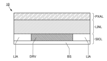
해상도가 높으며 화소에 대한 입력 신호의 지연이 억제된 표시 장치를 제공한다. 아래쪽으로부터 순차적으로 제 1 층, 제 2 층, 및 제 3 층이 형성된 표시 장치이다. 제 1 층은 구동 회로와 복수의 제 1 배선을 가지고, 제 2 층은 복수의 제 1 콘택트부를 가지고, 제 3 층은 화소 어레이와 복수의 제 2 배선을 가진다. 화소 어레이는 복수의 화소 회로를 가진다. 복수의 제 2 배선은 각각 평행하고, 또한 화소 어레이의 열 방향으로 연장되어 있는 배선이고, 복수의 화소 회로는 각각 복수의 제 2 배선에 전기적으로 접속되어 있다. 구동 회로는 제 1 방향을 따라 배열된 복수의 출력 단자를 가진다. 복수의 제 1 배선은 제 1 방향을 따라 수직으로 연장되어 있는 배선이고, 복수의 출력 단자는 각각 복수의 제 1 배선에 전기적으로 접속되어 있다. 복수의 제 1 배선은 각각 복수의 제 1 콘택트부를 통하여 복수의 제 2 배선에 전기적으로 접속되어 있다.A display device with high resolution and suppressed delay of input signals to pixels is provided. It is a display device in which a first layer, a second layer, and a third layer are formed sequentially from the bottom. The first layer has a driving circuit and a plurality of first wirings, the second layer has a plurality of first contact portions, and the third layer has a pixel array and a plurality of second wirings. The pixel array has a plurality of pixel circuits. The plurality of second wirings are parallel and extend in the column direction of the pixel array, and the plurality of pixel circuits are each electrically connected to the plurality of second wirings. The driving circuit has a plurality of output terminals arranged along a first direction. The plurality of first wires are wires extending vertically along the first direction, and the plurality of output terminals are each electrically connected to the plurality of first wires. Each of the plurality of first wirings is electrically connected to the plurality of second wirings through a plurality of first contact portions.

Description
본 발명의 일 형태는 표시 장치 및 전자 기기에 관한 것이다.One aspect of the present invention relates to display devices and electronic devices.
또한 본 발명의 일 형태는 상기 기술분야에 한정되지 않는다. 본 명세서 등에서 개시(開示)하는 발명의 기술분야는 물건, 구동 방법, 또는 제조 방법에 관한 것이다. 또는 본 발명의 일 형태는 공정(process), 기계(machine), 제품(manufacture), 또는 조성물(composition of matter)에 관한 것이다. 그러므로 더 구체적으로 본 명세서에서 개시하는 본 발명의 일 형태의 기술분야로서는 반도체 장치, 표시 장치, 액정 표시 장치, 발광 장치, 축전 장치, 촬상 장치, 기억 장치, 신호 처리 장치, 프로세서, 전자 기기, 시스템, 이들의 구동 방법, 이들의 제조 방법, 또는 이들의 검사 방법을 일례로서 들 수 있다.Additionally, one form of the present invention is not limited to the above technical field. The technical field of the invention disclosed in this specification and the like relates to products, driving methods, or manufacturing methods. Alternatively, one form of the present invention relates to a process, machine, manufacture, or composition of matter. Therefore, more specifically, the technical fields of one form of the present invention disclosed in this specification include semiconductor devices, display devices, liquid crystal display devices, light emitting devices, power storage devices, imaging devices, memory devices, signal processing devices, processors, electronic devices, and systems. , these driving methods, these manufacturing methods, or these inspection methods can be cited as examples.
VR(가상 현실), AR(증강 현실) 등의 XR 용도로 적용할 수 있는 표시 장치가 요구되고 있다. 이와 같은 표시 장치로서는, 예를 들어 높은 현실감 및 높은 몰입감을 사용자에게 주는 것이 요구되고 있다. 높은 현실감 및 높은 몰입감을 사용자에게 주는 방법으로서는, 예를 들어 표시 장치의 정세도를 높이는 것, 색 재현성을 높이는 것 등 표시 품질을 높이는 것이 있다.There is a demand for display devices that can be applied to XR applications such as VR (virtual reality) and AR (augmented reality). Such display devices are required to provide users with a high sense of reality and a high sense of immersion, for example. Methods for providing users with a high sense of reality and high immersion include improving display quality, such as increasing the resolution of the display device and improving color reproducibility.
또한 상기 표시 장치에 적용할 수 있는 장치의 예로서는, 액정 표시 장치, 유기 EL(Electro Luminescence), 발광 다이오드(LED: Light Emitting Diode) 등의 발광 디바이스를 포함한 발광 장치 등이 있다. 또한 특허문헌 1에는 유기 EL이 포함된 발광 디바이스를 포함하는, 고화소수 및 고정세(高精細)의 표시 장치가 개시되어 있다.Additionally, examples of devices that can be applied to the display device include light-emitting devices including light-emitting devices such as liquid crystal displays, organic EL (Electro Luminescence), and light-emitting diodes (LEDs). Additionally,
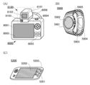
상술한 바와 같이, XR용 기기로서는 표시 품질이 높은 표시 장치가 요구되고 있다. 또한 XR용 표시 장치는 예를 들어 안경형 하우징, 고글형 하우징에 제공될 필요가 있기 때문에, 표시 장치의 크기를 작게 하는 것이 바람직하다. 구체적으로는, 예를 들어 VR용 기기의 경우, 표시 장치의 크기(대각선의 길이)는 1인치 이상 2인치 이하로 하는 것이 바람직하다. 또한 예를 들어 AR용 기기의 경우, 표시 장치의 크기는 3인치 이하로 하는 것이 바람직하고, 2인치 이하로 하는 것이 더 바람직하고, 1.5인치 이하로 하는 것이 더욱 바람직하다.As described above, display devices with high display quality are required as XR devices. Additionally, since the display device for XR needs to be provided in, for example, a glasses-type housing or a goggle-type housing, it is desirable to reduce the size of the display device. Specifically, for example, in the case of a VR device, it is desirable for the size (diagonal length) of the display device to be between 1 inch and 2 inches. Also, for example, in the case of an AR device, the size of the display device is preferably 3 inches or less, more preferably 2 inches or less, and even more preferably 1.5 inches or less.
한편 XR용 기기에 제공하는 표시 장치의 현실감 및 몰입감을 높이기 위해서는 해상도를 높일 필요가 있다. 이 경우, 예를 들어 정해진 크기 내에서, 화소 간, 배선 간 등의 피치 폭을 작게 하거나 화소의 크기를 작게 하는 등의 설계를 수행함으로써, 상기 크기 내에 제공되는 화소의 개수를 늘릴 수 있다. 다만 표시 장치 내의 화소의 개수가 증가되면 1프레임당 데이터양이 증가되기 때문에, 표시 장치를 구동시키는 구동 회로(소스 드라이버 회로, 게이트 드라이버 회로 등)의 고속화가 요구되고 있다.Meanwhile, in order to increase the realism and immersion of display devices provided for XR devices, it is necessary to increase the resolution. In this case, for example, within a given size, the number of pixels provided within the size can be increased by performing design such as reducing the pitch width between pixels or between wires or reducing the size of the pixels. However, as the number of pixels in a display device increases, the amount of data per frame increases, so speeding up the driving circuit (source driver circuit, gate driver circuit, etc.) that drives the display device is required.
또한 XR용 기기에 제공하는 표시 장치의 현실감 및 몰입감을 높이기 위해서는 구동 주파수를 높일 필요가 있다. 다만 구동 주파수가 높아질수록 1프레임당 입력 시간이 짧아지기 때문에, 1프레임 내에 표시 장치에 입력할 수 있는 데이터양이 작아지는 경우가 있다.Additionally, in order to increase the realism and immersion of display devices provided for XR devices, it is necessary to increase the driving frequency. However, as the driving frequency increases, the input time per frame becomes shorter, so the amount of data that can be input to the display device within one frame sometimes decreases.
본 발명의 일 형태는 회로 면적이 축소된 표시 장치를 제공하는 것을 과제 중 하나로 한다. 또는 본 발명의 일 형태는 소비 전력이 저감된 표시 장치를 제공하는 것을 과제 중 하나로 한다. 또는 본 발명의 일 형태는 표시 품질이 높은 표시 장치를 제공하는 것을 과제 중 하나로 한다. 또는 본 발명의 일 형태는 고정세하며 프레임 주파수가 높은 표시 장치를 제공하는 것을 과제 중 하나로 한다. 또는 본 발명의 일 형태는 신규 표시 장치를 제공하는 것을 과제 중 하나로 한다. 또는 본 발명의 일 형태는 상술한 표시 장치 중 어느 것을 가지는 전자 기기를 제공하는 것을 과제 중 하나로 한다.One aspect of the present invention aims to provide a display device with a reduced circuit area. Another object of one embodiment of the present invention is to provide a display device with reduced power consumption. Another object of one embodiment of the present invention is to provide a display device with high display quality. Another object of one embodiment of the present invention is to provide a display device with high definition and high frame frequency. Another object of one embodiment of the present invention is to provide a new display device. Another object of one embodiment of the present invention is to provide an electronic device having any of the above-described display devices.
또한 본 발명의 일 형태의 과제는 위에서 열거한 과제에 한정되지 않는다. 위에서 열거한 과제는 다른 과제의 존재를 방해하는 것이 아니다. 또한 다른 과제는 이하에 기재되고 본 항목에서는 언급되지 않은 과제이다. 본 항목에서 언급되지 않은 과제는 통상의 기술자라면 명세서 또는 도면 등의 기재에서 도출할 수 있는 것이고, 이들 기재에서 적절히 추출할 수 있다. 또한 본 발명의 일 형태는 위에서 열거한 과제 및 다른 과제 중 적어도 하나의 과제를 해결하는 것이다. 또한 본 발명의 일 형태는 위에서 열거한 과제 및 다른 과제 모두를 해결할 필요는 없다.Additionally, the problem of one embodiment of the present invention is not limited to the problems listed above. The tasks listed above do not prevent the existence of other tasks. Additionally, other tasks are listed below and are not mentioned in this section. Problems not mentioned in this item can be derived by a person skilled in the art from descriptions such as specifications or drawings, and can be appropriately extracted from these descriptions. Additionally, one form of the present invention solves at least one of the problems listed above and other problems. Additionally, one form of the present invention does not necessarily solve all of the problems listed above and other problems.
(1)(One)
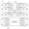
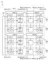
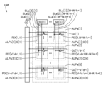
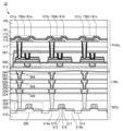
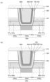
본 발명의 일 형태는 제 1 층과, 제 1 층의 위쪽에 위치하는 제 2 층과, 제 2 층의 위쪽에 위치하는 제 3 층을 가지는 표시 장치이다. 제 1 층은 구동 회로와 복수의 제 1 배선을 가지고, 제 2 층은 복수의 제 1 콘택트부를 가지고, 제 3 층은 화소 어레이와 복수의 제 2 배선을 가진다. 화소 어레이는 매트릭스상으로 배치된 복수의 화소 회로를 가지고, 구동 회로는 복수의 화소 회로를 제어하는 기능을 가진다. 복수의 제 2 배선은 각각 서로 평행하며 화소 어레이의 열 방향으로 연장되어 있는 배선이고, 복수의 화소 회로는 각각 복수의 제 2 배선에 전기적으로 접속되어 있다. 또한 구동 회로는 제 1 방향을 따라 배치되어 있는 복수의 출력 단자를 가진다. 복수의 제 1 배선은 제 1 방향에 대하여 수직으로 연장되어 있는 배선이고, 복수의 출력 단자는 각각 복수의 제 1 배선에 전기적으로 접속되어 있다. 복수의 제 1 배선은 각각 복수의 제 1 콘택트부를 통하여 복수의 제 2 배선에 전기적으로 접속되어 있다.One form of the present invention is a display device having a first layer, a second layer located above the first layer, and a third layer located above the second layer. The first layer has a driving circuit and a plurality of first wirings, the second layer has a plurality of first contact portions, and the third layer has a pixel array and a plurality of second wirings. The pixel array has a plurality of pixel circuits arranged in a matrix, and the driving circuit has a function of controlling the plurality of pixel circuits. The plurality of second wirings are parallel to each other and extend in the column direction of the pixel array, and the plurality of pixel circuits are each electrically connected to the plurality of second wirings. Additionally, the driving circuit has a plurality of output terminals arranged along the first direction. The plurality of first wirings are wirings extending perpendicularly to the first direction, and the plurality of output terminals are each electrically connected to the plurality of first wirings. Each of the plurality of first wirings is electrically connected to the plurality of second wirings through a plurality of first contact portions.
(2)(2)
또는 본 발명의 일 형태는, 상기 (1)에서 상면에서 보았을 때 복수의 제 1 콘택트부 중 하나가 화소 어레이의 내측이며 화소 회로의 내부, 또는 화소 회로의 외부에 위치하는 구성으로 하여도 좋다.Alternatively, one embodiment of the present invention may be configured so that when viewed from the top in (1) above, one of the plurality of first contact portions is inside the pixel array and is located inside the pixel circuit or outside the pixel circuit.
(3)(3)
또는 본 발명의 일 형태는 상기 (1) 또는 상기 (2)에서 제 1 층은 실리콘을 재료로 하는 반도체 기판과, 복수의 제 2 콘택트부를 가지는 구성으로 하여도 좋다. 특히 구동 회로는 채널 형성 영역에 실리콘을 가지는 복수의 트랜지스터를 가지는 것이 바람직하다. 또한 반도체 기판의 상면에는 복수의 제 1 배선이 되는 복수의 저저항 영역이 위치하고, 복수의 제 1 콘택트부와 복수의 저저항 영역 사이 각각에는 복수의 제 2 콘택트부가 위치하고, 복수의 저저항 영역은 복수의 트랜지스터 각각의 소스 및 드레인 중 한쪽을 가지는 것이 바람직하다.Alternatively, one embodiment of the present invention may have a configuration in (1) or (2) above, wherein the first layer has a semiconductor substrate made of silicon and a plurality of second contact portions. In particular, it is desirable for the driving circuit to have a plurality of transistors having silicon in the channel formation region. In addition, a plurality of low-resistance regions serving as a plurality of first wirings are located on the upper surface of the semiconductor substrate, and a plurality of second contact portions are positioned between the plurality of first contact portions and the plurality of low-resistance regions, and the plurality of low-resistance regions are It is desirable to have one of a source and a drain for each of the plurality of transistors.
(4)(4)
또는 본 발명의 일 형태는 제 1 층과, 제 1 층의 위쪽에 위치하는 제 3 층을 가지는 표시 장치이다. 제 1 층은 구동 회로 영역을 가지고, 제 3 층은 화소 어레이를 가진다. 화소 어레이는 복수의 화소 영역을 가지고, 구동 회로 영역은 복수의 로컬 드라이버 회로를 가진다. 복수의 로컬 드라이버 회로 중 하나는 복수의 화소 영역 중 어느 하나에 대응한다. 로컬 드라이버 회로는 대응하는 화소 영역에 포함되는 복수의 화소를 구동시키는 기능을 가진다. 또한 상면에서 보았을 때, 구동 회로 영역은 화소 어레이의 내측에 위치하고, 또한 복수의 화소 영역의 일부는 구동 회로 영역과 중첩되지 않는다.Alternatively, one embodiment of the present invention is a display device having a first layer and a third layer located above the first layer. The first layer has a driving circuit area, and the third layer has a pixel array. The pixel array has a plurality of pixel areas, and the driving circuit area has a plurality of local driver circuits. One of the plurality of local driver circuits corresponds to one of the plurality of pixel areas. The local driver circuit has the function of driving a plurality of pixels included in the corresponding pixel area. Additionally, when viewed from the top, the driving circuit area is located inside the pixel array, and some of the plurality of pixel areas do not overlap with the driving circuit area.
(5)(5)
또는 본 발명의 일 형태는 상기 (4)에서 복수의 화소 영역이 각각 복수의 배선을 가지는 구성으로 하여도 좋다. 또한 복수의 화소 영역에서 복수의 화소는 매트릭스상으로 위치하고, 복수의 배선은 매트릭스의 행마다 위치하고, 복수의 배선 중 하나는 같은 행에 위치하는 화소에 전기적으로 접속되어 있는 것이 바람직하다. 또한 복수의 배선은 각각 콘택트부를 가지고, 콘택트부는 화소의 내측 또는 인접한 화소 사이에 위치하는 것이 바람직하다.Alternatively, one embodiment of the present invention may be configured so that each of the plurality of pixel areas has a plurality of wiring lines in (4) above. Additionally, in a plurality of pixel areas, it is preferable that a plurality of pixels are located in a matrix, a plurality of wirings are located in each row of the matrix, and one of the plurality of wirings is electrically connected to a pixel located in the same row. Additionally, it is preferable that each of the plurality of wires has a contact portion, and the contact portion is located inside a pixel or between adjacent pixels.
(6)(6)
또는 본 발명의 일 형태는 상기 (4) 또는 상기 (5)에서 구동 회로 영역이 컨트롤러와 전압 생성 회로를 가지는 구성으로 하여도 좋다. 또한 컨트롤러는 외부로부터 입력되는 화상 신호와, 화상 신호의 송신처를 포함하는 어드레스 신호를 취득하는 기능과, 어드레스 신호에 따라 복수의 로컬 드라이버 회로를 선택하고 선택된 로컬 드라이버 회로에 화상 신호를 송신하는 기능을 가지는 것이 바람직하다. 또한 전압 생성 회로는 복수의 로컬 드라이버 회로 또는 화소에 대하여 공급하는 전압을 생성하는 기능을 가지는 것이 바람직하다.Alternatively, one embodiment of the present invention may be configured as in (4) or (5) above, where the driving circuit area includes a controller and a voltage generating circuit. In addition, the controller has a function of acquiring an externally input image signal and an address signal including the transmission destination of the image signal, and a function of selecting a plurality of local driver circuits according to the address signal and transmitting the image signal to the selected local driver circuit. It is desirable to have it. Additionally, the voltage generation circuit preferably has a function of generating voltage to be supplied to a plurality of local driver circuits or pixels.
(7)(7)
또는 본 발명의 일 형태는 상기 (4) 내지 (6) 중 어느 하나에서, 복수의 화소 영역 각각에 포함되는 화소가 유기 EL이 사용된 발광 디바이스와, 제 1 트랜지스터를 가지고, 복수의 로컬 드라이버 회로가 제 2 트랜지스터를 가지는 구성으로 하여도 좋다. 특히 제 1 트랜지스터는 채널 형성 영역에 금속 산화물을 가지는 것이 바람직하고, 제 2 트랜지스터는 채널 형성 영역에 실리콘을 가지는 것이 바람직하다.Alternatively, in one embodiment of the present invention, in any one of (4) to (6) above, a pixel included in each of the plurality of pixel areas has a light emitting device using organic EL, a first transistor, and a plurality of local driver circuits. It may be configured to include a second transistor. In particular, the first transistor preferably has metal oxide in the channel formation region, and the second transistor preferably has silicon in the channel formation region.
(8)(8)
또는 본 발명의 일 형태는 화소 어레이와, 구동 회로와, 제 1 배선과, 제 2 배선을 가지는 표시 장치이다. 화소 어레이는 각각 동일한 열을 포함하는 제 1 영역과 제 2 영역을 가지고, 제 1 영역은 제 1 화소 회로를 가지고, 제 2 영역은 제 2 화소 회로를 가진다. 또한 제 1 화소 회로와 제 2 화소 회로는 각각 화소 어레이에서 서로 동일한 열에 위치한다. 또한 제 1 배선은 제 1 영역의 내부에서 화소 어레이의 열 방향을 따라 연장되어 있는 배선이고, 제 2 배선은 제 2 영역의 내부에서 화소 어레이의 열 방향을 따라 연장되어 있는 배선이다. 구동 회로는 디멀티플렉서를 가지고, 제 1 화소 회로는 제 1 배선을 통하여 디멀티플렉서의 제 1 출력 단자에 전기적으로 접속되고, 제 2 화소 회로는 제 2 배선을 통하여 디멀티플렉서의 제 2 출력 단자에 전기적으로 접속되어 있다.Alternatively, one form of the present invention is a display device having a pixel array, a driving circuit, a first wiring, and a second wiring. The pixel array has a first area and a second area each including the same column, the first area has a first pixel circuit, and the second area has a second pixel circuit. Additionally, the first pixel circuit and the second pixel circuit are located in the same column in the pixel array. Additionally, the first wiring is a wiring extending along the column direction of the pixel array inside the first area, and the second wiring is a wiring extending along the column direction of the pixel array inside the second area. The driving circuit has a demultiplexer, the first pixel circuit is electrically connected to a first output terminal of the demultiplexer through a first wire, and the second pixel circuit is electrically connected to a second output terminal of the demultiplexer through a second wire. there is.
(9)(9)
또는 본 발명의 일 형태는 상기 (8)의 구성과 다른 화소 어레이와, 구동 회로와, 제 1 배선과, 제 2 배선을 가지는 표시 장치이다. 화소 어레이는 각각 동일한 열을 포함하는 제 1 영역과 제 2 영역을 가지고, 제 1 영역은 제 1 화소 회로를 가지고, 제 2 영역은 제 2 화소 회로를 가진다. 또한 제 1 화소 회로와 제 2 화소 회로는 각각 화소 어레이에서 서로 동일한 열에 위치한다. 또한 제 1 배선은 제 1 영역의 내부를 통과하여 화소 어레이의 열 방향을 따라 연장되어 있는 배선이고, 제 2 배선은 제 1 영역 및 제 2 영역 각각의 내부를 통과하여 화소 어레이의 열 방향을 따라 연장되어 있는 배선이다. 또한 구동 회로는 디멀티플렉서를 가진다. 제 1 화소 회로는 제 1 배선에 전기적으로 접속되고, 디멀티플렉서의 제 1 출력 단자는 제 1 배선에 전기적으로 접속되어 있다. 또한 제 2 화소 회로는 제 2 배선에 전기적으로 접속되고, 디멀티플렉서의 제 2 출력 단자는 제 2 배선에 전기적으로 접속되어 있다.Alternatively, one form of the present invention is a display device having a pixel array, a driving circuit, a first wiring, and a second wiring different from the configuration in (8) above. The pixel array has a first area and a second area each including the same column, the first area has a first pixel circuit, and the second area has a second pixel circuit. Additionally, the first pixel circuit and the second pixel circuit are located in the same column in the pixel array. In addition, the first wire passes through the inside of the first area and extends along the column direction of the pixel array, and the second wire passes through the inside of each of the first and second areas and extends along the column direction of the pixel array. It is an extended wiring. The driving circuit also has a demultiplexer. The first pixel circuit is electrically connected to the first wiring, and the first output terminal of the demultiplexer is electrically connected to the first wiring. Additionally, the second pixel circuit is electrically connected to the second wiring, and the second output terminal of the demultiplexer is electrically connected to the second wiring.
(10)(10)
또는 본 발명의 일 형태는 상기 (8) 및 상기 (9)의 구성과 다른 화소 어레이와, 구동 회로와, 제 1 배선과, 제 2 배선을 가지는 표시 장치이다. 화소 어레이는 각각 다른 열을 포함하는 제 1 영역과, 제 2 영역을 가지고, 제 1 영역은 제 1 화소 회로를 가지고, 제 2 영역은 제 2 화소 회로를 가진다. 또한 제 1 화소 회로와 제 2 화소 회로는 각각 화소 어레이에서 서로 다른 열에 위치하고, 제 1 배선은 제 1 영역의 내부에서 화소 어레이의 열 방향을 따라 연장되어 있는 배선이고, 제 2 배선은 제 2 영역의 내부에서 화소 어레이의 열 방향을 따라 연장되어 있는 배선이다. 구동 회로는 디멀티플렉서를 가지고, 제 1 화소 회로는 제 1 배선을 통하여 디멀티플렉서의 제 1 출력 단자에 전기적으로 접속되고, 제 2 화소 회로는 제 2 배선을 통하여 디멀티플렉서의 제 2 출력 단자에 전기적으로 접속되어 있다.Alternatively, one form of the present invention is a display device having a pixel array, a driving circuit, a first wiring, and a second wiring different from the configurations of (8) and (9) above. The pixel array has a first area and a second area each including different columns, the first area has a first pixel circuit, and the second area has a second pixel circuit. Additionally, the first pixel circuit and the second pixel circuit are each located in different columns in the pixel array, the first wiring is a wiring extending along the column direction of the pixel array inside the first region, and the second wiring is a wiring extending in the second region. It is a wiring that extends along the column direction of the pixel array inside the . The driving circuit has a demultiplexer, the first pixel circuit is electrically connected to a first output terminal of the demultiplexer through a first wire, and the second pixel circuit is electrically connected to a second output terminal of the demultiplexer through a second wire. there is.
(11)(11)
또는 본 발명의 일 형태는 상기 (8) 내지 (10) 중 어느 하나에서 제 3 배선과 제 4 배선을 가지는 구성으로 하여도 좋다. 또한 제 1 화소 회로는 제 1 트랜지스터를 가지고, 제 2 화소 회로는 제 2 트랜지스터를 가지는 구성으로 하여도 좋다. 제 3 배선은 제 1 영역의 내부에서, 화소 어레이의 행 방향을 따라 연장된 배선이고, 제 4 배선은 제 2 영역의 내부에서 화소 어레이의 행 방향을 따라 연장된 배선인 것이 바람직하다. 또한 제 1 트랜지스터의 소스 및 드레인 중 한쪽은 제 1 배선에 전기적으로 접속되고, 제 1 트랜지스터의 게이트는 제 3 배선에 전기적으로 접속되어 있는 것이 바람직하다. 또한 제 2 트랜지스터의 소스 및 드레인 중 한쪽은 제 2 배선에 전기적으로 접속되고, 제 2 트랜지스터의 게이트는 제 4 배선에 전기적으로 접속되어 있는 것이 바람직하다.Alternatively, one embodiment of the present invention may be configured to have a third wiring and a fourth wiring in any one of (8) to (10) above. Additionally, the first pixel circuit may have a first transistor, and the second pixel circuit may have a second transistor. Preferably, the third wiring is a wiring extending along the row direction of the pixel array inside the first area, and the fourth wiring is a wiring extending along the row direction of the pixel array inside the second area. Additionally, it is preferable that one of the source and drain of the first transistor is electrically connected to the first wiring, and the gate of the first transistor is electrically connected to the third wiring. Additionally, it is preferable that one of the source and drain of the second transistor is electrically connected to the second wiring, and the gate of the second transistor is electrically connected to the fourth wiring.
(12)(12)
또는 본 발명의 일 형태는 상기 (11)에서 제 5 배선과, 제 6 배선과, 제 7 배선과, 제 8 배선을 가지는 구성으로 하여도 좋다. 또한 제 1 영역은 제 3 화소 회로를 가지고, 제 2 영역은 제 4 화소 회로를 가지는 구성으로 하여도 좋다. 또한 제 3 화소 회로는 제 3 트랜지스터를 가지고, 제 4 화소 회로는 제 4 트랜지스터를 가지는 구성으로 하여도 좋다. 제 3 화소 회로는 화소 어레이에서, 제 1 화소 회로와 다른 열에 위치하고, 제 4 화소 회로는 화소 어레이에서 제 2 화소 회로와 다른 열에 위치하는 것이 바람직하다. 또한 제 5 배선은 제 1 영역의 내부에서 화소 어레이의 열 방향을 따라 연장된 배선이고, 제 6 배선은 제 2 영역의 내부에서 화소 어레이의 열 방향을 따라 연장된 배선이고, 제 7 배선은 제 1 영역의 내부에서 화소 어레이의 행 방향을 따라 연장된 배선이고, 제 8 배선은 제 2 영역의 내부에서 화소 어레이의 행 방향을 따라 연장된 배선인 것이 바람직하다. 또한 제 3 트랜지스터의 소스 및 드레인 중 한쪽은 제 5 배선에 전기적으로 접속되고, 제 3 트랜지스터의 게이트는 제 7 배선에 전기적으로 접속되어 있는 것이 바람직하다. 또한 제 4 트랜지스터의 소스 및 드레인 중 한쪽은 제 6 배선에 전기적으로 접속되고, 제 4 트랜지스터의 게이트는 제 8 배선에 전기적으로 접속되어 있는 것이 바람직하다. 또한 제 5 배선은 디멀티플렉서의 제 3 출력 단자에 전기적으로 접속되고, 제 6 배선은 디멀티플렉서의 제 4 출력 단자에 전기적으로 접속되어 있는 것이 바람직하다.Alternatively, one embodiment of the present invention may be configured to have a fifth wiring, a sixth wiring, a seventh wiring, and an eighth wiring in (11) above. Additionally, the first area may have a third pixel circuit, and the second area may have a fourth pixel circuit. Additionally, the third pixel circuit may have a third transistor, and the fourth pixel circuit may have a fourth transistor. Preferably, the third pixel circuit is located in a different column from the first pixel circuit in the pixel array, and the fourth pixel circuit is located in a different column than the second pixel circuit in the pixel array. Additionally, the fifth wire is a wire extending along the column direction of the pixel array inside the first area, the sixth wire is a wire extending along the column direction of the pixel array inside the second area, and the seventh wire is a wire extending along the column direction of the pixel array inside the second area. It is preferable that the wiring extends along the row direction of the pixel array inside the first region, and the eighth wiring is preferably extended along the row direction of the pixel array inside the second region. Additionally, it is preferable that one of the source and drain of the third transistor is electrically connected to the fifth wiring, and the gate of the third transistor is electrically connected to the seventh wiring. Additionally, it is preferable that one of the source and drain of the fourth transistor is electrically connected to the sixth wiring, and the gate of the fourth transistor is electrically connected to the eighth wiring. Additionally, it is preferable that the fifth wire is electrically connected to the third output terminal of the demultiplexer, and the sixth wire is electrically connected to the fourth output terminal of the demultiplexer.
(13)(13)
또는 본 발명의 일 형태는 상기 (8) 내지 (12) 중 어느 하나에서 제 1 층과, 상기 제 1 층의 위쪽에 위치하는 제 3 층을 가지는 구성으로 하여도 좋다. 특히 제 1 층은 구동 회로를 가지고, 제 3 층은 상기 화소 어레이를 가지는 구성으로 하는 것이 바람직하다.Alternatively, one embodiment of the present invention may be configured to have a first layer and a third layer located above the first layer in any one of (8) to (12) above. In particular, it is preferable that the first layer has a driving circuit and the third layer has the pixel array.
(14)(14)
또는 본 발명의 일 형태는 상기 (1) 내지 (13) 중 어느 하나의 표시 장치와 하우징을 가지는 전자 기기이다.Alternatively, one embodiment of the present invention is an electronic device having the display device and housing according to any one of (1) to (13) above.
또한 본 명세서 등에서 반도체 장치란, 반도체 특성을 이용한 장치이고, 반도체 소자(트랜지스터, 다이오드, 포토다이오드 등)를 포함한 회로, 이 회로를 포함한 장치 등을 말한다. 또한 반도체 특성을 이용함으로써 기능할 수 있는 장치 전반을 말한다. 예를 들어 집적 회로, 집적 회로를 포함한 칩, 및 패키지에 칩을 수납한 전자 부품은 반도체 장치의 일례이다. 또한 기억 장치, 표시 장치, 발광 장치, 조명 장치, 및 전자 기기 등은 그 자체가 반도체 장치인 경우가 있고, 반도체 장치를 가지는 경우가 있다.Additionally, in this specification and the like, a semiconductor device refers to a device that utilizes semiconductor characteristics, and refers to a circuit including a semiconductor element (transistor, diode, photodiode, etc.), a device including this circuit, etc. It also refers to the overall device that can function by utilizing semiconductor characteristics. For example, integrated circuits, chips containing integrated circuits, and electronic components containing the chips in packages are examples of semiconductor devices. Additionally, memory devices, display devices, light-emitting devices, lighting devices, and electronic devices may themselves be semiconductor devices or may have semiconductor devices.
또한 본 명세서 등에서 X와 Y가 접속된다고 기재되는 경우에는, X와 Y가 전기적으로 접속되는 경우와, X와 Y가 기능적으로 접속되는 경우와, X와 Y가 직접 접속되는 경우가 본 명세서 등에 개시되어 있는 것으로 한다. 따라서 소정의 접속 관계, 예를 들어 도면 또는 문장에 나타낸 접속 관계에 한정되지 않고, 도면 또는 문장에 나타낸 접속 관계 이외의 것도 도면 또는 문장에 개시되어 있는 것으로 한다. X, Y는 대상물(예를 들어 장치, 소자, 회로, 배선, 전극, 단자, 도전막, 층 등)인 것으로 한다.In addition, when X and Y are described as connected in this specification, etc., the case where X and Y are electrically connected, the case where X and Y are functionally connected, and the case where X and Y are directly connected are disclosed in this specification, etc. It is assumed that it is done. Therefore, it is not limited to a predetermined connection relationship, for example, the connection relationship shown in the drawing or text, and connection relationships other than those shown in the drawing or text are also disclosed in the drawing or text. X and Y are assumed to be objects (e.g., devices, elements, circuits, wiring, electrodes, terminals, conductive films, layers, etc.).
X와 Y가 전기적으로 접속되는 경우에는, 일례로서 X와 Y를 전기적으로 접속할 수 있는 소자(예를 들어 스위치, 트랜지스터, 용량 소자, 인덕터, 저항 소자, 다이오드, 표시 디바이스, 발광 디바이스, 부하 등)가 X와 Y 사이에 하나 이상 접속될 수 있다. 또한 스위치는 온과 오프가 제어되는 기능을 가진다. 즉 스위치는 도통 상태(온 상태) 또는 비도통 상태(오프 상태)가 되어, 전류를 흘릴지 여부를 제어하는 기능을 가진다.When X and Y are electrically connected, as an example, an element that can electrically connect One or more can be connected between X and Y. Additionally, the switch has the function of being controlled on and off. In other words, the switch has the function of controlling whether or not to flow current by being in a conductive state (on state) or non-conductive state (off state).
X와 Y가 기능적으로 접속되는 경우에는, 일례로서 X와 Y를 기능적으로 접속할 수 있는 회로(예를 들어 논리 회로(인버터, NAND 회로, NOR 회로 등), 신호 변환 회로(디지털 아날로그 변환 회로, 아날로그 디지털 변환 회로, 감마 보정 회로 등), 전위 레벨 변환 회로(전원 회로(승압 회로, 강압 회로 등), 신호의 전위 레벨을 바꾸는 레벨 시프터 회로 등), 전압원, 전류원, 전환 회로, 증폭 회로(신호 진폭 또는 전류량 등을 크게 할 수 있는 회로, 연산 증폭기, 차동 증폭 회로, 소스 폴로어 회로, 버퍼 회로 등), 신호 생성 회로, 기억 회로, 제어 회로 등)가 X와 Y 사이에 하나 이상 접속될 수 있다. 또한 일례로서, X와 Y 사이에 다른 회로를 끼워도 X로부터 출력된 신호가 Y로 전달되는 경우에는, X와 Y는 기능적으로 접속되는 것으로 한다.When X and Y are functionally connected, as an example, a circuit that can functionally connect digital conversion circuit, gamma correction circuit, etc.), potential level conversion circuit (power circuit (boosting circuit, step-down circuit, etc.), level shifter circuit that changes the potential level of the signal, etc.), voltage source, current source, switching circuit, amplification circuit (signal amplitude) Alternatively, one or more circuits (operational amplifiers, differential amplifier circuits, source follower circuits, buffer circuits, etc.) that can increase the amount of current, signal generation circuits, memory circuits, control circuits, etc.) may be connected between X and Y. . Also, as an example, if a signal output from X is transmitted to Y even if another circuit is inserted between X and Y, X and Y are considered to be functionally connected.
또한 X와 Y가 전기적으로 접속된다고 명시적으로 기재되는 경우에는, X와 Y가 전기적으로 접속되는 경우(즉 X와 Y가 사이에 다른 소자 또는 다른 회로를 끼워 접속되는 경우)와, X와 Y가 직접 접속되는 경우(즉 X와 Y가 사이에 다른 소자 또는 다른 회로를 끼우지 않고 접속되는 경우)를 포함하는 것으로 한다.Additionally, when it is explicitly stated that X and Y are electrically connected, there is a case where This shall include the case where is directly connected (i.e., when X and Y are connected without interposing other elements or other circuits between them).
또한 예를 들어 "X와, Y와, 트랜지스터의 소스(또는 제 1 단자 등)와, 드레인(또는 제 2 단자 등)은 서로 전기적으로 접속되고, X, 트랜지스터의 소스(또는 제 1 단자 등), 트랜지스터의 드레인(또는 제 2 단자 등), Y의 순서로 전기적으로 접속된다"라고 표현할 수 있다. 또는 "트랜지스터의 소스(또는 제 1 단자 등)는 X에 전기적으로 접속되고, 트랜지스터의 드레인(또는 제 2 단자 등)은 Y에 전기적으로 접속되고, X, 트랜지스터의 소스(또는 제 1 단자 등), 트랜지스터의 드레인(또는 제 2 단자 등), Y는 이 순서대로 전기적으로 접속된다"라고 표현할 수 있다. 또는 "X는 트랜지스터의 소스(또는 제 1 단자 등)와 드레인(또는 제 2 단자 등)을 통하여 Y에 전기적으로 접속되고, X, 트랜지스터의 소스(또는 제 1 단자 등), 트랜지스터의 드레인(또는 제 2 단자 등), Y는 이 접속 순서로 제공된다"라고 표현할 수 있다. 이들 예와 같은 표현 방법을 사용하여 회로 구성에서의 접속 순서에 대하여 규정함으로써, 트랜지스터의 소스(또는 제 1 단자 등)와 드레인(또는 제 2 단자 등)을 구별하여 기술적 범위를 결정할 수 있다. 또한 이들 표현 방법은 일례이고, 이들 표현 방법에 한정되지 않는다. 여기서 X, Y는 대상물(예를 들어 장치, 소자, 회로, 배선, 전극, 단자, 도전막, 층 등)인 것으로 한다.Also, for example, "X, Y, the source (or first terminal, etc.) of the transistor, and the drain (or second terminal, etc.) are electrically connected to each other, and , the drain (or second terminal, etc.) of the transistor, and Y are electrically connected in that order.” or "the source (or first terminal, etc.) of the transistor is electrically connected to X, the drain (or second terminal, etc.) of the transistor is electrically connected to Y, and , the drain (or second terminal, etc.) of the transistor, Y are electrically connected in this order.” or "X is electrically connected to Y through the source (or first terminal, etc.) and drain (or second terminal, etc.) of the transistor, and 2nd terminal, etc.), Y is provided in this connection order.” By specifying the connection order in the circuit configuration using expression methods such as these examples, the technical scope can be determined by distinguishing between the source (or first terminal, etc.) and drain (or second terminal, etc.) of the transistor. Additionally, these expression methods are examples and are not limited to these expression methods. Here, X and Y are assumed to be objects (e.g., devices, elements, circuits, wiring, electrodes, terminals, conductive films, layers, etc.).
또한 회로도상 독립된 구성 요소들이 전기적으로 접속되는 것처럼 도시되어 있는 경우에도, 하나의 구성 요소가 복수의 구성 요소의 기능을 겸비하는 경우도 있다. 예를 들어 배선의 일부가 전극으로서도 기능하는 경우에는, 하나의 도전막이 배선의 기능 및 전극의 기능의 양쪽의 구성 요소의 기능을 겸비한다. 따라서 본 명세서에서의 전기적인 접속이란, 이와 같이 하나의 도전막이 복수의 구성 요소의 기능을 겸비하는 경우도 그 범주에 포함한다.Additionally, even when independent components are shown as electrically connected in a circuit diagram, there are cases where one component has the functions of multiple components. For example, when a part of the wiring also functions as an electrode, one conductive film functions as a component of both the wiring function and the electrode function. Therefore, the term electrical connection in this specification also includes cases where one conductive film functions as a plurality of components.
또한 본 명세서 등에서 "저항 소자"란, 예를 들어 0Ω보다 저항값이 높은 회로 소자, 0Ω보다 저항값이 높은 배선 등으로 할 수 있다. 그러므로 본 명세서 등에서 "저항 소자"는 저항값을 가지는 배선, 소스와 드레인 간을 전류가 흐르는 트랜지스터, 다이오드, 코일 등을 포함하는 것으로 한다. 그러므로 "저항 소자"라는 용어는 "저항", "부하", "저항값을 가지는 영역" 등의 용어로 바꿔 말할 수 있는 경우가 있다. 반대로 "저항", "부하", "저항값을 가지는 영역"이라는 용어는 "저항 소자" 등의 용어로 바꿔 말할 수 있는 경우가 있다. 저항값은 예를 들어 바람직하게는 1mΩ 이상 10Ω 이하, 더 바람직하게는 5mΩ 이상 5Ω 이하, 더욱 바람직하게는 10mΩ 이상 1Ω 이하로 할 수 있다. 또한 예를 들어 1Ω 이상 1×10⁹Ω 이하로 하여도 좋다.In addition, in this specification and the like, the term "resistance element" can be, for example, a circuit element with a resistance value higher than 0Ω, wiring with a resistance value higher than 0Ω, etc. Therefore, in this specification and the like, “resistance elements” are intended to include wiring having a resistance value, transistors, diodes, coils, etc. through which current flows between the source and drain. Therefore, the term “resistance element” may be replaced by terms such as “resistance,” “load,” or “area with a resistance value.” Conversely, the terms “resistance,” “load,” and “area with a resistance value” may be replaced with terms such as “resistance element.” The resistance value can be, for example, preferably 1 mΩ or more and 10 Ω or less, more preferably 5 mΩ or more and 5 Ω or less, and even more preferably 10 mΩ or more and 1 Ω or less. Also, for example, it may be 1Ω or more and 1×10 9 Ω or less.
또한 본 명세서 등에서 "용량 소자"는, 예를 들어 정전 용량이 0F보다 높은 회로 소자, 정전 용량이 0F보다 높은 배선의 영역, 기생 용량, 트랜지스터의 게이트 용량 등으로 할 수 있다. 또한 "용량 소자", "기생 용량", "게이트 용량" 등이라는 용어는 "용량" 등의 용어로 바꿔 말할 수 있는 경우가 있다. 반대로 "용량"이라는 용어는 "용량 소자", "기생 용량", "게이트 용량" 등의 용어로 바꿔 말할 수 있는 경우가 있다. 또한 "용량"의 "한 쌍의 전극"이라는 용어는 "한 쌍의 도전체", "한 쌍의 도전 영역", "한 쌍의 영역" 등으로 바꿔 말할 수 있다. 또한 정전 용량은 예를 들어 0.05fF 이상 10pF 이하로 할 수 있다. 또한 예를 들어 1pF 이상 10μF 이하로 하여도 좋다.In addition, in this specification and the like, “capacitance element” may be, for example, a circuit element with a capacitance higher than 0F, a wiring area with a capacitance higher than 0F, a parasitic capacitance, a gate capacitance of a transistor, etc. Additionally, terms such as “capacitance element”, “parasitic capacitance”, “gate capacitance”, etc. may be replaced by terms such as “capacitance”. Conversely, the term "capacitance" may be interchanged with terms such as "capacitance element", "parasitic capacitance", and "gate capacitance". Additionally, the term “a pair of electrodes” in “capacitance” can be replaced with “a pair of conductors,” “a pair of conductive regions,” “a pair of regions,” etc. Additionally, the capacitance can be, for example, 0.05fF or more and 10pF or less. Also, for example, it may be set to 1pF or more and 10μF or less.
또한 본 명세서 등에서 트랜지스터는 게이트, 소스, 및 드레인이라고 불리는 3개의 단자를 포함한다. 게이트는 트랜지스터의 도통 상태를 제어하는 제어 단자이다. 소스 또는 드레인으로서 기능하는 2개의 단자는 트랜지스터의 입출력 단자이다. 2개의 입출력 단자는 트랜지스터의 도전형(n채널형, p채널형) 및 트랜지스터의 3개의 단자에 인가되는 전위의 높낮이에 따라, 한쪽이 소스가 되고 다른 쪽이 드레인이 된다. 그러므로 본 명세서 등에서는, 소스 및 드레인이라는 용어는 서로 바꿔 말할 수 있는 경우가 있다. 또한 본 명세서 등에서는, 트랜지스터의 접속 관계를 설명하는 경우, "소스 및 드레인 중 한쪽"(또는 제 1 전극 또는 제 1 단자), "소스 및 드레인 중 다른 쪽"(또는 제 2 전극 또는 제 2 단자)이라는 표기를 사용한다. 또한 트랜지스터의 구조에 따라서는 상술한 3개의 단자에 더하여 백 게이트를 포함하는 경우가 있다. 이 경우, 본 명세서 등에서 트랜지스터의 게이트 및 백 게이트 중 한쪽을 제 1 게이트라고 부르고, 트랜지스터의 게이트 및 백 게이트 중 다른 쪽을 제 2 게이트라고 부르는 경우가 있다. 또한 같은 트랜지스터에서 "게이트"와 "백 게이트"라는 용어는 서로 바꿀 수 있는 경우가 있다. 또한 트랜지스터가 3개 이상의 게이트를 포함하는 경우, 본 명세서 등에서는 각 게이트를 제 1 게이트, 제 2 게이트, 제 3 게이트 등이라고 부를 수 있다.Additionally, in this specification and the like, the transistor includes three terminals called a gate, source, and drain. The gate is a control terminal that controls the conduction state of the transistor. The two terminals that function as source or drain are the input and output terminals of the transistor. One of the two input/output terminals becomes the source and the other becomes the drain, depending on the conductivity type of the transistor (n-channel type, p-channel type) and the height of the potential applied to the three terminals of the transistor. Therefore, in this specification and the like, the terms source and drain may be interchanged with each other. Additionally, in this specification and the like, when explaining the connection relationship of a transistor, “one of the source and the drain” (or the first electrode or the first terminal), “the other of the source and the drain” (or the second electrode or the second terminal) ) is used. Additionally, depending on the structure of the transistor, a back gate may be included in addition to the three terminals described above. In this case, in this specification and the like, one of the gate and back gate of the transistor may be called a first gate, and the other of the gate and back gate of the transistor may be called a second gate. Additionally, the terms "gate" and "back gate" are sometimes interchangeable for the same transistor. Additionally, when the transistor includes three or more gates, each gate may be referred to as a first gate, second gate, third gate, etc. in this specification and the like.
예를 들어 본 명세서 등에서 트랜지스터의 일례로서는, 2개 이상의 게이트 전극을 포함한 멀티 게이트 구조의 트랜지스터를 사용할 수 있다. 멀티 게이트 구조로 하면, 채널 형성 영역이 직렬로 접속되기 때문에, 복수의 트랜지스터가 직렬로 접속된다. 따라서 멀티 게이트 구조로 하면, 오프 전류의 감소, 트랜지스터의 내압 향상(신뢰성 향상)을 도모할 수 있다. 또는 멀티 게이트 구조로 하면, 포화 영역에서 동작할 때, 드레인과 소스 사이의 전압이 변화되어도 드레인과 소스 사이의 전류가 그다지 변화되지 않기 때문에, 기울기가 평평한 전압·전류 특성을 얻을 수 있다. 기울기가 평평한 전압·전류 특성을 이용하면, 이상적인 전류원 회로 또는 저항값이 매우 높은 능동 부하를 실현할 수 있다. 그 결과, 특성이 좋은 차동 회로 또는 커런트 미러 회로 등을 실현할 수 있다.For example, as an example of a transistor in this specification and the like, a transistor with a multi-gate structure including two or more gate electrodes can be used. In the case of a multi-gate structure, since the channel formation regions are connected in series, a plurality of transistors are connected in series. Therefore, by using a multi-gate structure, the off-state current can be reduced and the withstand voltage of the transistor can be improved (reliability improved). Alternatively, with a multi-gate structure, when operating in the saturation region, the current between the drain and source does not change much even if the voltage between the drain and source changes, so voltage and current characteristics with a flat slope can be obtained. By using voltage and current characteristics with flat slopes, an ideal current source circuit or an active load with a very high resistance value can be realized. As a result, a differential circuit or current mirror circuit with good characteristics can be realized.
또한 회로도에서 단일의 회로 소자가 도시되어 있는 경우에도 상기 회로 소자가 복수의 회로 소자를 포함하는 경우가 있다. 예를 들어 회로도에서 하나의 저항 소자가 도시되어 있는 경우에는 2개 이상의 저항 소자가 직렬로 전기적으로 접속되어 있는 경우를 포함하는 것으로 한다. 또한 예를 들어 회로도에서 하나의 용량 소자가 도시되어 있는 경우에는 2개 이상의 용량 소자가 병렬로 전기적으로 접속되어 있는 경우를 포함하는 것으로 한다. 또한 예를 들어 회로도에서 하나의 트랜지스터가 도시되어 있는 경우에는 2개 이상의 트랜지스터가 직렬로 전기적으로 접속되고, 또한 각 트랜지스터의 게이트가 서로 전기적으로 접속되어 있는 경우를 포함하는 것으로 한다. 또한 이와 마찬가지로 예를 들어 회로도에서 하나의 스위치가 도시되어 있는 경우에는 상기 스위치가 2개 이상의 트랜지스터를 포함하고, 2개 이상의 트랜지스터가 직렬 또는 병렬로 전기적으로 접속되고, 각 트랜지스터의 게이트가 서로 전기적으로 접속되어 있는 경우를 포함하는 것으로 한다.Additionally, even when a single circuit element is shown in a circuit diagram, the circuit element may include a plurality of circuit elements. For example, when a single resistance element is shown in a circuit diagram, this includes cases where two or more resistance elements are electrically connected in series. Also, for example, when one capacitive element is shown in a circuit diagram, this includes the case where two or more capacitive elements are electrically connected in parallel. Also, for example, when one transistor is shown in a circuit diagram, this includes cases where two or more transistors are electrically connected in series and the gates of each transistor are electrically connected to each other. Likewise, for example, when one switch is shown in a circuit diagram, the switch includes two or more transistors, the two or more transistors are electrically connected in series or parallel, and the gates of each transistor are electrically connected to each other. This includes cases where it is connected.
또한 본 명세서 등에서, 회로 구성 및/또는 디바이스 구조에 따라, 노드를 단자, 배선, 전극, 도전층, 도전체, 불순물 영역 등으로 바꿔 말할 수 있다. 또한 단자, 배선 등을 노드로 바꿔 말할 수 있다.Additionally, in this specification and the like, a node may be referred to as a terminal, wiring, electrode, conductive layer, conductor, impurity region, etc., depending on the circuit configuration and/or device structure. Additionally, terminals, wiring, etc. can be referred to as nodes.
또한 본 명세서 등에서 "전압"과 "전위"는 적절히 바꿔 말할 수 있다. "전압"은 기준이 되는 전위와의 전위차를 말하고, 예를 들어 기준이 되는 전위를 그라운드 전위(접지 전위)로 하면, "전압"을 "전위"로 바꿔 말할 수 있다. 또한 그라운드 전위는 반드시 0V를 의미하는 것은 아니다. 또한 전위는 상대적인 것이고, 기준이 되는 전위가 변화됨으로써, 배선에 공급되는 전위, 회로 등에 인가되는 전위, 회로 등으로부터 출력되는 전위 등도 변화된다.Additionally, in this specification and elsewhere, “voltage” and “potential” can be appropriately interchanged. “Voltage” refers to the potential difference from the reference potential. For example, if the reference potential is the ground potential, “voltage” can be changed to “potential.” Also, ground potential does not necessarily mean 0V. Additionally, potential is relative, and as the reference potential changes, the potential supplied to the wiring, the potential applied to the circuit, etc., and the potential output from the circuit, etc. also change.
또한 본 명세서 등에서 "고레벨 전위", "저레벨 전위"라는 용어는 특정의 전위를 의미하는 것은 아니다. 예를 들어 2개의 배선의 양쪽이 "고레벨 전위를 공급하는 배선으로서 기능한다"라고 기재되는 경우, 양쪽의 배선이 공급하는 각 고레벨 전위는 서로 같지 않아도 된다. 또한 이와 마찬가지로 2개의 배선의 양쪽이 "저레벨 전위를 공급하는 배선으로서 기능한다"라고 기재되는 경우, 양쪽의 배선이 공급하는 각 저레벨 전위는 서로 같지 않아도 된다.Additionally, in this specification and the like, the terms “high level potential” and “low level potential” do not mean a specific potential. For example, if both sides of two wirings are described as "functioning as wiring that supplies high-level potential," the high-level potentials supplied by both wirings do not need to be the same. Likewise, when both sides of two wires are described as "functioning as wires that supply low-level potentials," the low-level potentials supplied by both wires do not need to be the same.
"전류"란 전하의 이동 현상(전기 전도)을 말하고, 예를 들어 "양의 하전체(荷電體)의 전기 전도가 발생하고 있다"라는 기재는, "그 반대 방향으로 음의 하전체의 전기 전도가 발생하고 있다"라고 바꿔 말할 수 있다. 그러므로 본 명세서 등에서 "전류"란 별도의 설명이 없는 한, 캐리어의 이동에 따른 전하의 이동 현상(전기 전도)을 말하는 것으로 한다. 여기서 캐리어란 전자, 정공, 음이온, 양이온, 착이온 등이고, 전류가 흐르는 시스템(예를 들어 반도체, 금속, 전해액, 진공 중 등)에 따라 캐리어가 다르다. 또한 배선 등에서의 "전류의 방향"은 양전하가 되는 캐리어가 이동하는 방향이고, 양의 전류량으로 기재한다. 바꿔 말하면, 음전하가 되는 캐리어가 이동하는 방향은 전류의 방향과 반대 방향이고, 음의 전류량으로 표현된다. 따라서 본 명세서 등에서 전류의 양과 음(또는 전류의 방향)에 대하여 별도의 설명이 없는 경우, "소자 A로부터 소자 B로 전류가 흐른다" 등의 기재는 "소자 B로부터 소자 A로 전류가 흐른다" 등으로 바꿔 말할 수 있는 것으로 한다. 또한 "소자 A에 전류가 입력된다" 등의 기재는 "소자 A로부터 전류가 출력된다" 등으로 바꿔 말할 수 있는 것으로 한다.“Current” refers to the phenomenon of electric charge movement (electrical conduction). For example, a statement that “electrical conduction of a positively charged body is occurring” means “electricity of a negatively charged body in the opposite direction.” It can be said differently, “Evangelism is occurring.” Therefore, in this specification, etc., unless otherwise specified, “current” refers to the phenomenon of charge movement (electrical conduction) due to the movement of carriers. Here, carriers include electrons, holes, negative ions, cations, and complex ions, and the carriers differ depending on the system through which the current flows (e.g., semiconductor, metal, electrolyte, vacuum, etc.). Additionally, the “direction of current” in wiring, etc. is the direction in which positive carriers move, and is described as the amount of positive current. In other words, the direction in which negatively charged carriers move is opposite to the direction of the current, and is expressed as the amount of negative current. Therefore, if there is no separate explanation regarding the positive and negative current (or direction of current) in this specification, etc., statements such as “current flows from element A to element B” are replaced with “current flows from element B to element A,” etc. Make it something that can be changed to . Additionally, statements such as “current is input to element A” can be rephrased as “current is output from element A”, etc.
또한 본 명세서 등에서 "제 1", "제 2", "제 3"이라는 서수사는 구성 요소의 혼동을 피하기 위하여 붙인 것이다. 따라서 구성 요소의 개수를 한정하는 것이 아니다. 또한 구성 요소의 순서를 한정하는 것이 아니다. 예를 들어 본 명세서 등의 실시형태 중 하나에서 "제 1"로 언급된 구성 요소가 다른 실시형태 또는 청구범위에서 "제 2"로 언급된 구성 요소가 될 수도 있다. 또한 예를 들어 본 명세서 등의 실시형태 중 하나에서 "제 1"로 언급된 구성 요소가 다른 실시형태 또는 청구범위에서 생략될 수도 있다.Additionally, in this specification, etc., the ordinal numerals “first,” “second,” and “third” are added to avoid confusion between constituent elements. Therefore, the number of components is not limited. Also, the order of components is not limited. For example, an element referred to as “first” in one of the embodiments of this specification or the like may be an element referred to as “second” in another embodiment or in the claims. Additionally, for example, an element referred to as “first” in one of the embodiments of this specification or the like may be omitted in other embodiments or claims.
또한 본 명세서 등에서 "위에", "아래에" 등의 배치를 나타내는 용어는 구성끼리의 위치 관계를 도면을 참조하여 설명하기 위하여 편의상 사용하고 있는 경우가 있다. 또한 구성끼리의 위치 관계는 각 구성을 묘사하는 방향에 따라 적절히 변화된다. 따라서 명세서 등에서 설명한 용어에 한정되지 않고, 상황에 따라 적절히 바꿔 말할 수 있다. 예를 들어 "도전체의 상면에 위치하는 절연체"라는 표현은, 나타낸 도면의 방향을 180° 회전시킴으로써, "도전체의 하면에 위치하는 절연체"라고 바꿔 말할 수 있다.Additionally, in this specification, etc., terms indicating arrangement such as “above” and “below” may be used for convenience in explaining the positional relationship between components with reference to the drawings. Additionally, the positional relationships between components change appropriately depending on the direction in which each component is depicted. Therefore, it is not limited to the terms described in the specification, etc., and can be appropriately rephrased depending on the situation. For example, the expression “an insulator located on the upper surface of a conductor” can be changed to “an insulator located on the lower surface of a conductor” by rotating the direction of the drawing by 180°.
또한 "위" 또는 "아래"라는 용어는, 구성 요소의 위치 관계가 바로 위 또는 바로 아래이며 직접 접촉하는 것에 한정되지 않는다. 예를 들어 "절연층(A) 위의 전극(B)"이라는 표현이면, 절연층(A) 위에 전극(B)이 직접 접촉되어 형성될 필요는 없고, 절연층(A)과 전극(B) 사이에 다른 구성 요소를 포함하는 것을 제외하지 않는다.Additionally, the terms “above” or “below” are not limited to the positional relationship of components being directly above or below and in direct contact. For example, if the expression is “electrode (B) on the insulating layer (A),” there is no need for the electrode (B) to be formed in direct contact with the insulating layer (A), and the insulating layer (A) and electrode (B) do not need to be formed in direct contact. It does not exclude including other components in between.
또한 본 명세서 등에서 매트릭스상으로 배치된 구성 요소 및 그 위치 관계를 설명하기 위하여 "행", "열" 등의 용어를 사용하는 경우가 있다. 또한 구성끼리의 위치 관계는 각 구성을 묘사하는 방향에 따라 적절히 변화된다. 따라서 명세서 등에서 설명한 용어에 한정되지 않고, 상황에 따라 적절히 바꿔 말할 수 있다. 예를 들어 "행 방향"이라는 표현은 나타내는 도면의 방향을 90° 회전시킴으로써 "열 방향"으로 바꿔 말할 수 있는 경우가 있다.Additionally, in this specification, etc., terms such as “row” and “column” may be used to describe components arranged in a matrix and their positional relationships. Additionally, the positional relationships between components change appropriately depending on the direction in which each component is depicted. Therefore, it is not limited to the terms described in the specification, etc., and can be appropriately rephrased depending on the situation. For example, the expression "row direction" can be changed to "column direction" by rotating the direction of the drawing by 90°.
또한 본 명세서 등에서 "막", "층" 등의 용어는 상황에 따라 서로 바꿀 수 있다. 예를 들어 "도전층"이라는 용어를 "도전막"이라는 용어로 변경할 수 있는 경우가 있다. 또는 예를 들어 "절연막"이라는 용어를 "절연층"이라는 용어로 변경할 수 있는 경우가 있다. 또는 경우 또는 상황에 따라 "막", "층" 등의 용어를 사용하지 않고, 다른 용어로 바꿀 수 있다. 예를 들어 "도전층" 또는 "도전막"이라는 용어를 "도전체"라는 용어로 변경할 수 있는 경우가 있다. 또는 예를 들어 "절연층", "절연막"이라는 용어를 "절연체"라는 용어로 변경할 수 있는 경우가 있다.Additionally, in this specification and the like, terms such as “film” and “layer” can be interchanged depending on the situation. For example, there are cases where the term “conductive layer” can be changed to the term “conductive film.” Or, for example, there are cases where the term “insulating film” can be changed to the term “insulating layer.” Alternatively, depending on the case or situation, terms such as “membrane” and “layer” may be omitted and replaced with other terms. For example, there are cases where the term “conductive layer” or “conductive film” can be changed to the term “conductor.” Or, for example, the terms “insulating layer” and “insulating film” may be changed to the term “insulator.”
또한 본 명세서 등에서 "전극", "배선", "단자" 등의 용어는, 이들 구성 요소를 기능적으로 한정하는 것이 아니다. 예를 들어 "전극"은 "배선"의 일부로서 사용되는 경우가 있고, 그 반대도 마찬가지이다. 또한 "전극" 또는 "배선"이라는 용어는, 복수의 "전극" 또는 "배선"이 일체가 되어 형성되어 있는 경우 등도 포함한다. 또한 예를 들어 "단자"는 "배선" 또는 "전극"의 일부로서 사용되는 경우가 있고, 그 반대도 마찬가지이다. 또한 "단자"라는 용어는, 복수의 "전극", "배선", "단자" 등이 일체가 되어 형성되어 있는 경우 등도 포함한다. 그러므로 예를 들어 "전극"은 "배선" 또는 "단자"의 일부가 될 수 있고, 예를 들어 "단자"는 "배선" 또는 "전극"의 일부가 될 수 있다. 또한 "전극", "배선", "단자" 등의 용어는 경우에 따라 "영역" 등의 용어로 치환되는 경우가 있다.Additionally, terms such as “electrode,” “wiring,” and “terminal” in this specification and elsewhere do not functionally limit these components. For example, “electrode” may be used as part of “wiring” and vice versa. Additionally, the term “electrode” or “wiring” also includes cases where a plurality of “electrodes” or “wiring” are formed as one body. Also, for example, “terminal” may be used as part of “wiring” or “electrode” and vice versa. Additionally, the term “terminal” also includes cases where a plurality of “electrodes,” “wires,” “terminals,” etc. are formed as one unit. Therefore, for example, an “electrode” can be part of a “wiring” or a “terminal”, and a “terminal” can be part of a “wiring” or an “electrode”, for example. Additionally, terms such as “electrode,” “wiring,” and “terminal” may be replaced with terms such as “area” in some cases.
또한 본 명세서 등에서 "배선", "신호선", "전원선" 등의 용어는, 경우 또는 상황에 따라 서로 바꿀 수 있다. 예를 들어 "배선"이라는 용어를 "신호선"이라는 용어로 변경할 수 있는 경우가 있다. 또한 예를 들어 "배선"이라는 용어를 "전원선" 등의 용어로 변경할 수 있는 경우가 있다. 또한 그 반대도 마찬가지로 "신호선", "전원선" 등의 용어를 "배선"이라는 용어로 변경할 수 있는 경우가 있다. "전원선" 등의 용어는 "신호선" 등의 용어로 변경할 수 있는 경우가 있다. 또한 그 반대도 마찬가지로 "신호선" 등의 용어는 "전원선" 등의 용어로 변경할 수 있는 경우가 있다. 또한 배선에 인가되는 "전위"라는 용어를 경우 또는 상황에 따라 "신호" 등의 용어로 변경할 수 있는 경우가 있다. 또한 그 반대도 마찬가지로 "신호" 등의 용어는 "전위"라는 용어로 변경할 수 있는 경우가 있다.Additionally, in this specification, etc., terms such as “wiring,” “signal line,” and “power line” may be interchanged depending on the case or situation. For example, there are cases where the term “wiring” can be changed to the term “signal line.” Also, for example, there are cases where the term “wiring” can be changed to a term such as “power line.” Also, vice versa, there are cases where terms such as “signal line” and “power line” can be changed to the term “wiring.” Terms such as “power line” may be changed to terms such as “signal line”. Also, and vice versa, terms such as “signal line” may be changed to terms such as “power line.” Additionally, the term "potential" applied to the wiring may be changed to a term such as "signal" depending on the case or situation. Also, and vice versa, terms such as “signal” may be replaced with the term “potential.”
본 명세서 등에서 반도체의 불순물이란, 예를 들어 반도체층을 구성하는 주성분 이외의 것을 말한다. 예를 들어 농도가 0.1atomic% 미만인 원소는 불순물이다. 불순물이 포함되면, 예를 들어 반도체의 결함 준위 밀도가 높아지거나, 캐리어 이동도가 저하되거나, 결정성이 저하되는 경우가 있다. 반도체가 산화물 반도체인 경우, 반도체의 특성을 변화시키는 불순물로서는, 예를 들어 1족 원소, 2족 원소, 13족 원소, 14족 원소, 15족 원소, 주성분 이외의 전이 금속 등이 있고, 특히 예를 들어 수소(물에도 포함됨), 리튬, 소듐, 실리콘, 붕소, 인, 탄소, 질소 등이 있다. 구체적으로는, 반도체가 실리콘층인 경우, 반도체의 특성을 변화시키는 불순물로서는, 예를 들어 1족 원소, 2족 원소, 13족 원소, 15족 원소 등(다만 산소, 수소는 포함하지 않음)이 있다.In this specification and the like, impurities in a semiconductor refer to things other than the main components constituting the semiconductor layer, for example. For example, elements with a concentration of less than 0.1 atomic% are impurities. If impurities are included, for example, the density of defect states in the semiconductor may increase, carrier mobility may decrease, or crystallinity may decrease. When the semiconductor is an oxide semiconductor, impurities that change the characteristics of the semiconductor include, for example,
본 명세서 등에서 스위치란, 도통 상태(온 상태) 또는 비도통 상태(오프 상태)가 되어 전류를 흘릴지 여부를 제어하는 기능을 가지는 것을 말한다. 또는 스위치란, 전류를 흘리는 경로를 선택하고 전환하는 기능을 가지는 것을 말한다. 그러므로 스위치는 제어 단자와는 별도로 전류를 흘리는 단자를 2개 또는 3개 이상 포함하는 경우가 있다. 일례로서는, 전기적 스위치, 기계적 스위치 등을 사용할 수 있다. 즉 스위치는 전류를 제어할 수 있는 것이면 좋고, 특정의 것에 한정되지 않는다.In this specification, etc., a switch refers to a switch that has the function of controlling whether current flows in a conductive state (on state) or a non-conductive state (off state). Alternatively, a switch refers to something that has the function of selecting and switching the path through which electric current flows. Therefore, a switch may include two or three or more terminals that carry current separately from the control terminal. As an example, an electrical switch, a mechanical switch, etc. can be used. In other words, the switch can be any switch that can control current, and is not limited to a specific switch.
전기적 스위치의 일례로서는, 트랜지스터(예를 들어 바이폴러 트랜지스터, MOS 트랜지스터 등), 다이오드(예를 들어 PN 다이오드, PIN 다이오드, 쇼트키 다이오드, MIM(Metal Insulator Metal) 다이오드, MIS(Metal Insulator Semiconductor) 다이오드, 다이오드 접속의 트랜지스터 등), 또는 이들을 조합한 논리 회로 등이 있다. 또한 스위치로서 트랜지스터를 사용하는 경우, 트랜지스터의 "도통 상태"란 예를 들어 트랜지스터의 소스 전극과 드레인 전극이 전기적으로 단락되어 있다고 간주할 수 있는 상태 및 소스 전극과 드레인 전극 사이에 전류를 흘릴 수 있는 상태를 말한다. 또한 트랜지스터의 "비도통 상태"란 트랜지스터의 소스 전극과 드레인 전극이 전기적으로 차단되어 있다고 간주할 수 있는 상태를 말한다. 또한 트랜지스터를 단순히 스위치로서 동작시키는 경우에는, 트랜지스터의 극성(도전형)은 특별히 한정되지 않는다.Examples of electrical switches include transistors (e.g. bipolar transistors, MOS transistors, etc.), diodes (e.g. PN diodes, PIN diodes, Schottky diodes, MIM (Metal Insulator Metal) diodes, MIS (Metal Insulator Semiconductor) diodes) , diode-connected transistors, etc.), or logic circuits combining these. Additionally, when using a transistor as a switch, the "conducting state" of the transistor is, for example, a state in which the source and drain electrodes of the transistor can be considered to be electrically short-circuited, and a state in which current can flow between the source and drain electrodes. It refers to the state. Additionally, the “non-conductive state” of a transistor refers to a state in which the source electrode and drain electrode of the transistor can be considered to be electrically blocked. Additionally, when the transistor is simply operated as a switch, the polarity (conductivity type) of the transistor is not particularly limited.
기계적 스위치의 일례로서는, MEMS(micro electro mechanical systems) 기술을 사용한 스위치가 있다. 그 스위치는 기계적으로 동작시킬 수 있는 전극을 포함하고, 그 전극의 움직임에 따라 도통과 비도통을 제어하여 동작한다.An example of a mechanical switch is a switch using micro electro mechanical systems (MEMS) technology. The switch includes an electrode that can be mechanically operated, and operates by controlling conduction or non-conduction according to the movement of the electrode.
또한 본 명세서 등에서, 메탈 마스크 또는 FMM(파인 메탈 마스크, 고정세 메탈 마스크)을 사용하여 제작되는 디바이스를 MM(메탈 마스크) 구조라고 부르는 경우가 있다. 또한 본 명세서 등에서, 메탈 마스크 또는 FMM을 사용하지 않고 제작되는 디바이스를 MML(메탈 마스크리스) 구조라고 부르는 경우가 있다.Additionally, in this specification and the like, a device manufactured using a metal mask or FMM (fine metal mask, high-fine metal mask) may be referred to as an MM (metal mask) structure. Additionally, in this specification and the like, a device manufactured without using a metal mask or FMM may be referred to as an MML (metal maskless) structure.
또한 본 명세서 등에서, 각 색의 발광 디바이스(여기서는 청색(B), 녹색(G), 및 적색(R))의 발광층을 구분하여 형성하거나 개별 도포하는 구조를 SBS(Side By Side) 구조라고 부르는 경우가 있다. 또한 본 명세서 등에서, 백색광을 방출할 수 있는 발광 디바이스를 백색 발광 디바이스라고 부르는 경우가 있다. 또한 백색 발광 디바이스는 착색층(예를 들어 컬러 필터)과 조합함으로써, 풀 컬러 표시의 표시 장치로 할 수 있다.In addition, in this specification and the like, the structure in which the light emitting layers of each color of the light emitting device (here, blue (B), green (G), and red (R)) are separately formed or individually applied is called a SBS (Side By Side) structure. There is. Additionally, in this specification and the like, a light-emitting device capable of emitting white light may be referred to as a white light-emitting device. Additionally, a white light-emitting device can be combined with a color layer (for example, a color filter) to create a full-color display device.
또한 발광 디바이스는 싱글 구조와 탠덤 구조로 크게 나눌 수 있다. 싱글 구조의 디바이스는 한 쌍의 전극 사이에 하나의 발광 유닛을 가지고, 상기 발광 유닛은 하나 이상의 발광층을 포함하는 구성으로 하는 것이 바람직하다. 2개의 발광층을 사용하여 백색 발광을 얻기 위해서는, 2개의 발광층의 각 발광색이 보색의 관계가 되는 발광층을 선택하면 좋다. 예를 들어, 제 1 발광층의 발광색과 제 2 발광층의 발광색을 보색 관계가 되도록 함으로써, 발광 디바이스 전체로서 백색을 발광하는 구성을 얻을 수 있다. 또한 3개 이상의 발광층을 사용하여 백색 발광을 얻기 위해서는, 3개 이상의 발광층의 각 발광색이 합쳐짐으로써 발광 디바이스 전체로서 백색 발광을 할 수 있는 구성으로 하면 좋다.Additionally, light emitting devices can be roughly divided into single structure and tandem structure. A single-structure device preferably has one light-emitting unit between a pair of electrodes, and the light-emitting unit includes one or more light-emitting layers. In order to obtain white light emission using two light-emitting layers, it is sufficient to select light-emitting layers in which the light-emitting colors of the two light-emitting layers are complementary colors. For example, by making the emission color of the first light-emitting layer and the emission color of the second light-emitting layer complementary, it is possible to obtain a configuration in which the light-emitting device as a whole emits white light. Additionally, in order to obtain white light using three or more light-emitting layers, the light-emitting device as a whole may emit white light by combining the respective light-emitting colors of the three or more light-emitting layers.
탠덤 구조의 디바이스는 한 쌍의 전극 사이에 2개 이상의 복수의 발광 유닛을 가지고, 각 발광 유닛은 하나 이상의 발광층을 포함하는 구성으로 하는 것이 바람직하다. 백색 발광을 얻기 위해서는 복수의 발광 유닛의 발광층으로부터의 광이 합쳐져 백색 발광이 얻어지는 구성으로 하면 좋다. 또한 백색 발광이 얻어지는 구성에 대해서는, 싱글 구조의 구성과 마찬가지이다. 또한 탠덤 구조의 디바이스에서, 복수의 발광 유닛 사이에는 전하 발생층 등의 중간층이 제공되는 것이 바람직하다.A device with a tandem structure preferably has two or more light emitting units between a pair of electrodes, and each light emitting unit includes one or more light emitting layers. In order to obtain white light emission, a configuration may be used in which white light emission is obtained by combining light from the light emitting layers of a plurality of light emitting units. Additionally, the configuration for obtaining white light emission is the same as that of the single structure. Additionally, in a device with a tandem structure, it is preferable that an intermediate layer such as a charge generation layer is provided between the plurality of light emitting units.
또한 상술한 백색 발광 디바이스(싱글 구조 또는 탠덤 구조)와, SBS 구조의 발광 디바이스를 비교한 경우, SBS 구조의 발광 디바이스는 백색 발광 디바이스보다 소비 전력을 낮출 수 있다. 소비 전력을 낮추고자 하는 경우에는 SBS 구조의 발광 디바이스를 사용하면 적합하다. 한편 백색 발광 디바이스는 공정이 SBS 구조의 발광 디바이스보다 간단하기 때문에 제조 비용을 낮출 수 있거나, 제조 수율을 높일 수 있어 적합하다.Additionally, when comparing the white light emitting device (single structure or tandem structure) described above with the light emitting device of the SBS structure, the light emitting device of the SBS structure can consume less power than the white light emitting device. If you want to lower power consumption, it is appropriate to use an SBS structure light emitting device. Meanwhile, white light-emitting devices are suitable because the process is simpler than that of SBS-structured light-emitting devices, so manufacturing costs can be lowered or manufacturing yields can be increased.
본 명세서에서 "평행"이란 2개의 직선이 -10° 이상 10° 이하의 각도로 배치된 상태를 말한다. 따라서 -5° 이상 5° 이하의 경우도 포함된다. 또한 "실질적으로 평행" 또는 "대략 평행"이란 2개의 직선이 -30° 이상 30° 이하의 각도로 배치된 상태를 말한다. 또한 "수직"이란 2개의 직선이 80° 이상 100° 이하의 각도로 배치된 상태를 말한다. 따라서 85° 이상 95° 이하의 경우도 포함된다. 또한 "실질적으로 수직" 또는 "대략 수직"이란 2개의 직선이 60° 이상 120° 이하의 각도로 배치된 상태를 말한다.In this specification, “parallel” refers to a state in which two straight lines are arranged at an angle of -10° or more and 10° or less. Therefore, cases of -5° or more and 5° or less are also included. Additionally, “substantially parallel” or “approximately parallel” refers to a state in which two straight lines are arranged at an angle of -30° or more and 30° or less. Additionally, “perpendicular” refers to a state in which two straight lines are arranged at an angle of 80° or more and 100° or less. Therefore, cases of 85° or more and 95° or less are also included. Additionally, “substantially vertical” or “approximately vertical” refers to a state in which two straight lines are arranged at an angle of 60° or more and 120° or less.
본 발명의 일 형태에 의하여, 회로 면적이 축소된 표시 장치를 제공할 수 있다. 또는 본 발명의 일 형태에 의하여, 소비 전력이 저감된 표시 장치를 제공할 수 있다. 또는 본 발명의 일 형태에 의하여, 표시 품질이 높은 표시 장치를 제공할 수 있다. 또는 본 발명의 일 형태에 의하여, 고정세이며 프레임 주파수가 높은 표시 장치를 제공할 수 있다. 또는 본 발명의 일 형태에 의하여, 신규 표시 장치를 제공할 수 있다. 또는 본 발명의 일 형태에 의하여, 상술한 표시 장치 중 어느 것을 가지는 전자 기기를 제공할 수 있다.According to one embodiment of the present invention, a display device with a reduced circuit area can be provided. Alternatively, according to one embodiment of the present invention, a display device with reduced power consumption can be provided. Alternatively, according to one embodiment of the present invention, a display device with high display quality can be provided. Alternatively, according to one embodiment of the present invention, a display device with a high resolution and high frame frequency can be provided. Alternatively, a new display device can be provided according to one embodiment of the present invention. Alternatively, an electronic device having any of the above-described display devices can be provided according to one embodiment of the present invention.
또한 본 발명의 일 형태의 효과는 위에서 열거한 효과에 한정되지 않는다. 위에서 열거한 효과는 다른 효과의 존재를 방해하는 것이 아니다. 또한 다른 효과는 이하에 기재되고 본 항목에서는 언급되지 않은 효과이다. 본 항목에서 언급되지 않은 효과는 통상의 기술자라면 명세서 또는 도면 등의 기재에서 도출할 수 있는 것이고, 이들 기재에서 적절히 추출할 수 있다. 또한 본 발명의 일 형태는 위에서 열거한 효과 및 다른 효과 중 적어도 하나의 효과를 가지는 것이다. 따라서 본 발명의 일 형태는 경우에 따라서는 위에서 열거한 효과를 가지지 않는 경우도 있다.Additionally, the effects of one embodiment of the present invention are not limited to the effects listed above. The effects listed above do not prevent the existence of other effects. Additionally, other effects are described below and are not mentioned in this section. Effects not mentioned in this item can be derived by those skilled in the art from descriptions such as specifications or drawings, and can be appropriately extracted from these descriptions. Additionally, one embodiment of the present invention has at least one of the effects listed above and other effects. Therefore, one embodiment of the present invention may not have the effects listed above in some cases.
도 1은 표시 장치의 구성예를 나타낸 단면 모식도이다.
도 2의 (A)는 표시 장치에 포함되는 회로층의 구성예를 나타낸 상면 모식도이고, 도 2의 (B)는 표시 장치의 구성예를 나타낸 상면 모식도이다.
도 3의 (A)는 표시 장치의 구성예를 모식적으로 나타낸 사시도이고, 도 3의 (B)는 표시 장치의 구성예를 나타낸 단면 모식도이다.
도 4의 (A)는 표시 장치의 구성예를 모식적으로 나타낸 사시도이고, 도 4의 (B)는 표시 장치의 구성예를 나타낸 단면 모식도이다.
도 5의 (A)는 표시 장치의 구성예를 모식적으로 나타낸 사시도이고, 도 5의 (B)는 표시 장치의 구성예를 나타낸 단면 모식도이다.
도 6의 (A) 내지 (C)는 표시 장치에 포함되는 화소와 배선의 전기적인 접속을 설명하는 도면이다.
도 7은 표시 장치의 구성예를 나타낸 상면 모식도이다.
도 8의 (A) 및 (B)는 표시 장치의 구성예를 나타낸 상면 모식도이다.
도 9의 (A) 및 (B)는 표시 장치의 구성예를 나타낸 상면 모식도이다.
도 10의 (A) 및 (B)는 표시 장치의 구성예를 나타낸 상면 모식도이다.
도 11은 표시 장치의 구성예를 나타낸 상면 모식도이다.
도 12는 표시 장치의 구성예를 나타낸 상면 모식도이다.
도 13은 표시 장치의 구성예를 나타낸 블록도이다.
도 14는 표시 장치의 구성예를 나타낸 블록도이다.
도 15는 표시 장치의 동작예를 나타낸 타이밍 차트이다.
도 16의 (A)는 표시 장치의 구성예를 모식적으로 나타낸 사시도이고, 도 16의 (B)는 표시 장치에 포함되는 회로의 구성예를 모식적으로 나타낸 사시도이다.
도 17의 (A)는 표시 장치의 구성예를 나타낸 블록도이다.
도 18의 (A) 내지 (F)는 표시 장치의 동작예를 설명하는 블록도이다.
도 19는 표시 장치의 구성예를 나타낸 블록도이다.
도 20은 표시 장치의 구성예를 나타낸 블록도이다.
도 21은 표시 장치의 구성예를 나타낸 블록도이다.
도 22는 표시 장치의 구성예를 나타낸 블록도이다.
도 23은 표시 장치의 구성예를 나타낸 블록도이다.
도 24는 표시 장치에 포함되는 회로의 구성예를 나타낸 블록도이다.
도 25는 표시 장치의 구성예를 나타낸 블록도이다.
도 26의 (A)는 표시 장치의 구성예를 모식적으로 나타낸 사시도이고, 도 26의 (B)는 표시 장치에 포함되는 회로의 구성예를 모식적으로 나타낸 사시도이다.
도 27은 표시 장치의 구성예를 나타낸 단면 모식도이다.
도 28의 (A) 및 (B)는 트랜지스터의 구성예를 나타낸 단면 모식도이다.
도 29의 (A) 및 (B)는 트랜지스터의 구성예를 나타낸 단면 모식도이다.
도 30의 (A) 내지 (C)는 발광 디바이스의 구성예를 나타낸 모식도이다.
도 31의 (A) 및 (B)는 표시 장치의 구성예를 나타낸 단면 모식도이다.
도 32의 (A) 내지 (C)는 표시 장치의 구성예를 나타낸 단면 모식도이다.
도 33의 (A) 내지 (D)는 표시 장치의 구성예를 나타낸 단면 모식도이다.
도 34의 (A)는 IGZO의 결정 구조의 분류를 설명하는 도면이고, 도 34의 (B)는 결정성 IGZO의 XRD 스펙트럼을 설명하는 도면이고, 도 34의 (C)는 결정성 IGZO의 나노빔 전자 회절 패턴을 설명하는 도면이다.
도 35의 (A) 및 (B)는 표시 모듈의 구성예를 나타낸 도면이다.
도 36의 (A) 내지 (F)는 전자 기기의 구성예를 나타낸 도면이다.
도 37의 (A) 및 (B)는 표시 모듈의 구성예를 나타낸 도면이다.
도 38의 (A) 및 (B)는 전자 기기의 구성예를 나타낸 도면이다.
도 39의 (A) 내지 (C)는 전자 기기의 구성예를 나타낸 도면이다.
도 40의 (A) 내지 (D)는 전자 기기의 구성예를 나타낸 도면이다.1 is a cross-sectional schematic diagram showing a configuration example of a display device.
FIG. 2 (A) is a top schematic diagram showing an example of the configuration of a circuit layer included in a display device, and FIG. 2 (B) is a top schematic diagram showing an example of the configuration of a display device.
Figure 3(A) is a perspective view schematically showing a configuration example of a display device, and Figure 3(B) is a cross-sectional schematic diagram showing a configuration example of a display device.
Figure 4(A) is a perspective view schematically showing a configuration example of a display device, and Figure 4(B) is a cross-sectional schematic diagram showing a configuration example of a display device.
Figure 5(A) is a perspective view schematically showing a configuration example of a display device, and Figure 5(B) is a cross-sectional schematic diagram showing a configuration example of a display device.
FIGS. 6A to 6C are diagrams illustrating electrical connections between pixels and wiring included in a display device.
Figure 7 is a top schematic diagram showing a configuration example of a display device.
Figures 8 (A) and (B) are top schematic diagrams showing a configuration example of a display device.
Figures 9 (A) and (B) are top schematic diagrams showing a configuration example of a display device.
Figures 10 (A) and (B) are top schematic diagrams showing a configuration example of a display device.
Figure 11 is a top schematic diagram showing a configuration example of a display device.
Figure 12 is a top schematic diagram showing a configuration example of a display device.
Figure 13 is a block diagram showing a configuration example of a display device.
Figure 14 is a block diagram showing a configuration example of a display device.
Figure 15 is a timing chart showing an example of operation of the display device.
FIG. 16 (A) is a perspective view schematically showing an example of the configuration of a display device, and FIG. 16 (B) is a perspective view schematically showing an example of the configuration of a circuit included in the display device.
Figure 17 (A) is a block diagram showing a configuration example of a display device.
18(A) to 18(F) are block diagrams illustrating examples of operation of the display device.
Figure 19 is a block diagram showing a configuration example of a display device.
Figure 20 is a block diagram showing a configuration example of a display device.
Figure 21 is a block diagram showing a configuration example of a display device.
Figure 22 is a block diagram showing a configuration example of a display device.
Figure 23 is a block diagram showing a configuration example of a display device.
Figure 24 is a block diagram showing an example of the configuration of a circuit included in the display device.
Figure 25 is a block diagram showing a configuration example of a display device.
Figure 26 (A) is a perspective view schematically showing a configuration example of a display device, and Figure 26 (B) is a perspective view schematically showing a configuration example of a circuit included in the display device.
Figure 27 is a cross-sectional schematic diagram showing a configuration example of a display device.
Figures 28 (A) and (B) are cross-sectional schematic diagrams showing a configuration example of a transistor.
Figures 29 (A) and (B) are cross-sectional schematic diagrams showing a configuration example of a transistor.
Figures 30 (A) to (C) are schematic diagrams showing examples of the configuration of a light-emitting device.
31 (A) and (B) are cross-sectional schematic diagrams showing a configuration example of a display device.
Figures 32 (A) to (C) are cross-sectional schematic diagrams showing a configuration example of a display device.
Figures 33 (A) to (D) are cross-sectional schematic diagrams showing a configuration example of a display device.
Figure 34 (A) is a diagram explaining the classification of the crystal structure of IGZO, Figure 34 (B) is a diagram explaining the XRD spectrum of crystalline IGZO, and Figure 34 (C) is a diagram explaining the nanostructure of crystalline IGZO This is a diagram explaining the beam electron diffraction pattern.
Figures 35 (A) and (B) are diagrams showing a configuration example of a display module.
Figures 36 (A) to (F) are diagrams showing a configuration example of an electronic device.
Figures 37 (A) and (B) are diagrams showing a configuration example of a display module.
Figures 38 (A) and (B) are diagrams showing a configuration example of an electronic device.
Figures 39 (A) to (C) are diagrams showing a configuration example of an electronic device.
Figures 40 (A) to (D) are diagrams showing a configuration example of an electronic device.
본 명세서 등에서 금속 산화물(metal oxide)이란, 넓은 의미로의 금속의 산화물이다. 금속 산화물은 산화물 절연체, 산화물 도전체(투명 산화물 도전체를 포함함), 산화물 반도체(Oxide Semiconductor 또는 단순히 OS라고도 함) 등으로 분류된다. 예를 들어 트랜지스터의 채널 형성 영역에 금속 산화물이 포함되는 경우, 상기 금속 산화물을 산화물 반도체라고 부르는 경우가 있다. 즉 금속 산화물이 증폭 작용, 정류 작용, 및 스위칭 작용 중 적어도 하나를 가지는 트랜지스터의 채널 형성 영역을 구성할 수 있는 경우, 상기 금속 산화물을 금속 산화물 반도체(metal oxide semiconductor)라고 부를 수 있다. 또한 OS 트랜지스터라고 기재하는 경우에는, 금속 산화물 또는 산화물 반도체를 포함하는 트랜지스터로 바꿔 말할 수 있다.In this specification and the like, metal oxide refers to an oxide of a metal in a broad sense. Metal oxides are classified into oxide insulators, oxide conductors (including transparent oxide conductors), and oxide semiconductors (also known as oxide semiconductors or simply OS). For example, when a metal oxide is included in the channel formation region of a transistor, the metal oxide is sometimes called an oxide semiconductor. That is, if a metal oxide can form a channel formation region of a transistor having at least one of an amplifying function, a rectifying function, and a switching function, the metal oxide may be called a metal oxide semiconductor. Additionally, when referring to an OS transistor, it can be changed to a transistor containing a metal oxide or oxide semiconductor.
또한 본 명세서 등에서, 질소를 포함하는 금속 산화물도 금속 산화물(metal oxide)이라고 총칭하는 경우가 있다. 또한 질소를 포함하는 금속 산화물을 금속 산질화물(metal oxynitride)이라고 불러도 좋다.Additionally, in this specification and the like, metal oxides containing nitrogen may also be collectively referred to as metal oxides. Additionally, metal oxides containing nitrogen may be called metal oxynitrides.
또한 본 명세서 등에서 각 실시형태에 기재된 구성은 다른 실시형태에 기재된 구성과 적절히 조합하여 본 발명의 일 형태로 할 수 있다. 또한 하나의 실시형태에 복수의 구성예가 기재되는 경우에는, 구성예를 서로 적절히 조합할 수 있다.Additionally, the configurations described in each embodiment in this specification and the like can be combined appropriately with the configurations described in other embodiments to form one form of the present invention. Additionally, when multiple configuration examples are described in one embodiment, the configuration examples can be appropriately combined with each other.
또한 어떤 하나의 실시형태에서 설명하는 내용(일부 내용이어도 좋음)은, 그 실시형태에서 설명하는 다른 내용(일부 내용이어도 좋음)과, 하나 또는 복수의 다른 실시형태에서 설명하는 내용(일부 내용이어도 좋음) 중 적어도 하나의 내용에 대하여 적용, 조합, 또는 치환 등을 할 수 있다.In addition, the content explained in one embodiment (which may be partial content) is the other content described in that embodiment (which may be partial content), and the content explained in one or more other embodiments (which may be partial content). ) can be applied, combined, or substituted for at least one of the contents.
또한 실시형태에서 설명하는 내용이란, 각 실시형태에서 다양한 도면을 사용하여 설명하는 내용, 또는 명세서에 기재되는 문장을 사용하여 설명하는 내용을 말한다.In addition, the content explained in the embodiments refers to the content explained using various drawings in each embodiment or the content explained using sentences described in the specification.
또한 어떤 하나의 실시형태에서 제시하는 도면(일부이어도 좋음)은 그 도면의 다른 부분, 그 실시형태에서 제시하는 다른 도면(일부이어도 좋음), 하나 또는 복수의 다른 실시형태에서 제시하는 도면(일부이어도 좋음) 중 적어도 하나의 도면과 조합함으로써 더 많은 도면을 구성할 수 있다.In addition, a drawing presented in one embodiment (which may be part of it) may be a part of another drawing, another drawing shown in that embodiment (which may be a part of it), or a drawing shown in one or more other embodiments (which may be a part of it). More drawings can be constructed by combining them with at least one of the drawings (good).
본 명세서에 기재되는 실시형태에 대하여 도면을 참조하여 설명한다. 다만 실시형태는 많은 상이한 형태로 실시할 수 있고, 취지 및 그 범위에서 벗어남이 없이 그 형태 및 자세한 사항을 다양하게 변경할 수 있다는 것은 통상의 기술자라면 용이하게 이해할 수 있다. 따라서 본 발명은 실시형태의 기재 내용에 한정하여 해석되는 것은 아니다. 또한 실시형태의 발명의 구성에서 동일한 부분 또는 같은 기능을 가지는 부분에는 동일한 부호를 상이한 도면 사이에서 공통적으로 사용하고, 이의 반복적인 설명은 생략하는 경우가 있다. 또한 사시도 등에서는, 도면의 명확성을 기하기 위하여 일부의 구성 요소의 기재를 생략하는 경우가 있다.Embodiments described in this specification will be described with reference to the drawings. However, those skilled in the art can easily understand that the embodiment can be implemented in many different forms, and that the form and details can be changed in various ways without departing from the spirit and scope. Therefore, the present invention should not be construed as limited to the description of the embodiments. In addition, in the configuration of the invention of the embodiment, the same symbols are commonly used in different drawings for the same parts or parts having the same function, and repetitive description thereof may be omitted. Additionally, in perspective drawings, etc., the description of some components may be omitted to ensure clarity of the drawing.
본 명세서 등에서 복수의 요소에 같은 부호를 사용하고, 이들을 특별히 구별할 필요가 있는 경우에는, 부호에 "_1", "[n]", "[m, n]" 등의 식별용 부호를 붙여서 기재하는 경우가 있다. 또한 도면 등에서 부호에 "_1", "[n]", "[m, n]" 등의 식별용 부호를 붙여서 기재하고, 본 명세서 등에서 이들을 구별할 필요가 없는 경우에는, 식별용 부호를 기재하지 않는 경우가 있다.In this specification, etc., when the same symbol is used for multiple elements and it is necessary to specifically distinguish them, they are described by adding an identification code such as "_1", "[n]", "[m, n]", etc. There are cases where it happens. Additionally, in drawings, etc., identification codes such as "_1", "[n]", and "[m, n]" are added to the symbols, and if there is no need to distinguish between them in this specification, etc., no identification codes are provided. There are cases where it does not.
또한 본 명세서의 도면에서 크기, 층의 두께, 또는 영역은 명료화를 위하여 과장되어 있는 경우가 있다. 따라서 그 스케일에 반드시 한정되는 것은 아니다. 또한 도면은 이상적인 예를 모식적으로 나타낸 것이고, 도면에 나타낸 형상 또는 값 등에 한정되지 않는다. 예를 들어 노이즈에 기인한 신호, 전압, 또는 전류의 편차, 혹은 타이밍의 어긋남으로 인한 신호, 전압, 또는 전류의 편차 등을 포함할 수 있다.Additionally, in the drawings of this specification, the size, layer thickness, or area may be exaggerated for clarity. Therefore, it is not necessarily limited to that scale. Additionally, the drawings schematically show an ideal example and are not limited to the shapes or values shown in the drawings. For example, it may include deviations in signals, voltages, or currents due to noise, or deviations in signals, voltages, or currents due to timing misalignment.
(실시형태 1)(Embodiment 1)
본 실시형태에서는, 본 발명의 일 형태의 표시 장치에 대하여 설명한다.In this embodiment, a display device of one form of the present invention will be described.
도 1은 본 발명의 일 형태의 표시 장치의 단면 모식도이다. 표시 장치(10)는 화소층(PXAL)과, 배선층(LINL)과, 회로층(SICL)을 가진다.1 is a cross-sectional schematic diagram of a display device of one form of the present invention. The
배선층(LINL)은 회로층(SICL) 위에 제공되고, 화소층(PXAL)은 배선층(LINL) 위에 제공되어 있다. 또한 화소층(PXAL)은 후술하는 구동 회로 영역(DRV)과 후술하는 영역(LIA)을 포함하는 영역과 중첩되어 있다.The wiring layer (LINL) is provided on the circuit layer (SICL), and the pixel layer (PXAL) is provided on the wiring layer (LINL). In addition, the pixel layer PXAL overlaps an area including a driving circuit area DRV, which will be described later, and an area LIA, which will be described later.
회로층(SICL)은 기판(BS)과, 구동 회로 영역(DRV)과, 영역(LIA)을 가진다.The circuit layer SICL has a substrate BS, a driving circuit area DRV, and an area LIA.
기판(BS)으로서는 예를 들어 실리콘 또는 저마늄을 재료로 한 반도체 기판(예를 들어 단결정 기판)을 사용할 수 있다. 또한 기판(BS)으로서는, 반도체 기판 외에 예를 들어 SOI(Silicon On Insulator) 기판, 유리 기판, 석영 기판, 플라스틱 기판, 사파이어 유리 기판, 금속 기판, 스테인리스강 기판, 스테인리스강 포일을 가지는 기판, 텅스텐 기판, 텅스텐 포일을 가지는 기판, 가요성 기판, 접합 필름, 섬유상 재료를 포함하는 종이, 또는 기재 필름 등을 사용할 수 있다. 유리 기판의 일례로서는, 바륨보로실리케이트 유리, 알루미노보로실리케이트 유리, 또는 소다 석회 유리 등이 있다. 가요성 기판, 접합 필름, 기재 필름 등의 일례로서는 이하의 것을 들 수 있다. 예를 들어 폴리에틸렌테레프탈레이트(PET), 폴리에틸렌나프탈레이트(PEN), 폴리에터설폰(PES), 폴리테트라플루오로에틸렌(PTFE)으로 대표되는 플라스틱이 있다. 또는 일례로서는, 아크릴 수지 등의 합성 수지 등이 있다. 또는 일례로서는, 폴리프로필렌, 폴리에스터, 폴리플루오린화 바이닐, 또는 폴리염화 바이닐 등이 있다. 또는 일례로서는, 폴리아마이드, 폴리이미드, 아라미드, 에폭시 수지, 무기 증착 필름, 또는 종이류 등이 있다. 또한 표시 장치(10)의 제작 공정에 가열 처리가 포함되는 경우에는, 기판(BS)으로서 열에 대한 내성이 높은 재료를 선택하는 것이 바람직하다.As the substrate BS, for example, a semiconductor substrate (for example, a single crystal substrate) made of silicon or germanium can be used. In addition to the semiconductor substrate, the substrate BS includes, for example, a SOI (Silicon On Insulator) substrate, a glass substrate, a quartz substrate, a plastic substrate, a sapphire glass substrate, a metal substrate, a stainless steel substrate, a substrate with a stainless steel foil, and a tungsten substrate. , a substrate having a tungsten foil, a flexible substrate, a bonding film, paper containing a fibrous material, or a base film, etc. can be used. Examples of glass substrates include barium borosilicate glass, aluminoborosilicate glass, and soda lime glass. Examples of flexible substrates, bonding films, base films, etc. include the following. For example, there are plastics represented by polyethylene terephthalate (PET), polyethylene naphthalate (PEN), polyethersulfone (PES), and polytetrafluoroethylene (PTFE). Alternatively, examples include synthetic resins such as acrylic resin. Alternatively, examples include polypropylene, polyester, polyfluorinated vinyl, or polyvinyl chloride. Alternatively, examples include polyamide, polyimide, aramid, epoxy resin, inorganic vapor deposition film, or paper. Additionally, when the manufacturing process of the
본 실시형태에서는, 기판(BS)이 실리콘 등을 재료로서 포함한 반도체 기판인 것으로 가정하여 설명한다. 그러므로 구동 회로 영역(DRV)에 포함되는 트랜지스터는 채널 형성 영역에 실리콘을 가지는 트랜지스터(이후에서 Si 트랜지스터라고 부름)로 할 수 있다.In this embodiment, description is made assuming that the substrate BS is a semiconductor substrate containing silicon or the like as a material. Therefore, the transistor included in the driving circuit region DRV can be a transistor having silicon in the channel formation region (hereinafter referred to as a Si transistor).
구동 회로 영역(DRV) 및 영역(LIA)은 기판(BS) 위에 제공되어 있다.The driving circuit area DRV and area LIA are provided on the substrate BS.
구동 회로 영역(DRV)은 일례로서 후술하는 화소층(PXAL)에 포함되는 화소를 구동시키기 위한 구동 회로를 가진다. 또한 구동 회로 영역(DRV)의 구체적인 구성예에 대해서는 후술한다.As an example, the driving circuit area DRV has a driving circuit for driving pixels included in the pixel layer PXAL, which will be described later. Additionally, a specific configuration example of the driving circuit region DRV will be described later.
영역(LIA)에는 일례로서 배선이 제공되어 있다. 또한 영역(LIA)에 포함되어 있는 배선은 배선층(LINL)에 포함되는 배선에 전기적으로 접속되어 있어도 좋다. 또한 이때 표시 장치(10)는 영역(LIA)에 포함되는 배선과 배선층(LINL)에 포함되는 배선에 의하여 구동 회로 영역(DRV)에 포함되는 회로와, 화소층(PXAL)에 포함되는 회로가 전기적으로 접속되는 구성으로 하여도 좋다. 또한 표시 장치(10)는 구동 회로 영역(DRV)에 포함되는 회로와, 영역(LIA)에 포함되는 배선 또는 회로 사이가 배선층(LINL)에 포함되는 배선을 통하여 전기적으로 접속되는 구성으로 하여도 좋다.In the area LIA, wiring is provided as an example. Additionally, the wiring included in the area LIA may be electrically connected to the wiring included in the wiring layer LINL. Also, at this time, the
또한 영역(LIA)에는 일례로서 GPU(Graphics Processing Unit)가 포함되어 있어도 좋다. 또한 표시 장치(10)에 터치 패널이 포함되는 경우에는 영역(LIA)에는 상기 터치 패널에 포함되는 터치 센서를 제어하는 센서 컨트롤러가 포함되어 있어도 좋다. 또한 표시 장치(10)의 표시 소자로서 유기 EL 재료가 사용된 발광 디바이스(유기 EL 소자라고 불리는 경우가 있음)가 적용되어 있는 경우, 복수의 유기 EL 소자의 발광의 휘도의 편차를 보정하는 EL 보정 회로가 포함되어 있어도 좋다. 또한 표시 장치(10)의 표시 소자로서 액정 소자가 적용되어 있는 경우, 감마 보정 회로가 포함되어 있어도 좋다.Additionally, the area (LIA) may include a GPU (Graphics Processing Unit) as an example. Additionally, when the
배선층(LINL)은 회로층(SICL) 위에 제공되어 있다.The wiring layer (LINL) is provided above the circuit layer (SICL).
배선층(LINL)에는 일례로서 배선이 제공되어 있다. 또한 배선층(LINL)에 포함되어 있는 배선은 예를 들어 아래쪽에 제공되는 구동 회로 영역(DRV)에 포함되는 구동 회로와, 위쪽에 제공되는 화소층(PXAL)에 포함되는 회로를 전기적으로 접속하는 배선으로서 기능한다.As an example, wiring is provided in the wiring layer LINL. In addition, the wiring included in the wiring layer (LINL) is, for example, a wiring that electrically connects the driving circuit included in the driving circuit area (DRV) provided at the bottom and the circuit included in the pixel layer (PXAL) provided at the top. It functions as
화소층(PXAL)은 일례로서 복수의 화소를 가진다. 또한 복수의 화소는 화소층(PXAL)에서 매트릭스상으로 배치되어 있어도 좋다.As an example, the pixel layer (PXAL) has a plurality of pixels. Additionally, a plurality of pixels may be arranged in a matrix in the pixel layer (PXAL).
또한 복수의 화소는 각각 하나 또는 복수의 색을 표현할 수 있다. 특히 복수의 색으로서는 예를 들어 적색(R), 녹색(G), 및 청색(B)의 3색으로 할 수 있다. 또는 복수의 색으로서는 예를 들어 적색(R), 녹색(G), 및 청색(B)에 더하여 시안, 마젠타, 황색, 및 백색에서 선택된 적어도 하나의 색으로 하여도 좋다. 또한 다른 색을 표현하는 화소의 각각을 부화소라고 부르고, 복수의 다른 색의 부화소에 의하여백색을 표현하는 경우, 그 복수의 부화소를 통틀어 화소라고 부르는 경우가 있다. 본 명세서 등에서는 편의상 부화소를 화소라고 불러 설명한다.Additionally, a plurality of pixels may each express one or multiple colors. In particular, the plurality of colors can be, for example, three colors: red (R), green (G), and blue (B). Alternatively, the plurality of colors may be, for example, at least one color selected from cyan, magenta, yellow, and white in addition to red (R), green (G), and blue (B). Additionally, each of the pixels expressing a different color is called a subpixel, and when white is expressed by a plurality of subpixels of different colors, the plurality of subpixels may be collectively called a pixel. For convenience, in this specification and the like, subpixels are referred to as pixels.
도 2의 (A)는 표시 장치(10)의 상면도의 일례이고, 회로층(SICL)만을 나타낸 것이다. 도 2의 (A)에 나타낸 표시 장치(10)는 일례로서 구동 회로 영역(DRV)이 영역(LIA)에 의하여 둘러싸인 구성을 가진다.FIG. 2A is an example of a top view of the
도 2의 (A)에서 구동 회로 영역(DRV)은 일례로서 복수의 로컬 드라이버 회로(LD)와, 컨트롤러(CON)와, 전압 생성 회로(PG)를 가진다.In Figure 2 (A), the driving circuit region DRV has, as an example, a plurality of local driver circuits LD, a controller CON, and a voltage generation circuit PG.
컨트롤러(CON)는 일례로서 표시 장치(10)의 외부로부터의 입력 신호를 처리하는 기능을 가진다. 상기 입력 신호로서는 예를 들어 화상 신호, 상기 화상 신호의 송신처를 포함하는 어드레스 신호 등이 있다. 컨트롤러(CON)는 상기 어드레스 신호에 따라 구동 회로 영역(DRV)에 포함되는 로컬 드라이버 회로(LD)를 선택하고, 선택한 로컬 드라이버 회로(LD)에 대하여 화상 신호를 송신한다.As an example, the controller CON has a function to process input signals from outside the
또한 구동 회로 영역(DRV)에서 로컬 드라이버 회로(LD)는 복수로 제공되어 있기 때문에, 컨트롤러(CON)는 병행하여 동시에 복수의 로컬 드라이버 회로(LD)에 화상 신호를 송신하는 구성으로 하여도 좋다.Additionally, since a plurality of local driver circuits LD are provided in the driving circuit region DRV, the controller CON may be configured to transmit image signals to a plurality of local driver circuits LD at the same time in parallel.
전압 생성 회로(PG)는 일례로서 구동 회로 영역(DRV)에 포함되어 있는 회로(예를 들어 후술하는 소스 드라이버 회로, 게이트 드라이버 회로 등)를 구동시키기 위한 전원 전압을 생성하는 회로로서 기능한다. 또한 전압 생성 회로(PG)는 후술하는 화소층(PXAL)에 포함되는 화소에 공급하기 위한 전압을 생성하는 기능을 가져도 좋다.As an example, the voltage generation circuit PG functions as a circuit that generates a power supply voltage to drive a circuit included in the driving circuit region DRV (e.g., a source driver circuit, a gate driver circuit, etc., which will be described later). Additionally, the voltage generation circuit PG may have a function of generating a voltage to be supplied to pixels included in the pixel layer PXAL, which will be described later.
복수의 로컬 드라이버 회로는 각각 일례로서 화소층(PXAL)에 포함되는 화소를 구동하는 기능을 가진다. 즉 예를 들어 복수의 로컬 드라이버 회로는 각각 소스 드라이버 회로와 게이트 드라이버 회로를 가지는 구성으로 할 수 있다. 또한 복수의 로컬 드라이버 회로가 있기 때문에, 화소층(PXAL)에 포함되는 화소 중 구동될 영역이 로컬 드라이버 회로마다 결정될 수 있다.As an example, the plurality of local driver circuits each have a function of driving pixels included in the pixel layer (PXAL). That is, for example, the plurality of local driver circuits can each have a source driver circuit and a gate driver circuit. Additionally, since there are a plurality of local driver circuits, the area to be driven among the pixels included in the pixel layer (PXAL) can be determined for each local driver circuit.
예를 들어, 표시 장치(10)에서 화소층(PXAL)에 포함되는 화소 어레이(ALP)를 m행 n열(m은 1 이상의 정수이고, n은 1 이상의 정수임)의 영역으로 분할한 경우에 대하여 생각한다. 이 경우, 구동 회로 영역(DRV)에 포함되는 복수의 로컬 드라이버 회로의 개수는 m×n개가 된다. 또한 도 2의 (A)에서는 일례로서 로컬 드라이버 회로(LD[1, 1]), 로컬 드라이버 회로(LD[1, 2]), 로컬 드라이버 회로(LD[2, 1]), 로컬 드라이버 회로(LD[2, 2]), 로컬 드라이버 회로(LD[m-1, 1]), 로컬 드라이버 회로(LD[m-1, 2]), 로컬 드라이버 회로(LD[m, 1]), 로컬 드라이버 회로(LD[m, 2]), 로컬 드라이버 회로(LD[1, n-1]), 로컬 드라이버 회로(LD[1, n]), 로컬 드라이버 회로(LD[2, n-1]), 로컬 드라이버 회로(LD[2, n]), 로컬 드라이버 회로(LD[m-1, n-1]), 로컬 드라이버 회로(LD[m-1, n]), 로컬 드라이버 회로(LD[m, n-1]), 및 로컬 드라이버 회로(LD[m, n])를 발췌하여 나타내었다.For example, in the case where the pixel array (ALP) included in the pixel layer (PXAL) in the
또한 화소층(PXAL)에 포함되는 화소 어레이(ALP)를 m행 n열의 영역으로 분할한 경우의 화소 영역을 도 2의 (B)에 나타내었다. 도 2의 (B)는 표시 장치(10)의 상면도이고, 구동 회로 영역(DRV)과 화소 어레이(ALP)만을 도시한 것이다. 특히 도 2의 (B)에서, 구동 회로 영역(DRV)을 실선으로 나타내고, 화소 어레이(ALP)를 파선으로 나타내었다. 도 2의 (B)에 나타낸 바와 같이, 상면에서 보았을 때 구동 회로 영역(DRV)의 위치가 화소 어레이(ALP)의 내측과 중첩되어 있다. 또한 도 2의 (B)에서는 화소 어레이(ALP)는 일례로서 화소 영역(ARA[1, 1]) 내지 화소 영역(ARA[m, n])의 영역으로 분할되어 있다. 또한 도 2의 (B)에서는 일례로서 화소 영역(ARA[1, 1]), 화소 영역(ARA[2, 1]), 화소 영역(ARA[m-1, 1]), 화소 영역(ARA[m, 1]), 화소 영역(ARA[1, n]), 화소 영역(ARA[2, n]), 화소 영역(ARA[m-1, n]), 및 화소 영역(ARA[m, n]) 각각의 부호를 발췌하여 나타내었다.Additionally, the pixel area when the pixel array (ALP) included in the pixel layer (PXAL) is divided into areas of m rows and n columns is shown in Figure 2 (B). FIG. 2B is a top view of the
일례로서는, 화소 어레이(ALP)를 32개의 영역으로 분할하고자 하는 경우, m=4, n=8로 하여 도 2의 (A) 및 (B)에 적용하면 좋다. 또한 표시 장치(10)의 해상도가 8K4K인 경우, 화소수는 7680×4320픽셀이 된다. 또한 표시 장치(10)의 부 화소가 적색(R), 녹색(G), 청색(B)의 3색인 경우, 부화소의 개수는 모두 7680×4320×3개가 된다. 여기서, 해상도가 8K4K인 표시 장치(10)의 화소 어레이를 32개의 영역으로 분할한 경우, 하나의 영역당 화소수는 960×1080픽셀이 되고, 또한 그 표시 장치(10)의 부화소가 적색(R), 녹색(G), 청색(B)의 3색인 경우, 하나의 영역당 부화소의 개수는 960×1080×3개가 된다.As an example, when it is desired to divide the pixel array (ALP) into 32 areas, m = 4 and n = 8 may be applied to (A) and (B) of FIG. 2. Additionally, when the resolution of the
도 2의 (B)에 나타낸 바와 같이, 일례로서 로컬 드라이버 회로(LD[1, 1])는 화소 영역(ARA[1, 1])에 포함되는 화소를 구동시키고, 로컬 드라이버 회로(LD[2, 1])는 화소 영역(ARA[2, 1])에 포함되는 화소를 구동시킨다. 또한 로컬 드라이버 회로(LD[m-1, 1])는 화소 영역(ARA[m-1, 1])에 포함되는 화소를 구동시키고, 로컬 드라이버 회로(LD[m, 1])는 화소 영역(ARA[m, 1])에 포함되는 화소를 구동시킨다. 또한 로컬 드라이버 회로(LD[1, n])는 화소 영역(ARA[1, n])에 포함되는 화소를 구동시키고, 로컬 드라이버 회로(LD[2, n])는 화소 영역(ARA[2, n])에 포함되는 화소를 구동시킨다. 또한 로컬 드라이버 회로(LD[m-1, n])는 화소 영역(ARA[m-1, n])에 포함되는 화소를 구동시키고, 로컬 드라이버 회로(LD[m, n])는 화소 영역(ARA[m, n])에 포함되는 화소를 구동시킨다. 즉 도 2의 (B)에는 도시하지 않았지만, i행 j열(i는 1 이상 m 이하의 정수이고, j는 1 이상 n 이하의 정수임)에 위치하는 로컬 드라이버 회로(LD[i, j])는 화소 영역(ARA[i, j])에 포함되는 화소를 구동시킨다. 또한 도 2의 (B)에서는 일례로서 화소 영역(ARA)과, 그 화소 영역(ARA)에 포함되는 화소를 구동시키는 로컬 드라이버 회로(LD)의 대응 관계를 굵은 화살표로 도시하였다.As shown in Figure 2 (B), as an example, the local driver circuit (LD[1, 1]) drives the pixels included in the pixel area (ARA[1, 1]), and the local driver circuit (LD[2) , 1]) drives the pixels included in the pixel area (ARA[2, 1]). In addition, the local driver circuit (LD[m-1, 1]) drives the pixels included in the pixel area (ARA[m-1, 1]), and the local driver circuit (LD[m, 1]) drives the pixels included in the pixel area (ARA[m-1, 1]). The pixels included in ARA[m, 1]) are driven. In addition, the local driver circuit (LD[1, n]) drives the pixels included in the pixel area (ARA[1, n]), and the local driver circuit (LD[2, n]) drives the pixels included in the pixel area (ARA[2, n]). pixels included in [n]) are driven. In addition, the local driver circuit (LD[m-1, n]) drives the pixels included in the pixel area (ARA[m-1, n]), and the local driver circuit (LD[m, n]) drives the pixels included in the pixel area (ARA[m-1, n]). The pixels included in ARA[m, n]) are driven. That is, although not shown in (B) of FIG. 2, the local driver circuit (LD[i, j]) located in row i and column j (i is an integer between 1 and m, and j is an integer between 1 and n). Drives the pixels included in the pixel area (ARA[i, j]). Additionally, in Figure 2(B), as an example, the correspondence relationship between the pixel area ARA and the local driver circuit LD that drives the pixels included in the pixel area ARA is shown by a thick arrow.
도 2의 (B)에 나타낸 바와 같이, 상면에서 보았을 때 구동 회로 영역(DRV)의 위치가 화소 어레이(ALP)의 내측과 중첩되어 있는 경우, 화소 영역(ARA)의 화소와 로컬 드라이버 회로(LD)를 전기적으로 접속하는 배선(예를 들어 소스 배선, 게이트 배선, 정전압선 등)은 일례로서 도 3의 (A)에 나타낸 바와 같이 제공된다. 즉 본 발명의 표시 장치는 로컬 드라이버 회로(LD)와, 로컬 드라이버 회로(LD)에 대응하는 화소 영역(ARA)을 전기적으로 접속하는 배선이 배선층(LINL)에 연장되는 구성을 가진다.As shown in FIG. 2(B), when the position of the driving circuit area DRV overlaps the inside of the pixel array ALP when viewed from the top, the pixels in the pixel area ARA and the local driver circuit LD ) electrically connecting the wires (for example, source wires, gate wires, constant voltage lines, etc.) are provided as shown in Figure 3 (A) as an example. That is, the display device of the present invention has a configuration in which a wiring electrically connecting the local driver circuit LD and the pixel area ARA corresponding to the local driver circuit LD extends to the wiring layer LINL.
또한 도 3의 (A)에서, 배선군(GLS[1, 1])은 일례로서 화소 영역(ARA[1, 1])에 포함되는 복수의 화소와, 로컬 드라이버 회로(LD[1, 1])에 포함되는 게이트 드라이버 회로를 전기적으로 접속하는 복수의 게이트 배선으로서 기능한다. 또한 배선군(SLS[1, 1])은 일례로서 화소 영역(ARA[1, 1])에 포함되는 복수의 화소와, 로컬 드라이버 회로(LD[1, 1])에 포함되는 소스 드라이버 회로를 전기적으로 접속하는 복수의 소스 배선으로서 기능한다. 또한 배선군(GLS[2, 1])은 일례로서 화소 영역(ARA[2, 1])에 포함되는 복수의 화소와, 로컬 드라이버 회로(LD[2, 1])에 포함되는 게이트 드라이버 회로를 전기적으로 접속하는 복수의 게이트 배선으로서 기능한다. 또한 배선군(SLS[1, 2])은 일례로서 화소 영역(ARA[1, 2])에 포함되는 복수의 화소와, 로컬 드라이버 회로(LD[1, 2])에 포함되는 소스 드라이버 회로를 전기적으로 접속하는 복수의 소스 배선으로서 기능한다.Also, in Figure 3 (A), the wiring group (GLS[1, 1]), as an example, includes a plurality of pixels included in the pixel area (ARA[1, 1]) and a local driver circuit (LD[1, 1]). ) functions as a plurality of gate wirings that electrically connect the gate driver circuits included in the circuit. In addition, as an example, the wiring group (SLS[1, 1]) includes a plurality of pixels included in the pixel area (ARA[1, 1]) and a source driver circuit included in the local driver circuit (LD[1, 1]). It functions as a plurality of source wires that are electrically connected. In addition, as an example, the wiring group (GLS[2, 1]) includes a plurality of pixels included in the pixel area (ARA[2, 1]) and a gate driver circuit included in the local driver circuit (LD[2, 1]). It functions as a plurality of gate wirings that are electrically connected. In addition, as an example, the wiring group (SLS[1, 2]) includes a plurality of pixels included in the pixel area (ARA[1, 2]) and a source driver circuit included in the local driver circuit (LD[1, 2]). It functions as a plurality of source wires that are electrically connected.
도 3의 (A)에서, 화소 영역(ARA[1, 1]) 내지 화소 영역(ARA[m, n])이 각각 일례로서 s행 t열(s는 1 이상의 정수로 하고, t는 1 이상의 정수로 함)의 매트릭스상으로 배치된 복수의 화소를 가지는 경우에 대하여 생각한다. 이때 배선군(GLS[1, 1]) 및 배선군(GLS[2, 1])은 각각 일례로서 s개의 게이트 배선을 가지게 되고, 배선군(SLS[1, 1]) 및 배선군(SLS[1, 2])은 각각 일례로서 t개의 소스 배선을 가지게 된다. 또한 도 3의 (A)에서는 배선군(GLS[1, 1])에 포함되는 배선으로서 배선(GL[1, 1]_1), 배선(GL[1, 1]_2), 및 배선(GL[1, 1]_s)을 발췌하여 도시하고, 배선군(GLS[2, 1])에 포함되는 배선으로서 배선(GL[2, 1]_1), 배선(GL[2, 1]_2), 및 배선(GL[2, 1]_s)을 발췌하여 도시하고, 배선군(SLS[1, 1])에 포함되는 배선으로서 배선(SL[1, 1]_1), 배선(SL[1, 1]_2), 및 배선(SL[1, 1]_t)을 발췌하여 도시하고, 배선군(SLS[1, 2])에 포함되는 배선으로서 배선(SL[1, 2]_1), 배선(SL[1, 2]_2), 및 배선(SL[1, 2]_t)을 발췌하여 도시하였다.In Figure 3 (A), the pixel area (ARA[1, 1]) to the pixel area (ARA[m, n]) are each an example of s row t column (s is an integer of 1 or more, and t is 1 or more. Consider the case of having a plurality of pixels arranged in a matrix of (taken as an integer). At this time, the wire group (GLS[1, 1]) and the wire group (GLS[2, 1]) each have s gate wires as an example, and the wire group (SLS[1, 1]) and the wire group (SLS[ 1, 2]) each has t source wires as an example. In addition, in Figure 3 (A), the wires included in the wire group (GLS[1, 1]) include wires (GL[1, 1]_1), wires (GL[1, 1]_2), and wires (GL[ 1, 1]_s) is shown as an excerpt, and the wires included in the wire group (GLS[2, 1]) are wires (GL[2, 1]_1), wires (GL[2, 1]_2), and wires (GL[2, 1]_2). The wiring (GL[2, 1]_s) is extracted and shown, and the wiring (SL[1, 1]_1) and wiring (SL[1, 1]) included in the wiring group (SLS[1, 1]) are shown. _2), and the wiring (SL[1, 1]_t) are extracted and shown, and as wiring included in the wiring group (SLS[1, 2]), the wiring (SL[1, 2]_1) and wiring (SL[ 1, 2]_2), and wiring (SL[1, 2]_t) are extracted and shown.
또한 도시하지 않았지만, 배선층(LINL)에는 게이트 배선 및 소스 배선 이외의 배선이 제공되어 있어도 좋다. 예를 들어 배선층(LINL)에는 회로층(SICL)에 포함되는 전압 생성 회로(PG)로부터 화소 어레이(ALP)에 포함되는 화소에 정전압을 인가하기 위한 배선이 제공되어 있어도 좋다.Additionally, although not shown, the wiring layer LINL may be provided with wiring other than the gate wiring and source wiring. For example, the wiring layer LINL may be provided with wiring for applying a constant voltage from the voltage generation circuit PG included in the circuit layer SICL to the pixels included in the pixel array ALP.
또한 배선층(LINL)은 복수의 층을 가지는 구성으로 하여도 좋다. 구체적으로는, 예를 들어 도 3의 (B)에 나타낸 바와 같이 배선층(LINL)은 다른 배선이 중첩되어 있는 구성으로 하여도 좋다.Additionally, the wiring layer LINL may be configured to have a plurality of layers. Specifically, for example, as shown in FIG. 3B, the wiring layer LINL may have a configuration in which other wirings overlap.
도 3의 (B)에는 일례로서 회로층(SICL)과, 배선층(LINL)과, 화소층(PXAL)이 적층된 단면도를 나타내었다. 또한 도 3의 (B)의 화소층(PXAL)에서는 화소 영역(ARA[1, 1]), 화소 영역(ARA[2, 2]), 및 화소 영역(ARA[3, 3])만을 도시하고, 각각 블록도로서 나타내었다. 또한 도 3의 (B)에는 회로층(SICL)에 로컬 드라이버 회로(LD[1, 1])와, 로컬 드라이버 회로(LD[2, 2])가 도시되어 있고, 로컬 드라이버 회로(LD[1, 1])와 로컬 드라이버 회로(LD[2, 2]) 각각에는 트랜지스터(300)가 포함되어 있다. 또한 도 3의 트랜지스터(300)는 저저항 영역(314a)과 반도체 영역(313)을 가지고, 양쪽에 대해서는 실시형태 4에서 자세히 설명한다.FIG. 3B shows a cross-sectional view of a circuit layer (SICL), a wiring layer (LINL), and a pixel layer (PXAL) stacked as an example. In addition, the pixel layer (PXAL) in Figure 3 (B) shows only the pixel area (ARA[1, 1]), the pixel area (ARA[2, 2]), and the pixel area (ARA[3, 3]). , each shown as a block diagram. In addition, in Figure 3 (B), a local driver circuit (LD[1, 1]) and a local driver circuit (LD[2, 2]) are shown in the circuit layer (SICL), and the local driver circuit (LD[1] , 1]) and the local driver circuit (LD[2, 2]) each include a
도 3의 (B)에서, 로컬 드라이버 회로(LD[1, 1])의 트랜지스터(300)의 소스 및 드레인 중 한쪽은 배선(GL[1, 1]_1)(배선(SL[1, 1]_1))을 통하여 화소 영역(ARA[1, 1])에 전기적으로 접속되어 있다. 또한 로컬 드라이버 회로(LD[2, 2])의 트랜지스터(300)의 소스 및 드레인 중 한쪽은 배선(GL[2, 2]_1)(배선(SL[2, 2]_1))을 통하여 화소 영역(ARA[2, 2])에 전기적으로 접속되어 있다. 또한 도 3의 (B)에는 화소 영역(ARA[3, 3])과 배선(GL[3, 3]_1)(배선(SL[3, 3]_1))이 전기적으로 접속되어 있는 구성을 나타내었다.In Figure 3 (B), one of the source and drain of the
또한 도 3의 (B)에는 배선(GL[1, 1]_1)(배선(SL[1, 1]_1))이 콘택트부(VA)와 도전체(ER)를 가지는 구성을 나타내었다. 또한 트랜지스터(300)의 저저항 영역(314a) 위에는 도전체(CD)가 형성되어 있다. 따라서 콘택트부(VA)와, 도전체(ER)와, 도전체(CD)에 의하여, 화소 영역(ARA[1, 1])과 로컬 드라이버 회로(LD[1, 1])가 전기적으로 접속되어 있다. 또한 도전체(CD)는 배선(GL[1, 1]_1)(배선(SL[1, 1]_1))과 트랜지스터(300)의 저저항 영역(314a)을 전기적으로 접속하기 위하여, 콘택트부라고 부를 수 있다.In addition, Figure 3 (B) shows a configuration in which the wiring (GL[1, 1]_1) (wiring (SL[1, 1]_1)) has a contact portion (VA) and a conductor (ER). Additionally, a conductor (CD) is formed on the low-
또한 예를 들어 설계 시에서 로컬 드라이버 회로(LD)와, 로컬 드라이버 회로(LD)에 대응하는 화소 영역(ARA)을 전기적으로 접속하는 배선의 위치 관계에 따라서는 다른 배선과 같은 위치와 중첩되는 경우가 있다. 이 경우, 도 3의 (B)에 나타낸 바와 같이, 같은 위치와 중첩되는 배선을 각각 다른 층에 제공함으로써 다른 배선끼리를 물리적으로 접촉시키지 않고 로컬 드라이버 회로(LD)와 로컬 드라이버 회로(LD)에 대응하는 화소 영역(ARA)을 전기적으로 접속할 수 있다. 예를 들어 도 3의 (B)에서는 화소 영역(ARA[1, 1])과 로컬 드라이버 회로(LD[1, 1])를 전기적으로 접속하는 배선과, 화소 영역(ARA[2, 2])과 로컬 드라이버 회로(LD[2, 2])를 전기적으로 접속하는 배선이 서로 물리적으로 접촉하지 않도록 제공된 구성을 나타내었다. 또한 예를 들어 도 3의 (B)에서는 화소 영역(ARA[2, 2])과 로컬 드라이버 회로(LD[2, 2])를 전기적으로 접속하는 배선과, 화소 영역(ARA[3, 3])에 전기적으로 접속되어 있는 배선이 서로 물리적으로 접촉하지 않도록 제공된 구성을 나타내었다.Also, for example, at the time of design, depending on the positional relationship of the wiring electrically connecting the local driver circuit (LD) and the pixel area (ARA) corresponding to the local driver circuit (LD), there may be cases where it overlaps the same position as other wiring. There is. In this case, as shown in (B) of FIG. 3, wiring that overlaps the same position is provided in different layers to connect the local driver circuit (LD) to the local driver circuit (LD) without physically contacting other wirings. The corresponding pixel area (ARA) can be electrically connected. For example, in Figure 3 (B), the wiring electrically connecting the pixel area (ARA[1, 1]) and the local driver circuit (LD[1, 1]), and the pixel area (ARA[2, 2]) A configuration is shown so that the wiring electrically connecting the and local driver circuits (LD[2, 2]) do not physically contact each other. Also, for example, in Figure 3(B), wiring electrically connecting the pixel area (ARA[2, 2]) and the local driver circuit (LD[2, 2]) and the pixel area (ARA[3, 3]) are shown. ) shows a configuration provided so that the wires electrically connected to do not physically contact each other.
또한 신호의 지연을 억제하기 위하여, 및/또는 기생 저항 등으로 인한 소비 전력의 증가를 억제하기 위하여, 로컬 드라이버 회로(LD)로부터 화소 영역(ARA)의 화소로 신호를 송신하기 위한 배선(게이트 배선, 소스 배선 등)은 짧은 것이 바람직하다. 그러므로 표시 장치(10)에서의 로컬 드라이버 회로(LD)와 화소 영역(ARA)을 전기적으로 접속하는 배선은 짧게 되도록 설계되는 것이 바람직하다. 그러기 위한 설계로서는, 일례로서 화소 영역(ARA)마다 화소 영역(ARA)과 배선층(LINL) 사이의 배선의 콘택트가 최적의 위치가 되도록 설계하는 것을 들 수 있다.In addition, in order to suppress signal delay and/or suppress increase in power consumption due to parasitic resistance, etc., wiring (gate wiring) for transmitting signals from the local driver circuit (LD) to the pixels in the pixel area (ARA) , source wiring, etc.) is preferably short. Therefore, it is desirable that the wiring electrically connecting the local driver circuit (LD) and the pixel area (ARA) in the
또한 도 3의 (A) 및 (B)에서는 회로층(SICL)의 구동 회로 영역(DRV)과 화소층(PXAL)의 화소 영역(ARA) 사이를 배선층(LINL)의 배선을 통하여 전기적으로 접속하는 구성에 대하여 설명하였지만, 본 발명의 일 형태의 표시 장치는 회로층(SICL)의 구동 회로 영역(DRV)과 화소층(PXAL)의 화소 영역(ARA) 사이가 배선층(LINL)의 배선에 더하여 영역(LIA)의 배선을 통하여 전기적으로 접속되는 구성으로 하여도 좋다.In addition, in Figures 3 (A) and (B), the driving circuit area (DRV) of the circuit layer (SICL) and the pixel area (ARA) of the pixel layer (PXAL) are electrically connected through the wiring of the wiring layer (LINL). Although the configuration has been described, the display device of one form of the present invention has an area between the driving circuit area (DRV) of the circuit layer (SICL) and the pixel area (ARA) of the pixel layer (PXAL) in addition to the wiring of the wiring layer (LINL). It may be configured to be electrically connected through (LIA) wiring.
예를 들어 도 4의 (A)에 나타낸 바와 같이, 표시 장치(10)에 포함되는 로컬 드라이버 회로(LD[1, 1])와 화소 영역(ARA[1, 1]) 사이에 전기적으로 접속되는 배선(GL[1, 1]_1)(배선(SL[1, 1]_1))은 트랜지스터(300)의 소스 및 드레인 중 한쪽으로부터 배선층(LINL)의 배선, 영역(LIA)에 포함되는 배선(굵은 점선으로 그려진 배선), 다시 배선층(LINL)의 배선이라는 순서로 화소 영역(ARA[1, 1])에 전기적으로 접속되는 배선으로 하여도 좋다. 또한 이때의 표시 장치(10)의 단면도를 도 4의 (B)에 나타내었다. 도 4의 (B)의 표시 장치(10)는 일례로서 구동 회로 영역(DRV)의 로컬 드라이버 회로(LD[1, 1])와 화소 영역(ARA[1, 1]) 사이에 전기적으로 접속되는 배선(GL[1, 1]_1)(배선(SL[1, 1]_1))의 경로로서 회로층(SICL)의 영역(LIA)에서 기판(BS) 위에 제공된 저저항 영역(314c)을 통한 구성을 가진다. 또한 기판(BS)이 실리콘을 재료로 하는 반도체 기판인 것으로 하는 경우, 도전성을 부여하는 원소를 도핑함으로써 저저항 영역(314c)을 형성할 수 있다.For example, as shown in (A) of FIG. 4, the local driver circuit (LD[1, 1]) included in the
또한 예를 들어 도 5의 (A)에 나타낸 바와 같이, 표시 장치(10)에 포함되는 로컬 드라이버 회로(LD[1, 1])와 화소 영역(ARA[1, 1]) 사이에 전기적으로 접속되는 배선(GL[1, 1]_1)(배선(SL[1, 1]_1))은 트랜지스터(300)의 소스 및 드레인 중 한쪽으로부터 영역(LIA)에 포함되는 배선(굵은 점선으로 그려진 배선), 배선층(LINL)의 배선이라는 순서로 화소 영역(ARA[1, 1])에 전기적으로 접속되는 배선으로 하여도 좋다. 또한 이때의 표시 장치(10)의 단면도를 도 5의 (B)에 나타내었다. 도 5의 (B)의 표시 장치(10)는 일례로서 트랜지스터(300)의 소스 및 드레인 중 한쪽이 영역(LIA)의 내측까지 형성된 저저항 영역(314c)을 가진다. 바꿔 말하면, 저저항 영역(314c)은 트랜지스터(300)의 소스 및 드레인 중 한쪽을 가진다. 표시 장치(10)는 저저항 영역(314c), 배선층(LINL)에 포함되는 배선 등에 의하여, 구동 회로 영역(DRV)의 로컬 드라이버 회로(LD[1, 1])와 화소 영역(ARA[1, 1]) 사이를 전기적으로 접속하는 구성을 가진다.Also, for example, as shown in (A) of FIG. 5, an electrical connection is made between the local driver circuit (LD[1, 1]) included in the
<<화소 영역(ARA)과 배선층(LINL) 사이의 콘택트>><<Contact between pixel area (ARA) and wiring layer (LINL)>>
여기서 화소 영역(ARA)과 배선층(LINL) 사이의 배선의 콘택트의 위치에 대하여 설명한다. 도 6의 (A)는 일례로서 화소 영역(ARA)과, 화소 영역(ARA)에 포함되어 있는 복수의 화소(PIX)가 도시된 모식도이다. 또한 복수의 화소(PIX)는 일례로서 화소 영역(ARA)에서 매트릭스상으로 배치되어 있다. 또한 도 6의 (A)에는, 일례로서 각각의 화소(PIX)에 트랜지스터(Tr)가 포함되어 있는 구성을 나타내고, 기타 회로 소자는 도시하지 않았다. 또한 도 6의 (A)의 화소 영역(ARA)에는, 일례로서 X 방향으로 배선군(SLS)(배선(SL_1), 배선(SL_2), 및 배선(SL_3))이 연장되어 있다. 또한 도 6의 (A)에서는 배선군(SLS)에 포함되어 있는 배선을 3개 도시하였지만, 상기 배선은 하나 또는 2개로 하여도 좋고, 4개 이상으로 하여도 좋다. 또한 배선군(GLS) 등은 도시하지 않았다. 또한 본 명세서 등에서, X 방향을 행 방향으로 바꿔 말하는 경우가 있고, 또한 Y 방향을 열 방향으로 바꿔 말하는 경우가 있다.Here, the position of the wiring contact between the pixel area ARA and the wiring layer LINL will be explained. FIG. 6A is a schematic diagram showing, as an example, a pixel area ARA and a plurality of pixels PIX included in the pixel area ARA. Additionally, as an example, a plurality of pixels (PIX) are arranged in a matrix in the pixel area (ARA). In addition, Figure 6 (A) shows a configuration in which each pixel (PIX) includes a transistor (Tr) as an example, and other circuit elements are not shown. In addition, in the pixel area ARA of FIG. 6A, as an example, a wiring group SLS (wiring SL_1, wiring SL_2, and wiring SL_3) extends in the X direction. In addition, although three wires included in the wire group (SLS) are shown in Figure 6 (A), the wires may be one, two, or four or more. Additionally, the wiring group (GLS), etc. are not shown. Additionally, in this specification and the like, the X direction is sometimes referred to as the row direction, and the Y direction is sometimes referred to as the column direction.
도 6의 (A)에서, 화소 영역(ARA)과 배선층(LINL) 사이의 배선의 콘택트부는, 예를 들어 화소 영역(ARA)의 단부에 제공되어 있다. 또한 도 6의 (A)에서는 화소 영역(ARA)과 배선층(LINL) 사이의 배선의 콘택트의 부분을 콘택트부(CNT)로 하였다. 이 경우, 로컬 드라이버 회로(LD)는 화소 영역(ARA)에 대하여 양의 X 방향에 위치하는 것이 바람직하다. 반대로, 로컬 드라이버 회로(LD)가 화소 영역(ARA)에 대하여 음의 X 방향에 위치하는 경우, 화소 영역(ARA)과, 화소 영역(ARA)에 대응하는 로컬 드라이버 회로(LD) 사이의 배선이 길어져 신호의 지연이 일어나기 쉬워지는 것, 및/또는 기생 저항 등으로 인하여 소비 전력이 증가하는 것 등이 일어나는 경우가 있다.In FIG. 6A, the contact portion of the wiring between the pixel area ARA and the wiring layer LINL is provided, for example, at an end of the pixel area ARA. Additionally, in Figure 6(A), the portion of the wiring contact between the pixel area ARA and the wiring layer LINL is referred to as a contact portion CNT. In this case, the local driver circuit LD is preferably located in the positive X direction with respect to the pixel area ARA. Conversely, when the local driver circuit LD is located in the negative There are cases where signal delay becomes more likely to occur due to lengthening, and/or power consumption increases due to parasitic resistance, etc.
또한 화소 영역(ARA)과 배선층(LINL) 사이의 배선의 콘택트는, 예를 들어 도 6의 (B)에 나타낸 바와 같이 화소(PIX)의 내측에 포함되도록 제공하여도 좋다. 이 경우, 로컬 드라이버 회로(LD)는 화소 영역(ARA)에 대하여 양 또는 음의 Y 방향에 위치하는 것이 바람직하다. 또한 도 6의 (B)에서는 각각의 콘택트부(CNT)는 각각의 배선군(SLS)에서 다른 열의 화소(PIX)의 내부에 제공하였지만, 콘택트부(CNT)는 각각의 배선군(SLS)에서 같은 열의 화소(PIX)의 내부에 제공하여도 좋다.Additionally, the wiring contact between the pixel area ARA and the wiring layer LINL may be provided so as to be included inside the pixel PIX, for example, as shown in FIG. 6B. In this case, the local driver circuit LD is preferably located in the positive or negative Y direction with respect to the pixel area ARA. In addition, in Figure 6 (B), each contact portion (CNT) is provided inside the pixel (PIX) of a different row in each wiring group (SLS), but the contact portion (CNT) is provided in each wiring group (SLS). It may be provided inside a pixel (PIX) in the same row.
또한 도 6의 (B)에는 화소(PIX)의 내부에 콘택트부(CNT)를 제공한 예를 나타내었지만, 콘택트부(CNT)는 도 6의 (C)에 나타낸 바와 같이 화소(PIX)의 외측(인접한 화소(PIX) 사이)에 제공되어 있어도 좋다.In addition, Figure 6(B) shows an example in which the contact part CNT is provided inside the pixel PIX, but the contact part CNT is outside the pixel PIX as shown in Figure 6(C). It may be provided (between adjacent pixels (PIX)).
또한 본 명세서 등에서, 화소(PIX)의 내부란 일례로서 화소(PIX)에 포함되는 발광 디바이스(후술하는 발광 디바이스(150a) 내지 발광 디바이스(150c))의 발광 영역과 중첩되는 영역으로 할 수 있고, 화소(PIX)의 외측이란 상기 영역의 외측으로 할 수 있다. 또한 화소(PIX)의 내부란 일례로서 화소(PIX)에 포함되는 EL층(후술하는 EL층(141a) 내지 EL층(141c))과 중첩되는 영역으로 할 수 있고, 화소(PIX)의 외측이란 상기 영역의 외측으로 할 수 있다. 또한 화소(PIX)의 내부란 일례로서 화소(PIX)에 포함되는, 하부 전극에 도달하는 절연체의 개구부(후술하는 도전체(121a) 내지 도전체(121c)에 도달하는 절연체(112)의 개구부)와 중첩되는 영역으로 할 수 있고, 화소(PIX)의 외측이란 상기 영역의 외측으로 할 수 있다. 또한 화소(PIX)의 내부란 일례로서 화소(PIX)에 포함되는 하부 전극(후술하는 도전체(121a) 내지 도전체(121c))과 중첩되는 영역으로 할 수 있고, 화소(PIX)의 외측이란 상기 영역의 외측으로 할 수 있다.In addition, in this specification and the like, the interior of the pixel PIX may be, as an example, an area that overlaps with the light emitting area of the light emitting devices included in the pixel PIX (light emitting
또한 본 명세서 등에서, 화소(PIX)의 내부와 외부의 경계는 예를 들어 화소(PIX)의 내부에 포함되는 것으로 하여 설명하는 경우가 있다. 또한 상황에 따라 화소(PIX)의 내부와 외부의 경계는 화소(PIX)의 외부에 포함되는 것으로 하여 설명하는 경우가 있다.Additionally, in this specification and the like, the boundary between the inside and outside of the pixel PIX may be described as being included within the inside of the pixel PIX, for example. Additionally, depending on the situation, the boundary between the inside and outside of the pixel (PIX) may be explained as being included in the outside of the pixel (PIX).
또한 화소 영역(ARA)과 로컬 드라이버 회로(LD)의 위치 관계에 따라서는 복수의 콘택트부(CNT) 각각의 위치는 도 6의 (A) 내지 (C) 각각의 경우가 조합된 것으로 하여도 좋다. 즉 복수의 콘택트부(CNT) 각각은 그 일부가 화소 영역(ARA)의 단부에 위치하고, 다른 일부가 화소(PIX)의 내부에 위치하고, 나머지가 화소(PIX)의 외측에 위치하는 구성으로 하여도 좋다.Additionally, depending on the positional relationship between the pixel area ARA and the local driver circuit LD, the positions of each of the plurality of contact portions CNT may be a combination of the cases in (A) to (C) of Figures 6. . That is, even if each of the plurality of contact portions (CNT) is configured such that part of it is located at the end of the pixel area (ARA), another part is located inside the pixel (PIX), and the remainder is located outside the pixel (PIX). good night.
<<화소 영역(ARA)과 로컬 드라이버 회로(LD)의 위치 관계>><<Positional relationship between pixel area (ARA) and local driver circuit (LD)>>
여기서는 화소 영역(ARA)과 로컬 드라이버 회로(LD)의 위치 관계에 따른, 화소 영역(ARA)과 로컬 드라이버 회로(LD)를 전기적으로 접속하는 배선의 리드에 대하여 설명한다.Here, the lead of the wiring that electrically connects the pixel area ARA and the local driver circuit LD according to the positional relationship between the pixel area ARA and the local driver circuit LD will be explained.
도 7은, 표시 장치(10)에서 화소층(PXAL)에 포함되어 있는 화소 영역(ARA)과, 회로층(SICL)에 포함되며 화소 영역(ARA)에 대응하는 로컬 드라이버 회로(LD)를 나타낸 상면도이다.FIG. 7 shows a pixel area (ARA) included in the pixel layer (PXAL) and a local driver circuit (LD) included in the circuit layer (SICL) and corresponding to the pixel area (ARA) in the
도 7의 화소 영역(ARA)에서는 화소 회로(PIX)가 v행 w열(v는 1 이상의 정수로 하고, w는 1 이상의 정수로 함)의 매트릭스상으로 배치되어 있고, 또한 화소 영역(ARA)에는 소스 배선으로서 배선(SLu_1) 내지 배선(SLu_w)이 열 방향으로 연장되어 있다. 또한 도 7의 배선층(LINL)을 포함하는 아래층에서는 구동 회로(SD)에 전기적으로 접속하기 위한 배선(SLd_1) 내지 배선(SLd_w)이 한 방향을 따라 연장되어 있다. 즉 배선(SLd_1) 내지 배선(SLd_w)은 각각 실질적으로 평행 또는 평행이 되도록 연장되어 있다. 또한 도 7에서는 배선(SLd_1) 내지 배선(SLd_w)을 각각 이점쇄선으로 도시하였다.In the pixel area ARA of FIG. 7, the pixel circuits PIX are arranged in a matrix of v rows and w columns (v is an integer of 1 or more, and w is an integer of 1 or more). In , wirings SLu_1 to SLu_w are source wirings extending in the column direction. In addition, in the lower layer including the wiring layer LINL in FIG. 7, wiring SLd_1 to SLd_w for electrical connection to the driving circuit SD extend along one direction. That is, the wiring SLd_1 to SLd_w are each substantially parallel or extended to be parallel. Additionally, in FIG. 7 , the wiring SLd_1 to the wiring SLd_w are each shown as double-dashed lines.
또한 도 7에서, 구동 회로(SD)는 복수의 출력 단자(SDT)를 가진다. 여기서는 복수의 출력 단자(SDT)는 각각 배선(SLd_1) 내지 배선(SLd_w)에 전기적으로 접속되어 있는 것으로 한다. 또한 도 7에서는 복수의 출력 단자(SDT)의 배치의 방향(구동 회로(SD)의 방향)은 배선(SLd_1) 내지 배선(SLd_w)의 각각과 실질적으로 수직 또는 수직이 되도록 배치되어 있다. 즉 복수의 출력 단자(SDT)는 일례로서 한 방향을 따라 배치되어 있다.Also in Figure 7, the driving circuit (SD) has a plurality of output terminals (SDT). Here, it is assumed that the plurality of output terminals (SDT) are electrically connected to the wiring (SLd_1) to the wiring (SLd_w), respectively. Additionally, in FIG. 7 , the direction of arrangement of the plurality of output terminals SDT (the direction of the driving circuit SD) is arranged to be substantially perpendicular or perpendicular to each of the wiring SLd_1 to SLd_w. That is, as an example, a plurality of output terminals (SDT) are arranged along one direction.
여기서 복수의 출력 단자(SDT)에 대하여 설명한다. 예를 들어 구동 회로(SD)가 디멀티플렉서를 가지고, 또한 상기 디멀티플렉서의 각 출력 단자가 배선(SLd_1) 내지 배선(SLd_w) 각각에 직접 전기적으로 접속되어 있는 경우에는, 출력 단자(SDT)는 상기 디멀티플렉서에 포함되는 스위치의 단자로 할 수 있다. 또한 구동 회로(SD)가 복수의 증폭기를 가지고, 또한 상기 복수의 증폭기의 출력 단자가 각각 배선(SLd_1) 내지 배선(SLd_w) 각각에 직접 전기적으로 접속되어 있는 경우에는 복수의 출력 단자(SDT)는 상기 복수의 증폭기의 출력 단자로 할 수 있다. 또한 증폭기의 출력 단자가 증폭기에 포함되어 있는 트랜지스터의 소스, 드레인, 또는 게이트에 전기적으로 접속되어 있는 경우, 복수의 출력 단자(SDT)는 상기 트랜지스터의 소스, 드레인, 또는 게이트로 할 수 있다. 또한 구동 회로(SD)가 복수의 디지털 아날로그 변환 회로(이후에서 DAC라고 부름)를 가지고, 또한 상기 복수의 DAC의 출력 단자가 각각 배선(SLd_1) 내지 배선(SLd_w) 각각에 직접 전기적으로 접속되어 있는 경우에는 복수의 출력 단자(SDT)는 상기 복수의 DAC의 출력 단자로 할 수 있다. 또한 DAC의 출력 단자가 DAC에 포함되어 있는 트랜지스터의 소스, 드레인, 또는 게이트에 전기적으로 접속되어 있는 경우, 복수의 출력 단자(SDT)는 상기 트랜지스터의 소스, 드레인, 또는 게이트로 할 수 있다.Here, a plurality of output terminals (SDT) will be described. For example, when the driving circuit (SD) has a demultiplexer, and each output terminal of the demultiplexer is directly electrically connected to each of the wiring (SLd_1) to the wiring (SLd_w), the output terminal (SDT) is connected to the demultiplexer. This can be done with the terminal of the included switch. In addition, when the driving circuit (SD) has a plurality of amplifiers, and the output terminals of the plurality of amplifiers are directly electrically connected to each of the wiring (SLd_1) to the wiring (SLd_w), the plurality of output terminals (SDT) It can be an output terminal of the plurality of amplifiers. Additionally, when the output terminal of the amplifier is electrically connected to the source, drain, or gate of a transistor included in the amplifier, a plurality of output terminals (SDT) may serve as the source, drain, or gate of the transistor. In addition, the driving circuit (SD) has a plurality of digital-to-analog conversion circuits (hereinafter referred to as DAC), and the output terminals of the plurality of DACs are directly electrically connected to each of the wiring (SLd_1) to the wiring (SLd_w). In this case, the plurality of output terminals (SDT) can be output terminals of the plurality of DACs. Additionally, when the output terminal of the DAC is electrically connected to the source, drain, or gate of a transistor included in the DAC, a plurality of output terminals (SDT) may serve as the source, drain, or gate of the transistor.
또한 배선(SLd_1) 내지 배선(SLd_w)은 각각 콘택트부(CNT)를 통하여 배선(SLu_1) 내지 배선(SLu_w) 각각에 전기적으로 접속되어 있다. 또한 배선(SLd_1)과 배선(SLu_1)을 통틀어 배선(SL_1)이라고 부르고, 배선(SLd_2)과 배선(SLu_2)을 통틀어 배선(SL_2)이라고 부르고, 배선(SLd_w)과 배선(SLu_w)을 통틀어 배선(SL_w)이라고 부르는 경우가 있다.In addition, the wiring SLd_1 to SLd_w are electrically connected to the wiring SLu_1 to SLu_w through the contact portion CNT, respectively. In addition, the wiring (SLd_1) and the wiring (SLu_1) are collectively called the wiring (SL_1), the wiring (SLd_2) and the wiring (SLu_2) are collectively called the wiring (SL_2), and the wiring (SLd_w) and the wiring (SLu_w) are collectively called the wiring ( It is sometimes called SL_w).
또한 도 7에서는 화소 영역(ARA)과 로컬 드라이버 회로(LD)에 포함되어 있는 구동 회로(SD)는 배선(SLu_1) 내지 배선(SLu_w)과 배선(SLd_1) 내지 배선(SLd_w)이 실질적으로 수직, 바람직하게는 수직이 되도록 배치되어 있다. 즉 도 7의 표시 장치(10)는 도 7의 상면도에서 구동 회로(SD)가 표시 장치(10)의 화소 영역(ARA)의 열 방향과 실질적으로 평행, 또는 평행의 방향이 되도록 위치한 구성을 가진다. 그러므로 복수의 출력 단자(SDT)의 배치의 방향(구동 회로(SD)의 방향)이 화소 영역(ARA)의 열과 실질적으로 평행 또는 평행이 되어 있다.In addition, in FIG. 7, in the driving circuit SD included in the pixel area ARA and the local driver circuit LD, the wiring SLu_1 to SLu_w and the wiring SLd_1 to SLd_w are substantially vertical, Preferably, it is arranged vertically. That is, the
화소 영역(ARA)에 대응하는 로컬 드라이버 회로(LD)에 포함되어 있는 구동 회로(SD)가 상면에서 보았을 때 화소 영역(ARA)의 열 방향으로 위치하는 경우, 도 7에 나타낸 바와 같이 배선(SLd_1) 내지 배선(SLd_w)을 제공함으로써 화소 영역(ARA)과 구동 회로(SD) 사이를 전기적으로 접속하는 소스 배선의 길이를 가능한 한 짧게 할 수 있다. 소스 배선을 짧게 함으로써, 상기 소스선에 따른 기생 저항, 기생 용량을 작게 할 수 있기 때문에, 시간 상수를 작게 할 수 있다. 이에 의하여, 구동 회로(SD)로부터 화소 영역(ARA)에 포함되는 화소 회로(PIX)에 대한 화상 데이터를 포함하는 신호의 송신 시간을 짧게 할 수 있다. 그러므로 화소 영역(ARA) 및 로컬 드라이버 회로(LD)를 포함하는 표시 장치에서, 프레임 주파수가 높은 화상을 표시할 수 있다.When the driving circuit (SD) included in the local driver circuit (LD) corresponding to the pixel area (ARA) is located in the column direction of the pixel area (ARA) when viewed from the top, the wiring (SLd_1) as shown in FIG. 7 ) to wiring (SLd_w), the length of the source wiring electrically connecting the pixel area (ARA) and the driving circuit (SD) can be made as short as possible. By shortening the source wiring, the parasitic resistance and parasitic capacitance along the source line can be reduced, so the time constant can be reduced. As a result, the transmission time of a signal containing image data from the driving circuit SD to the pixel circuit PIX included in the pixel area ARA can be shortened. Therefore, in a display device including a pixel area (ARA) and a local driver circuit (LD), images with a high frame frequency can be displayed.
또한 본 발명의 일 형태의 표시 장치에 따른 화소 영역(ARA)과 로컬 드라이버 회로(LD)의 위치 관계는 도 7에 한정되지 않는다. 예를 들어 도 8의 (A)에 나타낸 바와 같이, 화소 영역(ARA)에 대응하는 로컬 드라이버 회로(LD)가 상면에서 보았을 때 화소 영역(ARA)의 열 방향으로 위치하지 않는 경우, 구체적으로는 배선(SLu_1) 내지 배선(SLu_w)에 실질적으로 수직, 바람직하게는 수직이 되는 방향으로 배선(SLd_1) 내지 배선(SLd_w)을 제공하였을 때, 로컬 드라이버 회로(LD)와 배선(SLd_1) 내지 배선(SLd_w)이 전기적으로 접속되지 않는 경우에는 로컬 드라이버 회로(LD)에 포함되어 있는 구동 회로(SD)의 방향(복수의 출력 단자(SDT)의 배치의 방향)을 변경하여도 좋다.Additionally, the positional relationship between the pixel area (ARA) and the local driver circuit (LD) according to the display device of one embodiment of the present invention is not limited to FIG. 7. For example, as shown in (A) of FIG. 8, when the local driver circuit LD corresponding to the pixel area ARA is not located in the column direction of the pixel area ARA when viewed from the top, specifically, When the wiring (SLd_1) to the wiring (SLd_w) is provided in a direction substantially perpendicular to the wiring (SLu_1) to the wiring (SLu_w), preferably in a perpendicular direction, the local driver circuit LD and the wiring (SLd_1) to the wiring ( When SLd_w) is not electrically connected, the direction of the driving circuit SD included in the local driver circuit LD (the direction of arrangement of the plurality of output terminals SDT) may be changed.
로컬 드라이버 회로(LD)의 내부에서, 구동 회로(SD)의 방향(복수의 출력 단자(SDT)의 배치의 방향)을 변경하고, 복수의 출력 단자(SDT)의 배치의 방향에 대하여 실질적으로 수직, 바람직하게는 수직이 되는 방향으로 배선(SLd_1) 내지 배선(SLd_w)을 제공함으로써, 상면에서 보았을 때 화소 영역(ARA)의 배선(SLu_1) 내지 배선(SLu_w)과 배선(SLd_1) 내지 배선(SLd_w)을 콘택트부(CNT)를 통하여 전기적으로 접속할 수 있다. 즉 화소 영역(ARA)과 로컬 드라이버 회로(LD)의 위치 관계가 도 8의 (A)에 나타낸 바와 같은 경우에는, 상면에서 보았을 때 배선(SLu_1) 내지 배선(SLu_w)과, 배선(SLd_1) 내지 배선(SLd_w)은 실질적으로 수직 또는 수직이 아니어도 된다.Inside the local driver circuit LD, the direction of the drive circuit SD (the direction of arrangement of the plurality of output terminals SDT) is changed and substantially perpendicular to the direction of arrangement of the plurality of output terminals SDT. , Preferably, by providing the lines SLd_1 to SLd_w in a vertical direction, the lines SLu_1 to SLu_w and the lines SLd_1 to SLd_w in the pixel area ARA when viewed from the top. ) can be electrically connected through the contact part (CNT). That is, when the positional relationship between the pixel area ARA and the local driver circuit LD is as shown in FIG. 8 (A), when viewed from the top, the wiring SLu_1 to SLu_w and the wiring SLd_1 to SLd_1 The wiring SLd_w may or may not be substantially vertical.
화소 영역(ARA)에 대응하는 로컬 드라이버 회로(LD)에 포함되어 있는 구동 회로(SD)가, 상면에서 보았을 때 화소 영역(ARA)의 열 방향에 위치하지 않는 경우, 도 8의 (A)에 나타낸 바와 같이, 구동 회로(SD)의 방향(복수의 출력 단자(SDT)의 배치의 방향)을 최적의 방향으로 변경하여 복수의 출력 단자(SDT)의 배치의 방향에 대하여 실질적으로 수직, 바람직하게는 수직이 되는 방향으로 배선(SLd_1) 내지 배선(SLd_w)을 제공함으로써, 화소 영역(ARA)과 구동 회로(SD) 사이를 전기적으로 접속하는 소스 배선의 길이를 가능한 한 짧게 할 수 있다.In the case where the drive circuit (SD) included in the local driver circuit (LD) corresponding to the pixel area (ARA) is not located in the column direction of the pixel area (ARA) when viewed from the top, (A) in FIG. 8 As shown, the direction of the driving circuit SD (the direction of arrangement of the plurality of output terminals SDT) is changed to the optimal direction so as to be substantially perpendicular to the direction of arrangement of the plurality of output terminals SDT. By providing the wiring SLd_1 to the wiring SLd_w in a vertical direction, the length of the source wiring electrically connecting the pixel area ARA and the driving circuit SD can be made as short as possible.
또한 상황에 따라 콘택트부(CNT)의 위치, 배선(SLd_1) 내지 배선(SLd_w)의 배치 순서 등을 변경하여도 좋다. 예를 들어 도 8의 (A)에 나타낸 구성을 도 8의 (B)에 나타낸 구성으로 변경하여도 좋다. 구체적으로는, 도 8의 (B)에 나타낸 구성은 도 8의 (A)에 나타낸 구성에 대하여 배선(SLu_1) 내지 배선(SLu_w) 각각의 연장선상에 제공되어 있는 콘택트부(CNT)의 위치를 변경하고, 배선(SLd_1) 내지 배선(SLd_w)의 배치 순서를 변경하였다. 도 8의 (A)에 나타낸 구성을 도 8의 (B)에 나타낸 구성으로 변경함으로써, 배선(SLd_1) 내지 배선(SLd_w) 중 가장 긴 배선과 가장 짧은 배선의 차이를 가능한 한 작게 할 수 있다. 바꿔 말하면 배선(SLd_1) 내지 배선(SLd_w) 각각의 길이를 배선(SLd_1) 내지 배선(SLd_w) 각각의 평균의 길이에 가깝게 할 수 있다. 이에 의하여, 배선(SLd_1) 내지 배선(SLd_w) 각각의 길이의 차이를 작게 할 수 있기 때문에, 배선(SL_1) 내지 배선(SL_w) 각각에 대한 화상 데이터의 송신 시간의 편차를 억제할 수 있다.Additionally, the position of the contact portion (CNT), the arrangement order of the wiring (SLd_1) to the wiring (SLd_w), etc. may be changed depending on the situation. For example, the configuration shown in (A) of FIG. 8 may be changed to the configuration shown in (B) of FIG. 8. Specifically, the configuration shown in (B) of FIG. 8 refers to the position of the contact portion (CNT) provided on each extension line of the wiring (SLu_1) to the wiring (SLu_w) with respect to the configuration shown in (A) of FIG. 8. and the arrangement order of the wiring (SLd_1) to the wiring (SLd_w) was changed. By changing the configuration shown in (A) of FIG. 8 to the configuration shown in (B) of FIG. 8, the difference between the longest and shortest wires among the wires SLd_1 to SLd_w can be made as small as possible. In other words, the length of each of the wires SLd_1 to SLd_w can be made close to the average length of each of the wires SLd_1 to SLd_w. As a result, the difference in the lengths of the wires SLd_1 to SLd_w can be reduced, and thus the variation in the transmission time of the image data for each of the wires SL_1 to SL_w can be suppressed.
또한 도 7 내지 도 8의 (B)에 나타낸 구성의 단면도로서는, 예를 들어 도 3의 (B), 도 4의 (B), 또는 도 5의 (B)로 할 수 있다. 도 3의 (B)의 경우, 콘택트부(VA)는 예를 들어 도 7 내지 도 8의 (B)에서의 콘택트부(CNT)에 상당하고, 도전체(ER)는 예를 들어 도 7 내지 도 8의 (B)에서의 배선(SLd_1) 내지 배선(SLd_w) 중 어느 하나에 상당한다. 또한 도전체(CD), 트랜지스터(300)의 저저항 영역(314a), 도전체(CD)와 트랜지스터(300)의 저저항 영역(314a)과 접하는 영역은 예를 들어 도 7 내지 도 8의 (B)에서의 복수의 출력 단자(SDT) 중 하나에 상당한다. 또한 도 5의 (B)의 경우, 콘택트부(VA) 및 도전체(ER)는 예를 들어 도 7 내지 도 8의 (B)에서의 콘택트부(CNT)에 상당한다. 또한 회로층(SICL)에 포함되는 도전체(CD)도 도 7 내지 도 8의 (B)에서의 콘택트부(CNT)의 일부로 할 수 있다. 트랜지스터(300)의 저저항 영역(314c)은 예를 들어 도 7 내지 도 8의 (B)에서의 배선(SLd_1) 내지 배선(SLd_w) 중 어느 하나에 상당한다. 또한 트랜지스터(300)의 저저항 영역(314a)과 후술하는 반도체 영역(313)의 경계는 예를 들어 도 7 내지 도 8의 (B)에서의 복수의 출력 단자(SDT) 중 하나에 상당한다.Additionally, a cross-sectional view of the structure shown in Figures 7 and 8 (B) can be, for example, Figure 3 (B), Figure 4 (B), or Figure 5 (B). In the case of Fig. 3(B), the contact portion VA corresponds to the contact portion CNT in Figs. 7 to 8, for example, and the conductor ER corresponds to the contact portion (CNT) in Figs. 7 to 8, for example. It corresponds to any one of the wiring SLd_1 to the wiring SLd_w in FIG. 8(B). In addition, the conductor (CD), the low-
또한 도 7 내지 도 8의 (B)를 사용한 앞의 설명에서는 구동 회로(SD), 즉 소스 드라이버 회로를 예로서 들었지만, 예를 들어 소스 드라이버 회로 대신에 게이트 드라이버 회로로서도 마찬가지로 생각함으로써 게이트 드라이버 회로로부터 화소 영역(ARA)의 각 배선에 송신되는 선택 신호 사이의 시간차를 작게 할 수 있다.In addition, in the previous explanation using Figures 7 and 8 (B), the driving circuit (SD), that is, the source driver circuit, was used as an example, but for example, by thinking of it as a gate driver circuit instead of the source driver circuit, the gate driver circuit The time difference between selection signals transmitted to each wire in the pixel area (ARA) can be reduced.
도 1, 도 2의 (A) 및 (B)에 나타낸 바와 같이, 표시 장치(10)를 구성함으로써 표시 장치(10)의 화소 어레이(ALP)를 화소 영역(ARA[1, 1]) 내지 화소 영역(ARA[m, n])으로 나누어 각각의 화소 영역(ARA)을 로컬 드라이버 회로(LD[1, 1]) 내지 로컬 드라이버 회로(LD[m, n])에 의하여 병렬로 구동시킬 수 있다. 또한 표시 장치(10)의 표시부의 화상의 일부를 재기록하는 경우, 필요한 로컬 드라이버 회로(LD)만을 구동시켜 상기 화상의 일부를 표시하는 화소 영역(ARA)에 포함되는 화소를 구동시키면 좋다. 즉 표시 장치(10)의 표시부의 화소 영역(ARA[1, 1]) 내지 화소 영역(ARA[m, n]) 각각에 포함되는 화소를 독립적으로 구동시킬 수 있다. 또한 이 경우, 필요한 화소 영역(ARA)에 포함되는 화소만이 구동하고, 구동할 필요가 없는 화소 영역(ARA)에 대응하는 로컬 드라이버 회로는 휴지 상태가 되기 때문에, 소비 전력을 낮출 수 있다. 또한 표시 장치(10)의 화소 어레이(ALP)를 화소 영역(ARA[1, 1]) 내지 화소 영역(ARA[m, n])으로 나누어 각각의 화소 영역(ARA)을 로컬 드라이버 회로(LD[1, 1]) 내지 로컬 드라이버 회로(LD[m, n])에 의하여 병렬로 또한 독립적으로 구동시킬 수 있기 때문에, 표시 장치(10)의 표시부에 표시된 화상의 재기록에 필요한 시간(예를 들어 1 프레임당 시간)을 짧게 할 수 있다. 또한 화소 어레이(ALP)를 분할하여 대응하는 로컬 드라이버 회로(LD)에 의하여 각각을 구동시킴으로써, 분할한 단위(하나의 화소 영역(ARA))에서는 구동하는 부하가 작게 되기 때문에, 동작 속도를 빠르게 하기 쉬워지고, 전력을 작게 하기 쉬워진다. 또한 화소 어레이(ALP)를 분할함으로써, 분할한 단위(하나의 화소 영역(ARA))끼리 같은 타이밍으로 구동시킬 수 있기 때문에, 화소 어레이(ALP)를 분할하지 않는 경우와 비교하면 1 프레임 내의 화상의 기록 시간을 길게 설정할 수 있다. 예를 들어 화소 어레이(ALP)에 연장되는 복수의 게이트 배선을 4개로 분할하도록 화소 어레이(ALP)를 분할함으로써, 화상의 기록 시간을, 이상적으로는 화소 어레이(ALP)를 분할하지 않는 경우의 1/4배 또는 그 근방의 시간으로 할 수 있고, 나머지 시간(화소 어레이(ALP)를 분할하지 않는 경우의 3/4배 또는 그 근방의 시간)을 기록 시간에 충당할 수 있다. 그러므로 1 프레임 내에서 화상의 기록 시간을 길게 할 수 있다.As shown in (A) and (B) of FIGS. 1 and 2, by configuring the
또한 도 1, 도 2의 (A) 및 (B)에 나타낸 바와 같이, 로컬 드라이버 회로(LD)를 회로층(SICL)의 중앙부 또는 중앙부 근방에 배치함으로써, 화상을 표시 장치(10)의 표시부에 표시하는 경우에서 상이한 화소 영역(ARA)에서 각각의 화소에 공급되는 상기 화상의 데이터 신호의 입력에 필요한 시간의 차이를 작게 할 수 있다. 또한 데이터 신호뿐만 아니라, 화소 영역(ARA)에 송신되는 화소의 선택 신호 등에 대해서도, 마찬가지로 상이한 화소 영역(ARA)에서의 신호의 입력에 필요한 시간의 차이를 작게 할 수 있다. 즉 구동 회로 영역으로부터 각 화소 영역(ARA)으로 송신되는 신호의 지연을 억제할 수 있다.In addition, as shown in (A) and (B) of FIGS. 1 and 2, by arranging the local driver circuit LD in the center or near the center of the circuit layer SICL, the image is transmitted to the display portion of the
또한 본 발명의 일 형태의 표시 장치는 상술한 표시 장치(10)의 구성에 한정되지 않는다. 본 발명의 일 형태의 표시 장치는 상황에 따라 상술한 표시 장치(10)의 구성을 변경한 것으로 하여도 좋다.Additionally, the display device of one embodiment of the present invention is not limited to the configuration of the
예를 들어 상술한 표시 장치(10)는 회로층(SICL)에 포함되는 구동 회로 영역(DRV)이 하나 포함되어 있는 것으로 하여 설명하였지만, 회로층(SICL)에는 구동 회로 영역(DRV)이 2개 이상 포함되어 있어도 좋다. 도 9의 (A)의 표시 장치(10)는 표시 장치(10)의 회로층(SICL)에 구동 회로 영역(DRV)이 2개 이상 포함되어 있는 구성예를 나타낸 상면 모식도이다.For example, the
도 9의 (A)의 표시 장치(10)는 화소 어레이(ALP)의 2행 n열의 범위에 들어가는 화소 영역(ARA)의 중첩되는 영역의 일부에 구동 회로 영역(DRV)이 제공되어 있는 구성을 가진다. 구체적으로는, 도 9의 (A)의 표시 장치(10)에서는 화소 영역(ARA[1, 1])으로부터 화소 영역(ARA[2, n])까지의 범위와 중첩되는 영역의 일부에 구동 회로 영역(DRV[1])이 제공되고, 화소 영역(ARA[m-1, 1])으로부터 화소 영역(ARA[m, n])까지의 범위와 중첩되는 영역의 일부에 구동 회로 영역(DRV)[n/2])이 제공되어 있다. 즉 회로층(SICL)에는 n/2개의 구동 회로 영역(DRV)(구동 회로 영역(DRV[1]) 내지 구동 회로 영역([n/2]))이 제공되어 있다. 또한 도 9의 (A)에 나타낸 열의 수 n은 짝수로 하였다.The
또한 도 9의 (A)에서는 화소 영역(ARA)으로서 화소 영역(ARA[1, 1])과, 화소 영역(ARA[2, 1])과, 화소 영역(ARA[m-1, 1])과, 화소 영역(ARA[m, 1])과, 화소 영역(ARA[1, n])과, 화소 영역(ARA[2, n])과, 화소 영역(ARA[m-1, n])과, 화소 영역(ARA[m, n])을 발췌하여 도시하였다. 또한 도 9의 (A)에서는 구동 회로 영역(DRV)으로서 구동 회로 영역(DRV[1])과 구동 회로 영역(DRV[n/2])을 발췌하여 도시하였다. 또한 도 9의 (A)에서는 로컬 드라이버 회로(LD)로서 로컬 드라이버 회로(LD[1, 1])와, 로컬 드라이버 회로(LD[2, 1])와, 로컬 드라이버 회로(LD[1, 2])와, 로컬 드라이버 회로(LD[2, 2])와, 로컬 드라이버 회로(LD[m-1, 1])와, 로컬 드라이버 회로(LD[m, 1])와, 로컬 드라이버 회로(LD[m-1, 2])와, 로컬 드라이버 회로(LD[m, 2])와, 로컬 드라이버 회로(LD[1, n-1])와, 로컬 드라이버 회로(LD[2, n-1])와, 로컬 드라이버 회로(LD[1, n])와, 로컬 드라이버 회로(LD[2, n])와, 로컬 드라이버 회로(LD[m-1, n-1])와, 로컬 드라이버 회로(LD[m, n-1])와, 로컬 드라이버 회로(LD[m-1, n])와, 로컬 드라이버 회로(LD[m, n])를 발췌하여 도시하였다.In addition, in Figure 9 (A), the pixel area (ARA) includes a pixel area (ARA[1, 1]), a pixel area (ARA[2, 1]), and a pixel area (ARA[m-1, 1]). and, pixel area (ARA[m, 1]), pixel area (ARA[1, n]), pixel area (ARA[2, n]), and pixel area (ARA[m-1, n]). and, the pixel area (ARA[m, n]) is extracted and shown. In addition, in Figure 9 (A), the driving circuit area (DRV[1]) and the driving circuit area (DRV[n/2]) are shown as the driving circuit area (DRV). In addition, in Figure 9 (A), the local driver circuit (LD) includes a local driver circuit (LD[1, 1]), a local driver circuit (LD[2, 1]), and a local driver circuit (LD[1, 2). ]), local driver circuit (LD[2, 2]), local driver circuit (LD[m-1, 1]), local driver circuit (LD[m, 1]), and local driver circuit (LD [m-1, 2]), local driver circuit (LD[m, 2]), local driver circuit (LD[1, n-1]), and local driver circuit (LD[2, n-1]) ), local driver circuit (LD[1, n]), local driver circuit (LD[2, n]), local driver circuit (LD[m-1, n-1]), and local driver circuit ( LD[m, n-1]), local driver circuit (LD[m-1, n]), and local driver circuit (LD[m, n]) are shown in excerpts.
또한 도 9의 (A)의 표시 장치(10)에서, 구동 회로 영역(DRV[1]) 내지 구동 회로 영역(DRV[n/2]) 각각의 중앙 부분에 컨트롤러(CON), 전압 생성 회로(PG)를 도시하였지만, 구동 회로 영역(DRV[1]) 내지 구동 회로 영역(DRV[n/2])에 제공되는 컨트롤러(CON), 전압 생성 회로(PG)의 위치 및 형상은 특별히 한정되지 않는다.In addition, in the
또한 도 9의 (A)의 표시 장치(10)는 화소 어레이(ALP)의 2행 n열의 범위에 들어가는 복수의 화소 영역(ARA) 각각에 포함되어 있는 화소를 하나의 구동 회로 영역(DRV)에 포함되는 로컬 드라이버 회로(LD)에 의하여 구동시키는 구성을 가지지만, 하나의 구동 회로 영역(DRV)에 대응하는 화소 어레이(ALP) 내의 화소 영역의 범위는 1행 이상 m행 이하, 또한 n열의 범위, 또는 m행 또한 1열 이상 n열 이하의 범위로 하여도 좋다. 구체적으로는, 하나의 구동 회로 영역(DRV)에 대응하는 화소 어레이(ALP) 내의 화소 영역의 범위는 예를 들어 3행 n열의 범위로 하여도 좋고, m행 2열의 범위로 하여도 좋다.In addition, the
또한 도 9의 (A)의 표시 장치(10)에 기재된 열의 수를 나타내는 n은 짝수로 하였지만, n을 홀수로 하여도 좋다. 이 경우, 도 9의 (A)의 표시 장치(10)의 구성은 일례로서 화소 어레이(ALP)의 전체를 복수의 2행 n열의 범위와, 하나의 1행 n열의 범위로 나누어 각각의 범위에 구동 회로 영역(DRV)을 하나씩 대응시키도록 복수의 구동 회로 영역(DRV)을 제공하면 좋다.In addition, n, which represents the number of columns shown in the
또한 도 9의 (A)의 표시 장치(10)는 화소 어레이(ALP)의 2행 n열의 범위에 들어가는 복수의 화소 영역(ARA) 각각에 포함되어 있는 화소를 하나의 구동 회로 영역(DRV)에 포함되는 로컬 드라이버 회로(LD)에 의하여 구동시키는 구성을 가지지만, 하나의 구동 회로 영역(DRV)에 대응하는 화소 어레이(ALP) 내의 화소 영역의 범위는 1행 이상 m행 이하 또한 1열 이상 n열 이하의 범위로 하여도 좋다. 구체적으로는, 예를 들어 도 9의 (B)에 나타낸 바와 같이, 화소 어레이(ALP)를 p×q개의 범위로 나눌 수 있도록 하나의 범위를 2행 ia열로 하여 하나의 범위에 포함되는 복수의 화소 영역(ARA)의 화소를 하나의 구동 회로 영역(DRV)에서 구동시켜도 좋다. 또한 여기서 p, q, ia는 각각 n=iaХp, m=2Хq를 만족시키는 1 이상의 정수로 한다. 또한 이 경우, 회로층(SICL)에는 pХq개의 구동 회로 영역(DRV)(구동 회로 영역(DRV[1]) 내지 구동 회로 영역([pХq]))이 제공되어 있다.In addition, the
또한 도 9의 (B)에서는 화소 영역(ARA)으로서 화소 영역(ARA[1, 1])과, 화소 영역(ARA[2, 1])과, 화소 영역(ARA[m-1, 1])과, 화소 영역(ARA[m, 1])과, 화소 영역(ARA[1, ia])과, 화소 영역(ARA[2, ia])과, 화소 영역(ARA[m-1, ia])과, 화소 영역(ARA[m, ia])과, 화소 영역(ARA[1, n-ia+1])과, 화소 영역(ARA[2, n-ia+1])과, 화소 영역(ARA[m-1, n-ia+1])과, 화소 영역(ARA[m, n-ia+1])과, 화소 영역(ARA[1,n])과, 화소 영역(ARA[2, n])과, 화소 영역(ARA[m-1, n])과, 화소 영역(ARA[m, n])을 발췌하여 도시하였다. 또한 도 9의 (B)에서는 구동 회로 영역(DRV)으로서 구동 회로 영역(DRV[1])과, 구동 회로 영역(DRV[p])과, 구동 회로 영역(DRV[p×q-p+1])과, 구동 회로 영역(DRV[p×q])을 발췌하여 도시하였다. 또한 도 9의 (B)에서는 로컬 드라이버 회로(LD)로서 로컬 드라이버 회로(LD[1, 1])와, 로컬 드라이버 회로(LD[2, 1])와, 로컬 드라이버 회로(LD[m-1, 1])와, 로컬 드라이버 회로(LD[m, 1])와, 로컬 드라이버 회로(LD[1, ia])와, 로컬 드라이버 회로(LD[2, ia])와, 로컬 드라이버 회로(LD[m-1, ia])와, 로컬 드라이버 회로(LD[m, ia])와, 로컬 드라이버 회로(LD[1, n-ia+1])와, 로컬 드라이버 회로(LD[2, n-ia+1])와, 로컬 드라이버 회로(LD[m-1, n-ia+1])와, 로컬 드라이버 회로(LD[m, n-ia+1])와, 로컬 드라이버 회로(LD[1, n])와, 로컬 드라이버 회로(LD[2, n])와, 로컬 드라이버 회로(LD[m-1, n])와, 로컬 드라이버 회로(LD[m, n])를 발췌하여 도시하였다.In addition, in Figure 9 (B), the pixel area (ARA) includes a pixel area (ARA[1, 1]), a pixel area (ARA[2, 1]), and a pixel area (ARA[m-1, 1]). and, pixel area (ARA[m, 1]), pixel area (ARA[1, i a ]), pixel area (ARA[2, i a ]), and pixel area (ARA[m-1, i a ]), pixel area (ARA[m, i a ]), pixel area (ARA[1, ni a +1]), pixel area (ARA[2, ni a +1]), and pixel area (ARA[m-1, ni a +1]), pixel area (ARA[m, ni a +1]), pixel area (ARA[1,n]), and pixel area (ARA[2, n ]), the pixel area (ARA[m-1, n]), and the pixel area (ARA[m, n]) are shown. In addition, in Figure 9(B), the driving circuit area DRV includes a driving circuit area DRV[1], a driving circuit area DRV[p], and a driving circuit area DRV[p×q-p+1. ]) and the driving circuit area (DRV[p×q]) are extracted and shown. In addition, in Figure 9 (B), the local driver circuit (LD) includes a local driver circuit (LD[1, 1]), a local driver circuit (LD[2, 1]), and a local driver circuit (LD[m-1). , 1]), local driver circuit (LD[m, 1]), local driver circuit (LD[1, i a ]), local driver circuit (LD[2, i a ]), and local driver circuit (LD[m-1, i a ]), local driver circuit (LD[m, i a ]), local driver circuit (LD[1, ni a +1]), and local driver circuit (LD[2 , ni a +1]), local driver circuit (LD[m-1, ni a +1]), local driver circuit (LD[m, ni a +1]), and local driver circuit (LD[1 , n]), local driver circuit (LD[2, n]), local driver circuit (LD[m-1, n]), and local driver circuit (LD[m, n]) are shown. .
또한 도 9의 (B)의 표시 장치(10)에서, 구동 회로 영역(DRV[1]) 내지 구동 회로 영역(DRV[p×q]) 각각에 컨트롤러(CON), 전압 생성 회로(PG)를 도시하지 않았지만, 구동 회로 영역(DRV[1]) 내지 구동 회로 영역(DRV[p×q])은 각각 컨트롤러(CON), 전압 생성 회로(PG)를 가져도 좋다. 또한 구동 회로 영역(DRV[1]) 내지 구동 회로 영역(DRV[p×q])에 제공되는 컨트롤러(CON), 전압 생성 회로(PG)의 위치 및 형상은 특별히 한정되지 않는다.In addition, in the
또한 도 2의 (B), 도 9의 (A), (B) 등의 표시 장치(10)는 구동 회로 영역(DRV)이 화소 어레이(ALP)의 화소 영역(ARA[1, 1]) 내지 화소 영역(ARA[m, n])의 모두를 포함하는 영역의 단부와 중첩되지 않는 구성을 가지지만, 구동 회로 영역(DRV)의 일부의 영역이 화소 어레이(ALP)의 단부의 일부와 중첩되는 구성으로 하여도 좋다. 구체적으로는, 예를 들어 도 10의 (A)에 나타낸 바와 같이, 상면에서 보았을 때 하나의 구동 회로 영역(DRV)이 화소 어레이(ALP)의 열 방향으로 가로지르도록 표시 장치(10)를 구성하여도 좋다. 그러므로 화소 어레이(ALP)의 화소 영역(ARA[1, 1]) 내지 화소 영역(ARA[m, n])의 모두를 포함하는 영역의 단부의 일부가 구동 회로 영역(DRV)과 중첩되어 있다(도 10의 (A)에 나타낸 바와 같이, 화소 어레이(ALP)의 단부의 일부가 구동 회로 영역(DRV)의 단부의 일부와 중첩되어 있는 경우도 포함함).In addition, in the
또한 이 경우, 구동 회로 영역(DRV)에는 도 2의 (B)에 나타낸 구동 회로 영역(DRV)과 마찬가지로 m행 n열의 매트릭스상으로 로컬 드라이버 회로(LD[1, 1]) 내지 로컬 드라이버 회로(LD[m, n])가 배치되어 있다.Also, in this case, the driving circuit area DRV includes a local driver circuit (LD[1, 1]) to a local driver circuit ( LD[m, n]) is arranged.
또한 도 10의 (A)에서는 화소 영역(ARA)으로서 화소 영역(ARA[1, 1])과, 화소 영역(ARA[2, 1])과, 화소 영역(ARA[m-1, 1])과, 화소 영역(ARA[m, 1])과, 화소 영역(ARA[1, 2])과, 화소 영역(ARA[2, 2])과, 화소 영역(ARA[m-1, 2])과, 화소 영역(ARA[m, 2])과, 화소 영역(ARA[1, n-1])과, 화소 영역(ARA[2, n-1])과, 화소 영역(ARA[m-1, n-1])과, 화소 영역(ARA[m, n-1])과, 화소 영역(ARA[1, n])과, 화소 영역(ARA[2, n])과, 화소 영역(ARA[m-1, n])과, 화소 영역(ARA[m, n])을 발췌하여 도시하였다. 또한 도 10의 (A)에서는 로컬 드라이버 회로(LD)로서 로컬 드라이버 회로(LD[1, 1])와, 로컬 드라이버 회로(LD[2, 1])와, 로컬 드라이버 회로(LD[m-1, 1])와, 로컬 드라이버 회로(LD[m, 1])와, 로컬 드라이버 회로(LD[1, 2])와, 로컬 드라이버 회로(LD[2, 2])와, 로컬 드라이버 회로(LD[m-1, 2])와, 로컬 드라이버 회로(LD[m, 2])와, 로컬 드라이버 회로(LD[1, n-1])와, 로컬 드라이버 회로(LD[2, n-1])와, 로컬 드라이버 회로(LD[m-1, n-1])와, 로컬 드라이버 회로(LD[m, n-1])와, 로컬 드라이버 회로(LD[1, n])와, 로컬 드라이버 회로(LD[2, n])와, 로컬 드라이버 회로(LD[m-1, n])와, 로컬 드라이버 회로(LD[m, n])를 발췌하여 도시하였다.In addition, in Figure 10 (A), the pixel area (ARA) includes a pixel area (ARA[1, 1]), a pixel area (ARA[2, 1]), and a pixel area (ARA[m-1, 1]). and, pixel area (ARA[m, 1]), pixel area (ARA[1, 2]), pixel area (ARA[2, 2]), and pixel area (ARA[m-1, 2]). and, pixel area (ARA[m, 2]), pixel area (ARA[1, n-1]), pixel area (ARA[2, n-1]), and pixel area (ARA[m-1). , n-1]), pixel area (ARA[m, n-1]), pixel area (ARA[1, n]), pixel area (ARA[2, n]), and pixel area (ARA [m-1, n]) and the pixel area (ARA[m, n]) are extracted and shown. In addition, in Figure 10 (A), the local driver circuit (LD) includes a local driver circuit (LD[1, 1]), a local driver circuit (LD[2, 1]), and a local driver circuit (LD[m-1). , 1]), local driver circuit (LD[m, 1]), local driver circuit (LD[1, 2]), local driver circuit (LD[2, 2]), and local driver circuit (LD [m-1, 2]), local driver circuit (LD[m, 2]), local driver circuit (LD[1, n-1]), and local driver circuit (LD[2, n-1]) ), local driver circuit (LD[m-1, n-1]), local driver circuit (LD[m, n-1]), local driver circuit (LD[1, n]), and local driver The circuit (LD[2, n]), the local driver circuit (LD[m-1, n]), and the local driver circuit (LD[m, n]) are extracted and shown.
또한 도 10의 (A)의 표시 장치(10)에서, 구동 회로 영역(DRV)의 중앙 부분에 컨트롤러(CON), 전압 생성 회로(PG)를 도시하였지만, 구동 회로 영역(DRV)에 제공되는 컨트롤러(CON), 전압 생성 회로(PG)의 위치 및 형상은 특별히 한정되지 않는다.In addition, in the
또한 도 10의 (A)의 표시 장치(10)는 하나의 구동 회로 영역(DRV)이 화소 어레이(ALP)를 가로지르도록 제공된 구성을 가지지만, 복수의 구동 회로 영역(DRV)이 화소 어레이(ALP)를 가로지르도록 표시 장치(10)를 구성하여도 좋다. 구체적으로는, 예를 들어 도 10의 (B)에 나타낸 바와 같이, 화소 어레이(ALP)를 r개의 범위로 나눌 수 있도록 하나의 범위를 m행 ib열로 하여 하나의 범위에 포함되는 복수의 화소 영역(ARA)의 화소를 하나의 구동 회로 영역(DRV)에서 구동시켜도 좋다. 또한 여기서 r, ib는 각각 n=ibХr를 만족시키는 1 이상의 정수로 한다. 또한 이 경우, 회로층(SICL)에는 r개의 구동 회로 영역(DRV)(구동 회로 영역(DRV[1]) 내지 구동 회로 영역([r]))이 제공되어 있다.In addition, the
또한 도 10의 (B)에서는 화소 영역(ARA)으로서 화소 영역(ARA[1, 1])과, 화소 영역(ARA[2, 1])과, 화소 영역(ARA[m-1, 1])과, 화소 영역(ARA[m, 1])과, 화소 영역(ARA[1, ib])과, 화소 영역(ARA[2, ib])과, 화소 영역(ARA[m-1, ib])과, 화소 영역(ARA[m, ib])과, 화소 영역(ARA[1, n-ib+1])과, 화소 영역(ARA[2, n-ib+1])과, 화소 영역(ARA[m-1, n-ib+1])과, 화소 영역(ARA[m, n-ib+1])과, 화소 영역(ARA[1, n])과, 화소 영역(ARA[2, n])과, 화소 영역(ARA[m-1, n])과, 화소 영역(ARA[m, n])을 발췌하여 도시하였다. 또한 도 10의 (B)에서는 구동 회로 영역(DRV)으로서 구동 회로 영역(DRV[1])과, 구동 회로 영역(DRV[r])을 발췌하여 도시하였다. 또한 도 10의 (B)에서는 로컬 드라이버 회로(LD)로서 로컬 드라이버 회로(LD[1, 1])와, 로컬 드라이버 회로(LD[2, 1])와, 로컬 드라이버 회로(LD[m-1, 1])와, 로컬 드라이버 회로(LD[m, 1])와, 로컬 드라이버 회로(LD[1, ib])와, 로컬 드라이버 회로(LD[2, ib])와, 로컬 드라이버 회로(LD[m-1, ib])와, 로컬 드라이버 회로(LD[m, ib])와, 로컬 드라이버 회로(LD[1, n-ib+1])와, 로컬 드라이버 회로(LD[2, n-ib+1])와, 로컬 드라이버 회로(LD[m-1, n-ib+1])와, 로컬 드라이버 회로(LD[m, n-ib+1])와, 로컬 드라이버 회로(LD[1, n])와, 로컬 드라이버 회로(LD[2, n])와, 로컬 드라이버 회로(LD[m-1, n])와, 로컬 드라이버 회로(LD[m, n])를 발췌하여 도시하였다.In addition, in Figure 10 (B), the pixel area (ARA) includes a pixel area (ARA[1, 1]), a pixel area (ARA[2, 1]), and a pixel area (ARA[m-1, 1]). and, pixel area (ARA[m, 1]), pixel area (ARA[1, i b ]), pixel area (ARA[2, i b ]), and pixel area (ARA[m-1, i b ]), pixel area (ARA[m, i b ]), pixel area (ARA[1, ni b +1]), pixel area (ARA[2, ni b +1]), and pixel area (ARA[m-1, ni b +1]), pixel area (ARA[m, ni b +1]), pixel area (ARA[1, n]), and pixel area (ARA[2, n ]), the pixel area (ARA[m-1, n]), and the pixel area (ARA[m, n]) are shown. In addition, in Figure 10 (B), the driving circuit area (DRV[1]) and the driving circuit area (DRV[r]) are shown as the driving circuit area (DRV). In addition, in Figure 10 (B), the local driver circuit (LD) includes a local driver circuit (LD[1, 1]), a local driver circuit (LD[2, 1]), and a local driver circuit (LD[m-1). , 1]), local driver circuit (LD[m, 1]), local driver circuit (LD[1, i b ]), local driver circuit (LD[2, i b ]), and local driver circuit (LD[m-1, i b ]), local driver circuit (LD[m, i b ]), local driver circuit (LD[1, ni b +1]), and local driver circuit (LD[2 , ni b +1]), local driver circuit (LD[m-1, ni b +1]), local driver circuit (LD[m, ni b +1]), and local driver circuit (LD[1 , n]), local driver circuit (LD[2, n]), local driver circuit (LD[m-1, n]), and local driver circuit (LD[m, n]) are shown. .
또한 도 10의 (B)의 표시 장치(10)에서, 구동 회로 영역(DRV[1]) 내지 구동 회로 영역(DRV[r]) 각각에 컨트롤러(CON), 전압 생성 회로(PG)를 도시하지 않았지만, 구동 회로 영역(DRV[1]) 내지 구동 회로 영역(DRV[r])은 각각 컨트롤러(CON), 전압 생성 회로(PG)를 가져도 좋다. 또한 구동 회로 영역(DRV[1]) 내지 구동 회로 영역(DRV[r])에 제공되는 컨트롤러(CON), 전압 생성 회로(PG)의 위치 및 형상은 특별히 한정되지 않는다.Additionally, in the
또한 도 10의 (B)의 표시 장치(10)는 화소 어레이(ALP)의 m행 ib열의 범위에 들어가는 복수의 화소 영역(ARA) 각각에 포함되어 있는 화소를 하나의 구동 회로 영역(DRV)에 포함되는 로컬 드라이버 회로(LD)에 의하여 구동시키는 구성을 가지지만, 복수의 구동 회로 영역(DRV) 각각에 대응하는, 화소 어레이(ALP) 내의 화소 영역의 범위에는 서로 다른 범위가 포함되어 있어도 좋다. 예를 들어 화소 어레이의 열의 수 n이 홀수인 경우, 표시 장치(10)는 일례로서 화소 어레이(ALP)의 전체를 복수의 m행 2열의 범위와, 하나의 m행 1열의 범위로 나누어 각각의 범위에 구동 회로 영역(DRV)을 하나씩 대응시키도록 복수의 구동 회로 영역(DRV)을 제공한 구성으로 하여도 좋다.In addition, the
또한 도 10의 (A)의 표시 장치(10)는 화소 어레이(ALP)의 서로 마주 보는 단부의 양쪽이 구동 회로 영역(DRV)의 단부의 일부와 중첩되어 있는 구성을 나타내었지만, 화소 어레이(ALP)의 서로 마주 보는 단부 중 한쪽이 구동 회로 영역(DRV)의 단부의 일부와 중첩되는 구성으로 하여도 좋다. 구체적으로는, 예를 들어 도 11에 나타낸 바와 같이, 화소 어레이(ALP)의 서로 마주 보는 단부 중 한쪽이 하나의 구동 회로 영역(DRV)의 단부의 일부와 중첩되는 구성으로 하여도 좋다.In addition, the
또한 본 발명의 일 형태의 표시 장치는 상술한 표시 장치(10)의 구성예를 적절히 조합하여도 좋다. 일례로서, 도 12의 표시 장치(10)와 같이, 도 2의 (B)의 표시 장치(10)의 구성예와 도 11의 표시 장치(10)의 구성예를 조합하여도 좋다. 도 12의 표시 장치(10)는 상면에서 보았을 때 회로층(SICL)이 화소 어레이(ALP)의 서로 마주 보는 단부 중 한쪽과 중첩되어 있는 구동 회로 영역(DRVa)과, 화소 어레이(ALP)의 내측의 일부의 영역과 중첩되어 있는 구동 회로 영역(DRVb)을 가지는 구성을 가진다. 구체적으로는, 도 12의 표시 장치(10)는 구동 회로 영역(DRVa)이 화소 어레이(ALP)의 화소 영역(ARA[1, 1]) 내지 화소 영역(ARA[ic, n])을 포함하는 영역의 화소를 구동시키고, 구동 회로 영역(DRVb)이 화소 어레이(ALP)의 화소 영역(ARA[ic+1, 1]) 내지 화소 영역(ARA[m, n])을 포함하는 영역의 화소를 구동시킨다. 또한 ic는 1 이상 m-1 이하의 정수로 할 수 있다.Additionally, the display device of one embodiment of the present invention may appropriately combine the configuration examples of the
또한 도 12에서는 화소 영역(ARA)으로서 화소 영역(ARA[1, 1])과, 화소 영역(ARA[2, 1])과, 화소 영역(ARA[ic, 1])과, 화소 영역(ARA[ic+1, 1])과, 화소 영역(ARA[m, 1])과, 화소 영역(ARA[1, 2])과, 화소 영역(ARA[2, 2])과, 화소 영역(ARA[ic, 2])과, 화소 영역(ARA[1, n-1])과, 화소 영역(ARA[2, n-1])과, 화소 영역(ARA[ic, n-1])과, 화소 영역(ARA[1, n])과, 화소 영역(ARA[2, n])과, 화소 영역(ARA[ic, n])과, 화소 영역(ARA[ic+1, n])과, 화소 영역(ARA[m, n])을 발췌하여 도시하였다. 또한 도 10의 (B)에서는 로컬 드라이버 회로(LD)로서 로컬 드라이버 회로(LD[1, 1])와, 로컬 드라이버 회로(LD[2, 1])와, 로컬 드라이버 회로(LD[ic, 1])와, 로컬 드라이버 회로(LD[1, 2])와, 로컬 드라이버 회로(LD[2, 2])와, 로컬 드라이버 회로(LD[ic, 2])와, 로컬 드라이버 회로(LD[1, n-1])와, 로컬 드라이버 회로(LD[2, n-1])와, 로컬 드라이버 회로(LD[ic, n-1])와, 로컬 드라이버 회로(LD[1, n])와, 로컬 드라이버 회로(LD[2, n])와, 로컬 드라이버 회로(LD[ic, n])와, 로컬 드라이버 회로(LD[ic+1, 1])와, 로컬 드라이버 회로(LD[ic+1, 2])와, 로컬 드라이버 회로(LD[m, 1])와, 로컬 드라이버 회로(LD[m, 2])와, 로컬 드라이버 회로(LD[ic+1, n-1])와, 로컬 드라이버 회로(LD[ic+1, n])와, 로컬 드라이버 회로(LD[m-1, n])와, 로컬 드라이버 회로(LD[m, n])를 발췌하여 도시하였다.In addition, in Figure 12, the pixel area (ARA) includes a pixel area (ARA[1, 1]), a pixel area (ARA[2, 1]), a pixel area (ARA[i c, 1]), and a pixel area (ARA[i c , 1]). ARA[i c +1, 1]), pixel area (ARA[m, 1]), pixel area (ARA[1, 2]), pixel area (ARA[2, 2]), and pixel area (ARA[i c , 2]), pixel area (ARA[1, n-1]), pixel area (ARA[2, n-1]), and pixel area (ARA[i c , n-1) ]), pixel area (ARA[1, n]), pixel area (ARA[2, n]), pixel area (ARA[i c , n]), and pixel area (ARA[i c +1 , n]) and the pixel area (ARA[m, n]) are extracted and shown. In addition, in Figure 10 (B), the local driver circuit (LD) includes a local driver circuit (LD[1, 1]), a local driver circuit (LD[2, 1]), and a local driver circuit (LD[i c , 1]), local driver circuit (LD[1, 2]), local driver circuit (LD[2, 2]), local driver circuit (LD[i c , 2]), and local driver circuit (LD [1, n-1]), local driver circuit (LD[2, n-1]), local driver circuit (LD[i c , n-1]), and local driver circuit (LD[1, n ]), local driver circuit (LD[2, n]), local driver circuit (LD[i c , n]), local driver circuit (LD[i c +1, 1]), and local driver circuit. (LD[i c +1, 2]), local driver circuit (LD[m, 1]), local driver circuit (LD[m, 2]), and local driver circuit (LD[i c +1, n-1]), local driver circuit (LD[i c +1, n]), local driver circuit (LD[m-1, n]), and local driver circuit (LD[m, n]). Excerpted and illustrated.
또한 도 12의 표시 장치(10)에서, 도 2의 (B)의 표시 장치(10)와 마찬가지로 구동 회로 영역(DRVa) 및 구동 회로 영역(DRVb)은 각각 컨트롤러(CON), 전압 생성 회로(PG)를 가져도 좋다. 또한 구동 회로 영역(DRVa) 및 구동 회로 영역(DRVb)에 제공되는 컨트롤러(CON), 전압 생성 회로(PG)의 위치 및 형상은 특별히 한정되지 않는다.In addition, in the
또한 본 실시형태는 본 명세서에서 설명하는 다른 실시형태와 적절히 조합할 수 있다.Additionally, this embodiment can be appropriately combined with other embodiments described in this specification.
(실시형태 2)(Embodiment 2)
본 실시형태에서는 본 발명의 일 형태의 표시 장치의 구성예와 상기 표시 장치의 동작 방법의 예에 대하여 설명한다.In this embodiment, a configuration example of a display device of one embodiment of the present invention and an example of an operation method of the display device will be described.
<표시 장치의 구성예 1><Configuration example 1 of display device>
도 13은 본 발명의 일 형태의 표시 장치의 구성예이다. 도 13에 나타낸 표시 장치(11)는 일례로서 화소 어레이(ALP)에 더하여 구동 회로(GD)와, 구동 회로(SDa[1]) 내지 구동 회로(SDa[h])(여기서 h는 1 이상의 정수로 함)와, 구동 회로(SDb[1]) 내지 구동 회로(SDb[h])를 가진다.Fig. 13 is a configuration example of a display device of one embodiment of the present invention. As an example, the
구동 회로(GD)는 일례로서 화상 데이터의 기록처가 되는 화소 어레이(ALP)에 포함되는 화소 회로를 선택하는 게이트 드라이버 회로로서의 기능을 가진다.As an example, the driving circuit (GD) has a function as a gate driver circuit that selects a pixel circuit included in the pixel array (ALP) to which image data is recorded.
구동 회로(SDa[1]) 내지 구동 회로(SDa[h]) 및 구동 회로(SDb[1]) 내지 구동 회로(SDb[h])는 일례로서 화소 어레이(ALP)에 포함되는 화소 회로에 화상 데이터를 송신하는 소스 드라이버 회로로서의 기능을 가진다. 또한 구동 회로(SDa[1]) 내지 구동 회로(SDa[h]) 및 구동 회로(SDb[1]) 내지 구동 회로(SDb[h])에는, 화상 데이터를 송신하는 소스 배선을 선택하기 위하여 디멀티플렉서(DeMUX)가 더 포함되어 있어도 좋다.The driving circuit (SDa[1]) to the driving circuit (SDa[h]) and the driving circuit (SDb[1]) to the driving circuit (SDb[h]) are examples of image pixel circuits included in the pixel array (ALP). It has the function of a source driver circuit that transmits data. In addition, in the driving circuit (SDa[1]) to the driving circuit (SDa[h]) and the driving circuit (SDb[1]) to the driving circuit (SDb[h]), a demultiplexer is used to select a source wire for transmitting image data. (DeMUX) may also be included.
화소 어레이(ALP)는 일례로서 복수의 화소 회로를 가지고, 복수의 화소 회로는 V1+V2행 W열(V1은 1 이상의 정수로 하고, V2는 1 이상의 정수로 하고, W는 1 이상의 h의 배수로 함)의 매트릭스상으로 배치되어 있다. 구체적으로는, 화소 어레이(ALP)의 첫 번째 행 내지 V1 번째 행에는 복수의 화소 회로(PIXa)가 제공되고, 화소 어레이(ALP)의 V1+1 번째 행 내지 V1+V2 번째 행에는 복수의 화소 회로(PIXb)가 제공되어 있다. 또한 도 13에서는 편의상 화소 어레이(ALP)의 첫 번째 행 내지 V1 번째 행에 배치되어 있는 복수의 화소 회로를 화소 회로(PIXa[1, 1]) 내지 화소 회로(PIXa[V1, W])라고 기재하고, 화소 어레이(ALP)의 V1+1 번째 행 내지 V1+V2 번째 행에 배치되어 있는 복수의 화소 회로를 화소 회로(PIXb[1, 1]) 내지 화소 회로(PIXb[V2, W])라고 기재한다. 또한 복수의 화소 회로(PIXa) 및 복수의 화소 회로(PIXb)는 각각 서로 같은 구성으로 할 수 있다.As an example, the pixel array (ALP) has a plurality of pixel circuits, and the plurality of pixel circuits are V 1 + V 2 rows W columns (V 1 is an integer of 1 or more, V 2 is an integer of 1 or more, and W is 1 It is arranged in a matrix of multiples of h above. Specifically, a plurality of pixel circuits (PIXa) are provided in the first to V1th rows of the pixel array ALP, and in the V1 +1th to V1 + 2th rows of the pixel array ALP. A plurality of pixel circuits (PIXb) are provided. In addition, in FIG. 13, for convenience, the plurality of pixel circuits arranged in the first row to the V 1st row of the pixel array (ALP) are referred to as a pixel circuit (PIXa[1, 1]) or a pixel circuit (PIXa[V 1 , W]). Described as, a plurality of pixel circuits arranged in the V 1 +1 row to the V 1 +V 2 row of the pixel array (ALP) are divided into a pixel circuit (PIXb[1, 1]) to a pixel circuit (PIXb[V 2 , W]). Additionally, the plurality of pixel circuits (PIXa) and the plurality of pixel circuits (PIXb) can each have the same configuration.
또한 도 13의 화소 어레이(ALP)에는 화소 회로(PIXa[1, 1]), 화소 회로(PIXa[1, W/h]), 화소 회로(PIXa[V1, 1]), 화소 회로(PIXa[V1, W/h]), 화소 회로(PIXa[1, W-W/h+1]), 화소 회로(PIXa[1, W]), 화소 회로(PIXa[V1, W-W/h+1]), 화소 회로(PIXa[V1, W]), 화소 회로(PIXb[1, 1]), 화소 회로(PIXb[1, W/h]), 화소 회로(PIXb[V2, 1]), 화소 회로(PIXb[V2, W/h]), 화소 회로(PIXb[1, W-W/h+1]), 화소 회로(PIXb[1, W]), 화소 회로(PIXb[V2, W-W/h+1]), 및 화소 회로(PIXb[V2, W])를 발췌하여 나타내었다.Additionally, the pixel array (ALP) in FIG. 13 includes a pixel circuit (PIXa[1, 1]), a pixel circuit (PIXa[1, W/h]), a pixel circuit (PIXa[V 1 , 1]), and a pixel circuit (PIXa). [V 1 , W/h]), pixel circuit (PIXa[1, WW/h+1]), pixel circuit (PIXa[1, W]), pixel circuit (PIXa[V 1 , WW/h+1] ), pixel circuit (PIXa[V 1 , W]), pixel circuit (PIXb[1, 1]), pixel circuit (PIXb[1, W/h]), pixel circuit (PIXb[V 2 , 1]), Pixel circuit (PIXb[V 2 , W/h]), Pixel circuit (PIXb[1, WW/h+1]), Pixel circuit (PIXb[1, W]), Pixel circuit (PIXb[V 2 , WW/ h+1]), and the pixel circuit (PIXb[V 2 , W]) are shown in excerpts.
또한 화소 어레이(ALP)를 분할하고, 분할된 각 영역에 화상 신호를 기록하는 구성에 대하여 생각한다. 도 13에서는 화소 어레이(ALP)를 2×h개의 영역으로 하여 영역(ALPa_C[1]) 내지 영역(ALPa_C[h])과, 영역(ALPb_C[1]) 내지 영역(ALPb_C[h])으로 나눈 표시 장치의 구성예를 나타내었다. 또한 영역(ALPa_C[1]) 내지 영역(ALPa_C[h])은 화소 회로(PIXa[1, 1]) 내지 화소 회로(PIXa[V1, W])가 배치되어 있는 매트릭스를 W/h열씩 분할한 구성을 가지고, 영역(ALPb_C[1]) 내지 영역(ALPb_C[h])은 화소 회로(PIXb[1, 1]) 내지 화소 회로(PIXb[V2, W])가 배치되어 있는 매트릭스를 W/h열씩 분할한 구성을 가진다. 그러므로 영역(ALPa_C[1]) 내지 영역(ALPa_C[h])은 각각 복수의 화소 회로(PIXa)가 V1행 W/h열의 매트릭스상으로 배치되어 있는 구성을 가지고, 영역(ALPb_C[1]) 내지 영역(ALPb_C[h])은 각각 복수의 화소 회로(PIXb)가 V2행 W/h열의 매트릭스상으로 배치되어 있는 구성을 가진다.Additionally, we will consider a configuration in which the pixel array (ALP) is divided and image signals are recorded in each divided area. In FIG. 13, the pixel array (ALP) is divided into 2×h areas into areas (ALPa_C[1]) to areas (ALPa_C[h]) and areas (ALPb_C[1]) to areas (ALPb_C[h]). An example of the configuration of a display device is shown. In addition, the area (ALPa_C[1]) or area (ALPa_C[h]) divides the matrix in which the pixel circuit (PIXa[1, 1]) or pixel circuit (PIXa[V 1 , W]) is arranged into W/h columns. With one configuration, the area (ALPb_C[1]) or area (ALPb_C[h]) represents a matrix W in which the pixel circuit (PIXb[1, 1]) or the pixel circuit (PIXb[V 2 , W]) is arranged. /h has a configuration divided into columns. Therefore, the area (ALPa_C[1]) to the area (ALPa_C[h]) each have a configuration in which a plurality of pixel circuits (PIXa) are arranged in a matrix of V 1 row W/h column, and the area (ALPb_C[1]) The to area (ALPb_C[h]) each has a configuration in which a plurality of pixel circuits (PIXb) are arranged in a matrix of V 2 rows and W/h columns.
영역(ALPa_C[1])에서는 열마다 배선(SLa[1]) 내지 배선(SLa[W/h])이 연장되어 있고, 배선(SLa[1]) 내지 배선(SLa[W/h])은 각각 영역(ALPa_C[1])의 각각의 열에 배치되어 있는 복수의 화소 회로(PIXa)에 전기적으로 접속되어 있다. 마찬가지로, 영역(ALPb_C[1])에서는 열마다 배선(SLb[1]) 내지 배선(SLb[W/h])이 연장되어 있고, 배선(SLb[1]) 내지 배선(SLb[W/h])은 각각 영역(ALPb_C[1])의 각각의 열에 배치되어 있는 복수의 화소 회로(PIXb)에 전기적으로 접속되어 있다. 그러므로 예를 들어 배선(SLa[1])과 배선(SLb[1])은 각각 화소 어레이(ALP)에서 동일한 열에 연장되어 있고, 또한 예를 들어 배선(SLa[W/h])과 배선(SLb[W/h])은 각각 화소 어레이(ALP)에서 동일한 열에 연장되어 있다.In the area (ALPa_C[1]), wires (SLa[1]) to wires (SLa[W/h]) are extended for each row, and wires (SLa[1]) to wires (SLa[W/h]) are It is electrically connected to a plurality of pixel circuits (PIXa) arranged in each column of each area (ALPa_C[1]). Likewise, in the area (ALPb_C[1]), lines (SLb[1]) to lines (SLb[W/h]) are extended for each row, and lines (SLb[1]) to lines (SLb[W/h]) are extended in each row. ) is electrically connected to a plurality of pixel circuits (PIXb) arranged in each column of the area (ALPb_C[1]). Therefore, for example, the wire (SLa[1]) and the wire (SLb[1]) each extend in the same column in the pixel array (ALP), and also, for example, the wire (SLa[W/h]) and the wire (SLb) [W/h]) each extends to the same column in the pixel array (ALP).
또한 배선(SLa[1]) 내지 배선(SLa[W/h])은 각각 구동 회로(SDa[1])에 전기적으로 접속되고, 배선(SLb[1]) 내지 배선(SLb[W/h])은 각각 구동 회로(SDb[1])에 전기적으로 접속되어 있다.In addition, the wiring (SLa[1]) to the wiring (SLa[W/h]) are each electrically connected to the driving circuit (SDa[1]), and the wiring (SLb[1]) to the wiring (SLb[W/h]) are respectively electrically connected to the driving circuit (SDa[1]). ) are each electrically connected to the driving circuit (SDb[1]).
또한 영역(ALPa_C[h])에서는 열마다 배선(SLa[W-W/h+1]) 내지 배선(SLa[W])이 연장되어 있고, 배선(SLa[W-W/h+1]) 내지 배선(SLa[W])은 각각 영역(ALPa_C[h])의 각각의 열에 배치되어 있는 복수의 화소 회로(PIXa)에 전기적으로 접속되어 있다. 마찬가지로, 영역(ALPb_C[h])에서는 열마다 배선(SLb[W-W/h+1]) 내지 배선(SLb[W])이 연장되어 있고, 배선(SLb[W-W/h+1]) 내지 배선(SLb[W])은 각각 영역(ALPb_C[h])의 각각의 열에 배치되어 있는 복수의 화소 회로(PIXb)에 전기적으로 접속되어 있다. 그러므로 예를 들어 배선(SLa[W-W/h+1])과 배선(SLb[W-W/h+1])은 각각 화소 어레이(ALP)에서 동일한 열에 연장되어 있고, 또한 예를 들어 배선(SLa[W])과 배선(SLb[W])은 각각 화소 어레이(ALP)에서 동일한 열에 연장되어 있다.In addition, in the area (ALPa_C[h]), the wiring (SLa[W-W/h+1]) to the wiring (SLa[W]) are extended for each row, and the wiring (SLa[W-W/h+1]) to the wiring (SLa [W]) is electrically connected to a plurality of pixel circuits (PIXa) arranged in each column of the area (ALPa_C[h]). Likewise, in the area (ALPb_C[h]), the wiring (SLb[W-W/h+1]) to the wiring (SLb[W]) are extended for each column, and the wiring (SLb[W-W/h+1]) to the wiring ( SLb[W]) is electrically connected to a plurality of pixel circuits PIXb arranged in each column of the area ALPb_C[h]. Therefore, for example, the wiring (SLa[W-W/h+1]) and the wiring (SLb[W-W/h+1]) each extend in the same column in the pixel array (ALP), and also, for example, the wiring (SLa[W ]) and the wiring (SLb[W]) each extend in the same row in the pixel array (ALP).
또한 배선(SLa[W-W/h+1]) 내지 배선(SLa[W])은 각각 구동 회로(SDa[h])에 전기적으로 접속되어 있고, 배선(SLb[W-W/h+1]) 내지 배선(SLb[W])은 각각 구동 회로(SDb[h])에 전기적으로 접속되어 있다.In addition, the wiring (SLa[W-W/h+1]) to the wiring (SLa[W]) are each electrically connected to the driving circuit (SDa[h]), and the wiring (SLb[W-W/h+1]) to the wiring (SLb[W]) is each electrically connected to the drive circuit (SDb[h]).
또한 도 13에 도시되지 않은 영역(ALPa_C[2]) 내지 영역(ALPa_C[h-1])과, 영역(ALPb_C[2]) 내지 영역(ALPb_C[h-1]) 각각에 대해서도 마찬가지로 열마다 배선이 연장되어 있는 것으로 한다. 또한 영역(ALPa_C[2]) 내지 영역(ALPa_C[h-1])에서의 상기 배선 중 하나는 구분된 영역에 따라 구동 회로(SDa[2]) 내지 구동 회로(SDa[h-1]) 중 어느 하나에 전기적으로 접속되어 있는 것으로 하고, 마찬가지로 영역(ALPb_C[2]) 내지 영역(ALPb_C[h-1])에서의 상기 배선 중 하나는 구분된 영역에 따라 구동 회로(SDb[2]) 내지 구동 회로(SDb[h-1]) 중 어느 하나에 전기적으로 접속되어 있는 것으로 한다.In addition, for the area (ALPa_C[2]) to area (ALPa_C[h-1]) and the area (ALPb_C[2]) to area (ALPb_C[h-1]) not shown in FIG. 13, wiring is wired for each column in the same manner. It is assumed that this is extended. In addition, one of the wirings in the area (ALPa_C[2]) to the area (ALPa_C[h-1]) is either in the driving circuit (SDa[2]) or the driving circuit (SDa[h-1]) depending on the divided area. It is assumed that it is electrically connected to either one, and similarly, one of the wirings in the area (ALPb_C[2]) to the area (ALPb_C[h-1]) is connected to the driving circuit (SDb[2]) or It is assumed that it is electrically connected to one of the driving circuits (SDb[h-1]).
<표시 장치의 구동 방법예><Example of how to drive a display device>
여기서 도 13에 나타낸 표시 장치(11)의 구동 방법의 일례에 대하여 설명한다.Here, an example of a method of driving the
도 14에 나타낸 표시 장치(11A)는 도 13의 표시 장치(11)의 화소 어레이(ALP)의 일부를 나타낸 블록도이고, 영역(ALPa_C[1])과, 영역(ALPb_C[1])과, 구동 회로(SDa[1])와, 구동 회로(SDb[1])를 발췌하여 나타내었다. 또한 도 14에 나타낸 표시 장치(11A)에서는 일례로서 W/h를 4로 하였다. 즉 도 14에 나타낸 표시 장치(11A)에서는 영역(ALPa_C[1])에서 화소 회로(PIXa)가 V1행 4열의 매트릭스상으로 배치되고, 영역(ALPb_C[1])에서 화소 회로(PIXb)가 V2행 4열의 매트릭스상으로 배치되어 있다.The
또한 도 14의 표시 장치(11A)에 제공된 구동 회로(SDa[1]) 및 구동 회로(SDb[1])는 각각 4개의 소스 배선(도 13의 표시 장치(11)에서는 배선(SLa[1]) 내지 배선(SLa[W/h]) 또는 배선(SLb[1]) 내지 배선(SLb[W/h])에 상당함) 중 어느 하나를 선택하고 그 하나의 소스 배선에 화상 신호를 송신하는 기능을 가지는 것으로 한다.In addition, the driving circuit (SDa[1]) and the driving circuit (SDb[1]) provided in the
도 14에는 구동 회로(SDa[1]) 및 구동 회로(SDb[1])의 구체적인 구성예가 도시되어 있다. 구동 회로(SDa[1])는 일례로서 디멀티플렉서(DMUa)와 회로(OTH)를 가지고, 구동 회로(SDb[1])는 일례로서 디멀티플렉서(DMUb)와 회로(OTH)를 가진다.Figure 14 shows specific configuration examples of the driving circuit (SDa[1]) and the driving circuit (SDb[1]). The driving circuit (SDa[1]) has a demultiplexer (DMUa) and a circuit (OTH) as an example, and the driving circuit (SDb[1]) has a demultiplexer (DMUb) and a circuit (OTH) as an example.
디멀티플렉서(DMUa)는 일례로서 스위치(SWa[1]) 내지 스위치(SWa[4])를 가진다. 디멀티플렉서(DMUb)는 일례로서 스위치(SWb[1]) 내지 스위치(SWb[4])를 가진다.The demultiplexer (DMUa) has, as an example, a switch (SWa[1]) to a switch (SWa[4]). The demultiplexer (DMUb) has, as an example, a switch (SWb[1]) to a switch (SWb[4]).
또한 스위치(SWa[1])의 제 1 단자는 배선(SLa[1])에 전기적으로 접속되고, 스위치(SWa[1])의 제 2 단자는 회로(OTH)의 출력 단자에 전기적으로 접속되고, 스위치(SWa[1])의 제어 단자는 배선(SGa[1])에 전기적으로 접속되어 있다. 스위치(SWa[2])의 제 1 단자는 배선(SLa[2])에 전기적으로 접속되고, 스위치(SWa[2])의 제 2 단자는 회로(OTH)의 출력 단자에 전기적으로 접속되고, 스위치(SWa[2])의 제어 단자는 배선(SGa[2])에 전기적으로 접속되어 있다. 스위치(SWa[3])의 제 1 단자는 배선(SLa[3])에 전기적으로 접속되고, 스위치(SWa[3])의 제 2 단자는 회로(OTH)의 출력 단자에 전기적으로 접속되고, 스위치(SWa[3])의 제어 단자는 배선(SGa[3])에 전기적으로 접속되어 있다. 스위치(SWa[4])의 제 1 단자는 배선(SLa[4])에 전기적으로 접속되고, 스위치(SWa[4])의 제 2 단자는 회로(OTH)의 출력 단자에 전기적으로 접속되고, 스위치(SWa[4])의 제어 단자는 배선(SGa[4])에 전기적으로 접속되어 있다.Additionally, the first terminal of the switch SWa[1] is electrically connected to the wiring SLa[1], and the second terminal of the switch SWa[1] is electrically connected to the output terminal of the circuit OTH. , the control terminal of the switch (SWa[1]) is electrically connected to the wiring (SGa[1]). The first terminal of the switch SWa[2] is electrically connected to the wiring SLa[2], the second terminal of the switch SWa[2] is electrically connected to the output terminal of the circuit OTH, The control terminal of the switch (SWa[2]) is electrically connected to the wiring (SGa[2]). The first terminal of the switch SWa[3] is electrically connected to the wiring SLa[3], the second terminal of the switch SWa[3] is electrically connected to the output terminal of the circuit OTH, The control terminal of the switch (SWa[3]) is electrically connected to the wiring (SGa[3]). The first terminal of the switch SWa[4] is electrically connected to the wiring SLa[4], the second terminal of the switch SWa[4] is electrically connected to the output terminal of the circuit OTH, The control terminal of the switch (SWa[4]) is electrically connected to the wiring (SGa[4]).
또한 구동 회로(SDa)에 포함되어 있는 회로(OTH)의 입력 단자는 배선(DLa)에 전기적으로 접속되어 있다.Additionally, the input terminal of the circuit OTH included in the driving circuit SDa is electrically connected to the wiring DLa.
스위치(SWb[1])의 제 1 단자는 배선(SLb[1])에 전기적으로 접속되고, 스위치(SWb[1])의 제 2 단자는 회로(OTH)의 출력 단자에 전기적으로 접속되고, 스위치(SWb[1])의 제어 단자는 배선(SGb[1])에 전기적으로 접속되어 있다. 스위치(SWb[2])의 제 1 단자는 배선(SLb[2])에 전기적으로 접속되고, 스위치(SWb[2])의 제 2 단자는 회로(OTH)의 출력 단자에 전기적으로 접속되고, 스위치(SWb[2])의 제어 단자는 배선(SGb[2])에 전기적으로 접속되어 있다. 스위치(SWb[3])의 제 1 단자는 배선(SLb[3])에 전기적으로 접속되고, 스위치(SWb[3])의 제 2 단자는 회로(OTH)의 출력 단자에 전기적으로 접속되고, 스위치(SWb[3])의 제어 단자는 배선(SGb[3])에 전기적으로 접속되어 있다. 스위치(SWb[4])의 제 1 단자는 배선(SLb[4])에 전기적으로 접속되고, 스위치(SWb[4])의 제 2 단자는 회로(OTH)의 출력 단자에 전기적으로 접속되고, 스위치(SWb[4])의 제어 단자는 배선(SGb[4])에 전기적으로 접속되어 있다.The first terminal of the switch SWb[1] is electrically connected to the wiring SLb[1], the second terminal of the switch SWb[1] is electrically connected to the output terminal of the circuit OTH, The control terminal of the switch (SWb[1]) is electrically connected to the wiring (SGb[1]). The first terminal of the switch SWb[2] is electrically connected to the wiring SLb[2], the second terminal of the switch SWb[2] is electrically connected to the output terminal of the circuit OTH, The control terminal of the switch (SWb[2]) is electrically connected to the wiring (SGb[2]). The first terminal of the switch SWb[3] is electrically connected to the wiring SLb[3], the second terminal of the switch SWb[3] is electrically connected to the output terminal of the circuit OTH, The control terminal of the switch (SWb[3]) is electrically connected to the wiring (SGb[3]). The first terminal of the switch SWb[4] is electrically connected to the wiring SLb[4], the second terminal of the switch SWb[4] is electrically connected to the output terminal of the circuit OTH, The control terminal of the switch (SWb[4]) is electrically connected to the wiring (SGb[4]).
또한 구동 회로(SDb)에 포함되어 있는 회로(OTH)의 입력 단자는 배선(DLb)에 전기적으로 접속되어 있다.Additionally, the input terminal of the circuit OTH included in the driving circuit SDb is electrically connected to the wiring DLb.
스위치(SWa[1]) 내지 스위치(SWa[4]) 및 스위치(SWb[1]) 내지 스위치(SWb[4])는 각각 예를 들어 아날로그 스위치, 트랜지스터 등의 전기적인 스위치를 적용할 수 있다. 또는 스위치(SWa[1]) 내지 스위치(SWa[4]) 및 스위치(SWb[1]) 내지 스위치(SWb[4])로서는 예를 들어 기계적인 스위치를 적용하여도 좋다. 또한 스위치(SWa[1]) 내지 스위치(SWa[4]) 및 스위치(SWb[1]) 내지 스위치(SWb[4])에 트랜지스터가 포함되어 있는 구성으로 하는 경우, 상기 트랜지스터로서는 예를 들어 OS 트랜지스터, Si을 채널 형성 영역에 포함하는 트랜지스터 등을 적용할 수 있다.Switches (SWa[1]) to switches (SWa[4]) and switches (SWb[1]) to switches (SWb[4]) can be electrical switches such as analog switches and transistors, respectively. . Alternatively, for example, mechanical switches may be used as the switches SWa[1] to SWa[4] and the switches SWb[1] to SWb[4]. In addition, when the switch (SWa[1]) to switch (SWa[4]) and the switch (SWb[1]) to switch (SWb[4]) are configured to include transistors, the transistor is, for example, OS Transistors, transistors including Si in the channel formation region, etc. can be applied.
또한 본 실시형태에서 스위치(SWa[1]) 내지 스위치(SWa[4]) 및 스위치(SWb[1]) 내지 스위치(SWb[4])는 각각 제어 단자에 고레벨 전위가 입력되었을 때 온 상태가 되고, 저레벨 전위가 입력되었을 때 오프 상태가 되는 것으로 한다.In addition, in this embodiment, the switches (SWa[1]) to (SWa[4]) and the switches (SWb[1]) to (SWb[4]) are in the on state when a high level potential is input to the control terminal, respectively. It is assumed to be in an off state when a low-level potential is input.
배선(SGa[1]) 내지 배선(SGa[4]) 및 배선(SGb[1]) 내지 배선(SGb[4])은 각각 일례로서 그 배선에 제어 단자가 전기적으로 접속되어 있는 스위치의 도통 상태와 비도통 상태를 전환하기 위한 전압을 공급하는 배선으로서 기능한다. 그러므로 상기 전압으로서는 예를 들어 고레벨 전위 또는 저레벨 전위로 할 수 있다.Wiring (SGa[1]) to wiring (SGa[4]) and wiring (SGb[1]) to wiring (SGb[4]) are each examples and indicate the conduction state of the switch whose control terminal is electrically connected to the wiring. It functions as a wiring that supplies voltage to switch between and non-conductive states. Therefore, the voltage can be, for example, a high-level potential or a low-level potential.
그러므로 디멀티플렉서(DMUa)는 일례로서 배선(SGa[1]) 내지 배선(SGa[4]) 중 어느 하나에 고레벨 전위의 펄스 전압을 인가함으로써 펄스 전압이 인가된 제어 단자를 가지는 스위치를 펄스 전압이 인가되어 있는 시간 동안 온 상태로 할 수 있다. 또한 디멀티플렉서(DMUa)는 일례로서 배선(SGa[1]) 내지 배선(SGa[4]) 각각에 축차적으로 고레벨 전위의 펄스 전압을 인가함으로써 스위치(SWa[1]) 내지 스위치(SWa[4]) 각각을 순차적으로 온 상태로 할 수 있다. 이에 의하여, 디멀티플렉서(DMU)는 화상 데이터의 송신처가 되는 배선(SLa[1]) 내지 배선(SLa[4])을 순차적으로 선택할 수 있다.Therefore, as an example, the demultiplexer (DMUa) applies a pulse voltage of a high level potential to any one of the wiring (SGa[1]) or the wiring (SGa[4]), so that the pulse voltage is applied to the switch having the control terminal to which the pulse voltage is applied. It can be left on for the specified time. In addition, the demultiplexer (DMUa), as an example, sequentially applies a pulse voltage of high level potential to each of the wiring (SGa[1]) to the wiring (SGa[4]) to connect the switch (SWa[1]) to the switch (SWa[4]). Each can be turned on sequentially. As a result, the demultiplexer (DMU) can sequentially select the wiring (SLa[1]) to the wiring (SLa[4]) that are the transmission destinations of the image data.
디멀티플렉서(DMUa) 및 디멀티플렉서(DMUb) 각각에 포함되어 있는 회로(OTH)는 예를 들어 증폭기(패스 트랜지스터를 가지는 회로 등으로 하여도 좋음), 디지털 아날로그 변환 회로(DAC), 래치 회로 등을 포함하는 회로로 할 수 있다.The circuit (OTH) included in each of the demultiplexer (DMUa) and demultiplexer (DMUb) includes, for example, an amplifier (may be a circuit with a pass transistor, etc.), a digital-to-analog conversion circuit (DAC), a latch circuit, etc. It can be done with a circuit.
예를 들어, 회로(OTH)는 래치 회로에 의하여 배선(DLa)(또는 배선(DLb))으로부터 송신된 화상 데이터를 나타내는 전위(디지털값으로 하여도 좋음)를 일시적으로 유지하는 기능과, 화상 데이터가 디지털값인 경우에 디지털 아날로그 변환 회로에 의하여 화상 데이터를 아날로그 전압으로 변환하는 기능과, 증폭기에 의하여 상기 아날로그 전압을 증폭시켜 디멀티플렉서(DMU)에 공급하는 기능을 가질 수 있다.For example, the circuit OTH has a function of temporarily holding a potential (which may be a digital value) representing the image data transmitted from the wiring DLa (or wiring DLb) by a latch circuit, and the image data When is a digital value, it can have a function of converting image data into an analog voltage by a digital-to-analog conversion circuit, and a function of amplifying the analog voltage by an amplifier and supplying it to a demultiplexer (DMU).
따라서 구동 회로(SDa)에 포함되는 회로(OTH)는 배선(DLa)으로부터 송신된 화상 데이터를 적절한 전위로 변환하여 회로(OTH)의 출력 단자에 출력한다. 회로(OTH)의 출력 단자로부터 출력된 전위는 디멀티플렉서(DMUa)에 의하여 선택된 배선(배선(SLa[1]) 내지 배선(SLa[4]))에 공급된다. 마찬가지로, 구동 회로(SDb)에 포함되는 회로(OTH)는 배선(DLb)으로부터 송신된 화상 데이터를 적절한 전위로 변환하여 회로(OTH)의 출력 단자에 출력한다. 회로(OTH)의 출력 단자로부터 출력된 전위는 디멀티플렉서(DMUb)에 의하여 선택된 배선(배선(SLb[1]) 내지 배선(SLb[4]))에 공급된다.Accordingly, the circuit OTH included in the driving circuit SDa converts the image data transmitted from the wiring DLa into an appropriate potential and outputs it to the output terminal of the circuit OTH. The potential output from the output terminal of the circuit OTH is supplied to the wiring (wiring SLa[1]) to wiring SLa[4]) selected by the demultiplexer DMUa. Similarly, the circuit OTH included in the driving circuit SDb converts the image data transmitted from the wiring DLb into an appropriate potential and outputs it to the output terminal of the circuit OTH. The potential output from the output terminal of the circuit OTH is supplied to the wires (wires SLb[1] to SLb[4]) selected by the demultiplexer DMUb.
도 14에 나타낸 바와 같이, 구동 회로(SDa[1]) 및 구동 회로(SDb[1]) 각각에 디멀티플렉서를 제공함으로써 구동 회로(SDa[1]) 및 구동 회로(SDb[1]) 각각에서 회로(OTH)의 개수를 줄일 수 있다. 즉 구동 회로(SDa[1]) 및 구동 회로(SDb[1]) 각각의 면적을 저감할 수 있다.As shown in FIG. 14, by providing a demultiplexer in each of the driving circuit (SDa[1]) and the driving circuit (SDb[1]), the circuit in each of the driving circuit (SDa[1]) and the driving circuit (SDb[1]) The number of (OTH) can be reduced. That is, the areas of each of the driving circuit (SDa[1]) and the driving circuit (SDb[1]) can be reduced.
또한 상술한 디멀티플렉서(DMU) 및 회로(OTH)의 회로 구성은 일례이고, 이들의 회로 구성은 표시 장치(11A)의 구성에 따라 적절히 변경되어도 좋다.In addition, the circuit configuration of the demultiplexer (DMU) and circuit (OTH) described above is an example, and their circuit configuration may be appropriately changed depending on the configuration of the
표시 장치(11A)의 변경예로서는, 회로(OTH)의 동작 속도에 따라 구동 회로(SDa[1]) 및 구동 회로(SDb[1]) 각각이 선택할 수 있는 소스 배선(배선(SLa) 및 배선(SLb))의 개수를 변경하여도 좋다. 회로(OTH)의 동작 속도는 예를 들어 회로(OTH)에 포함되는 트랜지스터의 구동 주파수에 의하여 결정된다. 회로(OTH)에 구동 주파수가 높은 트랜지스터를 적용함으로써, 회로(OTH)의 동작 속도를 빠르기 할 수 있고, 회로(OTH)에서 화상 데이터의 처리 및 출력을 빠르게 할 수 있다. 도 14에서는 디멀티플렉서(DMUa) 및 디멀티플렉서(DMUb)는 각각 4개의 출력 단자를 가지는 구성을 가지지만, 회로(OTH)의 동작 속도에 따라 디멀티플렉서(DMUa) 및 디멀티플렉서(DMUb) 각각의 출력 단자의 개수를 변경하여도 좋다. 예를 들어 회로(OTH)의 동작 속도가 빠른 경우에는 회로(OTH)의 화상 데이터의 처리 및 출력이 빠르게 되어, 영역(ALPa_C[1])(영역(ALPb_C[1]))의 1열당 화상 데이터의 기록 동작을 짧게 할 수 있다. 또한 1열당 화상 데이터의 기록 동작을 단축함으로써, 영역(ALPa_C[1])(영역(ALPb_C[1]))의 1행의 화소 회로에 화상 데이터의 기록에 필요한 시간을 단축할 수 있기 때문에, 그 단축한 시간만큼 열의 화상 데이터의 기록 동작을 늘릴 수 있다. 바꿔 말하면, 1열당 화상 데이터의 기록 동작을 단축함으로써, 디멀티플렉서(DMUa)(디멀티플렉서(DMUb)) 각각의 출력 단자를 5개 이상으로 늘릴 수 있다. 또는 예를 들어 회로(OTH)의 동작 속도가 느린 경우에는 디멀티플렉서(DMUa) 및 디멀티플렉서(DMUb) 각각의 출력 단자를 2개, 3개 등으로 줄여도 좋다. 즉 회로(OTH)의 동작 속도에 따라 구동 회로(SDa[1]) 및 구동 회로(SDb[1]) 각각이 선택할 수 있는 소스 배선(배선(SLa) 및 배선(SLb))의 개수를 변경하여도 좋다.As a modification example of the
도 15는 도 14에 나타낸 표시 장치(11A)의 동작예를 나타낸 타이밍 차트이다. 구체적으로는 도 15의 타이밍 차트에는 시각 T01부터 시각 T17까지, 및 그 주변의 시각에서의 배선(GLa[1]) 내지 배선(GLa[3])과, 배선(SGa[1]) 내지 배선(SGa[4])과, 배선(GLb[1]) 내지 배선(GLb[3])과, 배선(SGb[1]) 내지 배선(SGb[4]) 각각의 전위의 변화를 나타내었다(또한 도 15에서 High는 고레벨 전위를 나타내고, Low는 저레벨 전위를 나타냄). 또한 도 15의 타이밍 차트에는 시각 T01부터 시각 T17까지, 및 그 주변의 시각에서의 배선(DLa)과, 배선(DLb)과, 배선(SLa[1]) 내지 배선(SLa[4])과, 배선(SLb[1]) 내지 배선(SLb[4])에 송신되는 화상 데이터에 대해서도 기재하였다.FIG. 15 is a timing chart showing an operation example of the
[시각 T01부터 시각 T17까지(제 1 기간)][From time T01 to time T17 (1st period)]
시각 T01부터 시각 T17까지 사이에는 일례로서 배선(DLa)으로부터 구동 회로(SDa)로, 표시 장치(11A)의 화소 어레이(ALP)에 포함되는 화소 회로(PIXa)에 기록하기 위한 화상 데이터가 순차적으로 송신된다. 또한 마찬가지로 배선(DLb)으로부터 구동 회로(SDb)로 표시 장치(11A)의 화소 어레이(ALP)에 포함되는 화소 회로(PIXb)에 기록하기 위한 화상 데이터가 송신된다.From time T01 to time T17, as an example, image data to be written sequentially from the wiring DLa to the driving circuit SDa and to the pixel circuit PIXa included in the pixel array ALP of the display device 11A. is transmitted. Additionally, image data to be written into the pixel circuit PIXb included in the pixel array ALP of the
구체적으로는 시각 T01부터 시각 T17까지 사이에서 배선(DLa) 및 배선(DLb) 각각에는, 표시 장치(11A)의 화소 어레이(ALP)의 영역(ALPa_C[1]) 및 영역(ALPb_C[1]) 각각에 송신되는 화상 데이터가 기간마다 번갈아 인가된다.Specifically, from time T01 to time T17, the wiring DLa and the wiring DLb each have an area ALPa_C[1] and an area ALPb_C[1] of the pixel array ALP of the
예를 들어, 화소 어레이(ALP)의 영역(ALPa_C[1])에 송신되는 화상 데이터를 각각 데이터(Da)로 하였을 때, 도 15의 타이밍 차트에서는 데이터(Da)는 시각 T01부터 시각 T02까지 사이, 시각 T03부터 시각 T04까지 사이, 시각 T05부터 시각 T06까지 사이, 시각 T07부터 시각 T08까지 사이, 시각 T09부터 시각 T10까지 사이, 시각 T11부터 시각 T12까지 사이, 시각 T13부터 시각 T14까지 사이, 및 시각 T15부터 시각 T16까지 사이에 배선(DLa)에 인가된다. 또한 예를 들어 화소 어레이(ALP)의 영역(ALPb_C[1])에 송신되는 화상 데이터를 각각 데이터(Db)로 하였을 때, 도 15의 타이밍 차트에서는 데이터(Db)는 시각 T02부터 시각 T03까지 사이, 시각 T04부터 시각 T05까지 사이, 시각 T06부터 시각 T07까지 사이, 시각 T08부터 시각 T09까지 사이, 시각 T10부터 시각 T11까지 사이, 시각 T12부터 시각 T13까지 사이, 시각 T14부터 시각 T15까지 사이, 및 시각 T16부터 시각 T17까지 사이에 배선(DLb)에 인가된다.For example, when the image data transmitted to the area (ALPa_C[1]) of the pixel array (ALP) is each data (Da), in the timing chart of FIG. 15, the data (Da) is from time T01 to time T02. , between time T03 and time T04, between time T05 and time T06, between time T07 and time T08, between time T09 and time T10, between time T11 and time T12, between time T13 and time T14, and It is applied to the wiring DLa between time T15 and time T16. Also, for example, when the image data transmitted to the area (ALPb_C[1]) of the pixel array (ALP) is each data (Db), in the timing chart of FIG. 15, the data (Db) is from time T02 to time T03. , between time T04 and time T05, between time T06 and time T07, between time T08 and time T09, between time T10 and time T11, between time T12 and time T13, between time T14 and time T15, and It is applied to the wiring DLb between time T16 and time T17.
이 경우, 배선(DLa) 및 배선(DLb)에 대한 화상 데이터의 입력에는 1 입력 2 출력의 실렉터를 사용하는 것이 바람직하다. 구체적으로는, 예를 들어 배선(DLa)을 1 입력 2 출력의 실렉터의 출력 단자 중 한쪽에 전기적으로 접속되고, 배선(DLb)을 상기 실렉터의 출력 단자 중 다른 쪽에 전기적으로 접속한 구성에서, 상기 실렉터의 입력 단자에 화상 데이터로서 데이터(Da) 및 데이터(Db)를 번갈아 입력하였을 때 입력되어 있는 데이터에 따라 실렉터의 출력을 전환하면 좋다.In this case, it is desirable to use a selector with 1 input and 2 outputs to input image data to the wiring DLa and DLb. Specifically, for example, in a configuration in which the wiring DLa is electrically connected to one of the output terminals of a selector of 1 input and 2 outputs, and the wiring DLb is electrically connected to the other output terminal of the selector, When data (Da) and data (Db) are alternately input as image data to the input terminal of the selector, the output of the selector can be switched according to the input data.
또한 도 15의 타이밍 차트에서는 배선(DLa)에는 시각 T01부터 시각 T02까지 사이에 데이터(Da[1, 1]), 시각 T03부터 시각 T04까지 사이에 데이터(Da[1, 2]), 시각 T05부터 시각 T06까지 사이에 데이터(Da[1, 3]), 시각 T07부터 시각 T08까지 사이에 데이터(Da[1, 4]), 시각 T09부터 시각 T10까지 사이에 데이터(Da[2, 1]), 시각 T11부터 시각 T12까지 사이에 데이터(Da[2, 2]), 시각 T13부터 시각 T14까지 사이에 데이터(Da[2, 3]), 및 시각 T15부터 시각 T16까지 사이에 데이터(Da[2, 4])가 입력된다. 또한 도 15의 타이밍 차트에서는 배선(DLb)에는 시각 T02부터 시각 T03까지 사이에 데이터(Db[1, 1]), 시각 T04부터 시각 T05까지 사이에 데이터(Db[1, 2]), 시각 T06부터 시각 T07까지 사이에 데이터(Db[1, 3]), 시각 T08부터 시각 T09까지 사이에 데이터(Db[1, 4]), 시각 T10부터 시각 T11까지 사이에 데이터(Db[2, 1]), 시각 T12부터 시각 T13까지 사이에 데이터(Db[2, 2]), 시각 T14부터 시각 T15까지 사이에 데이터(Db[2, 3]), 및 시각 T16부터 시각 T17까지 사이에 데이터(Db[2, 4])가 입력된다.In addition, in the timing chart of FIG. 15, the wiring DLa contains data (Da[1, 1]) from time T01 to time T02, data (Da[1, 2]) from time T03 to time T04, and time T05. Data from time T06 to time T06 (Da[1, 3]), data from time T07 to time T08 (Da[1, 4]), data from time T09 to time T10 (Da[2, 1] ), data between time T11 and time T12 (Da[2, 2]), data between time T13 and time T14 (Da[2, 3]), and data between time T15 and time T16 (Da [2, 4]) is entered. In addition, in the timing chart of FIG. 15, the wiring DLb contains data (Db[1, 1]) from time T02 to time T03, data (Db[1, 2]) from time T04 to time T05, and time T06. Data between time T07 and time T07 (Db[1, 3]), data between time T08 and time T09 (Db[1, 4]), data between time T10 and time T11 (Db[2, 1] ), data between time T12 and time T13 (Db[2, 2]), data between time T14 and time T15 (Db[2, 3]), and data between time T16 and time T17 (Db [2, 4]) is entered.
또한 데이터(Da)에 붙인 [x, y]는 그 데이터(Da)의 기록처가 되는 화소 어레이(ALP)의 영역(ALPa_C[1])에 포함되는 화소 회로(PIXa)의 어드레스를 나타내는 것이다. 마찬가지로 데이터(Db)에 붙인 [x, y]는 그 데이터(Db)의 기록처가 되는 화소 어레이(ALP)의 영역(ALPb_C[1])에 포함되는 화소 회로(PIXb)의 어드레스를 나타내는 것이다.Additionally, [x, y] attached to the data Da indicates the address of the pixel circuit PIXa included in the area ALPa_C[1] of the pixel array ALP where the data Da is recorded. Similarly, [x, y] attached to the data Db indicates the address of the pixel circuit PIXb included in the area ALPb_C[1] of the pixel array ALP where the data Db is recorded.
구동 회로(SDa)에서, 배선(DLa)에 인가되는 데이터(Da)는 회로(OTH)에 입력된다. 회로(OTH)는 일례로서 입력된 데이터(Da)를 래치하여 데이터(Da)를 회로(OTH)의 출력 단자에 출력한다. 또한 래치하는 기간은 일례로서 배선(DLa)에 데이터(Da)가 입력되었을 때부터 배선(DLa)에 다른 화소 회로에 기록되는 데이터(Da)가 입력될 때까지 사이로 할 수 있다. 또한 마찬가지로 구동 회로(SDb)에서 배선(DLb)에 인가되는 데이터(Db)는 회로(OTH)에 입력된다. 회로(OTH)는 일례로서 입력된 데이터(Db)를 래치하여 데이터(Db)를 회로(OTH)의 출력 단자에 출력한다. 또한 래치하는 기간은 일례로서 배선(DLb)에 데이터(Db)가 입력되었을 때부터 배선(DLb)에 다른 화소 회로에 기록되는 데이터(Db)가 입력될 때까지 사이로 할 수 있다.In the driving circuit SDa, data Da applied to the wiring DLa is input to the circuit OTH. As an example, the circuit OTH latches the input data Da and outputs the data Da to the output terminal of the circuit OTH. Additionally, as an example, the latch period may be from when data Da is input to the wiring DLa until data Da to be written to another pixel circuit is input to the wiring DLa. Likewise, data Db applied to the wiring DLb in the driving circuit SDb is input to the circuit OTH. As an example, the circuit OTH latches the input data Db and outputs the data Db to the output terminal of the circuit OTH. Additionally, as an example, the latch period can be from when data Db is input to the wiring DLb until data Db to be written to another pixel circuit is input to the wiring DLb.
또한 구동 회로(SDa) 및 구동 회로(SDb) 각각에 포함되는 회로(OTH)는 입력된 데이터(Da)에 대하여 디지털 아날로그 변환 등의 처리를 수행하는 기능을 가져도 좋다.Additionally, the circuit OTH included in each of the driving circuit SDa and SDb may have a function of performing processing such as digital-to-analog conversion on the input data Da.
[시각 T01부터 시각 T09까지(제 2 기간)][From time T01 to time T09 (second period)]
시각 T01부터 시각 T09까지 사이에는 일례로서 배선(GLa[1])에 고레벨 전위가 입력된다. 이에 의하여, 표시 장치(11A)의 영역(ALPa_C[1])의 첫 번째 행에 배치되어 있는 화소 회로(PIXa[1, 1]) 내지 화소 회로(PIXa[1, 4])에 배선(GLa[1])으로부터의 고레벨 전위가 인가된다. 그러므로 화소 회로(PIXa[1, 1])와 배선(SLa[1]) 사이가 도통 상태가 되고, 화소 회로(PIXa[1, 2])와 배선(SLa[2]) 사이가 도통 상태가 되고, 화소 회로(PIXa[1, 3])와 배선(SLa[3]) 사이가 도통 상태가 되고, 화소 회로(PIXa[1, 4])와 배선(SLa[4]) 사이가 도통 상태가 된다.As an example, between time T01 and time T09, a high level potential is input to the wiring (GLa[1]). As a result, the wiring GLa[ A high-level potential from 1]) is applied. Therefore, conduction is established between the pixel circuit (PIXa[1, 1]) and the wiring (SLa[1]), and conduction is established between the pixel circuit (PIXa[1, 2]) and the wiring (SLa[2]). , the pixel circuit (PIXa[1, 3]) and the wiring (SLa[3]) become conductive, and the pixel circuit (PIXa[1, 4]) and the wiring (SLa[4]) become conductive. .
또한 시각 T01부터 시각 T09까지 사이에는 일례로서 배선(GLa[2]) 내지 배선(GLa[V1]) 각각에 저레벨 전위가 입력된다. 이에 의하여, 표시 장치(11A)의 영역(ALPa_C[1])의 두 번째 행 내지 V1 번째 행에 배치되어 있는 화소 회로(PIXa[2, 1]) 내지 화소 회로(PIXa[V1, 4])에, 배선(GLa[2]) 내지 배선(GLa[V1])으로부터의 저레벨 전위가 인가된다. 그러므로 첫 번째 열에 위치하는 화소 회로(PIXa[2, 1]) 내지 화소 회로(PIXa[V1, 1])와 배선(SLa[1]) 사이가 비도통 상태가 되고, 두 번째 열에 위치하는 화소 회로(PIXa[2, 2]) 내지 화소 회로(PIXa[V1, 2])와 배선(SLa[2]) 사이가 비도통 상태가 되고, 세 번째 열에 위치하는 화소 회로(PIXa[2, 3]) 내지 화소 회로(PIXa[V1, 3])와 배선(SLa[3]) 사이가 비도통 상태가 되고, 네 번째 열에 위치하는 화소 회로(PIXa[2, 4]) 내지 화소 회로(PIXa[V1, 4])와 배선(SLa[4]) 사이가 비도통 상태가 된다.Additionally, between time T01 and time T09, as an example, a low-level potential is input to each of the wiring (GLa[2]) and the wiring (GLa[V 1 ]). As a result, the pixel circuits (PIXa[2, 1]) and the pixel circuits (PIXa[V 1 , 4]) arranged in the second row to the V 1st row of the area (ALPa_C[1]) of the
즉 배선(GLa[1])에 고레벨 전위가 인가되고, 배선(GLa[2]) 내지 배선(GLa[V1])에 저레벨 전위가 인가됨으로써, 결과적으로 화상 데이터의 기록처가 되는 화소 회로(PIXa[1, 1]) 내지 화소 회로(PIXa[1, 4])가 선택된다.That is, a high-level potential is applied to the wiring (GLa[1]) and a low-level potential is applied to the wiring (GLa[2]) to the wiring (GLa[V 1 ]), resulting in a pixel circuit (PIXa) that becomes the recording destination of the image data. [1, 1]) to the pixel circuit (PIXa[1, 4]) is selected.
[시각 T01부터 시각 T03까지(제 3 기간)][From time T01 to time T03 (third period)]
시각 T01부터 시각 T03까지 사이에는 일례로서 배선(SGa[1])에 고레벨 전위가 입력된다. 이에 의하여, 표시 장치(11A)의 디멀티플렉서(DMUa)의 스위치(SWa[1])의 제어 단자에 고레벨 전위가 인가되어, 스위치(SWa[1])가 온 상태가 된다. 그러므로 배선(SLa[1])과 회로(OTH)의 출력 단자 사이가 도통 상태가 된다.As an example, between time T01 and time T03, a high level potential is input to the wiring (SGa[1]). As a result, a high-level potential is applied to the control terminal of the switch SWa[1] of the demultiplexer DMUa of the
또한 시각 T01부터 시각 T03까지 사이에는 일례로서 배선(SGa[2]) 내지 배선(SGa[4])에 저레벨 전위가 입력된다. 이에 의하여, 표시 장치(11A)의 디멀티플렉서(DMUa)의 스위치(SWa[2]) 내지 스위치(SWa[4]) 각각의 제어 단자에 저레벨 전위가 인가되어, 스위치(SWa[2]) 내지 스위치(SWa[4])가 각각 오프 상태가 된다. 그러므로 배선(SLa[2]) 내지 배선(SLa[4]) 각각과 회로(OTH)의 출력 단자 사이가 비도통 상태가 된다.Additionally, between time T01 and time T03, as an example, a low-level potential is input to the wiring (SGa[2]) to the wiring (SGa[4]). As a result, a low-level potential is applied to the control terminals of each of the switches (SWa[2]) to the switches (SWa[4]) of the demultiplexer (DMUa) of the
또한 시각 T01부터 시각 T03까지 사이에는 일례로서 배선(DLa)으로부터 회로(OTH)에 화상 데이터로서 데이터(Da[1, 1])가 입력된다. 데이터(Da[1, 1])는 회로(OTH)에서 디지털 아날로그 변환, 증폭 등의 처리가 수행되고, 회로(OTH)의 출력 단자에 출력된다. 또한 회로(OTH)의 출력 단자로부터 출력된 데이터(Da[1, 1])는 온 상태가 된 스위치(SWa[1])를 통하여 배선(SLa[1])에 송신된다. 이때 영역(ALPa_C)의 첫 번째 열 중 화소 회로(PIXa[1, 1])가 데이터의 기록처로서 선택되어 있기 때문에(배선(GLa[1])에 고레벨 전위가 입력되어 있기 때문에), 화소 회로(PIXa[1, 1])에 데이터(Da[1, 1])가 기록된다.Additionally, between time T01 and time T03, as an example, data Da[1, 1] is input as image data from the wiring DLa to the circuit OTH. The data (Da[1, 1]) is processed such as digital-to-analog conversion and amplification in the circuit (OTH), and is output to the output terminal of the circuit (OTH). Additionally, the data (Da[1, 1]) output from the output terminal of the circuit (OTH) is transmitted to the wiring (SLa[1]) through the switch (SWa[1]) that is turned on. At this time, because the pixel circuit (PIXa[1, 1]) in the first column of the area (ALPa_C) is selected as the data recording destination (because a high-level potential is input to the wiring (GLa[1])), the pixel circuit Data (Da[1, 1]) is recorded in (PIXa[1, 1]).
[시각 T03부터 시각 T05까지(제 4 기간)][From time T03 to time T05 (4th period)]
시각 T03부터 시각 T05까지 사이에는 일례로서 배선(SGa[2])에 고레벨 전위가 입력된다. 이에 의하여, 표시 장치(11A)의 디멀티플렉서(DMUa)의 스위치(SWa[2])의 제어 단자에 고레벨 전위가 인가되어, 스위치(SWa[2])가 온 상태가 된다. 그러므로 배선(SLa[2])과 회로(OTH)의 출력 단자 사이가 도통 상태가 된다.As an example, between time T03 and time T05, a high-level potential is input to the wiring (SGa[2]). As a result, a high-level potential is applied to the control terminal of the switch SWa[2] of the demultiplexer DMUa of the
또한 시각 T03부터 시각 T05까지 사이에는 일례로서 배선(SGa[1]), 배선(SGa[3]), 배선(SGa[4])에 저레벨 전위가 입력된다. 이에 의하여, 표시 장치(11A)의 디멀티플렉서(DMUa)의 스위치(SWa[1]), 스위치(SWa[3]), 스위치(SWa[4]) 각각의 제어 단자에 저레벨 전위가 인가되어, 스위치(SWa[1]), 스위치(SWa[3]), 스위치(SWa[4])가 각각 오프 상태가 된다. 그러므로 배선(SLa[1]), 배선(SLa[3]), 배선(SLa[4]) 각각과 회로(OTH)의 출력 단자 사이가 비도통 상태가 된다.Additionally, between time T03 and time T05, as an example, a low-level potential is input to the wiring (SGa[1]), wiring (SGa[3]), and wiring (SGa[4]). As a result, a low-level potential is applied to each control terminal of the switch (SWa[1]), switch (SWa[3]), and switch (SWa[4]) of the demultiplexer (DMUa) of the
또한 시각 T03부터 시각 T05까지 사이에는 일례로서 배선(DLa)으로부터 회로(OTH)에 화상 데이터로서 데이터(Da[1, 2])가 입력된다. 데이터(Da[1, 2])는 회로(OTH)에서 디지털 아날로그 변환, 증폭 등의 처리가 수행되고 회로(OTH)의 출력 단자에 출력된다. 또한 회로(OTH)의 출력 단자로부터 출력된 데이터(Da[1, 2])는 온 상태가 된 스위치(SWa[2])를 통하여 배선(SLa[2])에 송신된다. 이때 영역(ALPa_C)의 두 번째 열 중 화소 회로(PIXa[1, 2])가 데이터의 기록처로서 선택되어 있기 때문에(배선(GLa[1])에 고레벨 전위가 입력되어 있기 때문에), 화소 회로(PIXa[1, 2])에 데이터(Da[1, 2])가 기록된다.Additionally, between time T03 and time T05, as an example, data Da[1, 2] is input as image data from the wiring DLa to the circuit OTH. The data (Da[1, 2]) undergoes processing such as digital-to-analog conversion and amplification in the circuit (OTH) and is output to the output terminal of the circuit (OTH). Additionally, the data (Da[1, 2]) output from the output terminal of the circuit (OTH) is transmitted to the wiring (SLa[2]) through the switch (SWa[2]) that is turned on. At this time, because the pixel circuit (PIXa[1, 2]) in the second column of the area (ALPa_C) is selected as the data recording destination (because a high-level potential is input to the wiring (GLa[1])), the pixel circuit Data (Da[1, 2]) is recorded in (PIXa[1, 2]).
[시각 T05부터 시각 T07까지(제 5 기간)][From time T05 to time T07 (5th period)]
시각 T05부터 시각 T07까지 사이에는 일례로서 배선(SGa[3])에 고레벨 전위가 입력된다. 이에 의하여, 표시 장치(11A)의 디멀티플렉서(DMUa)의 스위치(SWa[3])의 제어 단자에 고레벨 전위가 인가되어, 스위치(SWa[3])가 온 상태가 된다. 그러므로 배선(SLa[3])과 회로(OTH)의 출력 단자 사이가 도통 상태가 된다.As an example, between time T05 and time T07, a high level potential is input to the wiring (SGa[3]). As a result, a high-level potential is applied to the control terminal of the switch SWa[3] of the demultiplexer DMUa of the
또한 시각 T05부터 시각 T07까지 사이에는, 일례로서 배선(SGa[1]), 배선(SGa[2]), 배선(SGa[4])에 저레벨 전위가 입력된다. 이에 의하여, 표시 장치(11A)의 디멀티플렉서(DMUa)의 스위치(SWa[1]), 스위치(SWa[2]), 스위치(SWa[4]) 각각의 제어 단자에 저레벨 전위가 인가되어 스위치(SWa[1]), 스위치(SWa[2]), 스위치(SWa[4])가 각각 오프 상태가 된다. 그러므로 배선(SLa[1]), 배선(SLa[2]), 배선(SLa[4]) 각각과 회로(OTH)의 출력 단자 사이가 비도통 상태가 된다.Additionally, between time T05 and time T07, as an example, a low-level potential is input to the wiring (SGa[1]), wiring (SGa[2]), and wiring (SGa[4]). As a result, a low-level potential is applied to each control terminal of the switch (SWa[1]), switch (SWa[2]), and switch (SWa[4]) of the demultiplexer (DMUa) of the
또한 시각 T05부터 시각 T07까지 사이에는 일례로서 배선(DLa)으로부터 회로(OTH)에 화상 데이터로서 데이터(Da[1, 3])가 입력된다. 데이터(Da[1, 3])는 회로(OTH)에서 디지털 아날로그 변환, 증폭 등의 처리가 수행되고, 회로(OTH)의 출력 단자에 출력된다. 또한 회로(OTH)의 출력 단자로부터 출력된 데이터(Da[1, 3])는 온 상태가 된 스위치(SWa[3])를 통하여 배선(SLa[3])에 송신된다. 이때 영역(ALPa_C)의 세 번째 열 중 화소 회로(PIXa[1, 3])가 데이터의 기록처로서 선택되어 있기 때문에(배선(GLa[1])에 고레벨 전위가 입력되어 있기 때문에), 화소 회로(PIXa[1, 3])에 데이터(Da[1, 3])가 기록된다.Additionally, between time T05 and time T07, as an example, data Da[1, 3] is input as image data from the wiring DLa to the circuit OTH. The data (Da[1, 3]) is processed such as digital-to-analog conversion and amplification in the circuit (OTH), and is output to the output terminal of the circuit (OTH). Additionally, the data (Da[1, 3]) output from the output terminal of the circuit (OTH) is transmitted to the wiring (SLa[3]) through the switch (SWa[3]) that is turned on. At this time, because the pixel circuit (PIXa[1, 3]) in the third column of the area (ALPa_C) is selected as the data recording destination (because a high-level potential is input to the wiring (GLa[1])), the pixel circuit Data (Da[1, 3]) is recorded in (PIXa[1, 3]).
[시각 T07부터 시각 T09까지(제 6 기간)][From time T07 to time T09 (6th period)]
시각 T07부터 시각 T09까지 사이에는 일례로서 배선(SGa[4])에 고레벨 전위가 입력된다. 이에 의하여, 표시 장치(11A)의 디멀티플렉서(DMUa)의 스위치(SWa[4])의 제어 단자에 고레벨 전위가 인가되어 스위치(SWa[4])가 온 상태가 된다. 그러므로 배선(SLa[4])과 회로(OTH)의 출력 단자 사이가 도통 상태가 된다.As an example, between time T07 and time T09, a high-level potential is input to the wiring (SGa[4]). As a result, a high level potential is applied to the control terminal of the switch SWa[4] of the demultiplexer DMUa of the
또한 시각 T07부터 시각 T09까지 사이에는 일례로서 배선(SGa[1]) 내지 배선(SGa[3])에 저레벨 전위가 입력된다. 이에 의하여, 표시 장치(11A)의 디멀티플렉서(DMUa)의 스위치(SWa[1]) 내지 스위치(SWa[3]) 각각의 제어 단자에 저레벨 전위가 인가되어, 스위치(SWa[1]) 내지 스위치(SWa[3])가 각각 오프 상태가 된다. 그러므로 배선(SLa[1]) 내지 배선(SLa[3]) 각각과 회로(OTH)의 출력 단자 사이가 비도통 상태가 된다.Additionally, between time T07 and time T09, as an example, a low-level potential is input to the wiring (SGa[1]) to the wiring (SGa[3]). As a result, a low-level potential is applied to the control terminals of each of the switches (SWa[1]) to the switches (SWa[3]) of the demultiplexer (DMUa) of the
또한 시각 T07부터 시각 T09까지 사이에는 일례로서 배선(DLa)으로부터 회로(OTH)로 화상 데이터로서 데이터(Da[1, 4])가 입력된다. 데이터(Da[1, 4])는 회로(OTH)에서 디지털 아날로그 변환, 증폭 등의 처리가 수행되고, 회로(OTH)의 출력 단자에 출력된다. 또한 회로(OTH)의 출력 단자로부터 출력된 데이터(Da[1, 4])는 온 상태가 된 스위치(SWa[4])를 통하여 배선(SLa[4])에 송신된다. 이때 영역(ALPa_C)의 네 번째 열 중 화소 회로(PIXa[1, 4])가 데이터의 기록처로서 선택되어 있기 때문에(배선(GLa[1])에 고레벨 전위가 입력되어 있기 때문에), 화소 회로(PIXa[1, 4])에 데이터(Da[1, 4])가 기록된다.Additionally, between time T07 and time T09, as an example, data Da[1, 4] is input as image data from the wiring DLa to the circuit OTH. The data (Da[1, 4]) is processed such as digital-to-analog conversion and amplification in the circuit (OTH), and is output to the output terminal of the circuit (OTH). Additionally, the data (Da[1, 4]) output from the output terminal of the circuit (OTH) is transmitted to the wiring (SLa[4]) through the switch (SWa[4]) that is turned on. At this time, because the pixel circuit (PIXa[1, 4]) in the fourth column of the area (ALPa_C) is selected as the data recording destination (because a high-level potential is input to the wiring (GLa[1])), the pixel circuit Data (Da[1, 4]) is recorded in (PIXa[1, 4]).
[시각 T02부터 시각 T10까지(제 7 기간)][From time T02 to time T10 (7th period)]
시각 T02부터 시각 T10까지 사이에는 일례로서 배선(GLb[1])에 고레벨 전위가 입력된다. 이에 의하여, 표시 장치(11A)의 영역(ALPb_C[1])의 첫 번째 행에 배치되어 있는 화소 회로(PIXb[1, 1]) 내지 화소 회로(PIXb[1, 4])에 배선(GLb[1])으로부터의 고레벨 전위가 인가된다. 그러므로 화소 회로(PIXb[1, 1])와 배선(SLb[1]) 사이가 도통 상태가 되고, 화소 회로(PIXb[1, 2])와 배선(SLb[2]) 사이가 도통 상태가 되고, 화소 회로(PIXb[1, 3])와 배선(SLb[3]) 사이가 도통 상태가 되고, 화소 회로(PIXb[1, 4])와 배선(SLb[4]) 사이가 도통 상태가 된다.As an example, between time T02 and time T10, a high level potential is input to the wiring (GLb[1]). As a result, the wiring GLb[ A high-level potential from 1]) is applied. Therefore, the pixel circuit (PIXb[1, 1]) and the wiring (SLb[1]) become conductive, and the pixel circuit (PIXb[1, 2]) and the wiring (SLb[2]) become conductive. , the pixel circuit (PIXb[1, 3]) and the wiring (SLb[3]) become conductive, and the pixel circuit (PIXb[1, 4]) and the wiring (SLb[4]) become conductive. .
또한 시각 T02부터 시각 T10까지 사이에는 일례로서 배선(GLb[2]) 내지 배선(GLb[V1]) 각각에 저레벨 전위가 입력된다. 이에 의하여, 표시 장치(11A)의 영역(ALPb_C[1])의 두 번째 행 내지 V1 번째 행에 배치되어 있는 화소 회로(PIXb[2, 1]) 내지 화소 회로(PIXb[V1, 4])에 배선(GLb[2]) 내지 배선(GLb[V1])으로부터의 저레벨 전위가 인가된다. 그러므로 첫 번째 열에 위치하는 화소 회로(PIXb[2, 1]) 내지 화소 회로(PIXb[V1, 1])와 배선(SLb[1]) 사이가 비도통 상태가 되고, 두 번째 열에 위치하는 화소 회로(PIXb[2, 2]) 내지 화소 회로(PIXb[V1, 2])와 배선(SLb[2]) 사이가 비도통 상태가 되고, 세 번째 열에 위치하는 화소 회로(PIXb[2, 3]) 내지 화소 회로(PIXb[V1, 3])와 배선(SLb[3]) 사이가 비도통 상태가 되고, 네 번째 열에 위치하는 화소 회로(PIXb[2, 4]) 내지 화소 회로(PIXb[V1, 4])와 배선(SLb[4]) 사이가 비도통 상태가 된다.Additionally, between time T02 and time T10, as an example, a low-level potential is input to each of the wiring (GLb[2]) and the wiring (GLb[V 1 ]). As a result, the pixel circuits (PIXb[2, 1]) and the pixel circuits (PIXb[V 1 , 4]) arranged in the second row to the V 1st row of the area (ALPb_C[1]) of the display device 11A. ) is applied to the low-level potential from the wiring (GLb[2]) to the wiring (GLb[V 1 ]). Therefore, the pixel circuit (PIXb[2, 1]) located in the first column or the pixel circuit (PIXb[V 1 , 1]) and the wiring (SLb[1]) are in a non-conductive state, and the pixel located in the second column The circuit (PIXb[2, 2]) or the pixel circuit (PIXb[V 1 , 2]) and the wiring (SLb[2]) become non-conductive, and the pixel circuit (PIXb[2, 3) located in the third row ]), the pixel circuit (PIXb[V 1 , 3]) and the wiring (SLb[3]) are in a non-conductive state, and the pixel circuit (PIXb[2, 4]) located in the fourth column to the pixel circuit (PIXb) are in a non-conductive state. [V 1 , 4]) and the wiring (SLb[4]) become non-conductive.
즉 배선(GLb[1])에 고레벨 전위가 인가되고, 배선(GLb[2]) 내지 배선(GLb[V1])에 저레벨 전위가 인가됨으로써, 결과적으로 화상 데이터의 기록처가 되는 화소 회로(PIXb[1, 1]) 내지 화소 회로(PIXb[1, 4])가 선택된다.That is, a high-level potential is applied to the wiring (GLb[1]) and a low-level potential is applied to the wiring (GLb[2]) to the wiring (GLb[V 1 ]), resulting in a pixel circuit (PIXb) that becomes the recording destination of the image data. [1, 1]) to the pixel circuit (PIXb[1, 4]) is selected.
[시각 T02부터 시각 T04까지(제 8 기간)][From time T02 to time T04 (8th period)]
시각 T02부터 시각 T04까지 사이에는 일례로서 배선(SGb[1])에 고레벨 전위가 입력된다. 이에 의하여, 표시 장치(11A)의 디멀티플렉서(DMUb)의 스위치(SWb[1])의 제어 단자에 고레벨 전위가 인가되어 스위치(SWb[1])가 온 상태가 된다. 그러므로 배선(SLb[1])과 회로(OTH)의 출력 단자 사이가 도통 상태가 된다.As an example, between time T02 and time T04, a high level potential is input to the wiring (SGb[1]). As a result, a high-level potential is applied to the control terminal of the switch SWb[1] of the demultiplexer DMUb of the
또한 시각 T02부터 시각 T04까지 사이에는 일례로서 배선(SGb[2]) 내지 배선(SGb[4])에 저레벨 전위가 입력된다. 이에 의하여, 표시 장치(11A)의 디멀티플렉서(DMU)의 스위치(SWb[2]) 내지 스위치(SWb[4]) 각각의 제어 단자에 저레벨 전위가 인가되어 스위치(SWb[2]) 내지 스위치(SWb[4])가 각각 오프 상태가 된다. 그러므로 배선(SLb[2]) 내지 배선(SLb[4]) 각각과 회로(OTH)의 출력 단자 사이가 비도통 상태가 된다.Additionally, between time T02 and time T04, as an example, a low-level potential is input to the wiring (SGb[2]) to the wiring (SGb[4]). As a result, a low-level potential is applied to each control terminal of the switch (SWb[2]) to the switch (SWb[4]) of the demultiplexer (DMU) of the
또한 시각 T02부터 시각 T04까지 사이에는 일례로서 배선(DLb)으로부터 회로(OTH)에 화상 데이터로서 데이터(Db[1, 1])가 입력된다. 데이터(Db[1, 1])는 회로(OTH)에서 디지털 아날로그 변환, 증폭 등의 처리가 수행되고, 회로(OTH)의 출력 단자에 출력된다. 또한 회로(OTH)의 출력 단자로부터 출력된 데이터(Db[1, 1])는 온 상태가 된 스위치(SWb[1])를 통하여 배선(SLb[1])에 송신된다. 이때 영역(ALPb_C)의 첫 번째 열 중 화소 회로(PIXb[1, 1])가 데이터의 기록처로서 선택되어 있기 때문에(배선(GLb[1])에 고레벨 전위가 입력되어 있기 때문에), 화소 회로(PIXb[1, 1])에 데이터(Db[1, 1])가 기록된다.Additionally, between time T02 and time T04, as an example, data Db[1, 1] is input as image data from the wiring DLb to the circuit OTH. The data (Db[1, 1]) is processed such as digital-to-analog conversion and amplification in the circuit (OTH), and is output to the output terminal of the circuit (OTH). Additionally, the data (Db[1, 1]) output from the output terminal of the circuit (OTH) is transmitted to the wiring (SLb[1]) through the switch (SWb[1]) that is turned on. At this time, because the pixel circuit (PIXb[1, 1]) in the first column of the area (ALPb_C) is selected as the data recording destination (because a high-level potential is input to the wiring (GLb[1])), the pixel circuit Data (Db[1, 1]) is recorded in (PIXb[1, 1]).
[시각 T04부터 시각 T06까지(제 9 기간)][From time T04 to time T06 (9th period)]
시각 T04부터 시각 T06까지 사이에는 일례로서 배선(SGb[2])에 고레벨 전위가 입력된다. 이에 의하여, 표시 장치(11A)의 디멀티플렉서(DMUb)의 스위치(SWb[2])의 제어 단자에 고레벨 전위가 인가되어 스위치(SWb[2])가 온 상태가 된다. 그러므로 배선(SLb[2])과 회로(OTH)의 출력 단자 사이가 도통 상태가 된다.As an example, between time T04 and time T06, a high level potential is input to the wiring (SGb[2]). As a result, a high-level potential is applied to the control terminal of the switch SWb[2] of the demultiplexer DMUb of the
또한 시각 T04부터 시각 T06까지 사이에는 일례로서 배선(SGb[1]), 배선(SGb[3]), 배선(SGb[4])에 저레벨 전위가 입력된다. 이에 의하여, 표시 장치(11A)의 디멀티플렉서(DMUb)의 스위치(SWb[1]), 스위치(SWb[3]), 스위치(SWb[4]) 각각의 제어 단자에 저레벨 전위가 인가되어, 스위치(SWb[1]), 스위치(SWb[3]), 스위치(SWb[4])가 각각 오프 상태가 된다. 그러므로 배선(SLb[1]), 배선(SLb[3]), 배선(SLb[4]) 각각과 회로(OTH)의 출력 단자 사이가 비도통 상태가 된다.Additionally, between time T04 and time T06, as an example, a low-level potential is input to the wiring (SGb[1]), wiring (SGb[3]), and wiring (SGb[4]). As a result, a low-level potential is applied to each control terminal of the switch (SWb[1]), switch (SWb[3]), and switch (SWb[4]) of the demultiplexer (DMUb) of the
또한 시각 T04부터 시각 T06까지 사이에는 일례로서 배선(DLb)으로부터 회로(OTH)에 화상 데이터로서 데이터(Db[1, 2])가 입력된다. 데이터(Db[1, 2])는 회로(OTH)에서 디지털 아날로그 변환, 증폭 등의 처리가 수행되고, 회로(OTH)의 출력 단자에 출력된다. 또한 회로(OTH)의 출력 단자로부터 출력된 데이터(Db[1, 2])는 온 상태가 된 스위치(SWb[2])를 통하여 배선(SLb[2])에 송신된다. 이때 영역(ALPb_C)의 두 번째 열 중 화소 회로(PIXb[1, 2])가 데이터의 기록처로서 선택되어 있기 때문에(배선(GLb[1])에 고레벨 전위가 입력되어 있기 때문에), 화소 회로(PIXb[1, 2])에 데이터(Db[1, 2])가 기록된다.Additionally, between time T04 and time T06, as an example, data Db[1, 2] is input as image data from the wiring DLb to the circuit OTH. The data (Db[1, 2]) is processed such as digital-to-analog conversion and amplification in the circuit (OTH), and is output to the output terminal of the circuit (OTH). Additionally, the data (Db[1, 2]) output from the output terminal of the circuit (OTH) is transmitted to the wiring (SLb[2]) through the switch (SWb[2]) that is turned on. At this time, because the pixel circuit (PIXb[1, 2]) in the second column of the area (ALPb_C) is selected as the data recording destination (because a high-level potential is input to the wiring (GLb[1])), the pixel circuit Data (Db[1, 2]) is recorded in (PIXb[1, 2]).
[시각 T06부터 시각 T08까지(제 10 기간)][From time T06 to time T08 (10th period)]
시각 T06부터 시각 T08까지 사이에는 일례로서 배선(SGb[3])에 고레벨 전위가 입력된다. 이에 의하여, 표시 장치(11A)의 디멀티플렉서(DMUb)의 스위치(SWb[3])의 제어 단자에 고레벨 전위가 인가되어 스위치(SWb[3])가 온 상태가 된다. 그러므로 배선(SLb[3])과 회로(OTH)의 출력 단자 사이가 도통 상태가 된다.As an example, between time T06 and time T08, a high level potential is input to the wiring (SGb[3]). As a result, a high-level potential is applied to the control terminal of the switch SWb[3] of the demultiplexer DMUb of the
또한 시각 T06부터 시각 T08까지 사이에는 일례로서 배선(SGb[1]), 배선(SGb[2]), 배선(SGb[4])에 저레벨 전위가 입력된다. 이에 의하여, 표시 장치(11A)의 디멀티플렉서(DMUb)의 스위치(SWb[1]), 스위치(SWb[2]), 스위치(SWb[4]) 각각의 제어 단자에 저레벨 전위가 인가되어 스위치(SWb[1]), 스위치(SWb[2]), 스위치(SWb[4])가 각각 오프 상태가 된다. 그러므로 배선(SLb[1]), 배선(SLb[2]), 배선(SLb[4]) 각각과 회로(OTH)의 출력 단자 사이가 비도통 상태가 된다.Additionally, between time T06 and time T08, as an example, a low-level potential is input to the wiring (SGb[1]), wiring (SGb[2]), and wiring (SGb[4]). As a result, a low-level potential is applied to each control terminal of the switch (SWb[1]), switch (SWb[2]), and switch (SWb[4]) of the demultiplexer (DMUb) of the
또한 시각 T06부터 시각 T08까지 사이에는 일례로서 배선(DLb)으로부터 회로(OTH)에 화상 데이터로서 데이터(Db[1, 3])가 입력된다. 데이터(Db[1, 3])는 회로(OTH)에서 디지털 아날로그 변환, 증폭 등의 처리가 수행되고, 회로(OTH)의 출력 단자에 출력된다. 또한 회로(OTH)의 출력 단자로부터 출력된 데이터(Db[1, 3])는 온 상태가 된 스위치(SWb[3])를 통하여 배선(SLb[3])에 송신된다. 이때 영역(ALPb_C)의 세 번째 열 중 화소 회로(PIXb[1, 3])가 데이터의 기록처로서 선택되어 있기 때문에(배선(GLb[1])에 고레벨 전위가 입력되어 있기 때문에), 화소 회로(PIXb[1, 3])에 데이터(Db[1, 3])가 기록된다.Additionally, between time T06 and time T08, as an example, data Db[1, 3] is input as image data from the wiring DLb to the circuit OTH. The data (Db[1, 3]) is processed such as digital-to-analog conversion and amplification in the circuit (OTH), and is output to the output terminal of the circuit (OTH). Additionally, the data (Db[1, 3]) output from the output terminal of the circuit (OTH) is transmitted to the wiring (SLb[3]) through the switch (SWb[3]) that is turned on. At this time, because the pixel circuit (PIXb[1, 3]) in the third column of the area (ALPb_C) is selected as the data recording destination (because a high-level potential is input to the wiring (GLb[1])), the pixel circuit Data (Db[1, 3]) is recorded in (PIXb[1, 3]).
[시각 T08부터 시각 T10까지(제 11 기간)][From time T08 to time T10 (11th period)]
시각 T08부터 시각 T10까지 사이에는 일례로서 배선(SGb[4])에 고레벨 전위가 입력된다. 이에 의하여, 표시 장치(11A)의 디멀티플렉서(DMUb)의 스위치(SWb[4])의 제어 단자에 고레벨 전위가 인가되어 스위치(SWb[4])가 온 상태가 된다. 그러므로 배선(SLb[4])과 회로(OTH)의 출력 단자 사이가 도통 상태가 된다.As an example, between time T08 and time T10, a high level potential is input to the wiring (SGb[4]). As a result, a high-level potential is applied to the control terminal of the switch SWb[4] of the demultiplexer DMUb of the
또한 시각 T08부터 시각 T10까지 사이에는 일례로서 배선(SGb[1]) 내지 배선(SGb[3])에 저레벨 전위가 입력된다. 이에 의하여, 표시 장치(11A)의 디멀티플렉서(DMUb)의 스위치(SWb[1]) 내지 스위치(SWb[3]) 각각의 제어 단자에 저레벨 전위가 인가되어, 스위치(SWb[1]) 내지 스위치(SWb[3])가 각각 오프 상태가 된다. 그러므로 배선(SLb[1]) 내지 배선(SLb[3]) 각각과 회로(OTH)의 출력 단자 사이가 비도통 상태가 된다.Additionally, between time T08 and time T10, as an example, a low-level potential is input to the wiring (SGb[1]) to the wiring (SGb[3]). As a result, a low-level potential is applied to each control terminal of the switch (SWb[1]) to the switch (SWb[3]) of the demultiplexer (DMUb) of the
또한 시각 T08부터 시각 T10까지 사이에는 일례로서 배선(DLb)으로부터 회로(OTH)에 화상 데이터로서 데이터(Db[1, 4])가 입력된다. 데이터(Db[1, 4])는 회로(OTH)에서 디지털 아날로그 변환, 증폭 등의 처리가 수행되고, 회로(OTH)의 출력 단자에 출력된다. 또한 회로(OTH)의 출력 단자로부터 출력된 데이터(Db[1, 4])는 온 상태가 된 스위치(SWb[4])를 통하여 배선(SLb[4])에 송신된다. 이때 영역(ALPb_C)의 네 번째 열 중 화소 회로(PIXb[1, 4])가 데이터의 기록처로서 선택되어 있기 때문에(배선(GLb[1])에 고레벨 전위가 입력되어 있기 때문에), 화소 회로(PIXb[1, 4])에 데이터(Db[1, 4])가 기록된다.Additionally, between time T08 and time T10, as an example, data Db[1, 4] is input as image data from the wiring DLb to the circuit OTH. The data (Db[1, 4]) is processed such as digital-to-analog conversion and amplification in the circuit (OTH), and is output to the output terminal of the circuit (OTH). Additionally, the data (Db[1, 4]) output from the output terminal of the circuit (OTH) is transmitted to the wiring (SLb[4]) through the switch (SWb[4]) that is turned on. At this time, because the pixel circuit (PIXb[1, 4]) in the fourth column of the area (ALPb_C) is selected as the data recording destination (because a high-level potential is input to the wiring (GLb[1])), the pixel circuit Data (Db[1, 4]) is recorded in (PIXb[1, 4]).
[시각 T09부터 시각 T17까지(제 12 기간)][From time T09 to time T17 (12th period)]
시각 T09부터 시각 T17까지 사이에는 일례로서 배선(GLa[2])에 고레벨 전위가 입력된다. 이에 의하여, 표시 장치(11A)의 영역(ALPa_C[2])의 두 번째 행에 배치되어 있는 화소 회로(PIXa[2, 1]) 내지 화소 회로(PIXa[2, 4])에 배선(GLa[2])으로부터의 고레벨 전위가 인가된다. 그러므로 화소 회로(PIXa[2, 1])와 배선(SLa[2]) 사이가 도통 상태가 되고, 화소 회로(PIXa[2, 2])와 배선(SLa[2]) 사이가 도통 상태가 되고, 화소 회로(PIXa[2, 3])와 배선(SLa[3]) 사이가 도통 상태가 되고, 화소 회로(PIXa[2, 4])와 배선(SLa[4]) 사이가 도통 상태가 된다.As an example, between time T09 and time T17, a high-level potential is input to the wiring (GLa[2]). As a result, the wiring GLa[ 2]), a high-level potential is applied. Therefore, conduction is established between the pixel circuit (PIXa[2, 1]) and the wiring (SLa[2]), and conduction is established between the pixel circuit (PIXa[2, 2]) and the wiring (SLa[2]). , the pixel circuit (PIXa[2, 3]) and the wiring (SLa[3]) become conductive, and the pixel circuit (PIXa[2, 4]) and the wiring (SLa[4]) become conductive. .
또한 시각 T09부터 시각 T17까지 사이에는 일례로서 배선(GLa[1]), 배선(GLa[3]) 내지 배선(GLa[V1]) 각각에 저레벨 전위가 입력된다. 이에 의하여 표시 장치(11A)의 영역(ALPa_C[1])의 첫 번째 행 및 세 번째 행 내지 V1 번째 행에 배치되어 있는 화소 회로(PIXa[1, 1] 내지 PIXa[1, 4]) 및 화소 회로(PIXa[3,1] 내지 PIXa[V1,4])에 배선(GLa[1]) 및 배선(GLa[3]) 내지 배선(GLa[V1])으로부터의 저레벨 전위가 인가된다. 그러므로 첫 번째 열에 위치하는 화소 회로(PIXa[1, 1]) 및 화소 회로(PIXa[3, 1]) 내지 화소 회로(PIXa[V1, 1])와 배선(SLa[1]) 사이가 비도통 상태가 되고, 두 번째 열에 위치하는 화소 회로(PIXa[1, 2]) 및 화소 회로(PIXa[3, 2]) 내지 화소 회로(PIXa[V1, 2])와 배선(SLa[2]) 사이가 비도통 상태가 되고, 세 번째 열에 위치하는 화소 회로(PIXa[1, 3]) 및 화소 회로(PIXa[3, 3]) 내지 화소 회로(PIXa[V1, 3])와 배선(SLa[3]) 사이가 비도통 상태가 되고, 네 번째 열에 위치하는 화소 회로(PIXa[1, 4]) 및 화소 회로(PIXa[3, 4]) 내지 화소 회로(PIXa[V1, 4])와 배선(SLa[4]) 사이가 비도통 상태가 된다.Additionally, between time T09 and time T17, as an example, a low-level potential is input to each of the wiring (GLa[1]), the wiring (GLa[3]), and the wiring (GLa[V 1 ]). Accordingly, the pixel circuits (PIXa[1, 1] to PIXa[1, 4]) arranged in the first row, third row to V1st row of the area (ALPa_C[1]) of the
즉 배선(GLa[2])에 고레벨 전위가 인가되고, 배선(GLa[1]), 배선(GLa[3]) 내지 배선(GLa[V1])에 저레벨 전위가 인가됨으로써, 결과적으로 화상 데이터의 기록처가 되는 화소 회로(PIXa[2, 1]) 내지 화소 회로(PIXa[2, 4])가 선택된다.That is, a high-level potential is applied to the wiring (GLa[2]), and a low-level potential is applied to the wiring (GLa[1]), the wiring (GLa[3]), and the wiring (GLa[V 1 ]), resulting in image data. A pixel circuit (PIXa[2, 1]) or a pixel circuit (PIXa[2, 4]) that becomes the recording destination is selected.
또한 시각 T09부터 시각 T17까지 사이에는, 제 3 기간 내지 제 6 기간에서 수행되는 동작과 마찬가지로 디멀티플렉서(DMUa)에 의하여 배선(SLa[1]) 내지 배선(SLa[4])이 순차적으로 선택되어 각 기간에서 배선(SLa[1]) 내지 배선(SLa[4])에 데이터(Da[2, 1]) 내지 데이터(Da[2, 4])가 송신된다. 이에 의하여, 화소 회로(PIXa[2, 1]) 내지 화소 회로(PIXa[2, 4]) 각각에 데이터(Da[2, 1]) 내지 데이터(Da[2, 4])가 기록된다.Additionally, between time T09 and time T17, the wires SLa[1] to SLa[4] are sequentially selected by the demultiplexer DMUa, similar to the operations performed in the third to sixth periods, so that each In the period, data (Da[2, 1]) to data (Da[2, 4]) are transmitted to the wiring (SLa[1]) to the wiring (SLa[4]). As a result, data (Da[2, 1]) to data (Da[2, 4]) are recorded in each of the pixel circuits (PIXa[2, 1]) and pixel circuits (PIXa[2, 4]).
[시각 T10부터 시각 T17 이후(제 13 기간)][From time T10 to after time T17 (13th period)]
시각 T10부터 시각 T17 이후 사이에는 일례로서 배선(GLb[2])에 고레벨 전위가 입력된다. 이에 의하여, 표시 장치(11A)의 영역(ALPb_C[2])의 두 번째 행에 배치되어 있는 화소 회로(PIXb[2, 1]) 내지 화소 회로(PIXb[2, 4])에 배선(GLb[2])으로부터의 고레벨 전위가 인가된다. 그러므로 화소 회로(PIXb[2, 1])와 배선(SLb[2]) 사이가 도통 상태가 되고, 화소 회로(PIXb[2, 2])와 배선(SLb[2]) 사이가 도통 상태가 되고, 화소 회로(PIXb[2, 3])와 배선(SLb[3]) 사이가 도통 상태가 되고, 화소 회로(PIXb[2, 4])와 배선(SLb[4]) 사이가 도통 상태가 된다.As an example, between time T10 and time T17, a high-level potential is input to the wiring (GLb[2]). As a result, the wiring GLb[ 2]), a high-level potential is applied. Therefore, the pixel circuit (PIXb[2, 1]) and the wiring (SLb[2]) become conductive, and the pixel circuit (PIXb[2, 2]) and the wiring (SLb[2]) become conductive. , the pixel circuit (PIXb[2, 3]) and the wiring (SLb[3]) become conductive, and the pixel circuit (PIXb[2, 4]) and the wiring (SLb[4]) become conductive. .
또한 시각 T09부터 시각 T17까지 사이에는 일례로서 배선(GLb[1]), 배선(GLb[3]) 내지 배선(GLb[V2]) 각각에 저레벨 전위가 입력된다. 이에 의하여 표시 장치(11A)의 영역(ALPb_C[1])의 첫 번째 행, 및 세 번째 행 내지 V2 번째 행에 배치되어 있는 화소 회로(PIXb[1, 1] 내지 PIXb[1, 4]) 및 화소 회로(PIXb[3,1] 내지 화소 회로(PIXb[V2,4])에 배선(GLb[1]) 및 배선(GLb[3] 내지 배선(GLb[V2])으로부터의 저레벨 전위가 인가된다. 그러므로 첫 번째 열에 위치하는 화소 회로(PIXb[1, 1]), 및 화소 회로(PIXb[3, 1]) 내지 화소 회로(PIXb[V2, 1])와 배선(SLb[1]) 사이가 비도통 상태가 되고, 두 번째 열에 위치하는 화소 회로(PIXb[1, 2]) 및 화소 회로(PIXb[3,2]) 내지 화소 회로(PIXb[V2, 2])와 배선(SLb[2]) 사이가 비도통 상태가 되고, 세 번째 열에 위치하는 화소 회로(PIXb[1, 3]) 및 화소 회로(PIXb[3, 3]) 내지 화소 회로(PIXb[V2, 3])와 배선(SLb[3]) 사이가 비도통 상태가 되고, 네 번째 열에 위치하는 화소 회로(PIXb[1, 4]) 및 화소 회로(PIXb[3, 4]) 내지 화소 회로(PIXb[V2, 4])와 배선(SLb[4]) 사이가 비도통 상태가 된다.Additionally, between time T09 and time T17, as an example, a low-level potential is input to each of the wiring (GLb[1]), the wiring (GLb[3]), and the wiring (GLb[V 2 ]). Accordingly, the pixel circuits (PIXb[1, 1] to PIXb[1, 4]) arranged in the first row, third row to V2nd row of the area (ALPb_C[1]) of the display device 11A. and a low-level potential from the wiring (GLb[1]) and the wiring (GLb[3] to the wiring (GLb[V 2 ]) from the pixel circuit (PIXb[3,1] to the pixel circuit (PIXb[V 2 , 4]). is applied. Therefore, the pixel circuit (PIXb[1, 1]) located in the first column, the pixel circuit (PIXb[3, 1]) to the pixel circuit (PIXb[V 2 , 1]) and the wiring (SLb[1]) are applied. ]) is in a non-conductive state, and the pixel circuit (PIXb[1, 2]) located in the second row and the pixel circuit (PIXb[3,2]) to the pixel circuit (PIXb[V 2 , 2]) and the wiring (SLb[2]) is in a non-conductive state, and the pixel circuit (PIXb[1, 3]) and the pixel circuit (PIXb[3, 3]) located in the third column to the pixel circuit (PIXb[V 2 , 3) ]) and the wiring (SLb[3]) become non-conductive, and the pixel circuit (PIXb[1, 4]) located in the fourth column and the pixel circuit (PIXb[3, 4]) to the pixel circuit (PIXb[ V 2 , 4]) and the wiring (SLb[4]) become non-conductive.
즉 배선(GLb[2])에 고레벨 전위가 인가되고, 배선(GLb[1]), 배선(GLb[3]) 내지 배선(GLb[V2])에 저레벨 전위가 인가됨으로써, 결과적으로 화상 데이터의 기록처가 되는 화소 회로(PIXb[2, 1]) 내지 화소 회로(PIXb[2, 4])가 선택된다.That is, a high-level potential is applied to the wiring (GLb[2]), and a low-level potential is applied to the wiring (GLb[1]), the wiring (GLb[3]), and the wiring (GLb[V 2 ]), resulting in image data. A pixel circuit (PIXb[2, 1]) or a pixel circuit (PIXb[2, 4]) that becomes the recording destination is selected.
또한 시각 T10부터 시각 T17 이후 사이에는 제 8 기간 내지 제 11 기간에서 수행되는 동작과 마찬가지로 디멀티플렉서(DMUb)에 의하여 배선(SLb[1]) 내지 배선(SLb[4])이 순차적으로 선택되어 각 기간에서 배선(SLb[1]) 내지 배선(SLb[4])에 데이터(Db[2, 1]) 내지 데이터(Db[2, 4])가 송신된다. 이에 의하여, 화소 회로(PIXb[2, 1]) 내지 화소 회로(PIXb[2, 4]) 각각에 데이터(Db[2, 1]) 내지 데이터(Db[2, 4])가 기록된다.In addition, between time T10 and after time T17, the wires SLb[1] to SLb[4] are sequentially selected by the demultiplexer (DMUb), similar to the operations performed in the 8th to 11th periods, and are used in each period. Data (Db[2, 1]) to data (Db[2, 4]) are transmitted to the wiring (SLb[1]) to the wiring (SLb[4]). Accordingly, data (Db[2, 1]) to data (Db[2, 4]) are recorded in each of the pixel circuits (PIXb[2, 1]) to the pixel circuits (PIXb[2, 4]).
표시 장치(11A)의 화소 어레이(ALP)의 영역(ALPa_C[1])의 세 번째 행 이후에 대해서는, 구동 회로(GD)에 의하여 영역(ALPa_C[1])의 세 번째 행 이후를 선택하고, 상술한 동작과 마찬가지로 디멀티플렉서(DMUa)에 의하여 순차적으로 배선(SLa[1]) 내지 배선(SLa[4])을 선택하고, 각 열에 따른 화상 데이터를 배선(SLa[1]) 내지 배선(SLa[4])에 송신하면 좋다. 또한 마찬가지로 표시 장치(11A)의 화소 어레이(ALP)의 영역(ALPb_C[1])의 세 번째 행 이후에 대해서도, 구동 회로(GD)에 의하여 영역(ALPb_C[1])의 세 번째 행 이후를 선택하고, 상술한 동작과 마찬가지로 디멀티플렉서(DMUb)에 의하여 순차적으로 배선(SLb[1]) 내지 배선(SLb[4])을 선택하고, 각 열에 따른 화상 데이터를 배선(SLb[1]) 내지 배선(SLb[4])에 송신하면 좋다.For the third row and subsequent rows of the area (ALPa_C[1]) of the pixel array (ALP) of the
또한 상술한 표시 장치(11A)의 동작예에서는 화소 어레이(ALP)의 영역(ALPa_C[1]) 및 영역(ALPb_C[1])에 포함되는 화소 회로에 대한 데이터의 기록에 대하여 설명하였지만, 화소 어레이(ALP)의 영역(ALPa_C[2]) 내지 영역(ALPa_C[h]), 및 영역(ALPb_C[2]) 내지 영역(ALPa_C[h]) 각각에 포함되는 화소 회로에 대해서도, 같은 동작으로 화상 데이터를 기록할 수 있다. 또한 영역(ALPa_C[1]) 내지 영역(ALPa_C[h]), 및 영역(ALPb_C[1]) 내지 영역(ALPa_C[h]) 각각에 화상 데이터를 송신하는 구동 회로(SDa[1]) 내지 구동 회로(SDa[h]), 구동 회로(SDb[1]) 내지 구동 회로(SDb[h])는 각각 병렬로 또한 독립적으로 구동시킬 수 있기 때문에, 표시 장치(11)의 표시부에 표시된 화상의 재기록에 필요한 시간(예를 들어 1 프레임당 시간)을 짧게 할 수 있다.In addition, in the operation example of the
또한 도 13의 표시 장치(11)는 실시형태 1에서 설명한 표시 장치(10)와 조합할 수 있다. 조합의 구성으로서는, 예를 들어 도 13의 표시 장치(11)의 화소 어레이(ALP)를 실시형태 1의 표시 장치(10)의 화소 영역(ARA)으로 하고, 도 13의 복수의 구동 회로(SDa) 및 구동 회로(SDb)가 각각 실시형태 1의 표시 장치(10)의 로컬 드라이버 회로(LD)에 포함되는 구성으로 할 수 있다.Additionally, the
도 16의 (A)에 나타낸 표시 장치(11B)는 실시형태 1의 표시 장치(10)에서 화소 영역(ARA)을 영역(ALPa_C[1]) 내지 영역(ALPa_C[h]), 및 영역(ALPb_C[1]) 내지 영역(ALPb_C[h])으로 분할한 구성을 가진다. 또한 도 16의 (A)에서는 영역(ALPa_C[1])과 영역(ALPb_C[1])을 발췌하여 나타내었다. 또한 영역(ALPa_C[1])에 포함되는 화소 회로(PIXa)에 전기적으로 접속되는 소스 배선을 배선(SLa_1) 내지 배선(SLa_3)으로 하고, 또한 영역(ALPb_C[1])에 포함되는 화소 회로(PIXb)에 전기적으로 접속되는 소스 배선을 배선(SLb_1) 내지 배선(SLa_3)으로 하였다. 또한 도 16의 (A)에서는 배선(SLa_1), 배선(SLa_2), 배선(SLa_3), 배선(SLb_1), 배선(SLb_2), 및 배선(SLb_3)을 발췌하여 나타내었다.The
또한 상술한 바와 같이, 도 13에 나타낸 구동 회로(SDa[1]) 및 구동 회로(SDb[1])는 각각 도 16의 (A)의 표시 장치(11B)의 로컬 드라이버 회로(LD)에 포함되어 있는 것으로 한다. 또한 나머지 구동 회로(SDa[2]) 내지 구동 회로(SDa[h])와 구동 회로(SDb[2]) 내지 구동 회로(SDb[h]) 중 적어도 하나는 구동 회로(SDa[1]) 및 구동 회로(SDb[1])를 가지는 로컬 드라이버 회로(LD)에 포함되어 있어도 좋고, 구동 회로(SDa[1]) 및 구동 회로(SDb[1])를 가지는 로컬 드라이버 회로(LD)와 다른 로컬 드라이버 회로(LD)에 포함되어 있어도 좋다.Also, as described above, the driving circuit SDa[1] and the driving circuit SDb[1] shown in FIG. 13 are each included in the local driver circuit LD of the
또한 도 16의 (A)의 표시 장치(11B)에 포함되는 화소 영역(ARA)의 구체적인 예를 도 16의 (B)에 나타내었다.Additionally, a specific example of the pixel area ARA included in the
도 16의 (B)의 영역(ALPa_C[1])에는 배선(SLa_1) 내지 배선(SLa_3)이 열마다 연장되고, 도 16의 (B)의 영역(ALPb_C[1])에는 배선(SLb_1) 내지 배선(SLb_3)이 열마다 연장되어 있다. 또한 도 16의 (B)에서는 배선(SLa_1), 배선(SLa_2), 배선(SLa_3), 배선(SLb_1), 배선(SLb_2), 및 배선(SLb_3)을 발췌하여 나타내었다. 또한 도 16의 (B)의 화소 영역(ARA)에서는 배선(SLa_1)과 배선(SLb_1)이 같은 첫 번째 열에 연장되어 있고, 배선(SLa_2)과 배선(SLb_2)이 같은 두 번째 열에 연장되어 있고, 배선(SLa_3)과 배선(SLb_3)이 같은 세 번째 열에 연장되어 있다.In the area (ALPa_C[1]) of FIG. 16(B), the wires SLa_1 to SLa_3 extend for each row, and in the area ALPb_C[1] of FIG. 16(B), the wires SLb_1 to SLa_3 extend for each row. Wiring (SLb_3) extends for each row. Additionally, in FIG. 16B, the wiring SLa_1, SLa_2, SLa_3, SLb_1, SLb_2, and SLb_3 are shown. In addition, in the pixel area ARA of FIG. 16B, the wire SLa_1 and SLb_1 extend in the same first column, and the wire SLa_2 and SLb_2 extend in the same second column. The wiring (SLa_3) and the wiring (SLb_3) extend in the same third row.
또한 도 16의 (B)의 화소 영역(ARA)의 영역(ALPa_C[1])에는 복수의 화소 회로(PIXa)가 매트릭스상으로 배치되고, 또한 도 16의 (B)의 화소 영역(ARA)의 영역(ALPb_C[1])에는 복수의 화소 회로(PIXb)가 매트릭스상으로 배치되어 있다. 또한 영역(ALPa_C[1]) 및 영역(ALPb_C[1]) 각각에 포함되어 있는 화소 회로(PIXa), 화소 회로(PIXb)의 개수는 서로 같은 것이 바람직하다. 또한 영역(ALPa_C[1])에서 복수의 화소 회로(PIXa)는 열마다 배선(SLa_1) 내지 배선(SLa_3)에 의하여 전기적으로 접속되고, 또한 영역(ALPb_C[1])에서 복수의 화소 회로(PIXb)는 열마다 배선(SLb_1) 내지 배선(SLb_3)에 의하여 전기적으로 접속되어 있다.In addition, a plurality of pixel circuits PIXa are arranged in a matrix form in the area ALPa_C[1] of the pixel area ARA in FIG. 16(B), and also in the area ALPa_C[1] of the pixel area ARA in FIG. In the area ALPb_C[1], a plurality of pixel circuits PIXb are arranged in a matrix. In addition, it is preferable that the number of pixel circuits (PIXa) and pixel circuits (PIXb) included in each of the area (ALPa_C[1]) and area (ALPb_C[1]) are the same. Additionally, in the area ALPa_C[1], a plurality of pixel circuits PIXa are electrically connected for each column by wires SLa_1 to SLa_3, and in the area ALPb_C[1], a plurality of pixel circuits PIXb are connected. ) are electrically connected for each row by wiring SLb_1 to SLb_3.
도 16의 (A)에 나타낸 바와 같이, 도 13의 표시 장치(11)는 실시형태 1에서 설명한 표시 장치(10)와 조합함으로써, 해상도가 높은 표시 장치에서도 화상 데이터의 기록 시간을 짧게 할 수 있다.As shown in FIG. 16 (A), by combining the
또한 본 실시형태는 본 명세서에서 설명하는 다른 실시형태와 적절히 조합할 수 있다.Additionally, this embodiment can be appropriately combined with other embodiments described in this specification.
(실시형태 3)(Embodiment 3)
본 실시형태에서는 본 발명의 일 형태의 표시 장치에 따른 화소 어레이에서의 배선의 리드의 예와, 상기 배선의 리드의 예를 실현하는 디멀티플렉서의 예에 대하여 설명한다.In this embodiment, an example of a wiring lead in a pixel array according to a display device of one embodiment of the present invention and an example of a demultiplexer that implements the example of the wiring lead will be described.
<표시 장치의 구성예><Configuration example of display device>
표시 장치의 화소 어레이에 화상 데이터(화상 신호라고 바꿔 말하는 경우가 있음)를 송신하는 배선은, 일례로서 화소 어레이의 열마다 연장되어 있다. 또한 표시 장치의 화소 어레이에 선택 신호를 송신하는 배선은, 일례로서 화소 어레이의 행마다 연장되어 있다. 이때 화상 데이터를 송신하는 배선과, 선택 신호를 송신하는 배선을 결정함으로써, 화상 데이터가 기록되는 화소 회로의 어드레스가 결정된다.As an example, wiring for transmitting image data (sometimes referred to as an image signal) to the pixel array of the display device extends for each column of the pixel array. Additionally, as an example, wiring for transmitting a selection signal to the pixel array of the display device extends for each row of the pixel array. At this time, by determining the wiring for transmitting image data and the wiring for transmitting the selection signal, the address of the pixel circuit in which the image data is written is determined.
또한 표시 장치의 해상도가 높은 경우, 화상 데이터가 입력되는 화소 회로의 개수가 많아지기 때문에, 표시 장치에서의 기록에 필요한 시간이 길어지는 경우가 있다.Additionally, when the resolution of the display device is high, the number of pixel circuits through which image data is input increases, so the time required for recording in the display device may be long.
그래서, 화소 어레이를 2개로 분할하고, 분할된 각 영역에 화상 신호를 기록하는 구성에 대하여 생각한다. 도 17의 (A)에서는 화소 어레이(ALP)를 2개의 영역으로 하여 영역(ALPa)과 영역(ALPb)으로 나눈 표시 장치의 구성예를 나타내었다. 또한 도 17의 (A)에서 영역(ALPa)과 영역(ALPb)은 서로 동일한 열을 포함하도록 분할되어 있다.Therefore, we will consider a configuration in which the pixel array is divided into two and image signals are recorded in each divided area. Figure 17 (A) shows an example of the configuration of a display device in which the pixel array ALP is divided into two regions, an area ALPa and an area ALPb. In addition, in (A) of FIG. 17, the area ALPa and the area ALPb are divided to include the same rows.
도 17에 나타낸 표시 장치(12)는 일례로서 화소 어레이(ALP)에 더하여 구동 회로(GD)와, 구동 회로(SD[1]) 내지 구동 회로(SD[h])(여기서 h는 1 이상의 정수로 함)를 가진다. 또한 도 17에서는 구동 회로(SD[1]) 내지 구동 회로(SD[h])는 화소 어레이(ALP)의 내부에 포함되는 것으로 하여 도시하였지만, 본 발명의 일 형태는 이에 한정되지 않고, 구동 회로(SD[1]) 내지 구동 회로(SD[h])는 후술하는 도 24와 같이 화소 어레이(ALP)의 외측에 위치하여도 좋다.As an example, the
구동 회로(GD)에 대해서는, 실시형태 2에서 설명한 표시 장치(11)에 포함되는 구동 회로(GD)의 기재를 참조한다.For the driving circuit GD, refer to the description of the driving circuit GD included in the
구동 회로(SD[1]) 내지 구동 회로(SD[h])는 일례로서 실시형태 2에서 설명한 표시 장치(11)에 포함되는 구동 회로(SDa[1]) 내지 구동 회로(SDa[h]), 구동 회로(SDb[1]) 내지 구동 회로(SDb[h])와 마찬가지로, 화소 어레이(ALP)에 포함되는 화소 회로에 화상 데이터를 송신하는 소스 드라이버 회로로서의 기능을 가진다. 또한 구동 회로(SDa[1]) 내지 구동 회로(SDa[h]), 및 구동 회로(SDb[1]) 내지 구동 회로(SDb[h])에는 화상 데이터를 송신하는 소스 배선을 선택하기 위한 디멀티플렉서가 더 포함되어 있어도 좋다.The driving circuit (SD[1]) to the driving circuit (SD[h]) are, as an example, the driving circuit (SDa[1]) to the driving circuit (SDa[h]) included in the
화소 어레이(ALP)는 일례로서 복수의 화소 회로(PIX)를 가지고, 복수의 화소 회로(PIX)는 화소 어레이(ALP) 내에서 V행 W열(V는 1 이상의 2의 배수로 하고, W는 1 이상의 h의 배수로 함. 또한 h는 1 이상의 정수로 함)의 매트릭스상으로 배치되어 있다. 또한 도 17의 화소 어레이(ALP)에는 화소 회로(PIX[1, 1]) 내지 화소 회로(PIX[V, W])가 배치되어 있는 구성을 나타내었다. 또한 도 17의 화소 어레이(ALP)에는 화소 회로(PIX[1, 1]), 화소 회로(PIX[V/2, 1]), 화소 회로(PIX[V/2+1, 1]), 화소 회로(PIX[V, 1]), 화소 회로(PIX[1, W/h]), 화소 회로(PIX[V/2, W/h]), 화소 회로(PIX[V/2+1, W/h]), 화소 회로(PIX[V, W/h]), 화소 회로(PIX[1, W-W/h+1]), 화소 회로(PIX[V/2, W-W/h+1]), 화소 회로(PIX[V/2+1, W-W/h+1]), 화소 회로(PIX[V, W-W/h+1]), 화소 회로(PIX[1, W]), 화소 회로(PIX[V/2, W]), 화소 회로(PIX[V/2+1, W]), 및 화소 회로(PIX[V, W])를 발췌하여 나타내었다.As an example, the pixel array (ALP) has a plurality of pixel circuits (PIX), and the plurality of pixel circuits (PIX) are arranged in V rows and W columns (V is 1 or more and a multiple of 2, and W is 1) in the pixel array ALP. It is arranged in a matrix of (supposed to be a multiple of h above, h being an integer above 1). In addition, the pixel array (ALP) in FIG. 17 shows a configuration in which pixel circuits (PIX[1, 1]) and pixel circuits (PIX[V, W]) are arranged. Additionally, the pixel array (ALP) in FIG. 17 includes a pixel circuit (PIX[1, 1]), a pixel circuit (PIX[V/2, 1]), a pixel circuit (PIX[V/2+1, 1]), and a pixel Circuit (PIX[V, 1]), Pixel Circuit (PIX[1, W/h]), Pixel Circuit (PIX[V/2, W/h]), Pixel Circuit (PIX[V/2+1, W /h]), pixel circuit (PIX[V, W/h]), pixel circuit (PIX[1, W-W/h+1]), pixel circuit (PIX[V/2, W-W/h+1]), Pixel circuit (PIX[V/2+1, W-W/h+1]), Pixel circuit (PIX[V, W-W/h+1]), Pixel circuit (PIX[1, W]), Pixel circuit (PIX[ V/2, W]), pixel circuit (PIX[V/2+1, W]), and pixel circuit (PIX[V, W]) are shown in excerpts.
또한 영역(ALPa)은 화소 회로(PIX[1, 1]) 내지 화소 회로(PIX[V, W]) 중 화소 회로(PIX[1, 1]) 내지 화소 회로(PIX[V/2, W])가 포함되어 있다. 한편, 영역(ALPb)은 화소 회로(PIX[1, 1]) 내지 화소 회로(PIX[V, W]) 중 화소 회로(PIX[V/2+1, 1]) 내지 화소 회로(PIX[V, W])가 포함되어 있다.In addition, the area (ALPa) is a pixel circuit (PIX[1, 1]) or a pixel circuit (PIX[V, W]). ) is included. Meanwhile, the area (ALPb) is a pixel circuit (PIX[V/2+1, 1]) or a pixel circuit (PIX[V, W]). , W]) is included.
영역(ALPa)에서는 행마다 배선(GL[1]) 내지 배선(GL[V/2])이 연장되어 있다. 배선(GL[1]) 내지 배선(GL[V/2])은 각각 구동 회로(GD)에 전기적으로 접속되어 있다. 또한 배선(GL[1]) 내지 배선(GL[V/2])은 각 행에 배치되어 있는 복수의 화소 회로(PIX)에 전기적으로 접속되어 있다. 마찬가지로, 영역(ALPb)에서는 행마다 배선(GL[V/2+1]) 내지 배선(GL[V])이 연장되어 있다. 배선(GL[V/2+1]) 내지 배선(GL[V])은 각각 구동 회로(GD)에 전기적으로 접속되어 있다. 또한 배선(GL[V/2+1]) 내지 배선(GL[V])은 각 행에 배치되어 있는 복수의 화소 회로(PIX)에 전기적으로 접속되어 있다.In the area ALPa, a wiring (GL[1]) to a wiring (GL[V/2]) is extended for each row. The wiring (GL[1]) to the wiring (GL[V/2]) are each electrically connected to the driving circuit (GD). Additionally, the wiring GL[1] to the wiring GL[V/2] are electrically connected to a plurality of pixel circuits PIX arranged in each row. Similarly, in the area ALPb, the wiring (GL[V/2+1]) to the wiring (GL[V]) are extended for each row. The wiring (GL[V/2+1]) to the wiring (GL[V]) are each electrically connected to the driving circuit (GD). Additionally, the wiring (GL[V/2+1]) to the wiring (GL[V]) are electrically connected to a plurality of pixel circuits (PIX) arranged in each row.
또한 표시 장치(12)에서, 화소 어레이(ALP)의 열을 h개로 구분한 영역에 대하여 생각한다. 구체적으로는, 예를 들어 영역(ALPa)은 h개의 영역으로서 영역(ALPa_C[1]) 내지 영역(ALPa_C[h])을 가지는 것으로 한다. 또한 영역(ALPa_C[1]) 내지 영역(ALPa_C[h])은 각각 W/h열의 화소 회로(PIX)를 포함하는 것으로 한다. 마찬가지로, 영역(ALPb)은 h개의 영역으로서 영역(ALPb_C[1]) 내지 영역(ALPb_C[h])을 가지고, 영역(ALPb_C[1]) 내지 영역(ALPb_C[h])은 각각 W/h열의 화소 회로(PIX)를 포함하는 것으로 한다.Additionally, in the
영역(ALPa_C[1])에서는 열마다 배선(SLa[1]) 내지 배선(SLa[W/h])이 연장되어 있고, 배선(SLa[1]) 내지 배선(SLa[W/h])은 각각 영역(ALPa_C[1])의 각각의 열에 배치되어 있는 복수의 화소 회로(PIX)에 전기적으로 접속되어 있다. 마찬가지로, 영역(ALPb_C[1])에서는 열마다 배선(SLb[1]) 내지 배선(SLb[W/h])이 연장되어 있고, 배선(SLb[1]) 내지 배선(SLb[W/h])은 각각 영역(ALPb_C[1])의 각각의 열에 배치되어 있는 복수의 화소 회로(PIX)에 전기적으로 접속되어 있다. 배선(SLa[1]) 내지 배선(SLa[W/h]) 및 배선(SLb[1]) 내지 배선(SLb[W/h])은 각각 구동 회로(SD[1])에 전기적으로 접속되어 있다.In the area (ALPa_C[1]), wires (SLa[1]) to wires (SLa[W/h]) are extended for each row, and wires (SLa[1]) to wires (SLa[W/h]) are It is electrically connected to a plurality of pixel circuits (PIX) arranged in each column of each area (ALPa_C[1]). Likewise, in the area (ALPb_C[1]), lines (SLb[1]) to lines (SLb[W/h]) are extended for each row, and lines (SLb[1]) to lines (SLb[W/h]) are extended in each row. ) is electrically connected to a plurality of pixel circuits (PIX) arranged in each column of the area (ALPb_C[1]). The wiring (SLa[1]) to the wiring (SLa[W/h]) and the wiring (SLb[1]) to the wiring (SLb[W/h]) are each electrically connected to the driving circuit (SD[1]). there is.
또한 영역(ALPa_C[h])에서는 열마다 배선(SLa[W-W/h+1]) 내지 배선(SLa[W])이 연장되어 있고, 배선(SLa[W-W/h+1]) 내지 배선(SLa[W])은 각각 영역(ALPa_C[h])의 각각의 열에 배치되어 있는 복수의 화소 회로(PIX)에 전기적으로 접속되어 있다. 마찬가지로, 영역(ALPb_C[h])에서는 열마다 배선(SLb[W-W/h+1]) 내지 배선(SLb[W])이 연장되어 있고, 배선(SLb[W-W/h+1]) 내지 배선(SLb[W])은 각각 영역(ALPb_C[h])의 각각의 열에 배치되어 있는 복수의 화소 회로(PIX)에 전기적으로 접속되어 있다. 배선(SL[W-W/h+1]) 내지 배선(SL[W]), 및 배선(SLb[W-W/h+1]) 내지 배선(SLb[W])은 각각 구동 회로(SD[h])에 전기적으로 접속되어 있다.In addition, in the area (ALPa_C[h]), the wiring (SLa[W-W/h+1]) to the wiring (SLa[W]) are extended for each row, and the wiring (SLa[W-W/h+1]) to the wiring (SLa [W]) is electrically connected to a plurality of pixel circuits (PIX) arranged in each column of the area (ALPa_C[h]). Likewise, in the area (ALPb_C[h]), the wiring (SLb[W-W/h+1]) to the wiring (SLb[W]) are extended for each column, and the wiring (SLb[W-W/h+1]) to the wiring ( SLb[W]) is electrically connected to a plurality of pixel circuits (PIX) arranged in each column of the area (ALPb_C[h]). Wiring (SL[W-W/h+1]) to wiring (SL[W]), and wiring (SLb[W-W/h+1]) to wiring (SLb[W]) are each connected to a driving circuit (SD[h]). is electrically connected to.
또한 도 17에 도시되지 않은 영역(ALPa_C[2]) 내지 영역(ALPa_C[h-1])과 영역(ALPb_C[2]) 내지 영역(ALPb_C[h-1]) 각각에 대해서도 마찬가지로 열마다 배선이 연장되어 있는 것으로 한다. 또한 상기 배선 중 하나는 구분된 영역에 따라 구동 회로(SD[2]) 내지 구동 회로(SD[h-1]) 중 어느 하나에 전기적으로 접속되어 있는 것으로 한다.In addition, for the area (ALPa_C[2]) to area (ALPa_C[h-1]) and the area (ALPb_C[2]) to area (ALPb_C[h-1]), which are not shown in FIG. 17, wiring is similarly wired for each column. It is assumed to be extended. Additionally, one of the wirings is assumed to be electrically connected to either the driving circuit (SD[2]) or the driving circuit (SD[h-1]) depending on the divided area.
여기서, 도 17에 나타낸 표시 장치(12)의 구동 방법의 일례에 대하여 설명한다.Here, an example of a method of driving the
도 18의 (A)에 나타낸 표시 장치(12A)는 도 17의 표시 장치(12)의 화소 어레이(ALP)의 일부를 나타낸 모식도이고, 영역(ALPa_C[1])과, 영역(ALPb_C[1])과, 구동 회로(SD[1])와, 구동 회로(SD[2])를 발췌하여 나타내었다. 또한 도 18의 (A)에 나타낸 표시 장치(12A)에서는 일례로서 V를 6으로 하고, W를 6으로 하고, W/h를 3으로 하였다. 즉 도 18의 (A)에 나타낸 표시 장치(12A)에는 화소 회로(PIX)가 6행 6열의 매트릭스상으로 배치되어 있다.The
또한 도 18의 (A)의 표시 장치(12A)에 제공된 구동 회로(SD[1])는 6개의 소스 배선(도 17의 표시 장치(12)를 참조한 경우, 배선(SLa[1]) 내지 배선(SLa[3]) 및 배선(SLb[1]) 내지 배선(SLb[3])에 상당함) 중 어느 하나를 선택하고 그 중 하나의 소스 배선에 화상 신호를 송신하는 기능을 가지는 것으로 한다. 마찬가지로, 도 18의 (A)의 표시 장치(12A)에 제공된 구동 회로(SD[2])도, 6개의 소스 배선(도 17의 표시 장치(12)를 참조한 경우, 배선(SLa[4]) 내지 배선(SLa[6]) 및 배선(SLb[4]) 내지 배선(SLb[6])에 상당함) 중 어느 하나를 선택하고 그 중 하나의 소스 배선에 화상 신호를 송신하는 기능을 가지는 것으로 한다.In addition, the driving circuit (SD[1]) provided in the
표시 장치(12A)에서, 하나의 화소에 화상 데이터가 기록되는 경우에 대하여 생각한다. 예를 들어, 먼저 구동 회로(GD)는 첫 번째 행에 배치되어 있는 화소 회로(PIX)를 선택하기 위하여, 배선(GL[1])에 선택 신호를 송신한다. 또한 구동 회로(SD[1])는 배선(SLa[1])을 선택하고 배선(SLa[1])에 화상 데이터를 송신한다. 이에 의하여, 화소 회로(PIX[1, 1])에 상기 화상 데이터가 기록된다(도 18의 (B) 참조). 또한 도 18의 (B) 내지 (F)에서, 화상 데이터가 기록된 화소 회로(PIX)에는 해칭을 나타내었다.Consider the case where image data is recorded in one pixel in the
또한 구동 회로(SD[2])는 구동 회로(SD[1])와 독립적으로 동작할 수 있기 때문에, 화소 회로(PIX[1, 1])에 화상 데이터가 기록될 때와 같은 타이밍에 구동 회로(SD[1])와 마찬가지로 영역(ALPa_C[2])에 포함되는 화소 회로(PIX)에 화상 데이터를 기록할 수 있다. 일례로서, 도 18의 (B)에서는 구동 회로(SD[2])가 배선(SLa[4])을 선택하고 배선(SLa[4])에 화상 데이터를 송신하고 있다. 이에 의하여, 화소 회로(PIX[1, 4])에 상기 화상 데이터가 기록된다.In addition, since the driving circuit (SD[2]) can operate independently of the driving circuit (SD[1]), the driving circuit operates at the same timing as when image data is recorded in the pixel circuit (PIX[1, 1]). Similar to (SD[1]), image data can be recorded in the pixel circuit (PIX) included in the area (ALPa_C[2]). As an example, in Figure 18 (B), the driving circuit SD[2] selects the wiring SLa[4] and transmits image data to the wiring SLa[4]. Thereby, the image data is recorded in the pixel circuit (PIX[1, 4]).
도 18의 (C)에는 표시 장치(12A)에서 화소 회로(PIX[1, 1]) 및 화소 회로(PIX[1, 4])에 화상 데이터가 기록된 후에, 구동 회로(SD[1])가 배선(SLa[2])을 선택하고 화소 회로(PIX[1, 2])에 화상 데이터를 기록하고, 또한 구동 회로(SD[2])가 배선(SLa[5])을 선택하고 화소 회로(PIX[1, 5])에 화상 데이터를 기록하는 예를 나타내었다. 또한 도 18의 (C)에는 표시 장치(12A)에서 화소 회로(PIX[1, 2]) 및 화소 회로(PIX[1, 5]) 각각에 화상 데이터가 기록된 후에, 구동 회로(SD[1])가 배선(SLa[3])을 선택하고 화소 회로(PIX[1, 3])에 화상 데이터를 기록하고, 또한 구동 회로(SD[2])가 배선(SLa[6])을 선택하고 화소 회로(PIX[1, 6])에 화상 데이터를 기록하는 예도 나타내었다.In FIG. 18C, after image data is written to the pixel circuit (PIX[1, 1]) and the pixel circuit (PIX[1, 4]) in the
도 18의 (D)에서는 표시 장치(12A)에서 화소 회로(PIX[1, 3]) 및 화소 회로(PIX[1, 6])에 화상 데이터가 기록된 후에 구동 회로(GD)가 네 번째 행에 배치되어 있는 화소 회로(PIX)를 선택하기 위하여 배선(GL[4])에 선택 신호를 송신하는 동작이 수행되고 있다. 또한 그 후에 구동 회로(SD[1])는 배선(SLb[1])을 선택하고 배선(SLb[1])에 화상 데이터를 송신하고, 구동 회로(SD[2])는 배선(SLb[4])을 선택하고 배선(SLb[4])에 화상 데이터를 송신한다. 이에 의하여, 화소 회로(PIX[4, 1]) 및 화소 회로(PIX[4, 4])에 각각 화상 데이터를 기록할 수 있다.In Figure 18(D), after image data is written to the pixel circuits PIX[1, 3] and pixel circuits PIX[1, 6] in the
도 18의 (E)에는 표시 장치(12A)에서 화소 회로(PIX[4, 1]) 및 화소 회로(PIX[4, 4])에 화상 데이터가 기록된 후에 구동 회로(SD[1])가 배선(SLa[2])을 선택하고 화소 회로(PIX[4, 2])에 화상 데이터를 기록하고, 또한 구동 회로(SD[2])가 배선(SLa[5])을 선택하고 화소 회로(PIX[4, 5])에 화상 데이터를 기록하는 예를 나타내었다. 또한 도 18의 (E)에는 표시 장치(12A)에서 화소 회로(PIX[4, 2]) 및 화소 회로(PIX[4, 5]) 각각에 화상 데이터가 기록된 후에 구동 회로(SD[1])가 배선(SLa[3])을 선택하고 화소 회로(PIX[4, 3])에 화상 데이터를 기록하고, 또한 구동 회로(SD[2])가 배선(SLa[6])을 선택하고 화소 회로(PIX[4, 6])에 화상 데이터를 기록하는 예도 나타내었다.In (E) of FIG. 18, after image data is written to the pixel circuit (PIX[4, 1]) and the pixel circuit (PIX[4, 4]) in the
상술한 바와 같이, 표시 장치(12A)에서 구동 회로(GD)에 의하여 첫 번째 행의 화소 회로(PIX)를 선택하고 구동 회로(SD[1])에 의하여 배선(SLa[1]) 내지 배선(SLa[3])에 순차적으로 화상 데이터를 송신하고, 또한 구동 회로(SD[2])에 의하여 배선(SLa[4]) 내지 배선(SLa[6])에 순차적으로 화상 데이터를 송신함으로써, 첫 번째 행의 화소 회로(PIX) 각각에 화상 데이터를 기록할 수 있다. 다음으로 구동 회로(GD)에 의하여 네 번째 행의 화소 회로(PIX)를 선택하고 구동 회로(SD[1])에 의하여 배선(SLb[1]) 내지 배선(SLb[3])에 순차적으로 화상 데이터를 송신하고, 또한 구동 회로(SD[2])에 의하여 배선(SLb[4]) 내지 배선(SLb[6])에 순차적으로 화상 데이터를 송신함으로써, 네 번째 행의 화소 회로(PIX) 각각에 화상 데이터를 기록할 수 있다.As described above, in the
마찬가지로, 표시 장치(12A)에서 구동 회로(GD)에 의하여 두 번째 행의 화소 회로(PIX)를 선택하고 구동 회로(SD[1])에 의하여 배선(SLa[1]) 내지 배선(SLa[3])에 순차적으로 화상 데이터를 송신하고, 또한 구동 회로(SD[2])에 의하여 배선(SLa[4]) 내지 배선(SLa[6])에 순차적으로 화상 데이터를 송신함으로써, 두 번째 행의 화소 회로(PIX) 각각에 화상 데이터를 기록할 수 있다. 다음으로, 구동 회로(GD)에 의하여 다섯 번째 행의 화소 회로(PIX)를 선택하고 구동 회로(SD[1])에 의하여 배선(SLb[1]) 내지 배선(SLb[3])에 순차적으로 화상 데이터를 송신하고, 또한 구동 회로(SD[2])에 의하여 배선(SLb[4]) 내지 배선(SLb[6])에 순차적으로 화상 데이터를 송신함으로써, 다섯 번째 행의 화소 회로(PIX) 각각에 화상 데이터를 기록할 수 있다.Similarly, in the
또한 표시 장치(12A)에서, 구동 회로(GD)에 의하여 세 번째 행의 화소 회로(PIX)를 선택하고 구동 회로(SD[1])에 의하여 배선(SLa[1]) 내지 배선(SLa[3])에 순차적으로 화상 데이터를 송신하고, 또한 구동 회로(SD[2])에 의하여 배선(SLa[4]) 내지 배선(SLa[6])에 순차적으로 화상 데이터를 송신함으로써, 세 번째 행의 화소 회로(PIX) 각각에 화상 데이터를 기록할 수 있다. 다음으로, 구동 회로(GD)에 의하여 여섯 번째 행의 화소 회로(PIX)를 선택하고 구동 회로(SD[1])에 의하여 배선(SLb[1]) 내지 배선(SLb[3])에 순차적으로 화상 데이터를 송신하고, 또한 구동 회로(SD[2])에 의하여 배선(SLb[4]) 내지 배선(SLb[6])에 순차적으로 화상 데이터를 송신함으로써, 여섯 번째 행의 화소 회로(PIX) 각각에 화상 데이터를 기록할 수 있다.Additionally, in the
이상에 의하여, 표시 장치(12A)는 도 18의 (F)에 나타낸 바와 같이 화소 회로(PIX[1, 1]) 내지 화소 회로(PIX[6, 6]) 각각에 화상 데이터를 기록할 수 있다.Due to the above, the
여기서 종래의 표시 장치에 적용되어 있는 구성예로서 도 19에 표시 장치(13A)를 나타내었다. 도 19의 표시 장치(13A)에는 구동 회로(SD[1])와 복수의 화소 회로(PIX)를 도시하였다. 또한 도 19에 나타낸 표시 장치(13A)에는 도 18의 (A)의 표시 장치(12A)와 마찬가지로 화소 회로(PIX)가 6행 6열의 매트릭스상으로 배치되어 있는 것으로 한다.Here, a
또한 도 19의 표시 장치(13A)에 제공되는 구동 회로(SD[1])는 6개의 소스 배선 중 어느 하나를 선택하고 그 중 하나의 소스 배선에 화상 신호를 송신하는 기능을 가지는 것으로 한다.Additionally, the driving circuit SD[1] provided in the
도 18의 (A)의 표시 장치(12A)는 1열로 연장되어 있는 소스 배선의 길이가 종래의 표시 장치의 일례인 도 19의 표시 장치(13A)와 다르다. 구체적으로는, 예를 들어 도 19의 표시 장치(13A)의 복수의 소스 배선을 첫 번째 행 내지 세 번째 행과, 네 번째 행 내지 여섯 번째 행의 영역으로 분할한 구성이 도 18의 (A)의 표시 장치(12A)이다. 즉 도 18의 (A)의 표시 장치(12A)에서의 구동 회로(SD[1])(또는 구동 회로(SD[2])의 출력 단자 중 하나에 접속되어 있는 소스 배선은 도 19의 표시 장치(13A)에서의 구동 회로(SD[1])의 출력 단자 중 하나에 접속되어 있는 소스 배선의 대략 1/2배이기 때문에, 도 18의 (A)의 표시 장치(12A)에서의 소스 배선 하나당 기생 저항 및 기생 용량은 도 19의 표시 장치(13A)에서의 소스 배선 하나당 기생 저항 및 기생 용량보다 작게 할 수 있다. 그러므로 도 18의 (A)의 표시 장치(12A)의 소스 배선에서의 시간 상수를 도 19의 표시 장치(13A)의 소스 배선의 시간 상수보다 작게 할 수 있기 때문에, 표시 장치(12A)에 대한 화상 데이터의 기록 동작을 빠르게 할 수 있다.The
그러므로 도 17의 표시 장치(12)와 같이, 일례로서 화소 어레이(ALP)를 2개로 분할하고, 2개로 분할된 영역 각각의 일부에 포함되는 화소 회로(PIX)를 구동 회로(SD)로 구동시킴으로써, 표시 장치(12)에 포함되는 화소 회로(PIX)에 대한 화상 데이터의 기록을 빠르게 수행할 수 있고, 기록 시간을 짧게 할 수 있다.Therefore, as in the
또한 도 17의 표시 장치(12)는 표시부(즉 화소 어레이(ALP)의 면적이 클수록 회로층(SICL)의 면적이 커지기 때문에, 구동 회로(SD[1]) 내지 구동 회로(SD[h])의 배치가 용이하게 된다. 그러므로 도 17의 표시 장치(12)의 구성은 화소 어레이(ALP)의 면적이 큰 경우에 적합하다고 할 수 있다.In addition, the
또한 본 발명의 일 형태의 표시 장치는 상술한 표시 장치(12)의 구성예에 한정되지 않는다. 본 발명의 일 형태의 표시 장치는 상황에 따라 상술한 표시 장치(12)를 변경한 것으로 하여도 좋다.Additionally, the display device of one embodiment of the present invention is not limited to the configuration example of the
예를 들어 도 17의 표시 장치(12)는 하나의 구동 회로(SD)로 화소 어레이(ALP)에 포함되어 있는 영역(ALPa_C)과 영역(ALPb_C) 각각의 화소 회로에 화상 데이터를 송신하는 구성을 가지지만, 하나의 구동 회로(SD)로 3개 이상의 영역의 화소 회로에 화상 데이터를 송신하는 구성으로 하여도 좋다.For example, the
구체적으로는, 도 17의 표시 장치(12)는 도 20에 나타낸 표시 장치(12AA)의 구성으로 변경할 수 있다. 표시 장치(12AA)는 도 17의 표시 장치와 마찬가지로 V행 W열(여기서 V는 1 이상의 2×d의 배수로 하고, W는 1 이상의 h의 배수로 하고, d는 2 이상의 정수로 하고, h는 1 이상의 정수로 함)의 매트릭스상으로 배치된 복수의 화소 회로(PIX)를 포함하는 화소 어레이(ALP)를 가지는 것으로 한다. 또한 표시 장치(12AA)는 화소 어레이(ALP)가 복수의 행마다 분할된 구성을 가지고, 화소 어레이(ALP)는 일례로서 2×d개로 분할되어 있다. 도 20에서는 2×d개로 분할된 영역으로서 영역(ALPa[1]) 내지 영역(ALPa[d])과, 영역(ALPb[1]) 내지 영역(ALPb[d])을 나타내었다. 또한 표시 장치(12AA)는 영역(ALPa[1]) 내지 영역(ALPa[d]) 및 영역(ALPb[1]) 내지 영역(ALPb[d])이 각각 복수의 열마다 더 분할된 구성을 가지고, 영역(ALPa[1]) 내지 영역(ALPa[d]), 영역(ALPb[1]) 내지 영역(ALPb[d])은 각각 일례로서 h개로 분할되어 있다. 도 20에서는 일례로서 영역(ALPa[1])이 영역(ALPa[1]_C[1]) 내지 영역(ALPa[1]_C[h])을 가지고, 영역(ALPa[d])이 영역(ALPa[d]_C[1]) 내지 영역(ALPa[d]_C[h])을 가지고, 영역(ALPb[1])이 영역(ALPb[1]_C[1]) 내지 영역(ALPb[1]_C[h])을 가지고, 영역(ALPb[d])이 영역(ALPb[d]_C[1]) 내지 영역(ALPb[d]_C[h])을 가지는 예를 나타내었다.Specifically, the
또한 도 20의 표시 장치(12AA)에서는 영역(ALPa[1]_C[1])에 포함되어 있는 화소 회로(PIX[1, 1]), 영역(ALPa[1]_C[h])에 포함되어 있는 화소 회로(PIX[1, W-W/h+1]), 영역(ALPa[d]_C[1])에 포함되어 있는 화소 회로(PIX[V/2-V/(2d)+1, 1]), 및 영역(ALPa[d]_C[h])에 포함되어 있는 화소 회로(PIX[V/2-V/(2d)+1, W-W/h+1])를 발췌하여 나타내었다. 또한 도 20의 표시 장치(12AA)에서는 영역(ALPb[1]_C[1])에 포함되어 있는 화소 회로(PIX[V/2+1, 1]), 영역(ALPb[1]_C[h])에 포함되어 있는 화소 회로(PIX[V/2+1, W-W/h+1]), 영역(ALPb[d]_C[1])에 포함되어 있는 화소 회로(PIX[V-V/(2d)+1, 1]), 및 영역(ALPb[d]_C[h])에 포함되어 있는 화소 회로(PIX[V-V/(2d)+1, W-W/h+1])를 발췌하여 나타내었다.Additionally, in the display device 12AA of FIG. 20, the pixel circuit (PIX[1, 1]) is included in the area (ALPa[1]_C[1]), and the pixel circuit (PIX[1, 1]) is included in the area (ALPa[1]_C[h]). pixel circuit (PIX[1, W-W/h+1]), pixel circuit (PIX[V/2-V/(2d)+1, 1]) contained in the area (ALPa[d]_C[1]) ), and the pixel circuit (PIX[V/2-V/(2d)+1, W-W/h+1]) included in the area (ALPa[d]_C[h]) is shown. In addition, in the display device 12AA of FIG. 20, the pixel circuit (PIX[V/2+1, 1]) included in the area (ALPb[1]_C[1]), the area (ALPb[1]_C[h]) ), the pixel circuit (PIX[V/2+1, W-W/h+1]) included in the area (ALPb[d]_C[1]), and the pixel circuit (PIX[V-V/(2d)+ 1, 1]), and the pixel circuit (PIX[V-V/(2d)+1, W-W/h+1]) included in the area (ALPb[d]_C[h]).
또한 도 20의 표시 장치(12AA)에서, 화소 어레이(ALP)에는 행 방향으로 배선(GL[1]) 내지 배선(GL[V])이 연장되어 있다. 또한 도 20에서는 배선(GL[1]) 내지 배선(GL[V]) 중 배선(GL[1]), 배선(GL[V/2-V/2d+1]), 배선(GL[V/2+1]), 및 배선(GL[V-V/2d+1])을 발췌하여 도시하였다.Additionally, in the display device 12AA of FIG. 20, wirings GL[1] to GL[V] extend in the row direction in the pixel array ALP. In addition, in Figure 20, among the wiring (GL[1]) and the wiring (GL[V]), the wiring (GL[1]), the wiring (GL[V/2-V/2d+1]), and the wiring (GL[V/ 2+1]), and the wiring (GL[V-V/2d+1]) are extracted and shown.
또한 도 20의 표시 장치(12AA)에서, 화소 어레이(ALP)에는 1열마다 2×d개의 소스 배선이 연장되어 있다. 구체적으로는, 예를 들어 화소 어레이(ALP)의 첫 번째 열에는 배선(SLa[1]_[1]) 내지 배선(SLa[d]_[1])과, 배선(SLb[1]_[1]) 내지 배선(SLb[d]_[1])이 연장되고, 화소 어레이(ALP)의 W-W/h+1 번째 열에는 배선(SLa[1]_[W-W/h+1]) 내지 배선(SLa[d]_[W-W/h+1])과, 배선(SLb[1]_[W-W/h+1]) 내지 배선(SLb[d]_[W-W/h+1])이 연장되어 있다. 또한 도 20에서는 배선(SLa[1]_[1]), 배선(SLa[d]_[1]), 배선(SLb[1]_[1]), 배선(SLb[d]_[1]), 배선(SLa[1]_[W-W/h+1]), 배선(SLa[d]_[W-W/h+1]), 배선(SLb[1]_[W-W/h+1]), 및 배선(SLb[d]_[W-W/h+1])을 발췌하여 도시하였다.Additionally, in the display device 12AA of FIG. 20, 2 x d source wires extend in each column of the pixel array ALP. Specifically, for example, the first row of the pixel array (ALP) includes a wire (SLa[1]_[1]) to a wire (SLa[d]_[1]), and a wire (SLb[1]_[ 1]) to the wiring (SLb[d]_[1]) is extended, and in the W-W/h+1 column of the pixel array (ALP), the wiring (SLa[1]_[W-W/h+1]) to the wiring (SLa[d]_[W-W/h+1]) and the wiring (SLb[1]_[W-W/h+1]) to the wiring (SLb[d]_[W-W/h+1]) are extended. there is. Also, in Figure 20, the wiring (SLa[1]_[1]), the wiring (SLa[d]_[1]), the wiring (SLb[1]_[1]), and the wiring (SLb[d]_[1]). ), wiring(SLa[1]_[W-W/h+1]), wiring(SLa[d]_[W-W/h+1]), wiring(SLb[1]_[W-W/h+1]), and the wiring (SLb[d]_[W-W/h+1]) are extracted and shown.
또한 배선(SLa)(배선(SLb))에 부기한 [x]_[y]는 화소 어레이(ALP)의 열의 어드레스와, 전기적으로 접속되어 있는 화소 회로가 포함되어 있는 영역(ALPa)(영역(ALPb))의 종류를 나타내는 것이다. 구체적으로는, 예를 들어 배선(SLa[2]_[d-1])은 화소 어레이(ALP)의 두 번째 열의 배선이고, 영역(ALPa[d-1])에 포함되어 있는 화소 회로(PIX)에 전기적으로 접속되어 있는 것을 나타낸다. 또한 예를 들어 배선(SLb[W]_[2])은 화소 어레이(ALP)의 W 번째 열의 배선이고, 영역(ALPb[2])에 포함되어 있는 화소 회로(PIX)에 전기적으로 접속되어 있는 것을 나타낸다.In addition, [x]_[y] appended to the wiring SLa (wire SLb) is the address of the row of the pixel array ALP and the area ALPa (area ( It indicates the type of ALPb)). Specifically, for example, the wiring (SLa[2]_[d-1]) is the wiring of the second row of the pixel array (ALP), and the pixel circuit (PIX) included in the area (ALPa[d-1]) ) indicates that it is electrically connected to. Also, for example, the wiring (SLb[W]_[2]) is the wiring of the W-th column of the pixel array (ALP), and is electrically connected to the pixel circuit (PIX) included in the area (ALPb[2]). indicates that
또한 도 20의 표시 장치(12AA)에서, 화소 어레이(ALP)의 첫 번째 행에 배치되어 있는 복수의 화소 회로(PIX)는 배선(GL[1])을 통하여 구동 회로(GD)에 전기적으로 접속되어 있다. 또한 화소 어레이(ALP)의 V/d+1 번째 행에 배치되어 있는 복수의 화소 회로(PIX)는 배선(GL[V/d+1])을 통하여 구동 회로(GD)에 전기적으로 접속되어 있다. 또한 화소 어레이(ALP)의 V-V/d+1 번째 행에 배치되어 있는 복수의 화소 회로(PIX)는 배선(GL[V-V/d+1])을 통하여 구동 회로(GD)에 전기적으로 접속되어 있다.Additionally, in the display device 12AA of FIG. 20, the plurality of pixel circuits PIX arranged in the first row of the pixel array ALP are electrically connected to the driving circuit GD through the wiring GL[1]. It is done. In addition, a plurality of pixel circuits (PIX) arranged in the V/d+1 row of the pixel array (ALP) are electrically connected to the driving circuit (GD) through a wiring (GL[V/d+1]). . In addition, a plurality of pixel circuits (PIX) arranged in the V-V/d+1 row of the pixel array (ALP) are electrically connected to the driving circuit (GD) through a wiring (GL[V-V/d+1]). .
또한 도 20의 표시 장치(12AA)에서, 화소 어레이(ALP)의 첫 번째 열에 배치되고, 또한 영역(ALPa[1]_C[1])에 포함되어 있는 화소 회로(PIX)는 배선(SLa[1]_[1])을 통하여 구동 회로(SD[1])에 전기적으로 접속되어 있다. 또한 화소 어레이(ALP)의 첫 번째 열에 배치되고, 또한 영역(ALPa[d]_C[1])에 포함되어 있는 화소 회로(PIX)는 배선(SLa[d]_[1])을 통하여 구동 회로(SD[1])에 전기적으로 접속되어 있다. 또한 화소 어레이(ALP)의 첫 번째 열에 배치되고, 또한 영역(ALPb[1]_C[1])에 포함되어 있는 화소 회로(PIX)는 배선(SLb[1]_[1])을 통하여 구동 회로(SD[1])에 전기적으로 접속되어 있다. 또한 화소 어레이(ALP)의 첫 번째 열에 배치되고, 또한 영역(ALPb[d]_C[1])에 포함되어 있는 화소 회로(PIX)는 배선(SLb[d]_[1])을 통하여 구동 회로(SD[1])에 전기적으로 접속되어 있다.Additionally, in the display device 12AA of FIG. 20, the pixel circuit PIX disposed in the first column of the pixel array ALP and included in the area ALPa[1]_C[1] has a wiring SLa[1 It is electrically connected to the driving circuit (SD[1]) through ]_[1]). In addition, the pixel circuit (PIX) arranged in the first column of the pixel array (ALP) and included in the area (ALPa[d]_C[1]) is connected to the driving circuit through the wiring (SLa[d]_[1]). It is electrically connected to (SD[1]). In addition, the pixel circuit (PIX) arranged in the first column of the pixel array (ALP) and included in the area (ALPb[1]_C[1]) is connected to the driving circuit through the wiring (SLb[1]_[1]). It is electrically connected to (SD[1]). In addition, the pixel circuit (PIX) arranged in the first column of the pixel array (ALP) and included in the area (ALPb[d]_C[1]) is connected to the driving circuit through the wiring (SLb[d]_[1]). It is electrically connected to (SD[1]).
도 20에 나타낸 표시 장치(12AA)를 구성함으로써, 하나의 구동 회로(SD)로 복수의 영역 각각에 포함되어 있는 화소 회로에 화상 데이터를 송신할 수 있다. 구체적으로는, 예를 들어 도 20의 표시 장치(12AA)에서는 구동 회로(SD[1])에서 영역(ALPa[1]_C[1]) 내지 영역(ALPa[d]_C[1])과, 영역(ALPb[1]_C[1]) 내지 영역(ALPb[d]_C[1]) 각각에 포함되어 있는 화소 회로에 화상 데이터를 송신할 수 있다.By configuring the display device 12AA shown in FIG. 20, image data can be transmitted to the pixel circuits included in each of a plurality of areas with one driving circuit SD. Specifically, for example, in the display device 12AA of FIG. 20, the driving circuit SD[1] includes the area ALPa[1]_C[1] to the area ALPa[d]_C[1], Image data can be transmitted to the pixel circuits included in each of the areas (ALPb[1]_C[1]) to the areas (ALPb[d]_C[1]).
또한 예를 들어 표시 장치(12)는 영역(ALPa)과 영역(ALPb) 사이의 구동 회로(SD[1]) 내지 구동 회로(SD[h])에 전기적으로 접속되도록 배선(SLa) 및 배선(SLb)이 제공되어 있는 구성을 가지지만, 표시 장치(12)는 배선(SLa) 및 배선(SLb)이 각각 화소 어레이(ALP)의 어느 1변의 방향으로 제공되고, 배선(SLa) 및 배선(SLb)과 구동 회로(SD[1]) 내지 구동 회로(SD[h])가 전기적으로 접속되어 있는 구성으로 하여도 좋다.In addition, for example, the
도 21에 나타낸 표시 장치(14)는 일례로서 도 17의 표시 장치(12)에서 배선(SLa[1]) 내지 배선(SLa[W]) 및 배선(SLb[1]) 내지 배선(SLb[W])이 각각 화소 어레이(ALP)의 어느 1변의 방향으로 도면의 상부의 방향으로 제공되고, 배선(SLa[1]) 내지 배선(SLa[W]) 및 배선(SLb[1]) 내지 배선(SLb[W])과 구동 회로(SD[1]) 내지 구동 회로(SD[h])가 전기적으로 접속되어 있는 구성을 가진다. 구체적으로는, 배선(SLa[1]) 내지 배선(SLa[W])은 영역(ALPa)의 내부를 통하여 화소 어레이(ALP)의 열 방향을 따라 연장되고, 배선(SLb[1]) 내지 배선(SLb[W])은 영역(ALPa) 및 영역(ALPb)의 내부를 통하여 화소 어레이(ALP)의 열 방향을 따라 연장되어 있다.As an example, the
도 21의 표시 장치(14)는 예를 들어 영역(ALPa)과 영역(ALPb) 사이가 아니고, 또한 화소 어레이(ALP)의 외측에 배선(SLa[1]) 내지 배선(SLa[W]) 및 배선(SLb[1]) 내지 배선(SLb[W])이 제공되어 있는 구성을 가지기 때문에, 표시 장치(14)의 화소 어레이(ALP)의 내측에서 배선(SLa[1]) 내지 배선(SLa[W]) 및 배선(SLb[1]) 내지 배선(SLb[W]) 각각과 구동 회로(SD[1]) 내지 구동 회로(SD[h])를 전기적으로 접속하기 위한 리드가 불필요하게 된다. 그러므로 화소 어레이(ALP)의 레이아웃이 간단하게 되는 경우가 있다.For example, the
또한 도 21의 표시 장치(14)는 도 18에 나타낸 표시 장치(12A)와 마찬가지로, 구동 회로(SD[1])에 영역(ALPa_C[1])과 영역(ALPb_C[1])이 전기적으로 접속되고, 구동 회로(SD[h])에 영역(ALPa_C[h])과 영역(ALPb_C[h])이 전기적으로 접속되어 있기 때문에, 도 21의 표시 장치(14)는 도 18에 나타낸 표시 장치(12A)와 같은 동작 방법으로 화상 데이터의 기록을 수행할 수 있다.In addition, in the
또한 도 21의 표시 장치(14)는 하나의 구동 회로(SD)로 화소 어레이(ALP)에 포함되어 있는 영역(ALPa_C)과 영역(ALPb_C) 각각의 화소 회로에 화상 데이터를 송신하는 구성을 가지지만, 하나의 구동 회로(SD)로 3개 이상의 영역의 화소 회로에 화상 데이터를 송신하는 구성으로 하여도 좋다.In addition, the
구체적으로는, 도 21의 표시 장치(14)는 도 22에 나타낸 표시 장치(14A)의 구성으로 변경할 수 있다. 표시 장치(14A)는 도 17의 표시 장치와 마찬가지로 V행 W열(여기서 V는 1 이상의 2의 배수로 하고, W는 1 이상의 h의 배수로 함)의 매트릭스상으로 배치된 복수의 화소 회로(PIX)를 포함하는 화소 어레이(ALP)를 가지는 것으로 한다. 또한 표시 장치(14A)는 화소 어레이(ALP)가 복수의 행마다 분할된 구성을 가지고, 화소 어레이(ALP)는 일례로서 d개로 분할되어 있다. 도 22에서는 d개로 분할된 영역으로서 영역(ALPa[1]) 내지 영역(ALPa[d])을 나타내었다. 또한 표시 장치(14A)는 영역(ALPa[1]) 내지 영역(ALPa[d])이 각각 복수의 열마다 더 분할된 구성을 가지고, 영역(ALPa[1]) 내지 영역(ALPa[d])은 각각 일례로서 h개로 분할되어 있다. 도 22에서는 일례로서 영역(ALPa[1])이 영역(ALPa[1]_C[1]) 내지 영역(ALPa[1]_C[h])을 가지고, 영역(ALPa[2])이 영역(ALPa[2]_C[1]) 내지 영역(ALPa[2]_C[h])을 가지고, 영역(ALPa[d])이 영역(ALPa[d]_C[1]) 내지 영역(ALPa[d]_C[h])을 가지는 예를 나타내었다.Specifically, the
또한 도 22의 표시 장치(14A)에서는 영역(ALPa[1]_C[1])에 포함되어 있는 화소 회로(PIX[1, 1]), 영역(ALPa[1]_C[h])에 포함되어 있는 화소 회로(PIX[1, W-W/h+1]), 영역(ALPa[2]_C[1])에 포함되어 있는 화소 회로(PIX[V/d+1, 1]), 영역(ALPa[2]_C[h])에 포함되어 있는 화소 회로(PIX[V/d+1, W-W/h+1]), 영역(ALPa[d]_C[1])에 포함되어 있는 화소 회로(PIX[V-V/d+1, 1]), 및 영역(ALPa[d]_C[h])에 포함되어 있는 화소 회로(PIX[V-V/d+1, W-W/h+1])를 발췌하여 나타내었다.Additionally, in the
또한 도 22의 표시 장치(14A)에서, 화소 어레이(ALP)에는 행 방향으로 배선(GL[1]) 내지 배선(GL[V])이 연장되어 있다. 또한 도 22에서는 배선(GL[1]) 내지 배선(GL[V]) 중 배선(GL[1]), 배선(GL[V/d+1]), 및 배선(GL[V-V/d+1])을 발췌하여 도시하였다.Additionally, in the
또한 도 22의 표시 장치(14A)에서, 화소 어레이(ALP)에는 1열마다 d개의 소스 배선이 연장되어 있다. 구체적으로는, 예를 들어 화소 어레이(ALP)의 첫 번째 열에는 배선(SLa[1]_[1]) 내지 배선(SLa[d]_[1])이 연장되고, 화소 어레이(ALP)의 W-W/h+1 번째 열에는 배선(SLa[1]_[W-W/h+1]) 내지 배선(SLa[d]_[W-W/h+1])이 연장되어 있다. 또한 도 22에서는 배선(SLa[1]_[1]), 배선(SLa[2]_[1]), 배선(SLa[d]_[1]), 배선(SLa[1]_[W-W/h+1]), 배선(SLa[2]_[W-W/h+1]), 및 배선(SLa[d]_[W-W/h+1])을 발췌하여 도시하였다.Additionally, in the
또한 배선(SLa)에 부기한 [x]_[y]는 화소 어레이(ALP)의 열의 어드레스와, 전기적으로 접속되어 있는 화소 회로(PIX)가 포함되어 있는 영역(ALPa)의 종류를 나타내는 것이다. 구체적으로는, 예를 들어 배선(SLa[2]_[d-1])은 화소 어레이(ALP) 두 번째 열의 배선이고, 영역(ALPa[d-1])에 포함되어 있는 화소 회로(PIX)에 전기적으로 접속되어 있는 것을 나타낸다.Additionally, [x]_[y] added to the wiring SLa indicates the address of the column of the pixel array ALP and the type of area ALPa containing the electrically connected pixel circuit PIX. Specifically, for example, the wiring (SLa[2]_[d-1]) is the wiring of the second column of the pixel array (ALP), and the pixel circuit (PIX) included in the area (ALPa[d-1]) Indicates that it is electrically connected to .
또한 도 22의 표시 장치(14A)에서, 화소 어레이(ALP)의 첫 번째 행에 배치되어 있는 복수의 화소 회로(PIX)는 배선(GL[1])을 통하여 구동 회로(GD)에 전기적으로 접속되어 있다. 또한 화소 어레이(ALP)의 V/d+1 번째 행에 배치되어 있는 복수의 화소 회로(PIX)는 배선(GL[V/d+1])을 통하여 구동 회로(GD)에 전기적으로 접속되어 있다. 또한 화소 어레이(ALP)의 V-V/d+1 번째 행에 배치되어 있는 복수의 화소 회로(PIX)는 배선(GL[V-V/d+1])을 통하여 구동 회로(GD)에 전기적으로 접속되어 있다.Additionally, in the
또한 도 22의 표시 장치(14A)에서, 화소 어레이(ALP)의 첫 번째 열에 배치되고, 또한 영역(ALPa[1]_C[1])에 포함되어 있는 화소 회로(PIX)는 배선(SLa[1]_[1])을 통하여 구동 회로(SD[1])에 전기적으로 접속되어 있다. 또한 화소 어레이(ALP)의 첫 번째 열에 배치되고, 또한 영역(ALPa[2]_C[1])에 포함되어 있는 화소 회로(PIX)는 배선(SLa[2]_[1])을 통하여 구동 회로(SD[1])에 전기적으로 접속되어 있다. 또한 화소 어레이(ALP)의 첫 번째 열에 배치되고, 또한 영역(ALPa[d]_C[1])에 포함되어 있는 화소 회로(PIX)는 배선(SLa[d]_[1])을 통하여 구동 회로(SD[1])에 전기적으로 접속되어 있다.Additionally, in the
도 22에 나타낸 표시 장치(14A)를 구성함으로써, 하나의 구동 회로(SD)로 3개 이상의 영역 각각에 포함되어 있는 화소 회로에 화상 데이터를 송신할 수 있다.By configuring the
또한 예를 들어 표시 장치(12)는 게이트 배선으로서 배선(GL[1]) 내지 배선(GL[V])이 각각 1행에 하나 연장되어 있는 구성을 가지지만, 표시 장치(12)는 1행에 2개의 게이트 배선이 연장되어 있는 구성으로 하여도 좋다.Also, for example, the
도 23에 나타낸 표시 장치(12B)는 도 17의 표시 장치(12)에서 1행에 2개의 게이트 배선이 연장되어 있는 구성예를 나타내었다. 구체적으로는, 도 23에 나타낸 표시 장치(12B)는 도 17의 표시 장치(12)에서 화소 어레이(ALP)의 영역(ALPa_C[1]) 및 영역(ALPb_C[1])과 구동 회로(SD[1]) 각각을 발췌하여 나타낸 구성예이고, 배선(GL[1]-1) 내지 배선(GL[V]-1) 및 배선(GL[1]-2) 내지 배선(GL[V]-2)이 각각 도 23에 나타낸 표시 장치(12B)의 게이트 배선으로서 기능한다. 또한 도 23의 표시 장치(12B)에서는 W/h를 3으로 하였다.The
도 23의 표시 장치(12B)의 화소 어레이(ALP)에서, 영역(ALPa_C[1])에는 일례로서 화소 회로(PIX[1, 1]) 내지 화소 회로(PIX[V/2, 3])이 포함되어 있고, 영역(ALPb_C[1])에는 일례로서 화소 회로(PIX[V/2+1, 1]) 내지 화소 회로(PIX[V, 3])가 포함되어 있다. 또한 W/h를 3으로 하였기 때문에, 영역(ALPa_C[1])에는 배선(SLa[1]) 내지 배선(SLa[3])이 열마다 연장되고, 영역(ALPb_C[1])에는 배선(SLb[1]) 내지 배선(SLb[3])이 열마다 연장되어 있다.In the pixel array ALP of the
도 23의 표시 장치(12B)에는 배선(GL[1]-1)과 배선(GL[1]-2)이 한 쌍의 게이트 배선으로서 첫 번째 행에 연장되고, 배선(GL[V/2]-1)과 배선(GL[V/2]-2)이 한 쌍의 게이트 배선으로서 V/2 번째 행에 연장되고, 배선(GL[V/2+1]-1)과 배선(GL[V/2+1]-2)이 한 쌍의 게이트 배선으로서 V/2+1 번째 행에 연장되고, 배선(GL[V]-1)과 배선(GL[V]-2)이 한 쌍의 게이트 배선으로서 V 번째 행에 연장되어 있는 구성을 나타내었다.In the
또한 도 23의 표시 장치(12B)에서, 화소 어레이(ALP)에 포함되어 있는 복수의 화소 회로(PIX)는 각각 화상 데이터의 기록 트랜지스터로서 트랜지스터(Tr)를 가진다. 복수의 화소 회로(PIX) 각각에 포함되어 있는 트랜지스터(Tr)의 제 1 단자는 그 화소 회로(PIX)의 열의 소스 배선(배선(SLa[1]) 내지 배선(SLa[3]) 및 배선(SLb[1]) 내지 배선(SLb[3]) 중 어느 하나)에 전기적으로 접속되고, 트랜지스터(Tr)의 제 2 단자는 화소 회로(PIX)의 회로 소자 등에 전기적으로 접속되어 있다.Furthermore, in the
또한 홀수 열에 배치되어 있는 화소 회로(PIX)에 포함되어 있는 트랜지스터(Tr)의 게이트는 그 화소 회로(PIX)의 행의 게이트 배선 중 한쪽(배선(GL[1]-1) 내지 배선(GL[V]-1) 중 어느 하나)에 전기적으로 접속되어 있다. 또한 짝수 열에 배치되어 있는 화소 회로(PIX)에 포함되어 있는 트랜지스터(Tr)의 게이트는 그 화소 회로(PIX)의 행의 게이트 배선 중 다른 쪽(배선(GL[1]-2) 내지 배선(GL[V]-2) 중 어느 하나)에 전기적으로 접속되어 있다.In addition, the gate of the transistor Tr included in the pixel circuit (PIX) arranged in odd-numbered columns is connected to one of the gate wires (wire (GL[1]-1) to wire (GL[) in the row of the pixel circuit (PIX). It is electrically connected to any one of [V]-1). In addition, the gate of the transistor (Tr) included in the pixel circuit (PIX) arranged in the even-numbered column is connected to the other side (wiring (GL[1]-2) to wiring (GL) of the gate wiring of the row of the pixel circuit (PIX). It is electrically connected to any one of [V]-2).
도 23에 나타낸 바와 같이, 표시 장치(12B)를 1행에 2개의 게이트 배선이 연장되어 있는 구성으로 함으로써, 어떤 1행에 배치되어 있는 화소 회로(PIX)에 포함되는 트랜지스터(Tr)의 온 상태와 오프 상태의 전환을 홀수 열과 짝수 열에서 독립적으로 수행할 수 있다. 예를 들어 표시 장치(12B)는 홀수 열 및 짝수 열 중 한쪽의 화소 회로(PIX)에 포함되어 있는 트랜지스터(Tr)를 오프 상태로 하고, 홀수 열 또는 짝수 열 중 다른 쪽의 화소 회로(PIX)에 화상 데이터를 기록하는 동작을 수행할 수 있다. 즉 표시 장치(12B)의 구성에 의하여, 화소 어레이(ALP)에 표시시키는 화상의 데이터양을 임의적으로 줄일 수 있기 때문에, 표시 장치(12B)의 프레임 주파수를 높일 수 있다. 또한 예를 들어 홀수 열의 화소 회로(PIX)에 화상 데이터를 기록하는 중에 짝수 열의 화소 회로(PIX)의 트랜지스터(Tr)를 온 상태로 할 수 있다. 이와 같이 홀수 열의 하나의 기록 기간의 일부와, 짝수 열의 하나의 기록 기간의 일부를 중복시킬 수 있고, 표시 장치(12B)의 화소 어레이(ALP) 전체의 화상의 기록 시간을 짧게 할 수 있다.As shown in FIG. 23, the
또한 도 23의 표시 장치(12B)에서는 홀수 열의 화소 회로(PIX)에 포함되어 있는 트랜지스터(Tr)의 게이트가 그 화소 회로(PIX)의 행의 게이트 배선 중 한쪽(배선(GL[1]-1) 내지 배선(GL[V]-1) 중 어느 하나)에 전기적으로 접속되고, 짝수 열의 화소 회로(PIX)에 포함되어 있는 트랜지스터(Tr)의 게이트가 그 화소 회로(PIX)의 행의 게이트 배선 중 다른 쪽(배선(GL[1]-2) 내지 배선(GL[V]-2) 중 어느 하나)에 전기적으로 접속되어 있지만, 본 발명의 일 형태의 표시 장치의 구성은 이에 한정되지 않는다. 예를 들어 본 발명의 일 형태의 표시 장치는 화소 어레이(ALP)의 어느 1행에 포함되어 있는 연속하는 4열의 화소 회로(PIX)에서, 처음의 연속하는 2열의 화소 회로(PIX)에 포함되어 있는 각각의 트랜지스터(Tr)의 게이트가 그 행의 게이트 배선 중 한쪽(배선(GL[1]-1) 내지 배선(GL[V]-1) 중 어느 하나)에 전기적으로 접속되고, 나머지 연속하는 2열의 화소 회로(PIX)에 포함되어 있는 각각의 트랜지스터(Tr)의 게이트가 그 행의 게이트 배선 중 다른 쪽(배선(GL[1]-2) 내지 배선(GL[V]-2) 중 어느 하나)에 전기적으로 접속되어 있는 구성으로 하여도 좋다. 또한 예를 들어 본 발명의 일 형태의 표시 장치는 화소 어레이(ALP)의 어느 1행에 포함되어 있는 복수의 화소 회로(PIX)에서, 복수의 화소 회로(PIX)에서 선택된 각각에 포함되어 있는 트랜지스터(Tr)의 게이트가 그 행의 게이트 배선 중 한쪽(배선(GL[1]-1) 내지 배선(GL[V]-1) 중 어느 하나)에 전기적으로 접속되고, 나머지 화소 회로(PIX)에 포함되어 있는 각각의 트랜지스터(Tr)의 게이트가 그 행의 게이트 배선 중 다른 쪽(배선(GL[1]-2) 내지 배선(GL[V]-2) 중 어느 하나)에 전기적으로 접속되어 있는 구성으로 하여도 좋다.Additionally, in the
다음으로 구동 회로(SD)의 구성예에 대하여 설명한다. 도 24에 나타낸 표시 장치(12C)는 도 17의 표시 장치(12)에서, 화소 어레이(ALP)의 영역(ALPa_C[1]) 및 영역(ALPb_C[1])과, 구동 회로(SD[1]) 각각을 발췌하여 나타낸 구성예이다. 또한 도 24에 나타낸 표시 장치(12C)에서는 W/h를 3으로 하였다.Next, a configuration example of the driving circuit SD will be described. The
도 24의 표시 장치(12C)의 화소 어레이(ALP)에서, 영역(ALPa_C[1])에는 일례로서 화소 회로(PIX[1, 1]) 내지 화소 회로(PIX[V/2, 3])이 포함되어 있고, 영역(ALPb_C[1])에는 일례로서 화소 회로(PIX[V/2+1, 1]) 내지 화소 회로(PIX[V, 3])가 포함되어 있다. 또한 W/h를 3으로 하였기 때문에, 영역(ALPa_C[1])에는 배선(SLa[1]) 내지 배선(SLa[3])이 열마다 연장되고, 영역(ALPb_C[1])에는 배선(SLb[1]) 내지 배선(SLb[3])이 열마다 연장되어 있다. 또한 영역(ALPa_C[1])에는 배선(GL[1]) 내지 배선(GL[V/2])이 행마다 연장되고, 영역(ALPb_C[1])에는 배선(GL[V/2+1]) 내지 배선(GL[V])이 행마다 연장되어 있다.In the pixel array ALP of the
또한 도 24에 나타낸 구동 회로(SD[1])는 일례로서 디멀티플렉서(DMU)와 회로(OTH)를 가진다.Additionally, the driving circuit (SD[1]) shown in FIG. 24 has a demultiplexer (DMU) and a circuit (OTH) as an example.
도 24에 나타낸 디멀티플렉서(DMU)에 대해서는, 실시형태 2에서 설명한 디멀티플렉서(DMUa) 및 디멀티플렉서(DMUb)의 기재를 참조한다. 또한 도 24에 나타낸 디멀티플렉서(DMU)는 6개의 출력 단자를 가지는 점에서 디멀티플렉서(DMUa) 및 디멀티플렉서(DMUb)와 다르다.For the demultiplexer (DMU) shown in FIG. 24, refer to the description of the demultiplexer (DMUa) and demultiplexer (DMUb) described in
또한 도 24에 나타낸 회로(OTH)에 대해서는 실시형태 2에서 설명한 회로(OTH)의 기재를 참조한다.Also, regarding the circuit (OTH) shown in FIG. 24, refer to the description of the circuit (OTH) explained in
디멀티플렉서(DMU)는 일례로서 스위치(SWa[1]) 내지 스위치(SWa[3])와, 스위치(SWb[1]) 내지 스위치(SWb[3])를 가진다.As an example, the demultiplexer (DMU) has switches (SWa[1]) to switches (SWa[3]) and switches (SWb[1]) to switches (SWb[3]).
또한 스위치(SWa[1])의 제 1 단자는 배선(SLa[1])에 전기적으로 접속되고, 스위치(SWa[1])의 제 2 단자는 회로(OTH)의 출력 단자에 전기적으로 접속되고, 스위치(SWa[1])의 제어 단자는 배선(SGa[1])에 전기적으로 접속되어 있다. 스위치(SWa[2])의 제 1 단자는 배선(SLa[2])에 전기적으로 접속되고, 스위치(SWa[2])의 제 2 단자는 회로(OTH)의 출력 단자에 전기적으로 접속되고, 스위치(SWa[2])의 제어 단자는 배선(SGa[2])에 전기적으로 접속되어 있다. 스위치(SWa[3])의 제 1 단자는 배선(SLa[3])에 전기적으로 접속되고, 스위치(SWa[3])의 제 2 단자는 회로(OTH)의 출력 단자에 전기적으로 접속되고, 스위치(SWa[3])의 제어 단자는 배선(SGa[3])에 전기적으로 접속되어 있다. 스위치(SWb[1])의 제 1 단자는 배선(SLb[1])에 전기적으로 접속되고, 스위치(SWb[1])의 제 2 단자는 회로(OTH)의 출력 단자에 전기적으로 접속되고, 스위치(SWb[1])의 제어 단자는 배선(SGb[1])에 전기적으로 접속되어 있다. 스위치(SWb[2])의 제 1 단자는 배선(SLb[2])에 전기적으로 접속되고, 스위치(SWb[2])의 제 2 단자는 회로(OTH)의 출력 단자에 전기적으로 접속되고, 스위치(SWb[2])의 제어 단자는 배선(SGb[2])에 전기적으로 접속되어 있다. 스위치(SWb[3])의 제 1 단자는 배선(SLb[3])에 전기적으로 접속되고, 스위치(SWb[3])의 제 2 단자는 회로(OTH)의 출력 단자에 전기적으로 접속되고, 스위치(SWb[3])의 제어 단자는 배선(SGb[3])에 전기적으로 접속되어 있다.Additionally, the first terminal of the switch SWa[1] is electrically connected to the wiring SLa[1], and the second terminal of the switch SWa[1] is electrically connected to the output terminal of the circuit OTH. , the control terminal of the switch (SWa[1]) is electrically connected to the wiring (SGa[1]). The first terminal of the switch SWa[2] is electrically connected to the wiring SLa[2], the second terminal of the switch SWa[2] is electrically connected to the output terminal of the circuit OTH, The control terminal of the switch (SWa[2]) is electrically connected to the wiring (SGa[2]). The first terminal of the switch SWa[3] is electrically connected to the wiring SLa[3], the second terminal of the switch SWa[3] is electrically connected to the output terminal of the circuit OTH, The control terminal of the switch (SWa[3]) is electrically connected to the wiring (SGa[3]). The first terminal of the switch SWb[1] is electrically connected to the wiring SLb[1], the second terminal of the switch SWb[1] is electrically connected to the output terminal of the circuit OTH, The control terminal of the switch (SWb[1]) is electrically connected to the wiring (SGb[1]). The first terminal of the switch SWb[2] is electrically connected to the wiring SLb[2], the second terminal of the switch SWb[2] is electrically connected to the output terminal of the circuit OTH, The control terminal of the switch (SWb[2]) is electrically connected to the wiring (SGb[2]). The first terminal of the switch SWb[3] is electrically connected to the wiring SLb[3], the second terminal of the switch SWb[3] is electrically connected to the output terminal of the circuit OTH, The control terminal of the switch (SWb[3]) is electrically connected to the wiring (SGb[3]).
또한 회로(OTH)의 입력 단자는 배선(DL)에 전기적으로 접속되어 있다.Additionally, the input terminal of the circuit OTH is electrically connected to the wiring DL.
스위치(SWa[1]) 내지 스위치(SWa[3]) 및 스위치(SWb[1]) 내지 스위치(SWb[3])에는 실시형태 2에서 설명한 스위치(SWa[1]) 내지 스위치(SWa[3]) 및 스위치(SWb[1]) 내지 스위치(SWb[3])에 적용할 수 있는 스위치를 사용할 수 있다. 그러므로 본 실시형태에서의 스위치(SWa[1]) 내지 스위치(SWa[3]) 및 스위치(SWb[1]) 내지 스위치(SWb[3])의 동작예에 대해서는, 실시형태 2에서 설명한 스위치(SWa[1]) 내지 스위치(SWa[4]) 및 스위치(SWb[1]) 내지 스위치(SWb[4])의 기재를 참조한다.Switches (SWa[1]) to switches (SWa[3]) and switches (SWb[1]) to switches (SWb[3]) include switches (SWa[1]) to switches (SWa[3) described in Embodiment 2. ]) and switches applicable to switches (SWb[1]) or switches (SWb[3]) can be used. Therefore, for operation examples of the switches (SWa[1]) to (SWa[3]) and the switches (SWb[1]) to (SWb[3]) in the present embodiment, the switches described in Embodiment 2 ( Refer to the description of SWa[1]) to switch (SWa[4]) and switch (SWb[1]) to switch (SWb[4]).
또한 배선(SGa[1]) 내지 배선(SGa[3]) 및 배선(SGb[1]) 내지 배선(SGb[3])은 실시형태 2에서 설명한 배선(SGa[1]) 내지 배선(SGa[4]) 및 배선(SGb[1]) 내지 배선(SGb[4])과 마찬가지로 그 배선에 제어 단자에 전기적으로 접속되어 있는 스위치의 도통 상태와 비도통 상태의 전환을 수행하기 위한 전압을 공급하는 배선으로서 기능한다. 그러므로 상기 전압으로서는 예를 들어 고레벨 전위 또는 저레벨 전위로 할 수 있다.In addition, the wiring (SGa[1]) to the wiring (SGa[3]) and the wiring (SGb[1]) to the wiring (SGb[3]) are the same as the wiring (SGa[1]) to the wiring (SGa[) described in
상기에 의하여 디멀티플렉서(DMU)는 일례로서 배선(SGa[1]) 내지 배선(SGa[3]) 및 배선(SGb[1]) 내지 배선(SGb[3]) 중 어느 하나에 고레벨 전위의 펄스 전압을 인가함으로써, 펄스 전압이 인가된 제어 단자를 가지는 스위치를 펄스 전압이 인가되는 시간 동안 온 상태로 할 수 있다. 또한 디멀티플렉서(DMU)는 일례로서 배선(SGa[1]) 내지 배선(SGa[3]) 및 배선(SGb[1]) 내지 배선(SGb[3]) 각각에 축차적으로 고레벨 전위의 펄스 전압을 인가함으로써 스위치(SWa[1]) 내지 스위치(SWa[3]) 및 스위치(SWb[1]) 내지 스위치(SWb[3]) 각각을 순차적으로 온 상태로 할 수 있다. 이에 의하여, 디멀티플렉서(DMU)는 화상 데이터의 송신처가 되는 배선(SLa[1]) 내지 배선(SLa[3]) 및 배선(SLb[1]) 내지 배선(SLb[3])을 순차적으로 선택할 수 있다.As described above, the demultiplexer (DMU), as an example, applies a pulse voltage of high level potential to any one of the wiring (SGa[1]) to the wiring (SGa[3]) and the wiring (SGb[1]) to the wiring (SGb[3]). By applying , the switch having the control terminal to which the pulse voltage is applied can be turned on during the time the pulse voltage is applied. In addition, as an example, the demultiplexer (DMU) sequentially applies a pulse voltage of high level potential to each of the wiring (SGa[1]) to the wiring (SGa[3]) and the wiring (SGb[1]) to the wiring (SGb[3]). By doing so, each of the switches (SWa[1]) to (SWa[3]) and the switches (SWb[1]) to (SWb[3]) can be sequentially turned on. As a result, the demultiplexer (DMU) can sequentially select the wires (SLa[1]) to wires (SLa[3]) and wires (SLb[1]) to wires (SLb[3]) that are the transmission destination of the image data. there is.
또한 본 발명의 일 형태의 표시 장치는 표시 장치(12C)의 구성에 한정되지 않는다. 본 발명의 일 형태의 표시 장치는 예를 들어 표시 장치(12C)를 적절히 변경한 구성으로 할 수 있다.Additionally, the display device of one embodiment of the present invention is not limited to the configuration of the
예를 들어 표시 장치(12C)에서는, 구동 회로(SD)에 포함되어 있는 디멀티플렉서(DMU)의 2개의 출력 단자에는 화소 어레이(ALP)에서 동일한 열에 연장되어 있는 2개의 소스 배선(예를 들어 배선(SLa[1])과 배선(SLb[1])의 조합, 배선(SLa[2])과 배선(SLb[2])의 조합 등)이 전기적으로 접속되어 있지만, 표시 장치(12C)는 디멀티플렉서(DMU)의 2개의 출력 단자가 동일한 열에 연장되어 있는 2개의 소스 배선에 전기적으로 접속되어 있지 않은 구성을 포함하여도 좋다. 바꿔 말하면 표시 장치(12C)는 배선(SLa[x]) 및 배선(SLb[x])(여기서 x는 1 이상 3 이하의 정수로 함) 중 한쪽이 디멀티플렉서의 복수의 출력 단자에 전기적으로 접속되어 있지만, 배선(SLa[x]) 및 배선(SLb[x]) 중 다른 쪽은 디멀티플렉서의 복수의 출력 단자에 전기적으로 접속되어 있지 않은 구성을 포함하여도 좋다.For example, in the
도 25에 나타낸 표시 장치(12D)는 표시 장치(12C)의 변경예이고, 배선(SLa[x]) 및 배선(SLb[x]) 중 한쪽이 디멀티플렉서의 복수의 출력 단자에 전기적으로 접속되고, 배선(SLa[x]) 및 배선(SLb[x]) 중 다른 쪽은 디멀티플렉서의 복수의 출력 단자에 전기적으로 접속되어 있지 않은 구성을 포함하는 표시 장치이다. 구체적으로는, 표시 장치(12D)는 표시 장치(12C)에서 디멀티플렉서(DMU)에 스위치(SWb[1])와 스위치(SWa[3])가 제공되어 있지 않은 구성을 가진다.The
도 25의 표시 장치(12D)에서는 영역(ALPa_C[1])은 화소 어레이(ALP)의 첫 번째 행 첫 번째 열부터 V/2 번째 행 두 번째 열까지의 범위의 화소 회로(PIX)를 포함하고, 영역(ALPa_C[2])은 첫 번째 행 세 번째 열부터 V/2 번째 행 세 번째 열까지의 범위의 화소 회로(PIX)를 포함하고, 영역(ALPb_C[1])은 화소 어레이(ALP)의 V/2+1 번째 행 첫 번째 열부터 V 번째 행 첫 번째 열까지의 범위의 화소 회로(PIX)를 포함하고, 영역(ALPb_C[2])은 V/2+1 번째 행 세 번째 열부터 V 번째 행 세 번째 열까지의 범위의 화소 회로(PIX)를 포함하는 구성을 나타내었다. 즉 구동 회로(SD[1])에 전기적으로 접속되어 있는 영역(ALPa_C[1]) 및 영역(ALPb_C[2])은 각각 화소 어레이(ALP)에서 서로 다른 열을 포함하는 구성을 가진다.In the
또한 도 25의 화소 어레이(ALP)에는 화소 회로(PIX[1, 1]), 화소 회로(PIX[V/2, 2]), 화소 회로(PIX[1, 3]), 화소 회로(PIX[V/2, 3]), 화소 회로(PIX[V/2+1, 1]), 화소 회로(PIX[V, 1]), 화소 회로(PIX[V/2+1, 2]), 및 화소 회로(PIX[V, 3])를 발췌하여 나타내었다.In addition, the pixel array (ALP) in Figure 25 includes a pixel circuit (PIX[1, 1]), a pixel circuit (PIX[V/2, 2]), a pixel circuit (PIX[1, 3]), and a pixel circuit (PIX[ V/2, 3]), pixel circuit (PIX[V/2+1, 1]), pixel circuit (PIX[V, 1]), pixel circuit (PIX[V/2+1, 2]), and The pixel circuit (PIX[V, 3]) is excerpted and shown.
도 25의 표시 장치(12D)에서, 구동 회로(SD[1])는 영역(ALPa_C[1]) 및 영역(ALPb_C[2])에 포함되어 있는 화소 회로(PIX)를 구동시키는 기능을 가진다. 또한 영역(ALPa_C[2]) 및 영역(ALPb_C[1])에 포함되어 있는 화소 회로(PIX)를 구동시키는 경우에는, 구동 회로(SD[1])와 다른 구동 회로(SD)에 의하여 구동시키는 것이 바람직하다. 바꿔 말하면, 배선(SLa[3]), 배선(SLb[1])은 각각 구동 회로(SD[1])와 다른 구동 회로(SD)의 디멀티플렉서(DMU)에 전기적으로 접속되어 있는 것이 바람직하다.In the
또한 도 25의 표시 장치(12D)에서는 배선(SLa[3])과 배선(SLb[1])이 구동 회로(SD[1])에 전기적으로 접속되어 있지 않은 구성으로 하였지만, 본 발명의 일 형태의 표시 장치는 예를 들어 표시 장치(12D)에서 배선(SLa[2]) 및 배선(SLb[2]) 중 한쪽이 구동 회로(SD[1])에 전기적으로 접속되어 있지 않은 구성으로 하여도 좋다. 또한 예를 들어 도 17의 표시 장치(12)에서 동일한 열의 배선(SLa)과 배선(SLb) 각각을 다른 구동 회로(SD)에 전기적으로 접속시키는 구성으로 하여도 좋다.In addition, in the
또한 도 17의 표시 장치(12)에서는 구동 회로(SD[1])는 영역(ALPa_C[1]) 및 영역(ALPb_C[1])의 화소 회로(PIX)에 전기적으로 접속되고, 구동 회로(SD[h])는 영역(ALPa_C[h]) 및 영역(ALPb_C[h])의 화소 회로(PIX)에 전기적으로 접속되어 있지만, 본 발명의 일 형태는 이에 한정되지 않는다. 예를 들어 표시 장치(12)에서 구동 회로(SD[1])는 영역(ALPa_C[1]) 및/또는 영역(ALPb_C[1])이 아니라 다른 영역의 화소 회로(PIX)에 전기적으로 접속되어 있어도 좋다. 예를 들어 구동 회로(SD[1])는 영역(ALPa_C[1])이 아니라 영역(ALPa_C[2]) 내지 영역(ALPa_C[h]) 중 어느 하나에 전기적으로 접속되어 있어도 좋다. 또한 구동 회로(SD[1])는 영역(ALPb_C[1])이 아니라 영역(ALPb_C[2]) 내지 영역(ALPb_C[h]) 중 어느 하나에 전기적으로 접속되어 있어도 좋다. 즉 표시 장치(12)에 포함되어 있는 구동 회로(SD[x])(여기서 x는 1 이상 h 이하의 정수로 함)는 영역(ALPa_C[1]) 내지 영역(ALPa_C[h]) 중 어느 하나와, 영역(ALPb_C[1]) 내지 영역(ALPb_C[h]) 중 어느 하나에 전기적으로 접속되어 있는 구성으로 변경하여도 좋다.Additionally, in the
또한 도 17의 표시 장치(12)는 실시형태 1에서 설명한 표시 장치(10)와 조합할 수 있다. 조합의 구성으로서는, 예를 들어 도 17의 표시 장치(12)의 화소 어레이(ALP)를 실시형태 1의 표시 장치(10)의 화소 영역(ARA)으로 하고, 도 17의 복수의 구동 회로(SD)를 실시형태 1의 표시 장치(10)의 로컬 드라이버 회로(LD)에 포함하는 구성으로 할 수 있다.Additionally, the
도 26의 (A)에 나타낸 표시 장치(12E)는 실시형태 1의 표시 장치(10)에서 화소 영역(ARA)을 영역(ARAa)과 영역(ARAb)으로 분할한 구성을 가진다. 또한 영역(ARAa)에 포함되는 화소 회로(PIX)에 전기적으로 접속되는 소스 배선을 배선(SLa_1) 내지 배선(SLa_p)으로 하고(여기서 p는 1 이상의 정수임), 또한 영역(ARAb)에 포함되는 화소 회로(PIX)에 전기적으로 접속되는 소스 배선을 배선(SLb_1) 내지 배선(SLa_p)으로 하였다. 또한 도 26의 (A)에서는 배선(SLa_1), 배선(SLa_2), 배선(SLa_3), 배선(SLa_p), 배선(SLb_1), 배선(SLb_2), 배선(SLb_3), 및 배선(SLb_p)을 발췌하여 나타내었다.The
또한 상술한 바와 같이, 도 17에 나타넨 복수의 구동 회로(SD)는 도 26의 표시 장치(12E)의 로컬 드라이버 회로(LD)에 포함되어 있는 것으로 한다.As described above, it is assumed that the plurality of driving circuits SD shown in FIG. 17 are included in the local driver circuit LD of the
또한 도 26의 (A)의 표시 장치(12E)에 포함되는 화소 영역(ARA)의 구체적인 예를 도 26의 (B)에 나타내었다.Additionally, a specific example of the pixel area ARA included in the
도 26의 (B)의 영역(ARAa)에는 배선(SLa_1) 내지 배선(SLa_p)이 열마다 연장되고, 도 26의 (B)의 영역(ARAb)에는 배선(SLb_1) 내지 배선(SLb_p)이 열마다 연장되어 있다. 또한 도 26의 (B)에서는 배선(SLa_1), 배선(SLa_2), 배선(SLa_3), 배선(SLb_1), 배선(SLb_2), 및 배선(SLb_3)을 발췌하여 나타내었다. 또한 도 26의 (B)의 화소 영역(ARA)에서는 배선(SLa_1)과 배선(SLb_1)이 같은 첫 번째 열에 연장되어 있고, 배선(SLa_2)과 배선(SLb_2)이 같은 두 번째 열에 연장되어 있고, 배선(SLa_3)과 배선(SLb_3)이 같은 세 번째 열에 연장되어 있다.In the area ARAa in Figure 26 (B), the wires SLa_1 to SLa_p extend in rows, and in the area ARAb in Figure 26 (B), the wires SLb_1 to SLb_p extend in rows. Each is extended. In addition, in (B) of FIG. 26, the wiring SLa_1, the wiring SLa_2, the wiring SLa_3, the wiring SLb_1, the wiring SLb_2, and the wiring SLb_3 are shown. In addition, in the pixel area ARA of FIG. 26 (B), the wire SLa_1 and SLb_1 extend in the same first column, and the wire SLa_2 and SLb_2 extend in the same second column. The wiring (SLa_3) and the wiring (SLb_3) extend in the same third row.
또한 도 26의 (B)의 화소 영역(ARA)에는 복수의 화소 회로(PIX)가 매트릭스상으로 배치되어 있다. 또한 영역(ARAa) 및 영역(ARAb) 각각에 포함되어 있는 화소 회로(PIX)의 개수는 서로 같은 것이 바람직하다. 또한 영역(ARAa)에서 복수의 화소 회로(PIX)는 열마다 배선(SLa_1) 내지 배선(SLa_p)에 의하여 전기적으로 접속되고, 또한 영역(ARAb)에서 복수의 화소 회로(PIX)는 열마다 배선(SLb_1) 내지 배선(SLb_p)에 의하여 전기적으로 접속되어 있다.In addition, a plurality of pixel circuits PIX are arranged in a matrix in the pixel area ARA in FIG. 26B. In addition, it is preferable that the number of pixel circuits (PIX) included in each area (ARAa) and area (ARAb) is the same. In addition, in the area ARAa, a plurality of pixel circuits PIX are electrically connected to each column by wires SLa_1 to SLa_p, and in the area ARAb, a plurality of pixel circuits PIX are electrically connected to each column by wires SLa_1 to SLa_p. They are electrically connected by wiring (SLb_1) to (SLb_p).
도 26에 나타낸 바와 같이, 도 17의 표시 장치(12)는 실시형태 1에서 설명한 표시 장치(10)와 조합함으로써 해상도가 높은 표시 장치에서도 화상 데이터의 기록 시간을 짧게 할 수 있다.As shown in Fig. 26, by combining the
또한 본 실시형태는 본 명세서에서 설명하는 다른 실시형태와 적절히 조합할 수 있다.Additionally, this embodiment can be appropriately combined with other embodiments described in this specification.
(실시형태 4)(Embodiment 4)
본 실시형태에서는 본 발명의 일 형태의 표시 장치의 구성예에 대하여 설명한다.In this embodiment, a configuration example of a display device of one embodiment of the present invention will be described.
<표시 장치의 구성예><Configuration example of display device>
도 27은 본 발명의 일 형태의 표시 장치의 일례를 나타낸 단면도이다. 도 27에 나타낸 표시 장치(10)는 일례로서 기판(310) 위에 화소 회로, 구동 회로 등이 제공된 구성을 가진다.Figure 27 is a cross-sectional view showing an example of a display device of one embodiment of the present invention. As an example, the
기판(310)은 예를 들어 앞의 실시형태에서 설명한 기판(BS)에 상당한다. 그러므로 기판(310)으로서는 기판(BS)에 적용할 수 있는 재료를 사용할 수 있다.The
본 실시형태에서는, 기판(310)이 실리콘 등을 재료로서 가지는 반도체 기판인 것으로 가정하여 설명한다.In this embodiment, description is made assuming that the
표시 장치(10)는 기판(310) 위에 트랜지스터(300)와, 트랜지스터(500)와, 발광 디바이스(150a) 내지 발광 디바이스(150c)를 가진다.The
트랜지스터(300)는 기판(310) 위에 제공되고, 소자 분리층(312), 도전체(316), 절연체(315), 절연체(317), 기판(310)의 일부로 이루어지는 반도체 영역(313), 소스 영역 또는 드레인 영역으로서 기능하는 저저항 영역(314a) 및 저저항 영역(314b)을 가진다. 그러므로 트랜지스터(300)는 채널 형성 영역에 실리콘이 포함되어 있는 트랜지스터(Si 트랜지스터)이다. 또한 도 27에는, 트랜지스터(300)의 소스 영역 및 드레인 영역 중 한쪽이 후술하는 도전체(328)를 통하여 후술하는 도전체(330), 도전체(356), 및 도전체(366)에 전기적으로 접속되어 있는 구성을 나타내었지만, 본 발명의 일 형태의 반도체 장치의 전기적인 접속 구성은 이에 한정되지 않는다. 본 발명의 일 형태의 반도체 장치는 예를 들어 트랜지스터(300)의 소스 및 드레인 중 다른 쪽이 도전체(328)를 통하여 도전체(330), 도전체(356), 및 도전체(366)에 전기적으로 접속되어 있는 구성으로 하여도 좋고, 또는 트랜지스터(300)의 게이트가 도전체(328)를 통하여 도전체(330), 도전체(356), 및 도전체(366)에 전기적으로 접속되어 있는 구성으로 하여도 좋다.The
트랜지스터(300)는 예를 들어 반도체 영역(313)의 상면 및 채널 폭 방향의 측면이 게이트 절연막으로서 기능하는 절연체(315)를 통하여 도전체(316)를 덮는 구성으로 함으로써 Fin형으로 할 수 있다. 트랜지스터(300)를 Fin형으로 함으로써, 실효적인 채널 폭을 증대시킬 수 있어, 트랜지스터(300)의 온 특성을 향상시킬 수 있다. 또한 게이트 전극의 전계의 기여를 높일 수 있기 때문에, 트랜지스터(300)의 오프 특성을 향상시킬 수 있다.The
또한 트랜지스터(300)는 p채널형 및 n채널형 중 어느 쪽이어도 좋다. 또는 트랜지스터(300)를 복수로 제공하고, p채널형 및 n채널형의 양쪽을 사용하여도 좋다.Additionally, the
반도체 영역(313)에서 채널이 형성되는 영역, 그 근방의 영역, 소스 영역 또는 드레인 영역이 되는 저저항 영역(314a) 및 저저항 영역(314b) 등에서 실리콘계 반도체 등의 반도체를 포함하는 것이 바람직하고, 단결정 실리콘을 포함하는 것이 바람직하다. 또는 Ge(저마늄), SiGe(실리콘 저마늄), GaAs(갈륨 비소), GaAlAs(갈륨 알루미늄 비소), GaN(질화 갈륨) 등을 가지는 재료로 형성하여도 좋다. 결정 격자에 응력을 가하여 격자 간격을 변화시킴으로써 유효 질량을 제어한 실리콘을 사용한 구성으로 하여도 좋다. 또는 GaAs, GaAlAs 등을 사용함으로써, 트랜지스터(300)를 HEMT(High Electron Mobility Transistor)로 하여도 좋다.In the
게이트 전극으로서 기능하는 도전체(316)에는 비소, 인 등의 n형 도전성을 부여하는 원소, 또는 붕소 등의 p형 도전성을 부여하는 원소를 포함한 실리콘 등의 반도체 재료, 금속 재료, 합금 재료, 또는 금속 산화물 재료 등의 도전성 재료를 사용할 수 있다.The
또한 도전체의 재료에 따라 일함수가 결정되기 때문에, 상기 도전체의 재료를 선택함으로써 트랜지스터의 문턱 전압을 조정할 수 있다. 구체적으로는, 도전체에 질화 타이타늄, 질화 탄탈럼 등의 재료를 사용하는 것이 바람직하다. 또한 도전성과 매립성을 양립하기 위하여 도전체에 텅스텐, 알루미늄 등의 금속 재료를 적층하여 사용하는 것이 바람직하고, 특히 텅스텐을 사용하는 것이 내열성의 관점에서 바람직하다.Additionally, because the work function is determined depending on the material of the conductor, the threshold voltage of the transistor can be adjusted by selecting the material of the conductor. Specifically, it is preferable to use materials such as titanium nitride and tantalum nitride for the conductor. In addition, in order to achieve both conductivity and embedding, it is preferable to use a metal material such as tungsten or aluminum laminated on the conductor. In particular, it is preferable to use tungsten from the viewpoint of heat resistance.
소자 분리층(312)은 기판(310) 위에 형성되어 있는 복수의 트랜지스터들을 분리하기 위하여 제공되어 있다. 소자 분리층은 예를 들어 LOCOS(Local Oxidation of Silicon)법, STI(Shallow Trench Isolation)법, 메사 분리(mesa isolation)법 등을 사용하여 형성할 수 있다.The
또한 도 27에 나타낸 트랜지스터(300)는 일례이고, 그 구조에 한정되지 않고, 회로 구성, 구동 방법 등에 따라 적절한 트랜지스터를 사용하면 좋다. 예를 들어 트랜지스터(300)는 Fin형이 아니라 플레이너형 구조로 하여도 좋다.Additionally, the
도 27에 나타낸 트랜지스터(300)에서는 절연체(320), 절연체(322), 절연체(324), 절연체(326)가 기판(310) 측으로부터 순차적으로 적층되어 제공되어 있다.In the
절연체(320), 절연체(322), 절연체(324), 및 절연체(326)에는, 예를 들어 산화 실리콘, 산화질화 실리콘, 질화산화 실리콘, 질화 실리콘, 산화 알루미늄, 산화질화 알루미늄, 질화산화 알루미늄, 질화 알루미늄 등을 사용하면 좋다The
또한 본 명세서에서 산화질화 실리콘이란 그 조성에서 질소보다 산소의 함유량이 많은 재료를 가리키고, 질화산화 실리콘이란 그 조성에서 산소보다 질소의 함유량이 많은 재료를 가리킨다. 또한 본 명세서에서 산화질화 알루미늄이란 그 조성에서 질소보다 산소의 함유량이 많은 재료를 가리키고, 질화산화 알루미늄이란 그 조성에서 산소보다 질소의 함유량이 많은 재료를 가리킨다.Additionally, in this specification, silicon oxynitride refers to a material that contains more oxygen than nitrogen in its composition, and silicon nitride oxide refers to a material that contains more nitrogen than oxygen in its composition. In addition, in this specification, aluminum oxynitride refers to a material whose composition contains more oxygen than nitrogen, and aluminum nitride oxide refers to a material whose composition contains more nitrogen than oxygen.
절연체(322)는 절연체(320) 및 절연체(322)로 덮여 있는 트랜지스터(300) 등으로 인하여 생기는 단차를 평탄화하는 평탄화막으로서의 기능을 가져도 좋다. 예를 들어 절연체(322)의 상면은 평탄성을 높이기 위하여 화학 기계 연마(CMP: Chemical Mechanical Polishing)법 등을 사용한 평탄화 처리에 의하여 평탄화되어 있어도 좋다.The
또한 절연체(324)에는, 기판(310) 또는 트랜지스터(300) 등으로부터 절연체(324)보다 위쪽의 영역(예를 들어 트랜지스터(500), 발광 디바이스(150a) 내지 발광 디바이스(150c) 등이 제공되어 있는 영역)으로 물, 수소, 불순물 등이 확산되지 않도록 하는 배리어 절연막을 사용하는 것이 바람직하다. 따라서 절연체(324)에는 수소 원자, 수소 분자, 물 분자 등의 불순물의 확산을 억제하는 기능을 가지는(상기 불순물이 투과하기 어려운) 절연성 재료를 사용하는 것이 바람직하다. 또한 상황에 따라서는 절연체(324)에는 질소 원자, 질소 분자, 산화 질소 분자(N2O, NO, NO2 등), 구리 원자 등의 불순물의 확산을 억제하는 기능을 가지는(상기 산소가 투과하기 어려운) 절연성 재료를 사용하는 것이 바람직하다. 또는 산소(예를 들어 산소 원자, 산소 분자 등 중 적어도 하나)의 확산을 억제하는 기능을 가지는 것이 바람직하다.In addition, the
수소에 대한 배리어성을 가지는 막으로서 예를 들어, CVD(Chemical Vapor Deposition)법으로 형성한 질화 실리콘을 사용할 수 있다. 여기서, 트랜지스터(500) 등의 산화물 반도체를 가지는 반도체 소자로 수소가 확산됨으로써 상기 반도체 소자의 특성이 저하되는 경우가 있다. 따라서, 트랜지스터(500)와 트랜지스터(300) 사이에 수소의 확산을 억제하는 막을 사용하는 것이 바람직하다. 수소의 확산을 억제하는 막이란, 구체적으로는 수소의 이탈량이 적은 막이다.As a film having barrier properties against hydrogen, for example, silicon nitride formed by CVD (Chemical Vapor Deposition) can be used. Here, hydrogen diffuses into a semiconductor device including an oxide semiconductor, such as the
수소의 이탈량은 예를 들어 승온 이탈 가스 분석법(TDS) 등을 사용하여 분석할 수 있다. 예를 들어 절연체(324)의 수소의 이탈량은, TDS 분석에서 막의 표면 온도가 50℃ 내지 500℃의 범위에서 수소 원자로 환산한 이탈량이 절연체(324)의 면적당으로 환산하여 10Х1015atoms/cm2 이하, 바람직하게는 5Х1015atoms/cm2 이하이면 좋다.The amount of hydrogen released can be analyzed using, for example, temperature-elevated gas analysis (TDS). For example, the amount of hydrogen released from the
또한 절연체(326)는 절연체(324)보다 유전율이 낮은 것이 바람직하다. 예를 들어 절연체(326)의 비유전율은 4 미만이 바람직하고, 3 미만이 더 바람직하다. 또한 예를 들어 절연체(326)의 비유전율은 절연체(324)의 비유전율의 0.7배 이하가 바람직하고, 0.6배 이하가 더 바람직하다. 유전율이 낮은 재료를 층간막에 사용함으로써, 배선 사이에 발생하는 기생 용량을 저감할 수 있다.Additionally, the
또한 절연체(320), 절연체(322), 절연체(324), 및 절연체(326)에는 절연체(326)보다 위쪽에 제공되어 있는 발광 디바이스 등에 접속되는 도전체(328), 도전체(330) 등이 매립되어 있다. 또한 도전체(328), 도전체(330) 등은 플러그 또는 배선으로서의 기능을 가진다. 또한 플러그 또는 배선으로서의 기능을 가지는 도전체에는, 복수의 구조를 합쳐서 동일한 부호를 부여하는 경우가 있다. 또한 본 명세서 등에서 배선과, 배선에 접속되는 플러그가 일체물이어도 좋다. 즉 도전체의 일부가 배선으로서 기능하는 경우 및 도전체의 일부가 플러그로서 기능하는 경우도 있다.In addition, the
각 플러그 및 배선(도전체(328), 도전체(330) 등)의 재료로서는, 금속 재료, 합금 재료, 금속 질화물 재료, 또는 금속 산화물 재료 등의 도전성 재료를 단층으로 또는 적층하여 사용할 수 있다. 내열성과 도전성을 양립하는 텅스텐, 몰리브데넘 등의 고융점 재료를 사용하는 것이 바람직하고, 텅스텐을 사용하는 것이 바람직하다. 또는 알루미늄, 구리 등의 저저항 도전성 재료로 형성하는 것이 바람직하다. 저저항 도전성 재료를 사용함으로써, 배선 저항을 저감시킬 수 있다.As the material for each plug and wiring (
절연체(326) 및 도전체(330) 위에 배선층을 제공하여도 좋다. 예를 들어 도 27에서는 절연체(350), 절연체(352), 및 절연체(354)가 절연체(326) 및 도전체(330)의 위쪽에 순차적으로 적층되어 제공되어 있다. 또한 절연체(350), 절연체(352), 및 절연체(354)에는 도전체(356)가 형성되어 있다. 도전체(356)는 트랜지스터(300)에 접속되는 플러그 또는 배선으로서의 기능을 가진다. 또한 도전체(356)는 도전체(328) 및 도전체(330)와 같은 재료를 사용하여 제공할 수 있다.A wiring layer may be provided on the
또한 예를 들어 절연체(350)로서는, 절연체(324)와 마찬가지로 수소, 물 등의 불순물에 대한 배리어성을 가지는 절연체를 사용하는 것이 바람직하다. 또한 절연체(352) 및 절연체(354)로서는 절연체(326)와 마찬가지로 배선 사이에 발생하는 기생 용량을 저감하기 위하여 비유전율이 비교적 낮은 절연체를 사용하는 것이 바람직하다. 또한 절연체(352) 및 절연체(354)는 층간 절연막 및 평탄화막으로서의 기능을 가진다. 또한 도전체(356)는 수소, 물 등의 불순물에 대한 배리어성을 가지는 도전체를 포함하는 것이 바람직하다. 특히 수소에 대한 배리어성을 가지는 절연체(350)의 개구부에 수소에 대한 배리어성을 가지는 도전체가 형성된다. 상기 구성으로 함으로써, 트랜지스터(300)와 트랜지스터(500)를 배리어층에 의하여 분리할 수 있기 때문에, 트랜지스터(300)로부터 트랜지스터(500)로 수소가 확산되는 것을 억제할 수 있다.Also, for example, as the
또한 수소에 대한 배리어성을 가지는 도전체에는, 예를 들어 질화 탄탈럼 등을 사용하는 것이 좋다. 또한 질화 탄탈럼과 도전성이 높은 텅스텐을 적층함으로써, 배선으로서의 도전성을 유지한 채, 트랜지스터(300)로부터의 수소의 확산을 억제할 수 있다. 이 경우, 수소에 대한 배리어성을 가지는 질화 탄탈럼층이, 수소에 대한 배리어성을 가지는 절연체(350)와 접하는 구조가 바람직하다.Additionally, it is recommended to use, for example, tantalum nitride as a conductor that has barrier properties against hydrogen. Additionally, by laminating tantalum nitride and highly conductive tungsten, diffusion of hydrogen from the
또한 절연체(354) 및 도전체(356) 위에는 절연체(360)와, 절연체(362)와, 절연체(364)가 순차적으로 적층되어 있다.Additionally, an
절연체(360)로서는, 절연체(324) 등과 마찬가지로 물, 수소 등의 불순물에 대한 배리어성을 가지는 절연체를 사용하는 것이 바람직하다. 그러므로 절연체(360)에는, 예를 들어 절연체(324) 등에 적용할 수 있는 재료를 사용할 수 있다.As the
절연체(362) 및 절연체(364)는 층간 절연막 및 평탄화막으로서의 기능을 가진다. 또한 절연체(362) 및 절연체(364)로서는, 절연체(324)와 마찬가지로 물, 수소 등의 불순물에 대한 배리어성을 가지는 절연체를 사용하는 것이 바람직하다. 그러므로 절연체(362) 및/또는 절연체(364)에는, 절연체(324)에 적용할 수 있는 재료를 사용할 수 있다.The
또한 절연체(360), 절연체(362), 및 절연체(364) 각각에서, 일부의 도전체(356)와 중첩되는 영역에 개구부가 형성되고, 상기 개구부를 매립하도록 도전체(366)가 제공되어 있다. 또한 도전체(366)는 절연체(362) 위에도 형성되어 있다. 도전체(366)는 일례로서 트랜지스터(300)에 접속되는 플러그 또는 배선으로서의 기능을 가진다. 또한 도전체(366)는 도전체(328) 및 도전체(330)와 같은 재료를 사용하여 제공할 수 있다.Additionally, in each of the
절연체(364) 및 도전체(366) 위쪽에는 절연체(512)가 제공되어 있다. 절연체(512)에는 산소, 수소에 대하여 배리어성이 있는 물질을 사용하는 것이 바람직하다. 또한 절연체(512)에는, 예를 들어 산화 실리콘, 산화질화 실리콘, 질화산화 실리콘, 질화 실리콘, 산화 알루미늄, 산화질화 알루미늄, 질화산화 알루미늄, 질화 알루미늄 등을 사용하면 좋다.An
수소에 대한 배리어성을 가지는 막에는, 예를 들어 CVD법으로 형성한 질화 실리콘을 사용할 수 있다. 여기서, 트랜지스터(500) 등의 산화물 반도체를 가지는 반도체 소자로 수소가 확산됨으로써 상기 반도체 소자의 특성이 저하되는 경우가 있다. 따라서, 트랜지스터(500)와 트랜지스터(300) 사이에 수소의 확산을 억제하는 막을 사용하는 것이 바람직하다. 수소의 확산을 억제하는 막이란, 구체적으로는 수소의 이탈량이 적은 막이다.For a film having barrier properties against hydrogen, silicon nitride formed by, for example, CVD method can be used. Here, hydrogen diffuses into a semiconductor device including an oxide semiconductor, such as the
또한 예를 들어 절연체(512)에는 절연체(320)와 같은 재료를 사용할 수 있다. 또한 이들 절연체에 유전율이 비교적 낮은 재료를 적용함으로써, 배선 사이에 발생하는 기생 용량을 저감할 수 있다. 예를 들어 절연체(512)로서 산화 실리콘막, 산화질화 실리콘막 등을 사용할 수 있다.Also, for example, the
OS 트랜지스터인 트랜지스터(500)는 일례로서 절연체(512) 위에 제공되어 있다.
여기서, 트랜지스터(500)에 대하여 자세히 설명한다. 도 28의 (A) 및 (B)는 OS 트랜지스터인 트랜지스터(500)의 구성예의 일례이다. 또한 도 28의 (A)는 OS 트랜지스터의 채널 길이 방향의 단면도이고, 도 28의 (B)는 OS 트랜지스터의 채널 폭 방향의 단면도이다.Here, the
또한 도 28의 (A) 및 (B)에 나타낸 바와 같이, 절연체(512) 위에는 절연체(514) 및 절연체(516)가 형성되어 있다.Additionally, as shown in Figures 28 (A) and (B), an
절연체(514)로서는, 기판(310) 또는 절연체(512) 아래쪽의 회로 소자 등이 제공되는 영역 등으로부터 트랜지스터(500)가 제공되는 영역으로 수소, 불순물이 확산되지 않도록 하는 배리어성을 가지는 막을 사용하는 것이 바람직하다. 따라서 절연체(514)에는 예를 들어 CVD법으로 형성한 질화 실리콘을 사용할 수 있다.As the
또한 절연체(516)로서는 예를 들어 절연체(512)와 같은 재료를 사용할 수 있다.Additionally, as the
도 28의 (A) 및 (B)에 나타낸 바와 같이, 트랜지스터(500)는 절연체(514) 위의 절연체(516)와, 절연체(514) 또는 절연체(516)에 매립되도록 배치된 도전체(503)(도전체(503a) 및 도전체(503b))와, 절연체(516) 위 및 도전체(503) 위의 절연체(522)와, 절연체(522) 위의 절연체(524)와, 절연체(524) 위의 산화물(530a)과, 산화물(530a) 위의 산화물(530b)과, 산화물(530b) 위의 도전체(542a)와, 도전체(542a) 위의 절연체(571a)와, 산화물(530b) 위의 도전체(542b)와, 도전체(542b) 위의 절연체(571b)와, 산화물(530b) 위의 절연체(552)와, 절연체(552) 위의 절연체(550)와, 절연체(550) 위의 절연체(554)와, 절연체(554) 위에 위치하고 산화물(530b)의 일부와 중첩되는 도전체(560)(도전체(560a) 및 도전체(560b))와, 절연체(522), 절연체(524), 산화물(530a), 산화물(530b), 도전체(542a), 도전체(542b), 절연체(571a), 및 절연체(571b) 위에 배치되는 절연체(544)를 가진다. 여기서 도 28의 (A) 및 (B)에 나타낸 바와 같이, 절연체(552)는 절연체(522)의 상면, 절연체(524)의 측면, 산화물(530a)의 측면, 산화물(530b)의 측면 및 상면, 도전체(542)의 측면, 절연체(571)의 측면, 절연체(544)의 측면, 절연체(580)의 측면, 및 절연체(550)의 하면과 접한다. 또한 도전체(560)의 상면은 절연체(554)의 상부, 절연체(550)의 상부, 절연체(552)의 상부, 및 절연체(580)의 상면과 높이가 실질적으로 일치하도록 배치된다. 또한 절연체(574)는 도전체(560)의 상면, 절연체(552)의 상부, 절연체(550)의 상부, 절연체(554)의 상부, 및 절연체(580)의 상면 중 적어도 어느 것의 일부와 접한다.28 (A) and (B), the
절연체(580) 및 절연체(544)에는 산화물(530b)에 도달하는 개구가 제공된다. 상기 개구 내에 절연체(552), 절연체(550), 절연체(554), 및 도전체(560)가 배치되어 있다. 또한 트랜지스터(500)의 채널 길이 방향에서, 절연체(571a)와 절연체(571b) 사이 및 도전체(542a)와 도전체(542b) 사이에 도전체(560), 절연체(552), 절연체(550), 및 절연체(554)가 제공되어 있다. 절연체(554)는 도전체(560)의 측면과 접하는 영역과 도전체(560)의 밑면과 접하는 영역을 포함한다.
산화물(530)은 절연체(524) 위에 배치된 산화물(530a)과, 산화물(530a) 위에 배치된 산화물(530b)을 가지는 것이 바람직하다. 산화물(530b) 아래에 산화물(530a)을 가짐으로써, 산화물(530a)보다 아래쪽에 형성된 구조물로부터 산화물(530b)로 불순물이 확산되는 것을 억제할 수 있다.The
또한 트랜지스터(500)에서 산화물(530)은 산화물(530a)과 산화물(530b)의 2층이 적층된 구성을 가지지만, 본 발명은 이에 한정되지 않는다. 예를 들어 트랜지스터(500)는 산화물(530b)의 단층 구조 또는 3층 이상의 층의 적층 구조를 가지는 구성으로 할 수 있다. 또는 산화물(530a) 및 산화물(530b)이 각각 적층 구조를 가지는 구성으로 할 수 있다.Additionally, in the
도전체(560)는 제 1 게이트(단순히 게이트라고도 함) 전극으로서 기능하고, 도전체(503)는 제 2 게이트(백 게이트라고도 함) 전극으로서 기능한다. 또한 절연체(552), 절연체(550), 및 절연체(554)는 제 1 게이트 절연체로서 기능하고, 절연체(522) 및 절연체(524)는 제 2 게이트 절연체로서 기능한다. 또한 게이트 절연체를 게이트 절연층 또는 게이트 절연막이라고 부르는 경우도 있다. 또한 도전체(542a)는 소스 및 드레인 중 한쪽으로서 기능하고, 도전체(542b)는 소스 및 드레인 중 다른 쪽으로서 기능한다. 또한 산화물(530)에서 도전체(560)와 중첩되는 영역의 적어도 일부는 채널 형성 영역으로서 기능한다.The
여기서, 도 28의 (A)에서의 채널 형성 영역 근방의 확대도를 도 29의 (A)에 나타내었다. 산화물(530b)에 산소가 공급됨으로써, 도전체(542a)와 도전체(542b) 사이의 영역에 채널 형성 영역이 형성된다. 따라서 도 29의 (A)에 나타낸 바와 같이, 산화물(530b)은 트랜지스터(500)의 채널 형성 영역으로서 기능하는 영역(530bc)과, 영역(530bc)을 사이에 두고 제공되고 소스 영역 또는 드레인 영역으로서 기능하는 영역(530ba) 및 영역(530bb)을 가진다. 영역(530bc)은 적어도 일부가 도전체(560)와 중첩되어 있다. 바꿔 말하면, 영역(530bc)은 도전체(542a)와 도전체(542b) 사이의 영역에 제공되어 있다. 영역(530ba)은 도전체(542a)와 중첩되어 제공되고, 영역(530bb)은 도전체(542b)와 중첩되어 제공되어 있다.Here, an enlarged view of the vicinity of the channel formation area in Figure 28 (A) is shown in Figure 29 (A). By supplying oxygen to the
채널 형성 영역으로서 기능하는 영역(530bc)은 영역(530ba) 및 영역(530bb)보다 산소 결손(본 명세서 등에서는 금속 산화물 내의 산소 결손을 VO(oxygen vacancy)라고 부르는 경우가 있음)이 적거나 불순물 농도가 낮기 때문에, 캐리어 농도가 낮고 저항이 높은 영역이다. 따라서 영역(530bc)은 i형(진성) 또는 실질적으로 i형이라고 할 수 있다.The region 530bc, which functions as a channel formation region, has fewer oxygen vacancies (in this specification, etc., oxygen vacancies in metal oxides are sometimes called VO (oxygen vacancy)) or impurities than the regions 530ba and 530bb. Because the concentration is low, it is a region of low carrier concentration and high resistance. Therefore, the region 530bc can be said to be i-type (intrinsic) or substantially i-type.
금속 산화물을 사용한 트랜지스터는 금속 산화물 내의 채널이 형성되는 영역에 불순물 또는 산소 결손(VO)이 존재하면 전기 특성이 변동되기 쉬워 신뢰성이 떨어지는 경우가 있다. 또한 산소 결손(VO) 근방의 수소가 산소 결손(VO)에 들어가 결함(이하, VOH라고 부르는 경우가 있음)을 형성하여, 캐리어가 되는 전자를 생성하는 경우가 있다. 그러므로 산화물 반도체 내의 채널이 형성되는 영역에 산소 결손이 포함되면, 트랜지스터는 노멀리 온 특성(게이트 전극에 전압을 인가하지 않아도 채널이 존재하고, 트랜지스터에 전류가 흐르는 특성)을 가지기 쉽다. 따라서 산화물 반도체 내의 채널이 형성되는 영역에서는 불순물, 산소 결손, 및 VOH는 가능한 한 저감되어 있는 것이 바람직하다.A transistor using a metal oxide may have reduced reliability as its electrical characteristics tend to fluctuate if impurities or oxygen vacancies ( VO ) exist in the area where a channel is formed in the metal oxide. Additionally, there are cases where hydrogen near the oxygen vacancy ( VO ) enters the oxygen vacancy ( VO ) to form a defect (hereinafter sometimes referred to as V O H), thereby generating electrons that become carriers. Therefore, if the area where the channel is formed in the oxide semiconductor contains oxygen vacancies, the transistor is likely to have normally-on characteristics (characteristics in which a channel exists and current flows in the transistor even without applying a voltage to the gate electrode). Therefore, it is desirable that impurities, oxygen vacancies, and V O H be reduced as much as possible in the region where the channel in the oxide semiconductor is formed.
또한 소스 영역 또는 드레인 영역으로서 기능하는 영역(530ba) 및 영역(530bb)은 산소 결손(VO)이 많거나, 수소, 질소, 금속 원소 등의 불순물의 농도가 높기 때문에, 캐리어 농도가 증가하여 저항이 감소된 영역이다. 즉 영역(530ba) 및 영역(530bb)은 영역(530bc)보다 캐리어 농도가 높고 저항이 낮은 n형 영역이다.In addition, the regions 530ba and 530bb, which function as source or drain regions, have many oxygen vacancies ( VO ) or have a high concentration of impurities such as hydrogen, nitrogen, and metal elements, so the carrier concentration increases and the resistance increases. This is the reduced area. That is, the regions 530ba and 530bb are n-type regions with higher carrier concentration and lower resistance than the region 530bc.
여기서, 채널 형성 영역으로서 기능하는 영역(530bc)의 캐리어 농도는 1Х1018cm-3 이하인 것이 바람직하고, 1Х1017cm-3 미만인 것이 더 바람직하고, 1Х1016cm-3 미만인 것이 더욱 바람직하고, 1Х1013cm-3 미만인 것이 더욱더 바람직하고, 1Х1012cm-3 미만인 것이 나아가 더욱더 바람직하다. 또한 채널 형성 영역으로서 기능하는 영역(530bc)의 캐리어 농도의 하한값은 특별히 한정되지 않고, 예를 들어 1Х10-9cm-3로 할 수 있다.Here, the carrier concentration in the region 530bc functioning as the channel formation region is preferably 1Х10 18 cm -3 or less, more preferably less than 1Х10 17 cm -3 , more preferably less than 1Х10 16 cm -3 , and 1Х10 13 It is even more preferable that it is less than cm -3 , and it is even more preferable that it is less than 1Х10 12 cm -3 . Additionally, the lower limit of the carrier concentration in the region 530bc functioning as the channel formation region is not particularly limited, and may be, for example, 1Х10 -9 cm -3 .
또한 캐리어 농도가 영역(530ba) 및 영역(530bb)의 캐리어 농도와 동등하거나 이보다 낮으며, 영역(530bc)의 캐리어 농도와 동등하거나 이보다 높은 영역이 영역(530bc)과 영역(530ba) 또는 영역(530bb) 사이에 형성되어 있어도 좋다. 즉 상기 영역은 영역(530bc)과 영역(530ba) 또는 영역(530bb)의 접합 영역으로서 기능한다. 상기 접합 영역에서는 수소 농도가 영역(530ba) 및 영역(530bb)의 수소 농도와 동등하거나 이보다 낮으며, 영역(530bc)의 수소 농도와 동등하거나 이보다 높은 경우가 있다. 또한 상기 접합 영역에서는 산소 결손이 영역(530ba) 및 영역(530bb)의 산소 결손과 동등하거나 이보다 적으며, 영역(530bc)의 산소 결손과 동등하거나 이보다 많은 경우가 있다.In addition, the carrier concentration is equal to or lower than the carrier concentration of the region 530ba and region 530bb, and the carrier concentration of the region 530bc is equal to or higher than the carrier concentration of the region 530bc and the region 530ba or region 530bb. ) may be formed between them. That is, the region functions as a junction region between the region 530bc and the region 530ba or region 530bb. In the junction region, the hydrogen concentration may be equal to or lower than that of the regions 530ba and 530bb, and may be equal to or higher than the hydrogen concentration of the region 530bc. Additionally, in the junction region, oxygen vacancies may be equal to or smaller than those in the region 530ba and 530bb, and may be equal to or greater than those in the region 530bc.
또한 도 29의 (A)에는 영역(530ba), 영역(530bb), 및 영역(530bc)이 산화물(530b)에 형성되는 예를 나타내었지만, 본 발명은 이에 한정되지 않는다. 예를 들어 상기 각 영역은 산화물(530b)뿐만 아니라 산화물(530a)에도 형성되어도 좋다.In addition, Figure 29 (A) shows an example in which the region 530ba, region 530bb, and region 530bc are formed in the
또한 산화물(530)에서는, 각 영역의 경계를 명확하게 검출하기가 어려운 경우가 있다. 각 영역 내에서 검출되는 금속 원소, 그리고 수소 및 질소 등의 불순물 원소의 농도는 영역마다 단계적으로 변화되는 것에 한정되지 않고, 각 영역 내에서도 연속적으로 변화되어도 좋다. 즉 채널 형성 영역에 가까운 영역일수록 금속 원소, 그리고 수소 및 질소 등의 불순물 원소의 농도가 감소되면 좋다.Additionally, in the
트랜지스터(500)에서는, 채널 형성 영역을 포함하는 산화물(530)(산화물(530a) 및 산화물(530b))로서, 반도체로서 기능하는 금속 산화물(이하, 산화물 반도체라고도 함)을 사용하는 것이 바람직하다.In the
또한 반도체로서 기능하는 금속 산화물은 밴드 갭이 2eV 이상, 바람직하게는 2.5eV 이상인 것이 바람직하다. 이와 같이, 밴드 갭이 큰 금속 산화물을 사용함으로써, 트랜지스터의 오프 전류를 감소시킬 수 있다.Additionally, the metal oxide that functions as a semiconductor preferably has a band gap of 2 eV or more, preferably 2.5 eV or more. In this way, by using a metal oxide with a large band gap, the off-state current of the transistor can be reduced.
산화물(530)로서는, 예를 들어 인듐, 원소 M, 및 아연을 가지는 In-M-Zn 산화물(원소 M은 알루미늄, 갈륨, 이트륨, 주석, 구리, 바나듐, 베릴륨, 붕소, 타이타늄, 철, 니켈, 저마늄, 지르코늄, 몰리브데넘, 란타넘, 세륨, 네오디뮴, 하프늄, 탄탈럼, 텅스텐, 및 마그네슘 등 중에서 선택된 1종류 또는 복수 종류) 등의 금속 산화물을 사용하는 것이 좋다. 또한 산화물(530)로서 In-Ga 산화물, In-Zn 산화물, 인듐 산화물을 사용하여도 좋다.As the
여기서, 산화물(530b)로서 사용하는 금속 산화물에서의 원소 M에 대한 In의 원자수비는 산화물(530a)로서 사용하는 금속 산화물에서의 원소 M에 대한 In의 원자수비보다 높은 것이 바람직하다.Here, the atomic ratio of In to the element M in the metal oxide used as the
이와 같이, 산화물(530b) 아래에 산화물(530a)을 배치함으로써, 산화물(530a)보다 아래쪽에 형성된 구조물로부터 산화물(530b)로 불순물 및 산소가 확산되는 것을 억제할 수 있다.In this way, by disposing the
또한 산화물(530a) 및 산화물(530b)이 산소 이외에 공통의 원소를 가짐으로써(주성분으로 함으로써), 산화물(530a)과 산화물(530b)의 계면에서의 결함 준위 밀도를 낮출 수 있다. 산화물(530a)과 산화물(530b)의 계면에서의 결함 준위 밀도를 낮출 수 있기 때문에, 계면 산란으로 인한 캐리어 전도에 대한 영향이 작아 높은 온 전류를 얻을 수 있다.Additionally, because the
산화물(530b)은 결정성을 가지는 것이 바람직하다. 특히 산화물(530b)로서 CAAC-OS(c-axis aligned crystalline oxide semiconductor)를 사용하는 것이 바람직하다.The
CAAC-OS는 결정성이 높고 치밀한 구조를 가지고, 불순물 및 결함(예를 들어 산소 결손(VO))이 적은 금속 산화물이다. 특히 금속 산화물의 형성 후에, 금속 산화물이 다결정화되지 않을 정도의 온도(예를 들어 400℃ 이상 600℃ 이하)에서 가열 처리를 수행함으로써, 결정성이 더 높고 치밀한 구조를 가지는 CAAC-OS로 할 수 있다. 이러한 식으로 CAAC-OS의 밀도를 더 높임으로써, 상기 CAAC-OS에서의 불순물 또는 산소의 확산을 더 저감할 수 있다.CAAC-OS is a metal oxide with high crystallinity, a dense structure, and few impurities and defects (for example, oxygen vacancies ( VO )). In particular, after the formation of the metal oxide, heat treatment is performed at a temperature that prevents the metal oxide from polycrystallizing (e.g., 400°C or more and 600°C or less) to produce a CAAC-OS with higher crystallinity and a denser structure. there is. By further increasing the density of the CAAC-OS in this way, diffusion of impurities or oxygen in the CAAC-OS can be further reduced.
한편 CAAC-OS에서는 명확한 결정립계를 확인하기 어렵기 때문에, 결정립계에 기인하는 전자 이동도의 저하가 일어나기 어렵다고 할 수 있다. 따라서 CAAC-OS를 가지는 금속 산화물은 물리적 성질이 안정된다. 그러므로 CAAC-OS를 가지는 금속 산화물은 열에 강하고 신뢰성이 높다.On the other hand, since it is difficult to clearly identify grain boundaries in CAAC-OS, it can be said that a decrease in electron mobility due to grain boundaries is unlikely to occur. Therefore, metal oxides with CAAC-OS have stable physical properties. Therefore, metal oxides with CAAC-OS are resistant to heat and have high reliability.
산화물 반도체를 사용한 트랜지스터는 산화물 반도체 내의 채널이 형성되는 영역에 불순물 및 산소 결손이 존재하면 전기 특성이 변동되기 쉬워 신뢰성이 떨어지는 경우가 있다. 또한 산소 결손 근방의 수소가, 산소 결손에 수소가 들어간 결함(이하, VOH라고 부르는 경우가 있음)을 형성하여 캐리어가 되는 전자를 생성하는 경우가 있다. 그러므로 산화물 반도체 내의 채널이 형성되는 영역에 산소 결손이 포함되면, 트랜지스터는 노멀리 온 특성(게이트 전극에 전압을 인가하지 않아도 채널이 존재하고, 트랜지스터에 전류가 흐르는 특성)을 가지기 쉽다. 따라서 산화물 반도체 내의 채널이 형성되는 영역에서는 불순물, 산소 결손, 및 VOH는 가능한 한 저감되어 있는 것이 바람직하다. 바꿔 말하면, 산화물 반도체 내의 채널이 형성되는 영역은 캐리어 농도가 감소되고, i형(진성화) 또는 실질적으로 i형인 것이 바람직하다.Transistors using oxide semiconductors are prone to fluctuations in electrical characteristics when impurities and oxygen vacancies exist in the region where a channel is formed in the oxide semiconductor, and the reliability may be reduced. Additionally, there are cases where hydrogen near the oxygen vacancy forms a defect (hereinafter sometimes referred to as V O H) where hydrogen enters the oxygen vacancy, thereby generating electrons that become carriers. Therefore, if the area where the channel is formed in the oxide semiconductor contains oxygen vacancies, the transistor is likely to have normally-on characteristics (characteristics in which a channel exists and current flows in the transistor even without applying a voltage to the gate electrode). Therefore, it is desirable that impurities, oxygen vacancies, and V O H be reduced as much as possible in the region where the channel in the oxide semiconductor is formed. In other words, the region where the channel in the oxide semiconductor is formed has a reduced carrier concentration and is preferably i-type (intrinsic) or substantially i-type.
한편 가열에 의하여 이탈되는 산소(이하, 과잉 산소라고 부르는 경우가 있음)를 포함한 절연체를 산화물 반도체 근방에 제공하고 열처리를 수행함으로써, 상기 절연체로부터 산화물 반도체에 산소를 공급하여 산소 결손 및 VOH를 저감할 수 있다. 다만 소스 영역 또는 드레인 영역에 과잉량의 산소가 공급되면, 트랜지스터(500)의 온 전류의 저하 또는 전계 효과 이동도의 저하가 일어날 우려가 있다. 또한 소스 영역 또는 드레인 영역에 공급되는 산소의 양의 편차가 기판면 내에서 생김으로써, 트랜지스터를 포함한 반도체 장치의 특성에 편차가 생긴다.On the other hand, by providing an insulator containing oxygen released by heating (hereinafter sometimes referred to as excess oxygen) near the oxide semiconductor and performing heat treatment, oxygen is supplied from the insulator to the oxide semiconductor to prevent oxygen vacancies and V O H. It can be reduced. However, if an excessive amount of oxygen is supplied to the source region or drain region, there is a risk that the on-state current of the
따라서 산화물 반도체 내에서 채널 형성 영역으로서 기능하는 영역(530bc)은 캐리어 농도가 감소되고, i형 또는 실질적으로 i형인 것이 바람직하지만, 소스 영역 또는 드레인 영역으로서 기능하는 영역(530ba) 및 영역(530bb)은 캐리어 농도가 높고, n형인 것이 바람직하다. 즉 산화물 반도체의 영역(530bc)의 산소 결손 및 VOH를 저감하고, 영역(530ba) 및 영역(530bb)에 과잉량의 산소가 공급되지 않도록 하는 것이 바람직하다.Accordingly, the region 530bc, which functions as a channel formation region in the oxide semiconductor, has a reduced carrier concentration and is preferably i-type or substantially i-type, while the regions 530ba and 530bb which function as source or drain regions It is preferable that the silver carrier concentration is high and that it is n-type. That is, it is desirable to reduce oxygen vacancies and V O H in the region 530bc of the oxide semiconductor and prevent excessive amounts of oxygen from being supplied to the regions 530ba and 530bb.
그러므로 본 실시형태에서는 산화물(530b) 위에 도전체(542a) 및 도전체(542b)를 제공한 상태로, 산소를 포함한 분위기에서 마이크로파 처리를 수행하여, 영역(530bc)의 산소 결손 및 VOH를 저감한다. 여기서, 마이크로파 처리란, 예를 들어 마이크로파를 사용하여 고밀도 플라스마를 발생시키는 전원을 가지는 장치를 사용한 처리를 말한다.Therefore, in this embodiment, with the
산소를 포함한 분위기에서 마이크로파 처리를 수행함으로써, 마이크로파 또는 RF 등의 고주파를 사용하여 산소 가스를 플라스마화하고, 상기 산소 플라스마를 작용시킬 수 있다. 이때 마이크로파 또는 RF 등의 고주파를 영역(530bc)에 조사할 수도 있다. 플라스마, 마이크로파 등의 작용에 의하여, 영역(530bc)의 VOH를 분단하고, 수소(H)를 영역(530bc)에서 제거하고, 산소 결손(VO)을 산소로 보전(補塡)할 수 있다. 즉 영역(530bc)에서 "VOH→H+VO"라는 반응이 일어나, 영역(530bc)의 수소 농도를 감소시킬 수 있다. 따라서 영역(530bc) 내의 산소 결손 및 VOH를 저감하여 캐리어 농도를 감소시킬 수 있다.By performing microwave treatment in an atmosphere containing oxygen, oxygen gas can be converted into plasma using high frequencies such as microwaves or RF, and the oxygen plasma can be applied. At this time, high frequency waves such as microwaves or RF may be irradiated to the area 530bc. By the action of plasma, microwaves, etc., V O H in the region 530bc can be divided, hydrogen (H) can be removed from the region 530bc, and oxygen vacancies ( VO ) can be filled with oxygen. there is. That is, the reaction “V O H → H + V O ” occurs in the region 530bc, thereby reducing the hydrogen concentration in the region 530bc. Therefore, the carrier concentration can be reduced by reducing oxygen vacancies and V O H in the region 530bc.
또한 산소를 포함한 분위기에서 마이크로파 처리를 수행하는 경우, 마이크로파 또는 RF 등의 고주파, 산소 플라스마 등은 도전체(542a) 및 도전체(542b)에 의하여 차폐되므로, 영역(530ba) 및 영역(530bb)에는 작용되지 않는다. 또한 산소 플라스마의 작용은 산화물(530b) 및 도전체(542)를 덮어 제공된 절연체(571) 및 절연체(580)에 의하여 저감할 수 있다. 이에 의하여, 마이크로파 처리를 수행하는 경우에 영역(530ba) 및 영역(530bb)에서 VOH가 저감되지 않고 과잉량의 산소가 공급되지 않기 때문에, 캐리어 농도가 감소되는 것을 방지할 수 있다.In addition, when microwave processing is performed in an atmosphere containing oxygen, high frequencies such as microwaves or RF, oxygen plasma, etc. are shielded by the
또한 절연체(552)가 되는 절연막의 성막 후 또는 절연체(550)가 되는 절연막의 성막 후에, 산소를 포함한 분위기에서 마이크로파 처리를 수행하는 것이 바람직하다. 이와 같이 절연체(552) 또는 절연체(550)를 통하여 산소를 포함한 분위기에서 마이크로파 처리를 수행함으로써, 영역(530bc) 내에 산소를 효율적으로 주입할 수 있다. 또한 절연체(552)를 도전체(542)의 측면 및 영역(530bc)의 표면과 접하도록 배치함으로써, 영역(530bc)에 필요 이상의 산소가 주입되는 것을 억제하여, 도전체(542)의 측면이 산화되는 것을 억제할 수 있다. 또한 절연체(550)가 되는 절연막의 성막 시에 도전체(542)의 측면이 산화되는 것을 억제할 수 있다.Additionally, it is preferable to perform microwave treatment in an atmosphere containing oxygen after forming the insulating film that becomes the
또한 영역(530bc) 내에 주입되는 산소는 산소 원자, 산소 분자, 산소 라디칼(O 라디칼이라고도 하고, 홀전자(unpaired electron)를 가지는 원자 또는 분자, 혹은 이온임) 등의 다양한 형태를 가진다. 또한 영역(530bc) 내에 주입되는 산소는 상술한 형태 중 어느 하나 또는 복수를 가지는 것이 바람직하고, 특히 산소 라디칼인 것이 적합하다. 또한 절연체(552) 및 절연체(550)의 막질을 향상시킬 수 있기 때문에, 트랜지스터(500)의 신뢰성이 향상된다.Additionally, the oxygen injected into the region 530bc has various forms such as oxygen atoms, oxygen molecules, and oxygen radicals (also called O radicals, which are atoms, molecules, or ions with unpaired electrons). Additionally, the oxygen injected into the region 530bc preferably has one or more of the above-mentioned forms, and oxygen radicals are particularly suitable. Additionally, since the film quality of the
이러한 식으로, 산화물 반도체의 영역(530bc)에서 산소 결손 및 VOH를 선택적으로 제거하여, 영역(530bc)을 i형 또는 실질적으로 i형으로 할 수 있다. 또한 소스 영역 또는 드레인 영역으로서 기능하는 영역(530ba) 및 영역(530bb)에 과잉량의 산소가 공급되는 것을 억제하여, 마이크로파 처리를 수행하기 전의 n형 영역의 상태를 유지할 수 있다. 이에 의하여, 트랜지스터(500)의 전기 특성의 변동이 억제되므로, 기판면 내에서의 트랜지스터(500)의 전기 특성의 편차를 줄일 수 있다.In this way, oxygen vacancies and V O H can be selectively removed from the region 530bc of the oxide semiconductor, thereby making the region 530bc i-type or substantially i-type. Additionally, supply of an excessive amount of oxygen to the regions 530ba and 530bb functioning as the source region or the drain region can be suppressed, thereby maintaining the state of the n-type region before performing microwave processing. As a result, variation in the electrical characteristics of the
상기 구성으로 함으로써, 트랜지스터 특성의 편차가 적은 반도체 장치를 제공할 수 있다. 또한 신뢰성이 양호한 반도체 장치를 제공할 수 있다. 또한 전기 특성이 양호한 반도체 장치를 제공할 수 있다.With the above configuration, a semiconductor device with less variation in transistor characteristics can be provided. Additionally, a highly reliable semiconductor device can be provided. Additionally, a semiconductor device with good electrical characteristics can be provided.
또한 도 28의 (B)에 나타낸 바와 같이, 트랜지스터(500)의 채널 폭 방향의 단면에서 보았을 때, 산화물(530b)의 측면과 산화물(530b)의 상면 사이에 만곡면을 가져도 좋다. 즉 상기 측면의 단부와 상기 상면의 단부는 만곡되어도 좋다(이하, 라운드 형상이라고도 함).Additionally, as shown in (B) of FIG. 28 , a curved surface may be formed between the side surface of the
상기 만곡면의 곡률 반경은 0nm보다 크고, 도전체(542)와 중첩되는 영역에서의 산화물(530b)의 막 두께보다 작거나 상기 만곡면을 가지지 않는 영역의 길이의 절반보다 작은 것이 바람직하다. 상기 만곡면의 곡률 반경은 구체적으로 0nm보다 크고 20nm 이하, 바람직하게는 1nm 이상 15nm 이하, 더 바람직하게는 2nm 이상 10nm 이하로 한다. 이와 같은 형상으로 함으로써, 산화물(530b)에 대한 절연체(552), 절연체(550), 절연체(554), 및 도전체(560)의 피복성을 높일 수 있다.The radius of curvature of the curved surface is preferably greater than 0 nm, less than the film thickness of the
산화물(530)은 화학 조성이 다른 복수의 산화물층의 적층 구조를 가지는 것이 바람직하다. 구체적으로는, 산화물(530a)로서 사용하는 금속 산화물에서의 주성분인 금속 원소에 대한 원소 M의 원자수비가 산화물(530b)로서 사용하는 금속 산화물에서의 주성분인 금속 원소에 대한 원소 M의 원자수비보다 높은 것이 바람직하다. 또한 산화물(530a)로서 사용하는 금속 산화물에서의 In에 대한 원소 M의 원자수비가 산화물(530b)로서 사용하는 금속 산화물에서의 In에 대한 원소 M의 원자수비보다 높은 것이 바람직하다. 또한 산화물(530b)로서 사용하는 금속 산화물에서의 원소 M에 대한 In의 원자수비가 산화물(530a)로서 사용하는 금속 산화물에서의 원소 M에 대한 In의 원자수비보다 높은 것이 바람직하다.The
또한 산화물(530b)은 CAAC-OS 등 결정성을 가지는 산화물인 것이 바람직하다. CAAC-OS 등 결정성을 가지는 산화물은 불순물 및 결함(산소 결손 등)이 적고 결정성이 높은 치밀한 구조를 가진다. 따라서 소스 전극 또는 드레인 전극에 의한 산화물(530b)로부터의 산소 추출을 억제할 수 있다. 이에 의하여, 열처리를 수행한 경우에도 산화물(530b)로부터 산소가 추출되는 것을 저감할 수 있기 때문에, 트랜지스터(500)는 제조 공정에서의 높은 온도(소위 thermal budget)에 대하여 안정적이다.Additionally, the
여기서, 산화물(530a)과 산화물(530b)의 접합부에서 전도대 하단은 완만하게 변화된다. 바꿔 말하면, 산화물(530a)과 산화물(530b)의 접합부에서의 전도대 하단은 연속적으로 변화 또는 연속 접합한다고도 할 수 있다. 이와 같이 하기 위해서는, 산화물(530a)과 산화물(530b)의 계면에 형성되는 혼합층의 결함 준위 밀도를 낮추는 것이 좋다.Here, the lower end of the conduction band changes gently at the junction of the
구체적으로는, 산화물(530a)과 산화물(530b)이 산소 이외에 공통의 원소를 주성분으로서 가짐으로써, 결함 준위 밀도가 낮은 혼합층을 형성할 수 있다. 예를 들어 산화물(530b)이 In-M-Zn 산화물인 경우, 산화물(530a)로서 In-M-Zn 산화물, M-Zn 산화물, 원소 M의 산화물, In-Zn 산화물, 인듐 산화물 등을 사용하여도 좋다.Specifically, since the
구체적으로는 산화물(530a)로서, In:M:Zn=1:3:4[원자수비] 또는 그 근방의 조성, 혹은 In:M:Zn=1:1:0.5[원자수비] 또는 그 근방의 조성을 가지는 금속 산화물을 사용하면 좋다. 또한 산화물(530b)로서, In:M:Zn=1:1:1[원자수비] 또는 그 근방의 조성, 혹은 In:M:Zn=4:2:3[원자수비] 또는 그 근방의 조성을 가지는 금속 산화물을 사용하면 좋다. 또한 근방의 조성이란, 원하는 원자수비의 ±30%의 범위를 포함한 것이다. 또한 원소 M으로서 갈륨을 사용하는 것이 바람직하다.Specifically, the
또한 금속 산화물을 스퍼터링법으로 성막하는 경우, 상기 원자수비는 성막된 금속 산화물의 원자수비에 한정되지 않고, 금속 산화물의 성막에 사용하는 스퍼터링 타깃의 원자수비이어도 좋다.In addition, when forming a metal oxide film by sputtering, the atomic ratio is not limited to that of the formed metal oxide, and may be the atomic ratio of the sputtering target used for forming the metal oxide film.
또한 도 28의 (A) 등에 나타낸 바와 같이, 산화물(530)의 상면 및 측면과 접하여 산화 알루미늄 등으로 형성되는 절연체(552)를 제공함으로써, 산화물(530)과 절연체(552)의 계면 및 그 근방에 산화물(530)에 포함되는 인듐이 편재되는 경우가 있다. 이 경우, 산화물(530)의 표면 근방이 인듐 산화물 또는 In-Zn 산화물과 비슷한 원자수비를 가진다. 이와 같이 산화물(530), 특히 산화물(530b)의 표면 근방의 인듐의 원자수비가 높아짐으로써, 트랜지스터(500)의 전계 효과 이동도를 향상시킬 수 있다.In addition, as shown in (A) of FIG. 28, etc., an
산화물(530a) 및 산화물(530b)을 상술한 구성으로 함으로써, 산화물(530a)과 산화물(530b)의 계면에서의 결함 준위 밀도를 낮출 수 있다. 그러므로 계면 산란으로 인한 캐리어 전도에 대한 영향이 작아지고, 트랜지스터(500)는 높은 온 전류 및 높은 주파수 특성을 얻을 수 있다.By having the
절연체(512), 절연체(514), 절연체(544), 절연체(571), 절연체(574), 절연체(576), 및 절연체(581) 중 적어도 하나는 물, 수소 등의 불순물이 기판 측으로부터 또는 트랜지스터(500)의 위쪽으로부터 트랜지스터(500)로 확산되는 것을 억제하는 배리어 절연막으로서 기능하는 것이 바람직하다. 따라서 절연체(512), 절연체(514), 절연체(544), 절연체(571), 절연체(574), 절연체(576), 및 절연체(581) 중 적어도 하나에는 수소 원자, 수소 분자, 물 분자, 질소 원자, 질소 분자, 산화 질소 분자(N2O, NO, NO2 등), 구리 원자 등의 불순물의 확산을 억제하는 기능을 가지는(상기 불순물이 투과하기 어려운) 절연성 재료를 사용하는 것이 바람직하다. 또는 산소(예를 들어 산소 원자, 산소 분자 등 중 적어도 하나)의 확산을 억제하는 기능을 가지는(상기 산소가 투과하기 어려운) 절연성 재료를 사용하는 것이 바람직하다.At least one of the
절연체(512), 절연체(514), 절연체(544), 절연체(571), 절연체(574), 절연체(576), 및 절연체(581)로서는 물, 수소 등의 불순물 및 산소의 확산을 억제하는 기능을 가지는 절연체를 사용하는 것이 바람직하고, 예를 들어 산화 알루미늄, 산화 마그네슘, 산화 하프늄, 산화 갈륨, 인듐-갈륨-아연 산화물, 질화 실리콘, 또는 질화산화 실리콘 등을 사용할 수 있다. 예를 들어 절연체(512), 절연체(544), 및 절연체(576)에, 보다 수소 배리어성이 높은 질화 실리콘 등을 사용하는 것이 바람직하다. 또한 예를 들어 절연체(514), 절연체(571), 절연체(574), 및 절연체(581)에, 수소를 포획 및 고착하는 기능이 높은 산화 알루미늄 또는 산화 마그네슘 등을 사용하는 것이 바람직하다. 이에 의하여, 물, 수소 등의 불순물이 절연체(512) 및 절연체(514)를 통하여 기판 측으로부터 트랜지스터(500) 측으로 확산되는 것을 억제할 수 있다. 또는 물, 수소 등의 불순물이 절연체(581)보다 외측에 배치되어 있는 층간 절연막 등으로부터 트랜지스터(500) 측으로 확산되는 것을 억제할 수 있다. 또는 절연체(524) 등에 포함되는 산소가 절연체(512) 및 절연체(514)를 통하여 기판 측으로 확산되는 것을 억제할 수 있다. 또는 절연체(580) 등에 포함되는 산소가 절연체(574) 등을 통하여 트랜지스터(500)보다 위쪽으로 확산되는 것을 억제할 수 있다. 이와 같이, 트랜지스터(500)를 물, 수소 등의 불순물 및 산소의 확산을 억제하는 기능을 가지는 절연체(512), 절연체(514), 절연체(571), 절연체(544), 절연체(574), 절연체(576), 및 절연체(581)로 둘러싸는 구조로 하는 것이 바람직하다.The
여기서 절연체(512), 절연체(514), 절연체(544), 절연체(571), 절연체(574), 절연체(576), 및 절연체(581)에 비정질 구조를 가지는 산화물을 사용하는 것이 바람직하다. 예를 들어 AlOx(x는 0보다 큰 임의의 수) 또는 MgOy(y는 0보다 큰 임의의 수) 등의 금속 산화물을 사용하는 것이 바람직하다. 이와 같은 비정질 구조를 가지는 금속 산화물에서는, 산소 원자가 댕글링 본드(dangling bond)를 가지고, 상기 댕글링 본드로 수소를 포획 또는 고착하는 성질을 가지는 경우가 있다. 이와 같은 비정질 구조를 가지는 금속 산화물을 트랜지스터(500)의 구성 요소로서 사용하거나 트랜지스터(500)의 주위에 제공함으로써, 트랜지스터(500)에 포함되는 수소 또는 트랜지스터(500)의 주위에 존재하는 수소를 포획 또는 고착할 수 있다. 특히 트랜지스터(500)의 채널 형성 영역에 포함되는 수소를 포획 또는 고착하는 것이 바람직하다. 비정질 구조를 가지는 금속 산화물을 트랜지스터(500)의 구성 요소로서 사용하거나 트랜지스터(500)의 주위에 제공함으로써, 특성이 양호하고 신뢰성이 높은 트랜지스터(500) 및 반도체 장치를 제작할 수 있다.Here, it is preferable to use an oxide having an amorphous structure for the
또한 절연체(512), 절연체(514), 절연체(544), 절연체(571), 절연체(574), 절연체(576), 및 절연체(581)는 비정질 구조를 가지는 것이 바람직하지만, 일부에 다결정 구조의 영역이 형성되어 있어도 좋다. 또한 절연체(512), 절연체(514), 절연체(544), 절연체(571), 절연체(574), 절연체(576), 및 절연체(581)는 비정질 구조의 층과 다결정 구조의 층이 적층된 다층 구조를 가져도 좋다. 예를 들어 비정질 구조의 층 위에 다결정 구조의 층이 형성된 적층 구조이어도 좋다.In addition, the
절연체(512), 절연체(514), 절연체(544), 절연체(571), 절연체(574), 절연체(576), 및 절연체(581)의 성막은 예를 들어 스퍼터링법을 사용하여 수행하면 좋다. 스퍼터링법은 수소를 포함한 분자를 성막 가스에 사용하지 않아도 되기 때문에, 절연체(512), 절연체(514), 절연체(544), 절연체(571), 절연체(574), 절연체(576), 및 절연체(581)의 수소 농도를 감소시킬 수 있다. 또한 성막 방법은 스퍼터링법에 한정되지 않고, 화학 기상 성장(CVD)법, 분자선 에피택시(MBE)법, 펄스 레이저 퇴적(PLD(Pulsed Laser Deposition))법, 원자층 퇴적(ALD(Atomic Layer Deposition))법 등을 적절히 사용하여도 좋다.The
또한 절연체(512), 절연체(544), 및 절연체(576)의 저항률을 낮추는 것이 바람직한 경우가 있다. 예를 들어 절연체(512), 절연체(544), 및 절연체(576)의 저항률을 대략 1Х1013Ωcm로 함으로써, 반도체 장치 제작 공정의 플라스마 등을 사용하는 처리에서 절연체(512), 절연체(544), 및 절연체(576)가 도전체(503), 도전체(542), 도전체(560) 등의 차지 업을 완화할 수 있는 경우가 있다. 절연체(512), 절연체(544), 및 절연체(576)의 저항률은 바람직하게는 1Х1010Ωcm 이상 1Х1015Ωcm 이하로 한다.Additionally, there are cases where it is desirable to lower the resistivity of the
또한 절연체(516), 절연체(574), 절연체(580), 및 절연체(581)는 절연체(514)보다 유전율이 낮은 것이 바람직하다. 유전율이 낮은 재료를 층간막에 사용함으로써, 배선 사이에 발생하는 기생 용량을 저감할 수 있다. 예를 들어 절연체(516), 절연체(580), 및 절연체(581)에, 산화 실리콘, 산화질화 실리콘, 플루오린을 첨가한 산화 실리콘, 탄소를 첨가한 산화 실리콘, 탄소 및 질소를 첨가한 산화 실리콘, 공공(空孔)을 가지는 산화 실리콘 등을 적절히 사용하면 좋다.Additionally, the
또한 절연체(581)는 일례로서 층간막, 평탄화막 등으로서 기능하는 절연체인 것이 바람직하다.Additionally, the
도전체(503)는 산화물(530) 및 도전체(560)와 중첩되도록 배치된다. 여기서 도전체(503)는 절연체(516)에 형성된 개구에 매립되어 제공되는 것이 바람직하다. 또한 도전체(503)의 일부가 절연체(514)에 매립되는 경우가 있다.The
도전체(503)는 도전체(503a) 및 도전체(503b)를 포함한다. 도전체(503a)는 상기 개구의 밑면 및 측벽과 접하여 제공된다. 도전체(503b)는 도전체(503a)에 형성된 오목부에 매립되도록 제공된다. 여기서 도전체(503b)의 상부의 높이는 도전체(503a)의 상부의 높이 및 절연체(516)의 상부의 높이와 실질적으로 일치한다.The
여기서 도전체(503a)에는 수소 원자, 수소 분자, 물 분자, 질소 원자, 질소 분자, 산화 질소 분자(N2O, NO, NO2 등), 구리 원자 등의 불순물의 확산을 억제하는 기능을 가지는 도전성 재료를 사용하는 것이 바람직하다. 또는 산소(예를 들어 산소 원자, 산소 분자 등 중 적어도 하나)의 확산을 억제하는 기능을 가지는 도전성 재료를 사용하는 것이 바람직하다.Here, the
도전체(503a)에 수소의 확산을 저감하는 기능을 가지는 도전성 재료를 사용함으로써, 도전체(503b)에 포함되는 수소 등의 불순물이 절연체(524) 등을 통하여 산화물(530)로 확산되는 것을 방지할 수 있다. 또한 도전체(503a)에 산소의 확산을 억제하는 기능을 가지는 도전성 재료를 사용함으로써, 도전체(503b)가 산화되어 도전율이 저하되는 것을 억제할 수 있다. 산소의 확산을 억제하는 기능을 가지는 도전성 재료로서는, 예를 들어 타이타늄, 질화 타이타늄, 탄탈럼, 질화 탄탈럼, 루테늄, 산화 루테늄 등을 사용하는 것이 바람직하다. 따라서 도전체(503a)는 상기 도전성 재료의 단층 또는 적층으로 하면 좋다. 예를 들어 도전체(503a)에는 질화 타이타늄을 사용하면 좋다.By using a conductive material that has the function of reducing hydrogen diffusion in the
또한 도전체(503b)에는 텅스텐, 구리, 또는 알루미늄을 주성분으로 하는 도전성 재료를 사용하는 것이 바람직하다. 예를 들어 도전체(503b)에는 텅스텐을 사용하면 좋다.Additionally, it is preferable to use a conductive material containing tungsten, copper, or aluminum as a main component for the
도전체(503)는 제 2 게이트 전극으로서 기능하는 경우가 있다. 이 경우, 도전체(503)에 인가하는 전위를 도전체(560)에 인가하는 전위와 연동시키지 않고 독립적으로 변화시킴으로써, 트랜지스터(500)의 문턱 전압(Vth)을 제어할 수 있다. 특히 도전체(503)에 음의 전위를 인가함으로써, 트랜지스터(500)의 Vth를 더 크게 하고, 오프 전류를 감소시킬 수 있다. 따라서 도전체(503)에 음의 전위를 인가하는 경우에는 인가하지 않는 경우보다 도전체(560)에 인가하는 전위가 0V일 때의 드레인 전류를 감소시킬 수 있다.The
또한 산화물(530)을 고순도 진성으로 하고 산화물(530)에서 불순물이 가능한 한 배제된 상태로 한 경우, 도전체(503) 및/또는 도전체(560)에 전위를 공급하지 않고, 트랜지스터(500)를 노멀리 오프로(트랜지스터(500)의 문턱 전압을 0V보다 크게) 하는 것을 기대할 수 있는 경우가 있다. 이 경우에는 도전체(560)와 도전체(503)를 접속하여 동일 전위가 공급되도록 하는 것이 적합하다.Additionally, when the
또한 도전체(503)의 전기 저항률은 상기 도전체(503)에 인가하는 전위를 고려하여 설계되고, 도전체(503)의 막 두께는 상기 전기 저항률에 따라 설정된다. 또한 절연체(516)의 막 두께는 도전체(503)와 거의 같다. 여기서, 도전체(503)의 설계상 허용되는 범위에서 도전체(503) 및 절연체(516)의 막 두께를 얇게 하는 것이 바람직하다. 절연체(516)의 막 두께를 얇게 함으로써, 절연체(516) 내에 포함되는 수소 등의 불순물의 절대량을 감소시킬 수 있기 때문에, 상기 불순물이 산화물(530)로 확산되는 것을 저감할 수 있다.Additionally, the electrical resistivity of the
또한 도전체(503)는 상면에서 보았을 때 산화물(530)에서 도전체(542a) 및 도전체(542b)와 중첩되지 않는 영역의 크기보다 크게 제공되는 것이 좋다. 특히 도 28의 (B)에 나타낸 바와 같이, 도전체(503)는 산화물(530a) 및 산화물(530b)의 채널 폭 방향의 단부보다 외측의 영역으로도 연장되어 있는 것이 바람직하다. 즉 산화물(530)의 채널 폭 방향에서의 측면의 외측에서 도전체(503)와 도전체(560)는 절연체를 개재(介在)하여 중첩되어 있는 것이 바람직하다. 상기 구성을 가짐으로써, 제 1 게이트 전극으로서 기능하는 도전체(560)의 전계와 제 2 게이트 전극으로서 기능하는 도전체(503)의 전계에 의하여, 산화물(530)의 채널 형성 영역을 전기적으로 둘러쌀 수 있다. 본 명세서에서는, 제 1 게이트 및 제 2 게이트의 전계에 의하여 채널 형성 영역을 전기적으로 둘러싸는 트랜지스터의 구조를 surrounded channel(S-channel) 구조라고 부른다.In addition, the
또한 본 명세서 등에서 S-channel 구조의 트랜지스터란, 한 쌍의 게이트 전극 중 한쪽 및 다른 쪽의 전계에 의하여 채널 형성 영역을 전기적으로 둘러싸는 트랜지스터의 구조를 말한다. 또한 본 명세서 등에서 개시하는 S-channel 구조는 Fin형 구조 및 플레이너형 구조와는 다르다. S-channel 구조를 채용함으로써, 단채널 효과에 대한 내성을 높일 수 있고, 바꿔 말하면 단채널 효과가 발생하기 어려운 트랜지스터로 할 수 있다.In addition, in this specification and the like, a transistor with an S-channel structure refers to a transistor structure that electrically surrounds a channel formation region by the electric field of one side and the other of a pair of gate electrodes. Additionally, the S-channel structure disclosed in this specification and the like is different from the fin-type structure and planar-type structure. By adopting an S-channel structure, resistance to short-channel effects can be increased, or in other words, a transistor in which short-channel effects are difficult to occur can be used.
트랜지스터(500)를 노멀리 오프로 하고, 또한 상기 S-Channel 구조로 함으로써, 채널 형성 영역을 전기적으로 둘러쌀 수 있다. 그러므로 트랜지스터(500)를 GAA(Gate All Around) 구조 또는 LGAA(Lateral Gate All Around) 구조로 간주할 수도 있다. 트랜지스터(500)를 S-Channel 구조, GAA 구조, 또는 LGAA 구조로 함으로써, 산화물(530)과 게이트 절연막의 계면 또는 계면 근방에 형성되는 채널 형성 영역을 산화물(530)의 벌크 전체에 형성할 수 있다. 바꿔 말하면 트랜지스터(500)를 S-Channel 구조, GAA 구조, 또는 LGAA 구조로 함으로써, 캐리어 경로로서 벌크 전체를 사용하는 소위 Bulk-Flow형으로 할 수 있다. Bulk-Flow형의 트랜지스터 구조로 함으로써, 트랜지스터에 흐르는 전류 밀도를 향상시킬 수 있기 때문에, 트랜지스터의 온 전류의 향상 또는 트랜지스터의 전계 효과 이동도의 향상을 기대할 수 있다.By turning the
또한 도 28의 (B)에 나타낸 바와 같이, 도전체(503)는 연장되어 배선으로서도 기능한다. 다만 이에 한정되지 않고, 도전체(503) 아래에 배선으로서 기능하는 도전체를 제공하는 구성으로 하여도 좋다. 또한 도전체(503)는 반드시 각 트랜지스터에 하나씩 제공될 필요는 없다. 예를 들어 도전체(503)를 복수의 트랜지스터로 공유하는 구성으로 하여도 좋다.Additionally, as shown in (B) of FIG. 28, the
또한 트랜지스터(500)에서 도전체(503)는 도전체(503a)와 도전체(503b)가 적층된 구성을 가지지만, 본 발명은 이에 한정되지 않는다. 예를 들어 도전체(503)를 단층 또는 3층 이상의 적층 구조로 하여도 좋다.Additionally, in the
절연체(522) 및 절연체(524)는 게이트 절연체로서 기능한다.
절연체(522)는 수소(예를 들어 수소 원자, 수소 분자 등 중 적어도 하나)의 확산을 억제하는 기능을 가지는 것이 바람직하다. 또한 절연체(522)는 산소(예를 들어 산소 원자, 산소 분자 등 중 적어도 하나)의 확산을 억제하는 기능을 가지는 것이 바람직하다. 예를 들어 절연체(522)는 절연체(524)보다 수소 및 산소 중 한쪽 또는 양쪽의 확산을 억제하는 기능을 가지는 것이 바람직하다.The
절연체(522)로서는 절연성 재료인 알루미늄 및 하프늄 중 한쪽 또는 양쪽의 산화물을 포함한 절연체를 사용하는 것이 좋다. 상기 절연체로서는 산화 알루미늄, 산화 하프늄, 알루미늄 및 하프늄을 포함한 산화물(하프늄 알루미네이트) 등을 사용하는 것이 바람직하다. 이와 같은 재료를 사용하여 절연체(522)를 형성한 경우, 절연체(522)는 산화물(530)로부터 기판 측으로의 산소의 방출과, 트랜지스터(500)의 주변부로부터 산화물(530)로의 수소 등의 불순물의 확산을 억제하는 층으로서 기능한다. 따라서 절연체(522)를 제공함으로써, 수소 등의 불순물이 트랜지스터(500)의 내측으로 확산되는 것을 억제하고, 산화물(530) 내에 산소 결손이 생성되는 것을 억제할 수 있다. 또한 절연체(524) 또는 산화물(530)에 포함되는 산소와 도전체(503)가 반응하는 것을 억제할 수 있다.As the
또는 상기 절연체에, 예를 들어 산화 알루미늄, 산화 비스무트, 산화 저마늄, 산화 나이오븀, 산화 실리콘, 산화 타이타늄, 산화 텅스텐, 산화 이트륨, 산화 지르코늄을 첨가하여도 좋다. 또는 이들 절연체를 질화 처리하여도 좋다. 또한 절연체(522)로서는 이들 절연체에 산화 실리콘, 산화질화 실리콘, 또는 질화 실리콘을 적층시킨 것을 사용하여도 좋다.Alternatively, for example, aluminum oxide, bismuth oxide, germanium oxide, niobium oxide, silicon oxide, titanium oxide, tungsten oxide, yttrium oxide, and zirconium oxide may be added to the insulator. Alternatively, these insulators may be nitrided. Additionally, the
또한 절연체(522)로서는 예를 들어 산화 알루미늄, 산화 하프늄, 산화 탄탈럼, 산화 지르코늄 등의 소위 high-k 재료를 포함한 절연체를 단층으로 또는 적층하여 사용하여도 좋다. 트랜지스터의 미세화 및 고집적화가 진행되면, 게이트 절연체가 박막화됨으로써 누설 전류 등의 문제가 발생하는 경우가 있다. 게이트 절연체로서 기능하는 절연체에 high-k 재료를 사용함으로써, 물리적 막 두께를 유지하면서 트랜지스터 동작 시의 게이트 전위를 저감할 수 있다. 또한 절연체(522)에는 타이타늄산 지르콘산 연(PZT), 타이타늄산 스트론튬(SrTiO3), (Ba,Sr)TiO3(BST) 등의 유전율이 높은 물질을 사용할 수 있는 경우도 있다.Additionally, as the
산화물(530)과 접하는 절연체(524)에는, 예를 들어 산화 실리콘, 산화질화 실리콘 등을 적절히 사용하면 좋다.For the
또한 트랜지스터(500)의 제작 공정 중에서, 산화물(530)의 표면이 노출된 상태에서 가열 처리를 수행하는 것이 적합하다. 상기 가열 처리는 예를 들어 100℃ 이상 600℃ 이하, 바람직하게는 350℃ 이상 550℃ 이하에서 수행하면 좋다. 또한 가열 처리는 질소 가스 또는 불활성 가스 분위기, 혹은 산화성 가스를 10ppm 이상, 1% 이상, 또는 10% 이상 포함한 분위기에서 수행한다. 예를 들어 가열 처리는 산소 분위기에서 수행하는 것이 바람직하다. 이로써, 산화물(530)에 산소를 공급하여 산소 결손(VO)을 저감할 수 있다. 또한 가열 처리는 감압 상태에서 수행하여도 좋다. 또는 가열 처리는 질소 가스 또는 불활성 가스 분위기에서 가열 처리를 수행한 후에, 이탈된 산소를 보충하기 위하여 산화성 가스를 10ppm 이상, 1% 이상, 또는 10% 이상 포함한 분위기에서 수행하여도 좋다. 또는 산화성 가스를 10ppm 이상, 1% 이상, 또는 10% 이상 포함한 분위기에서 가열 처리를 수행한 후에, 연속하여 질소 가스 또는 불활성 가스 분위기에서 가열 처리를 수행하여도 좋다.Additionally, during the manufacturing process of the
또한 산화물(530)에 대하여 가산소화 처리를 수행함으로써, 공급된 산소에 의하여 산화물(530) 내의 산소 결손을 수복(修復)할 수 있고, 바꿔 말하면 "VO+O→null"이라는 반응을 촉진할 수 있다. 또한 산화물(530) 내에 잔존한 수소와 공급된 산소가 반응함으로써, 상기 수소를 H2O로서 제거(탈수화)할 수 있다. 이에 의하여, 산화물(530) 내에 잔존한 수소가 산소 결손과 재결합되어 VOH가 형성되는 것을 억제할 수 있다.In addition, by performing additional oxygenation treatment on the
또한 절연체(522) 및 절연체(524)가 2층 이상의 적층 구조를 가져도 좋다. 이 경우, 같은 재료로 이루어지는 적층 구조에 한정되지 않고, 상이한 재료로 이루어지는 적층 구조이어도 좋다. 또한 절연체(524)는 산화물(530a)과 중첩시켜 섬 형상으로 형성되어도 좋다. 이 경우, 절연체(544)가 절연체(524)의 측면 및 절연체(522)의 상면과 접하는 구성이 된다.Additionally, the
도전체(542a) 및 도전체(542b)는 산화물(530b)의 상면과 접하여 제공된다. 도전체(542a) 및 도전체(542b)는 각각 트랜지스터(500)의 소스 전극 또는 드레인 전극으로서 기능한다.The
도전체(542)(도전체(542a) 및 도전체(542b))에는, 예를 들어 탄탈럼을 포함한 질화물, 타이타늄을 포함한 질화물, 몰리브데넘을 포함한 질화물, 텅스텐을 포함한 질화물, 탄탈럼 및 알루미늄을 포함한 질화물, 타이타늄 및 알루미늄을 포함한 질화물 등을 사용하는 것이 바람직하다. 본 발명의 일 형태에서는 탄탈럼을 포함한 질화물이 특히 바람직하다. 또한 예를 들어 산화 루테늄, 질화 루테늄, 스트론튬과 루테늄을 포함한 산화물, 란타넘과 니켈을 포함한 산화물 등을 사용하여도 좋다. 이들 재료는 산화되기 어려운 도전성 재료 또는 산소를 흡수하여도 도전성을 유지하는 재료이기 때문에 바람직하다.The conductor 542 (
또한 산화물(530b) 등에 포함되는 수소가 도전체(542a) 또는 도전체(542b)로 확산되는 경우가 있다. 특히 도전체(542a) 및 도전체(542b)에 탄탈럼을 포함한 질화물을 사용함으로써, 산화물(530b) 등에 포함되는 수소는 도전체(542a) 또는 도전체(542b)로 확산되기 쉽고, 확산된 수소는 도전체(542a) 또는 도전체(542b)가 가지는 질소와 결합되는 경우가 있다. 즉 산화물(530b) 등에 포함되는 수소는 도전체(542a) 또는 도전체(542b)에 흡수되는 경우가 있다.Additionally, hydrogen contained in the
또한 도전체(542)의 측면과 도전체(542)의 상면 사이에 만곡면이 형성되지 않는 것이 바람직하다. 상기 만곡면이 형성되지 않는 도전체(542)로 함으로써, 채널 폭 방향의 단면에서의 도전체(542)의 단면적을 크게 할 수 있다. 이에 의하여, 도전체(542)의 도전율을 증가시켜, 트랜지스터(500)의 온 전류를 높일 수 있다.Additionally, it is desirable that no curved surface is formed between the side surface of the conductor 542 and the top surface of the conductor 542. By using the conductor 542 without the curved surface, the cross-sectional area of the conductor 542 in the channel width direction can be increased. As a result, the conductivity of the conductor 542 can be increased, thereby increasing the on-state current of the
절연체(571a)는 도전체(542a)의 상면과 접하여 제공되고, 절연체(571b)는 도전체(542b)의 상면과 접하여 제공되어 있다. 절연체(571)는 적어도 산소에 대한 배리어 절연막으로서 기능하는 것이 바람직하다. 따라서 절연체(571)는 산소의 확산을 억제하는 기능을 가지는 것이 바람직하다. 예를 들어 절연체(571)는 절연체(580)보다 산소의 확산을 억제하는 기능을 가지는 것이 바람직하다. 절연체(571)에는 예를 들어 질화 실리콘 등의 실리콘을 포함한 질화물을 사용하면 좋다. 또한 절연체(571)는 수소 등의 불순물을 포획하는 기능을 가지는 것이 바람직하다. 그 경우, 절연체(571)로서는, 비정질 구조를 가지는 금속 산화물, 예를 들어 산화 알루미늄 또는 산화 마그네슘 등의 절연체를 사용하면 좋다. 특히, 절연체(571)에 비정질 구조를 가지는 산화 알루미늄 또는 비정질 구조의 산화 알루미늄을 사용함으로써, 수소를 더 효과적으로 포획 또는 고착할 수 있는 경우가 있기 때문에 바람직하다. 이에 의하여, 특성이 양호하고 신뢰성이 높은 트랜지스터(500) 및 반도체 장치를 제작할 수 있다.The
절연체(544)는 절연체(524), 산화물(530a), 산화물(530b), 도전체(542), 및 절연체(571)를 덮도록 제공된다. 절연체(544)는 수소를 포획 및 고착하는 기능을 가지는 것이 바람직하다. 그 경우, 절연체(544)로서는, 질화 실리콘, 또는 비정질 구조를 가지는 금속 산화물, 예를 들어 산화 알루미늄 또는 산화 마그네슘 등의 절연체를 포함하는 것이 바람직하다. 또한 예를 들어 절연체(544)로서, 산화 알루미늄과, 상기 산화 알루미늄 위의 질화 실리콘의 적층막을 사용하여도 좋다.The
상술한 바와 같은 절연체(571) 및 절연체(544)를 제공함으로써, 산소에 대한 배리어성을 가지는 절연체로 도전체(542)를 감쌀 수 있다. 즉 절연체(524) 및 절연체(580)에 포함되는 산소가 도전체(542)로 확산되는 것을 방지할 수 있다. 이에 의하여, 절연체(524) 및 절연체(580)에 포함되는 산소에 의하여 도전체(542)가 직접 산화되므로, 저항률이 증대되고 온 전류가 감소되는 것을 억제할 수 있다.By providing the
절연체(552)는 게이트 절연체의 일부로서 기능한다. 절연체(552)로서는 산소에 대한 배리어 절연막을 사용하는 것이 바람직하다. 절연체(552)로서는, 상술한 절연체(574)로서 사용할 수 있는 절연체를 사용하면 좋다. 절연체(552)로서는, 알루미늄 및 하프늄 중 한쪽 또는 양쪽의 산화물을 포함한 절연체를 사용하는 것이 좋다. 상기 절연체로서는, 산화 알루미늄, 산화 하프늄, 알루미늄 및 하프늄을 포함한 산화물(하프늄 알루미네이트), 하프늄 및 실리콘을 포함한 산화물(하프늄 실리케이트) 등을 사용할 수 있다. 본 실시형태에서는 절연체(552)에 산화 알루미늄을 사용한다. 이 경우, 절연체(552)는 적어도 산소와 알루미늄을 가진다.
도 28의 (B)에 나타낸 바와 같이, 절연체(552)는 산화물(530b)의 상면 및 측면, 산화물(530a)의 측면, 절연체(524)의 측면, 그리고 절연체(522)의 상면과 접하여 제공된다. 즉 산화물(530a), 산화물(530b), 및 절연체(524)에서 도전체(560)와 중첩하는 영역은 채널 폭 방향의 단면에서 절연체(552)로 덮여 있다. 이에 의하여, 열처리 등을 수행하였을 때, 산화물(530a) 및 산화물(530b)로부터 산소가 이탈되는 것을, 산소에 대한 배리어성을 가지는 절연체(552)로 막을 수 있다. 따라서 산화물(530a) 및 산화물(530b)에 산소 결손(VO)이 형성되는 것을 저감할 수 있다. 이에 의하여, 영역(530bc)에 형성되는 산소 결손(VO) 및 VOH를 저감할 수 있다. 따라서 트랜지스터(500)의 전기 특성을 양호하게 하고 신뢰성을 향상시킬 수 있다.As shown in (B) of FIG. 28, the
또한 반대로 절연체(580) 및 절연체(550) 등에 과잉량의 산소가 포함되어 있어도, 상기 산소가 산화물(530a) 및 산화물(530b)에 과잉으로 공급되는 것을 억제할 수 있다. 따라서 영역(530bc)을 통한 산소에 의하여 영역(530ba) 및 영역(530bb)이 과잉으로 산화되어 트랜지스터(500)의 온 전류가 감소되거나 전계 효과 이동도가 저하되는 것을 억제할 수 있다.Also, conversely, even if an excessive amount of oxygen is contained in the
또한 도 28의 (A)에 나타낸 바와 같이, 절연체(552)는 도전체(542), 절연체(544), 절연체(571), 및 절연체(580) 각각의 측면과 접하여 제공된다. 따라서 도전체(542)의 측면이 산화되어 상기 측면에 산화막이 형성되는 것을 저감할 수 있다. 이에 의하여, 트랜지스터(500)의 온 전류가 감소되거나 전계 효과 이동도가 저하되는 것을 억제할 수 있다.Also, as shown in (A) of FIG. 28, the
또한 절연체(552)는 절연체(554), 절연체(550), 및 도전체(560)와 함께, 절연체(580) 등에 형성된 개구에 제공될 필요가 있다. 트랜지스터(500)를 미세화하기 위하여, 절연체(552)의 막 두께는 얇은 것이 바람직하다. 절연체(552)의 막 두께는 0.1nm 이상, 0.5nm 이상, 또는 1.0nm 이상이며, 1.0nm 이하, 3.0nm 이하, 또는 5.0nm 이하로 하는 것이 바람직하다. 또한 상술한 하한값 및 상한값은 서로 조합할 수 있는 것으로 한다. 이 경우, 절연체(552)는 적어도 일부에서 상기와 같은 막 두께의 영역을 가지면 좋다. 또한 절연체(552)의 막 두께는 절연체(550)의 막 두께보다 얇은 것이 바람직하다. 이 경우, 절연체(552)는 적어도 일부에서 절연체(550)보다 막 두께가 얇은 영역을 가지면 좋다.Additionally, the
절연체(552)를 상술한 바와 같이 얇은 막 두께로 성막하기 위해서는 ALD법을 사용하는 것이 바람직하다. ALD법은, 반응을 위한 제 1 원료 가스(전구체 또는 금속 전구체라고도 함)와 제 2 원료 가스(반응제, 산화제, 또는 비금속 전구체라고도 함)를 체임버에 번갈아 도입하고, 이들 원료 가스의 도입을 반복함으로써 성막을 수행하는 방법이다. ALD법은, 전구체 및 반응제의 반응을 열 에너지만으로 수행하는 열 ALD법, 플라스마 여기된 반응제를 사용하는 PEALD(Plasma Enhanced ALD)법 등이 있다. PEALD법에서는 플라스마를 이용함으로써 더 낮은 온도에서 성막을 할 수 있기 때문에 바람직한 경우가 있다.In order to form the
ALD법에서는 원자의 성질인 자기 제어성을 이용하여 한 층씩 원자를 퇴적할 수 있기 때문에, 매우 얇게 성막이 가능하고, 종횡비가 높은 구조에 대한 성막이 가능하고, 핀홀 등의 결함이 적은 성막이 가능하고, 피복성이 우수한 성막이 가능하고, 저온에서의 성막이 가능하다는 등의 효과가 있다. 따라서 절연체(580) 등에 형성된 개구의 측면 등에 절연체(552)를 상술한 바와 같은 얇은 막 두께로 피복성 좋게 성막할 수 있다.In the ALD method, atoms can be deposited one layer at a time using self-control, which is a property of atoms, so it is possible to form a very thin film, form a structure with a high aspect ratio, and form a film with few defects such as pinholes. There are advantages such as the possibility of film formation with excellent covering properties and the possibility of film formation at low temperatures. Therefore, the
또한 ALD법에서 사용하는 전구체에는 탄소 등이 포함되는 경우가 있다. 그러므로 ALD법으로 제공된 막은 다른 성막법으로 제공된 막보다 탄소 등의 불순물을 많이 포함하는 경우가 있다. 또한 불순물의 정량은 이차 이온 질량 분석법(SIMS: Secondary Ion Mass Spectrometry) 또는 X선 광전자 분광법(XPS: X-ray Photoelectron Spectroscopy)을 사용하여 수행할 수 있다.Additionally, the precursor used in the ALD method may contain carbon or the like. Therefore, films provided by the ALD method sometimes contain more impurities such as carbon than films provided by other film formation methods. Additionally, quantification of impurities can be performed using Secondary Ion Mass Spectrometry (SIMS) or X-ray Photoelectron Spectroscopy (XPS).
절연체(550)는 게이트 절연체의 일부로서 기능한다. 절연체(550)는 절연체(552)의 상면과 접하여 배치되는 것이 바람직하다. 절연체(550)에는 산화 실리콘, 산화질화 실리콘, 질화산화 실리콘, 질화 실리콘, 플루오린을 첨가한 산화 실리콘, 탄소를 첨가한 산화 실리콘, 탄소 및 질소를 첨가한 산화 실리콘, 공공을 가지는 산화 실리콘 등을 사용할 수 있다. 특히 산화 실리콘 및 산화질화 실리콘은 열에 대하여 안정적이므로 바람직하다. 이 경우, 절연체(550)는 적어도 산소와 실리콘을 가진다.The
절연체(524)와 같이, 절연체(550)는 물, 수소 등의 불순물의 농도가 감소되어 있는 것이 바람직하다. 절연체(550)의 막 두께는 하한값이 1nm 또는 0.5nm이고, 상한값이 15nm 또는 20nm인 것이 바람직하다. 또한 상술한 하한값 및 상한값은 서로 조합할 수 있는 것으로 한다. 예를 들어 절연체(550)의 막 두께는 0.5nm 이상 20nm 이하가 바람직하고, 1nm 이상 15nm 이하가 바람직하다. 이 경우, 절연체(550)는 적어도 일부에서 상기와 같은 막 두께의 영역을 가지면 좋다.Like the
도 28의 (A) 및 (B) 등에서는 절연체(550)를 단층으로 한 구성을 나타내었지만, 본 발명은 이에 한정되지 않고, 2층 이상의 적층 구조로 하여도 좋다. 예를 들어 도 29의 (B)에 나타낸 바와 같이, 절연체(550)를 절연체(550a)와, 절연체(550a) 위의 절연체(550b)의 2층의 적층 구조로 하여도 좋다.28 (A) and (B) show a configuration in which the
도 29의 (B)에 나타낸 바와 같이, 절연체(550)를 2층의 적층 구조로 하는 경우, 아래층인 절연체(550a)는 산소가 투과하기 쉬운 절연체를 사용하여 형성되고, 위층인 절연체(550b)는 산소의 확산을 억제하는 기능을 가지는 절연체를 사용하여 형성되는 것이 바람직하다. 이와 같은 구성으로 함으로써, 절연체(550a)에 포함되는 산소가 도전체(560)로 확산되는 것을 억제할 수 있다. 즉 산화물(530)에 공급하는 산소량의 감소를 억제할 수 있다. 또한 절연체(550a)에 포함되는 산소로 인한 도전체(560)의 산화를 억제할 수 있다. 예를 들어 절연체(550a)는 상술한 절연체(550)에 사용할 수 있는 재료를 사용하여 제공하고, 절연체(550b)로서는 알루미늄 및 하프늄 중 한쪽 또는 양쪽의 산화물을 포함한 절연체를 사용하는 것이 좋다. 상기 절연체로서는, 산화 알루미늄, 산화 하프늄, 알루미늄 및 하프늄을 포함한 산화물(하프늄 알루미네이트), 하프늄 및 실리콘을 포함한 산화물(하프늄 실리케이트) 등을 사용할 수 있다. 본 실시형태에서는 절연체(550b)에 산화 하프늄을 사용한다. 이 경우, 절연체(550b)는 적어도 산소와 하프늄을 가진다. 또한 절연체(550b)의 막 두께는 0.5nm 이상 또는 1.0nm 이상으로 하는 것이 바람직하고, 3.0nm 이하 또는 5.0nm 이하로 하는 것이 바람직하다. 또한 상술한 하한값 및 상한값은 서로 조합할 수 있는 것으로 한다. 이 경우, 절연체(550b)는 적어도 일부에서 상기와 같은 막 두께의 영역을 가지면 좋다.As shown in (B) of FIG. 29, when the
또한 절연체(550a)에 산화 실리콘, 산화질화 실리콘 등을 사용하는 경우, 절연체(550b)에는 비유전율이 높은 high-k 재료인 절연성 재료를 사용하여도 좋다. 게이트 절연체를 절연체(550a)와 절연체(550b)의 적층 구조로 함으로써, 열에 대하여 안정적이며 비유전율이 높은 적층 구조로 할 수 있다. 따라서 게이트 절연체의 물리적 막 두께를 유지하면서 트랜지스터 동작 시에 인가되는 게이트 전위를 저감할 수 있다. 또한 게이트 절연체로서 기능하는 절연체의 등가 산화막 두께(EOT)를 감소시킬 수 있다. 따라서 절연체(550)의 절연 내압을 높일 수 있다.Additionally, when using silicon oxide, silicon oxynitride, etc. for the
절연체(554)는 게이트 절연체의 일부로서 기능한다. 절연체(554)로서는 수소에 대한 배리어 절연막을 사용하는 것이 바람직하다. 이에 의하여, 도전체(560)에 포함되는 수소 등의 불순물이 절연체(550) 및 산화물(530b)로 확산되는 것을 방지할 수 있다. 절연체(554)로서는, 상술한 절연체(576)로서 사용할 수 있는 절연체를 사용하면 좋다. 예를 들어 절연체(554)에는 PEALD법으로 성막한 질화 실리콘을 사용하면 좋다. 이 경우, 절연체(554)는 적어도 질소와 실리콘을 가진다.
또한 절연체(554)는 산소에 대한 배리어성을 더 가져도 좋다. 이에 의하여, 절연체(550)에 포함되는 산소가 도전체(560)로 확산되는 것을 억제할 수 있다.Additionally, the
또한 절연체(554)는 절연체(552), 절연체(550), 및 도전체(560)와 함께, 절연체(580) 등에 형성된 개구에 제공될 필요가 있다. 트랜지스터(500)를 미세화하기 위하여, 절연체(554)의 막 두께는 얇은 것이 바람직하다. 절연체(554)의 막 두께는 0.1nm 이상, 0.5nm 이상, 또는 1.0nm 이상으로 하는 것이 바람직하고, 3.0nm 이하 또는 5.0nm 이하로 하는 것이 바람직하다. 또한 상술한 하한값 및 상한값은 서로 조합할 수 있는 것으로 한다. 이 경우, 절연체(554)는 적어도 일부에서 상기와 같은 막 두께의 영역을 가지면 좋다. 또한 절연체(554)의 막 두께는 절연체(550)의 막 두께보다 얇은 것이 바람직하다. 이 경우, 절연체(554)는 적어도 일부에서 절연체(550)보다 막 두께가 얇은 영역을 가지면 좋다.Additionally, the
도전체(560)는 트랜지스터(500)의 제 1 게이트 전극으로서 기능한다. 도전체(560)는 도전체(560a)와, 도전체(560a) 위에 배치된 도전체(560b)를 가지는 것이 바람직하다. 예를 들어 도전체(560a)는 도전체(560b)의 밑면 및 측면을 감싸도록 배치되는 것이 바람직하다. 또한 도 28의 (A) 및 (B)에 나타낸 바와 같이, 도전체(560)의 상면의 높이의 위치는 절연체(550)의 상부의 높이의 위치와 실질적으로 일치한다. 또한 도 28의 (A) 및 (B)에서는 도전체(560)를 도전체(560a)와 도전체(560b)의 2층 구조로 나타내었지만, 도전체(560)는 상기 2층 구조 외에도 단층 구조 또는 3층 이상의 적층 구조로 할 수 있다.The
도전체(560a)에는 수소 원자, 수소 분자, 물 분자, 질소 원자, 질소 분자, 산화 질소 분자, 구리 원자 등의 불순물의 확산을 억제하는 기능을 가지는 도전성 재료를 사용하는 것이 바람직하다. 또는 산소(예를 들어 산소 원자, 산소 분자 등 중 적어도 하나)의 확산을 억제하는 기능을 가지는 도전성 재료를 사용하는 것이 바람직하다.It is preferable to use a conductive material that has a function of suppressing the diffusion of impurities such as hydrogen atoms, hydrogen molecules, water molecules, nitrogen atoms, nitrogen molecules, nitrogen oxide molecules, and copper atoms for the
또한 도전체(560a)가 산소의 확산을 억제하는 기능을 가짐으로써, 절연체(550)에 포함되는 산소로 인하여 도전체(560b)가 산화되어 도전율이 저하되는 것을 억제할 수 있다. 산소의 확산을 억제하는 기능을 가지는 도전성 재료로서는, 예를 들어 타이타늄, 질화 타이타늄, 탄탈럼, 질화 탄탈럼, 루테늄, 산화 루테늄 등을 사용하는 것이 바람직하다.Additionally, because the
또한 도전체(560)는 배선으로서도 기능하기 때문에, 도전성이 높은 도전체를 사용하는 것이 바람직하다. 예를 들어 도전체(560b)에는 텅스텐, 구리, 또는 알루미늄을 주성분으로 하는 도전성 재료를 사용할 수 있다. 또한 도전체(560b)는 적층 구조로 할 수 있다. 구체적으로는, 예를 들어 도전체(560b)는 타이타늄 또는 질화 타이타늄과 상기 도전성 재료의 적층 구조로 할 수 있다.Additionally, since the
또한 트랜지스터(500)에서 도전체(560)는 절연체(580) 등에 형성된 개구를 매립하도록 자기 정합(self-aligned)적으로 형성된다. 도전체(560)를 이와 같이 형성함으로써, 도전체(542a)와 도전체(542b) 사이의 영역에 도전체(560)를 위치 맞춤 없이 확실하게 배치할 수 있다.Additionally, in the
또한 도 28의 (B)에 나타낸 바와 같이, 트랜지스터(500)의 채널 폭 방향에서 절연체(522)의 밑면을 기준으로 하였을 때, 도전체(560)와 산화물(530b)이 중첩되지 않는 영역에서의 도전체(560)의 밑면의 높이는 산화물(530b)의 밑면의 높이보다 낮은 것이 바람직하다. 게이트 전극으로서 기능하는 도전체(560)가 절연체(550) 등을 개재하여 산화물(530b)의 채널 형성 영역의 측면 및 상면을 덮는 구성으로 함으로써, 도전체(560)의 전계를 산화물(530b)의 채널 형성 영역 전체에 작용시키기 쉬워진다. 따라서 트랜지스터(500)의 온 전류를 증대시키고 주파수 특성을 향상시킬 수 있다. 절연체(522)의 밑면을 기준으로 하였을 때, 산화물(530a) 및 산화물(530b)과 도전체(560)가 중첩되지 않는 영역에서의 도전체(560)의 밑면의 높이와 산화물(530b)의 밑면의 높이의 차이는 0nm 이상, 3nm 이상, 또는 5nm 이상으로 하는 것이 바람직하고, 20nm 이하, 50nm 이하, 또는 100nm 이하로 하는 것이 바람직하다. 또한 상술한 하한값 및 상한값은 서로 조합할 수 있는 것으로 한다.Additionally, as shown in (B) of FIG. 28, when the bottom of the
절연체(580)는 절연체(544) 위에 제공되고, 절연체(550) 및 도전체(560)가 제공되는 영역에 개구가 형성되어 있다. 또한 절연체(580)의 상면은 평탄화되어 있어도 좋다.An
층간막으로서 기능하는 절연체(580)는 유전율이 낮은 것이 바람직하다. 유전율이 낮은 재료를 층간막에 사용함으로써, 배선 사이에 발생하는 기생 용량을 저감할 수 있다. 절연체(580)는 예를 들어 절연체(516)와 같은 재료를 사용하여 제공되는 것이 바람직하다. 특히 산화 실리콘 및 산화질화 실리콘은 열적으로 안정적이므로 바람직하다. 특히 산화 실리콘, 산화질화 실리콘, 공공을 가지는 산화 실리콘 등의 재료는 가열에 의하여 이탈되는 산소를 포함한 영역을 용이하게 형성할 수 있기 때문에 바람직하다.The
절연체(580)에서는 물, 수소 등의 불순물의 농도가 감소되어 있는 것이 바람직하다. 예를 들어 절연체(580)에는 산화 실리콘, 산화질화 실리콘 등의 실리콘을 포함한 산화물을 적절히 사용하면 좋다.In the
절연체(574)는 물, 수소 등의 불순물이 위쪽으로부터 절연체(580)로 확산되는 것을 억제하는 배리어 절연막으로서 기능하는 것이 바람직하고, 수소 등의 불순물을 포획하는 기능을 가지는 것이 바람직하다. 또한 절연체(574)는 산소의 투과를 억제하는 배리어 절연막으로서 기능하는 것이 바람직하다. 절연체(574)로서는, 비정질 구조를 가지는 금속 산화물, 예를 들어 산화 알루미늄 등의 절연체를 사용하면 좋다. 이 경우, 절연체(574)는 적어도 산소와 알루미늄을 가진다. 절연체(512)와 절연체(581) 사이에 끼워진 영역에, 수소 등의 불순물을 포획하는 기능을 가지는 절연체(574)를 절연체(580)와 접하여 제공함으로써, 절연체(580) 등에 포함되는 수소 등의 불순물을 포획하고, 상기 영역 내에서의 수소의 양을 일정하게 할 수 있다. 특히, 절연체(574)에 비정질 구조를 가지는 산화 알루미늄을 사용함으로써, 수소를 더 효과적으로 포획 또는 고착할 수 있는 경우가 있기 때문에 바람직하다. 이에 의하여, 특성이 양호하고 신뢰성이 높은 트랜지스터(500) 및 반도체 장치를 제작할 수 있다.The
절연체(576)는 물, 수소 등의 불순물이 위쪽으로부터 절연체(580)로 확산되는 것을 억제하는 배리어 절연막으로서 기능한다. 절연체(576)는 절연체(574) 위에 배치된다. 절연체(576)에는 질화 실리콘 또는 질화산화 실리콘 등의 실리콘을 포함한 질화물을 사용하는 것이 바람직하다. 예를 들어 절연체(576)로서 스퍼터링법으로 성막된 질화 실리콘을 사용하면 좋다. 절연체(576)를 스퍼터링법으로 성막함으로써, 밀도가 높은 질화 실리콘막을 형성할 수 있다. 또한 절연체(576)로서, 스퍼터링법으로 성막된 질화 실리콘 위에 PEALD법 또는 CVD법으로 성막된 질화 실리콘을 더 적층하여도 좋다.The
또한 트랜지스터(500)의 제 1 단자 및 제 2 단자 중 한쪽은 플러그로서 기능하는 도전체(540a)에 전기적으로 접속되고, 트랜지스터(500)의 제 1 단자 및 제 2 단자 중 다른 쪽은 도전체(540b)에 전기적으로 접속되어 있다. 또한 도전체(540a), 도전체(540b) 등은 위쪽의 발광 디바이스(150) 등에 전기적으로 접속하기 위한 배선으로서 기능하는 경우가 있다. 또한 도 27의 표시 장치(10)의 경우, 도전체(540a), 도전체(540b) 등을 트랜지스터(300) 등에 전기적으로 접속하기 위한 배선으로 하여도 좋다. 또한 본 명세서 등에서는 도전체(540a) 및 도전체(540b)를 통틀어 도전체(540)라고 부르기로 한다.Additionally, one of the first and second terminals of the
도전체(540a)는 일례로서 도전체(542a)와 중첩하는 영역에 제공되어 있다. 구체적으로는, 도전체(542a)와 중첩하는 영역에, 도 28의 (A)에 나타낸 절연체(571), 절연체(544), 절연체(580), 절연체(574), 절연체(576), 및 절연체(581)에는 개구부가 형성되어 있고, 도전체(540a)는 상기 개구부의 내측에 제공되어 있다. 또한 도전체(540b)는 일례로서 도전체(542b)와 중첩되는 영역에 제공되어 있다. 구체적으로는, 도전체(542b)와 중첩되는 영역에, 도 28의 (A)에 나타낸 절연체(571), 절연체(544), 절연체(580), 절연체(574), 절연체(576), 및 절연체(581)에는 개구부가 형성되어 있고, 도전체(540b)는 상기 개구부의 내측에 제공되어 있다.As an example, the
또한 도 28의 (A)에 나타낸 바와 같이, 도전체(542a)와 중첩되는 영역의 개구부의 측면과 도전체(540a) 사이에는 불순물에 대한 배리어성을 가지는 절연체로서 절연체(541a)를 제공하여도 좋다. 이와 마찬가지로 도전체(542b)와 중첩되는 영역의 개구부의 측면과 도전체(540b) 사이에는 불순물에 대한 배리어성을 가지는 절연체로서 절연체(541b)를 제공하여도 좋다. 또한 본 명세서 등에서는 절연체(541a) 및 절연체(541b)를 통틀어 절연체(541)라고 부르기로 한다.In addition, as shown in (A) of FIG. 28, even if an
도전체(540a) 및 도전체(540b)에는 텅스텐, 구리, 또는 알루미늄을 주성분으로 하는 도전성 재료를 사용하는 것이 바람직하다. 또한 도전체(540a) 및 도전체(540b)는 적층 구조로 하여도 좋다.It is preferable to use a conductive material containing tungsten, copper, or aluminum as a main component for the
또한 도전체(540)를 적층 구조로 하는 경우, 절연체(574), 절연체(576), 절연체(581), 절연체(580), 절연체(544), 및 절연체(571) 근방에 배치되는 제 1 도전체에는 물, 수소 등의 불순물의 투과를 억제하는 기능을 가지는 도전성 재료를 사용하는 것이 바람직하다. 예를 들어 탄탈럼, 질화 탄탈럼, 타이타늄, 질화 타이타늄, 루테늄, 산화 루테늄 등을 사용하는 것이 바람직하다. 또한 물, 수소 등의 불순물의 투과를 억제하는 기능을 가지는 도전성 재료를 단층으로 또는 적층하여 사용하여도 좋다. 또한 절연체(576)보다 위층에 포함되는 물, 수소 등의 불순물이 도전체(540a) 및 도전체(540b)를 통하여 산화물(530)에 혼입되는 것을 억제할 수 있다.In addition, when the conductor 540 has a stacked structure, the first conductor disposed near the
절연체(541a) 및 절연체(541b)로서는 절연체(544) 등으로서 사용할 수 있는 배리어 절연막을 사용하면 좋다. 예를 들어 절연체(541a) 및 절연체(541b)로서는 질화 실리콘, 산화 알루미늄, 질화산화 실리콘 등의 절연체를 사용하면 좋다. 절연체(541a) 및 절연체(541b)는 절연체(574), 절연체(576), 및 절연체(571)와 접하여 제공되기 때문에, 절연체(580) 등에 포함되는 물, 수소 등의 불순물이 도전체(540a) 및 도전체(540b)를 통하여 산화물(530)에 혼입되는 것을 억제할 수 있다. 특히, 질화 실리콘은 수소에 대한 차단성이 높기 때문에 적합하다. 또한 절연체(580)에 포함되는 산소가 도전체(540a) 및 도전체(540b)에 흡수되는 것을 방지할 수 있다.As the
도 28의 (A)에 나타낸 바와 같이 절연체(541a)와 절연체(541b)를 적층 구조로 하는 경우, 절연체(580) 등의 개구의 내벽과 접하는 제 1 절연체와, 그 내측의 제 2 절연체는, 산소에 대한 배리어 절연막과 수소에 대한 배리어 절연막을 조합한 것을 사용하여 형성되는 것이 바람직하다.As shown in (A) of FIG. 28, when the
예를 들어 제 1 절연체로서 ALD법으로 성막된 산화 알루미늄을 사용하고, 제 2 절연체로서 PEALD법으로 성막된 질화 실리콘을 사용하면 좋다. 이와 같은 구성으로 함으로써, 도전체(540)의 산화를 억제하고, 도전체(540)에 수소가 혼입되는 것을 저감할 수 있다.For example, aluminum oxide formed by the ALD method may be used as the first insulator, and silicon nitride formed by the PEALD method may be used as the second insulator. With this configuration, oxidation of the conductor 540 can be suppressed and hydrogen mixing into the conductor 540 can be reduced.
또한 트랜지스터(500)에서는 절연체(541)의 제 1 절연체와 절연체(541)의 제 2 도전체가 적층되어 있지만, 본 발명은 이에 한정되지 않는다. 예를 들어 절연체(541)를 단층 또는 3층 이상의 적층 구조로 하여도 좋다. 또한 트랜지스터(500)에서는 도전체(540)의 제 1 도전체와 도전체(540)의 제 2 도전체가 적층되어 있지만, 본 발명은 이에 한정되지 않는다. 예를 들어 도전체(540)를 단층 또는 3층 이상의 적층 구조로 하여도 좋다.Additionally, in the
또한 본 발명의 일 형태의 반도체 장치에 포함되는 트랜지스터의 구조는 도 28의 (A) 및 (B)에 나타낸 트랜지스터(500)의 구조에 한정되지 않는다. 본 발명의 일 형태의 반도체 장치에 포함되는 트랜지스터의 구조는 상황에 따라 변경하여도 좋다.Additionally, the structure of the transistor included in the semiconductor device of one embodiment of the present invention is not limited to the structure of the
트랜지스터(500)의 위쪽에는 절연체(111)가 제공된다.An
절연체(111)로서는 물, 수소 등의 불순물 및 산소의 확산을 억제하는 기능을 가지는 절연체를 사용하는 것이 바람직하고, 예를 들어 산화 알루미늄, 산화 마그네슘, 산화 하프늄, 산화 갈륨, 인듐 갈륨 아연 산화물, 질화 실리콘, 또는 질화산화 실리콘 등을 사용할 수 있다. 예를 들어 절연체(111)에, 보다 수소 배리어성이 높은 질화 실리콘 등을 사용하는 것이 바람직하다. 또한 예를 들어 절연체(111)에, 수소를 포획 및 고착하는 기능이 높은 산화 알루미늄 또는 산화 마그네슘 등을 사용하는 것이 바람직하다.As the
또한 절연체(111)는 평탄성이 높은 막으로 하는 것이 바람직하다. 이 경우, 절연체(111)에는, 예를 들어 아크릴 수지, 폴리이미드 등의 유기 재료를 적용할 수 있다.Additionally, it is desirable that the
절연체(111)의 위쪽에는 발광 디바이스(150a) 내지 발광 디바이스(150c)가 제공되어 있다.Light-emitting
여기서 발광 디바이스(150a) 내지 발광 디바이스(150c)에 대하여 설명한다.Here, the light-emitting
절연체(111) 위에는, 발광 디바이스(150a) 내지 발광 디바이스(150c) 각각의 화소 전극으로서 기능하는 도전체(121a) 내지 도전체(121c)가 제공되어 있다. 또한 도 27에서는, 절연체(111)의 일부 위에는 도전체(121a) 내지 도전체(121c)가 제공되지 않은 영역이 존재한다. 또한 본 명세서 등에서는 도전체(121a) 내지 도전체(121c)를 통틀어 도전체(121)라고 부르는 경우가 있다.On the
도전체(121a) 내지 도전체(121c)는, 예를 들어 절연체(111) 위에 도전막을 성막하고, 이 도전막에 대하여 패터닝 공정, 에칭 공정 등을 수행함으로써 형성할 수 있다.The
도전체(121a) 내지 도전체(121c)는 각각 일례로서 표시 장치(10)가 포함하는 발광 디바이스(150a), 발광 디바이스(150b), 및 발광 디바이스(150c)의 애노드로서 기능한다.As an example, the
도전체(121a) 내지 도전체(121c)에는 예를 들어 인듐 주석 산화물(ITO라고 불리는 경우가 있음) 등을 적용할 수 있다.For example, indium tin oxide (sometimes called ITO) can be applied to the
또한 도전체(121a) 내지 도전체(121c)는 각각 단층에 한정되지 않고, 2층 이상의 적층 구조를 가져도 좋다. 예를 들어 첫 번째 층의 도전체로서 가시광에 대한 반사율이 높은 도전체를 적용하고, 가장 위층의 도전체로서 투광성이 높은 도전체를 적용할 수 있다. 가시광에 대하여 반사율이 높은 도전체로서는, 예를 들어 은, 알루미늄, 은(Ag)과 팔라듐(Pd)과 구리(Cu)의 합금막(Ag-Pd-Cu(APC)막) 등이 있다. 또한 투광성이 높은 도전체로서는 예를 들어 상술한 인듐 주석 산화물 등이 있다. 또한 도전체(121a) 내지 도전체(121c)로서는, 예를 들어 한 쌍의 타이타늄에 끼워진 알루미늄의 적층막(Ti, Al, Ti의 순서의 적층막), 한 쌍의 인듐 주석 산화물에 끼워진 은의 적층막(ITO, Ag, ITO의 순서의 적층막) 등으로 할 수 있다.Additionally, each of the
절연체(111) 위 및 도전체(121a) 위에는 절연체(112)가 제공되어 있다. 또한 도 27에서는, 도전체(121a)의 일부 위, 도전체(121b)의 일부 위, 및 도전체(121c)의 일부 위에, 절연체(112)가 제공되지 않은 영역이 존재한다. 예를 들어 절연체(111) 위 및 도전체(121a) 위 내지 도전체(121c) 위에는 절연체(112)가 되는 절연막을 형성하고, 포토리소그래피법 등을 사용하여 상기 절연막에 대하여 패터닝을 수행함으로써, 상기 절연막의 도전체(121a) 위 내지 도전체(121c) 위와 중첩되는 일부의 영역에 도전체(121a) 위 내지 도전체(121c) 각각에 도달하는 개구부를 형성함으로써 절연체(112)를 제공할 수 있다.An
절연체(112)는 예를 들어 절연성을 가지는 무기막으로 할 수 있다. 절연성을 가지는 무기막으로서는 예를 들어 산화 실리콘, 산화질화 실리콘, 질화산화 실리콘, 질화 실리콘, 산화 알루미늄, 산화질화 알루미늄, 질화산화 알루미늄, 질화 알루미늄 등을 사용할 수 있다.The
또한 절연체(112)는 절연층을 가지는 유기막으로 하여도 좋다. 절연체(112)에 적용할 수 있는 유기막으로서는 예를 들어 폴리이미드 등이 있다.Additionally, the
또한 절연체(112)는 다층 구조로 하여도 좋다. 구체적으로는, 예를 들어 절연체(112)를 첫 번째 층을 상술한 유기막으로 하고, 두 번째 층을 상술한 무기막으로 한 다층 구조로 하여도 좋다.Additionally, the
절연체(112) 위 및 도전체(121a) 위에는 EL층(141a)이 제공되어 있다. 또한 절연체(112) 위 및 도전체(121b) 위에는 EL층(141b)이 제공되어 있다. 또한 절연체(112) 위 및 도전체(121c) 위에는 EL층(141c)이 제공되어 있다. 또한 도 27에서는, 절연체(112)의 일부 위에, EL층(141a) 내지 EL층(141c)이 제공되지 않은 영역이 존재한다.An
또한 EL층(141a) 내지 EL층(141c)은 각각 상이한 색의 발광을 나타내는 발광층을 가지는 것이 바람직하다. 예를 들어 EL층(141a)은 청색(B)의 발광을 나타내는 발광층을 가질 수 있고, EL층(141b)은 녹색(G)의 발광을 나타내는 발광층을 가질 수 있고, EL층(141c)은 적색(R)의 발광을 나타내는 발광층을 가질 수 있다. 이와 같이, 표시 장치(10)는 복수의 화소 전극(도전체(121a) 내지 도전체(121c)) 위에 색마다 상이한 발광층을 형성하는 구조(SBS 구조)를 가져도 좋다.Additionally, it is preferable that the EL layers 141a to 141c each have light-emitting layers that emit light of different colors. For example, the
또한 EL층(141a) 내지 EL층(141c) 각각에 포함되는 발광층이 발광하는 색의 조합은 상술한 것에 한정되지 않고, 예를 들어 시안, 마젠타, 황색 등의 색을 사용하여도 좋다. 또한 위에서는, 3색의 예를 나타내었지만, 표시 장치(10)에 포함되는 발광 디바이스(150)가 발광하는 색의 수는 2색으로 하여도 좋고, 4색 이상으로 하여도 좋다.Additionally, the combination of colors emitted by the light-emitting layers included in each of the EL layers 141a to 141c is not limited to the above-mentioned ones, and for example, colors such as cyan, magenta, and yellow may be used. Additionally, although an example of three colors was shown above, the number of colors emitted by the
EL층(141a), EL층(141b), 및 EL층(141c)은 각각 발광성 유기 화합물을 포함하는 층(발광층) 외에 전자 주입층, 전자 수송층, 정공 주입층, 및 정공 수송층 중 하나 이상을 가져도 좋다.The
또한 EL층(141a), EL층(141b), 및 EL층(141c)은 예를 들어 증착법(진공 증착법 등), 코팅법(딥 코팅법, 다이 코팅법, 바 코팅법, 스핀 코팅법, 스프레이 코팅법 등), 인쇄법(잉크젯법, 스크린(공판 인쇄)법, 오프셋(평판 인쇄)법, 플렉소 인쇄(철판 인쇄)법, 그라비어법, 마이크로 콘택트법 등) 등의 방법으로 형성할 수 있다.In addition, the
또한 상기 도포법, 인쇄법 등의 성막 방법을 적용하는 경우, 고분자 화합물(올리고머, 덴드리머, 폴리머 등), 중분자 화합물(저분자와 고분자의 중간 영역의 화합물: 분자량 400 내지 4000), 무기 화합물(퀀텀닷(quantum dot) 재료 등) 등을 사용할 수 있다. 또한 퀀텀닷 재료로서는 콜로이드상 퀀텀닷 재료, 합금형 퀀텀닷 재료, 코어·셸형 퀀텀닷 재료, 코어형 퀀텀닷 재료 등을 사용할 수 있다.In addition, when applying the film formation method such as the coating method or printing method, high molecular compounds (oligomers, dendrimers, polymers, etc.), middle molecular compounds (compounds in the intermediate region between low molecules and high molecules: molecular weight 400 to 4000), inorganic compounds (quantum dot (quantum dot material, etc.) can be used. Additionally, as quantum dot materials, colloidal quantum dot materials, alloy-type quantum dot materials, core/shell-type quantum dot materials, and core-type quantum dot materials can be used.
예를 들어, 도 27의 발광 디바이스(150a) 내지 발광 디바이스(150c)는, 도 30의 (A)에 나타낸 발광 디바이스(150)와 같이, 층(4420), 발광층(4411), 층(4430) 등의 복수의 층으로 구성할 수 있다.For example, the light-emitting
층(4420)은 예를 들어 전자 주입성이 높은 물질을 포함하는 층(전자 주입층) 및 전자 수송성이 높은 물질을 포함하는 층(전자 수송층) 등을 포함할 수 있다. 발광층(4411)은 예를 들어 발광성 화합물을 포함한다. 층(4430)은 예를 들어 정공 주입성이 높은 물질을 포함하는 층(정공 주입층) 및 정공 수송성이 높은 물질을 포함하는 층(정공 수송층)을 가질 수 있다.The
한 쌍의 전극(도전체(121)와 후술하는 도전체(122)) 사이에 제공된 층(4420), 발광층(4411), 및 층(4430)을 가지는 구성은 하나의 발광 유닛으로서 기능할 수 있고, 본 명세서 등에서는 도 30의 (A)의 구성을 싱글 구조라고 부른다.A configuration having a
또한 도 30의 (B)에 나타낸 바와 같이, 층(4420)과 층(4430) 사이에 복수의 발광층(발광층(4411), 발광층(4412), 발광층(4413))이 제공된 구성도 싱글 구조의 베리에이션이다.In addition, as shown in (B) of FIG. 30, the configuration in which a plurality of light-emitting layers (light-emitting
또한 층(4420), 발광층(4411), 층(4430) 등의 복수의 층을 가지는 적층체를 발광 유닛이라고 부르는 경우가 있다. 또한 복수의 발광 유닛은 중간층(전하 발생층)을 개재하여 직렬로 접속될 수 있다. 구체적으로는, 도 30의 (C)에 나타낸 바와 같이, 복수의 발광 유닛인 발광 유닛(4400a), 발광 유닛(4400b)이 중간층(전하 발생층)(4440)을 개재하여 직렬로 접속될 수 있다. 또한 본 명세서에서는 이와 같은 구조를 탠덤 구조라고 부른다. 또한 본 명세서 등에서는, 탠덤 구조를 예를 들어 스택 구조라고 바꿔 말하는 경우가 있다. 또한 발광 디바이스를 탠덤 구조로 함으로써, 고휘도 발광이 가능한 발광 소자로 할 수 있다. 또한 발광 디바이스를 탠덤 구조로 함으로써, 발광 디바이스의 발광 효율의 향상, 발광 디바이스의 수명의 향상 등이 기대된다. 도 27의 표시 장치(10)의 발광 디바이스(150)를 탠덤 구조로 하는 경우, EL층(141)은 예를 들어 발광 유닛(4400a)의 층(4420), 발광층(4411), 및 층(4430), 중간층(4440), 발광 유닛(4400b)의 층(4420), 발광층(4412), 및 층(4430)을 포함하는 구성으로 할 수 있다.Additionally, a laminate having a plurality of layers such as the
또한 백색을 표시시키는 경우, 앞에 기재된 SBS 구조는 상술한 싱글 구조 및 탠덤 구조보다 소비 전력을 낮출 수 있다. 그러므로 소비 전력을 낮추고자 하는 경우에는 SBS 구조를 사용하는 것이 바람직하다. 한편 싱글 구조 및 탠덤 구조는 SBS 구조보다 제조 공정이 간단하기 때문에 제조 비용을 낮출 수 있거나 제조 수율을 높일 수 있어 바람직하다.Additionally, when displaying white, the SBS structure described above can lower power consumption compared to the single structure and tandem structure described above. Therefore, if you want to lower power consumption, it is desirable to use the SBS structure. Meanwhile, the single structure and tandem structure are preferable because they can lower manufacturing costs or increase manufacturing yield because the manufacturing process is simpler than the SBS structure.
발광 디바이스(150)의 발광색은, EL층(141)을 구성하는 재료에 따라 적색, 녹색, 청색, 시안, 마젠타, 황색, 또는 백색 등으로 할 수 있다. 또한 발광 디바이스(150)에 마이크로캐비티 구조를 부여함으로써 색 순도를 더 높일 수 있다.The light emission color of the
백색광을 방출하는 발광 소자는 발광층에 2종류 이상의 발광 물질을 포함하는 구성으로 하는 것이 바람직하다. 백색 발광을 얻기 위해서는, 2개 이상의 발광 물질의 각 발광이 보색의 관계가 되는 발광 물질을 선택하면 좋다.A light-emitting device that emits white light is preferably configured to include two or more types of light-emitting materials in the light-emitting layer. In order to obtain white light emission, it is sufficient to select two or more light emitting materials whose respective light emissions are complementary colors.
발광층에는, R(적색), G(녹색), B(청색), Y(황색), O(주황색) 등의 발광을 나타내는 발광 물질을 2개 이상 포함하는 것이 바람직하다. 또는 발광 물질을 2개 이상 가지고, 각 발광 물질의 발광은 R, G, B 중 2개 이상의 색의 스펙트럼 성분을 포함하는 것이 바람직하다.The light-emitting layer preferably contains two or more light-emitting materials that emit light such as R (red), G (green), B (blue), Y (yellow), and O (orange). Alternatively, it is preferable that there are two or more light-emitting materials, and the light emission of each light-emitting material includes spectral components of two or more colors among R, G, and B.
또한 도 27에 나타낸 바와 같이, 상이한 색의 발광 디바이스 간에서 2개의 EL층 사이에 틈이 있다. 이와 같이 EL층(141a), EL층(141b), 및 EL층(141c)이 서로 접하지 않도록 제공되는 것이 바람직하다. 이로써 인접한 2개의 EL층을 통하여 전류가 흘러, 의도치 않은 발광이 발생되는 것(크로스토크라고도 함)을 적합하게 방지할 수 있다. 그러므로 명암비를 높일 수 있고, 표시 품질이 높은 표시 장치를 실현할 수 있다.Also, as shown in Figure 27, there is a gap between the two EL layers between the light emitting devices of different colors. In this way, it is preferable that the
EL층(141a) 내지 EL층(141c)의 형성 방법으로서는, 포토리소그래피법을 사용한 방법을 들 수 있다. 예를 들어 EL층(141a) 내지 EL층(141c)이 되는 EL막을 절연체(111) 위 및 도전체(121) 위에 성막하고, 그 후에 포토리소그래피법에 의하여 상기 EL막을 패터닝함으로써, EL층(141a) 내지 EL층(141c)을 형성할 수 있다. 또한 상기 EL막 위에 도전체(122)를 형성하여 그 후에 포토리소그래피법에 의하여 도전체(122)도 포함하여 상기 EL막을 패터닝하여, EL층(141a) 내지 EL층(141c)을 형성하여도 좋다. 또한 이 경우 EL층(141a) 내지 EL층(141c) 각각의 구조는 같게 된다. 그러므로 이 형성 방법이 사용된 표시 장치(10)로 컬러 표시를 수행하고자 하는 경우, EL층(141a) 내지 EL층(141c) 각각을 포함하는 발광 디바이스(150a) 내지 발광 디바이스(150c)를 백색의 발광을 나타내는 발광 디바이스로 하고, 표시 장치(10)를 상기 발광 디바이스로부터의 광을 착색층(컬러 필터)을 통하여 외부로 사출하는 구성으로 하면 좋다.A method of forming the EL layers 141a to 141c includes a method using a photolithography method. For example,
또한 EL층(141a) 내지 EL층(141c)의 형성 방법으로서는, EL층(141a)이 되는 EL막을 절연체(111) 위 및 도전체(121) 위에 한 번 성막하고, 그 후 포토리소그래피법에 의하여 EL층(141a)을 형성한다. 그리고 같은 방법으로 EL층(141b) 및 EL층(141c)을 소정의 영역에 형성한다. 이 방법을 사용함으로써, EL층(141a) 내지 EL층(141c) 각각을 다른 구성으로 할 수 있기 때문에, 표시 장치(10)를 SBS 구조로 할 수 있다.Additionally, as a method of forming the EL layers 141a to 141c, the EL film to become the
또한 상술한 방법에 의하여, 화소와 화소 사이의 거리를 짧게 할 수 있다. 이에 의하여, 표시부에 포함되는 화소의 개수를 늘릴 수 있기 때문에, 표시 장치의 해상도를 높일 수 있다. 또한 예를 들어 화소와 화소 사이의 거리는 5μm 이하가 바람직하고, 1μm 이하가 더 바람직하다.Additionally, by the above-described method, the distance between pixels can be shortened. As a result, the number of pixels included in the display unit can be increased, thereby improving the resolution of the display device. Also, for example, the distance between pixels is preferably 5 μm or less, and more preferably 1 μm or less.
또한 EL층(141a) 내지 EL층(141c)의 형성 방법으로서는, 포토리소그래피법 이외에, 나노 임프린트법, 리프트 오프법 등을 사용하여도 좋다. 또한 메탈 마스크 등의 차폐 마스크를 사용한 성막 방법에 의하여, 섬 형상의 박막을 직접 형성하여도 좋다.Additionally, as a method of forming the EL layers 141a to 141c, in addition to the photolithography method, a nanoimprint method, a lift-off method, etc. may be used. Additionally, an island-shaped thin film may be formed directly by a film forming method using a shielding mask such as a metal mask.
절연체(112) 위, EL층(141a) 위, EL층(141b) 위, 및 EL층(141c) 위에는, 도전체(122)가 제공되어 있다. 또한 도전체(122) 위에 절연체(113)가 제공되어 있다.A
도전체(122)는, 예를 들어 발광 디바이스(150a) 내지 발광 디바이스(150c) 각각의 공통 전극으로서 기능한다. 또한 발광 디바이스(150)로부터의 발광을 표시 장치(10)의 위쪽으로 사출할 수 있도록, 도전체(122)는 투광성을 가지는 도전 재료를 가지는 것이 바람직하다.The
도전체(122)로서는 도전성이 높고 투광성 및 광 반사성을 가지는 재료(반투과 반반사 전극이라고 불리는 경우가 있음)인 것이 바람직하다. 도전체(122)로서는 예를 들어 은과 마그네슘의 합금, 인듐 주석 산화물을 적용할 수 있다.The
절연체(113)는 예를 들어 발광 디바이스(150a), 발광 디바이스(150b), 및 발광 디바이스(150c)를 보호하는 패시베이션막으로서 기능한다. 그러므로 절연체(113)는 물 등의 진입을 방지하는 재료를 사용하여 형성되는 것이 바람직하다. 절연체(113)로서는 예를 들어 절연체(111)에 적용할 수 있는 재료를 사용할 수 있다. 구체적으로는 산화 알루미늄, 질화 실리콘, 질화산화 실리콘 등을 사용할 수 있다.The
절연체(113) 위에는 수지층(161)이 제공되어 있다. 또한 수지층(161) 위에는 기판(102)이 제공되어 있다.A
기판(102)으로서는, 예를 들어 투광성을 가지는 기판을 적용하는 것이 바람직하다. 기판(102)에 투광성을 가지는 기판을 사용하면, 발광 디바이스(150a), 발광 디바이스(150b), 및 발광 디바이스(150c)로부터 방출되는 광을 기판(102)의 위쪽으로 사출할 수 있다.As the
상술한 바와 같이, 도 27의 표시 장치(10)를 구성함으로써, 해상도가 바람직하게는 1000ppi 이상, 더 바람직하게는 3000ppi 이상, 더욱 바람직하게는 5000ppi 이상인 표시 장치를 실현할 수 있다.As described above, by configuring the
<표시 장치의 밀봉 구조의 예><Example of sealing structure of display device>
다음으로, 도 27의 표시 장치(10)에 적용할 수 있는 발광 디바이스(150a) 내지 발광 디바이스(150c)의 밀봉 구조에 대하여 설명한다.Next, the sealing structures of the light-emitting
도 31의 (A)는 도 27의 표시 장치(10)에 적용할 수 있는 밀봉 구조의 예를 나타낸 단면도이다. 구체적으로는, 도 31의 (A)에는 도 27의 표시 장치(10)의 화소 어레이(ALP)의 단부와 상기 단부의 주변에 제공되는 재료를 도시하였다. 또한 도 31의 (A)에는 표시 장치(10)의 화소층(PXAL)의 일부만을 발췌하여 도시하였다. 구체적으로는, 도 31의 (A)의 각각은 절연체(111), 트랜지스터(500)에 접속되는 플러그 및 절연체(111)보다 위쪽에 위치하는 절연체, 도전체, 발광 디바이스(150a) 내지 발광 디바이스(150c) 등을 도시하였다.FIG. 31 (A) is a cross-sectional view showing an example of a sealing structure applicable to the
도 31의 (A)의 표시 장치(10)에서, 화소 어레이(ALP)의 단부 또는 상기 단부의 주변에는 접착층(164)이 제공되어 있다. 구체적으로는, 절연체(112)와 기판(102)이 접착층(164)을 개재하도록 표시 장치(10)가 구성되어 있다.In the
접착층(164)은 예를 들어 수분 등의 불순물의 투과를 억제하는 재료를 사용하여 형성되는 것이 바람직하다. 접착층(164)에 상기 재료를 사용함으로써, 표시 장치(10)의 신뢰성을 높일 수 있다.The
접착층(164)을 사용하여, 절연체(112)와 기판(102)을 수지층(161)을 개재하여 접합한 구조는 고체 밀봉 구조라고 불리는 경우가 있다. 또한 고체 밀봉 구조에서 수지층(161)이 접착층(164)과 마찬가지로 절연체(112)와 기판(102)을 접합하는 기능을 가지는 경우, 접착층(164)은 반드시 제공하지 않아도 된다.A structure in which the
한편 접착층(164)을 사용하여, 절연체(112)와 기판(102)을 수지층(161) 대신에 불활성 가스를 충전하여 접합한 구조는 중공 밀봉 구조라고 불리는 경우가 있다(도시하지 않았음). 불활성 가스로서는, 예를 들어 질소, 아르곤 등이 있다.On the other hand, a structure in which the
또한 도 31의 (A)에 나타낸 표시 장치(10)의 밀봉 구조에서, 접착층은 2개 이상 중첩시켜 사용하여도 좋다. 예를 들어 도 31의 (B)에 나타낸 바와 같이, 접착층(164)의 내측에(접착층(164)과 수지층(161) 사이에) 접착층(165)을 더 제공하여도 좋다. 접착층을 2개 이상 중첩시킴으로써, 수분 등의 불순물의 투과를 더 억제할 수 있기 때문에, 표시 장치(10)의 신뢰성을 더 높일 수 있다.Additionally, in the sealing structure of the
또한 접착층(165)에 건조제를 혼입시켜도 좋다. 이에 의하여 접착층(164) 및 접착층(165)의 내측에 형성되어 있는 수지층(161), 절연체, 도전체, EL층 등에 포함되어 있는 수분이 상기 건조제에 의하여 흡착되기 때문에, 표시 장치(10)의 신뢰성을 높일 수 있다.Additionally, a desiccant may be incorporated into the
또한 도 31의 (B)의 표시 장치(10)에서는 고체 밀봉 구조를 나타내었지만, 중공 밀봉 구조로 하여도 좋다.Additionally, although the
또한 도 31의 (A) 및 (B)의 표시 장치(10)의 밀봉 구조에서, 수지층(161) 대신에 불활성 액체를 충전하여도 좋다. 불활성 액체로서는, 예를 들어 플루오린계 불활성 액체 등이 있다.Additionally, in the sealing structure of the
<표시 장치의 변형예><Variation example of display device>
또한 본 발명의 일 형태는 상술한 구성에 한정되지 않고, 상황에 따라 상술한 구성을 적절히 변경할 수 있다. 이하에서 도 27의 표시 장치(10)의 변경예를 도 32의 (A) 내지 도 33의 (D)를 사용하여 설명한다. 또한 도 32의 (A) 내지 도 33의 (D)에는 표시 장치(10)의 화소층(PXAL)의 일부만을 발췌하여 도시하였다. 구체적으로는, 도 32의 (A) 내지 도 33의 (D)에는 각각 절연체(111), 트랜지스터(500)에 접속되는 플러그, 및 절연체(111)보다 위쪽에 위치하는 절연체, 도전체, 발광 디바이스(150a) 내지 발광 디바이스(150c) 등을 도시하였다.Additionally, one embodiment of the present invention is not limited to the above-described configuration, and the above-described configuration can be appropriately changed depending on the situation. Hereinafter, a modified example of the
예를 들어 표시 장치(10)의 구성으로서는, 발광 디바이스(150)가 발광하는 색의 수를 2색으로 하여도 좋다. 또한 예를 들어 표시 장치(10)의 구성으로서는 발광 디바이스(150)가 발광하는 색의 수를 4색 이상으로 하여도 좋다(도시하지 않았음).For example, in the configuration of the
또한 예를 들어 표시 장치(10)의 구성으로서는, 도 32의 (A)에 나타낸 바와 같이 EL층(141a) 위 내지 EL층(141c) 위와, 절연체(112) 위에 EL층(142)이 형성된 구성으로 하여도 좋다. 구체적으로는, 예를 들어 도 30의 (A)에서 EL층(141a) 위 내지 EL층(141c)이 층(4430) 및 발광층(4411)을 포함하는 구성으로 한 경우, EL층(142)은 층(4420)을 포함하는 구성으로 하면 좋다. 이 경우, EL층(142)에 포함되는 층(4420)은 발광 디바이스(150a) 내지 발광 디바이스(150c) 각각에서의 공통의 층으로서 기능한다. 마찬가지로, 예를 들어 도 30의 (B)에서 EL층(141a) 위 내지 EL층(141c)이 층(4430) 및 발광층(4411)을 포함하는 구성으로 한 경우, EL층(142)이 층(4420)을 포함하는 구성으로 함으로써 EL층(142)에 포함되는 층(4420)이 발광 디바이스(150a) 내지 발광 디바이스(150c) 각각에서의 공통의 층으로서 기능한다. 또한 예를 들어 도 30의 (C)에서, EL층(141a) 위 내지 EL층(141c)이 발광 유닛(4400b)의 층(4430), 발광층(4412), 및 층(4420)과, 중간층(4440)과, 발광 유닛(4400a)의 층(4430), 및 발광층(4411)을 포함하는 구성으로 한 경우, EL층(142)이 발광 유닛(4400b)의 층(4420)을 포함하는 구성으로 함으로써, EL층(142)에 포함되는 발광 유닛(4400a)의 층(4420)이 발광 디바이스(150a) 내지 발광 디바이스(150c) 각각에서의 공통의 층으로서 기능한다.Also, for example, as a configuration of the
또한 예를 들어 표시 장치(10)의 구성으로서는, 상술한 바와 같이, 절연체(112)의 첫 번째 층을 유기 재료의 절연체로 하고, 두 번째 층을 무기 재료의 절연체로 한 다층 구조로 하여도 좋다. 도 32의 (B)에는, 일례로서 절연체(112a)를 유기 재료의 절연체로 하고, 절연체(112b)를 무기 재료의 절연체로 하여 절연체(112a) 및 절연체(112b)를 포함하는 절연체(112)를 다층 구조로 한 표시 장치(10)의 일부의 단면도를 도시하였다.Also, for example, as a configuration of the
또한 상기 유기 재료로서는 예를 들어 폴리이미드 등을 사용할 수 있고, 상기 무기 재료로서는 도 27의 표시 장치(10)에 제공되는 절연체(112) 등에 적용할 수 있는 재료를 사용할 수 있다.In addition, for example, polyimide can be used as the organic material, and as the inorganic material, a material applicable to the
또한 예를 들어 표시 장치(10)의 구성으로서는 절연체(113)를 단층이 아니라 2층 이상의 적층 구조로 하여도 좋다. 절연체(113)는 예를 들어 첫 번째 층으로서 무기 재료의 절연체를 적용하고, 두 번째 층으로서 유기 재료의 절연체를 적용하고, 세 번째 층으로서 무기 재료의 절연체를 적용한 3층의 적층 구조로 하여도 좋다. 도 32의 (C)에는, 절연체(113a)를 무기 재료의 절연체로 하고, 절연체(113b)를 유기 재료의 절연체로 하고, 절연체(113c)를 무기 재료의 절연체로 하고, 절연체(113a), 절연체(113b), 및 절연체(113c)를 포함한 절연체(113)를 다층 구조로 한 표시 장치(10)의 일부의 단면도를 도시하였다.Additionally, for example, as a configuration of the
또한 예를 들어 표시 장치(10)의 구성으로서는 EL층(141a) 내지 EL층(141c) 각각에 마이크로캐비티 구조(미소 공진기 구조)를 제공하여도 좋다. 마이크로캐비티 구조란 예를 들어 상부 전극(공통 전극)인 도전체(122)로서 투광성 및 광 반사성을 가지는 도전 재료를 사용하고, 하부 전극(화소 전극)인 도전체(121)로서 광 반사성을 가지는 도전 재료를 사용하여 발광층의 하면과 하부 전극의 상면 간의 거리, 즉 도 30의 (A)에서의 층(4430)의 막 두께를 EL층(141)에 포함되는 발광층이 방출하는 광의 색의 파장에 따른 두께로 하는 구조를 가리킨다.Additionally, for example, as a configuration of the
예를 들어 하부 전극에 의하여 반사되어 되돌아온 광(반사광)은 발광층으로부터 상부 전극에 직접 입사하는 광(입사광)과의 큰 간섭을 일으키기 때문에, 하부 전극과 발광층 간의 광학 거리를 (2n-1)λ/4(다만, n은 1 이상의 자연수이고, λ는 증폭하고자 하는 발광의 파장임)로 조절하는 것이 바람직하다. 상기 광학 거리를 조절함으로써, 파장 λ의 각각의 반사광과 입사광의 위상을 맞추어 발광층으로부터의 발광을 더 증폭할 수 있다. 한편 반사광과 입사광이 파장 λ 이외인 경우, 위상이 맞추어지지 않기 때문에 공진되지 않아 감쇠한다.For example, the light reflected by the lower electrode (reflected light) causes significant interference with the light (incident light) directly incident on the upper electrode from the light emitting layer, so the optical distance between the lower electrode and the light emitting layer is (2n-1)λ/ It is preferable to adjust it to 4 (however, n is a natural number greater than 1, and λ is the wavelength of light emission to be amplified). By adjusting the optical distance, light emission from the light emitting layer can be further amplified by matching the phases of each reflected light and incident light with a wavelength λ. On the other hand, if the reflected light and the incident light have a wavelength other than λ, the phase is not aligned, so they do not resonate and are attenuated.
또한 상기 구성에서 EL층은 복수의 발광층을 포함하여도 좋고 단일의 발광층을 포함하여도 좋다. 또한 예를 들어 상술한 탠덤형 발광 디바이스의 구성과 조합하여, 하나의 발광 디바이스에 전하 발생층을 끼워 복수의 EL층을 제공하고, 각 EL층에 단수 또는 복수의 발광층을 형성하는 구성에 적용하여도 좋다.Additionally, in the above configuration, the EL layer may include a plurality of light-emitting layers or a single light-emitting layer. Also, for example, in combination with the configuration of the tandem light emitting device described above, the device can be applied to a configuration in which a plurality of EL layers are provided by sandwiching a charge generation layer in one light emitting device, and a single or multiple light emitting layers are formed in each EL layer. It's also good.
마이크로캐비티 구조를 가짐으로써 정면 방향에서의 특정 파장의 광의 발광 강도를 높일 수 있기 때문에, 저소비 전력화를 도모할 수 있다. 특히 VR, AR 등 XR용 기기의 경우, 기기를 장착한 사용자의 눈에는 발광 디바이스의 정면 방향으로부터의 광이 입사하는 경우가 많으므로 XR용 기기의 표시 장치에 마이크로캐비티 구조를 제공하는 것은 바람직하다고 할 수 있다. 또한 적색, 황색, 녹색, 청색의 4색의 부화소로 영상을 표시하는 표시 장치의 경우, 황색 발광에 의한 휘도 향상 효과에 더하여, 모든 부화소에서 각 색의 파장에 맞춘 마이크로캐비티 구조를 적용할 수 있기 때문에, 특성이 양호한 표시 장치로 할 수 있다.By having a microcavity structure, the emission intensity of light of a specific wavelength in the front direction can be increased, thereby achieving low power consumption. In particular, in the case of XR devices such as VR and AR, light from the front direction of the light-emitting device often enters the eyes of the user wearing the device, so it is desirable to provide a microcavity structure in the display device of the XR device. can do. Additionally, in the case of a display device that displays images with four-color subpixels of red, yellow, green, and blue, in addition to the luminance improvement effect by yellow light emission, a microcavity structure tailored to the wavelength of each color can be applied to all subpixels. Therefore, a display device with good characteristics can be obtained.
도 33의 (A)에는 일례로서 마이크로캐비티 구조를 제공한 경우의 표시 장치(10)의 일부의 단면도를 나타내었다. 또한 발광 디바이스(150a)가 청색(B)의 발광을 나타내는 발광층을 가지고, 발광 디바이스(150b)가 녹색(G)의 발광을 나타내는 발광층을 가지고, 발광 디바이스(150c)가 적색(R)의 발광을 나타내는 발광층을 가지는 경우, 도 33의 (A)에 나타낸 바와 같이, EL층(141a), EL층(141b), EL층(141c)의 순서로 막 두께를 두껍게 하는 것이 바람직하다. 구체적으로는 EL층(141a), EL층(141b), 및 EL층(141c) 각각에 포함되는 층(4430)의 막 두께를 각각의 발광층이 나타내는 발광의 색에 따라 결정하면 좋다. 이 경우, EL층(141a)에 포함되는 층(4430)이 가장 얇고, EL층(141c)에 포함되는 층(4430)이 가장 두껍다.Figure 33 (A) shows a partial cross-sectional view of the
또한 예를 들어 표시 장치(10)의 구성으로서는, 착색층(컬러 필터) 등이 포함되어 있어도 좋다. 도 33의 (B)에는 일례로서 수지층(161)과 기판(102) 사이에 착색층(162a), 착색층(162b), 및 착색층(162c)이 포함되어 있는 구성을 나타내었다. 또한 착색층(162a) 내지 착색층(162c)은 예를 들어 기판(102)에 형성할 수 있다. 또한 발광 디바이스(150a)가 청색(B)의 발광을 나타내는 발광층을 가지고, 발광 디바이스(150b)가 녹색(G)의 발광을 나타내는 발광층을 가지고, 발광 디바이스(150c)가 적색(R)의 발광을 나타내는 발광층을 가지는 경우, 착색층(162a)을 청색으로 하고, 착색층(162b)을 녹색으로 하고, 착색층(162c)을 적색으로 한다.Additionally, for example, the
도 33의 (B)에 나타낸 표시 장치(10)는, 착색층(162a) 내지 착색층(162c)이 제공된 기판(102)을, 수지층(161)을 개재하여, 발광 디바이스(150a) 내지 발광 디바이스(150c)까지 형성된 기판(310)에 접합함으로써 구성할 수 있다. 이때 발광 디바이스(150a)와 착색층(162a)이 중첩되고, 발광 디바이스(150b)와 착색층(162b)이 중첩되고, 발광 디바이스(150c)와 착색층(162c)이 중첩되도록 접합하는 것이 바람직하다. 표시 장치(10)에 착색층(162a) 내지 착색층(162c)을 제공함으로써, 예를 들어 발광 디바이스(150b)가 방출한 광은 착색층(162a) 또는 착색층(162c)을 통하여 기판(102)의 위쪽으로 사출되지 않고, 착색층(162b)을 통하여 기판(102)의 위쪽으로 사출된다. 즉 표시 장치(10)의 발광 디바이스(150)로부터의 비스듬한 방향(기판(102)의 상면을 수평면으로 하였을 때의 앙각 방향)의 광을 차단할 수 있으므로, 표시 장치(10)의 시야각 의존성을 낮출 수 있고, 표시 장치(10)에 표시되는 화상을 비스듬한 방향에서 보았을 때의 상기 화상의 표시 품질의 저하를 방지할 수 있다.The
또한 기판(102)에 형성된 착색층(162a) 내지 착색층(162c)은 오버코트층이라고 불리는 수지 등으로 덮여 있어도 좋다. 구체적으로는 표시 장치(10)는 수지층(161), 상기 오버코트층, 착색층(162a) 내지 착색층(162c), 기판(102)의 순서로 적층되어 있어도 좋다(도시하지 않았음). 또한 오버코트층에 사용되는 수지로서는, 예를 들어 투광성을 가지고, 아크릴 수지 또는 에폭시 수지를 기반으로 한 열 경화성 재료 등이 있다.Additionally, the
또한 예를 들어 표시 장치(10)의 구성으로서는 착색층에 더하여 블랙 매트릭스가 포함되어 있어도 좋다(도시하지 않았음). 착색층(162a)과 착색층(162b) 사이, 착색층(162b)과 착색층(162c) 사이, 착색층(162c)과 착색층(162a) 사이에 블랙 매트릭스(163)를 제공함으로써 표시 장치(10)의 발광 디바이스(150)로부터의 비스듬한 방향(기판(102)의 상면을 수평면으로 하였을 때의 앙각 방향)의 광을 더 차단할 수 있으므로, 표시 장치(10)에 표시되는 화상을 비스듬한 방향에서 보았을 때의 상기 화상의 표시 품질의 저하를 더 방지할 수 있다.Additionally, for example, the
또한 도 33의 (B) 등과 같이, 표시 장치가 착색층을 가지는 경우, 표시 장치가 가지는 발광 디바이스(150a) 내지 발광 디바이스(150c)는 모두 백색광을 나타내는 발광 디바이스로 하여도 좋다(도시하지 않았음). 또한 상기 발광 디바이스는 예를 들어 싱글 구조, 탠덤 구조로 할 수 있다.In addition, when the display device has a colored layer, as shown in (B) of FIG. 33, the light-emitting
또한 예를 들어 표시 장치(10)는 도전체(121a) 내지 도전체(121c) 위에 형성되는 절연체(112)를 제공하지 않는 구성으로 하여도 좋다. 도 33의 (C)에는, 도 27 등의 표시 장치(10)에서 절연체(112)를 제공하지 않은 구성예를 나타내었다. 또한 예를 들어 표시 장치(10)의 구성으로서는 도전체(121a) 내지 도전체(121c)는 절연체(111)에 매립된 구성으로 하여도 좋다. 도 33의 (D)에는 절연체(111)에 도전체(121a) 내지 도전체(121c)가 매립된 표시 장치의 구성예를 나타내었다. 또한 상기 구성은 일례로서 절연체(111)에 도전체(121a) 내지 도전체(121c)를 매립하기 위한 개구부를 형성한 후, 도전체(121a) 내지 도전체(121c)가 되는 도전막을 성막하고, 그 후에 절연체(111)가 노출될 때까지 화학 기계 연마(CMP)를 수행하면 좋다.Also, for example, the
또한 상술한 표시 장치(10)는 도전체(121a) 내지 도전체(121c)를 애노드로 하고 도전체(122)를 캐소드로 한 구성으로 하였지만, 표시 장치(10)는 도전체(121a) 내지 도전체(121c)를 캐소드로 하고 도전체(122)를 애노드로 한 구성으로 하여도 좋다. 즉 위에서 설명한 제작 공정에서, EL층(141a) 내지 EL층(141c), 및 EL층(142)에 포함되는 정공 주입층, 정공 수송층, 발광층, 전자 수송층, 전자 주입층의 적층 순서를 거꾸로 하여도 좋다.In addition, the
또한 본 명세서 등에 개시된 절연체, 도전체, 반도체 등은 PVD(Physical Vapor Deposition)법, CVD법으로 형성할 수 있다. PVD법으로서는, 예를 들어 스퍼터링법, 저항 가열 증착법, 전자 빔 증착법, PLD법 등이 있다. 또한 CVD법으로서, 플라스마 CVD법, 열 CVD법에 의한 형성 등을 들 수 있다. 특히 열 CVD법으로서는, 예를 들어 MOCVD(Metal Organic Chemical Vepor Deposition)법, ALD법 등이 있다.In addition, insulators, conductors, semiconductors, etc. disclosed in this specification, etc. can be formed by PVD (Physical Vapor Deposition) method or CVD method. Examples of PVD methods include sputtering, resistance heating evaporation, electron beam evaporation, and PLD methods. Also, examples of the CVD method include formation by a plasma CVD method and a thermal CVD method. In particular, thermal CVD methods include, for example, MOCVD (Metal Organic Chemical Vepor Deposition) method and ALD method.
열 CVD법은 플라스마를 사용하지 않는 성막 방법이기 때문에 플라스마 대미지로 인하여 결함이 생성되는 일이 없다는 이점을 가진다.Since the thermal CVD method is a film forming method that does not use plasma, it has the advantage that defects are not created due to plasma damage.
열 CVD법은 원료 가스와 산화제를 동시에 체임버 내에 공급하고, 체임버 내를 대기압 또는 감압하로 하고, 기판 근방 또는 기판 위에서 반응시켜 기판 위에 퇴적시킴으로써 성막을 수행하여도 좋다.In the thermal CVD method, film formation may be performed by simultaneously supplying a raw material gas and an oxidizing agent into a chamber, putting the inside of the chamber under atmospheric pressure or reduced pressure, reacting near or on the substrate, and depositing it on the substrate.
또한 ALD법에서는 체임버 내를 대기압 또는 감압하로 하고, 반응을 위한 원료 가스를 체임버에 순차적으로 도입하고, 그 가스 도입의 절차를 반복함으로써 성막을 수행하여도 좋다. 예를 들어 각 스위칭 밸브(고속 밸브라고도 부름)를 전환하여 2종류 이상의 원료 가스를 순차적으로 체임버에 공급하고, 복수 종류의 원료 가스가 섞이지 않도록, 제 1 원료 가스를 도입함과 동시에 또는 제 1 원료 가스를 도입한 후에 불활성 가스(아르곤 또는 질소 등) 등을 도입하고, 제 2 원료 가스를 도입한다. 또한 불활성 가스를 동시에 도입하는 경우에는, 불활성 가스는 캐리어 가스가 되고, 또한 제 2 원료 가스를 도입할 때에도 불활성 가스를 동시에 도입하여도 좋다. 또한 불활성 가스를 도입하는 대신에, 진공 배기에 의하여 제 1 원료 가스를 배출한 후, 제 2 원료 가스를 도입하여도 좋다. 제 1 원료 가스가 기판의 표면에 흡착됨으로써 제 1 얇은 층이 성막되고, 나중에 도입되는 제 2 원료 가스와 제 1 얇은 층이 반응함으로써 제 1 얇은 층 위에 제 2 얇은 층이 적층되어, 박막이 형성된다. 이 가스 도입의 절차를 제어하면서 원하는 두께가 될 때까지 여러 번 반복함으로써, 단차 피복성이 우수한 박막을 형성할 수 있다. 박막의 두께는 가스 도입의 절차를 반복하는 횟수에 의하여 조절할 수 있기 때문에, 막 두께를 정밀하게 조절할 수 있어, 미세한 FET를 제작하는 경우에 적합하다.Additionally, in the ALD method, film formation may be performed by placing the inside of the chamber under atmospheric pressure or reduced pressure, sequentially introducing raw material gases for reaction into the chamber, and repeating the gas introduction procedure. For example, by switching each switching valve (also called a high-speed valve), two or more types of raw material gases are sequentially supplied to the chamber, and at the same time as the first raw material gas is introduced or when the first raw material gas is not mixed, so that multiple types of raw material gases are not mixed. After introducing the gas, an inert gas (such as argon or nitrogen) is introduced, and then a second raw material gas is introduced. In addition, when introducing an inert gas simultaneously, the inert gas serves as a carrier gas, and also when introducing the second raw material gas, the inert gas may be introduced simultaneously. Also, instead of introducing the inert gas, the second source gas may be introduced after discharging the first source gas by vacuum evacuation. A first thin layer is formed by adsorbing the first raw material gas to the surface of the substrate, and the second raw material gas introduced later reacts with the first thin layer to form a second thin layer on top of the first thin layer, forming a thin film. do. By controlling this gas introduction procedure and repeating it several times until the desired thickness is reached, a thin film with excellent step coverage can be formed. Since the thickness of the thin film can be adjusted by the number of times the gas introduction procedure is repeated, the film thickness can be precisely controlled, making it suitable for manufacturing fine FETs.
MOCVD법, ALD법 등의 열 CVD법은 앞에서 기재한 실시형태에 개시된 금속막, 반도체막, 무기 절연막 등 다양한 막을 형성할 수 있으며, 예를 들어 In-Ga-Zn-O막을 성막하는 경우에는 트라이메틸 인듐(In(CH3)3), 트라이메틸 갈륨(Ga(CH3)3), 및 다이메틸 아연(Zn(CH3)2)을 사용한다. 또한 이들 조합에 한정되지 않고, 트라이메틸갈륨 대신에 트라이에틸갈륨(Ga(C2H5)3)을 사용할 수도 있고, 다이메틸아연 대신에 다이에틸아연(Zn(C2H5)2)을 사용할 수도 있다.Thermal CVD methods such as MOCVD and ALD can form various films such as metal films, semiconductor films, and inorganic insulating films disclosed in the above-described embodiments. For example, in the case of forming an In-Ga-Zn-O film, Methyl indium (In(CH 3 ) 3 ), trimethyl gallium (Ga(CH 3 ) 3 ), and dimethyl zinc (Zn(CH 3 ) 2 ) are used. Also, it is not limited to these combinations, and triethyl gallium (Ga(C 2 H 5 ) 3 ) can be used instead of trimethyl gallium, and diethyl zinc (Zn(C 2 H 5 ) 2 ) can be used instead of dimethyl zinc. You can also use it.
예를 들어 ALD법을 이용하는 성막 장치에 의하여 산화 하프늄막을 형성하는 경우에는, 용매와 하프늄 전구체 화합물을 포함하는 액체(하프늄알콕사이드, 테트라키스다이메틸아마이드하프늄(TDMAH, Hf[N(CH3)2]4) 등의 하프늄아마이드)를 기화시킨 원료 가스와, 산화제로서 오존(O3)의 2종류의 가스를 사용한다. 또한 다른 재료로서는 테트라키스(에틸메틸아마이드)하프늄 등이 있다.For example, when forming a hafnium oxide film using a film formation device using the ALD method, a liquid containing a solvent and a hafnium precursor compound (hafnium alkoxide, tetrakisdimethylamide hafnium (TDMAH, Hf[N(CH 3 ) 2 ) 4 ) Two types of gas are used: a raw material gas obtained by vaporizing hafnium amide (e.g., hafnium amide) and ozone (O 3 ) as an oxidizing agent. Additionally, other materials include tetrakis(ethylmethylamide)hafnium.
예를 들어 ALD법을 이용하는 성막 장치에 의하여 산화 알루미늄막을 형성하는 경우에는, 용매와 알루미늄 전구체 화합물을 포함하는 액체(트라이메틸알루미늄(TMA, Al(CH3)3) 등)를 기화시킨 원료 가스와, 산화제로서 H2O의 2종류의 가스를 사용한다. 또한 다른 재료로서는 트리스(다이메틸아마이드)알루미늄, 트라이아이소뷰틸알루미늄, 알루미늄트리스(2,2,6,6-테트라메틸-3,5-헵테인다이오네이트) 등이 있다.For example, when forming an aluminum oxide film using a film forming apparatus using the ALD method, a raw material gas obtained by vaporizing a liquid containing a solvent and an aluminum precursor compound (trimethylaluminum (TMA, Al(CH 3 ) 3 ), etc.) , two types of gases are used as oxidizing agents: H 2 O. Additionally, other materials include tris(dimethylamide)aluminum, triisobutylaluminum, and aluminumtris(2,2,6,6-tetramethyl-3,5-heptane dionate).
예를 들어 ALD법을 이용하는 성막 장치에 의하여 산화 실리콘막을 형성하는 경우에는, 헥사클로로다이실레인을 피성막면에 흡착시키고 산화성 가스(O2, 일산화이질소)의 라디칼을 공급하여 흡착물과 반응시킨다.For example, when forming a silicon oxide film using a film formation device using the ALD method, hexachlorodisilane is adsorbed on the surface to be formed, and radicals of oxidizing gas (O 2 , dinitrogen monoxide) are supplied to react with the adsorbed material. .
예를 들어 ALD법을 이용하는 성막 장치에 의하여 텅스텐막을 형성하는 경우에는, WF6 가스와 B2H6 가스를 순차적으로 반복하여 도입함으로써 초기 텅스텐막을 형성한 다음, WF6 가스와 H2 가스를 순차적으로 반복하여 도입함으로써 텅스텐막을 형성한다. 또한 B2H6 가스 대신에 SiH4 가스를 사용하여도 좋다.For example, when forming a tungsten film using a film forming device using the ALD method, the initial tungsten film is formed by sequentially and repeatedly introducing WF 6 gas and B 2 H 6 gas, and then WF 6 gas and H 2 gas are sequentially introduced. A tungsten film is formed by repeatedly introducing. Additionally, SiH 4 gas may be used instead of B 2 H 6 gas.
예를 들어 ALD법을 이용하는 성막 장치에 의하여 산화물 반도체막으로서 In-Ga-Zn-O막을 성막하는 경우에는 전구체(일반적으로는, 금속 전구체 등이라고 불리는 경우가 있음)와 산화제(일반적으로는 반응제, 비금속 전구체 등이라고 불리는 경우가 있음)의 도입을 순차적으로 반복함으로써 형성한다. 구체적으로는, 예를 들어 전구체인 In(CH3)3 가스와 산화제인 O3 가스를 도입하여 In-O층을 형성하고, 그 후 전구체인 Ga(CH3)3 가스와 산화제인 O3 가스를 도입하여 GaO층을 형성하고, 그 후 전구체인 Zn(CH3)2 가스와 산화제인 O3 가스를 도입하여 ZnO층을 형성한다. 또한 이들 층의 순서는 이 예에 한정되지 않는다. 또한 이들 가스를 사용하여 In-Ga-O층, In-Zn-O층, Ga-Zn-O층 등의 혼합 산화물층을 형성하여도 좋다. 또한 O3 가스 대신에 Ar 등의 불활성 가스로 물을 버블링하여 얻어진 H2O 가스를 사용하여도 좋지만 H를 포함하지 않는 O3 가스를 사용하는 것이 더 바람직하다. 또한 In(CH3)3 가스 대신에 In(C2H5)3 가스를 사용하여도 좋다. 또한 Ga(CH3)3 가스 대신에 Ga(C2H5)3 가스를 사용하여도 좋다. 또한 Zn(CH3)2 가스를 사용하여도 좋다.For example, when forming an In-Ga-Zn-O film as an oxide semiconductor film using a film formation device using the ALD method, a precursor (generally, sometimes called a metal precursor, etc.) and an oxidant (generally a reactive agent) are used. It is formed by sequentially repeating the introduction of non-metallic precursors, etc.). Specifically, for example, an In-O layer is formed by introducing In(CH 3 ) 3 gas as a precursor and O 3 gas as an oxidizing agent, and then Ga(CH 3 ) 3 gas as a precursor and O 3 gas as an oxidizing agent. is introduced to form a GaO layer, and then Zn(CH 3 ) 2 gas, which is a precursor, and O 3 gas, which is an oxidizing agent, are introduced to form a ZnO layer. Also, the order of these layers is not limited to this example. Additionally, these gases may be used to form mixed oxide layers such as an In-Ga-O layer, In-Zn-O layer, and Ga-Zn-O layer. Also, instead of O 3 gas, H 2 O gas obtained by bubbling water with an inert gas such as Ar may be used, but it is more preferable to use O 3 gas that does not contain H. Additionally, In(C 2 H 5 ) 3 gas may be used instead of In(CH 3 ) 3 gas. Additionally, Ga(C 2 H 5 ) 3 gas may be used instead of Ga(CH 3 ) 3 gas. Additionally, Zn(CH 3 ) 2 gas may be used.
또한 본 발명의 일 형태의 표시 장치의 표시부의 화면 비율(종횡비)는 특별히 한정되지 않는다. 예를 들어 표시 장치는 1:1(정방형), 4:3, 16:9, 16:10 등 다양한 화면 비율에 대응할 수 있다.Additionally, the screen ratio (aspect ratio) of the display portion of the display device of one embodiment of the present invention is not particularly limited. For example, a display device can support various screen ratios such as 1:1 (square), 4:3, 16:9, and 16:10.
또한 본 발명의 일 형태의 표시 장치의 형상은 특별히 한정되지 않는다. 예를 들어 표시 장치로서는 직사각형, 다각형(예를 들어 팔각형 등), 원형, 타원형 등 다양한 형상에 대응할 수 있다.Additionally, the shape of the display device of one embodiment of the present invention is not particularly limited. For example, the display device can support various shapes such as rectangular, polygonal (eg, octagonal, etc.), circular, and oval shapes.
또한 본 실시형태는 본 명세서에서 설명하는 다른 실시형태와 적절히 조합할 수 있다.Additionally, this embodiment can be appropriately combined with other embodiments described in this specification.
(실시형태 5)(Embodiment 5)
본 실시형태에서는, 앞의 실시형태에서 설명한 OS 트랜지스터에 사용할 수 있는 금속 산화물(이하, 산화물 반도체라고도 함)에 대하여 설명한다.In this embodiment, a metal oxide (hereinafter also referred to as an oxide semiconductor) that can be used in the OS transistor described in the previous embodiment will be explained.
금속 산화물은 적어도 인듐 또는 아연을 포함하는 것이 바람직하다. 특히 인듐 및 아연을 포함하는 것이 바람직하다. 또한 이들에 더하여 알루미늄, 갈륨, 이트륨, 주석 등이 포함되어 있는 것이 바람직하다. 또한 붕소, 실리콘, 타이타늄, 철, 니켈, 저마늄, 지르코늄, 몰리브데넘, 란타넘, 세륨, 네오디뮴, 하프늄, 탄탈럼, 텅스텐, 마그네슘, 코발트 등 중에서 선택된 1종류 또는 복수 종류가 포함되어 있어도 좋다.The metal oxide preferably contains at least indium or zinc. It is particularly preferred that it contains indium and zinc. Additionally, it is preferable that aluminum, gallium, yttrium, tin, etc. are included in addition to these. Additionally, one or more types selected from boron, silicon, titanium, iron, nickel, germanium, zirconium, molybdenum, lanthanum, cerium, neodymium, hafnium, tantalum, tungsten, magnesium, cobalt, etc. may be included. .
<결정 구조의 분류><Classification of crystal structure>
먼저, 산화물 반도체에서의 결정 구조의 분류에 대하여 도 34의 (A)를 사용하여 설명한다. 도 34의 (A)는 산화물 반도체, 대표적으로는 IGZO(In과, Ga와, Zn을 포함한 금속 산화물)의 결정 구조의 분류를 설명하는 도면이다.First, the classification of crystal structures in oxide semiconductors will be explained using Figure 34 (A). Figure 34 (A) is a diagram explaining the classification of crystal structures of oxide semiconductors, typically IGZO (metal oxide containing In, Ga, and Zn).
도 34의 (A)에 나타낸 바와 같이, 산화물 반도체는 "Amorphous(무정형)"와, "Crystalline(결정성)"과, "Crystal(결정)"로 크게 분류된다. 또한 "Amorphous"에는 completely amorphous가 포함된다. 또한 "Crystalline"에는 CAAC(c-axis-aligned crystalline), nc(nanocrystalline), 및 CAC(Cloud-Aligned Composite)가 포함된다(excluding single crystal and poly crystal). 또한 "Crystalline"의 분류에서 single crystal, poly crystal, 및 completely amorphous는 제외된다. 또한 "Crystal"에는 single crystal 및 poly crystal이 포함된다.As shown in (A) of FIG. 34, oxide semiconductors are broadly classified into “Amorphous,” “Crystalline,” and “Crystal.” Also, “Amorphous” includes completely amorphous. “Crystalline” also includes c-axis-aligned crystalline (CAAC), nanocrystalline (nc), and cloud-aligned composite (CAC) (excluding single crystal and poly crystal). Additionally, single crystal, poly crystal, and completely amorphous are excluded from the classification of “Crystalline”. “Crystal” also includes single crystal and poly crystal.
또한 도 34의 (A)에 나타낸 굵은 테두리 내의 구조는 "Amorphous(무정형)"와 "Crystal(결정)"의 중간 상태이고, 새로운 경계 영역(New crystalline phase)에 속하는 구조이다. 즉 상기 구조는 에너지적으로 불안정한 "Amorphous(무정형)", 및 "Crystal(결정)"과는 전혀 다른 구조라고 할 수 있다.Additionally, the structure within the thick border shown in (A) of Figure 34 is an intermediate state between "Amorphous" and "Crystal" and is a structure belonging to a new boundary region (New crystalline phase). In other words, the above structure can be said to be a completely different structure from the energetically unstable "Amorphous" and "Crystal" structures.
또한 막 또는 기판의 결정 구조는 X선 회절(XRD: X-Ray Diffraction) 스펙트럼을 사용하여 평가할 수 있다. 여기서, "Crystalline"으로 분류되는 CAAC-IGZO막을 GIXD(Grazing-Incidence XRD) 측정에 의하여 얻어지는 XRD 스펙트럼을 도 34의 (B)에 나타내었다(세로축은 강도(Intensity)를 임의 단위(a.u.)로 나타냄). 또한 GIXD법은 박막법 또는 Seemann-Bohlin법이라고도 한다. 이하에서는, 도 34의 (B)에 나타낸 GIXD 측정에 의하여 얻어지는 XRD 스펙트럼을 단순히 XRD 스펙트럼이라고 나타내는 경우가 있다. 또한 도 34의 (B)에 나타낸 CAAC-IGZO막의 조성은 In:Ga:Zn=4:2:3[원자수비] 근방이다. 또한 도 34의 (B)에 나타낸 CAAC-IGZO막의 두께는 500nm이다.Additionally, the crystal structure of the film or substrate can be evaluated using an X-ray diffraction (XRD) spectrum. Here, the XRD spectrum of the CAAC-IGZO film classified as "Crystalline" obtained by GIXD (Grazing-Incidence ). Additionally, the GIXD method is also called the thin film method or Seemann-Bohlin method. Hereinafter, the XRD spectrum obtained by the GIXD measurement shown in (B) of FIG. 34 may be simply referred to as an XRD spectrum. Additionally, the composition of the CAAC-IGZO film shown in (B) of Figure 34 is around In:Ga:Zn=4:2:3 [atomic ratio]. Additionally, the thickness of the CAAC-IGZO film shown in (B) of Figure 34 is 500 nm.
도 34의 (B)에 나타낸 바와 같이, CAAC-IGZO막의 XRD 스펙트럼에서는 명확한 결정성을 나타내는 피크가 검출된다. 구체적으로는, CAAC-IGZO막의 XRD 스펙트럼에서는 2θ=31° 근방에 c축 배향을 나타내는 피크가 검출된다. 또한 도 34의 (B)에 나타낸 바와 같이, 2θ=31° 근방의 피크는 피크 강도(Intensity)가 검출된 각도를 축으로 좌우 비대칭이다.As shown in Figure 34 (B), a peak indicating clear crystallinity is detected in the XRD spectrum of the CAAC-IGZO film. Specifically, in the XRD spectrum of the CAAC-IGZO film, a peak indicating c-axis orientation is detected near 2θ = 31°. Additionally, as shown in (B) of FIG. 34, the peak near 2θ=31° is left/right asymmetric about the angle at which the peak intensity was detected.
또한 막 또는 기판의 결정 구조는, 나노빔 전자 회절법(NBED: Nano Beam Electron Diffraction)에 의하여 관찰되는 회절 패턴(나노빔 전자 회절 패턴이라고도 함)으로 평가할 수 있다. CAAC-IGZO막의 회절 패턴을 도 34의 (C)에 나타내었다. 도 34의 (C)는 기판에 대하여 전자선을 평행하게 입사시키는 NBED에 의하여 관찰되는 회절 패턴을 나타낸 것이다. 또한 도 34의 (C)에 나타낸 CAAC-IGZO막의 조성은 In:Ga:Zn=4:2:3[원자수비] 근방이다. 또한 나노빔 전자 회절법에서는 프로브 직경을 1nm로 하여 전자 회절이 수행된다.Additionally, the crystal structure of the film or substrate can be evaluated by a diffraction pattern (also referred to as a nanobeam electron diffraction pattern) observed by nanobeam electron diffraction (NBED). The diffraction pattern of the CAAC-IGZO film is shown in Figure 34 (C). Figure 34 (C) shows a diffraction pattern observed by NBED, which injects an electron beam parallel to the substrate. Additionally, the composition of the CAAC-IGZO film shown in (C) of Figure 34 is around In:Ga:Zn=4:2:3 [atomic ratio]. Additionally, in nanobeam electron diffraction, electron diffraction is performed with a probe diameter of 1 nm.
도 34의 (C)에 나타낸 바와 같이, CAAC-IGZO막의 회절 패턴에서는 c축 배향을 나타내는 복수의 스폿이 관찰된다.As shown in Figure 34 (C), a plurality of spots showing c-axis orientation are observed in the diffraction pattern of the CAAC-IGZO film.
<<산화물 반도체의 구조>><<Structure of oxide semiconductor>>
또한 산화물 반도체는 결정 구조에 주목한 경우, 도 34의 (A)와는 다른 식으로 분류되는 경우가 있다. 예를 들어 산화물 반도체는 단결정 산화물 반도체와, 그 외의 비단결정 산화물 반도체로 분류된다. 비단결정 산화물 반도체로서는, 예를 들어 상술한 CAAC-OS 및 nc-OS가 있다. 또한 비단결정 산화물 반도체에는 다결정 산화물 반도체, a-like OS(amorphous-like oxide semiconductor), 비정질 산화물 반도체 등이 포함된다.Additionally, when attention is paid to the crystal structure of oxide semiconductors, they may be classified in a different way from (A) in Figure 34. For example, oxide semiconductors are classified into single crystal oxide semiconductors and non-single crystal oxide semiconductors. Examples of non-single crystal oxide semiconductors include CAAC-OS and nc-OS described above. Additionally, non-single crystal oxide semiconductors include polycrystalline oxide semiconductors, amorphous-like oxide semiconductors (a-like OS), and amorphous oxide semiconductors.
여기서, 상술한 CAAC-OS, nc-OS, 및 a-like OS에 대하여 자세히 설명한다.Here, the above-described CAAC-OS, nc-OS, and a-like OS will be described in detail.
[CAAC-OS][CAAC-OS]
CAAC-OS는 복수의 결정 영역을 가지고, 상기 복수의 결정 영역은 c축이 특정 방향으로 배향되는 산화물 반도체이다. 또한 특정 방향이란, CAAC-OS막의 두께 방향, CAAC-OS막의 피형성면의 법선 방향, 또는 CAAC-OS막의 표면의 법선 방향을 말한다. 또한 결정 영역이란, 원자 배열에 주기성을 가지는 영역을 말한다. 또한 원자 배열을 격자 배열로 간주하면, 결정 영역은 격자 배열이 정렬된 영역이기도 하다. 또한 CAAC-OS는 a-b면 방향에서 복수의 결정 영역이 연결되는 영역을 가지고, 상기 영역은 변형을 가지는 경우가 있다. 또한 변형이란, 복수의 결정 영역이 연결되는 영역에서, 격자 배열이 정렬된 영역과, 격자 배열이 정렬된 다른 영역 사이에서 격자 배열의 방향이 변화되는 부분을 가리킨다. 즉 CAAC-OS는 c축 배향을 가지고, a-b면 방향으로는 명확한 배향을 가지지 않는 산화물 반도체이다.CAAC-OS has a plurality of crystal regions, and the plurality of crystal regions is an oxide semiconductor whose c-axis is oriented in a specific direction. Additionally, the specific direction refers to the thickness direction of the CAAC-OS film, the normal direction of the formation surface of the CAAC-OS film, or the normal direction of the surface of the CAAC-OS film. Additionally, the crystal region refers to a region that has periodicity in the atomic arrangement. Additionally, if the atomic arrangement is considered a lattice arrangement, the crystal region is also an area where the lattice arrangement is aligned. Additionally, CAAC-OS has a region where a plurality of crystal regions are connected in the a-b plane direction, and this region may have deformation. In addition, deformation refers to a portion in which the direction of the lattice array changes between a region where the lattice array is aligned and another region where the lattice array is aligned in a region where a plurality of crystal regions are connected. In other words, CAAC-OS is an oxide semiconductor that has a c-axis orientation and no clear orientation in the a-b plane direction.
또한 상기 복수의 결정 영역은 각각 하나 또는 복수의 미소한 결정(최대 직경이 10nm 미만인 결정)으로 구성된다. 결정 영역이 하나의 미소한 결정으로 구성되는 경우, 상기 결정 영역의 최대 직경은 10nm 미만이 된다. 또한 결정 영역이 다수의 미소한 결정으로 구성되는 경우, 상기 결정 영역의 크기는 수십nm 정도가 되는 경우가 있다.Additionally, the plurality of crystal regions are each composed of one or a plurality of microscopic crystals (crystals with a maximum diameter of less than 10 nm). When the crystal region consists of a single microscopic crystal, the maximum diameter of the crystal region is less than 10 nm. Additionally, when the crystal region is composed of many tiny crystals, the size of the crystal region may be about several tens of nm.
또한 In-M-Zn 산화물(원소 M은 알루미늄, 갈륨, 이트륨, 주석, 타이타늄 등 중에서 선택된 1종류 또는 복수 종류)에서, CAAC-OS는 인듐(In) 및 산소를 포함한 층(이하, In층)과, 원소 M, 아연(Zn), 및 산소를 포함한 층(이하, (M,Zn)층)이 적층된 층상의 결정 구조(층상 구조라고도 함)를 가지는 경향이 있다. 또한 인듐과 원소 M은 서로 치환될 수 있다. 따라서 (M,Zn)층에는 인듐이 포함되는 경우가 있다. 또한 In층에는 원소 M이 포함되는 경우가 있다. 또한 In층에는 Zn이 포함되는 경우도 있다. 상기 층상 구조는 예를 들어 고분해능 TEM 이미지에서 격자상(格子像)으로 관찰된다.In addition, in In-M-Zn oxide (element M is one or more types selected from aluminum, gallium, yttrium, tin, titanium, etc.), CAAC-OS has a layer containing indium (In) and oxygen (hereinafter referred to as In layer). It tends to have a layered crystal structure (also referred to as a layered structure) in which layers containing elements M, zinc (Zn), and oxygen (hereinafter referred to as (M,Zn) layers) are stacked. Additionally, indium and element M can be substituted for each other. Therefore, the (M,Zn) layer sometimes contains indium. Additionally, the In layer may contain element M. Additionally, the In layer sometimes contains Zn. The layered structure is observed as a lattice in a high-resolution TEM image, for example.
예를 들어 XRD 장치를 사용하여 CAAC-OS막의 구조 해석을 수행할 때, θ/2θ 스캔을 사용한 Out-of-plane XRD 측정에서는, c축 배향을 나타내는 피크가 2θ=31° 또는 그 근방에서 검출된다. 또한 c축 배향을 나타내는 피크의 위치(2θ의 값)는 CAAC-OS를 구성하는 금속 원소의 종류, 조성 등에 따라 변동되는 경우가 있다.For example, when performing structural analysis of a CAAC-OS film using an do. Additionally, the position (2θ value) of the peak indicating c-axis orientation may vary depending on the type and composition of the metal element constituting the CAAC-OS.
또한 예를 들어 CAAC-OS막의 전자 회절 패턴에서 복수의 휘점(스폿)이 관측된다. 또한 어떤 스폿과 다른 스폿은 시료를 투과한 입사 전자선의 스폿(다이렉트 스폿이라고도 함)을 대칭 중심으로 하여 점대칭의 위치에서 관측된다.Additionally, for example, a plurality of bright points (spots) are observed in the electron diffraction pattern of the CAAC-OS film. In addition, certain spots and other spots are observed at point-symmetric positions with the spot (also called direct spot) of the incident electron beam that passed through the sample as the center of symmetry.
상기 특정 방향에서 결정 영역을 관찰한 경우, 상기 결정 영역 내의 격자 배열은 기본적으로 육방 격자이지만, 단위 격자는 정육각형에 한정되지 않고, 비정육각형인 경우가 있다. 또한 오각형, 칠각형 등의 격자 배열이 상기 변형에 포함되는 경우가 있다. 또한 CAAC-OS에서는, 변형 근방에서도 명확한 결정립계(그레인 바운더리)를 확인할 수는 없다. 즉 격자 배열의 변형에 의하여 결정립계의 형성이 억제되는 것을 알 수 있다. 이는, a-b면 방향에서 산소 원자의 배열이 조밀하지 않은 것, 금속 원자가 치환됨으로써 원자 사이의 결합 거리가 변화되는 것 등에 의하여 CAAC-OS가 변형을 허용할 수 있기 때문이라고 생각된다.When the crystal region is observed from the specific direction, the lattice arrangement within the crystal region is basically a hexagonal lattice, but the unit lattice is not limited to a regular hexagon and may be a non-regular hexagon. Additionally, lattice arrangements such as pentagons and heptagons may be included in the above transformation. Additionally, in CAAC-OS, clear grain boundaries (grain boundaries) cannot be confirmed even in the vicinity of deformation. In other words, it can be seen that the formation of grain boundaries is suppressed by the modification of the lattice arrangement. This is thought to be because CAAC-OS can tolerate deformation due to the fact that the arrangement of oxygen atoms in the a-b plane direction is not dense, and the bond distance between atoms changes due to substitution of metal atoms.
또한 명확한 결정립계가 확인되는 결정 구조는 소위 다결정(polycrystal)이다. 결정립계는 재결합 중심이 되고, 캐리어가 포획되어 트랜지스터의 온 전류의 감소, 전계 효과 이동도의 저하 등을 일으킬 가능성이 높다. 따라서 명확한 결정립계가 확인되지 않는 CAAC-OS는 트랜지스터의 반도체층에 적합한 결정 구조를 가지는 결정성의 산화물의 하나이다. 또한 CAAC-OS를 구성하기 위해서는, Zn을 가지는 것이 바람직하다. 예를 들어 In-Zn 산화물 및 In-Ga-Zn 산화물은 In 산화물보다 결정립계의 발생을 더 억제할 수 있기 때문에 적합하다.Additionally, the crystal structure in which clear grain boundaries are identified is so-called polycrystal. The grain boundary becomes a recombination center, and there is a high possibility that carriers will be trapped, causing a decrease in the on-state current of the transistor and a decrease in field effect mobility. Therefore, CAAC-OS, in which no clear grain boundaries are identified, is a type of crystalline oxide with a crystal structure suitable for the semiconductor layer of a transistor. Additionally, in order to configure the CAAC-OS, it is desirable to have Zn. For example, In-Zn oxide and In-Ga-Zn oxide are suitable because they can suppress the generation of grain boundaries more than In oxide.
CAAC-OS는 결정성이 높고, 명확한 결정립계가 확인되지 않는 산화물 반도체이다. 따라서 CAAC-OS는 결정립계에 기인하는 전자 이동도의 저하가 일어나기 어렵다고 할 수 있다. 또한 산화물 반도체의 결정성은 불순물의 혼입 및 결함의 생성 등으로 인하여 저하되는 경우가 있기 때문에, CAAC-OS는 불순물, 결함(산소 결손 등) 등이 적은 산화물 반도체라고 할 수도 있다. 따라서 CAAC-OS를 가지는 산화물 반도체는 물리적 성질이 안정된다. 그러므로 CAAC-OS를 가지는 산화물 반도체는 열에 강하고 신뢰성이 높다. 또한 CAAC-OS는 제조 공정에서의 높은 온도(소위 thermal budget)에 대해서도 안정적이다. 따라서 OS 트랜지스터에 CAAC-OS를 사용하면, 제조 공정의 자유도를 높일 수 있다.CAAC-OS is an oxide semiconductor with high crystallinity and no clear grain boundaries. Therefore, it can be said that CAAC-OS is unlikely to experience a decrease in electron mobility due to grain boundaries. In addition, since the crystallinity of an oxide semiconductor may be reduced due to the incorporation of impurities and the creation of defects, CAAC-OS can be said to be an oxide semiconductor with few impurities and defects (oxygen vacancies, etc.). Therefore, the physical properties of the oxide semiconductor with CAAC-OS are stable. Therefore, oxide semiconductors with CAAC-OS are resistant to heat and have high reliability. Additionally, CAAC-OS is stable even at high temperatures in the manufacturing process (the so-called thermal budget). Therefore, using CAAC-OS for OS transistors can increase the degree of freedom in the manufacturing process.
[nc-OS][nc-OS]
nc-OS는 미소한 영역(예를 들어 1nm 이상 10nm 이하의 영역, 특히 1nm 이상 3nm 이하의 영역)에서 원자 배열에 주기성을 가진다. 바꿔 말하면, nc-OS는 미소한 결정을 가진다. 또한 상기 미소한 결정은 크기가 예를 들어 1nm 이상 10nm 이하, 특히 1nm 이상 3nm 이하이기 때문에 나노 결정이라고도 한다. 또한 nc-OS에서는 상이한 나노 결정 간에서 결정 방위에 규칙성이 보이지 않는다. 그러므로 막 전체에서 배향성이 보이지 않는다. 따라서 nc-OS는 분석 방법에 따라서는 a-like OS 및 비정질 산화물 반도체와 구별할 수 없는 경우가 있다. 예를 들어 XRD 장치를 사용하여 nc-OS막의 구조 해석을 수행할 때, θ/2θ 스캔을 사용한 Out-of-plane XRD 측정에서는, 결정성을 나타내는 피크가 검출되지 않는다. 또한 nc-OS막에 대하여 나노 결정보다 큰 프로브 직경(예를 들어 50nm 이상)의 전자선을 사용하는 전자 회절(제한 시야 전자 회절이라고도 함)을 수행하면, 헤일로 패턴과 같은 회절 패턴이 관측된다. 한편 nc-OS막에 대하여 나노 결정의 크기와 가깝거나 나노 결정보다 작은 프로브 직경(예를 들어 1nm 이상 30nm 이하)의 전자선을 사용하는 전자 회절(나노빔 전자 회절이라고도 함)을 수행하면, 다이렉트 스폿을 중심으로 하는 링 형상의 영역 내에 복수의 스폿이 관측되는 전자 회절 패턴이 취득되는 경우가 있다.The nc-OS has periodicity in the atomic arrangement in a microscopic region (for example, a region between 1 nm and 10 nm, especially a region between 1 nm and 3 nm). In other words, nc-OS has micro-decisions. In addition, the microcrystals are also called nanocrystals because their size is, for example, 1 nm or more and 10 nm or less, especially 1 nm or more and 3 nm or less. Additionally, in nc-OS, there is no regularity in crystal orientation between different nanocrystals. Therefore, no orientation is visible throughout the film. Therefore, depending on the analysis method, nc-OS may be indistinguishable from a-like OS and amorphous oxide semiconductor. For example, when performing structural analysis of an nc-OS film using an XRD device, no peak indicating crystallinity is detected in out-of-plane XRD measurement using θ/2θ scan. Additionally, when electron diffraction (also known as limited-field electron diffraction) is performed on an nc-OS film using an electron beam with a probe diameter larger than that of a nanocrystal (for example, 50 nm or more), a diffraction pattern such as a halo pattern is observed. On the other hand, when electron diffraction (also called nanobeam electron diffraction) is performed on the nc-OS film using an electron beam with a probe diameter close to the size of a nanocrystal or smaller than the nanocrystal (for example, 1 nm to 30 nm), direct spot There are cases where an electron diffraction pattern in which a plurality of spots are observed in a ring-shaped area centered on is obtained.
[a-like OS][a-like OS]
a-like OS는 nc-OS와 비정질 산화물 반도체의 중간의 구조를 가지는 산화물 반도체이다. a-like OS는 공동(void) 또는 저밀도 영역을 가진다. 즉 a-like OS는 nc-OS 및 CAAC-OS보다 결정성이 낮다. 또한 a-like OS는 nc-OS 및 CAAC-OS보다 막 내의 수소 농도가 높다.a-like OS is an oxide semiconductor with a structure intermediate between nc-OS and an amorphous oxide semiconductor. A-like OS has void or low-density areas. In other words, a-like OS has lower determinism than nc-OS and CAAC-OS. Additionally, a-like OS has a higher hydrogen concentration in the membrane than nc-OS and CAAC-OS.
<<산화물 반도체의 구성>><<Composition of oxide semiconductor>>
다음으로, 상술한 CAC-OS에 대하여 자세히 설명한다. 또한 CAC-OS는 재료 구성에 관한 것이다.Next, the above-described CAC-OS will be described in detail. CAC-OS is also about material composition.
[CAC-OS][CAC-OS]
CAC-OS란, 예를 들어 금속 산화물을 구성하는 원소가 0.5nm 이상 10nm 이하, 바람직하게는 1nm 이상 3nm 이하, 또는 그 근방의 크기로 편재된 재료의 한 구성이다. 또한 이하에서는 금속 산화물에서 하나 또는 복수의 금속 원소가 편재되고, 상기 금속 원소를 포함하는 영역이 0.5nm 이상 10nm 이하, 바람직하게는 1nm 이상 3nm 이하, 또는 그 근방의 크기로 혼합된 상태를 모자이크 패턴 또는 패치 패턴이라고도 한다.CAC-OS, for example, is a composition of a material in which elements constituting a metal oxide are localized in a size of 0.5 nm or more and 10 nm or less, preferably 1 nm or more and 3 nm or less, or thereabouts. In addition, hereinafter, a mosaic pattern refers to a state in which one or more metal elements are localized in a metal oxide and a region containing the metal elements is mixed in a size of 0.5 nm to 10 nm, preferably 1 nm to 3 nm, or thereabouts. It is also called a patch pattern.
또한 CAC-OS란, 재료가 제 1 영역과 제 2 영역으로 분리되어 모자이크 패턴을 형성하고, 상기 제 1 영역이 막 내에 분포된 구성(이하, 클라우드상이라고도 함)이다. 즉 CAC-OS는 상기 제 1 영역과 상기 제 2 영역이 혼합된 구성을 가지는 복합 금속 산화물이다.Additionally, CAC-OS is a configuration in which the material is separated into a first region and a second region to form a mosaic pattern, and the first region is distributed within the film (hereinafter also referred to as a cloud image). That is, CAC-OS is a composite metal oxide having a composition in which the first region and the second region are mixed.
여기서, In-Ga-Zn 산화물에서의 CAC-OS를 구성하는 금속 원소에 대한 In, Ga, 및 Zn의 원자수비를 각각 [In], [Ga], 및 [Zn]이라고 표기한다. 예를 들어 In-Ga-Zn 산화물에서의 CAC-OS에서, 제 1 영역은 [In]이 CAC-OS막의 조성에서의 [In]보다 높은 영역이다. 또한 제 2 영역은 [Ga]이 CAC-OS막의 조성에서의 [Ga]보다 높은 영역이다. 또는 예를 들어 제 1 영역은 [In]이 제 2 영역에서의 [In]보다 높고, [Ga]이 제 2 영역에서의 [Ga]보다 낮은 영역이다. 또한 제 2 영역은 [Ga]이 제 1 영역에서의 [Ga]보다 높고, [In]이 제 1 영역에서의 [In]보다 낮은 영역이다.Here, the atomic ratios of In, Ga, and Zn to the metal elements constituting the CAC-OS in the In-Ga-Zn oxide are denoted as [In], [Ga], and [Zn], respectively. For example, in CAC-OS made of In-Ga-Zn oxide, the first region is a region where [In] is higher than [In] in the composition of the CAC-OS film. Additionally, the second region is a region where [Ga] is higher than [Ga] in the composition of the CAC-OS film. Or, for example, the first region is a region where [In] is higher than [In] in the second region and [Ga] is lower than [Ga] in the second region. Additionally, the second region is a region where [Ga] is higher than [Ga] in the first region and [In] is lower than [In] in the first region.
구체적으로는, 상기 제 1 영역은 인듐 산화물, 인듐 아연 산화물 등이 주성분인 영역이다. 또한 상기 제 2 영역은 갈륨 산화물, 갈륨 아연 산화물 등이 주성분인 영역이다. 즉 상기 제 1 영역을 In을 주성분으로 하는 영역이라고 바꿔 말할 수 있다. 또한 상기 제 2 영역을 Ga를 주성분으로 하는 영역이라고 바꿔 말할 수 있다.Specifically, the first region is a region where indium oxide, indium zinc oxide, etc. are the main components. Additionally, the second region is a region where gallium oxide, gallium zinc oxide, etc. are the main components. In other words, the first region can be said to be a region containing In as a main component. Additionally, the second region can be said to be a region containing Ga as a main component.
또한 상기 제 1 영역과 상기 제 2 영역 사이에서 명확한 경계를 관찰할 수 없는 경우가 있다.Additionally, there are cases where a clear boundary cannot be observed between the first area and the second area.
예를 들어 In-Ga-Zn 산화물에서의 CAC-OS에서는, 에너지 분산형 X선 분광법(EDX: Energy Dispersive X-ray spectroscopy)을 사용하여 취득한 EDX 매핑으로부터, In을 주성분으로 하는 영역(제 1 영역)과 Ga를 주성분으로 하는 영역(제 2 영역)이 편재되고 혼합된 구조를 가지는 것을 확인할 수 있다.For example, in CAC-OS of In-Ga-Zn oxide, from EDX mapping acquired using energy dispersive X-ray spectroscopy (EDX), the region containing In as the main component (first region It can be confirmed that the region (second region) containing ) and Ga as main components is distributed and has a mixed structure.
CAC-OS를 트랜지스터에 사용하는 경우에는, 제 1 영역에 기인하는 도전성과 제 2 영역에 기인하는 절연성이 상보적으로 작용함으로써, 스위칭 기능(On/Off 기능)을 CAC-OS에 부여할 수 있다. 즉 CAC-OS는 재료의 일부에서는 도전성의 기능을 가지고, 재료의 다른 일부에서는 절연성의 기능을 가지고, 재료의 전체에서는 반도체로서의 기능을 가진다. 도전성의 기능과 절연성의 기능을 분리함으로써, 양쪽의 기능을 최대한 높일 수 있다. 따라서 CAC-OS를 트랜지스터에 사용함으로써, 높은 온 전류(Ion), 높은 전계 효과 이동도(μ), 및 양호한 스위칭 동작을 실현할 수 있다.When CAC-OS is used in a transistor, the conductivity resulting from the first region and the insulation characteristic resulting from the second region act complementary to each other, so that a switching function (On/Off function) can be provided to the CAC-OS. . In other words, CAC-OS has a conductive function in part of the material, an insulating function in another part of the material, and a semiconductor function in the entire material. By separating the conductive and insulating functions, both functions can be maximized. Therefore, by using CAC-OS in a transistor, high on-current (I on ), high field-effect mobility (μ), and good switching operation can be realized.
산화물 반도체는 다양한 구조를 가지고, 각각 다른 특성을 가진다. 본 발명의 일 형태의 산화물 반도체에는 비정질 산화물 반도체, 다결정 산화물 반도체, a-like OS, CAC-OS, nc-OS, CAAC-OS 중 2종류 이상을 가져도 좋다.Oxide semiconductors have various structures and each has different characteristics. The oxide semiconductor of one form of the present invention may include two or more types of an amorphous oxide semiconductor, a polycrystalline oxide semiconductor, a-like OS, CAC-OS, nc-OS, and CAAC-OS.
<산화물 반도체를 가지는 트랜지스터><Transistor with oxide semiconductor>
다음으로, 상기 산화물 반도체를 트랜지스터에 사용하는 경우에 대하여 설명한다.Next, a case where the oxide semiconductor is used in a transistor will be described.
상기 산화물 반도체를 트랜지스터에 사용함으로써, 전계 효과 이동도가 높은 트랜지스터를 실현할 수 있다. 또한 신뢰성이 높은 트랜지스터를 실현할 수 있다.By using the above oxide semiconductor in a transistor, a transistor with high field effect mobility can be realized. Additionally, a highly reliable transistor can be realized.
트랜지스터에는 캐리어 농도가 낮은 산화물 반도체를 사용하는 것이 바람직하다. 예를 들어 산화물 반도체의 캐리어 농도는 1Х1017cm-3 이하, 바람직하게는 1Х1015cm-3 이하, 더 바람직하게는 1Х1013cm-3 이하, 더욱 바람직하게는 1Х1011cm-3 이하, 더욱더 바람직하게는 1Х1010cm-3 미만이고, 1Х10-9cm-3 이상이다. 또한 산화물 반도체막의 캐리어 농도를 낮추는 경우에는, 산화물 반도체막 내의 불순물 농도를 낮추고, 결함 준위 밀도를 낮추면 좋다. 본 명세서 등에서, 불순물 농도가 낮고, 결함 준위 밀도가 낮은 것을 고순도 진성 또는 실질적으로 고순도 진성이라고 한다. 또한 캐리어 농도가 낮은 산화물 반도체를 고순도 진성 또는 실질적으로 고순도 진성인 산화물 반도체라고 부르는 경우가 있다.It is desirable to use an oxide semiconductor with a low carrier concentration in the transistor. For example, the carrier concentration of the oxide semiconductor is 1Х10 17 cm -3 or less, preferably 1Х10 15 cm -3 or less, more preferably 1Х10 13 cm -3 or less, even more preferably 1Х10 11 cm -3 or less, even more preferably It is less than 1Х10 10 cm -3 and more than 1Х10 -9 cm -3 . Additionally, when lowering the carrier concentration of the oxide semiconductor film, it is good to lower the impurity concentration in the oxide semiconductor film and lower the defect level density. In this specification and the like, a low impurity concentration and a low density of defect states is referred to as high purity intrinsic or substantially high purity intrinsic. Additionally, an oxide semiconductor with a low carrier concentration is sometimes called a high-purity intrinsic or substantially high-purity intrinsic oxide semiconductor.
또한 고순도 진성 또는 실질적으로 고순도 진성인 산화물 반도체막은 결함 준위 밀도가 낮기 때문에, 트랩 준위 밀도도 낮아지는 경우가 있다.Additionally, since a high-purity intrinsic or substantially high-purity intrinsic oxide semiconductor film has a low density of defect states, the density of trap states may also be low.
또한 산화물 반도체의 트랩 준위에 포획된 전하는 소실되는 데 걸리는 시간이 길고, 마치 고정 전하처럼 작용하는 경우가 있다. 그러므로 트랩 준위 밀도가 높은 산화물 반도체에 채널 형성 영역이 형성되는 트랜지스터는 전기 특성이 불안정해지는 경우가 있다.Additionally, charges trapped in the trap level of an oxide semiconductor take a long time to disappear, and sometimes act like fixed charges. Therefore, the electrical characteristics of a transistor in which a channel formation region is formed in an oxide semiconductor with a high trap state density may become unstable.
따라서 트랜지스터의 전기 특성을 안정적으로 하기 위해서는, 산화물 반도체 내의 불순물 농도를 감소시키는 것이 유효하다. 또한 산화물 반도체 내의 불순물 농도를 감소시키기 위해서는, 근접한 막 내의 불순물 농도도 감소시키는 것이 바람직하다. 불순물로서는 수소, 질소, 알칼리 금속, 알칼리 토금속, 철, 니켈, 실리콘 등이 있다.Therefore, in order to stabilize the electrical characteristics of the transistor, it is effective to reduce the impurity concentration in the oxide semiconductor. Additionally, in order to reduce the impurity concentration in the oxide semiconductor, it is desirable to also reduce the impurity concentration in the adjacent film. Impurities include hydrogen, nitrogen, alkali metal, alkaline earth metal, iron, nickel, silicon, etc.
<불순물><Impurities>
여기서, 산화물 반도체 내에서의 각 불순물의 영향에 대하여 설명한다.Here, the influence of each impurity in the oxide semiconductor will be explained.
산화물 반도체에 14족 원소 중 하나인 실리콘, 탄소가 포함되면, 산화물 반도체에서 결함 준위가 형성된다. 그러므로 산화물 반도체에서의 실리콘, 탄소의 농도와, 산화물 반도체와의 계면 근방의 실리콘, 탄소의 농도(이차 이온 질량 분석법(SIMS: Secondary Ion Mass Spectrometry)에 의하여 얻어지는 농도)를 2Х1018atoms/cm3 이하, 바람직하게는 2Х1017atoms/cm3 이하로 한다.When an oxide semiconductor contains silicon or carbon, one of the
또한 산화물 반도체에 알칼리 금속 또는 알칼리 토금속이 포함되면, 결함 준위가 형성되고 캐리어가 생성되는 경우가 있다. 따라서 알칼리 금속 또는 알칼리 토금속이 포함되는 산화물 반도체를 사용한 트랜지스터는 노멀리 온 특성을 가지기 쉽다. 그러므로 SIMS에 의하여 얻어지는 산화물 반도체 내의 알칼리 금속 또는 알칼리 토금속의 농도를 1Х1018atoms/cm3 이하, 바람직하게는 2Х1016atoms/cm3 이하로 한다.Additionally, if an oxide semiconductor contains an alkali metal or alkaline earth metal, defect levels may be formed and carriers may be generated. Therefore, transistors using oxide semiconductors containing alkali metals or alkaline earth metals tend to have normally-on characteristics. Therefore, the concentration of alkali metal or alkaline earth metal in the oxide semiconductor obtained by SIMS is set to 1Х10 18 atoms/cm 3 or less, preferably 2Х10 16 atoms/cm 3 or less.
또한 산화물 반도체에 질소가 포함되면, 캐리어인 전자가 발생하고 캐리어 농도가 증가되어 n형화되기 쉽다. 그러므로 질소가 포함되는 산화물 반도체를 반도체로서 사용한 트랜지스터는 노멀리 온 특성을 가지기 쉽다. 또는 산화물 반도체에 질소가 포함되면, 트랩 준위가 형성되는 경우가 있다. 이 결과, 트랜지스터의 전기 특성이 불안정해지는 경우가 있다. 그러므로 SIMS에 의하여 얻어지는 산화물 반도체 내의 질소 농도를 5Х1019atoms/cm3 미만, 바람직하게는 5Х1018atoms/cm3 이하, 더 바람직하게는 1Х1018atoms/cm3 이하, 더욱 바람직하게는 5Х1017atoms/cm3 이하로 한다.Additionally, if nitrogen is included in the oxide semiconductor, carrier electrons are generated and the carrier concentration increases, making it easy to become n-type. Therefore, a transistor using an oxide semiconductor containing nitrogen as a semiconductor is likely to have normally-on characteristics. Alternatively, if nitrogen is included in the oxide semiconductor, a trap level may be formed. As a result, the electrical characteristics of the transistor may become unstable. Therefore, the nitrogen concentration in the oxide semiconductor obtained by SIMS is less than 5Х10 19 atoms/cm 3 , preferably less than 5Х10 18 atoms/cm 3 , more preferably less than 1Х10 18 atoms/cm 3 , and even more preferably 5Х10 17 atoms/ Keep it below cm3 .
또한 산화물 반도체에 포함되는 수소는 금속 원자와 결합하는 산소와 반응하여 물이 되기 때문에, 산소 결손을 형성하는 경우가 있다. 상기 산소 결손에 수소가 들어감으로써, 캐리어인 전자가 생성되는 경우가 있다. 또한 수소의 일부가 금속 원자와 결합하는 산소와 결합하여, 캐리어인 전자가 생성되는 경우가 있다. 따라서 수소가 포함되는 산화물 반도체를 사용한 트랜지스터는 노멀리 온 특성을 가지기 쉽다. 그러므로 산화물 반도체 내의 수소는 가능한 한 저감되어 있는 것이 바람직하다. 구체적으로는, 산화물 반도체에서 SIMS에 의하여 얻어지는 수소 농도를 1Х1020atoms/cm3 미만, 바람직하게는 1Х1019atoms/cm3 미만, 더 바람직하게는 5Х1018atoms/cm3 미만, 더욱 바람직하게는 1Х1018atoms/cm3 미만으로 한다.Additionally, hydrogen contained in an oxide semiconductor reacts with oxygen bonded to a metal atom to form water, so oxygen vacancies may be formed. When hydrogen enters the oxygen vacancy, electrons as carriers may be generated. Additionally, there are cases where part of the hydrogen combines with oxygen that bonds to the metal atom, generating carrier electrons. Therefore, transistors using oxide semiconductors containing hydrogen tend to have normally-on characteristics. Therefore, it is desirable that hydrogen in the oxide semiconductor is reduced as much as possible. Specifically, the hydrogen concentration obtained by SIMS in the oxide semiconductor is less than 1Х10 20 atoms/cm 3 , preferably less than 1Х10 19 atoms/cm 3 , more preferably less than 5Х10 18 atoms/cm 3 , and even more preferably 1Х10. It should be less than 18 atoms/cm 3 .
불순물이 충분히 저감된 산화물 반도체를 트랜지스터의 채널 형성 영역에 사용함으로써, 안정된 전기 특성을 부여할 수 있다.By using an oxide semiconductor with sufficiently reduced impurities in the channel formation region of a transistor, stable electrical characteristics can be provided.
또한 본 실시형태는 본 명세서에서 설명하는 다른 실시형태와 적절히 조합할 수 있다.Additionally, this embodiment can be appropriately combined with other embodiments described in this specification.
(실시형태 6)(Embodiment 6)
본 실시형태에서는 본 발명의 일 형태의 표시 장치를 적용한 표시 모듈에 대하여 설명한다.In this embodiment, a display module to which one type of display device of the present invention is applied will be described.
<표시 모듈의 구성예><Configuration example of display module>
먼저 본 발명의 일 형태의 표시 장치를 가지는 표시 모듈에 대하여 설명한다.First, a display module having one type of display device of the present invention will be described.
도 35의 (A)에 표시 모듈(1280)의 사시도를 나타내었다. 표시 모듈(1280)은 발광 장치(10)와 FPC(1290)를 가진다.Figure 35(A) shows a perspective view of the
표시 모듈(1280)은 기판(1291) 및 기판(1292)을 가진다. 표시 모듈(1280)은 표시부(1281)를 가진다. 표시부(1281)는 표시 모듈(1280)에서의 화상을 표시하는 영역이고, 후술하는 화소부(1284)에 제공되는 각 화소로부터의 광을 시인할 수 있는 영역이다.The
도 35의 (B)에 기판(1291) 측의 구성을 모식적으로 나타낸 사시도를 나타내었다. 기판(1291) 위에는 회로부(1282)와, 회로부(1282) 위의 화소 회로부(1283)와, 화소 회로부(1283) 위의 화소부(1284)가 적층되어 있다. 또한 기판(1291) 위의 화소부(1284)와 중첩되지 않는 부분에 FPC(1290)와 접속하기 위한 단자부(1285)가 제공되어 있다. 단자부(1285)와 회로부(1282)는 복수의 배선으로 구성되는 배선부(1286)에 의하여 전기적으로 접속되어 있다.Figure 35(B) is a perspective view schematically showing the configuration of the
또한 화소부(1284) 및 화소 회로부(1283)는 예를 들어 상술한 화소층(PXAL)에 상당한다. 또한 회로부(1282)는 예를 들어 상술한 회로층(SICL)에 상당한다.Additionally, the
화소부(1284)는 주기적으로 배열된 복수의 화소(1284a)를 가진다. 도 35의 (B)의 오른쪽에 하나의 화소(1284a)의 확대도를 나타내었다. 화소(1284a)는 발광색이 서로 다른 발광 디바이스(1430a), 발광 디바이스(1430b), 및 발광 디바이스(1430c)를 가진다. 또한 발광 디바이스(1430a), 발광 디바이스(1430b), 및 발광 디바이스(1430c)는 예를 들어 상술한 발광 디바이스(150a), 발광 디바이스(150b), 및 발광 디바이스(150c)에 상당하는 상술한 복수의 발광 디바이스는 도 35의 (B)에 나타낸 바와 같이 스트라이프 배열로 배치하여도 좋다. 또한 델타 배열, 펜타일 배열 등 다양한 배열 방법을 적용할 수 있다.The
화소 회로부(1283)는 주기적으로 배열된 복수의 화소 회로(1283a)를 가진다.The
하나의 화소 회로(1283a)는 하나의 화소(1284a)가 가지는 3개의 발광 디바이스의 발광을 제어하는 회로이다. 하나의 화소 회로(1283a)는 하나의 발광 디바이스의 발광을 제어하는 회로가 3개 제공되는 구성으로 하여도 좋다. 예를 들어, 화소 회로(1283a)는 하나의 발광 디바이스당 하나의 선택 트랜지스터와, 하나의 전류 제어용 트랜지스터(구동 트랜지스터)와, 용량 소자를 적어도 가지는 구성으로 할 수 있다. 이때 선택 트랜지스터의 게이트에는 게이트 신호가 입력되고, 소스 및 드레인 중 한쪽에는 소스 신호가 입력된다. 이로써, 액티브 매트릭스형 표시 장치가 실현되어 있다.One
회로부(1282)는 화소 회로부(1283)의 각 화소 회로(1283a)를 구동하는 회로를 가진다. 예를 들어, 게이트선 구동 회로 및 소스선 구동 회로 중 한쪽 또는 양쪽을 가지는 것이 바람직하다. 이 이외에, 연산 회로, 메모리 회로, 및 전원 회로 등 중 적어도 하나를 가져도 좋다.The
FPC(1290)는 외부로부터 회로부(1282)에 비디오 신호 또는 전원 전위 등을 공급하기 위한 배선으로서 기능한다. 또한 FPC(1290) 위에 IC가 실장되어 있어도 좋다.The
표시 모듈(1280)은 화소부(1284)의 아래쪽에 화소 회로부(1283) 및 회로부(1282) 중 한쪽 또는 양쪽이 적층된 구성으로 할 수 있기 때문에, 표시부(1281)의 개구율(유효 표시 면적비)을 매우 높게 할 수 있다. 예를 들어 표시부(1281)의 개구율은 40% 이상 100% 미만, 바람직하게는 50% 이상 95% 이하, 더 바람직하게는 60% 이상 95% 이하로 할 수 있다. 또한 화소(1284a)를 매우 높은 밀도로 배치할 수 있고, 표시부(1281)의 정세도를 매우 높게 할 수 있다. 예를 들어, 표시부(1281)에는 2000ppi 이상, 바람직하게는 3000ppi 이상, 더 바람직하게는 5000ppi 이상, 더욱 바람직하게는 6000ppi 이상이고, 20000ppi 이하 또는 30000ppi 이하의 정세도로 화소(1284a)가 배치되는 것이 바람직하다.Since the
이와 같은 표시 모듈(1280)은 매우 고정세하기 때문에, 헤드 마운트 디스플레이 등의 VR용 기기, 또는 안경형 AR용 기기에 적합하게 사용할 수 있다. 예를 들어, 렌즈를 통하여 표시 모듈(1280)의 표시부를 시인하는 구성이어도, 표시 모듈(1280)은 정세도가 매우 높은 표시부(1281)를 가지기 때문에, 렌즈로 표시부가 확대되어도 화소가 시인되지 않고, 몰입감이 높은 표시를 수행할 수 있다. 또한 표시 모듈(1280)은 이에 한정되지 않고, 비교적 소형의 표시부를 가지는 전자 기기에 적합하게 사용할 수 있다. 예를 들어 손목시계 등의 장착형 전자 기기의 표시부에 적합하게 사용할 수 있다.Since this type of
또한 본 실시형태는 본 명세서에서 설명하는 다른 실시형태와 적절히 조합할 수 있다.Additionally, this embodiment can be appropriately combined with other embodiments described in this specification.
(실시형태 7)(Embodiment 7)
본 실시형태에서는, 본 발명의 일 형태의 전자 기기의 일례로서 표시 장치가 적용된 헤드 마운트 디스플레이에 대하여 설명한다.In this embodiment, a head mounted display to which a display device is applied is described as an example of an electronic device of one form of the present invention.
도 36의 (A) 및 (B)에는 헤드 마운트 디스플레이(8300)의 외관을 나타내었다.Figures 36 (A) and (B) show the appearance of the head mounted
헤드 마운트 디스플레이(8300)는 하우징(8301), 표시부(8302), 조작 버튼(8303), 및 밴드상 고정구(8304)를 가진다.The head mounted
조작 버튼(8303)은 전원 버튼 등의 기능을 가진다. 또한 헤드 마운트 디스플레이(8300)는 조작 버튼(8303) 이외의 버튼을 가져도 좋다.The
또한 도 36의 (C)에 나타낸 바와 같이, 표시부(8302)와 사용자의 눈 위치 사이에 렌즈(8305)를 가져도 좋다. 렌즈(8305)에 의하여 사용자는 표시부(8302)를 확대하여 볼 수 있기 때문에 현장감이 더 높아진다. 이때 도 36의 (C)에 나타낸 바와 같이 시도(視度) 조절을 위하여 렌즈의 위치를 변화시키는 다이얼(8306)을 가져도 좋다.Additionally, as shown in (C) of FIG. 36, a
표시부(8302)에 본 발명의 일 형태의 표시 장치를 적용할 수 있다. 본 발명의 일 형태의 표시 장치는 정세도가 매우 높기 때문에, 도 36의 (C)와 같이 렌즈(8305)를 사용하여 확대한 경우에도 사용자에게 화소가 시인되지 않아 현실감이 더 높은 영상을 표시할 수 있다.A display device of one form of the present invention can be applied to the
도 36의 (A) 내지 (C)에는 하나의 표시부(8302)를 가지는 경우의 예를 나타내었다. 이와 같은 구성으로 함으로써 부품 점수를 삭감할 수 있다.Figures 36 (A) to (C) show an example of having one
표시부(8302)는 좌우 2개의 영역에 각각 오른쪽 눈용 화상과 왼쪽 눈용 화상의 2개의 화상을 나란히 표시할 수 있다. 이로써, 양안 시차를 사용한 입체 영상을 표시할 수 있다.The
또한 표시부(8302)의 전역에 걸쳐, 양쪽 눈으로 시인 가능한 하나의 화상을 표시하여도 좋다. 이로써, 시야의 양단에 걸쳐 파노라마 영상을 표시할 수 있게 되어 현실감이 높아진다.Additionally, one image that can be viewed by both eyes may be displayed across the
여기서, 헤드 마운트 디스플레이(8300)는 사용자의 머리 크기 또는 눈 위치 등에 따라 표시부(8302)의 곡률을 적절한 값으로 변화시키는 기구를 가지는 것이 바람직하다. 예를 들어, 표시부(8302)의 곡률을 조정하기 위한 다이얼(8307)을 조작함으로써, 사용자가 스스로 표시부(8302)의 곡률을 조정하여도 좋다. 또는 사용자의 머리 크기 또는 눈 위치 등을 검출하는 센서(예를 들어 카메라, 접촉식 센서, 비접촉식 센서 등)를 하우징(8301)에 제공하고, 센서의 검출 데이터에 기초하여 표시부(8302)의 곡률을 조정하는 기구를 가져도 좋다.Here, the head mounted
또한 렌즈(8305)를 사용하는 경우에는, 표시부(8302)의 곡률과 동기하여 렌즈(8305)의 위치 및 각도를 조정하는 기구가 제공되는 것이 바람직하다. 또는 다이얼(8306)이 렌즈의 각도를 조정하는 기능을 가져도 좋다.Additionally, when using the
도 36의 (E) 및 (F)에는 표시부(8302)의 곡률을 제어하는 구동부(8308)가 제공되는 예를 나타내었다. 구동부(8308)는 표시부(8302)의 적어도 일부에 고정되어 있다. 구동부(8308)는 표시부(8302)에 고정되는 부분이 변형 또는 이동함으로써, 표시부(8302)를 변형시키는 기능을 가진다.Figures 36 (E) and (F) show an example in which a
도 36의 (E)는 머리가 비교적 큰 사용자(8310)가 하우징(8301)을 착용한 경우의 모식도이다. 이때 표시부(8302)의 형상은 곡률이 비교적 작게(곡률 반경이 크게) 되도록 구동부(8308)에 의하여 조정된다.Figure 36(E) is a schematic diagram of a case where a
한편 도 36의 (F)에는 사용자(8310)와 비교하여 머리가 작은 사용자(8311)가 하우징(8301)을 착용한 경우를 나타내었다. 또한 사용자(8311)는 사용자(8310)와 비교하여 양쪽 눈의 간격이 좁다. 이때 표시부(8302)의 형상은 표시부(8302)의 곡률이 크게(곡률 반경이 작게) 되도록 구동부(8308)에 의하여 조정된다. 도 36의 (F)에서는 도 36의 (E)에서의 표시부(8302)의 위치 및 형상을 파선으로 나타내었다.Meanwhile, (F) of FIG. 36 shows a case where a
이와 같이, 헤드 마운트 디스플레이(8300)는 표시부(8302)의 곡률을 조정하는 기구를 가짐으로써 남녀노소 다양한 사용자에게 최적의 표시를 제공할 수 있다.In this way, the head mounted
또한 표시부(8302)에 표시하는 콘텐츠에 따라 표시부(8302)의 곡률을 변화시킴으로써 사용자가 높은 현장감을 느끼게 할 수도 있다. 예를 들어 표시부(8302)의 곡률을 진동시킴으로써 흔들림을 표현할 수 있다. 이와 같이, 콘텐츠 내의 장면에 맞추어 다양한 연출을 할 수 있고, 사용자에게 새로운 체험을 제공할 수 있다. 또한 이때 하우징(8301)에 제공된 진동 모듈과 연동시킴으로써, 현장감이 더 높은 표시가 가능해진다.Additionally, the curvature of the
또한 헤드 마운트 디스플레이(8300)는 도 36의 (D)에 나타낸 바와 같이 2개의 표시부(8302)를 가져도 좋다.Additionally, the head mounted
2개의 표시부(8302)를 가짐으로써, 사용자는 한쪽 눈당 하나의 표시부를 볼 수 있다. 이로써, 시차를 사용한 3차원 표시 등을 수행하는 경우에도 해상도가 높은 영상을 표시할 수 있다. 또한 표시부(8302)는 사용자의 눈을 대략 중심으로 한 원호 형상으로 만곡되어 있다. 이로써, 사용자의 눈으로부터 표시부의 표시면까지의 거리가 일정하게 되므로, 사용자는 더 자연스러운 영상을 볼 수 있다. 또한 표시부로부터의 광의 휘도 및 색도가 보는 각도에 따라 변화되는 경우에도, 표시부의 표시면의 법선 방향으로 사용자의 눈이 위치하기 때문에 실질적으로 그 영향을 무시할 수 있어, 더 현실감이 있는 영상을 표시할 수 있다.By having two
또한 본 실시형태는 본 명세서에서 설명하는 다른 실시형태와 적절히 조합할 수 있다.Additionally, this embodiment can be appropriately combined with other embodiments described in this specification.
(실시형태 8)(Embodiment 8)
본 실시형태에서는, 본 발명의 일 형태의 표시 장치를 사용하여 제작할 수 있는 표시 모듈에 대하여 설명한다.In this embodiment, a display module that can be manufactured using one type of display device of the present invention will be described.
도 37의 (A)에 나타낸 표시 모듈(6000)은 상부 커버(6001)와 하부 커버(6002) 사이에 FPC(6005)가 접속된 표시 장치(6006), 프레임(6009), 인쇄 기판(6010), 및 배터리(6011)를 가진다.The
예를 들어 본 발명의 일 형태를 사용하여 제작된 표시 장치를 표시 장치(6006)에 사용할 수 있다. 표시 장치(6006)에 의하여 소비 전력이 매우 낮은 표시 모듈을 실현할 수 있다.For example, a display device manufactured using one embodiment of the present invention can be used in the
상부 커버(6001) 및 하부 커버(6002)는 표시 장치(6006)의 크기에 맞추어 형상 및 치수를 적절히 변경할 수 있다.The
표시 장치(6006)는 터치 패널로서의 기능을 가져도 좋다.The
프레임(6009)은 표시 장치(6006)의 보호 기능, 인쇄 기판(6010)의 동작에 의하여 발생하는 전자기파를 차단하는 기능, 방열판으로서의 기능 등을 가져도 좋다.The
인쇄 기판(6010)은 전원 회로, 비디오 신호 및 클록 신호를 출력하기 위한 신호 처리 회로, 배터리 제어 회로 등을 가진다.The printed
도 37의 (B)는 광학식 터치 센서를 가지는 표시 모듈(6000)의 단면 개략도이다.Figure 37 (B) is a cross-sectional schematic diagram of the
표시 모듈(6000)은 인쇄 기판(6010)에 제공된 발광부(6015) 및 수광부(6016)를 가진다. 또한 상부 커버(6001)와 하부 커버(6002)로 둘러싸인 영역에 한 쌍의 도광부(도광부(6017a), 도광부(6017b))를 가진다.The
표시 장치(6006)는 프레임(6009)을 개재하여 인쇄 기판(6010) 및 배터리(6011)와 중첩되어 제공되어 있다. 표시 장치(6006)와 프레임(6009)은 도광부(6017a), 도광부(6017b)에 고정되어 있다.The
발광부(6015)로부터 방출된 광(6018)은 도광부(6017a)에 의하여 표시 장치(6006) 상부를 경유하고, 도광부(6017b)를 통과하여 수광부(6016)에 도달한다. 예를 들어 손가락 또는 스타일러스 등의 피검지체에 의하여 광(6018)이 차단됨으로써 터치 조작을 검출할 수 있다.The light 6018 emitted from the
발광부(6015)는 예를 들어 표시 장치(6006)의 인접한 2변을 따라 복수로 제공된다. 수광부(6016)는 발광부(6015)와 마주 보는 위치에 복수로 제공된다. 이로써 터치 조작이 행해진 위치의 정보를 취득할 수 있다.The
발광부(6015)에는 예를 들어 LED 소자 등의 광원을 사용할 수 있고, 특히 적외선을 발하는 광원을 사용하는 것이 바람직하다. 수광부(6016)에는 발광부(6015)가 발하는 광을 수광하여 전기 신호로 변환하는 광전 소자를 사용할 수 있다. 바람직하게는 적외선을 수광할 수 있는 포토다이오드를 사용할 수 있다.For example, a light source such as an LED element can be used as the
광(6018)을 투과시키는 도광부(6017a), 도광부(6017b)를 사용함으로써, 발광부(6015)와 수광부(6016)를 표시 장치(6006) 아래 측에 배치할 수 있고, 외광이 수광부(6016)에 도달하여 터치 센서가 오동작하는 것을 억제할 수 있다. 특히 가시광을 흡수하고 적외선을 투과시키는 수지를 사용하면 터치 센서의 오동작을 더 효과적으로 억제할 수 있다.By using the
또한 본 실시형태는 본 명세서에서 설명하는 다른 실시형태와 적절히 조합할 수 있다.Additionally, this embodiment can be appropriately combined with other embodiments described in this specification.
(실시형태 9)(Embodiment 9)
본 실시형태에서는 본 발명의 일 형태의 표시 장치를 적용할 수 있는 전자 기기의 예에 대하여 설명한다.In this embodiment, an example of an electronic device to which one type of display device of the present invention can be applied will be described.
도 38의 (A)에 나타낸 전자 기기(6500)는 스마트폰으로서 사용할 수 있는 휴대 정보 단말기이다.The
전자 기기(6500)는 하우징(6501), 표시부(6502), 전원 버튼(6503), 버튼(6504), 스피커(6505), 마이크로폰(6506), 카메라(6507), 및 광원(6508) 등을 가진다. 표시부(6502)는 터치 패널 기능을 가진다.The
표시부(6502)에 본 발명의 일 형태의 표시 장치를 적용할 수 있다.One type of display device of the present invention can be applied to the
도 38의 (B)는 하우징(6501)의 마이크로폰(6506) 측의 단부를 포함하는 단면 개략도이다.Figure 38(B) is a cross-sectional schematic diagram including an end portion of the
하우징(6501)의 표시면 측에는 투광성을 가지는 보호 부재(6510)가 제공되고, 하우징(6501)과 보호 부재(6510)로 둘러싸인 공간 내에 표시 패널(6511), 광학 부재(6512), 터치 센서 패널(6513), 인쇄 기판(6517), 배터리(6518) 등이 배치되어 있다.A light-transmitting
보호 부재(6510)에는 표시 패널(6511), 광학 부재(6512), 및 터치 센서 패널(6513)이 도시하지 않은 접착층에 의하여 고정되어 있다.The
또한 표시부(6502)보다 외측의 영역에서 표시 패널(6511)의 일부가 접혀 있다. 또한 이 접힌 부분에 FPC(6515)가 접속되어 있다. FPC(6515)에는 IC(6516)가 실장되어 있다. 또한 FPC(6515)는 인쇄 기판(6517)에 제공된 단자와 접속되어 있다.Additionally, a portion of the
표시 패널(6511)에는 예를 들어 플렉시블 디스플레이 패널을 적용할 수 있다. 그러므로 매우 가벼운 전자 기기를 실현할 수 있다. 또한 표시 패널(6511)이 매우 얇기 때문에, 전자 기기의 두께를 늘리지 않고 대용량 배터리(6518)를 탑재할 수도 있다. 또한 표시 패널(6511)의 일부를 접어 화소부의 이면에 FPC(6515)와의 접속부를 배치함으로써, 슬림 베젤의 전자 기기를 실현할 수 있다.For example, a flexible display panel can be applied to the
또한 본 실시형태는 본 명세서에서 설명하는 다른 실시형태와 적절히 조합할 수 있다.Additionally, this embodiment can be appropriately combined with other embodiments described in this specification.
(실시형태 10)(Embodiment 10)
본 실시형태에서는, 본 발명의 일 형태를 사용하여 제작된 표시 장치를 가지는 전자 기기에 대하여 설명한다.In this embodiment, an electronic device having a display device manufactured using one embodiment of the present invention will be described.
이하에서 예시하는 전자 기기는 표시부에 본 발명의 일 형태의 표시 장치를 가진다. 따라서, 높은 해상도가 실현된 전자 기기이다. 또한 높은 해상도와 큰 화면이 양립된 전자 기기로 할 수 있다.Electronic devices exemplified below have a display unit of one form of the present invention in a display unit. Therefore, it is an electronic device that realizes high resolution. Additionally, it can be done with electronic devices that have both high resolution and a large screen.
본 발명의 일 형태는 표시 장치와, 안테나, 배터리, 하우징, 카메라, 스피커, 마이크로폰, 터치 센서, 및 조작 버튼 중 적어도 하나를 가진다.One form of the present invention has a display device, and at least one of an antenna, a battery, a housing, a camera, a speaker, a microphone, a touch sensor, and an operation button.
본 발명의 일 형태의 전자 기기는 이차 전지를 가져도 좋고, 비접촉 전력 전송(傳送)을 사용하여 이차 전지를 충전할 수 있는 것이 바람직하다.The electronic device of one embodiment of the present invention may have a secondary battery, and it is preferable that the secondary battery can be charged using non-contact power transfer.
이차 전지로서는 예를 들어 겔 형상의 전해질을 사용하는 리튬 폴리머 전지(리튬 이온 폴리머 전지) 등의 리튬 이온 이차 전지, 니켈 수소 전지, 니켈 카드뮴 전지, 유기 라디칼 전지, 납 축전지, 공기 이차 전지, 니켈 아연 전지, 은 아연 전지 등이 있다.Secondary batteries include, for example, lithium ion secondary batteries such as lithium polymer batteries (lithium ion polymer batteries) using a gel-like electrolyte, nickel hydrogen batteries, nickel cadmium batteries, organic radical batteries, lead storage batteries, air secondary batteries, and nickel zinc batteries. There are batteries, silver zinc batteries, etc.
본 발명의 일 형태의 전자 기기는 안테나를 가져도 좋다. 안테나로 신호를 수신함으로써, 표시부에 영상, 정보 등을 표시할 수 있다. 또한 전자 기기가 안테나 및 이차 전지를 가지는 경우, 안테나를 비접촉 전력 전송에 사용하여도 좋다.The electronic device of one embodiment of the present invention may have an antenna. By receiving signals with an antenna, images, information, etc. can be displayed on the display. Additionally, when an electronic device has an antenna and a secondary battery, the antenna may be used for non-contact power transmission.
본 발명의 일 형태의 전자 기기의 표시부에는 예를 들어 풀 하이비전, 4K2K, 8K4K, 16K8K, 또는 그 이상의 해상도를 가지는 영상을 표시할 수 있다.For example, the display unit of the electronic device of one form of the present invention can display images having full high-definition, 4K2K, 8K4K, 16K8K, or higher resolution.
전자 기기로서는 예를 들어 텔레비전 장치, 노트북형 퍼스널 컴퓨터, 모니터 장치, 디지털 사이니지, 파칭코기, 게임기 등 비교적 큰 화면을 가지는 전자 기기 외에, 디지털 카메라, 디지털 비디오 카메라, 디지털 액자, 휴대 전화기, 휴대용 게임기, 휴대 정보 단말기, 음향 재생 장치 등이 있다.Electronic devices include, for example, electronic devices with relatively large screens such as television devices, laptop-type personal computers, monitor devices, digital signage, pachinko machines, and game consoles, as well as digital cameras, digital video cameras, digital photo frames, mobile phones, and portable game consoles. , portable information terminals, sound reproduction devices, etc.
본 발명의 일 형태가 적용된 전자 기기는 가옥, 또는 빌딩 등의 건물의 내벽 또는 외벽, 자동차 등의 내장 또는 외장 등이 가지는 평면 또는 곡면을 따라 제공할 수 있다.Electronic devices to which one form of the present invention is applied can be provided along the flat or curved surfaces of the inner or outer walls of buildings such as houses or buildings, or the interior or exterior of automobiles, etc.
도 39의 (A)는 파인더(8100)가 장착된 상태의 카메라(8000)의 외관을 나타낸 도면이다.Figure 39 (A) is a diagram showing the appearance of the
카메라(8000)는 하우징(8001), 표시부(8002), 조작 버튼(8003), 셔터 버튼(8004) 등을 가진다. 또한 카메라(8000)에는 탈착 가능한 렌즈(8006)가 장착되어 있다.The
또한 카메라(8000)는 렌즈(8006)와 하우징이 하나가 되어 있어도 좋다.Additionally, the
카메라(8000)는 셔터 버튼(8004)을 누르거나 터치 패널로서 기능하는 표시부(8002)를 터치함으로써 촬상할 수 있다.The
하우징(8001)은 전극을 가지는 마운트를 가지고, 파인더(8100) 외에 스트로보 장치 등을 접속할 수 있다.The
파인더(8100)는 하우징(8101), 표시부(8102), 버튼(8103) 등을 가진다.The
하우징(8101)은 카메라(8000)의 마운트와 결합하는 마운트에 의하여 카메라(8000)에 장착되어 있다. 파인더(8100)는 카메라(8000)로부터 수신한 영상 등을 표시부(8102)에 표시할 수 있다.The
버튼(8103)은 전원 버튼 등으로서의 기능을 가진다.
카메라(8000)의 표시부(8002) 및 파인더(8100)의 표시부(8102)에 본 발명의 일 형태의 표시 장치를 적용할 수 있다. 또한 파인더가 내장된 카메라(8000)이어도 좋다.A display device according to the present invention can be applied to the
도 39의 (B)는 웨어러블 단말기의 일례인 정보 단말기(5900)의 외관을 나타낸 도면이다. 정보 단말기(5900)는 하우징(5901), 표시부(5902), 조작 버튼(5903), 조작자(操作子)(5904), 밴드(5905) 등을 가진다.Figure 39(B) is a diagram showing the appearance of an
웨어러블 단말기에 앞의 실시형태에서 설명한 표시 장치를 적용함으로써, 표시부(5902)에서 표시 품질이 높은 화상을 표시할 수 있다.By applying the display device described in the previous embodiment to a wearable terminal, an image with high display quality can be displayed on the
도 39의 (C)는 게임기의 일례인 휴대용 게임기(5200)의 외관을 나타낸 도면이다. 휴대용 게임기(5200)는 하우징(5201), 표시부(5202), 버튼(5203) 등을 가진다.Figure 39(C) is a diagram showing the appearance of a
또한 휴대용 게임기(5200)의 영상은 텔레비전 장치, 퍼스널 컴퓨터용 디스플레이, 게임용 디스플레이, 헤드 마운트 디스플레이 등의 표시 장치에 의하여 출력할 수 있다.Additionally, images from the
휴대용 게임기(5200)에 앞의 실시형태에서 설명한 표시 장치를 적용함으로써, 표시부(5202)에서 표시 품질이 높은 화상을 표시할 수 있다. 또한 저소비 전력의 휴대용 게임기(5200)를 실현할 수 있다. 또한 소비 전력이 낮으면 회로로부터의 발열을 저감할 수 있기 때문에, 발열로 인한 그 회로 자체, 주변 회로, 및 모듈에 대한 영향을 줄일 수 있다.By applying the display device described in the previous embodiment to the
도 40의 (A)는 헤드 마운트 디스플레이(8200)의 외관을 나타낸 도면이다.Figure 40(A) is a diagram showing the appearance of the head mounted
헤드 마운트 디스플레이(8200)는 장착부(8201), 렌즈(8202), 본체(8203), 표시부(8204), 케이블(8205) 등을 가진다. 또한 장착부(8201)에는 배터리(8206)가 내장되어 있다.The head mounted
케이블(8205)은 배터리(8206)로부터 본체(8203)에 전력을 공급한다. 본체(8203)는 무선 수신기 등을 가지고, 수신한 영상 정보를 표시부(8204)에 표시할 수 있다. 또한 본체(8203)는 카메라를 가지고, 사용자의 안구 또는 눈꺼풀의 움직임의 정보를 입력 수단으로서 사용할 수 있다.
또한 장착부(8201)는 사용자와 접하는 위치에 사용자의 안구의 움직임에 따라 흐르는 전류를 검지할 수 있는 복수의 전극이 제공되고, 시선을 인식하는 기능을 가져도 좋다. 또한 전극을 흐르는 전류에 의하여 사용자의 맥박을 모니터링하는 기능을 가져도 좋다. 또한 장착부(8201)는 온도 센서, 압력 센서, 가속도 센서 등의 각종 센서를 가져도 좋고, 사용자의 생체 정보를 표시부(8204)에 표시하는 기능, 사용자의 머리 움직임에 맞추어 표시부(8204)에 표시되는 영상을 변화시키는 기능 등을 가져도 좋다.Additionally, the mounting
표시부(8204)에 본 발명의 일 형태의 표시 장치를 적용할 수 있다.A display device of one form of the present invention can be applied to the
도 40의 (B), (C), 및 (D)는 헤드 마운트 디스플레이(8300)의 외관을 나타낸 도면이다. 헤드 마운트 디스플레이(8300)는 하우징(8301), 표시부(8302), 밴드상의 고정구(8304), 및 한 쌍의 렌즈(8305)를 가진다.Figures 40 (B), (C), and (D) are diagrams showing the appearance of the head mounted
사용자는 렌즈(8305)를 통하여 표시부(8302)의 표시를 시인할 수 있다. 또한 표시부(8302)를 만곡시켜 배치하면, 사용자가 높은 현장감을 느낄 수 있어 바람직하다. 또한 표시부(8302)의 상이한 영역에 표시된 다른 화상을 렌즈(8305)를 통하여 시인함으로써 시차를 사용한 3차원 표시 등을 할 수도 있다. 또한 하나의 표시부(8302)를 제공하는 구성에 한정되지 않고, 2개의 표시부(8302)를 제공하여 사용자의 한쪽 눈당 하나의 표시부를 배치하여도 좋다.The user can view the display on the
또한 표시부(8302)에 본 발명의 일 형태의 표시 장치를 적용할 수 있다. 본 발명의 일 형태의 반도체 장치를 가지는 표시 장치는 정세도가 매우 높기 때문에, 도 40의 (D)와 같이 렌즈(8305)를 사용하여 확대한 경우에도 사용자에게 화소가 시인되지 않고, 현실감이 더 높은 영상을 표시할 수 있다.Additionally, one type of display device of the present invention can be applied to the
또한 본 실시형태는 본 명세서에서 설명하는 다른 실시형태와 적절히 조합할 수 있다.Additionally, this embodiment can be appropriately combined with other embodiments described in this specification.
SICL: 회로층, LINL: 배선층, PXAL: 화소층, BS: 기판, DRV: 구동 회로 영역, DRVa: 구동 회로 영역, DRVb: 구동 회로 영역, LIA: 영역, LD: 로컬 드라이버 회로, ALP: 화소 어레이, ARA: 화소 영역, ARAa: 영역, ARAb: 영역, PIX: 화소 회로, PIXa: 화소 회로, PIXb: 화소 회로, CON: 컨트롤러, PG: 전압 생성 회로, SLS: 배선군, SL_1: 배선, SL_2: 배선, SL_3: 배선, SL_p: 배선, SLa: 배선, SLa_1: 배선, SLa_2: 배선, SLa_3: 배선, SLb: 배선, SLb_1: 배선, SLb_2: 배선, SLb_3: 배선, GLS: 배선군, SL: 배선, GL: 배선, GLa: 배선, GLb: 배선, DL: 배선, DLa: 배선, DLb: 배선, SGa: 배선, SGb: 배선, SLd_1: 배선, SLd_2: 배선, SLd_w: 배선, SLu_1: 배선, SLu_2: 배선, SLu_w: 배선, CNT: 콘택트부, Tr: 트랜지스터, VA: 콘택트부, CD: 도전체, ER: 도전체, ALPa: 영역, ALPb: 영역, ALPa_C: 영역, ALPb_C: 영역, 10: 표시 장치, 11: 표시 장치, 11A: 표시 장치, 11B: 표시 장치, 12: 표시 장치, 12A: 표시 장치, 12AA: 표시 장치, 12B: 표시 장치, 12C: 표시 장치, 12D: 표시 장치, 12E: 표시 장치, 13A: 표시 장치, 14: 표시 장치, 14A: 표시 장치, 102: 기판, 111: 절연체, 112: 절연체, 112a: 절연체, 112b: 절연체, 113: 절연체, 113a: 절연체, 113b: 절연체, 113c: 절연체, 121a: 도전체, 121b: 도전체, 121c: 도전체, 122: 도전체, 141a: EL층, 141b: EL층, 141c: EL층, 142: EL층, 150: 발광 디바이스, 150a: 발광 디바이스, 150b: 발광 디바이스, 150c: 발광 디바이스, 161: 수지층, 162a: 착색층, 162b: 착색층, 162c: 착색층, 163: 블랙 매트릭스, 164: 접착층, 165: 접착층, 300: 트랜지스터, 310: 기판, 312: 소자 분리층, 313: 반도체 영역, 314a: 저저항 영역, 314b: 저저항 영역, 314c: 저저항 영역, 315: 절연체, 316: 도전체, 317: 절연체, 320: 절연체, 322: 절연체, 324: 절연체, 326: 절연체, 328: 도전체, 330: 도전체, 350: 절연체, 352: 절연체, 354: 절연체, 356: 도전체, 360: 절연체, 362: 절연체, 364: 절연체, 366: 도전체, 500: 트랜지스터, 503: 도전체, 503a: 도전체, 503b: 도전체, 512: 절연체, 514: 절연체, 516: 절연체, 522: 절연체, 524: 절연체, 530: 산화물, 530a: 산화물, 530b: 산화물, 530ba: 영역, 530bb: 영역, 530bc: 영역, 540: 도전체, 540a: 도전체, 540b: 도전체, 541: 절연체, 541a: 절연체, 541b: 절연체, 542: 도전체, 542a: 도전체, 542b: 도전체, 544: 절연체, 550: 절연체, 550a: 절연체, 550b: 절연체, 552: 절연체, 554: 절연체, 560: 도전체, 560a: 도전체, 560b: 도전체, 571: 절연체, 571a: 절연체, 571b: 절연체, 574: 절연체, 576: 절연체, 580: 절연체, 581: 절연체, 1280: 표시 모듈, 1281: 표시부, 1290: FPC, 1283: 화소 회로부, 1283a: 화소 회로, 1284: 화소부, 1284a: 화소, 1285: 단자부, 1286: 배선부, 1291: 기판, 1292: 기판, 1430a: 발광 디바이스, 1430b: 발광 디바이스, 1430c: 발광 디바이스, 4400a: 발광 유닛, 4400b: 발광 유닛, 4411: 발광층, 4412: 발광층, 4413: 발광층, 4420: 층, 4430: 층, 4440: 중간층, 5200: 휴대용 게임기, 5201: 하우징, 5202: 표시부, 5203: 버튼, 5900: 정보 단말기, 5901: 하우징, 5902: 표시부, 5903: 조작 버튼, 5904: 조작자, 5905: 밴드, 6000: 표시 모듈, 6001: 상부 커버, 6002: 하부 커버, 6005: FPC, 6006: 표시 장치, 6009: 프레임, 6010: 인쇄 기판, 6011: 배터리, 6015: 발광부, 6016: 수광부, 6017a: 도광부, 6017b: 도광부, 6018: 광, 6500: 전자 기기, 6501: 하우징, 6502: 표시부, 6503: 전원 버튼, 6504: 버튼, 6505: 스피커, 6506: 마이크로폰, 6507: 카메라, 6508: 광원, 6510: 보호 부재, 6511: 표시 패널, 6512: 광학 부재, 6513: 터치 센서 패널, 6515: FPC, 6516: IC, 6517: 인쇄 기판, 6518: 배터리, 8000: 카메라, 8001: 하우징, 8002: 표시부, 8003: 조작 버튼, 8004: 셔터 버튼, 8006: 렌즈, 8100: 파인더, 8101: 하우징, 8102: 표시부, 8103: 버튼, 8200: 헤드 마운트 디스플레이, 8201: 장착부, 8202: 렌즈, 8203: 본체, 8204: 표시부, 8205: 케이블, 8206: 배터리, 8300: 헤드 마운트 디스플레이, 8301: 하우징, 8302: 표시부, 8303: 조작 버튼, 8304: 고정구, 8305: 렌즈, 8306: 다이얼, 8307: 다이얼, 8308: 구동부, 8310: 사용자, 8311: 사용자SICL: circuit layer, LINL: wiring layer, PXAL: pixel layer, BS: substrate, DRV: driving circuit area, DRVa: driving circuit area, DRVb: driving circuit area, LIA: area, LD: local driver circuit, ALP: pixel array , ARA: pixel area, ARAa: area, ARAb: area, PIX: pixel circuit, PIXa: pixel circuit, PIXb: pixel circuit, CON: controller, PG: voltage generation circuit, SLS: wiring group, SL_1: wiring, SL_2: Wiring, SL_3: Wiring, SL_p: Wiring, SLa: Wiring, SLa_1: Wiring, SLa_2: Wiring, SLa_3: Wiring, SLb: Wiring, SLb_1: Wiring, SLb_2: Wiring, SLb_3: Wiring, GLS: Wiring Group, SL: Wiring , GL: wiring, GLa: wiring, GLb: wiring, DL: wiring, DLa: wiring, DLb: wiring, SGa: wiring, SGb: wiring, SLd_1: wiring, SLd_2: wiring, SLd_w: wiring, SLu_1: wiring, SLu_2 : Wiring, SLu_w: Wiring, CNT: Contact section, Tr: Transistor, VA: Contact section, CD: Conductor, ER: Conductor, ALPa: Area, ALPb: Area, ALPa_C: Area, ALPb_C: Area, 10: Display Device, 11: display device, 11A: display device, 11B: display device, 12: display device, 12A: display device, 12AA: display device, 12B: display device, 12C: display device, 12D: display device, 12E: display Device, 13A: display device, 14: display device, 14A: display device, 102: substrate, 111: insulator, 112: insulator, 112a: insulator, 112b: insulator, 113: insulator, 113a: insulator, 113b: insulator, 113c : insulator, 121a: conductor, 121b: conductor, 121c: conductor, 122: conductor, 141a: EL layer, 141b: EL layer, 141c: EL layer, 142: EL layer, 150: light emitting device, 150a: Light emitting device, 150b: light emitting device, 150c: light emitting device, 161: resin layer, 162a: colored layer, 162b: colored layer, 162c: colored layer, 163: black matrix, 164: adhesive layer, 165: adhesive layer, 300: transistor, 310: substrate, 312: device isolation layer, 313: semiconductor region, 314a: low-resistance region, 314b: low-resistance region, 314c: low-resistance region, 315: insulator, 316: conductor, 317: insulator, 320: insulator, 322: insulator, 324: insulator, 326: insulator, 328: conductor, 330: conductor, 350: insulator, 352: insulator, 354: insulator, 356: conductor, 360: insulator, 362: insulator, 364: insulator , 366: conductor, 500: transistor, 503: conductor, 503a: conductor, 503b: conductor, 512: insulator, 514: insulator, 516: insulator, 522: insulator, 524: insulator, 530: oxide, 530a : oxide, 530b: oxide, 530ba: area, 530bb: area, 530bc: area, 540: conductor, 540a: conductor, 540b: conductor, 541: insulator, 541a: insulator, 541b: insulator, 542: conductor , 542a: conductor, 542b: conductor, 544: insulator, 550: insulator, 550a: insulator, 550b: insulator, 552: insulator, 554: insulator, 560: conductor, 560a: conductor, 560b: conductor, 571: insulator, 571a: insulator, 571b: insulator, 574: insulator, 576: insulator, 580: insulator, 581: insulator, 1280: display module, 1281: display unit, 1290: FPC, 1283: pixel circuit part, 1283a: pixel circuit , 1284: pixel portion, 1284a: pixel, 1285: terminal portion, 1286: wiring portion, 1291: substrate, 1292: substrate, 1430a: light emitting device, 1430b: light emitting device, 1430c: light emitting device, 4400a: light emitting unit, 4400b: light emission. Unit, 4411: light-emitting layer, 4412: light-emitting layer, 4413: light-emitting layer, 4420: layer, 4430: layer, 4440: middle layer, 5200: portable game machine, 5201: housing, 5202: display unit, 5203: button, 5900: information terminal, 5901: Housing, 5902: Display unit, 5903: Operation button, 5904: Operator, 5905: Band, 6000: Display module, 6001: Top cover, 6002: Bottom cover, 6005: FPC, 6006: Display device, 6009: Frame, 6010: Printing Substrate, 6011: Battery, 6015: Light emitting portion, 6016: Light receiving portion, 6017a: Light guiding portion, 6017b: Light guiding portion, 6018: Light, 6500: Electronic device, 6501: Housing, 6502: Display portion, 6503: Power button, 6504: Button , 6505: speaker, 6506: microphone, 6507: camera, 6508: light source, 6510: protection member, 6511: display panel, 6512: optical member, 6513: touch sensor panel, 6515: FPC, 6516: IC, 6517: printed board. , 6518: battery, 8000: camera, 8001: housing, 8002: display, 8003: operation button, 8004: shutter button, 8006: lens, 8100: finder, 8101: housing, 8102: display, 8103: button, 8200: head Mounted display, 8201: Mounting part, 8202: Lens, 8203: Main body, 8204: Display part, 8205: Cable, 8206: Battery, 8300: Head mounted display, 8301: Housing, 8302: Display part, 8303: Operation button, 8304: Fixture, 8305: Lens, 8306: Dial, 8307: Dial, 8308: Drive unit, 8310: User, 8311: User
Claims (14)
제 1 층과,
상기 제 1 층의 위쪽에 위치하는 제 2 층과,
상기 제 2 층의 위쪽에 위치하는 제 3 층을 가지고,
상기 제 1 층은 구동 회로와, 복수의 제 1 배선을 가지고,
상기 구동 회로는 제 1 방향을 따라 배치되어 있는 복수의 출력 단자를 가지고,
상기 복수의 출력 단자는 각각 상기 복수의 제 1 배선 각각에 전기적으로 접속되고,
상기 복수의 제 1 배선은 상기 제 1 방향에 대하여 수직으로 연장되어 있는 배선이고,
상기 제 3 층은 화소 어레이와, 복수의 제 2 배선을 가지고,
상기 화소 어레이는 매트릭스상으로 배치되어 있는 복수의 화소 회로를 가지고,
상기 복수의 화소 회로는 각각 상기 복수의 제 2 배선에 전기적으로 접속되고,
상기 복수의 제 2 배선은 각각 서로 평행하고, 또한 상기 화소 어레이의 열 방향으로 연장되어 있는 배선이고,
상기 제 2 층은 복수의 제 1 콘택트부를 가지고,
상기 복수의 제 1 배선은 각각 상기 복수의 제 1 콘택트부를 통하여 상기 복수의 제 2 배선 각각에 전기적으로 접속되어 있고,
상기 구동 회로는 상기 복수의 화소 회로를 제어하는 기능을 가지는, 표시 장치.As a display device,
1st floor,
a second layer located above the first layer,
having a third layer located above the second layer,
The first layer has a driving circuit and a plurality of first wirings,
The driving circuit has a plurality of output terminals arranged along a first direction,
Each of the plurality of output terminals is electrically connected to each of the plurality of first wires,
The plurality of first wires are wires extending perpendicularly to the first direction,
The third layer has a pixel array and a plurality of second wirings,
The pixel array has a plurality of pixel circuits arranged in a matrix,
Each of the plurality of pixel circuits is electrically connected to the plurality of second wirings,
The plurality of second wirings are parallel to each other and extend in a column direction of the pixel array,
The second layer has a plurality of first contact portions,
Each of the plurality of first wirings is electrically connected to each of the plurality of second wirings through the plurality of first contact portions,
The display device wherein the driving circuit has a function of controlling the plurality of pixel circuits.
상면에서 보았을 때 상기 복수의 제 1 콘택트부 중 하나는 상기 화소 어레이의 내측이며 상기 화소 회로의 내부, 또는 상기 화소 회로의 외부에 위치하는, 표시 장치.According to claim 1,
When viewed from the top, one of the plurality of first contact portions is inside the pixel array and is located inside the pixel circuit or outside the pixel circuit.
상기 제 1 층은 실리콘을 재료로 하는 반도체 기판과, 복수의 제 2 콘택트부를 가지고,
상기 구동 회로는 채널 형성 영역에 상기 실리콘을 가지는 복수의 트랜지스터를 가지고
상기 반도체 기판의 상면에는 상기 복수의 제 1 배선이 되는 복수의 저저항 영역이 위치하고,
상기 복수의 제 1 콘택트부와 상기 복수의 저저항 영역 사이 각각에는 상기 복수의 제 2 콘택트부가 위치하고,
상기 복수의 저저항 영역은 상기 복수의 트랜지스터 각각의 소스 및 드레인 중 한쪽을 가지는, 표시 장치.The method of claim 1 or 2,
The first layer has a semiconductor substrate made of silicon and a plurality of second contact portions,
The driving circuit has a plurality of transistors having the silicon in a channel formation region.
A plurality of low-resistance regions serving as the plurality of first wirings are located on the upper surface of the semiconductor substrate,
The plurality of second contact portions are positioned between the plurality of first contact portions and the plurality of low-resistance regions, respectively,
The display device wherein the plurality of low-resistance regions have one of a source and a drain of each of the plurality of transistors.
제 1 층과, 상기 제 1 층의 위쪽에 위치하는 제 3 층을 가지고,
상기 제 1 층은 구동 회로 영역을 가지고,
상기 제 3 층은 화소 어레이를 가지고,
상기 화소 어레이는 복수의 화소 영역을 가지고,
상기 구동 회로 영역은 복수의 로컬 드라이버 회로를 가지고,
상기 복수의 로컬 드라이버 회로 중 하나는 상기 복수의 화소 영역 중 어느 하나에 대응하고,
상기 로컬 드라이버 회로는 대응하는 상기 화소 영역에 포함되는 복수의 화소를 구동시키는 기능을 가지고,
상면에서 보았을 때,
상기 구동 회로 영역은 상기 화소 어레이의 내측에 위치하고,
상기 복수의 화소 영역의 일부는 상기 구동 회로 영역과 중첩되지 않는, 표시 장치.As a display device,
It has a first layer and a third layer located above the first layer,
The first layer has a driving circuit area,
the third layer has a pixel array,
The pixel array has a plurality of pixel areas,
The driving circuit area has a plurality of local driver circuits,
One of the plurality of local driver circuits corresponds to one of the plurality of pixel areas,
The local driver circuit has a function of driving a plurality of pixels included in the corresponding pixel area,
When viewed from the top,
The driving circuit area is located inside the pixel array,
A display device wherein a portion of the plurality of pixel areas does not overlap the driving circuit area.
상기 복수의 화소 영역은 각각 복수의 배선을 가지고,
상기 복수의 화소 영역에서,
상기 복수의 화소는 매트릭스상으로 위치하고,
상기 복수의 배선은 상기 매트릭스의 행마다 위치하고,
상기 복수의 배선 중 하나는 같은 행에 위치하는 상기 화소에 전기적으로 접속되고,
상기 복수의 배선은 각각 콘택트부를 가지고,
상기 콘택트부는 상기 화소의 내측 또는 인접한 상기 화소 사이에 위치하는, 표시 장치.According to claim 4,
Each of the plurality of pixel areas has a plurality of wiring lines,
In the plurality of pixel areas,
The plurality of pixels are located in a matrix,
The plurality of wires are located in each row of the matrix,
One of the plurality of wires is electrically connected to the pixel located in the same row,
Each of the plurality of wires has a contact portion,
The display device wherein the contact portion is located inside the pixel or between adjacent pixels.
상기 구동 회로 영역은 컨트롤러와, 전압 생성 회로를 가지고,
상기 컨트롤러는 외부로부터 입력되는 화상 신호와, 상기 화상 신호의 송신처를 포함하는 어드레스 신호를 취득하는 기능과, 상기 어드레스 신호에 따라 상기 복수의 로컬 드라이버 회로를 선택하고, 선택된 로컬 드라이버 회로에 상기 화상 신호를 송신하는 기능을 가지고,
상기 전압 생성 회로는 상기 복수의 로컬 드라이버 회로 또는 상기 화소에 대하여 공급하는 전압을 생성하는 기능을 가지는, 표시 장치.The method of claim 4 or 5,
The driving circuit area has a controller and a voltage generation circuit,
The controller has a function of acquiring an address signal including an externally input image signal and a transmission destination of the image signal, selecting the plurality of local driver circuits according to the address signal, and transmitting the image signal to the selected local driver circuit. has the function of transmitting,
The voltage generation circuit has a function of generating a voltage to be supplied to the plurality of local driver circuits or the pixels.
상기 복수의 화소 영역 각각에 포함되는 상기 화소는, 유기 EL이 사용된 발광 디바이스와, 제 1 트랜지스터를 가지고,
상기 복수의 로컬 드라이버 회로는 제 2 트랜지스터를 가지고,
상기 제 1 트랜지스터는 채널 형성 영역에 금속 산화물을 가지고,
상기 제 2 트랜지스터는 채널 형성 영역에 실리콘을 가지는, 표시 장치.According to any one of claims 4 to 6,
The pixel included in each of the plurality of pixel areas has a light emitting device using organic EL and a first transistor,
The plurality of local driver circuits have a second transistor,
The first transistor has a metal oxide in the channel formation region,
The display device wherein the second transistor has silicon in a channel formation region.
화소 어레이와, 구동 회로와, 제 1 배선과, 제 2 배선을 가지고,
상기 화소 어레이는 각각 동일한 열을 포함하는 제 1 영역과 제 2 영역을 가지고,
상기 제 1 영역은 제 1 화소 회로를 가지고,
상기 제 2 영역은 제 2 화소 회로를 가지고,
상기 제 1 화소 회로와 상기 제 2 화소 회로는 각각 상기 화소 어레이에서 서로 동일한 열에 위치하고,
상기 제 1 배선은 상기 제 1 영역의 내부에서 상기 화소 어레이의 열 방향을 따라 연장되어 있는 배선이고,
상기 제 2 배선은 상기 제 2 영역의 내부에서 상기 화소 어레이의 열 방향을 따라 연장되어 있는 배선이고,
상기 구동 회로는 디멀티플렉서를 가지고,
상기 제 1 화소 회로는 상기 제 1 배선을 통하여 상기 디멀티플렉서의 제 1 출력 단자에 전기적으로 접속되고,
상기 제 2 화소 회로는 상기 제 2 배선을 통하여 상기 디멀티플렉서의 제 2 출력 단자에 전기적으로 접속되어 있는, 표시 장치.As a display device,
It has a pixel array, a driving circuit, a first wiring, and a second wiring,
The pixel array has a first area and a second area each containing the same row,
The first area has a first pixel circuit,
The second area has a second pixel circuit,
The first pixel circuit and the second pixel circuit are each located in the same column in the pixel array,
The first wiring is a wiring extending along the column direction of the pixel array within the first area,
The second wiring is a wiring extending along the column direction of the pixel array within the second area,
The driving circuit has a demultiplexer,
The first pixel circuit is electrically connected to a first output terminal of the demultiplexer through the first wiring,
The display device wherein the second pixel circuit is electrically connected to a second output terminal of the demultiplexer through the second wiring.
화소 어레이와, 구동 회로와, 제 1 배선과, 제 2 배선을 가지고,
상기 화소 어레이는 각각 동일한 열을 포함하는 제 1 영역과 제 2 영역을 가지고,
상기 제 1 영역은 제 1 화소 회로를 가지고,
상기 제 2 영역은 제 2 화소 회로를 가지고,
상기 제 1 화소 회로와 상기 제 2 화소 회로는 각각 상기 화소 어레이에서 서로 동일한 열에 위치하고,
상기 제 1 배선은 상기 제 1 영역의 내부를 통과하여 상기 화소 어레이의 열 방향을 따라 연장되어 있는 배선이고,
상기 제 2 배선은 상기 제 1 영역 및 상기 제 2 영역 각각의 내부를 통과하여 상기 화소 어레이의 열 방향을 따라 연장되어 있는 배선이고,
상기 구동 회로는 디멀티플렉서를 가지고,
상기 제 1 화소 회로는 상기 제 1 배선에 전기적으로 접속되고,
상기 디멀티플렉서의 제 1 출력 단자는 상기 제 1 배선에 전기적으로 접속되고,
상기 제 2 화소 회로는 상기 제 2 배선에 전기적으로 접속되고,
상기 디멀티플렉서의 제 2 출력 단자는 상기 제 2 배선에 전기적으로 접속되어 있는, 표시 장치.As a display device,
It has a pixel array, a driving circuit, a first wiring, and a second wiring,
The pixel array has a first area and a second area each containing the same row,
The first area has a first pixel circuit,
The second area has a second pixel circuit,
The first pixel circuit and the second pixel circuit are each located in the same column in the pixel array,
The first wiring is a wiring that passes through the interior of the first area and extends along the column direction of the pixel array,
The second wiring is a wiring that passes through each of the first and second regions and extends along the column direction of the pixel array,
The driving circuit has a demultiplexer,
The first pixel circuit is electrically connected to the first wiring,
A first output terminal of the demultiplexer is electrically connected to the first wiring,
The second pixel circuit is electrically connected to the second wiring,
A second output terminal of the demultiplexer is electrically connected to the second wiring.
화소 어레이와, 구동 회로와, 제 1 배선과, 제 2 배선을 가지고,
상기 화소 어레이는 각각 다른 열을 포함하는 제 1 영역과, 제 2 영역을 가지고,
상기 제 1 영역은 제 1 화소 회로를 가지고,
상기 제 2 영역은 제 2 화소 회로를 가지고,
상기 제 1 화소 회로와 상기 제 2 화소 회로는 각각 상기 화소 어레이에서 서로 다른 열에 위치하고,
상기 제 1 배선은 상기 제 1 영역의 내부에서 상기 화소 어레이의 열 방향을 따라 연장되어 있는 배선이고,
상기 제 2 배선은 상기 제 2 영역의 내부에서 상기 화소 어레이의 열 방향을 따라 연장되어 있는 배선이고,
상기 구동 회로는 디멀티플렉서를 가지고,
상기 제 1 화소 회로는 상기 제 1 배선을 통하여 상기 디멀티플렉서의 제 1 출력 단자에 전기적으로 접속되고,
상기 제 2 화소 회로는 상기 제 2 배선을 통하여 상기 디멀티플렉서의 제 2 출력 단자에 전기적으로 접속되어 있는, 표시 장치.As a display device,
It has a pixel array, a driving circuit, a first wiring, and a second wiring,
The pixel array has a first area and a second area each containing different columns,
The first area has a first pixel circuit,
The second area has a second pixel circuit,
The first pixel circuit and the second pixel circuit are each located in different columns in the pixel array,
The first wiring is a wiring extending along the column direction of the pixel array within the first area,
The second wiring is a wiring extending along the column direction of the pixel array within the second area,
The driving circuit has a demultiplexer,
The first pixel circuit is electrically connected to a first output terminal of the demultiplexer through the first wiring,
The display device wherein the second pixel circuit is electrically connected to a second output terminal of the demultiplexer through the second wiring.
제 3 배선과 제 4 배선을 가지고,
상기 제 1 화소 회로는 제 1 트랜지스터를 가지고,
상기 제 2 화소 회로는 제 2 트랜지스터를 가지고,
상기 제 3 배선은 상기 제 1 영역의 내부에서 상기 화소 어레이의 행 방향을 따라 연장되어 있는 배선이고,
상기 제 4 배선은 상기 제 2 영역의 내부에서 상기 화소 어레이의 행 방향을 따라 연장되어 있는 배선이고,
상기 제 1 트랜지스터의 소스 및 드레인 중 한쪽은 상기 제 1 배선에 전기적으로 접속되고,
상기 제 1 트랜지스터의 게이트는 상기 제 3 배선에 전기적으로 접속되고,
상기 제 2 트랜지스터의 소스 및 드레인 중 한쪽은 상기 제 2 배선에 전기적으로 접속되고,
상기 제 2 트랜지스터의 게이트는 상기 제 4 배선에 전기적으로 접속되어 있는, 표시 장치.The method according to any one of claims 8 to 10,
With the third and fourth wires,
The first pixel circuit has a first transistor,
The second pixel circuit has a second transistor,
The third wiring is a wiring extending along the row direction of the pixel array within the first area,
The fourth wiring is a wiring extending along the row direction of the pixel array within the second area,
One of the source and drain of the first transistor is electrically connected to the first wiring,
The gate of the first transistor is electrically connected to the third wiring,
One of the source and drain of the second transistor is electrically connected to the second wiring,
A display device wherein the gate of the second transistor is electrically connected to the fourth wiring.
제 5 배선과, 제 6 배선과, 제 7 배선과, 제 8 배선을 가지고,
상기 제 1 영역은 제 3 화소 회로를 가지고,
상기 제 2 영역은 제 4 화소 회로를 가지고,
상기 제 3 화소 회로는 제 3 트랜지스터를 가지고,
상기 제 4 화소 회로는 제 4 트랜지스터를 가지고,
상기 제 3 화소 회로는 상기 화소 어레이에서 상기 제 1 화소 회로와 다른 열에 위치하고,
상기 제 4 화소 회로는 상기 화소 어레이에서 상기 제 2 화소 회로와 다른 열에 위치하고,
상기 제 5 배선은 상기 제 1 영역의 내부에서 상기 화소 어레이의 열 방향을 따라 연장되어 있는 배선이고,
상기 제 6 배선은 상기 제 2 영역의 내부에서 상기 화소 어레이의 열 방향을 따라 연장되어 있는 배선이고,
상기 제 7 배선은 상기 제 1 영역의 내부에서 상기 화소 어레이의 행 방향을 따라 연장되어 있는 배선이고,
상기 제 8 배선은 상기 제 2 영역의 내부에서 상기 화소 어레이의 행 방향을 따라 연장되어 있는 배선이고,
상기 제 3 트랜지스터의 소스 및 드레인 중 한쪽은 상기 제 5 배선에 전기적으로 접속되고,
상기 제 3 트랜지스터의 게이트는 상기 제 7 배선에 전기적으로 접속되고,
상기 제 4 트랜지스터의 소스 및 드레인 중 한쪽은 상기 제 6 배선에 전기적으로 접속되고,
상기 제 4 트랜지스터의 게이트는 상기 제 8 배선에 전기적으로 접속되고,
상기 제 5 배선은 상기 디멀티플렉서의 제 3 출력 단자에 전기적으로 접속되고,
상기 제 6 배선은 상기 디멀티플렉서의 제 4 출력 단자에 전기적으로 접속되어 있는, 표시 장치.According to claim 11,
With the 5th wiring, the 6th wiring, the 7th wiring, and the 8th wiring,
The first area has a third pixel circuit,
The second area has a fourth pixel circuit,
The third pixel circuit has a third transistor,
The fourth pixel circuit has a fourth transistor,
the third pixel circuit is located in a different column from the first pixel circuit in the pixel array,
the fourth pixel circuit is located in a different column from the second pixel circuit in the pixel array,
The fifth wiring is a wiring extending along the column direction of the pixel array within the first area,
The sixth wiring is a wiring extending along the column direction of the pixel array within the second area,
The seventh wiring is a wiring extending along the row direction of the pixel array within the first area,
The eighth wiring is a wiring extending along the row direction of the pixel array within the second area,
One of the source and drain of the third transistor is electrically connected to the fifth wiring,
The gate of the third transistor is electrically connected to the seventh wiring,
One of the source and drain of the fourth transistor is electrically connected to the sixth wiring,
The gate of the fourth transistor is electrically connected to the eighth wiring,
The fifth wire is electrically connected to a third output terminal of the demultiplexer,
The display device wherein the sixth wiring is electrically connected to a fourth output terminal of the demultiplexer.
제 1 층과, 상기 제 1 층의 위쪽에 위치하는 제 3 층을 가지고,
상기 제 1 층은 상기 구동 회로를 가지고,
상기 제 3 층은 상기 화소 어레이를 가지는, 표시 장치.The method according to any one of claims 8 to 12,
It has a first layer and a third layer located above the first layer,
the first layer has the driving circuit,
The third layer has the pixel array.
제 1 항 내지 제 13 항 중 어느 하나의 표시 장치와, 하우징을 가지는, 전자 기기.As an electronic device,
An electronic device comprising the display device according to any one of claims 1 to 13 and a housing.
Applications Claiming Priority (7)
| Application Number | Priority Date | Filing Date | Title |
|---|---|---|---|
| JPJP-P-2021-011834 | 2021-01-28 | ||
| JP2021011834 | 2021-01-28 | ||
| JP2021024802 | 2021-02-19 | ||
| JPJP-P-2021-024802 | 2021-02-19 | ||
| JP2021028973 | 2021-02-25 | ||
| JPJP-P-2021-028973 | 2021-02-25 | ||
| PCT/IB2022/050333 WO2022162490A1 (en) | 2021-01-28 | 2022-01-17 | Display device and electronic apparatus |
Publications (1)
| Publication Number | Publication Date |
|---|---|
| KR20230132474A true KR20230132474A (en) | 2023-09-15 |
Family
ID=82654226
Family Applications (1)
| Application Number | Title | Priority Date | Filing Date |
|---|---|---|---|
| KR1020237024489A KR20230132474A (en) | 2021-01-28 | 2022-01-17 | Display devices and electronic devices |
Country Status (5)
| Country | Link |
|---|---|
| US (1) | US20240090284A1 (en) |
| JP (1) | JPWO2022162490A1 (en) |
| KR (1) | KR20230132474A (en) |
| TW (1) | TW202236243A (en) |
| WO (1) | WO2022162490A1 (en) |
Citations (1)
| Publication number | Priority date | Publication date | Assignee | Title |
|---|---|---|---|---|
| WO2019220278A1 (en) | 2018-05-17 | 2019-11-21 | 株式会社半導体エネルギー研究所 | Display device, and electronic apparatus |
Family Cites Families (8)
| Publication number | Priority date | Publication date | Assignee | Title |
|---|---|---|---|---|
| JP2002202760A (en) * | 2000-12-27 | 2002-07-19 | Nec Corp | Method and circuit for driving liquid crystal display device |
| JP4663896B2 (en) * | 2001-03-30 | 2011-04-06 | 株式会社日立製作所 | Liquid crystal display device |
| JP5034251B2 (en) * | 2006-02-06 | 2012-09-26 | セイコーエプソン株式会社 | Driving method of pixel circuit |
| KR102482846B1 (en) * | 2015-09-10 | 2023-01-02 | 삼성디스플레이 주식회사 | Display device |
| US10665578B2 (en) * | 2015-09-24 | 2020-05-26 | Apple Inc. | Display with embedded pixel driver chips |
| JP6640872B2 (en) * | 2015-12-01 | 2020-02-05 | シャープ株式会社 | Image forming element |
| KR102562627B1 (en) * | 2016-03-21 | 2023-08-03 | 삼성디스플레이 주식회사 | Display device |
| JP7308655B2 (en) * | 2018-07-13 | 2023-07-14 | 株式会社半導体エネルギー研究所 | Display device and electronic device |
-
2022
- 2022-01-17 WO PCT/IB2022/050333 patent/WO2022162490A1/en active Application Filing
- 2022-01-17 JP JP2022577803A patent/JPWO2022162490A1/ja active Pending
- 2022-01-17 KR KR1020237024489A patent/KR20230132474A/en unknown
- 2022-01-17 US US18/273,095 patent/US20240090284A1/en active Pending
- 2022-01-20 TW TW111102453A patent/TW202236243A/en unknown
Patent Citations (1)
| Publication number | Priority date | Publication date | Assignee | Title |
|---|---|---|---|---|
| WO2019220278A1 (en) | 2018-05-17 | 2019-11-21 | 株式会社半導体エネルギー研究所 | Display device, and electronic apparatus |
Also Published As
| Publication number | Publication date |
|---|---|
| JPWO2022162490A1 (en) | 2022-08-04 |
| TW202236243A (en) | 2022-09-16 |
| US20240090284A1 (en) | 2024-03-14 |
| WO2022162490A1 (en) | 2022-08-04 |
Similar Documents
| Publication | Publication Date | Title |
|---|---|---|
| KR20160113028A (en) | Display device, electronic device, and driving method of display device | |
| KR20220052855A (en) | Semiconductor device and method for manufacturing the same | |
| KR20210043676A (en) | Display devices and electronic devices | |
| US11594176B2 (en) | Semiconductor device, display apparatus, electronic device, and operation method of semiconductor device | |
| KR20230132474A (en) | Display devices and electronic devices | |
| WO2022200937A1 (en) | Display device and electronic instrument | |
| KR20230141798A (en) | Manufacturing method of display device | |
| WO2022208221A1 (en) | Display apparatus, electronic equipment, and method for producing semiconductor device | |
| WO2022137013A1 (en) | Display device, electronic apparatus, and method for producing display device | |
| CN116745834A (en) | Display device and electronic apparatus | |
| WO2022118151A1 (en) | Display system and electronic apparatus | |
| WO2022249001A1 (en) | Semiconductor device, display device and electronic apparatus | |
| WO2022167893A1 (en) | Semiconductor device | |
| WO2022219447A1 (en) | Display device | |
| WO2023037203A1 (en) | Semiconductor device | |
| WO2022162497A1 (en) | Semiconductor device and electronic apparatus | |
| WO2022167890A1 (en) | Electronic apparatus | |
| WO2022172124A1 (en) | Display apparatus and electronic equipment | |
| US20240057382A1 (en) | Display device and electronic device | |
| WO2023275676A1 (en) | Semiconductor device and drive method for semiconductor device | |
| WO2022248963A1 (en) | Semiconductor device | |
| CN116783639A (en) | Display device and electronic apparatus | |
| CN116802717A (en) | Semiconductor device with a semiconductor device having a plurality of semiconductor chips |