KR20230096042A - Wiring board and probe card - Google Patents
Wiring board and probe card Download PDFInfo
- Publication number
- KR20230096042A KR20230096042A KR1020237017636A KR20237017636A KR20230096042A KR 20230096042 A KR20230096042 A KR 20230096042A KR 1020237017636 A KR1020237017636 A KR 1020237017636A KR 20237017636 A KR20237017636 A KR 20237017636A KR 20230096042 A KR20230096042 A KR 20230096042A
- Authority
- KR
- South Korea
- Prior art keywords
- conductor
- wiring
- wiring board
- wiring layer
- linear
- Prior art date
Links
- 239000000523 sample Substances 0.000 title claims description 25
- 239000004020 conductor Substances 0.000 claims abstract description 287
- 239000007787 solid Substances 0.000 claims abstract description 43
- 239000000758 substrate Substances 0.000 claims abstract description 35
- 239000010408 film Substances 0.000 description 30
- 229920005989 resin Polymers 0.000 description 26
- 239000011347 resin Substances 0.000 description 26
- 238000005520 cutting process Methods 0.000 description 14
- 238000009713 electroplating Methods 0.000 description 14
- 238000000034 method Methods 0.000 description 14
- 238000009966 trimming Methods 0.000 description 12
- 239000000463 material Substances 0.000 description 8
- VYPSYNLAJGMNEJ-UHFFFAOYSA-N Silicium dioxide Chemical compound O=[Si]=O VYPSYNLAJGMNEJ-UHFFFAOYSA-N 0.000 description 7
- PXHVJJICTQNCMI-UHFFFAOYSA-N Nickel Chemical compound [Ni] PXHVJJICTQNCMI-UHFFFAOYSA-N 0.000 description 6
- 239000010949 copper Substances 0.000 description 5
- 230000015572 biosynthetic process Effects 0.000 description 4
- 239000000945 filler Substances 0.000 description 4
- 239000004065 semiconductor Substances 0.000 description 4
- 229910052802 copper Inorganic materials 0.000 description 3
- PCHJSUWPFVWCPO-UHFFFAOYSA-N gold Chemical compound [Au] PCHJSUWPFVWCPO-UHFFFAOYSA-N 0.000 description 3
- 229910052737 gold Inorganic materials 0.000 description 3
- 239000010931 gold Substances 0.000 description 3
- 229910052759 nickel Inorganic materials 0.000 description 3
- VTYYLEPIZMXCLO-UHFFFAOYSA-L Calcium carbonate Chemical compound [Ca+2].[O-]C([O-])=O VTYYLEPIZMXCLO-UHFFFAOYSA-L 0.000 description 2
- 239000004962 Polyamide-imide Substances 0.000 description 2
- 229910045601 alloy Inorganic materials 0.000 description 2
- 239000000956 alloy Substances 0.000 description 2
- TZCXTZWJZNENPQ-UHFFFAOYSA-L barium sulfate Chemical compound [Ba+2].[O-]S([O-])(=O)=O TZCXTZWJZNENPQ-UHFFFAOYSA-L 0.000 description 2
- UMIVXZPTRXBADB-UHFFFAOYSA-N benzocyclobutene Chemical compound C1=CC=C2CCC2=C1 UMIVXZPTRXBADB-UHFFFAOYSA-N 0.000 description 2
- 229910010293 ceramic material Inorganic materials 0.000 description 2
- 239000011651 chromium Substances 0.000 description 2
- 230000002950 deficient Effects 0.000 description 2
- 238000010030 laminating Methods 0.000 description 2
- 238000004519 manufacturing process Methods 0.000 description 2
- 229910052751 metal Inorganic materials 0.000 description 2
- 239000002184 metal Substances 0.000 description 2
- 238000007747 plating Methods 0.000 description 2
- 229920002312 polyamide-imide Polymers 0.000 description 2
- 229920001721 polyimide Polymers 0.000 description 2
- 239000009719 polyimide resin Substances 0.000 description 2
- 239000000377 silicon dioxide Substances 0.000 description 2
- 229910000679 solder Inorganic materials 0.000 description 2
- 239000000454 talc Substances 0.000 description 2
- 229910052623 talc Inorganic materials 0.000 description 2
- 239000010409 thin film Substances 0.000 description 2
- 239000010936 titanium Substances 0.000 description 2
- JYEUMXHLPRZUAT-UHFFFAOYSA-N 1,2,3-triazine Chemical compound C1=CN=NN=C1 JYEUMXHLPRZUAT-UHFFFAOYSA-N 0.000 description 1
- XQUPVDVFXZDTLT-UHFFFAOYSA-N 1-[4-[[4-(2,5-dioxopyrrol-1-yl)phenyl]methyl]phenyl]pyrrole-2,5-dione Chemical compound O=C1C=CC(=O)N1C(C=C1)=CC=C1CC1=CC=C(N2C(C=CC2=O)=O)C=C1 XQUPVDVFXZDTLT-UHFFFAOYSA-N 0.000 description 1
- 229910052582 BN Inorganic materials 0.000 description 1
- PZNSFCLAULLKQX-UHFFFAOYSA-N Boron nitride Chemical compound N#B PZNSFCLAULLKQX-UHFFFAOYSA-N 0.000 description 1
- VYZAMTAEIAYCRO-UHFFFAOYSA-N Chromium Chemical compound [Cr] VYZAMTAEIAYCRO-UHFFFAOYSA-N 0.000 description 1
- RYGMFSIKBFXOCR-UHFFFAOYSA-N Copper Chemical compound [Cu] RYGMFSIKBFXOCR-UHFFFAOYSA-N 0.000 description 1
- 239000004593 Epoxy Substances 0.000 description 1
- 239000004734 Polyphenylene sulfide Substances 0.000 description 1
- 229920000292 Polyquinoline Polymers 0.000 description 1
- 229910052581 Si3N4 Inorganic materials 0.000 description 1
- GWEVSGVZZGPLCZ-UHFFFAOYSA-N Titan oxide Chemical compound O=[Ti]=O GWEVSGVZZGPLCZ-UHFFFAOYSA-N 0.000 description 1
- RTAQQCXQSZGOHL-UHFFFAOYSA-N Titanium Chemical compound [Ti] RTAQQCXQSZGOHL-UHFFFAOYSA-N 0.000 description 1
- -1 alumina Chemical compound 0.000 description 1
- WNROFYMDJYEPJX-UHFFFAOYSA-K aluminium hydroxide Chemical compound [OH-].[OH-].[OH-].[Al+3] WNROFYMDJYEPJX-UHFFFAOYSA-K 0.000 description 1
- PNEYBMLMFCGWSK-UHFFFAOYSA-N aluminium oxide Inorganic materials [O-2].[O-2].[O-2].[Al+3].[Al+3] PNEYBMLMFCGWSK-UHFFFAOYSA-N 0.000 description 1
- 125000003118 aryl group Chemical group 0.000 description 1
- 229910002113 barium titanate Inorganic materials 0.000 description 1
- JRPBQTZRNDNNOP-UHFFFAOYSA-N barium titanate Chemical compound [Ba+2].[Ba+2].[O-][Ti]([O-])([O-])[O-] JRPBQTZRNDNNOP-UHFFFAOYSA-N 0.000 description 1
- 239000000440 bentonite Substances 0.000 description 1
- 229910000278 bentonite Inorganic materials 0.000 description 1
- SVPXDRXYRYOSEX-UHFFFAOYSA-N bentoquatam Chemical compound O.O=[Si]=O.O=[Al]O[Al]=O SVPXDRXYRYOSEX-UHFFFAOYSA-N 0.000 description 1
- 238000005219 brazing Methods 0.000 description 1
- 229910000019 calcium carbonate Inorganic materials 0.000 description 1
- 229910052804 chromium Inorganic materials 0.000 description 1
- 239000004927 clay Substances 0.000 description 1
- 229910052570 clay Inorganic materials 0.000 description 1
- PMHQVHHXPFUNSP-UHFFFAOYSA-M copper(1+);methylsulfanylmethane;bromide Chemical compound Br[Cu].CSC PMHQVHHXPFUNSP-UHFFFAOYSA-M 0.000 description 1
- 229910002026 crystalline silica Inorganic materials 0.000 description 1
- 230000000694 effects Effects 0.000 description 1
- 238000010894 electron beam technology Methods 0.000 description 1
- 238000005530 etching Methods 0.000 description 1
- 238000010304 firing Methods 0.000 description 1
- 239000005350 fused silica glass Substances 0.000 description 1
- 230000012447 hatching Effects 0.000 description 1
- 239000011256 inorganic filler Substances 0.000 description 1
- 229910003475 inorganic filler Inorganic materials 0.000 description 1
- 239000011810 insulating material Substances 0.000 description 1
- 238000007733 ion plating Methods 0.000 description 1
- 239000012705 liquid precursor Substances 0.000 description 1
- ZLNQQNXFFQJAID-UHFFFAOYSA-L magnesium carbonate Chemical compound [Mg+2].[O-]C([O-])=O ZLNQQNXFFQJAID-UHFFFAOYSA-L 0.000 description 1
- 239000001095 magnesium carbonate Substances 0.000 description 1
- 229910000021 magnesium carbonate Inorganic materials 0.000 description 1
- VTHJTEIRLNZDEV-UHFFFAOYSA-L magnesium dihydroxide Chemical compound [OH-].[OH-].[Mg+2] VTHJTEIRLNZDEV-UHFFFAOYSA-L 0.000 description 1
- 239000000347 magnesium hydroxide Substances 0.000 description 1
- 229910001862 magnesium hydroxide Inorganic materials 0.000 description 1
- 239000000395 magnesium oxide Substances 0.000 description 1
- CPLXHLVBOLITMK-UHFFFAOYSA-N magnesium oxide Inorganic materials [Mg]=O CPLXHLVBOLITMK-UHFFFAOYSA-N 0.000 description 1
- AXZKOIWUVFPNLO-UHFFFAOYSA-N magnesium;oxygen(2-) Chemical compound [O-2].[Mg+2] AXZKOIWUVFPNLO-UHFFFAOYSA-N 0.000 description 1
- 239000010445 mica Substances 0.000 description 1
- 229910052618 mica group Inorganic materials 0.000 description 1
- TWNQGVIAIRXVLR-UHFFFAOYSA-N oxo(oxoalumanyloxy)alumane Chemical compound O=[Al]O[Al]=O TWNQGVIAIRXVLR-UHFFFAOYSA-N 0.000 description 1
- 230000002093 peripheral effect Effects 0.000 description 1
- 229920003192 poly(bis maleimide) Polymers 0.000 description 1
- 229920001225 polyester resin Polymers 0.000 description 1
- 239000004645 polyester resin Substances 0.000 description 1
- 229920001955 polyphenylene ether Polymers 0.000 description 1
- 229920000069 polyphenylene sulfide Polymers 0.000 description 1
- 235000012239 silicon dioxide Nutrition 0.000 description 1
- HQVNEWCFYHHQES-UHFFFAOYSA-N silicon nitride Chemical compound N12[Si]34N5[Si]62N3[Si]51N64 HQVNEWCFYHHQES-UHFFFAOYSA-N 0.000 description 1
- 238000004544 sputter deposition Methods 0.000 description 1
- 229910052719 titanium Inorganic materials 0.000 description 1
- OGIDPMRJRNCKJF-UHFFFAOYSA-N titanium oxide Inorganic materials [Ti]=O OGIDPMRJRNCKJF-UHFFFAOYSA-N 0.000 description 1
- WFKWXMTUELFFGS-UHFFFAOYSA-N tungsten Chemical compound [W] WFKWXMTUELFFGS-UHFFFAOYSA-N 0.000 description 1
- 229910052721 tungsten Inorganic materials 0.000 description 1
- 239000010937 tungsten Substances 0.000 description 1
- 238000007740 vapor deposition Methods 0.000 description 1
- 229910000166 zirconium phosphate Inorganic materials 0.000 description 1
- LEHFSLREWWMLPU-UHFFFAOYSA-B zirconium(4+);tetraphosphate Chemical compound [Zr+4].[Zr+4].[Zr+4].[O-]P([O-])([O-])=O.[O-]P([O-])([O-])=O.[O-]P([O-])([O-])=O.[O-]P([O-])([O-])=O LEHFSLREWWMLPU-UHFFFAOYSA-B 0.000 description 1
Images


Classifications
-
- G—PHYSICS
- G01—MEASURING; TESTING
- G01R—MEASURING ELECTRIC VARIABLES; MEASURING MAGNETIC VARIABLES
- G01R1/00—Details of instruments or arrangements of the types included in groups G01R5/00 - G01R13/00 and G01R31/00
- G01R1/02—General constructional details
- G01R1/06—Measuring leads; Measuring probes
- G01R1/067—Measuring probes
- G01R1/073—Multiple probes
- G01R1/07307—Multiple probes with individual probe elements, e.g. needles, cantilever beams or bump contacts, fixed in relation to each other, e.g. bed of nails fixture or probe card
- G01R1/07342—Multiple probes with individual probe elements, e.g. needles, cantilever beams or bump contacts, fixed in relation to each other, e.g. bed of nails fixture or probe card the body of the probe being at an angle other than perpendicular to test object, e.g. probe card
-
- H—ELECTRICITY
- H05—ELECTRIC TECHNIQUES NOT OTHERWISE PROVIDED FOR
- H05K—PRINTED CIRCUITS; CASINGS OR CONSTRUCTIONAL DETAILS OF ELECTRIC APPARATUS; MANUFACTURE OF ASSEMBLAGES OF ELECTRICAL COMPONENTS
- H05K3/00—Apparatus or processes for manufacturing printed circuits
- H05K3/22—Secondary treatment of printed circuits
- H05K3/24—Reinforcing the conductive pattern
- H05K3/243—Reinforcing the conductive pattern characterised by selective plating, e.g. for finish plating of pads
-
- G—PHYSICS
- G01—MEASURING; TESTING
- G01R—MEASURING ELECTRIC VARIABLES; MEASURING MAGNETIC VARIABLES
- G01R1/00—Details of instruments or arrangements of the types included in groups G01R5/00 - G01R13/00 and G01R31/00
- G01R1/02—General constructional details
- G01R1/04—Housings; Supporting members; Arrangements of terminals
- G01R1/0408—Test fixtures or contact fields; Connectors or connecting adaptors; Test clips; Test sockets
- G01R1/0416—Connectors, terminals
-
- G—PHYSICS
- G01—MEASURING; TESTING
- G01R—MEASURING ELECTRIC VARIABLES; MEASURING MAGNETIC VARIABLES
- G01R1/00—Details of instruments or arrangements of the types included in groups G01R5/00 - G01R13/00 and G01R31/00
- G01R1/02—General constructional details
- G01R1/06—Measuring leads; Measuring probes
- G01R1/067—Measuring probes
- G01R1/073—Multiple probes
-
- G—PHYSICS
- G01—MEASURING; TESTING
- G01R—MEASURING ELECTRIC VARIABLES; MEASURING MAGNETIC VARIABLES
- G01R31/00—Arrangements for testing electric properties; Arrangements for locating electric faults; Arrangements for electrical testing characterised by what is being tested not provided for elsewhere
- G01R31/28—Testing of electronic circuits, e.g. by signal tracer
- G01R31/2851—Testing of integrated circuits [IC]
- G01R31/2886—Features relating to contacting the IC under test, e.g. probe heads; chucks
- G01R31/2889—Interfaces, e.g. between probe and tester
-
- H—ELECTRICITY
- H05—ELECTRIC TECHNIQUES NOT OTHERWISE PROVIDED FOR
- H05K—PRINTED CIRCUITS; CASINGS OR CONSTRUCTIONAL DETAILS OF ELECTRIC APPARATUS; MANUFACTURE OF ASSEMBLAGES OF ELECTRICAL COMPONENTS
- H05K1/00—Printed circuits
- H05K1/02—Details
- H05K1/03—Use of materials for the substrate
- H05K1/0306—Inorganic insulating substrates, e.g. ceramic, glass
-
- H—ELECTRICITY
- H05—ELECTRIC TECHNIQUES NOT OTHERWISE PROVIDED FOR
- H05K—PRINTED CIRCUITS; CASINGS OR CONSTRUCTIONAL DETAILS OF ELECTRIC APPARATUS; MANUFACTURE OF ASSEMBLAGES OF ELECTRICAL COMPONENTS
- H05K1/00—Printed circuits
- H05K1/02—Details
- H05K1/11—Printed elements for providing electric connections to or between printed circuits
- H05K1/111—Pads for surface mounting, e.g. lay-out
-
- H—ELECTRICITY
- H05—ELECTRIC TECHNIQUES NOT OTHERWISE PROVIDED FOR
- H05K—PRINTED CIRCUITS; CASINGS OR CONSTRUCTIONAL DETAILS OF ELECTRIC APPARATUS; MANUFACTURE OF ASSEMBLAGES OF ELECTRICAL COMPONENTS
- H05K3/00—Apparatus or processes for manufacturing printed circuits
- H05K3/22—Secondary treatment of printed circuits
-
- H—ELECTRICITY
- H05—ELECTRIC TECHNIQUES NOT OTHERWISE PROVIDED FOR
- H05K—PRINTED CIRCUITS; CASINGS OR CONSTRUCTIONAL DETAILS OF ELECTRIC APPARATUS; MANUFACTURE OF ASSEMBLAGES OF ELECTRICAL COMPONENTS
- H05K3/00—Apparatus or processes for manufacturing printed circuits
- H05K3/46—Manufacturing multilayer circuits
Landscapes
- Engineering & Computer Science (AREA)
- Microelectronics & Electronic Packaging (AREA)
- Physics & Mathematics (AREA)
- General Physics & Mathematics (AREA)
- Manufacturing & Machinery (AREA)
- Computer Hardware Design (AREA)
- General Engineering & Computer Science (AREA)
- Printing Elements For Providing Electric Connections Between Printed Circuits (AREA)
- Production Of Multi-Layered Print Wiring Board (AREA)
- Chemical & Material Sciences (AREA)
- Ceramic Engineering (AREA)
- Inorganic Chemistry (AREA)
Abstract
배선 기판은, 제 1 면을 갖는 절연 기판과, 절연 기판에 위치하는 배선 도체 및 접속 도체와, 배선 도체의 일부가 포함되는 제 1 배선층 및 제 2 배선층과, 제 1 면에 개구부를 갖는 홈을 구비한다. 그리고, 배선 도체는, 전극 패드와, 제 2 배선층에 포함되는 솔리드형상 도체를 갖고, 접속 도체는 제 1 접속 도체와, 제 2 접속 도체와, 제 1 배선층에서 홈과 교차한 교차부를 포함하고, 교차부는 제 1 접속 도체와 제 2 접속 도체 사이에 위치하고, 제 1 접속 도체가 전극 패드에 도통되고, 제 2 접속 도체가 솔리드형상 도체에 도통되어 있다.The wiring board includes an insulating substrate having a first surface, wiring conductors and connecting conductors positioned on the insulating substrate, a first wiring layer and a second wiring layer containing a part of the wiring conductors, and a groove having an opening on the first surface. provide The wiring conductor has an electrode pad and a solid conductor included in the second wiring layer, and the connection conductor includes a first connection conductor, a second connection conductor, and an intersection portion intersecting the groove in the first wiring layer, The crossing portion is located between the first connection conductor and the second connection conductor, the first connection conductor conducts to the electrode pad, and the second connection conductor conducts to the solid conductor.
Description
본 개시는 배선 기판 및 프로브 카드에 관한 것이다.The present disclosure relates to a wiring board and a probe card.
일본 특허공개 2011-29424호 공보에는 전극 패드를 갖는 배선 기판에 있어서, 파단 등에 의해 제거 가능한 소편부와, 소편부에 위치하는 접속 도체를 갖는 구성이 기재되어 있다. 접속 도체는 전극 패드를 전해 도금할 때에, 전극 패드에 전류를 공급하기 위한 도체이다. 상기 배선 기판에 있어서는 전해 도금후에 소편부를 제거함으로써, 배선 도체로부터 전해 도금용의 접속 도체를 분리하여 소망의 배선 패턴을 얻을 수 있다.Japanese Unexamined Patent Publication No. 2011-29424 describes a configuration in which a wiring board having electrode pads has a small piece portion that can be removed by breaking or the like, and a connecting conductor positioned at the small piece portion. The connection conductor is a conductor for supplying current to the electrode pads when electroplating the electrode pads. In the above wiring board, by removing small pieces after electroplating, it is possible to separate the connection conductor for electroplating from the wiring conductor, and obtain a desired wiring pattern.
본 개시에 따른 배선 기판은,The wiring board according to the present disclosure,
제 1 면을 갖는 절연 기판과,an insulating substrate having a first surface;
상기 절연 기판에 위치하는 배선 도체 및 접속 도체와,wiring conductors and connecting conductors positioned on the insulating substrate;
상기 배선 도체의 일부가 포함되는 제 1 배선층 및 제 2 배선층과,a first wiring layer and a second wiring layer containing a part of the wiring conductor;
상기 제 1 면에 개구부를 갖는 홈을 구비하고,A groove having an opening is provided on the first surface,
상기 배선 도체는,The wiring conductor,
전극 패드와,an electrode pad;
상기 제 2 배선층에 포함되는 제 1 솔리드형상 도체를 갖고,a first solid conductor included in the second wiring layer;
상기 접속 도체는 제 1 접속 도체와, 제 2 접속 도체와, 상기 제 1 배선층에서 상기 홈과 교차한 교차부를 포함하고,The connecting conductor includes a first connecting conductor, a second connecting conductor, and an intersection portion intersecting the groove in the first wiring layer,
상기 교차부는 상기 제 1 접속 도체와 상기 제 2 접속 도체 사이에 위치하고,The crossing portion is located between the first connection conductor and the second connection conductor,
상기 제 1 접속 도체가 상기 전극 패드에 도통되고, 상기 제 2 접속 도체가 상기 제 1 솔리드형상 도체에 도통되고,the first connection conductor is conductive to the electrode pad, and the second connection conductor is conductive to the first solid conductor;
상기 제 1 배선층은 상기 제 1 면 또는 상기 제 1 면의 아래에 위치하고, 상기 제 2 배선층은 상기 제 1 배선층의 아래에 위치한다.The first wiring layer is located on or below the first surface, and the second wiring layer is located below the first wiring layer.
본 개시에 따른 프로브 카드는,The probe card according to the present disclosure,
상기 배선 기판과,the wiring board;
상기 배선 기판에 접속된 복수의 프로브 핀을 구비한다.A plurality of probe pins connected to the wiring board are provided.
도 1은 본 개시의 실시형태 1에 따른 배선 기판의 일부를 나타내는 종단면도이다.
도 2a는 도 1의 배선 기판에 있어서의 제 1 면의 평면도이다.
도 2b는 도 1의 배선 기판의 B-B선에 있어서의 단면도이다.
도 2c는 도 1의 배선 기판의 C-C선에 있어서의 단면도이다.
도 3은 본 개시의 실시형태 2에 따른 배선 기판의 일부를 나타내는 종단면도이다.
도 4a는 도 3의 배선 기판에 있어서의 제 1 면의 평면도이다.
도 4b는 도 3의 배선 기판의 B-B선에 있어서의 단면도이다.
도 4c는 도 3의 배선 기판의 C-C선에 있어서의 단면도이다.
도 4d는 도 3의 배선 기판의 D-D선에 있어서의 단면도이다.
도 5는 변형예의 배선 기판을 나타내는 단면도이다.
도 6a는 본 개시의 실시형태에 따른 프로브 카드를 나타내는 평면도이다.
도 6b는 본 개시의 실시형태에 따른 프로브 카드를 나타내는 단면도이다.1 is a longitudinal sectional view showing a part of a wiring board according to
Fig. 2A is a plan view of the first surface of the wiring board of Fig. 1;
Fig. 2B is a cross-sectional view of the wiring board of Fig. 1 along line BB.
Fig. 2C is a cross-sectional view of the wiring board of Fig. 1 along line CC.
3 is a longitudinal sectional view showing a part of a wiring board according to
Fig. 4A is a plan view of the first surface of the wiring board of Fig. 3;
Fig. 4B is a cross-sectional view of the wiring board of Fig. 3 along line BB.
Fig. 4C is a cross-sectional view of the wiring board of Fig. 3 taken along line CC.
Fig. 4D is a cross-sectional view along the DD line of the wiring board of Fig. 3;
5 is a cross-sectional view showing a wiring board of a modified example.
6A is a plan view illustrating a probe card according to an embodiment of the present disclosure.
6B is a cross-sectional view illustrating a probe card according to an embodiment of the present disclosure.
이하, 본 개시의 각 실시형태에 대해서 도면을 참조해서 상세하게 설명한다.EMBODIMENT OF THE INVENTION Hereinafter, each embodiment of this indication is described in detail with reference to drawings.
(실시형태 1)(Embodiment 1)
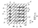
도 1은 본 개시의 실시형태 1에 따른 배선 기판(10)의 일부를 나타내는 종단면도이다. 도 2a는 배선 기판(10)의 제 1 면(S1)의 평면도이다. 도 2b는 배선 기판(10)의 B-B선에 있어서의 단면도이다. 도 2c는 배선 기판(10)의 C-C선에 있어서의 단면도이다.1 is a longitudinal sectional view showing a part of a
실시형태 1의 배선 기판(10)은 제 1 면(S1)과 제 1 면(S1)의 반대측의 제 2 면(S2)을 갖는 절연 기판(11)과, 절연 기판(11)에 위치하는 배선 도체(20) 및 접속 도체(30)를 구비한다. 도면에서는 배선 도체(20)와 접속 도체(30)에 다른 해칭이 나타내어져 있지만, 배선 도체(20)와 접속 도체(30)는 동일한 소재를 갖고, 일체화된 구성이어도 좋다. 배선 기판(10)은 또한, 내부에 복수의 배선층(제 1 배선층(J1)∼제 4 배선층(J4))을 갖는다. 제 1 면(S1) 및 제 2 면(S2)에 위치하는 배선 도체의 층도 배선층이라고 불러도 좋다.A
절연 기판(11)은 세라믹 재료로 구성되는 제 1 절연 기판(11A)과, 수지재료로 구성되는 제 2 절연 기판(11B)을 갖는다. 제 1 절연 기판(11A)과 제 2 절연 기판(11B)은 적층되어 있다. 또한, 절연 기판(11)의 재료는 상기 예에 한정되지 않고, 어떤 재료이어도 좋다. 또한, 절연 기판(11)은 다른 2개의 재료로 구성되는 2개의 기판이 적층된 구성일 필요는 없고, 단일의 재료로 구성된 기판이어도 좋다.The
배선 도체(20)는 전기신호 또는 전압을 전송하는 도체이다. 배선 도체(20)는 제 1 면(S1)에 위치하는 복수의 전극 패드(21, 21t)와, 제 2 면(S2)에 위치하는 복수의 전극(25)과, 제 1 배선층(J1)∼제 4 배선층(J4)에 위치하는 막도체(22)와, 제 1 면(S1), 제 1 배선층(J1)∼제 4 배선층(J4) 및 제 2 면(S2)의 층간에 위치하는 비아 도체(23)를 갖는다. 제 1 배선층(J1)∼제 3 배선층(J3)은 제 2 절연 기판(11B) 내에 위치한다. 제 4 배선층(J4)은 제 1 절연 기판(11A)과 제 2 절연 기판(11B) 사이에 위치한다. 제 1 배선층(J1)∼제 4 배선층(J4)은 제 1 면(S1)에 가까운 쪽부터 이 순서대로 배열된다. 또한, 배선층의 총수는 상기 예에 한정되지 않는다. 또한, 제 1 절연 기판(11A) 내에 1개 또는 복수의 배선층이 위치해도 좋다.The
배선 도체(20)의 막도체(22)에는 접지 전위, 전원 전위 등의 소정 전위가 공급되는 솔리드형상 도체(24)가 포함된다. 솔리드형상 도체(24)란 배선 기판(10) 중 배선 도체(20)가 배치되는 영역(배선 도체(20)가 배치되지 않는 주변부를 제외한 영역) 중 30% 이상의 면적에 퍼지는 도체를 의미한다. 솔리드형상 도체(24)는 비아 도체(23)를 통과시키는 관통 구멍, 어떤 영역을 피하는 슬릿 또는 노치를 갖고 있어도 좋다. 솔리드형상 도체(24)는 본 개시에 따른 제 1 솔리드형상 도체의 일례에 상당한다.The
전극 패드(21, 21t)는 전해 도금이 실시되어 있다. 전해 도금은 예를 들면 1㎛∼10㎛ 정도의 니켈막과 0.1㎛∼3㎛ 정도의 금막이 순서대로 적층된 구성이어도 좋다. 전해 도금에 의해, 전극 패드(21, 21t)의 표면을 보호하고, 또한, 납재, 땜납 등의 접합성을 높일 수 있다. 복수의 전극 패드(21, 21t)는 배선 도체(20)를 통해 반대측의 복수의 전극(25) 중 어느 하나와 도통하고 있는 것과, 배선 도체(20)를 통해 어느 전극(25)와도 도통하지 않는 것이 포함되어 있어도 좋다. 반대측의 어느 전극(25)과 도통하지 않는 전극 패드(21t), 또는 전극(25)과의 사이의 저항이 높은 전극 패드(21t)는 그 상태에서는 전해 도금시에 반대측의 전극(25)으로부터 충분한 전류를 받을 수 없다.The
접속 도체(30)는 전극 패드(21, 21t)의 전해 도금시에, 배선 도체(20)만으로부터 전류를 받을 수 없거나 또는 충분한 전류를 받을 수 없는 전극 패드(21t)에 전류를 공급한 도체이다. 접속 도체(30)는 제 1 배선층(J1)에 위치하는 막도체(32)와, 제 1 배선층(J1)과 제 2 배선층(J2) 사이에 개재하는 비아 도체(33)를 포함한다. 이하, 전해 도금시에 접속 도체(30)를 통해 전류가 공급된 전극 패드(21t)를 「대상 전극 패드(21t)」라고도 기재한다. 배선 도체(20)에는 복수의 대상 전극 패드(21t)가 포함되어 있어도 좋다.The
배선 기판(10)은 또한, 일부가 절취된 홈(X)을 갖는다. 홈(X)은 레이저 빔에 의해 일부가 절취된 자국이지만, 전자 빔 등의 다른 빔에 의해 일부가 절취된 자국이어도 좋다. 홈(X)은 절연 물질에 의해 메워져 있어도 좋다.The
<대상 전극 패드, 접속 도체, 솔리드형상 도체 및 홈의 배치 관계><Arrangement relationship of target electrode pad, connection conductor, solid conductor and groove>
대상 전극 패드(21t)는 도 2a에 나타낸 바와 같이, 제 1 면(S1)에 위치한다. 또한, 제 1 면(S1)에는 전해 도금시에 접속 도체(30)를 통하지 않고 전류가 공급되는 전극 패드(21)가 위치한다. 도 2a 및 도 2b는 이웃하는 2개의 대상 전극 패드(21t)가 배선층(J1)의 배선 도체(20)를 통해 도통하고 있는 예를 나타내지만, 복수의 대상 전극 패드(21t)는 서로 비도통이어도 좋고, 도 2a 및 도 2b와는 다른 조합으로 도통하고 있어도 좋다.As shown in FIG. 2A, the
접속 도체(30)의 막도체(32)는 도 2b에 나타낸 바와 같이, 제 1 접속 도체(30a)와, 제 2 접속 도체(30b)와, 제 1 접속 도체(30a)와 제 2 접속 도체(30b) 사이에 위치하는 교차부(34)를 포함한다. 도 2b에서는 1개의 제 1 접속 도체(30a)와 1개의 제 2 접속 도체(30b)에만 부호를 붙이고 있지만, 복수의 접속 도체(30)에 마찬가지로 제 1 접속 도체(30a)와 제 2 접속 도체(30b)가 포함된다. 막도체(32)는 배선 도체(20)의 막도체(22)에 접속됨으로써, 대상 전극 패드(21t)에 도통한다. 접속 도체(30)의 각 막도체(32)는 선상이어도 좋다. 교차부(34)는 홈(X)과 교차한다. 그리고, 제 1 접속 도체(30a)가 배선 도체(20)를 통해 대상 전극 패드(21t)와 도통하고, 제 2 접속 도체(30b)가 비아 도체(33)를 통해 솔리드형상 도체(24)에 접속된다. 교차부(34)에 있어서 선상의 막도체(32)는 절단되어 있고, 각 막도체(32)에 있어서 교차부(34)를 사이에 둔 일방과 타방은 도통하지 않는다.As shown in FIG. 2B, the
솔리드형상 도체(24)는 도 2c에 나타낸 바와 같이, 제 2 배선층(J2)에 위치하고, 평면 투시에서, 접속 도체(30)의 막도체(32)와 겹친다. 「평면 투시」란 제 1 면(S1)에 수직인 방향으로부터 내부를 투시한 평면에 상당한다. 이후의 「평면 투시」에 대해서도 마찬가지이다. 솔리드형상 도체(24)는 홈(X)이 교차한 슬릿을 갖고 있어도 좋다. 도시를 생략하지만, 솔리드형상 도체(24)는 도 1의 단면 위치와 다른 개소의 전극(25)에 전기적으로 접속되어 있다.As shown in FIG. 2C, the
홈(X)은 제 1 면(S1)에 개구부를 갖는다. 홈(X)의 바닥은 실시형태 1의 예에서는 제 2 배선층(J2)의 아래에 위치한다. 평면 투시에서, 1개의 홈(X)이 접속 도체(30)의 복수의 막도체(32)와 교차하도록 연장되어 있어도 좋고, 1개의 홈(X)이 접속 도체(30)의 1개의 막도체(32)와만 교차하도록 복수의 홈(X)이 위치하고 있어도 좋다.The groove X has an opening in the first surface S1. The bottom of the groove X is located under the second wiring layer J2 in the example of
홈(X)은 바닥의 위치에 대해서 허용폭을 갖는다. 바닥의 위치의 허용폭은 제 1 배선층(J1)과 제 2 배선층(J2) 사이의 깊이부터, 제 2 배선층(J2)과 제 3 배선층(J3) 사이의 깊이까지이다.The groove (X) has an allowable width with respect to the position of the floor. The allowable width of the bottom position is from the depth between the first wiring layer J1 and the second wiring layer J2 to the depth between the second wiring layer J2 and the third wiring layer J3.
<제조 방법><Manufacturing method>
계속해서, 배선 기판(10)의 제조 방법의 일례에 대해서 설명한다. 제 1 절연 기판(11A)과, 상기 기판에 위치하는 배선 도체(20)는 세라믹 소재의 소성, 및, 메탈라이즈 도체에 의해 형성할 수 있다.Subsequently, an example of a manufacturing method of the
제 2 절연 기판(11B)은 예를 들면, 복수의 수지층을 적층함으로써 형성된다. 수지층은 예를 들면, 폴리이미드 수지, 폴리아미드이미드 수지, 실록산 변성 폴리아미드이미드 수지, 실록산 변성 폴리이미드 수지, 폴리페닐렌설파이드 수지, 전방향족 폴리에스테르 수지, BCB(벤조시클로부텐) 수지, 에폭시 수지, 비스말레이미드트리아진 수지, 폴리페닐렌에테르 수지, 폴리퀴놀린 수지, 불소수지 등의 절연 수지로 이루어지는 것이다. 수지층은 또한, 성형성이나 열팽창계수의 조정을 위해서 필러를 포함하는 것이어도 좋다. 필러로서는 예를 들면, 황산 바륨, 티타늄산 바륨, 무정형 실리카, 결정성 실리카, 용융 실리카, 구상 실리카, 탤크, 클레이, 탄산 마그네슘, 탄산 칼슘, 산화 알루미늄, 수산화 알루미늄, 질화 규소, 질화 알루미늄, 질화 붕소, 알루미나, 산화 마그네슘, 수산화 마그네슘, 산화 티타늄, 마이카, 탤크, 노이부르그 규토(Neuburg silica), 유기 벤토나이트, 인산 지르코늄 등의 무기 필러를 들 수 있다. 수지층은 상기 중 1종류의 필러를 단독으로, 또는 2종류 이상의 필러를 적당히 조합해서 포함하고 있어도 좋다.The second
제 2 절연 기판(11B)의 1개의 수지층은 수지 필름을 아래 층에 접착함으로써 구성해도 좋고, 또는 액상의 전구체 수지를 아래 층에 도포 및 경화시켜서 구성해도 좋다. 1개의 수지층을 형성하면, 상기 수지층 상에 비아 도체(23) 및 막도체(22)에 대응하는 개구를 갖는 레지스트막을 형성하고, 그 후, 에칭 가공 또는 레이저 가공에 의해 막도체(22)에 대응하는 오목부 및 비아 도체(23)에 대응하는 관통 구멍을 형성한다. 이어서, 증착법이나 스퍼터링법, 이온 플레이팅법 등의 박막 형성법에 의해, 수지층의 오목부 및 관통 구멍 내에, 예를 들면 크롬(Cr)-구리(Cu) 합금층, 또는 티타늄(Ti)-구리(Cu) 합금층으로 이루어지는 하지 도체층을 형성한다. 그 후, 도금 등으로 구리, 금 등의 금속으로 오목부 및 관통 구멍을 메우고, 그 후, 레지스트를 박리함으로써, 1개의 수지층과 상기 수지층에 위치하는 배선 도체(20) 또는 접속 도체(30)를 형성할 수 있다. 그리고, 이러한 수지층 및 배선 도체(20) 또는 접속 도체(30)의 형성을 반복하고, 복수의 수지층과 복수의 수지층에 위치하는 배선 도체(20) 또는 접속 도체(30)를 형성한다. 또한, 반복의 마지막의 수지층(최상의 수지층) 위에는 전극 패드(21)에 대응하는 개구를 갖는 레지스트막을 형성하고, 상기 개구에 상기와 동일한 박막 형성법에 의해 하지 도체층을 형성한다. 그리고, 전극 패드(21)의 하지 도체층에, 전해 도금에 의해 니켈막 및 금막을 형성한다.One resin layer of the second insulating
전해 도금시에는 제 1 절연 기판(11A)의 전극(25)으로부터 배선 도체(20) 및 접속 도체(30)를 통해 하지 도체층에 전류를 흘린다. 그리고, 전해 도금이 완료되어 레지스트를 박리하면, 제 1 절연 기판(11A)과 제 2 절연 기판(11B)이 적층된 기판이 형성된다. 이 단계의 기판에 있어서는 접속 도체(30)를 통해 대상 전극 패드(21t)와 배선 도체(20)의 불필요한 도통이 혼재하고 있다. 불필요란 배선 기판(10)의 사용시에 불필요하다라는 의미이다.In the case of electrolytic plating, current flows from the
따라서, 이어서, 상기 불필요한 도통을 제거하기 위해서, 절연 기판(11)의 제 1 면(S1)측으로부터 레이저 빔을 조사해서 접속 도체(30)를 절단하는 가공, 즉 레이저 트리밍 가공을 행한다. 상기 레이저 트리밍 가공에 의해, 제 1 면(S1)에 개구부를 갖는 홈(X), 및, 접속 도체(30)와 홈(X)이 교차한 교차부(34)가 형성되고, 접속 도체(30)가 교차부(34)의 부분에서 절단된다. 그리고, 불필요한 도통이 모두 제거됨으로써, 배선 기판(10)이 제작된다.Therefore, next, in order to remove the unnecessary conduction, a laser beam is irradiated from the side of the first surface S1 of the insulating
이상과 같이, 실시형태 1의 배선 기판(10)에 의하면, 대상 전극 패드(21t)와, 제 2 배선층(J2)에 위치하는 솔리드형상 도체(24)와, 제 1 배선층(J1)에서 홈(X)과 교차하는 교차부(34)를 갖는 접속 도체(30)를 구비한다. 또한, 접속 도체(30)는 제 1 접속 도체(30a)와 제 2 접속 도체(30b)를 포함하고, 제 1 접속 도체(30a)와 제 2 접속 도체(30b) 사이에 교차부(34)가 위치한다. 그리고, 제 2 접속 도체(30b)가 솔리드형상 도체(24)에 도통하고, 제 1 접속 도체(30a)가 대상 전극 패드(21t)에 도통한다. 따라서, 홈(X)의 형성전에, 접속 도체(30)를 통해 전극 패드(21)에 전류를 공급함으로써 전극 패드(21)에 충분한 전해 도금을 행할 수 있고, 그 후, 빔 등에 의해 절연 기판(11)에 홈(X)을 형성함으로써, 접속 도체(30)를 절단해서 배선 도체(20)의 소망의 배선 패턴이 얻어진다.As described above, according to the
또한, 실시형태 1의 배선 기판(10)에 의하면, 홈(X)의 개구부는 제 1 면(S1)에 위치하고, 접속 도체(30)와 홈(X)의 교차부(34)는 제 1 면(S1) 아래의 제 1 배선층(J1)에 위치하고, 솔리드형상 도체(24)는 제 1 배선층(J1) 아래의 제 2 배선층(J2)에 위치한다. 따라서, 접속 도체(30)를 절단하는 홈(X)이 제 2 배선층(J2)까지 도달한 경우라도, 솔리드형상 도체(24)에 슬릿이 형성되는 것뿐이므로, 배선 도체(20)의 전기 특성에 큰 영향이 생기지 않는다. 따라서, 접속 도체(30)를 절단하는 홈(X)의 깊이의 허용값을 크게 채용할 수 있다. 따라서, 접속 도체(30)를 절단하는 공정으로서, 홈(X)의 깊이에 대해서 비교적으로 큰 허용값을 요하는 공정이어도, 번잡함이 저감되는 공정을 채용할 수 있다. 그리고, 상기 공정이 채용됨으로써, 번잡함이 저감되고 또한 높은 신뢰성을 갖고 접속 도체(30)가 절단된 배선 기판(10)을 제공할 수 있다. Further, according to the
또한, 실시형태 1의 배선 기판(10)에 의하면, 홈(X)은 레이저 등의 빔에 의해 절취된 자국이다. 빔을 사용해서 접속 도체(30)를 절단하는 트리밍 가공은 적은 번잡함으로 고속 처리가 가능하다. 따라서, 상기 홈(X)을 갖는 배선 기판(10)은 번잡함이 저감되고 또한 높은 신뢰성을 갖고 접속 도체(30)가 절단된 배선 도체(20)를 구비하는 것이 된다.Further, according to the
(실시형태 2)(Embodiment 2)
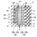
도 3은 본 개시의 실시형태 2에 따른 배선 기판의 일부를 나타내는 종단면도이다. 도 4a는 도 3의 배선 기판의 제 1 면(S1)의 평면도이다. 도 4b는 도 3의 배선 기판의 B-B선에 있어서의 단면도이다. 도 4c는 도 3의 배선 기판의 C-C선에 있어서의 단면도이다. 도 4d는 도 3의 배선 기판의 D-D선에 있어서의 단면도이다.3 is a longitudinal sectional view showing a part of a wiring board according to
실시형태 2의 배선 기판(10A)은 배선 도체(20) 및 접속 도체(30)의 패턴이 상이한 것 외는 실시형태 1의 배선 기판(10)과 거의 같다. 실시형태 2의 배선 기판(10A)에 있어서는 도 4a에 나타낸 바와 같이, 복수의 대상 전극 패드(21ta, 21tb)가 제 1 면(S1)에 위치한다. 복수의 대상 전극 패드(21ta, 21tb)는 배치 영역마다, 도 4a의 지면상 좌측에 위치하는 제 1 군의 대상 전극 패드(21ta)와, 지면상 우측에 위치하는 제 2 군의 대상 전극 패드(21tb)로 구분되어도 좋다.The
접속 도체(30)는 도 4b에 나타낸 바와 같이, 제 1 배선층(J1)에 위치하는 띠형상의 공통 도체(32A)와, 제 1 배선층(J1)에 위치하는 복수의 선형상 도체(32B)를 포함한다. 띠형상이란 선형상 도체(32B)와 비교해서 평면에 있어서의 폭 방향의 치수가 큰 형상을 의미한다. 공통 도체(32A)는 복수의 비아 도체(33)를 통해 제 1 솔리드형상 도체(24A)에 접속되어 있다(도 3을 참조). 공통 도체(32A)는 평면 투시에서 제 1 군의 대상 전극 패드(21t)와 제 2 군의 대상 전극 패드(21t) 사이에 배치된다. 공통 도체(32A)는 제 1 군의 대상 전극 패드(21ta)가 연결되는 방향, 또는 제 2 군의 대상 전극 패드(21tb)가 연결되는 방향을 따라, 길이 방향이 연장되도록 배치되어도 좋다.As shown in FIG. 4B, the
홈(X)은 평면 투시에서, 공통 도체(32A)와 제 1 군의 대상 전극 패드(21ta) 사이와, 공통 도체(32A)와 제 2 군의 대상 전극 패드(21tb) 사이에 위치한다. 홈(X)은 길이 방향이 공통 도체(32A)의 길이 방향을 따라 연장되도록 배치되어도 좋다.Grooves X are located between the
복수의 선형상 도체(32B)의 각각은 제 1 선형상 도체(32Ba)와, 제 2 선형상 도체(32Bb)와, 홈(X)과 교차하는 교차부(34)를 포함한다. 도 4b에서는 2개의 제 1 선형상 도체(32Ba)와 2개의 제 2 선형상 도체(32Bb)에만 부호를 붙이고 있지만, 복수의 선형상 도체(32B)에 마찬가지로 제 1 선형상 도체(32Ba)와 제 2 선형상 도체(32Bb)가 포함된다. 교차부(34)는 제 1 선형상 도체(32Ba)와 제 2 선형상 도체(32Bb) 사이에 위치한다. 그리고, 제 2 선형상 도체(32Bb)가 공통 도체(32A)에 접속되고, 제 1 선형상 도체(32Ba)가 배선 도체(20)(막도체(22) 및 비아 도체(23))를 통해 대상 전극 패드(21ta, 21tb)에 도통한다. 1개의 제 1 선형상 도체(32Ba)가 복수의 대상 전극 패드(21tb)에 도통되어도 좋고, 복수의 제 1 선형상 도체(32Ba)가 1개의 대상 전극 패드(21ta)에 도통되어도 좋다.Each of the plurality of
배선 도체(20)는 도 4c에 나타낸 바와 같이, 제 2 배선층(J2)에 위치하는 제 1 솔리드형상 도체(24A)를 구비한다. 제 1 솔리드형상 도체(24A)는 평면 투시에 있어서, 홈(X)(또는 선형상 도체(32B)의 교차부(34))과 겹치는 개구(M1)를 갖는다. 또한, 배선 도체(20)는 도 4d에 나타낸 바와 같이, 제 3 배선층(J3)에, 평면 투시에 있어서, 홈(X)과 겹치는 부분에 위치하는 제 2 솔리드형상 도체(24B)를 구비해도 좋다.As shown in FIG. 4C, the
실시형태 2의 배선 기판(10A)은 배선 도체(20) 및 접속 도체(30)의 패턴을 다르게 해서, 실시형태 1과 같은 방법에 의해 제조할 수 있다.
실시형태 2의 배선 기판(10A)에 의하면, 접속 도체(30)에 공통 도체(32A)가 포함되므로, 접속 도체(30)의 종합적인 저항이 작아지고, 홈(X)이 형성되기 전의 전해 도금시에 접속 도체(30)를 통해 대상 전극 패드(21ta, 21tb)에 안정된 전류를 공급할 수 있다. 따라서, 대상 전극 패드(21ta, 21tb)에 소정 두께의 도금 피막을 용이하게 형성할 수 있고, 다른 전극 패드(21)와의 두께 불균일도 저감할 수 있다.According to the
또한, 실시형태 2의 배선 기판(10A)에 의하면, 대상 전극 패드(21ta)에 접속되는 선형상 도체(32B)가 길어지고, 접속 도체(30)의 저항이 커지는 경우에는 1개의 대상 전극 패드(21ta)에 복수의 선형상 도체(32B)(복수의 제 1 선형상 도체(32Ba))가 접속된다. 상기 접속에 의해, 대상 전극 패드(21ta)에 접속 도체(30)를 통해 안정된 전류를 공급할 수 있고, 대상 전극 패드(21ta)에 소정 두께의 도금 피막을 용이하게 형성할 수 있고, 다른 전극 패드(21) 및 다른 전극 패드(21tb)와의 두께 불균일을 저감할 수 있다.Further, according to the
또한, 실시형태 2의 배선 기판(10A)에 의하면, 제 1 솔리드형상 도체(24A)가 평면 투시에서 접속 도체(30)의 교차부(34)와 겹치는 개구(M1)를 갖는다. 따라서, 접속 도체(30)를 절단하는 트리밍 가공시에, 절단 에너지(레이저 트리밍 가공이면 레이저 에너지)가 제 1 솔리드형상 도체(24A)에 흡수되기 어렵게 할 수 있다. 따라서, 에너지 부족으로 접속 도체(30)의 절단 불량이 생겨 버리는 것을 저감할 수 있다.Further, according to the
또한, 실시형태 2의 배선 기판(10A)에 의하면, 평면 투시에서 제 1 솔리드형상 도체(24A)의 개구(M1)와 겹치는 제 2 솔리드형상 도체(24B)가 제 3 배선층(J3)에 위치한다. 따라서, 접속 도체(30)를 절단하는 트리밍 가공에 있어서, 홈(X)의 깊이가 제 3 배선층(J3)까지 도달해도, 배선 도체(20)의 전기 특성에 큰 영향이 발생하지 않는다. 따라서, 접속 도체(30)를 절단하는 홈(X)의 깊이의 허용값을 보다 크게 채용할 수 있다. 또한, 제 2 배선층(J2)의 제 1 솔리드형상 도체(24A)가 개구(M1)를 가짐으로써 홈(X)의 깊이의 제어가 어렵게 된 경우라도, 홈(X)의 깊이의 허용값을 보다 크게 할 수 있는 점에서, 홈(X)의 깊이를 허용 범위에 포함시켜서 높은 신뢰성을 갖고 접속 도체(30)를 절단할 수 있다.Further, according to the
(변형예)(modified example)
도 5는 변형예의 배선 기판을 나타내는 단면도이다. 도 5는 도 3의 C-C선에 있어서의 단면도를 나타낸다. 변형예의 배선 기판(10B)은 제 2 배선층(J2)의 배선 도체(20) 이외는 실시형태 2와 같다.5 is a cross-sectional view showing a wiring board of a modified example. FIG. 5 shows a cross-sectional view taken along line C-C in FIG. 3 . The
변형예의 배선 기판(10B)은 제 2 배선층(J2)의 제 1 솔리드형상 도체(24A)에, 평면 투시에서, 홈(X)(또는 선형상 도체(32B)의 교차부(34))과 겹치는 개구(M1)를 갖는다. 또한, 제 2 배선층(J2)의 배선 도체(20)는 개구(M1) 내에 위치하고, 홈(X)(또는 선형상 도체(32B)의 교차부(34))과 겹치는 도체편(N1)을 갖는다. 도체편(N1)은 제 1 솔리드형상 도체(24A)와 비도통의 플로팅 도체이어도 좋고, 제 1 솔리드형상 도체(24A)와 일부가 접속된 도체이어도 좋다.The
변형예의 배선 기판(10B)에 의하면, 제 1 솔리드형상 도체(24A)의 개구(M1)에 의해, 접속 도체(30)를 절단하는 트리밍 가공시에, 절단 에너지(레이저 트리밍 가공이면 레이저 에너지)가 제 1 솔리드형상 도체(24A)에 흡수되기 어렵게 할 수 있다. 따라서, 에너지 부족으로 접속 도체(30)의 절단 불량이 생겨 버리는 것을 저감할 수 있다. 또한, 변형예의 배선 기판(10B)에 의하면, 개구(M1) 내에, 홈(X)과 겹치는 도체편(N1)을 갖는다. 도체편(N1)은 제 1 솔리드형상 도체(24A)와 접속되어있지 않거나, 또는 일부밖에 접속되어 있지 않으므로, 접속 도체(30)를 절단하는 트리밍 가공시에, 절단 에너지(레이저 트리밍 가공이면 레이저 에너지)가 열전도 등에 의해 도체편(N1)으로부터 제 1 솔리드형상 도체(24A)로 방출되어 흡수하기 어렵게 할 수 있다. 또한, 가령, 트리밍 가공시에, 절단 에너지가 제 2 배선층(J2)에 도달한 경우라도, 절단 에너지가 도체편(N1)의 절단에 사용됨으로써, 절단 에너지가 더 아래의 제 3 배선층(J3)에 도달하기 어렵게 할 수 있다. 따라서, 트리밍 가공에 의해 배선 도체(20)의 전기 특성에 영향이 생기기 어렵게 할 수 있으면서, 높은 신뢰성을 갖고 접속 도체(30)가 절단된 배선 기판(10B)을 제공할 수 있다. 변형예에 있어서는 제 1 솔리드형상 도체(24A) 아래의 배선층(제 3 배선층(J3))에, 평면 투시에서, 제 1 솔리드형상 도체(24A)의 개구(M1)와 겹치는 선형상의 막도체(22)가 배치되어도, 상기 막도체(22)가 홈(X)에 의해 절단되어 버릴 우려는 저감된다.According to the
(프로브 카드)(probe card)
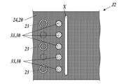
도 6a는 본 개시의 실시형태에 따른 프로브 카드를 나타내는 평면도이다. 도 6b는 본 개시의 실시형태에 따른 프로브 카드를 나타내는 종단면도이다. 본 실시형태의 프로브 카드(100)는 복수의 반도체 소자가 형성된 반도체 웨이퍼(SW)의 시험 장치에 장착되는 구성부품이다. 본 실시형태의 프로브 카드(100)는 배선 기판(10)과, 배선 기판(10)의 복수의 전극 패드(21, 21t)에 접속된 복수의 프로브 핀(40)을 구비한다.6A is a plan view illustrating a probe card according to an embodiment of the present disclosure. 6B is a longitudinal cross-sectional view illustrating a probe card according to an embodiment of the present disclosure. The
프로브 핀(40)은 니켈, 텅스텐 등의 금속으로 구성되고, 땜납 등의 도전성의 접합재를 통해 전극 패드(21, 21t)에 접합된다. 프로브 카드(100)는 시험용의 신호 또는 전압을 입출력하는 신호 처리 회로와, 시험 대상의 반도체 웨이퍼(SW) 사이에 개재해서 복수의 프로브 핀(40)이 반도체 소자의 전극에 접촉한다.The
프로브 카드(100)의 배선 기판(10)으로서는 실시형태 1의 구성이 적용되는 외에, 실시형태 2의 배선 기판(10A), 또는 변형예의 배선 기판(10B)이 적용되어도 좋다. 배선 기판(10)의 제 1 절연 기판(11A)은 도 6b에 나타낸 바와 같이, 복수의 절연층이 적층되어서 구성되고, 내부에 비아 도체(23)에 추가해서 배선층이 되는 막도체(22)가 포함되어 있어도 좋다. 또한, 제 1 절연 기판(11A)에는 히터선(50)이 포함되어 있어도 좋다.As the
본 실시형태의 프로브 카드에 의하면, 배선 기판(10)의 전극 패드(21, 21t)가 안정된 두께의 피막을 갖는다. 따라서, 프로브 핀(40)을 안정적으로 접합할 수 있어 프로브 핀(40)의 접합부에 대한 신뢰성을 향상시킬 수 있다.According to the probe card of this embodiment, the
이상, 본 개시의 각 실시형태에 대해서 설명했다. 그러나, 본 개시의 배선 기판 및 프로브 카드는 상기 실시형태에 한정되는 것은 아니다. 예를 들면, 상기 실시형태에서는 배선 기판의 용도로서 프로브 카드의 배선 기판을 나타냈지만, 전자소자, 전기소자 또는 여러가지 전기 회로가 탑재되는 배선 기판에 본 개시의 배선 기판이 적용되어도 좋다. 또한, 상기 실시형태에서는 전극 패드가 위치하는 면에 홈의 개구부가 위치하는 예를 나타냈지만, 전극 패드는 다른 면에 위치해도 좋다. 또한, 상기 실시형태에서는 접속 도체와 홈이 교차하는 교차부가 위치하는 제 1 배선층이, 홈의 개구부가 위치하는 제 1 면의 아래에 위치하는 예를 나타냈지만, 교차부가 위치하는 제 1 배선층은 홈의 개구부가 위치하는 제 1 면에 위치하고 있어도 좋다. 그 외, 실시형태에서 나타낸 세부는 발명의 취지를 일탈하지 않는 범위에서 적당히 변경 가능하다.In the above, each embodiment of the present disclosure has been described. However, the wiring board and probe card of the present disclosure are not limited to the above embodiments. For example, in the above embodiment, the wiring board of the probe card is shown as the use of the wiring board, but the wiring board of the present disclosure may be applied to a wiring board on which electronic elements, electric elements, or various electric circuits are mounted. Further, in the above embodiment, an example in which the opening of the groove is located on the surface where the electrode pad is located has been shown, but the electrode pad may be located on another surface. Further, in the above embodiment, an example was shown in which the first wiring layer in which the intersection portion where the connecting conductor and the groove intersect is located is located below the first surface where the opening of the groove is located, but the first wiring layer in which the intersection portion is located is located in the groove It may be located on the first surface where the opening of is located. In addition, the details shown in the embodiments can be appropriately changed within a range not departing from the spirit of the invention.
(산업상 이용가능성)(industrial applicability)
본 개시는 배선 기판 및 프로브 카드에 이용할 수 있다.The present disclosure can be used for wiring boards and probe cards.
10, 10A, 10B: 배선 기판
11: 절연 기판
S1: 제 1 면
S2: 제 2 면
20: 배선 도체
21, 21t, 21ta, 21tb: 전극 패드
22: 막도체
23: 비아 도체
24: 솔리드형상 도체
24A: 제 1 솔리드형상 도체
M1: 개구
N1: 도체편
24B: 제 2 솔리드형상 도체
25: 전극
30: 접속 도체
30a: 제 1 접속 도체
30b: 제 2 접속 도체
32: 막도체
32A: 공통 도체
32B: 선형상 도체
32Ba: 제 1 선형상 도체
32Bb: 제 2 선형상 도체
33: 비아 도체
34: 교차부
X: 홈
J1: 제 1 배선층
J2: 제 2 배선층
J3: 제 3 배선층
J4: 제 4 배선층
100: 프로브 카드10, 10A, 10B: wiring board
11: insulating substrate
S1: first side
S2: 2nd side
20: wiring conductor
21, 21t, 21ta, 21tb: electrode pad
22: film conductor
23 via conductor
24: Solid shape conductor
24A: first solid conductor
M1: opening
N1: conductor piece
24B: second solid conductor
25: electrode
30: connecting conductor
30a: first connecting conductor
30b: second connecting conductor
32 film conductor
32A: common conductor
32B: linear phase conductor
32Ba: first linear phase conductor
32Bb: second linear phase conductor
33 via conductor
34: intersection
X: home
J1: first wiring layer
J2: second wiring layer
J3: third wiring layer
J4: 4th wiring layer
100: probe card
Claims (8)
상기 절연 기판에 위치하는 배선 도체 및 접속 도체와,
상기 배선 도체의 일부가 포함되는 제 1 배선층 및 제 2 배선층과,
상기 제 1 면에 개구부를 갖는 홈을 구비하고,
상기 배선 도체는,
전극 패드와,
상기 제 2 배선층에 포함되는 제 1 솔리드형상 도체를 갖고,
상기 접속 도체는 제 1 접속 도체와, 제 2 접속 도체와, 상기 제 1 배선층에서 상기 홈과 교차한 교차부를 포함하고,
상기 교차부는 상기 제 1 접속 도체와 상기 제 2 접속 도체 사이에 위치하고,
상기 제 1 접속 도체가 상기 전극 패드에 도통되고, 상기 제 2 접속 도체가 상기 제 1 솔리드형상 도체에 도통되고,
상기 제 1 배선층은 상기 제 1 면 또는 상기 제 1 면의 아래에 위치하고, 상기 제 2 배선층은 상기 제 1 배선층의 아래에 위치하는 배선 기판.an insulating substrate having a first surface;
wiring conductors and connecting conductors positioned on the insulating substrate;
a first wiring layer and a second wiring layer containing a part of the wiring conductor;
A groove having an opening is provided on the first surface,
The wiring conductor,
an electrode pad;
a first solid conductor included in the second wiring layer;
The connecting conductor includes a first connecting conductor, a second connecting conductor, and an intersection portion intersecting the groove in the first wiring layer,
The crossing portion is located between the first connection conductor and the second connection conductor,
the first connection conductor is conductive to the electrode pad, and the second connection conductor is conductive to the first solid conductor;
The first wiring layer is positioned on or under the first surface, and the second wiring layer is positioned under the first wiring layer.
상기 홈은 빔에 의해 절취된 자국인 배선 기판.According to claim 1,
The wiring board of claim 1 , wherein the groove is a mark cut by a beam.
복수의 상기 전극 패드를 갖고,
상기 접속 도체는 상기 제 1 배선층에 위치하는 복수의 선형상 도체와, 상기 제 1 배선층에 위치하는 띠형상의 공통 도체를 포함하고,
상기 복수의 선형상 도체의 각각이 제 1 선형상 도체와, 제 2 선형상 도체와, 상기 제 1 선형상 도체와 상기 제 2 선형상 도체 사이에 위치하는 상기 교차부를 포함하고,
상기 각각의 선형상 도체의 상기 제 1 선형상 도체가 상기 복수의 전극 패드 중 어느 하나에 도통되고, 상기 각각의 선형상 도체의 상기 제 2 선형상 도체가 상기 공통 도체에 접속되어 있는 배선 기판.According to claim 1 or 2,
having a plurality of the electrode pads;
The connection conductor includes a plurality of linear conductors positioned on the first wiring layer and a strip-shaped common conductor positioned on the first wiring layer;
Each of the plurality of linear conductors includes a first linear conductor, a second linear conductor, and the intersection portion positioned between the first linear conductor and the second linear conductor,
The wiring board according to claim 1 , wherein the first linear conductor of each of the linear conductors is conductive to any one of the plurality of electrode pads, and the second linear conductor of each of the linear conductors is connected to the common conductor.
상기 접속 도체는 1개의 상기 전극 패드에 도통된 복수의 선형상 도체를 포함하는 배선 기판.According to any one of claims 1 to 3,
The wiring board according to claim 1 , wherein the connection conductor includes a plurality of linear conductors conducted to one electrode pad.
상기 제 1 솔리드형상 도체는 평면 투시에서 상기 교차부와 겹치는 개구를 갖는 배선 기판.According to any one of claims 1 to 4,
The wiring board of claim 1 , wherein the first solid conductor has an opening overlapping the intersection portion in plan view.
상기 제 2 배선층의 아래에 위치하는 제 3 배선층과,
상기 제 3 배선층에 위치하고, 평면 투시에서 상기 개구와 겹치는 제 2 솔리드형상 도체를 갖는 배선 기판.According to claim 5,
a third wiring layer positioned below the second wiring layer;
A wiring board having a second solid conductor positioned on the third wiring layer and overlapping the opening in plan view.
상기 배선 도체는,
상기 개구 내에 위치하고 평면 투시에서 상기 교차부와 겹치는 도체편을 포함하는 배선 기판.According to claim 5,
The wiring conductor,
A wiring board comprising a conductor piece positioned within the opening and overlapping the intersection portion in plan view.
상기 배선 기판에 접속된 복수의 프로브 핀을 구비하는 프로브 카드.The wiring board according to any one of claims 1 to 7;
A probe card having a plurality of probe pins connected to the wiring board.
Applications Claiming Priority (3)
| Application Number | Priority Date | Filing Date | Title |
|---|---|---|---|
| JP2020196678 | 2020-11-27 | ||
| JPJP-P-2020-196678 | 2020-11-27 | ||
| PCT/JP2021/043263 WO2022114078A1 (en) | 2020-11-27 | 2021-11-25 | Wiring board and probe card |
Publications (1)
| Publication Number | Publication Date |
|---|---|
| KR20230096042A true KR20230096042A (en) | 2023-06-29 |
Family
ID=81754317
Family Applications (1)
| Application Number | Title | Priority Date | Filing Date |
|---|---|---|---|
| KR1020237017636A KR20230096042A (en) | 2020-11-27 | 2021-11-25 | Wiring board and probe card |
Country Status (4)
| Country | Link |
|---|---|
| US (1) | US20240027493A1 (en) |
| JP (1) | JPWO2022114078A1 (en) |
| KR (1) | KR20230096042A (en) |
| WO (1) | WO2022114078A1 (en) |
Family Cites Families (8)
| Publication number | Priority date | Publication date | Assignee | Title |
|---|---|---|---|---|
| JPH0249742Y2 (en) * | 1985-12-09 | 1990-12-27 | ||
| JPS63224392A (en) * | 1987-03-13 | 1988-09-19 | 日本メクトロン株式会社 | Multilayer printed interconnection board and method of processing the same |
| JP3008146B2 (en) * | 1992-10-26 | 2000-02-14 | 株式会社住友金属エレクトロデバイス | Ceramic package for housing semiconductor element and method of manufacturing the same |
| JPH11163500A (en) * | 1997-11-25 | 1999-06-18 | Sumitomo Metal Smi Electron Devices Inc | Cleaning method of ceramic wiring board |
| JP5334607B2 (en) * | 2008-12-25 | 2013-11-06 | 京セラ株式会社 | WIRING BOARD, WIRING BOARD MANUFACTURING METHOD, AND PROBE CARD |
| JP2010232579A (en) * | 2009-03-30 | 2010-10-14 | Oki Networks Co Ltd | Method of manufacturing printed wiring board |
| JP2012243836A (en) * | 2011-05-17 | 2012-12-10 | Hitachi Cable Ltd | Flexible wiring board and manufacturing method of the same |
| CN104427789B (en) * | 2013-08-22 | 2017-09-12 | 鹏鼎控股(深圳)股份有限公司 | Multilayer circuit board and preparation method thereof |
-
2021
- 2021-11-25 WO PCT/JP2021/043263 patent/WO2022114078A1/en active Application Filing
- 2021-11-25 JP JP2022565418A patent/JPWO2022114078A1/ja active Pending
- 2021-11-25 US US18/038,639 patent/US20240027493A1/en active Pending
- 2021-11-25 KR KR1020237017636A patent/KR20230096042A/en unknown
Also Published As
| Publication number | Publication date |
|---|---|
| WO2022114078A1 (en) | 2022-06-02 |
| US20240027493A1 (en) | 2024-01-25 |
| JPWO2022114078A1 (en) | 2022-06-02 |
Similar Documents
| Publication | Publication Date | Title |
|---|---|---|
| US8138609B2 (en) | Semiconductor device and method of manufacturing semiconductor device | |
| US9839132B2 (en) | Component-embedded substrate | |
| KR100659521B1 (en) | Connection structure of inner conductor and multilayer substrate | |
| TW201004504A (en) | Manufacturing method of printed circuit board having electro component | |
| KR101382811B1 (en) | The printed circuit board and the method for manufacturing the same | |
| US20170019985A1 (en) | Suspension board assembly sheet having circuits, method of manufacturing the same and method of inspecting the same | |
| KR20130084033A (en) | Pcb using for semiconductor module | |
| JP2013172137A (en) | Wiring board and probe card using the same | |
| WO2022114078A1 (en) | Wiring board and probe card | |
| US8981237B2 (en) | Wiring board for electronic parts inspecting device and its manufacturing method | |
| US11651904B2 (en) | Multilayer ceramic substrate and probe card including same | |
| JP2012198190A5 (en) | ||
| TW201507555A (en) | Wiring board with hybrid core and dual build-up circuitries | |
| JP2008060208A (en) | Multilayer printed circuit board, and probe card using the same | |
| RU2511054C2 (en) | Method of making semiconductor devices | |
| JP7373471B2 (en) | wiring board | |
| WO2022107225A1 (en) | Probe-card multilayer wiring substrate and probe card | |
| EP0253833B1 (en) | Multilayer printed circuit board | |
| CN112566390B (en) | Multilayer flexible circuit board and preparation method thereof | |
| JP2022014105A (en) | Wiring board | |
| JP2022014122A (en) | Wiring board | |
| JPH06308196A (en) | Test head structure | |
| JP2022178360A (en) | Printed board | |
| KR20220088766A (en) | Circuit boards, boards for probe cards and probe cards | |
| JP2020120048A (en) | Wiring board and electronic apparatus |