EP0253833B1 - Multilayer printed circuit board - Google Patents
Multilayer printed circuit board Download PDFInfo
- Publication number
- EP0253833B1 EP0253833B1 EP19870900434 EP87900434A EP0253833B1 EP 0253833 B1 EP0253833 B1 EP 0253833B1 EP 19870900434 EP19870900434 EP 19870900434 EP 87900434 A EP87900434 A EP 87900434A EP 0253833 B1 EP0253833 B1 EP 0253833B1
- Authority
- EP
- European Patent Office
- Prior art keywords
- circuit board
- printed circuit
- substrates
- elements
- plated
- Prior art date
- Legal status (The legal status is an assumption and is not a legal conclusion. Google has not performed a legal analysis and makes no representation as to the accuracy of the status listed.)
- Expired - Lifetime
Links
Images


Classifications
-
- H—ELECTRICITY
- H05—ELECTRIC TECHNIQUES NOT OTHERWISE PROVIDED FOR
- H05K—PRINTED CIRCUITS; CASINGS OR CONSTRUCTIONAL DETAILS OF ELECTRIC APPARATUS; MANUFACTURE OF ASSEMBLAGES OF ELECTRICAL COMPONENTS
- H05K1/00—Printed circuits
- H05K1/02—Details
- H05K1/11—Printed elements for providing electric connections to or between printed circuits
- H05K1/115—Via connections; Lands around holes or via connections
- H05K1/116—Lands, clearance holes or other lay-out details concerning the surrounding of a via
-
- H—ELECTRICITY
- H05—ELECTRIC TECHNIQUES NOT OTHERWISE PROVIDED FOR
- H05K—PRINTED CIRCUITS; CASINGS OR CONSTRUCTIONAL DETAILS OF ELECTRIC APPARATUS; MANUFACTURE OF ASSEMBLAGES OF ELECTRICAL COMPONENTS
- H05K1/00—Printed circuits
- H05K1/02—Details
- H05K1/0286—Programmable, customizable or modifiable circuits
- H05K1/0287—Programmable, customizable or modifiable circuits having an universal lay-out, e.g. pad or land grid patterns or mesh patterns
- H05K1/0289—Programmable, customizable or modifiable circuits having an universal lay-out, e.g. pad or land grid patterns or mesh patterns having a matrix lay-out, i.e. having selectively interconnectable sets of X-conductors and Y-conductors in different planes
-
- H—ELECTRICITY
- H05—ELECTRIC TECHNIQUES NOT OTHERWISE PROVIDED FOR
- H05K—PRINTED CIRCUITS; CASINGS OR CONSTRUCTIONAL DETAILS OF ELECTRIC APPARATUS; MANUFACTURE OF ASSEMBLAGES OF ELECTRICAL COMPONENTS
- H05K1/00—Printed circuits
- H05K1/02—Details
- H05K1/0286—Programmable, customizable or modifiable circuits
- H05K1/0292—Programmable, customizable or modifiable circuits having a modifiable lay-out, i.e. adapted for engineering changes or repair
-
- H—ELECTRICITY
- H05—ELECTRIC TECHNIQUES NOT OTHERWISE PROVIDED FOR
- H05K—PRINTED CIRCUITS; CASINGS OR CONSTRUCTIONAL DETAILS OF ELECTRIC APPARATUS; MANUFACTURE OF ASSEMBLAGES OF ELECTRICAL COMPONENTS
- H05K2201/00—Indexing scheme relating to printed circuits covered by H05K1/00
- H05K2201/09—Shape and layout
- H05K2201/09209—Shape and layout details of conductors
- H05K2201/09372—Pads and lands
- H05K2201/09381—Shape of non-curved single flat metallic pad, land or exposed part thereof; Shape of electrode of leadless component
-
- H—ELECTRICITY
- H05—ELECTRIC TECHNIQUES NOT OTHERWISE PROVIDED FOR
- H05K—PRINTED CIRCUITS; CASINGS OR CONSTRUCTIONAL DETAILS OF ELECTRIC APPARATUS; MANUFACTURE OF ASSEMBLAGES OF ELECTRICAL COMPONENTS
- H05K2201/00—Indexing scheme relating to printed circuits covered by H05K1/00
- H05K2201/09—Shape and layout
- H05K2201/09209—Shape and layout details of conductors
- H05K2201/09654—Shape and layout details of conductors covering at least two types of conductors provided for in H05K2201/09218 - H05K2201/095
- H05K2201/0979—Redundant conductors or connections, i.e. more than one current path between two points
-
- H—ELECTRICITY
- H05—ELECTRIC TECHNIQUES NOT OTHERWISE PROVIDED FOR
- H05K—PRINTED CIRCUITS; CASINGS OR CONSTRUCTIONAL DETAILS OF ELECTRIC APPARATUS; MANUFACTURE OF ASSEMBLAGES OF ELECTRICAL COMPONENTS
- H05K2201/00—Indexing scheme relating to printed circuits covered by H05K1/00
- H05K2201/10—Details of components or other objects attached to or integrated in a printed circuit board
- H05K2201/10613—Details of electrical connections of non-printed components, e.g. special leads
- H05K2201/10621—Components characterised by their electrical contacts
- H05K2201/10689—Leaded Integrated Circuit [IC] package, e.g. dual-in-line [DIL]
-
- H—ELECTRICITY
- H05—ELECTRIC TECHNIQUES NOT OTHERWISE PROVIDED FOR
- H05K—PRINTED CIRCUITS; CASINGS OR CONSTRUCTIONAL DETAILS OF ELECTRIC APPARATUS; MANUFACTURE OF ASSEMBLAGES OF ELECTRICAL COMPONENTS
- H05K3/00—Apparatus or processes for manufacturing printed circuits
- H05K3/40—Forming printed elements for providing electric connections to or between printed circuits
- H05K3/42—Plated through-holes or plated via connections
- H05K3/429—Plated through-holes specially for multilayer circuits, e.g. having connections to inner circuit layers
Definitions
- the present invention relates to multilayer printed circuit boards.
- Multilayer printed circuit boards are formed of bonded stacks of cards or substrates of insulated material having tracks or lines of printed conduc- torelements located on their surfaces, the conductor elements being formed typically by the deposition of a metal such as copper on appropriate areas on the substrates or by etching away unwanted areas of a metal film such as copper which is bonded to the substrates.
- Each card or substrate may be single or double sided, i.e., having lines of conductor elements on one or on both surfaces of the card.
- Prior printed circuit boards have been designed with a different circuit on each card or substrate, the circuits being placed in overlying positions so that points for electrical connections between the circuits are congruent to each other.
- the individual circuits are then connected by drilling through the assembled cards and plating the holes thus formed with a layer of electrically conductive material such as copper.
- the leads of the circuit components are then mounted within the holes of an exposed planar surface of the assembled board. These leads are then connected with conductor elements on different layers of the board.
- the conductive layers may be designed to provide different power supply potentials to the circuit or to be used for signal transmission. Since the layout design of prior art high density multilayer printed circuit boards is often complex as result of the intricate patterns of the conductors, together with their interconnecting points, it can be a very time consuming and costly procedure to design such layouts.
- a voltage printed circuit board including a plurality of through connections extending through an insulating substrate between first and second spaced parallel planes of the board, the through connections being arranged in a pattern of rows and columns; a plurality of first conductive tracks in said first plane each track extending between adjacent columns of through connections and connected to selected ones of the through connections in one or both columns adjacent thereto; a plurality of second tracks in said second plane and extending between adjacent rows of the through connections and transversely of the firsttracks and connected to selected ones of the through connections in one or both rows adjacent thereto; the arrangement being such that none of the through- connections are connected to more than one track; whereby desired conductor configurations may be provided on the board by inter-connecting selected tracks by conductive links, between through connections which are connected to those selected tracks and where necessary, introducing discontinuities in said tracks.
- a multilayer printed circuit board including a plurality of substrates of electrically insulating material bonded together in a stacked relationship and each having a first surface on which is formed a pattern of electrically conductive material, a plurality of circuit elements mounted on said first surface of an end one of said substrates, and a plurality of plated-through holes extending transversely to the substrates, wherein said pattern of conductive material of each substrate includes a plurality of parallel conductors, a plurality of connecting pads each having a plated through hole passing therethrough and each having a generally square configuration with rounded corners, and a plurality of connecting elements each connecting a corner of an associated connecting pad to an adjacent one of said parallel conductors.
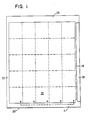
- FIG. 1 there is shown a plan view of the top layer of a multilayer printed circuit board 20 constructed in accordance with the present invention.
- the surface of the top layer of the board 20 comprises a plurality of equal surface areas or "domains" 22 in which preferably there are mounted the same number of I.C. packages.
- the top surfaces of each of the remaining layers of the circuit board have a similar layout of equal domain areas.
- the area 24 of the circuit board 20, located adjacent the upper edge of the circuit board, may accommodate other circuit components.
- the area 25 accommodates connecting pins of the board for connecting the board to other printed circuit boards of the same logic deck while the area 23 accommodates connectors for the logic deck cable connection (not shown).
- the area 21 is designated for test lines (not shown) which are useful in monitoring the quality of the board 20.
- Buffer gates may be located in the area 19 for signal connections to other circuits of the same logic deck.
- a domain area 22 may include a predetermined number of I.C. packages 26 such as dual-in-line packages (DIP) or a Macrocell package 27 which is commercially available from Motorola Corp. of Phoenix, Arizona, U.S.A.
- DIP dual-in-line packages
- Macrocell package 27 which is commercially available from Motorola Corp. of Phoenix, Arizona, U.S.A.
- Each lead element or pin 28 of the DIP packages 26 and the Macrocell package 27 is connected to a monitor point or hole 30 by a 2.5 millimeter copper bridge element 32.
- the monitor holes 30 may also be connected to circuit elements such as connecting pads or conductor elements located within the printed circuit board and are used for testing and repairing the circuit elements in a manner that will be explained more fully hereinafter.
- each domain area 22 of the circuit board is constructed to have the same number of monitor and connecting holes. Also located on the circuit board within each domain area and adjacent each of the I.C. packages 26 (Fig. 2) and 27 (Fig. 3) is a row of holes 38 for mounting passive components associated with the circuit, such as resistors 36, etc.
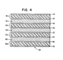
- Fig. 4 there is shown a cross-sectional view of a portion of the printed circuit board 20 of the present invention which is comprised of four double sided copper layer printed circuit cards 40a-40d, inclusive, bonded together in a stacked relationship by layers of dielectric material 42a-42c inclusive.
- the four circuit cards are constructed of an epoxy-glass material while the laminated layers 42a-42c inclusive are of a similar dielectric material.
- An etching process well known in the art provides a pattern of lines comprising conductor elements or foils 62 and connecting pads 72 (Fig. 5A-5C inclusive) in the upper copper layers 44, 48, 52, and 56 (Fig. 4) of cards 40a-40d inclusive.
- Layers 44, 48, 52 and 56 are designated signal layers over which signals associated with the operation of the circuit are transmitted.
- the copper layer 46 (Fig. 4) is connected to a minus 5.2 volts D.C. power supply while the layer 54 is connected to a minus 2 volts D.C. power supply.
- the copper layers 50 and 58 are connected to ground.
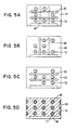
- Figs. 5A-5D inclusive there are shown plan views of portions of the copper layers 44, 58, 52 and 56.
- the arrangement of the conductor elements 62, shown in Figs. 5A-5C inclusive, is intended to maximize the density of the circuit elements in a board using the circuit packages 26 (Fig. 2).
- the top or utility copper layer 44 (Fig. 5A) has lines of parallel conductor elements 62 extending in either the X or Y direction but, in any case the lines may never intersect each other.
- The, conductor elements 62 (Fig. 5B) located in the layers 48 and 56 are parallel and extend in the Y direction while the conductor elements 62 (Fig. 5C) located in the copper layer 52 and parallel and extend in the X direction.
- the conductor elements 62 are arranged so that the domain areas of the signal layers 44, 48, 52 and 56 each contain the same number of conductor elements 62. This uniform arrangement of the conductor elements 62 produces uniform stress and heat dissipation within the board, thus reducing the amount of warpage that may occur.
- the sandwiching of the power layers 46, 50 and 54 (Fig. 4) between the signal layers 44, 48, 52 and 56 further reduces the noise level.
- the lower ground layer 58 (Fig. 5D) includes soldering pads 66 which may be positioned to interconnect plated-through holes 70 with the ground layer 58 through a void or recessed portion 71 (Fig. 8) of the ground layer 58. These connections are made through the use of spoke elements 69 (Fig.
- Each hole 70 may comprise a monitor hole 30 (Fig. 2), a connecting hole 31, or the hole which receives a lead pin from an I.C. package.
- connecting pins 68 Located in certain of the holes 70 are connecting pins 68 (Fig. 8) which are used to interconnect the layers of the printed circuit board by means of connecting pads 72 (Figs. 5A-5C inclusive) in a manner to be described more fully hereafter.
- the connecting pins 68 may comprise the pins of I.C. packages 26, 27 (Figs 2 and 3) or separate pins.
- the pads 72 interconnect pins 68 with other circuit elements and with the copper layers in which the pads are located.
- the inserted pins 68 are soldered to the board 20 through holes 70 and pads 72. Because the pads 72 and the conductor elements 62 have their designated locations in the layers, a pad will never block the way of a conductor element.
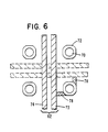
- each of the conductor elements 62 (Figs 5A-5C inclusive) consists of two parallel conductor segments 73, 74 through which electrical signals are transmitted.
- each connecting pad 72 is formed of copper in a generally square configuration having curved corner portions 76.
- Each pad 72 is connected at one of its corner portions 76 to one of the conductor segments 73, or 74 by a connecting element 78 composed of the same material as the conductor elements 62, which in the present embodiment is copper. This arrangement allows the required electrical connection to be made between the pad 72 and the segments 73, 74.
- the splitting of the conductor element 62 into the segments 73 and 74 is made to maintain a constant density of conductor elements which produces less crosstalk between the conductor elements 62 and provides an easier access to any of the pads 72.
- the size of a pad 72 (Fig. 7) must be such that it is possible to make connections to the conductor elements 62 under the worst case conditions of artwork and manufacturing tolerances. It has been found that a square pad, being connected to a connecting element 78 at a curved corner portion, can tolerate a larger hole 70 than a round pad whose diameter is equal to a side of the square pad. Preferably, adjacent corners of a pad 72 are respectively connected to two connecting elements 78.
- a conductor segment 73 or 74 will remain connected with an associated pad in the event that one of the corner portions 76 of the pad is broken off during the off center drilling of the respective hole 70.
- This double connection arrangement provides a way to select a smaller pad for an extremely dense packaging condition.
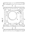
- Fig. 7 shows an off-center drilled hole 70 after it has been plated with a copper layer 37.
- a simplified enlarged cross-sectional view of a portion of the printed circuit board 20 which illustrates the signal path extending between two of the copper layers of the circuit board using the connecting pads 72 and the mounting of a connecting pin 68 within a plated through hole 70.
- the signal may be transmitted from layer 52 through the plated through hole 80a, the layer 44, the plated-through hole 80b, the layer 48, the plated-through hole 80c, layer 44 and the plated-through hole 80d to layer 56.
- a signal path is completed using the connecting pads 72 and the plated-through holes 80a-80d inclusive.
- each of the glass-epoxy cards 40a-40d inclusive (Fig. 4) is first prepared by laminating a copper layer to both sides of the card.
- the pattern of lines of conductor elements 62, 64 (Fig. 5A-5C) inclusive and the ' required connecting pads 72 on the cards 40a-40d inclusive are then made by the application of a mask and etching process to the copper layer in a manner that is well known in the art.
- the cards 40a-40d inclusive have been prepared in this manner, they are assembled in the proper order by the sandwiching of the laminated glass-epoxy layers 42a-42c inclusive between the cards.
- the required holes 70 (Fig. 7) are then drilled through the circuit board at a depth (Fig.
- the holes 70 are then plated with a copper layer 37 (Fig. 7) in a manner that is well known in the art, after which the required connecting pins 68 (Fig. 8), which may be separate pins or the lead pins of the circuit elements 34, 26 etc., are then inserted in the appropriate holes 70 in the board. It will be seen that the fabrication of a circuit board having the construction as just described reduces the occurrence of mistakes since the method is always the same.
- a repair can be made by cutting the appropriate bridge element 32 (Fig. 2) which extends between a lead pin 68 of a circuit element and a monitor hole 30 connected to the defective circuit element. This operation isolates the defective circuit element allowing tests to be made using the monitor hole 30 to determine the nature of the defect. It is obvious that the bridge element 32 can be repaired if the cause of the defect condition has been corrected.
- the construction of the printed circuit board facilitates repair of the circuit elements without the need for expensive equipment to work into the inner layer of the board.
Abstract
Description
- The present invention relates to multilayer printed circuit boards.
- Multilayer printed circuit boards are formed of bonded stacks of cards or substrates of insulated material having tracks or lines of printed conduc- torelements located on their surfaces, the conductor elements being formed typically by the deposition of a metal such as copper on appropriate areas on the substrates or by etching away unwanted areas of a metal film such as copper which is bonded to the substrates. Each card or substrate may be single or double sided, i.e., having lines of conductor elements on one or on both surfaces of the card.
- Prior printed circuit boards have been designed with a different circuit on each card or substrate, the circuits being placed in overlying positions so that points for electrical connections between the circuits are congruent to each other. The individual circuits are then connected by drilling through the assembled cards and plating the holes thus formed with a layer of electrically conductive material such as copper. The leads of the circuit components are then mounted within the holes of an exposed planar surface of the assembled board. These leads are then connected with conductor elements on different layers of the board. The conductive layers may be designed to provide different power supply potentials to the circuit or to be used for signal transmission. Since the layout design of prior art high density multilayer printed circuit boards is often complex as result of the intricate patterns of the conductors, together with their interconnecting points, it can be a very time consuming and costly procedure to design such layouts.
- From GB-A-2092830 there is further known a voltage printed circuit board including a plurality of through connections extending through an insulating substrate between first and second spaced parallel planes of the board, the through connections being arranged in a pattern of rows and columns; a plurality of first conductive tracks in said first plane each track extending between adjacent columns of through connections and connected to selected ones of the through connections in one or both columns adjacent thereto; a plurality of second tracks in said second plane and extending between adjacent rows of the through connections and transversely of the firsttracks and connected to selected ones of the through connections in one or both rows adjacent thereto; the arrangement being such that none of the through- connections are connected to more than one track; whereby desired conductor configurations may be provided on the board by inter-connecting selected tracks by conductive links, between through connections which are connected to those selected tracks and where necessary, introducing discontinuities in said tracks.
- It is an object of the invention to provide a multilayer printed circuit board whose design facilitates a high destiny of circuit components mounted on the board.
- It is a further object of the invention to provide a multilayer printed circuit board whose construction reduces the time for laying out the patterns on the various substrates of the board.
- According to the invention, there is provided a multilayer printed circuit board including a plurality of substrates of electrically insulating material bonded together in a stacked relationship and each having a first surface on which is formed a pattern of electrically conductive material, a plurality of circuit elements mounted on said first surface of an end one of said substrates, and a plurality of plated-through holes extending transversely to the substrates, wherein said pattern of conductive material of each substrate includes a plurality of parallel conductors, a plurality of connecting pads each having a plated through hole passing therethrough and each having a generally square configuration with rounded corners, and a plurality of connecting elements each connecting a corner of an associated connecting pad to an adjacent one of said parallel conductors.
- One embodiment of the invention will now be described by way of example with reference to the accompanying drawings, in which:
- Fig. 1 is a plan view of the top layer of a multilayer printed circuit board in accordance with the present invention;
- Fig. 2 is an enlarged plan view of a typical domain area of the top layer of the printed circuit board containing DIP I.C. package components;
- Fig. 3 is an enlarged plan view of a domain area' containing a Macrocell I.C. package component;
- Fig. 4 is an enlarged cross-sectional view of a portion of the printed circuit board of the present invention;
- Figs. 5A-5D, inclusive, are plan views of portions of various layers of the circuit board showing possible connecting pad arrangements with respect to lines of conductor elements;
- Fig. 6 is a detailed view of a portion of a layer of the printed circuit board of the present invention showing a pad connection to segments of the conductor elements;
- Fig. 7 is an enlarged detailed view of a typical connecting pad showing its connection to the segments of the conductor elements; and
- Fig. 8 is a simplified, enlarged cross-sectional view of a portion of the printed circuit board of the present invention.
- Referring to Fig. 1, there is shown a plan view of the top layer of a multilayer printed
circuit board 20 constructed in accordance with the present invention. The surface of the top layer of theboard 20 comprises a plurality of equal surface areas or "domains" 22 in which preferably there are mounted the same number of I.C. packages. The top surfaces of each of the remaining layers of the circuit board have a similar layout of equal domain areas. Thearea 24 of thecircuit board 20, located adjacent the upper edge of the circuit board, may accommodate other circuit components. Thearea 25 accommodates connecting pins of the board for connecting the board to other printed circuit boards of the same logic deck while thearea 23 accommodates connectors for the logic deck cable connection (not shown). Thearea 21 is designated for test lines (not shown) which are useful in monitoring the quality of theboard 20. Buffer gates (not shown) may be located in thearea 19 for signal connections to other circuits of the same logic deck. As shown in Figs. 2 and 3, adomain area 22 may include a predetermined number of I.C.packages 26 such as dual-in-line packages (DIP) or a Macrocellpackage 27 which is commercially available from Motorola Corp. of Phoenix, Arizona, U.S.A. Each lead element orpin 28 of theDIP packages 26 and the Macrocellpackage 27 is connected to a monitor point orhole 30 by a 2.5 millimetercopper bridge element 32. Themonitor holes 30 may also be connected to circuit elements such as connecting pads or conductor elements located within the printed circuit board and are used for testing and repairing the circuit elements in a manner that will be explained more fully hereinafter. - Also mounted in the
domain areas 22 are terminatingresistors 36,tantalum capacitors 34 andceramic capacitors 35. Bothcapacitors minus 2 VDC power source, the symbol 181 represents the ground return for the power sources, the symbol m represents the location ofIC package pins 28, the symbol O represent the location of amonitor hole 30, and the symbol + represents the possible location of connectingholes 31 which provide inter-layer connections. Eachdomain area 22 of the circuit board is constructed to have the same number of monitor and connecting holes. Also located on the circuit board within each domain area and adjacent each of the I.C. packages 26 (Fig. 2) and 27 (Fig. 3) is a row ofholes 38 for mounting passive components associated with the circuit, such asresistors 36, etc. - Referring now to Fig. 4, there is shown a cross-sectional view of a portion of the printed
circuit board 20 of the present invention which is comprised of four double sided copper layer printed circuit cards 40a-40d, inclusive, bonded together in a stacked relationship by layers of dielectric material 42a-42c inclusive. The four circuit cards are constructed of an epoxy-glass material while the laminated layers 42a-42c inclusive are of a similar dielectric material. An etching process well known in the art provides a pattern of lines comprising conductor elements orfoils 62 and connecting pads 72 (Fig. 5A-5C inclusive) in theupper copper layers Layers layer 54 is connected to a minus 2 volts D.C. power supply. Thecopper layers - Referring now to Figs. 5A-5D inclusive, there are shown plan views of portions of the
copper layers conductor elements 62, shown in Figs. 5A-5C inclusive, is intended to maximize the density of the circuit elements in a board using the circuit packages 26 (Fig. 2). The top or utility copper layer 44 (Fig. 5A) has lines ofparallel conductor elements 62 extending in either the X or Y direction but, in any case the lines may never intersect each other. The, conductor elements 62 (Fig. 5B) located in thelayers copper layer 52 and parallel and extend in the X direction. Theconductor elements 62 are arranged so that the domain areas of thesignal layers conductor elements 62. This uniform arrangement of theconductor elements 62 produces uniform stress and heat dissipation within the board, thus reducing the amount of warpage that may occur. The sandwiching of the power layers 46, 50 and 54 (Fig. 4) between the signal layers 44, 48, 52 and 56 further reduces the noise level. The lower ground layer 58 (Fig. 5D) includessoldering pads 66 which may be positioned to interconnect plated-throughholes 70 with theground layer 58 through a void or recessed portion 71 (Fig. 8) of theground layer 58. These connections are made through the use of spoke elements 69 (Fig. 5D and 8) which bridge the recessedportion 71 to make connections between thepads 66 and thelayer 58. Eachhole 70 may comprise a monitor hole 30 (Fig. 2), a connectinghole 31, or the hole which receives a lead pin from an I.C. package. - Located in certain of the
holes 70 are connecting pins 68 (Fig. 8) which are used to interconnect the layers of the printed circuit board by means of connecting pads 72 (Figs. 5A-5C inclusive) in a manner to be described more fully hereafter. The connecting pins 68 may comprise the pins of I.C.packages 26, 27 (Figs 2 and 3) or separate pins. Thepads 72 interconnect pins 68 with other circuit elements and with the copper layers in which the pads are located. The inserted pins 68 are soldered to theboard 20 throughholes 70 andpads 72. Because thepads 72 and theconductor elements 62 have their designated locations in the layers, a pad will never block the way of a conductor element. - Referring now to Figs. 6 and 7, there is shown details of the connecting
pads 72 and theconductor elements 62. As best shown in Fig. 6, each of the conductor elements 62 (Figs 5A-5C inclusive) consists of twoparallel conductor segments pad 72 is formed of copper in a generally square configuration havingcurved corner portions 76. Eachpad 72 is connected at one of itscorner portions 76 to one of theconductor segments element 78 composed of the same material as theconductor elements 62, which in the present embodiment is copper. This arrangement allows the required electrical connection to be made between thepad 72 and thesegments conductor element 62 into thesegments conductor elements 62 and provides an easier access to any of thepads 72. The size of a pad 72 (Fig. 7) must be such that it is possible to make connections to theconductor elements 62 under the worst case conditions of artwork and manufacturing tolerances. It has been found that a square pad, being connected to a connectingelement 78 at a curved corner portion, can tolerate alarger hole 70 than a round pad whose diameter is equal to a side of the square pad. Preferably, adjacent corners of apad 72 are respectively connected to two connectingelements 78. With this arrangement, aconductor segment corner portions 76 of the pad is broken off during the off center drilling of therespective hole 70. This double connection arrangement provides a way to select a smaller pad for an extremely dense packaging condition. Fig. 7 shows an off-center drilledhole 70 after it has been plated with acopper layer 37. - Referring now to Fig. 8, there is shown a simplified enlarged cross-sectional view of a portion of the printed
circuit board 20 which illustrates the signal path extending between two of the copper layers of the circuit board using the connectingpads 72 and the mounting of a connectingpin 68 within a plated throughhole 70. If a signal is to be transmitted from a particular conductor element oflayer 52 to a particular conductor element oflayer 56, the signal may be transmitted fromlayer 52 through the plated through hole 80a, thelayer 44, the plated-throughhole 80b, thelayer 48, the plated-through hole 80c,layer 44 and the plated-through hole 80d tolayer 56. Thus, a signal path is completed using the connectingpads 72 and the plated-through holes 80a-80d inclusive. - In fabricating the
circuit board 20, each of the glass-epoxy cards 40a-40d inclusive (Fig. 4) is first prepared by laminating a copper layer to both sides of the card. The pattern of lines ofconductor elements 62, 64 (Fig. 5A-5C) inclusive and the ' required connectingpads 72 on the cards 40a-40d inclusive are then made by the application of a mask and etching process to the copper layer in a manner that is well known in the art. After the cards 40a-40d inclusive have been prepared in this manner, they are assembled in the proper order by the sandwiching of the laminated glass-epoxy layers 42a-42c inclusive between the cards. Once the circuit board is formed, the required holes 70 (Fig. 7) are then drilled through the circuit board at a depth (Fig. 8) which intersects the selected connectingpads 72 to provide the required connections between the circuit elements and the conductor elements in the various layers. Theholes 70 are then plated with a copper layer 37 (Fig. 7) in a manner that is well known in the art, after which the required connecting pins 68 (Fig. 8), which may be separate pins or the lead pins of thecircuit elements appropriate holes 70 in the board. It will be seen that the fabrication of a circuit board having the construction as just described reduces the occurrence of mistakes since the method is always the same. - If, after the printed circuit board has been assembled, a circuit defect is found within the layers of the board, a repair can be made by cutting the appropriate bridge element 32 (Fig. 2) which extends between a
lead pin 68 of a circuit element and amonitor hole 30 connected to the defective circuit element. This operation isolates the defective circuit element allowing tests to be made using themonitor hole 30 to determine the nature of the defect. It is obvious that thebridge element 32 can be repaired if the cause of the defect condition has been corrected. - Thus, the construction of the printed circuit board facilitates repair of the circuit elements without the need for expensive equipment to work into the inner layer of the board.
Claims (6)
Applications Claiming Priority (2)
| Application Number | Priority Date | Filing Date | Title |
|---|---|---|---|
| US81118885A | 1985-12-20 | 1985-12-20 | |
| US811188 | 1985-12-20 |
Publications (2)
| Publication Number | Publication Date |
|---|---|
| EP0253833A1 EP0253833A1 (en) | 1988-01-27 |
| EP0253833B1 true EP0253833B1 (en) | 1991-01-09 |
Family
ID=25205819
Family Applications (1)
| Application Number | Title | Priority Date | Filing Date |
|---|---|---|---|
| EP19870900434 Expired - Lifetime EP0253833B1 (en) | 1985-12-20 | 1986-11-28 | Multilayer printed circuit board |
Country Status (5)
| Country | Link |
|---|---|
| EP (1) | EP0253833B1 (en) |
| JP (1) | JPS63501996A (en) |
| CA (1) | CA1260625A (en) |
| DE (1) | DE3676822D1 (en) |
| WO (1) | WO1987004040A1 (en) |
Families Citing this family (3)
| Publication number | Priority date | Publication date | Assignee | Title |
|---|---|---|---|---|
| US5061824A (en) * | 1989-08-23 | 1991-10-29 | Ncr Corporation | Backpanel having multiple logic family signal layers |
| JPH0828583B2 (en) * | 1992-12-23 | 1996-03-21 | インターナショナル・ビジネス・マシーンズ・コーポレイション | Multilayer printed circuit board, manufacturing method thereof, and ball dispenser |
| CN107728043B (en) * | 2017-11-15 | 2020-08-28 | 奥士康科技股份有限公司 | Circuit board testing method and circuit board testing system |
Family Cites Families (3)
| Publication number | Priority date | Publication date | Assignee | Title |
|---|---|---|---|---|
| US4159508A (en) * | 1975-12-22 | 1979-06-26 | Fujitsu Limited | Multilayer printed wiring board |
| DE2934410C3 (en) * | 1978-08-25 | 1981-11-26 | Fujitsu Ltd., Kawasaki, Kanagawa | Printed circuit |
| GB2092830B (en) * | 1981-02-09 | 1985-04-17 | Int Computers Ltd | Multilayer printed circuit board |
-
1986
- 1986-11-12 CA CA000522678A patent/CA1260625A/en not_active Expired
- 1986-11-28 EP EP19870900434 patent/EP0253833B1/en not_active Expired - Lifetime
- 1986-11-28 JP JP50029186A patent/JPS63501996A/en active Pending
- 1986-11-28 DE DE8787900434T patent/DE3676822D1/en not_active Expired - Lifetime
- 1986-11-28 WO PCT/US1986/002569 patent/WO1987004040A1/en active IP Right Grant
Also Published As
| Publication number | Publication date |
|---|---|
| WO1987004040A1 (en) | 1987-07-02 |
| EP0253833A1 (en) | 1988-01-27 |
| JPS63501996A (en) | 1988-08-04 |
| DE3676822D1 (en) | 1991-02-14 |
| CA1260625A (en) | 1989-09-26 |
Similar Documents
| Publication | Publication Date | Title |
|---|---|---|
| US4799128A (en) | Multilayer printed circuit board with domain partitioning | |
| EP0176245B1 (en) | Multilayer wiring substrate | |
| KR100201185B1 (en) | Thick and thin film composite substrate and electronic circuit apparatus using it | |
| US7874065B2 (en) | Process for making a multilayer circuit board | |
| US4543715A (en) | Method of forming vertical traces on printed circuit board | |
| US6037547A (en) | Via configuration with decreased pitch and/or increased routing space | |
| EP1705967B1 (en) | Off-grid decoupling capacitor of ball grid array (BGA) devices and method | |
| US4851614A (en) | Non-occluding mounting hole with solder pad for printed circuit boards | |
| US4434321A (en) | Multilayer printed circuit boards | |
| US7094060B2 (en) | Via providing multiple electrically conductive paths | |
| US6515222B2 (en) | Printed circuit board arrangement | |
| US6407343B1 (en) | Multilayer wiring board | |
| EP0139431B1 (en) | Method of mounting a carrier for a microelectronic silicon chip | |
| US5303119A (en) | Interconnection system for integrated circuits | |
| JPH04307799A (en) | Multilayered printed circuit board especially for high-frequency operation | |
| KR100625062B1 (en) | High density microvia substrate with high wireability | |
| EP0457583A2 (en) | Multilayer interconnection substrate | |
| US20210392742A1 (en) | Embedded microstrip with open slot for high speed signal traces | |
| EP0253833B1 (en) | Multilayer printed circuit board | |
| US4361634A (en) | Artwork master for production of multilayer circuit board | |
| GB2092830A (en) | Multilayer Printed Circuit Board | |
| US5496971A (en) | Circuit arrangement for multilayer printed circuit board | |
| JPH05152702A (en) | Printed wiring board | |
| CA1055164A (en) | Multilayer circuit board | |
| KR910003175Y1 (en) | High density multilayer printed circuit board |
Legal Events
| Date | Code | Title | Description |
|---|---|---|---|
| PUAI | Public reference made under article 153(3) epc to a published international application that has entered the european phase |
Free format text: ORIGINAL CODE: 0009012 |
|
| 17P | Request for examination filed |
Effective date: 19871127 |
|
| AK | Designated contracting states |
Kind code of ref document: A1 Designated state(s): DE FR GB |
|
| DET | De: translation of patent claims | ||
| 17Q | First examination report despatched |
Effective date: 19900523 |
|
| GRAA | (expected) grant |
Free format text: ORIGINAL CODE: 0009210 |
|
| AK | Designated contracting states |
Kind code of ref document: B1 Designated state(s): DE FR GB |
|
| REF | Corresponds to: |
Ref document number: 3676822 Country of ref document: DE Date of ref document: 19910214 |
|
| ET | Fr: translation filed | ||
| PLBE | No opposition filed within time limit |
Free format text: ORIGINAL CODE: 0009261 |
|
| STAA | Information on the status of an ep patent application or granted ep patent |
Free format text: STATUS: NO OPPOSITION FILED WITHIN TIME LIMIT |
|
| 26N | No opposition filed | ||
| REG | Reference to a national code |
Ref country code: GB Ref legal event code: 732E |
|
| REG | Reference to a national code |
Ref country code: FR Ref legal event code: TP |
|
| PGFP | Annual fee paid to national office [announced via postgrant information from national office to epo] |
Ref country code: FR Payment date: 19930928 Year of fee payment: 8 |
|
| PGFP | Annual fee paid to national office [announced via postgrant information from national office to epo] |
Ref country code: GB Payment date: 19931102 Year of fee payment: 8 |
|
| PGFP | Annual fee paid to national office [announced via postgrant information from national office to epo] |
Ref country code: DE Payment date: 19931202 Year of fee payment: 8 |
|
| PG25 | Lapsed in a contracting state [announced via postgrant information from national office to epo] |
Ref country code: GB Effective date: 19941128 |
|
| GBPC | Gb: european patent ceased through non-payment of renewal fee |
Effective date: 19941128 |
|
| PG25 | Lapsed in a contracting state [announced via postgrant information from national office to epo] |
Ref country code: FR Effective date: 19950731 |
|
| REG | Reference to a national code |
Ref country code: FR Ref legal event code: ST |
|
| PG25 | Lapsed in a contracting state [announced via postgrant information from national office to epo] |
Ref country code: DE Effective date: 19970101 |