KR20230091923A - Ferroelectric devices and semiconductor devices - Google Patents
Ferroelectric devices and semiconductor devices Download PDFInfo
- Publication number
- KR20230091923A KR20230091923A KR1020237015842A KR20237015842A KR20230091923A KR 20230091923 A KR20230091923 A KR 20230091923A KR 1020237015842 A KR1020237015842 A KR 1020237015842A KR 20237015842 A KR20237015842 A KR 20237015842A KR 20230091923 A KR20230091923 A KR 20230091923A
- Authority
- KR
- South Korea
- Prior art keywords
- insulator
- oxide
- conductor
- film
- oxygen
- Prior art date
Links
- 239000004065 semiconductor Substances 0.000 title claims description 271
- 239000012212 insulator Substances 0.000 claims abstract description 1303
- 239000004020 conductor Substances 0.000 claims abstract description 565
- 229910052739 hydrogen Inorganic materials 0.000 claims abstract description 228
- 239000001257 hydrogen Substances 0.000 claims abstract description 226
- UFHFLCQGNIYNRP-UHFFFAOYSA-N Hydrogen Chemical compound [H][H] UFHFLCQGNIYNRP-UHFFFAOYSA-N 0.000 claims abstract description 202
- 238000009792 diffusion process Methods 0.000 claims abstract description 66
- 150000002431 hydrogen Chemical class 0.000 claims abstract description 23
- 229910052760 oxygen Inorganic materials 0.000 claims description 240
- 239000001301 oxygen Substances 0.000 claims description 231
- QVGXLLKOCUKJST-UHFFFAOYSA-N atomic oxygen Chemical compound [O] QVGXLLKOCUKJST-UHFFFAOYSA-N 0.000 claims description 228
- 230000015572 biosynthetic process Effects 0.000 claims description 140
- IJGRMHOSHXDMSA-UHFFFAOYSA-N Atomic nitrogen Chemical compound N#N IJGRMHOSHXDMSA-UHFFFAOYSA-N 0.000 claims description 96
- 229910052710 silicon Inorganic materials 0.000 claims description 55
- 239000010703 silicon Substances 0.000 claims description 55
- 229910052782 aluminium Inorganic materials 0.000 claims description 54
- XAGFODPZIPBFFR-UHFFFAOYSA-N aluminium Chemical compound [Al] XAGFODPZIPBFFR-UHFFFAOYSA-N 0.000 claims description 54
- 125000004429 atom Chemical group 0.000 claims description 51
- 229910052735 hafnium Inorganic materials 0.000 claims description 43
- 229910052757 nitrogen Inorganic materials 0.000 claims description 42
- VBJZVLUMGGDVMO-UHFFFAOYSA-N hafnium atom Chemical compound [Hf] VBJZVLUMGGDVMO-UHFFFAOYSA-N 0.000 claims description 40
- QCWXUUIWCKQGHC-UHFFFAOYSA-N Zirconium Chemical compound [Zr] QCWXUUIWCKQGHC-UHFFFAOYSA-N 0.000 claims description 18
- 229910052726 zirconium Inorganic materials 0.000 claims description 17
- 238000004458 analytical method Methods 0.000 claims description 8
- 230000005621 ferroelectricity Effects 0.000 abstract description 82
- 239000010408 film Substances 0.000 description 502
- 238000000034 method Methods 0.000 description 259
- 239000010410 layer Substances 0.000 description 173
- 239000000463 material Substances 0.000 description 152
- 230000006870 function Effects 0.000 description 126
- 239000012535 impurity Substances 0.000 description 118
- 238000004544 sputter deposition Methods 0.000 description 115
- 239000007789 gas Substances 0.000 description 113
- 238000000231 atomic layer deposition Methods 0.000 description 107
- 238000010438 heat treatment Methods 0.000 description 100
- 239000013078 crystal Substances 0.000 description 94
- 239000002243 precursor Substances 0.000 description 89
- 239000000758 substrate Substances 0.000 description 82
- 229910044991 metal oxide Inorganic materials 0.000 description 71
- 150000004706 metal oxides Chemical class 0.000 description 71
- 229910052581 Si3N4 Inorganic materials 0.000 description 59
- HQVNEWCFYHHQES-UHFFFAOYSA-N silicon nitride Chemical compound N12[Si]34N5[Si]62N3[Si]51N64 HQVNEWCFYHHQES-UHFFFAOYSA-N 0.000 description 59
- 239000011701 zinc Substances 0.000 description 59
- 229910052751 metal Inorganic materials 0.000 description 56
- XUIMIQQOPSSXEZ-UHFFFAOYSA-N Silicon Chemical compound [Si] XUIMIQQOPSSXEZ-UHFFFAOYSA-N 0.000 description 53
- 230000001590 oxidative effect Effects 0.000 description 50
- 238000005229 chemical vapour deposition Methods 0.000 description 49
- 239000012298 atmosphere Substances 0.000 description 48
- 239000002184 metal Substances 0.000 description 45
- VYPSYNLAJGMNEJ-UHFFFAOYSA-N Silicium dioxide Chemical compound O=[Si]=O VYPSYNLAJGMNEJ-UHFFFAOYSA-N 0.000 description 44
- TWNQGVIAIRXVLR-UHFFFAOYSA-N oxo(oxoalumanyloxy)alumane Chemical compound O=[Al]O[Al]=O TWNQGVIAIRXVLR-UHFFFAOYSA-N 0.000 description 44
- 229910052814 silicon oxide Inorganic materials 0.000 description 43
- 238000004519 manufacturing process Methods 0.000 description 42
- 150000004767 nitrides Chemical class 0.000 description 42
- XLYOFNOQVPJJNP-UHFFFAOYSA-N water Substances O XLYOFNOQVPJJNP-UHFFFAOYSA-N 0.000 description 41
- 229910001868 water Inorganic materials 0.000 description 41
- 239000003990 capacitor Substances 0.000 description 38
- 238000010586 diagram Methods 0.000 description 38
- 229910000449 hafnium oxide Inorganic materials 0.000 description 37
- WIHZLLGSGQNAGK-UHFFFAOYSA-N hafnium(4+);oxygen(2-) Chemical compound [O-2].[O-2].[Hf+4] WIHZLLGSGQNAGK-UHFFFAOYSA-N 0.000 description 37
- 238000006243 chemical reaction Methods 0.000 description 33
- 239000000203 mixture Substances 0.000 description 33
- 230000004888 barrier function Effects 0.000 description 30
- 238000004549 pulsed laser deposition Methods 0.000 description 29
- -1 Ga-Sc nitride Chemical class 0.000 description 28
- OKTJSMMVPCPJKN-UHFFFAOYSA-N Carbon Chemical compound [C] OKTJSMMVPCPJKN-UHFFFAOYSA-N 0.000 description 27
- 238000001451 molecular beam epitaxy Methods 0.000 description 27
- 230000008569 process Effects 0.000 description 27
- 229910052799 carbon Inorganic materials 0.000 description 25
- 238000010926 purge Methods 0.000 description 24
- 229910052721 tungsten Inorganic materials 0.000 description 24
- 239000010937 tungsten Substances 0.000 description 24
- WFKWXMTUELFFGS-UHFFFAOYSA-N tungsten Chemical compound [W] WFKWXMTUELFFGS-UHFFFAOYSA-N 0.000 description 23
- PXHVJJICTQNCMI-UHFFFAOYSA-N Nickel Chemical compound [Ni] PXHVJJICTQNCMI-UHFFFAOYSA-N 0.000 description 22
- 229910052738 indium Inorganic materials 0.000 description 22
- 238000012545 processing Methods 0.000 description 22
- 229910052715 tantalum Inorganic materials 0.000 description 21
- GUVRBAGPIYLISA-UHFFFAOYSA-N tantalum atom Chemical compound [Ta] GUVRBAGPIYLISA-UHFFFAOYSA-N 0.000 description 21
- 239000010936 titanium Substances 0.000 description 21
- RTAQQCXQSZGOHL-UHFFFAOYSA-N Titanium Chemical compound [Ti] RTAQQCXQSZGOHL-UHFFFAOYSA-N 0.000 description 20
- 229910052719 titanium Inorganic materials 0.000 description 20
- NRTOMJZYCJJWKI-UHFFFAOYSA-N Titanium nitride Chemical compound [Ti]#N NRTOMJZYCJJWKI-UHFFFAOYSA-N 0.000 description 19
- 230000007547 defect Effects 0.000 description 19
- 230000010287 polarization Effects 0.000 description 19
- APFVFJFRJDLVQX-UHFFFAOYSA-N indium atom Chemical compound [In] APFVFJFRJDLVQX-UHFFFAOYSA-N 0.000 description 18
- 230000015654 memory Effects 0.000 description 18
- 230000005684 electric field Effects 0.000 description 17
- RYGMFSIKBFXOCR-UHFFFAOYSA-N Copper Chemical compound [Cu] RYGMFSIKBFXOCR-UHFFFAOYSA-N 0.000 description 16
- 230000007423 decrease Effects 0.000 description 16
- 238000005530 etching Methods 0.000 description 16
- 238000001312 dry etching Methods 0.000 description 15
- 229910052707 ruthenium Inorganic materials 0.000 description 15
- 239000010409 thin film Substances 0.000 description 15
- 238000004140 cleaning Methods 0.000 description 14
- 229910052802 copper Inorganic materials 0.000 description 14
- 239000010949 copper Substances 0.000 description 14
- 229910001873 dinitrogen Inorganic materials 0.000 description 14
- 229910052733 gallium Inorganic materials 0.000 description 14
- 229910052746 lanthanum Inorganic materials 0.000 description 14
- FZLIPJUXYLNCLC-UHFFFAOYSA-N lanthanum atom Chemical compound [La] FZLIPJUXYLNCLC-UHFFFAOYSA-N 0.000 description 14
- 238000003860 storage Methods 0.000 description 14
- RVTZCBVAJQQJTK-UHFFFAOYSA-N oxygen(2-);zirconium(4+) Chemical compound [O-2].[O-2].[Zr+4] RVTZCBVAJQQJTK-UHFFFAOYSA-N 0.000 description 13
- 239000002356 single layer Substances 0.000 description 13
- 235000012431 wafers Nutrition 0.000 description 13
- 229910001928 zirconium oxide Inorganic materials 0.000 description 13
- MYMOFIZGZYHOMD-UHFFFAOYSA-N Dioxygen Chemical compound O=O MYMOFIZGZYHOMD-UHFFFAOYSA-N 0.000 description 12
- 229910001882 dioxygen Inorganic materials 0.000 description 12
- 230000005669 field effect Effects 0.000 description 12
- 238000001004 secondary ion mass spectrometry Methods 0.000 description 12
- ZAMOUSCENKQFHK-UHFFFAOYSA-N Chlorine atom Chemical compound [Cl] ZAMOUSCENKQFHK-UHFFFAOYSA-N 0.000 description 11
- KRHYYFGTRYWZRS-UHFFFAOYSA-N Fluorane Chemical compound F KRHYYFGTRYWZRS-UHFFFAOYSA-N 0.000 description 11
- GYHNNYVSQQEPJS-UHFFFAOYSA-N Gallium Chemical compound [Ga] GYHNNYVSQQEPJS-UHFFFAOYSA-N 0.000 description 11
- 238000002441 X-ray diffraction Methods 0.000 description 11
- 229910052801 chlorine Inorganic materials 0.000 description 11
- 239000000460 chlorine Substances 0.000 description 11
- 229930195733 hydrocarbon Natural products 0.000 description 11
- 150000002430 hydrocarbons Chemical class 0.000 description 11
- 239000011229 interlayer Substances 0.000 description 11
- CPLXHLVBOLITMK-UHFFFAOYSA-N magnesium oxide Inorganic materials [Mg]=O CPLXHLVBOLITMK-UHFFFAOYSA-N 0.000 description 11
- 229910052759 nickel Inorganic materials 0.000 description 11
- 230000003647 oxidation Effects 0.000 description 11
- 238000007254 oxidation reaction Methods 0.000 description 11
- 238000007789 sealing Methods 0.000 description 11
- 229910052712 strontium Inorganic materials 0.000 description 11
- MZLGASXMSKOWSE-UHFFFAOYSA-N tantalum nitride Chemical compound [Ta]#N MZLGASXMSKOWSE-UHFFFAOYSA-N 0.000 description 11
- 229910052725 zinc Inorganic materials 0.000 description 11
- KJTLSVCANCCWHF-UHFFFAOYSA-N Ruthenium Chemical compound [Ru] KJTLSVCANCCWHF-UHFFFAOYSA-N 0.000 description 10
- XLOMVQKBTHCTTD-UHFFFAOYSA-N Zinc monoxide Chemical compound [Zn]=O XLOMVQKBTHCTTD-UHFFFAOYSA-N 0.000 description 10
- 239000011261 inert gas Substances 0.000 description 10
- 125000004430 oxygen atom Chemical group O* 0.000 description 10
- CIOAGBVUUVVLOB-UHFFFAOYSA-N strontium atom Chemical compound [Sr] CIOAGBVUUVVLOB-UHFFFAOYSA-N 0.000 description 10
- PXGOKWXKJXAPGV-UHFFFAOYSA-N Fluorine Chemical compound FF PXGOKWXKJXAPGV-UHFFFAOYSA-N 0.000 description 9
- ZOKXTWBITQBERF-UHFFFAOYSA-N Molybdenum Chemical compound [Mo] ZOKXTWBITQBERF-UHFFFAOYSA-N 0.000 description 9
- MWUXSHHQAYIFBG-UHFFFAOYSA-N Nitric oxide Chemical compound O=[N] MWUXSHHQAYIFBG-UHFFFAOYSA-N 0.000 description 9
- 239000000956 alloy Substances 0.000 description 9
- 239000002131 composite material Substances 0.000 description 9
- 230000000694 effects Effects 0.000 description 9
- 229910052731 fluorine Inorganic materials 0.000 description 9
- 239000011737 fluorine Substances 0.000 description 9
- XEEYBQQBJWHFJM-UHFFFAOYSA-N iron Substances [Fe] XEEYBQQBJWHFJM-UHFFFAOYSA-N 0.000 description 9
- 239000011777 magnesium Substances 0.000 description 9
- 239000000395 magnesium oxide Substances 0.000 description 9
- 229910052750 molybdenum Inorganic materials 0.000 description 9
- 239000011733 molybdenum Substances 0.000 description 9
- 238000001039 wet etching Methods 0.000 description 9
- 229910052727 yttrium Inorganic materials 0.000 description 9
- VWQVUPCCIRVNHF-UHFFFAOYSA-N yttrium atom Chemical compound [Y] VWQVUPCCIRVNHF-UHFFFAOYSA-N 0.000 description 9
- ZOXJGFHDIHLPTG-UHFFFAOYSA-N Boron Chemical compound [B] ZOXJGFHDIHLPTG-UHFFFAOYSA-N 0.000 description 8
- 229910045601 alloy Inorganic materials 0.000 description 8
- 229910052796 boron Inorganic materials 0.000 description 8
- 229910052749 magnesium Inorganic materials 0.000 description 8
- 239000002994 raw material Substances 0.000 description 8
- 229910001925 ruthenium oxide Inorganic materials 0.000 description 8
- WOCIAKWEIIZHES-UHFFFAOYSA-N ruthenium(iv) oxide Chemical compound O=[Ru]=O WOCIAKWEIIZHES-UHFFFAOYSA-N 0.000 description 8
- FYYHWMGAXLPEAU-UHFFFAOYSA-N Magnesium Chemical compound [Mg] FYYHWMGAXLPEAU-UHFFFAOYSA-N 0.000 description 7
- HCHKCACWOHOZIP-UHFFFAOYSA-N Zinc Chemical compound [Zn] HCHKCACWOHOZIP-UHFFFAOYSA-N 0.000 description 7
- 238000002003 electron diffraction Methods 0.000 description 7
- 125000004435 hydrogen atom Chemical group [H]* 0.000 description 7
- 239000011810 insulating material Substances 0.000 description 7
- AXZKOIWUVFPNLO-UHFFFAOYSA-N magnesium;oxygen(2-) Chemical compound [O-2].[Mg+2] AXZKOIWUVFPNLO-UHFFFAOYSA-N 0.000 description 7
- 238000002156 mixing Methods 0.000 description 7
- 239000007800 oxidant agent Substances 0.000 description 7
- 239000000376 reactant Substances 0.000 description 7
- 239000011347 resin Substances 0.000 description 7
- 229920005989 resin Polymers 0.000 description 7
- 239000000523 sample Substances 0.000 description 7
- 238000009751 slip forming Methods 0.000 description 7
- 238000001228 spectrum Methods 0.000 description 7
- 239000000126 substance Substances 0.000 description 7
- VHUUQVKOLVNVRT-UHFFFAOYSA-N Ammonium hydroxide Chemical compound [NH4+].[OH-] VHUUQVKOLVNVRT-UHFFFAOYSA-N 0.000 description 6
- OAICVXFJPJFONN-UHFFFAOYSA-N Phosphorus Chemical compound [P] OAICVXFJPJFONN-UHFFFAOYSA-N 0.000 description 6
- 235000011114 ammonium hydroxide Nutrition 0.000 description 6
- 239000000969 carrier Substances 0.000 description 6
- AJNVQOSZGJRYEI-UHFFFAOYSA-N digallium;oxygen(2-) Chemical compound [O-2].[O-2].[O-2].[Ga+3].[Ga+3] AJNVQOSZGJRYEI-UHFFFAOYSA-N 0.000 description 6
- 238000010894 electron beam technology Methods 0.000 description 6
- 229910001195 gallium oxide Inorganic materials 0.000 description 6
- 229910003437 indium oxide Inorganic materials 0.000 description 6
- PJXISJQVUVHSOJ-UHFFFAOYSA-N indium(iii) oxide Chemical compound [O-2].[O-2].[O-2].[In+3].[In+3] PJXISJQVUVHSOJ-UHFFFAOYSA-N 0.000 description 6
- 230000010354 integration Effects 0.000 description 6
- 238000001459 lithography Methods 0.000 description 6
- 229910052698 phosphorus Inorganic materials 0.000 description 6
- 239000011574 phosphorus Substances 0.000 description 6
- 239000007787 solid Substances 0.000 description 6
- JBRZTFJDHDCESZ-UHFFFAOYSA-N AsGa Chemical compound [As]#[Ga] JBRZTFJDHDCESZ-UHFFFAOYSA-N 0.000 description 5
- 239000004215 Carbon black (E152) Substances 0.000 description 5
- 229910001218 Gallium arsenide Inorganic materials 0.000 description 5
- 229910052779 Neodymium Inorganic materials 0.000 description 5
- 239000007864 aqueous solution Substances 0.000 description 5
- 239000002585 base Substances 0.000 description 5
- 239000011651 chromium Substances 0.000 description 5
- 150000001875 compounds Chemical class 0.000 description 5
- 238000013461 design Methods 0.000 description 5
- 229910052732 germanium Inorganic materials 0.000 description 5
- GNPVGFCGXDBREM-UHFFFAOYSA-N germanium atom Chemical compound [Ge] GNPVGFCGXDBREM-UHFFFAOYSA-N 0.000 description 5
- 229910052742 iron Inorganic materials 0.000 description 5
- 239000007788 liquid Substances 0.000 description 5
- 238000005259 measurement Methods 0.000 description 5
- QEFYFXOXNSNQGX-UHFFFAOYSA-N neodymium atom Chemical compound [Nd] QEFYFXOXNSNQGX-UHFFFAOYSA-N 0.000 description 5
- 239000011148 porous material Substances 0.000 description 5
- 238000002230 thermal chemical vapour deposition Methods 0.000 description 5
- 238000005406 washing Methods 0.000 description 5
- 239000011787 zinc oxide Substances 0.000 description 5
- XKRFYHLGVUSROY-UHFFFAOYSA-N Argon Chemical compound [Ar] XKRFYHLGVUSROY-UHFFFAOYSA-N 0.000 description 4
- 229910052684 Cerium Inorganic materials 0.000 description 4
- ATJFFYVFTNAWJD-UHFFFAOYSA-N Tin Chemical compound [Sn] ATJFFYVFTNAWJD-UHFFFAOYSA-N 0.000 description 4
- 238000004833 X-ray photoelectron spectroscopy Methods 0.000 description 4
- 229910007926 ZrCl Inorganic materials 0.000 description 4
- 229910052783 alkali metal Inorganic materials 0.000 description 4
- 150000001340 alkali metals Chemical class 0.000 description 4
- 229910052784 alkaline earth metal Inorganic materials 0.000 description 4
- 150000001342 alkaline earth metals Chemical class 0.000 description 4
- 238000000137 annealing Methods 0.000 description 4
- GWXLDORMOJMVQZ-UHFFFAOYSA-N cerium Chemical compound [Ce] GWXLDORMOJMVQZ-UHFFFAOYSA-N 0.000 description 4
- 150000004770 chalcogenides Chemical class 0.000 description 4
- 230000008859 change Effects 0.000 description 4
- 229910052804 chromium Inorganic materials 0.000 description 4
- 238000002524 electron diffraction data Methods 0.000 description 4
- 238000001341 grazing-angle X-ray diffraction Methods 0.000 description 4
- 229910052451 lead zirconate titanate Inorganic materials 0.000 description 4
- 239000002159 nanocrystal Substances 0.000 description 4
- 239000010955 niobium Substances 0.000 description 4
- 230000003071 parasitic effect Effects 0.000 description 4
- BASFCYQUMIYNBI-UHFFFAOYSA-N platinum Chemical compound [Pt] BASFCYQUMIYNBI-UHFFFAOYSA-N 0.000 description 4
- 238000011160 research Methods 0.000 description 4
- 238000000682 scanning probe acoustic microscopy Methods 0.000 description 4
- 229910052718 tin Inorganic materials 0.000 description 4
- OGIDPMRJRNCKJF-UHFFFAOYSA-N titanium oxide Inorganic materials [Ti]=O OGIDPMRJRNCKJF-UHFFFAOYSA-N 0.000 description 4
- 229910052723 transition metal Inorganic materials 0.000 description 4
- 229910052720 vanadium Inorganic materials 0.000 description 4
- LEONUFNNVUYDNQ-UHFFFAOYSA-N vanadium atom Chemical compound [V] LEONUFNNVUYDNQ-UHFFFAOYSA-N 0.000 description 4
- WKBOTKDWSSQWDR-UHFFFAOYSA-N Bromine atom Chemical compound [Br] WKBOTKDWSSQWDR-UHFFFAOYSA-N 0.000 description 3
- VYZAMTAEIAYCRO-UHFFFAOYSA-N Chromium Chemical compound [Cr] VYZAMTAEIAYCRO-UHFFFAOYSA-N 0.000 description 3
- MUBZPKHOEPUJKR-UHFFFAOYSA-N Oxalic acid Chemical compound OC(=O)C(O)=O MUBZPKHOEPUJKR-UHFFFAOYSA-N 0.000 description 3
- 229910000577 Silicon-germanium Inorganic materials 0.000 description 3
- GWEVSGVZZGPLCZ-UHFFFAOYSA-N Titan oxide Chemical compound O=[Ti]=O GWEVSGVZZGPLCZ-UHFFFAOYSA-N 0.000 description 3
- 229910052786 argon Inorganic materials 0.000 description 3
- 229910052454 barium strontium titanate Inorganic materials 0.000 description 3
- 229910052790 beryllium Inorganic materials 0.000 description 3
- ATBAMAFKBVZNFJ-UHFFFAOYSA-N beryllium atom Chemical compound [Be] ATBAMAFKBVZNFJ-UHFFFAOYSA-N 0.000 description 3
- GDTBXPJZTBHREO-UHFFFAOYSA-N bromine Substances BrBr GDTBXPJZTBHREO-UHFFFAOYSA-N 0.000 description 3
- 229910052794 bromium Inorganic materials 0.000 description 3
- 239000006227 byproduct Substances 0.000 description 3
- 235000013339 cereals Nutrition 0.000 description 3
- 238000011161 development Methods 0.000 description 3
- 230000018109 developmental process Effects 0.000 description 3
- 238000007865 diluting Methods 0.000 description 3
- 238000002149 energy-dispersive X-ray emission spectroscopy Methods 0.000 description 3
- KQHQLIAOAVMAOW-UHFFFAOYSA-N hafnium(4+) oxygen(2-) zirconium(4+) Chemical compound [O--].[O--].[O--].[O--].[Zr+4].[Hf+4] KQHQLIAOAVMAOW-UHFFFAOYSA-N 0.000 description 3
- 230000006872 improvement Effects 0.000 description 3
- AMGQUBHHOARCQH-UHFFFAOYSA-N indium;oxotin Chemical compound [In].[Sn]=O AMGQUBHHOARCQH-UHFFFAOYSA-N 0.000 description 3
- 238000012986 modification Methods 0.000 description 3
- 230000004048 modification Effects 0.000 description 3
- 229910052758 niobium Inorganic materials 0.000 description 3
- GUCVJGMIXFAOAE-UHFFFAOYSA-N niobium atom Chemical compound [Nb] GUCVJGMIXFAOAE-UHFFFAOYSA-N 0.000 description 3
- 125000004433 nitrogen atom Chemical group N* 0.000 description 3
- QGLKJKCYBOYXKC-UHFFFAOYSA-N nonaoxidotritungsten Chemical compound O=[W]1(=O)O[W](=O)(=O)O[W](=O)(=O)O1 QGLKJKCYBOYXKC-UHFFFAOYSA-N 0.000 description 3
- 238000000623 plasma-assisted chemical vapour deposition Methods 0.000 description 3
- 238000005498 polishing Methods 0.000 description 3
- JBQYATWDVHIOAR-UHFFFAOYSA-N tellanylidenegermanium Chemical compound [Te]=[Ge] JBQYATWDVHIOAR-UHFFFAOYSA-N 0.000 description 3
- 229910052714 tellurium Inorganic materials 0.000 description 3
- PORWMNRCUJJQNO-UHFFFAOYSA-N tellurium atom Chemical compound [Te] PORWMNRCUJJQNO-UHFFFAOYSA-N 0.000 description 3
- 229910001930 tungsten oxide Inorganic materials 0.000 description 3
- YVTHLONGBIQYBO-UHFFFAOYSA-N zinc indium(3+) oxygen(2-) Chemical compound [O--].[Zn++].[In+3] YVTHLONGBIQYBO-UHFFFAOYSA-N 0.000 description 3
- QGZKDVFQNNGYKY-UHFFFAOYSA-N Ammonia Chemical compound N QGZKDVFQNNGYKY-UHFFFAOYSA-N 0.000 description 2
- 229910052688 Gadolinium Inorganic materials 0.000 description 2
- BPQQTUXANYXVAA-UHFFFAOYSA-N Orthosilicate Chemical compound [O-][Si]([O-])([O-])[O-] BPQQTUXANYXVAA-UHFFFAOYSA-N 0.000 description 2
- CBENFWSGALASAD-UHFFFAOYSA-N Ozone Chemical compound [O-][O+]=O CBENFWSGALASAD-UHFFFAOYSA-N 0.000 description 2
- NBIIXXVUZAFLBC-UHFFFAOYSA-N Phosphoric acid Chemical compound OP(O)(O)=O NBIIXXVUZAFLBC-UHFFFAOYSA-N 0.000 description 2
- BQCADISMDOOEFD-UHFFFAOYSA-N Silver Chemical compound [Ag] BQCADISMDOOEFD-UHFFFAOYSA-N 0.000 description 2
- 238000003917 TEM image Methods 0.000 description 2
- 229910001080 W alloy Inorganic materials 0.000 description 2
- LEVVHYCKPQWKOP-UHFFFAOYSA-N [Si].[Ge] Chemical compound [Si].[Ge] LEVVHYCKPQWKOP-UHFFFAOYSA-N 0.000 description 2
- 230000009471 action Effects 0.000 description 2
- 238000003491 array Methods 0.000 description 2
- 229910052785 arsenic Inorganic materials 0.000 description 2
- RQNWIZPPADIBDY-UHFFFAOYSA-N arsenic atom Chemical compound [As] RQNWIZPPADIBDY-UHFFFAOYSA-N 0.000 description 2
- 229910052795 boron group element Inorganic materials 0.000 description 2
- 229910052793 cadmium Inorganic materials 0.000 description 2
- 239000011575 calcium Substances 0.000 description 2
- 238000004364 calculation method Methods 0.000 description 2
- 229910052800 carbon group element Inorganic materials 0.000 description 2
- 229910052798 chalcogen Inorganic materials 0.000 description 2
- 150000001787 chalcogens Chemical class 0.000 description 2
- 239000011248 coating agent Substances 0.000 description 2
- 238000000576 coating method Methods 0.000 description 2
- 229910017052 cobalt Inorganic materials 0.000 description 2
- 239000010941 cobalt Substances 0.000 description 2
- GUTLYIVDDKVIGB-UHFFFAOYSA-N cobalt atom Chemical compound [Co] GUTLYIVDDKVIGB-UHFFFAOYSA-N 0.000 description 2
- 239000000470 constituent Substances 0.000 description 2
- PMHQVHHXPFUNSP-UHFFFAOYSA-M copper(1+);methylsulfanylmethane;bromide Chemical compound Br[Cu].CSC PMHQVHHXPFUNSP-UHFFFAOYSA-M 0.000 description 2
- RKTYLMNFRDHKIL-UHFFFAOYSA-N copper;5,10,15,20-tetraphenylporphyrin-22,24-diide Chemical compound [Cu+2].C1=CC(C(=C2C=CC([N-]2)=C(C=2C=CC=CC=2)C=2C=CC(N=2)=C(C=2C=CC=CC=2)C2=CC=C3[N-]2)C=2C=CC=CC=2)=NC1=C3C1=CC=CC=C1 RKTYLMNFRDHKIL-UHFFFAOYSA-N 0.000 description 2
- 238000002425 crystallisation Methods 0.000 description 2
- 230000008025 crystallization Effects 0.000 description 2
- 230000001747 exhibiting effect Effects 0.000 description 2
- 238000000605 extraction Methods 0.000 description 2
- UIWYJDYFSGRHKR-UHFFFAOYSA-N gadolinium atom Chemical compound [Gd] UIWYJDYFSGRHKR-UHFFFAOYSA-N 0.000 description 2
- YBMRDBCBODYGJE-UHFFFAOYSA-N germanium oxide Inorganic materials O=[Ge]=O YBMRDBCBODYGJE-UHFFFAOYSA-N 0.000 description 2
- 238000005247 gettering Methods 0.000 description 2
- PCHJSUWPFVWCPO-UHFFFAOYSA-N gold Chemical compound [Au] PCHJSUWPFVWCPO-UHFFFAOYSA-N 0.000 description 2
- 229910052737 gold Inorganic materials 0.000 description 2
- 239000010931 gold Substances 0.000 description 2
- CJNBYAVZURUTKZ-UHFFFAOYSA-N hafnium(IV) oxide Inorganic materials O=[Hf]=O CJNBYAVZURUTKZ-UHFFFAOYSA-N 0.000 description 2
- 238000010348 incorporation Methods 0.000 description 2
- 238000009413 insulation Methods 0.000 description 2
- PNDPGZBMCMUPRI-UHFFFAOYSA-N iodine Chemical compound II PNDPGZBMCMUPRI-UHFFFAOYSA-N 0.000 description 2
- 238000010884 ion-beam technique Methods 0.000 description 2
- 229910052741 iridium Inorganic materials 0.000 description 2
- GKOZUEZYRPOHIO-UHFFFAOYSA-N iridium atom Chemical compound [Ir] GKOZUEZYRPOHIO-UHFFFAOYSA-N 0.000 description 2
- MRELNEQAGSRDBK-UHFFFAOYSA-N lanthanum(3+);oxygen(2-) Chemical compound [O-2].[O-2].[O-2].[La+3].[La+3] MRELNEQAGSRDBK-UHFFFAOYSA-N 0.000 description 2
- HFGPZNIAWCZYJU-UHFFFAOYSA-N lead zirconate titanate Chemical compound [O-2].[O-2].[O-2].[O-2].[O-2].[Ti+4].[Zr+4].[Pb+2] HFGPZNIAWCZYJU-UHFFFAOYSA-N 0.000 description 2
- WPBNNNQJVZRUHP-UHFFFAOYSA-L manganese(2+);methyl n-[[2-(methoxycarbonylcarbamothioylamino)phenyl]carbamothioyl]carbamate;n-[2-(sulfidocarbothioylamino)ethyl]carbamodithioate Chemical compound [Mn+2].[S-]C(=S)NCCNC([S-])=S.COC(=O)NC(=S)NC1=CC=CC=C1NC(=S)NC(=O)OC WPBNNNQJVZRUHP-UHFFFAOYSA-L 0.000 description 2
- 239000011159 matrix material Substances 0.000 description 2
- 239000007769 metal material Substances 0.000 description 2
- MGRWKWACZDFZJT-UHFFFAOYSA-N molybdenum tungsten Chemical compound [Mo].[W] MGRWKWACZDFZJT-UHFFFAOYSA-N 0.000 description 2
- PLDDOISOJJCEMH-UHFFFAOYSA-N neodymium(3+);oxygen(2-) Chemical compound [O-2].[O-2].[O-2].[Nd+3].[Nd+3] PLDDOISOJJCEMH-UHFFFAOYSA-N 0.000 description 2
- RUFLMLWJRZAWLJ-UHFFFAOYSA-N nickel silicide Chemical compound [Ni]=[Si]=[Ni] RUFLMLWJRZAWLJ-UHFFFAOYSA-N 0.000 description 2
- 229910021334 nickel silicide Inorganic materials 0.000 description 2
- 239000012299 nitrogen atmosphere Substances 0.000 description 2
- SIWVEOZUMHYXCS-UHFFFAOYSA-N oxo(oxoyttriooxy)yttrium Chemical compound O=[Y]O[Y]=O SIWVEOZUMHYXCS-UHFFFAOYSA-N 0.000 description 2
- PVADDRMAFCOOPC-UHFFFAOYSA-N oxogermanium Chemical compound [Ge]=O PVADDRMAFCOOPC-UHFFFAOYSA-N 0.000 description 2
- BPUBBGLMJRNUCC-UHFFFAOYSA-N oxygen(2-);tantalum(5+) Chemical compound [O-2].[O-2].[O-2].[O-2].[O-2].[Ta+5].[Ta+5] BPUBBGLMJRNUCC-UHFFFAOYSA-N 0.000 description 2
- 230000000704 physical effect Effects 0.000 description 2
- 238000005268 plasma chemical vapour deposition Methods 0.000 description 2
- 238000009832 plasma treatment Methods 0.000 description 2
- 229910052697 platinum Inorganic materials 0.000 description 2
- 229910052696 pnictogen Inorganic materials 0.000 description 2
- 229910021420 polycrystalline silicon Inorganic materials 0.000 description 2
- 238000011002 quantification Methods 0.000 description 2
- 238000001552 radio frequency sputter deposition Methods 0.000 description 2
- 229910052706 scandium Inorganic materials 0.000 description 2
- SIXSYDAISGFNSX-UHFFFAOYSA-N scandium atom Chemical compound [Sc] SIXSYDAISGFNSX-UHFFFAOYSA-N 0.000 description 2
- VSZWPYCFIRKVQL-UHFFFAOYSA-N selanylidenegallium;selenium Chemical group [Se].[Se]=[Ga].[Se]=[Ga] VSZWPYCFIRKVQL-UHFFFAOYSA-N 0.000 description 2
- 229910021332 silicide Inorganic materials 0.000 description 2
- FVBUAEGBCNSCDD-UHFFFAOYSA-N silicide(4-) Chemical compound [Si-4] FVBUAEGBCNSCDD-UHFFFAOYSA-N 0.000 description 2
- 229910052709 silver Inorganic materials 0.000 description 2
- 239000004332 silver Substances 0.000 description 2
- VEALVRVVWBQVSL-UHFFFAOYSA-N strontium titanate Chemical compound [Sr+2].[O-][Ti]([O-])=O VEALVRVVWBQVSL-UHFFFAOYSA-N 0.000 description 2
- 238000012916 structural analysis Methods 0.000 description 2
- 229910001936 tantalum oxide Inorganic materials 0.000 description 2
- 238000004506 ultrasonic cleaning Methods 0.000 description 2
- 229910019311 (Ba,Sr)TiO Inorganic materials 0.000 description 1
- SDDGNMXIOGQCCH-UHFFFAOYSA-N 3-fluoro-n,n-dimethylaniline Chemical compound CN(C)C1=CC=CC(F)=C1 SDDGNMXIOGQCCH-UHFFFAOYSA-N 0.000 description 1
- ZCYVEMRRCGMTRW-UHFFFAOYSA-N 7553-56-2 Chemical compound [I] ZCYVEMRRCGMTRW-UHFFFAOYSA-N 0.000 description 1
- OYPRJOBELJOOCE-UHFFFAOYSA-N Calcium Chemical compound [Ca] OYPRJOBELJOOCE-UHFFFAOYSA-N 0.000 description 1
- 229910052693 Europium Inorganic materials 0.000 description 1
- DGAQECJNVWCQMB-PUAWFVPOSA-M Ilexoside XXIX Chemical compound C[C@@H]1CC[C@@]2(CC[C@@]3(C(=CC[C@H]4[C@]3(CC[C@@H]5[C@@]4(CC[C@@H](C5(C)C)OS(=O)(=O)[O-])C)C)[C@@H]2[C@]1(C)O)C)C(=O)O[C@H]6[C@@H]([C@H]([C@@H]([C@H](O6)CO)O)O)O.[Na+] DGAQECJNVWCQMB-PUAWFVPOSA-M 0.000 description 1
- GPXJNWSHGFTCBW-UHFFFAOYSA-N Indium phosphide Chemical compound [In]#P GPXJNWSHGFTCBW-UHFFFAOYSA-N 0.000 description 1
- WHXSMMKQMYFTQS-UHFFFAOYSA-N Lithium Chemical compound [Li] WHXSMMKQMYFTQS-UHFFFAOYSA-N 0.000 description 1
- 229910016001 MoSe Inorganic materials 0.000 description 1
- 101100353526 Neurospora crassa (strain ATCC 24698 / 74-OR23-1A / CBS 708.71 / DSM 1257 / FGSC 987) pca-2 gene Proteins 0.000 description 1
- 239000004677 Nylon Substances 0.000 description 1
- 239000004952 Polyamide Substances 0.000 description 1
- 239000004642 Polyimide Substances 0.000 description 1
- BUGBHKTXTAQXES-UHFFFAOYSA-N Selenium Chemical compound [Se] BUGBHKTXTAQXES-UHFFFAOYSA-N 0.000 description 1
- NINIDFKCEFEMDL-UHFFFAOYSA-N Sulfur Chemical compound [S] NINIDFKCEFEMDL-UHFFFAOYSA-N 0.000 description 1
- 229910010421 TiNx Inorganic materials 0.000 description 1
- 238000005411 Van der Waals force Methods 0.000 description 1
- JXNGBHURWILWBD-UHFFFAOYSA-N [Se].[Hf] Chemical compound [Se].[Hf] JXNGBHURWILWBD-UHFFFAOYSA-N 0.000 description 1
- NIXOWILDQLNWCW-UHFFFAOYSA-N acrylic acid group Chemical group C(C=C)(=O)O NIXOWILDQLNWCW-UHFFFAOYSA-N 0.000 description 1
- AZDRQVAHHNSJOQ-UHFFFAOYSA-N alumane Chemical group [AlH3] AZDRQVAHHNSJOQ-UHFFFAOYSA-N 0.000 description 1
- MDPILPRLPQYEEN-UHFFFAOYSA-N aluminium arsenide Chemical compound [As]#[Al] MDPILPRLPQYEEN-UHFFFAOYSA-N 0.000 description 1
- PNEYBMLMFCGWSK-UHFFFAOYSA-N aluminium oxide Inorganic materials [O-2].[O-2].[O-2].[Al+3].[Al+3] PNEYBMLMFCGWSK-UHFFFAOYSA-N 0.000 description 1
- 229910000147 aluminium phosphate Inorganic materials 0.000 description 1
- LUKDNTKUBVKBMZ-UHFFFAOYSA-N aluminum scandium Chemical compound [Al].[Sc] LUKDNTKUBVKBMZ-UHFFFAOYSA-N 0.000 description 1
- 229910021529 ammonia Inorganic materials 0.000 description 1
- 238000013459 approach Methods 0.000 description 1
- 239000004760 aramid Substances 0.000 description 1
- 229920003235 aromatic polyamide Polymers 0.000 description 1
- 238000004380 ashing Methods 0.000 description 1
- 229910052788 barium Inorganic materials 0.000 description 1
- JRPBQTZRNDNNOP-UHFFFAOYSA-N barium titanate Chemical compound [Ba+2].[Ba+2].[O-][Ti]([O-])([O-])[O-] JRPBQTZRNDNNOP-UHFFFAOYSA-N 0.000 description 1
- 229910002113 barium titanate Inorganic materials 0.000 description 1
- WVMYSOZCZHQCSG-UHFFFAOYSA-N bis(sulfanylidene)zirconium Chemical compound S=[Zr]=S WVMYSOZCZHQCSG-UHFFFAOYSA-N 0.000 description 1
- 229910052797 bismuth Inorganic materials 0.000 description 1
- JCXGWMGPZLAOME-UHFFFAOYSA-N bismuth atom Chemical compound [Bi] JCXGWMGPZLAOME-UHFFFAOYSA-N 0.000 description 1
- 229910000416 bismuth oxide Inorganic materials 0.000 description 1
- BDOSMKKIYDKNTQ-UHFFFAOYSA-N cadmium atom Chemical compound [Cd] BDOSMKKIYDKNTQ-UHFFFAOYSA-N 0.000 description 1
- 229910052791 calcium Inorganic materials 0.000 description 1
- 239000012159 carrier gas Substances 0.000 description 1
- 230000015556 catabolic process Effects 0.000 description 1
- 239000000919 ceramic Substances 0.000 description 1
- 239000003795 chemical substances by application Substances 0.000 description 1
- 238000011109 contamination Methods 0.000 description 1
- 230000008878 coupling Effects 0.000 description 1
- 238000010168 coupling process Methods 0.000 description 1
- 238000005859 coupling reaction Methods 0.000 description 1
- 238000000354 decomposition reaction Methods 0.000 description 1
- 238000000151 deposition Methods 0.000 description 1
- 230000008021 deposition Effects 0.000 description 1
- TYIXMATWDRGMPF-UHFFFAOYSA-N dibismuth;oxygen(2-) Chemical compound [O-2].[O-2].[O-2].[Bi+3].[Bi+3] TYIXMATWDRGMPF-UHFFFAOYSA-N 0.000 description 1
- 239000003989 dielectric material Substances 0.000 description 1
- NKZSPGSOXYXWQA-UHFFFAOYSA-N dioxido(oxo)titanium;lead(2+) Chemical compound [Pb+2].[O-][Ti]([O-])=O NKZSPGSOXYXWQA-UHFFFAOYSA-N 0.000 description 1
- 238000009826 distribution Methods 0.000 description 1
- OGPBJKLSAFTDLK-UHFFFAOYSA-N europium atom Chemical compound [Eu] OGPBJKLSAFTDLK-UHFFFAOYSA-N 0.000 description 1
- 239000011521 glass Substances 0.000 description 1
- 229910021389 graphene Inorganic materials 0.000 description 1
- 229910002804 graphite Inorganic materials 0.000 description 1
- 239000010439 graphite Substances 0.000 description 1
- 230000012010 growth Effects 0.000 description 1
- NRJVMVHUISHHQB-UHFFFAOYSA-N hafnium(4+);disulfide Chemical compound [S-2].[S-2].[Hf+4] NRJVMVHUISHHQB-UHFFFAOYSA-N 0.000 description 1
- 229910052736 halogen Inorganic materials 0.000 description 1
- 125000005843 halogen group Chemical group 0.000 description 1
- 150000002367 halogens Chemical class 0.000 description 1
- 238000002173 high-resolution transmission electron microscopy Methods 0.000 description 1
- 229910000040 hydrogen fluoride Inorganic materials 0.000 description 1
- 238000003384 imaging method Methods 0.000 description 1
- 238000007654 immersion Methods 0.000 description 1
- 238000009616 inductively coupled plasma Methods 0.000 description 1
- 229910010272 inorganic material Inorganic materials 0.000 description 1
- 239000011147 inorganic material Substances 0.000 description 1
- 229910052740 iodine Inorganic materials 0.000 description 1
- 239000011630 iodine Substances 0.000 description 1
- 238000010030 laminating Methods 0.000 description 1
- 238000003475 lamination Methods 0.000 description 1
- 239000004973 liquid crystal related substance Substances 0.000 description 1
- 229910052744 lithium Inorganic materials 0.000 description 1
- 230000033001 locomotion Effects 0.000 description 1
- 229910052748 manganese Inorganic materials 0.000 description 1
- 239000011572 manganese Substances 0.000 description 1
- 238000013507 mapping Methods 0.000 description 1
- 230000007246 mechanism Effects 0.000 description 1
- 239000012528 membrane Substances 0.000 description 1
- 150000001247 metal acetylides Chemical class 0.000 description 1
- 239000013081 microcrystal Substances 0.000 description 1
- MHWZQNGIEIYAQJ-UHFFFAOYSA-N molybdenum diselenide Chemical compound [Se]=[Mo]=[Se] MHWZQNGIEIYAQJ-UHFFFAOYSA-N 0.000 description 1
- CWQXQMHSOZUFJS-UHFFFAOYSA-N molybdenum disulfide Chemical compound S=[Mo]=S CWQXQMHSOZUFJS-UHFFFAOYSA-N 0.000 description 1
- 229910021421 monocrystalline silicon Inorganic materials 0.000 description 1
- 229910000484 niobium oxide Inorganic materials 0.000 description 1
- URLJKFSTXLNXLG-UHFFFAOYSA-N niobium(5+);oxygen(2-) Chemical compound [O-2].[O-2].[O-2].[O-2].[O-2].[Nb+5].[Nb+5] URLJKFSTXLNXLG-UHFFFAOYSA-N 0.000 description 1
- 238000005121 nitriding Methods 0.000 description 1
- 229920001778 nylon Polymers 0.000 description 1
- 239000011368 organic material Substances 0.000 description 1
- 230000001151 other effect Effects 0.000 description 1
- 235000006408 oxalic acid Nutrition 0.000 description 1
- 238000006213 oxygenation reaction Methods 0.000 description 1
- 239000002245 particle Substances 0.000 description 1
- 230000035515 penetration Effects 0.000 description 1
- 230000035699 permeability Effects 0.000 description 1
- 239000012466 permeate Substances 0.000 description 1
- 235000011007 phosphoric acid Nutrition 0.000 description 1
- 238000001020 plasma etching Methods 0.000 description 1
- 238000007747 plating Methods 0.000 description 1
- 229910052699 polonium Inorganic materials 0.000 description 1
- HZEBHPIOVYHPMT-UHFFFAOYSA-N polonium atom Chemical compound [Po] HZEBHPIOVYHPMT-UHFFFAOYSA-N 0.000 description 1
- 229920002647 polyamide Polymers 0.000 description 1
- 229920000515 polycarbonate Polymers 0.000 description 1
- 239000004417 polycarbonate Substances 0.000 description 1
- 229920000728 polyester Polymers 0.000 description 1
- 229920001721 polyimide Polymers 0.000 description 1
- 229920000098 polyolefin Polymers 0.000 description 1
- 230000002250 progressing effect Effects 0.000 description 1
- 239000010453 quartz Substances 0.000 description 1
- 238000005546 reactive sputtering Methods 0.000 description 1
- 230000006798 recombination Effects 0.000 description 1
- 230000009467 reduction Effects 0.000 description 1
- 230000003252 repetitive effect Effects 0.000 description 1
- 238000012827 research and development Methods 0.000 description 1
- 229910052594 sapphire Inorganic materials 0.000 description 1
- 239000010980 sapphire Substances 0.000 description 1
- 229910052711 selenium Inorganic materials 0.000 description 1
- 239000011669 selenium Substances 0.000 description 1
- HVEIXSLGUCQTMP-UHFFFAOYSA-N selenium(2-);zirconium(4+) Chemical compound [Se-2].[Se-2].[Zr+4] HVEIXSLGUCQTMP-UHFFFAOYSA-N 0.000 description 1
- 229910021428 silicene Inorganic materials 0.000 description 1
- HBMJWWWQQXIZIP-UHFFFAOYSA-N silicon carbide Chemical compound [Si+]#[C-] HBMJWWWQQXIZIP-UHFFFAOYSA-N 0.000 description 1
- 229910010271 silicon carbide Inorganic materials 0.000 description 1
- 229910052708 sodium Inorganic materials 0.000 description 1
- 239000011734 sodium Substances 0.000 description 1
- 238000001179 sorption measurement Methods 0.000 description 1
- 238000005477 sputtering target Methods 0.000 description 1
- 229910002076 stabilized zirconia Inorganic materials 0.000 description 1
- DFRJXBODDKCODB-UHFFFAOYSA-N strontium tantalum Chemical compound [Sr][Ta] DFRJXBODDKCODB-UHFFFAOYSA-N 0.000 description 1
- 238000006467 substitution reaction Methods 0.000 description 1
- 229910052717 sulfur Inorganic materials 0.000 description 1
- 239000011593 sulfur Substances 0.000 description 1
- 238000012360 testing method Methods 0.000 description 1
- 150000003624 transition metals Chemical class 0.000 description 1
- ITRNXVSDJBHYNJ-UHFFFAOYSA-N tungsten disulfide Chemical compound S=[W]=S ITRNXVSDJBHYNJ-UHFFFAOYSA-N 0.000 description 1
- 229910001233 yttria-stabilized zirconia Inorganic materials 0.000 description 1
- 229910000859 α-Fe Inorganic materials 0.000 description 1
Images


Classifications
-
- H—ELECTRICITY
- H01—ELECTRIC ELEMENTS
- H01L—SEMICONDUCTOR DEVICES NOT COVERED BY CLASS H10
- H01L28/00—Passive two-terminal components without a potential-jump or surface barrier for integrated circuits; Details thereof; Multistep manufacturing processes therefor
- H01L28/40—Capacitors
- H01L28/55—Capacitors with a dielectric comprising a perovskite structure material
-
- H—ELECTRICITY
- H01—ELECTRIC ELEMENTS
- H01G—CAPACITORS; CAPACITORS, RECTIFIERS, DETECTORS, SWITCHING DEVICES OR LIGHT-SENSITIVE DEVICES, OF THE ELECTROLYTIC TYPE
- H01G2/00—Details of capacitors not covered by a single one of groups H01G4/00-H01G11/00
- H01G2/10—Housing; Encapsulation
-
- H—ELECTRICITY
- H01—ELECTRIC ELEMENTS
- H01L—SEMICONDUCTOR DEVICES NOT COVERED BY CLASS H10
- H01L21/00—Processes or apparatus adapted for the manufacture or treatment of semiconductor or solid state devices or of parts thereof
- H01L21/70—Manufacture or treatment of devices consisting of a plurality of solid state components formed in or on a common substrate or of parts thereof; Manufacture of integrated circuit devices or of parts thereof
- H01L21/77—Manufacture or treatment of devices consisting of a plurality of solid state components or integrated circuits formed in, or on, a common substrate
- H01L21/78—Manufacture or treatment of devices consisting of a plurality of solid state components or integrated circuits formed in, or on, a common substrate with subsequent division of the substrate into plural individual devices
- H01L21/82—Manufacture or treatment of devices consisting of a plurality of solid state components or integrated circuits formed in, or on, a common substrate with subsequent division of the substrate into plural individual devices to produce devices, e.g. integrated circuits, each consisting of a plurality of components
- H01L21/822—Manufacture or treatment of devices consisting of a plurality of solid state components or integrated circuits formed in, or on, a common substrate with subsequent division of the substrate into plural individual devices to produce devices, e.g. integrated circuits, each consisting of a plurality of components the substrate being a semiconductor, using silicon technology
-
- H—ELECTRICITY
- H01—ELECTRIC ELEMENTS
- H01L—SEMICONDUCTOR DEVICES NOT COVERED BY CLASS H10
- H01L27/00—Devices consisting of a plurality of semiconductor or other solid-state components formed in or on a common substrate
- H01L27/02—Devices consisting of a plurality of semiconductor or other solid-state components formed in or on a common substrate including semiconductor components specially adapted for rectifying, oscillating, amplifying or switching and having at least one potential-jump barrier or surface barrier; including integrated passive circuit elements with at least one potential-jump barrier or surface barrier
- H01L27/04—Devices consisting of a plurality of semiconductor or other solid-state components formed in or on a common substrate including semiconductor components specially adapted for rectifying, oscillating, amplifying or switching and having at least one potential-jump barrier or surface barrier; including integrated passive circuit elements with at least one potential-jump barrier or surface barrier the substrate being a semiconductor body
-
- H—ELECTRICITY
- H01—ELECTRIC ELEMENTS
- H01L—SEMICONDUCTOR DEVICES NOT COVERED BY CLASS H10
- H01L29/00—Semiconductor devices adapted for rectifying, amplifying, oscillating or switching, or capacitors or resistors with at least one potential-jump barrier or surface barrier, e.g. PN junction depletion layer or carrier concentration layer; Details of semiconductor bodies or of electrodes thereof ; Multistep manufacturing processes therefor
- H01L29/66—Types of semiconductor device ; Multistep manufacturing processes therefor
- H01L29/68—Types of semiconductor device ; Multistep manufacturing processes therefor controllable by only the electric current supplied, or only the electric potential applied, to an electrode which does not carry the current to be rectified, amplified or switched
- H01L29/76—Unipolar devices, e.g. field effect transistors
- H01L29/772—Field effect transistors
- H01L29/78—Field effect transistors with field effect produced by an insulated gate
- H01L29/786—Thin film transistors, i.e. transistors with a channel being at least partly a thin film
- H01L29/7869—Thin film transistors, i.e. transistors with a channel being at least partly a thin film having a semiconductor body comprising an oxide semiconductor material, e.g. zinc oxide, copper aluminium oxide, cadmium stannate
-
- H—ELECTRICITY
- H10—SEMICONDUCTOR DEVICES; ELECTRIC SOLID-STATE DEVICES NOT OTHERWISE PROVIDED FOR
- H10B—ELECTRONIC MEMORY DEVICES
- H10B53/00—Ferroelectric RAM [FeRAM] devices comprising ferroelectric memory capacitors
- H10B53/20—Ferroelectric RAM [FeRAM] devices comprising ferroelectric memory capacitors characterised by the three-dimensional arrangements, e.g. with cells on different height levels
-
- H—ELECTRICITY
- H10—SEMICONDUCTOR DEVICES; ELECTRIC SOLID-STATE DEVICES NOT OTHERWISE PROVIDED FOR
- H10B—ELECTRONIC MEMORY DEVICES
- H10B53/00—Ferroelectric RAM [FeRAM] devices comprising ferroelectric memory capacitors
- H10B53/30—Ferroelectric RAM [FeRAM] devices comprising ferroelectric memory capacitors characterised by the memory core region
Abstract
양호한 강유전성을 가지는 강유전체 디바이스를 제공한다. 제 1 절연체 위의 제 1 도전체와, 제 1 도전체 위의 강유전체층과, 강유전체층 위의 제 2 도전체와, 제 2 도전체 위의 제 2 절연체와, 제 1 도전체, 강유전체층, 제 2 도전체, 및 제 2 절연체를 감싸는 제 3 절연체를 가지고, 제 2 절연체는 수소를 포획 또는 고착하는 기능을 가지고, 제 3 절연체는 수소의 확산을 억제하는 기능을 가진다. A ferroelectric device having good ferroelectricity is provided. The first conductor over the first insulator, the ferroelectric layer over the first conductor, the second conductor over the ferroelectric layer, the second insulator over the second conductor, the first conductor, the ferroelectric layer, It has a second conductor and a third insulator surrounding the second insulator, the second insulator has a function of trapping or fixing hydrogen, and the third insulator has a function of suppressing the diffusion of hydrogen.

Description
본 발명의 일 형태는 금속 산화물 또는 상기 금속 산화물을 이용한 강유전체 디바이스, 및 이들의 제조 방법에 관한 것이다. 또는 본 발명의 일 형태는 트랜지스터, 반도체 장치, 및 전자 기기에 관한 것이다. 또는 본 발명의 일 형태는 반도체 장치의 제작 방법에 관한 것이다. 또는 본 발명의 일 형태는 반도체 웨이퍼 및 모듈에 관한 것이다. One embodiment of the present invention relates to a metal oxide or a ferroelectric device using the metal oxide, and a manufacturing method thereof. Alternatively, one embodiment of the present invention relates to a transistor, a semiconductor device, and an electronic device. Alternatively, one embodiment of the present invention relates to a method for manufacturing a semiconductor device. Alternatively, one aspect of the present invention relates to semiconductor wafers and modules.
또한 본 명세서 등에서 반도체 장치란, 반도체 특성을 이용함으로써 기능할 수 있는 장치 전반을 가리킨다. 트랜지스터 등의 반도체 소자를 비롯하여, 반도체 회로, 연산 장치, 기억 장치는 반도체 장치의 일 형태이다. 표시 장치(액정 표시 장치, 발광 표시 장치 등), 투영 장치, 조명 장치, 전기 광학 장치, 축전 장치, 기억 장치, 반도체 회로, 촬상 장치, 전자 기기 등은 반도체 장치를 포함한다고 할 수 있는 경우가 있다. In this specification and the like, a semiconductor device refers to all devices that can function by utilizing semiconductor characteristics. Semiconductor elements such as transistors, semiconductor circuits, arithmetic devices, and storage devices are one form of semiconductor devices. Display devices (liquid crystal display devices, light emitting display devices, etc.), projection devices, lighting devices, electro-optical devices, power storage devices, storage devices, semiconductor circuits, imaging devices, electronic devices, etc. may be said to include semiconductor devices. .
또한 본 발명의 일 형태는 상기 기술분야에 한정되지 않는다. 본 명세서 등에서 개시(開示)하는 발명의 일 형태는 물건, 방법, 또는 제조 방법에 관한 것이다. 또한 본 발명의 일 형태는 공정(process), 기계(machine), 제품(manufacture), 또는 조성물(composition of matter)에 관한 것이다. Also, one embodiment of the present invention is not limited to the above technical fields. One embodiment of the invention disclosed in this specification and the like relates to an object, method, or manufacturing method. One aspect of the invention also relates to a process, machine, manufacture, or composition of matter.
근년, 반도체 장치의 개발이 진행되고 있고, LSI, CPU, 메모리 등이 주로 반도체 장치에 사용되고 있다. CPU는, 반도체 웨이퍼를 가공하여 칩으로 한 반도체 집적 회로(적어도 트랜지스터 및 메모리)를 가지고 접속 단자인 전극이 형성된 반도체 소자의 집합체이다. In recent years, development of semiconductor devices has been progressing, and LSIs, CPUs, memories, and the like are mainly used for semiconductor devices. A CPU is an assembly of semiconductor elements having semiconductor integrated circuits (at least transistors and memories) made into chips by processing a semiconductor wafer, and having electrodes serving as connection terminals formed thereon.
LSI, CPU, 메모리 등의 반도체 회로(IC칩)는 회로 기판, 예를 들어 인쇄 배선 기판에 실장되고, 다양한 전자 기기의 부품 중 하나로서 사용된다. Semiconductor circuits (IC chips) such as LSIs, CPUs, and memories are mounted on circuit boards, for example, printed wiring boards, and are used as one of the components of various electronic devices.
또한 절연 표면을 가지는 기판 위에 형성된 반도체 박막을 사용하여 트랜지스터를 구성하는 기술이 주목받고 있다. 상기 트랜지스터는 집적 회로(IC), 화상 표시 장치(단순히 표시 장치라고도 표기함)와 같은 전자 디바이스에 널리 응용되고 있다. 트랜지스터에 적용할 수 있는 반도체 박막으로서 실리콘계 반도체 재료 및 산화물 반도체 등이 알려져 있다. In addition, a technique of constructing a transistor using a semiconductor thin film formed on a substrate having an insulating surface is attracting attention. The transistor is widely applied to electronic devices such as integrated circuits (ICs) and image display devices (also simply referred to as display devices). As semiconductor thin films applicable to transistors, silicon-based semiconductor materials, oxide semiconductors, and the like are known.
또한 비특허문헌 1에 개시된 바와 같이, 강유전체(ferroelectric)를 사용한 메모리 어레이의 연구 개발이 활발히 이루어지고 있다. 또한 차세대 강유전성 메모리를 위하여, 강유전성 HfO2 기반 재료의 연구(비특허문헌 2), 하프늄 산화물 박막의 강유전성에 관한 연구(비특허문헌 3), HfO2 박막의 강유전성(비특허문헌 4), 및 강유전체 Hf0.5Zr0.5O2를 사용한 FeRAM과 CMOS의 통합의 실증(비특허문헌 5) 등, 산화 하프늄 관련의 연구도 활발히 진행되고 있다.Also, as disclosed in Non-Patent
비특허문헌 1 내지 비특허문헌 5에 개시된 바와 같이, 강유전체에 관하여 다양한 연구 개발이 이루어지고 있다. 예를 들어 비특허문헌 1에서는 "orthorhombic phase Ferroelectric" 시에 산소 원자의 움직임에 의하여 분극(P)의 부호가 변화되는 것 등이 보고되어 있다. 또한 비특허문헌 2에서는 Hf와 Zr의 조성에 의하여 분극의 크기 및 유전율(εr)이 변화되는 것 등이 보고되어 있다.As disclosed in
또한 비특허문헌 3에서는 강유전체의 신뢰성 시험의 하나인 재기록 내성이 109번 정도인 것이 보고되어 있다. 또한 비특허문헌 4에서는 HfO2의 회절 강도, 분극, 및 결정 구조에 대하여 보고되어 있다.Further, in Non-Patent Document 3, it is reported that the rewrite resistance, which is one of the reliability tests of ferroelectrics, is about 10 9 times. In
상기와 같이 강유전체에 대하여 다양한 연구 개발이 이루어지고 있지만, 강유전체의 특성에 대해서는 아직 개선의 여지가 많고, 신뢰성 등의 특성 향상이 요구되고 있다. As described above, although various researches and developments have been conducted on ferroelectrics, there is still a lot of room for improvement in the characteristics of ferroelectrics, and improvement of characteristics such as reliability is required.
그래서 본 발명의 일 형태는 강유전성을 가질 수 있는 재료를 이용한 용량 소자를 제공하는 것을 과제 중 하나로 한다. 또는 본 발명의 일 형태는 강유전성을 가질 수 있는 재료를 이용한 트랜지스터를 제공하는 것을 과제 중 하나로 한다. 또는 본 발명의 일 형태는 강유전성을 가질 수 있는 재료를 이용한 용량 소자 및 다이오드를 제공하는 것을 과제 중 하나로 한다. 또는 본 발명의 일 형태는 강유전성을 가질 수 있는 재료를 이용하고, 또한 터널 접합을 이용한 소자를 제공하는 것을 과제 중 하나로 한다. Therefore, one aspect of the present invention makes it one of the tasks to provide a capacitance element using a material capable of ferroelectricity. Alternatively, one aspect of the present invention makes it one of the tasks to provide a transistor using a material capable of having ferroelectricity. Another object of one embodiment of the present invention is to provide a capacitance element and a diode using a material capable of ferroelectricity. Another aspect of the present invention makes it one of the objects to provide a device using a material capable of ferroelectricity and using a tunnel junction.
또한 이들 과제의 기재는 다른 과제의 존재를 방해하는 것은 아니다. 또한 본 발명의 일 형태는 이들 과제 모두를 해결할 필요는 없다. 또한 이들 외의 과제는 명세서, 도면, 청구항 등의 기재로부터 저절로 명백해지는 것이며 명세서, 도면, 청구항 등의 기재에서 이들 외의 과제가 추출될 수 있다. In addition, the description of these subjects does not obstruct the existence of other subjects. In addition, one embodiment of the present invention need not solve all of these problems. In addition, tasks other than these are self-evident from descriptions such as specifications, drawings, and claims, and tasks other than these may be extracted from descriptions such as specifications, drawings, and claims.
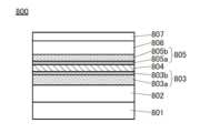
본 발명의 일 형태는 제 1 절연체 위의 제 1 도전체와, 제 1 도전체 위의 강유전체층과, 강유전체층 위의 제 2 도전체와, 제 2 도전체 위의 제 2 절연체와, 제 1 도전체, 강유전체층, 제 2 도전체, 및 제 2 절연체를 감싸는 제 3 절연체를 가지고, 제 2 절연체는 수소를 포획 또는 고착하는 기능을 가지고, 제 3 절연체는 수소의 확산을 억제하는 기능을 가지는 강유전체 디바이스이다. One aspect of the present invention is a first conductor over a first insulator, a ferroelectric layer over the first conductor, a second conductor over the ferroelectric layer, a second insulator over the second conductor, and A conductor, a ferroelectric layer, a second conductor, and a third insulator surrounding the second insulator, the second insulator has a function of trapping or fixing hydrogen, and the third insulator has a function of suppressing the diffusion of hydrogen. It is a ferroelectric device.
상기에 있어서, 제 2 절연체는 산소와 알루미늄을 가지고, 제 3 절연체는 질소와 실리콘을 가지는 것이 바람직하다. 또한 상기에 있어서, 제 2 절연체는 비정질 구조를 가지는 것이 바람직하다. 또한 상기에 있어서, 제 1 절연체는 질소와 실리콘을 가지는 것이 바람직하다. In the above, it is preferable that the second insulator contains oxygen and aluminum, and the third insulator contains nitrogen and silicon. In addition, in the above, it is preferable that the second insulator has an amorphous structure. Further, in the above, it is preferable that the first insulator contains nitrogen and silicon.
상기에 있어서, 강유전체층은 하프늄과 지르코늄을 가지는 것이 바람직하다. 또한 상기에 있어서, 강유전체층에 포함되는 수소의 농도는 SIMS 분석에서 5×10²⁰atoms/cm3 이하인 것이 바람직하다.In the above, the ferroelectric layer preferably contains hafnium and zirconium. In addition, in the above, the concentration of hydrogen contained in the ferroelectric layer is preferably 5×10 20 atoms/cm 3 or less in SIMS analysis.
또한 본 발명의 다른 일 형태는 상기 강유전체 디바이스와, 트랜지스터를 가지고, 트랜지스터는 제 1 절연체 아래에 배치되고, 트랜지스터는 채널 형성 영역에 산화물 반도체를 가지는 반도체 장치이다. 또한 상기에 있어서, 트랜지스터의 소스 및 드레인 중 한쪽은 제 1 도전체와 전기적으로 접속되는 것이 바람직하다. Another aspect of the present invention is a semiconductor device including the above ferroelectric device and a transistor, the transistor disposed under the first insulator, and the transistor including an oxide semiconductor in a channel formation region. Further, in the above, it is preferable that one of the source and drain of the transistor is electrically connected to the first conductor.
또는 본 발명의 일 형태에 의하여 강유전성을 가질 수 있는 재료를 이용한 용량 소자를 제공할 수 있다. 또는 본 발명의 일 형태에 의하여 강유전성을 가질 수 있는 재료를 이용한 트랜지스터를 제공할 수 있다. 또는 본 발명의 일 형태에 의하여 강유전성을 가질 수 있는 재료를 이용한 용량 소자 및 다이오드를 제공할 수 있다. 또는 본 발명의 일 형태에 의하여 강유전성을 가질 수 있는 재료를 이용하고, 또한 터널 접합을 이용한 소자를 제공할 수 있다. Alternatively, according to one embodiment of the present invention, a capacitance element using a material capable of ferroelectricity can be provided. Alternatively, according to one embodiment of the present invention, a transistor using a material capable of having ferroelectricity can be provided. Alternatively, according to one embodiment of the present invention, a capacitance element and a diode using a material having ferroelectricity may be provided. Alternatively, one embodiment of the present invention can provide a device using a material capable of ferroelectricity and using a tunnel junction.
또한 이들 효과의 기재는 다른 효과의 존재를 방해하는 것은 아니다. 또한 본 발명의 일 형태는 이들 효과 모두를 가질 필요는 없다. 또한 이들 외의 효과는 명세서, 도면, 청구항 등의 기재로부터 저절로 명백해지는 것이며 명세서, 도면, 청구항 등의 기재에서 이들 외의 효과가 추출될 수 있다. In addition, the description of these effects does not prevent the existence of other effects. Also, one embodiment of the present invention need not have all of these effects. In addition, effects other than these are self-evident from the description of the specification, drawings, claims, etc., and effects other than these can be extracted from the description of the specification, drawings, claims, etc.
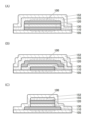
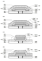
도 1의 (A) 내지 (C)는 본 발명의 일 형태인 용량 소자의 단면도이다.
도 2는 본 발명의 일 형태에 따른 산화 하프늄의 결정 구조를 설명하는 모델도이다.
도 3의 (A) 내지 (C)는 본 발명의 일 형태인 HfZrOx의 결정 구조의 모델도이다. 도 3의 (D)는 강유전체층의 히스테리시스 특성의 일례를 나타내는 그래프이다.
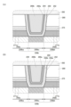
도 4의 (A) 내지 (C)는 용량 소자가 가지는 강유전체의 모식도이다.
도 5의 (A1), (B1), 및 (C1)은 본 발명의 일 형태에 따른 반도체 장치의 회로도를 설명하는 도면이다. 도 5의 (A2), (B2), (C2), (C3), 및 (C4)는 본 발명의 일 형태에 따른 반도체 장치의 단면 구조를 설명하는 도면이다.
도 6의 (A) 내지 (C)는 본 발명의 일 형태인 용량 소자의 제작 방법을 나타낸 단면도이다.
도 7의 (A)는 본 발명의 일 형태에 따른 금속 산화물막의 성막 시퀀스를 나타낸 도면이다. 도 7의 (B)는 본 발명의 일 형태에 따른 금속 산화물막의 제조 장치의 단면도이다. 도 7의 (C)는 산화물의 성막 시퀀스를 나타낸 도면이다.
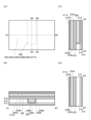
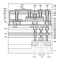
도 8의 (A)는 본 발명의 일 형태인 반도체 장치의 상면도이다. 도 8의 (B) 내지 (D)는 본 발명의 일 형태인 반도체 장치의 단면도이다.
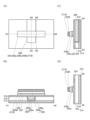
도 9의 (A) 및 (B)는 본 발명의 일 형태인 반도체 장치의 단면도이다.
도 10의 (A)는 IGZO의 결정 구조의 분류를 설명하는 도면이다. 도 10의 (B)는 CAAC-IGZO막의 XRD 스펙트럼을 설명하는 도면이다. 도 10의 (C)는 CAAC-IGZO막의 나노빔 전자 회절 패턴을 설명하는 도면이다.
도 11의 (A)는 본 발명의 일 형태에 따른 반도체 장치의 평면도이다. 도 11의 (B) 및 (C)는 본 발명의 일 형태인 반도체 장치의 단면도이다.
도 12의 (A)는 본 발명의 일 형태인 반도체 장치의 제작 방법을 나타낸 상면도이다. 도 12의 (B) 내지 (D)는 본 발명의 일 형태인 반도체 장치의 제작 방법을 나타낸 단면도이다.
도 13의 (A)는 본 발명의 일 형태인 반도체 장치의 제작 방법을 나타낸 상면도이다. 도 13의 (B) 내지 (D)는 본 발명의 일 형태인 반도체 장치의 제작 방법을 나타낸 단면도이다.
도 14의 (A)는 본 발명의 일 형태인 반도체 장치의 제작 방법을 나타낸 상면도이다. 도 14의 (B) 내지 (D)는 본 발명의 일 형태인 반도체 장치의 제작 방법을 나타낸 단면도이다.
도 15의 (A)는 본 발명의 일 형태인 반도체 장치의 제작 방법을 나타낸 상면도이다. 도 15의 (B) 내지 (D)는 본 발명의 일 형태인 반도체 장치의 제작 방법을 나타낸 단면도이다.
도 16의 (A)는 본 발명의 일 형태인 반도체 장치의 제작 방법을 나타낸 상면도이다. 도 16의 (B) 내지 (D)는 본 발명의 일 형태인 반도체 장치의 제작 방법을 나타낸 단면도이다.
도 17의 (A)는 본 발명의 일 형태인 반도체 장치의 제작 방법을 나타낸 상면도이다. 도 17의 (B) 내지 (D)는 본 발명의 일 형태인 반도체 장치의 제작 방법을 나타낸 단면도이다.
도 18의 (A) 및 (B)는 본 발명의 일 형태인 반도체 장치의 단면도이다.
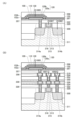
도 19의 (A) 내지 (D)는 본 발명의 일 형태인 용량 소자의 단면도이다.
도 20의 (A) 내지 (C)는 본 발명의 일 형태인 반도체 장치의 단면도이다.
도 21의 (A) 내지 (C)는 본 발명의 일 형태에 따른 소자의 구성을 나타낸 단면도이다.
도 22는 본 발명의 일 형태에 따른 기억 장치의 구성을 나타낸 단면도이다.
도 23은 본 발명의 일 형태에 따른 기억 장치의 구성을 나타낸 단면도이다.
도 24의 (A) 및 (B)는 본 발명의 일 형태에 따른 기억 장치의 구성을 나타낸 단면도이다.
도 25는 본 발명의 일 형태에 따른 기억 장치의 구성을 나타낸 단면도이다.
도 26은 본 발명의 일 형태에 따른 기억 장치의 구성을 나타낸 단면도이다.
도 27의 (A) 및 (B)는 본 발명의 일 형태에 따른 기억 장치의 구성을 나타낸 단면도이다.
도 28의 (A)는 본 발명의 일 형태에 따른 기억 장치의 구성예를 나타낸 블록도이다. 도 28의 (B)는 본 발명의 일 형태에 따른 기억 장치의 구성예를 나타낸 모식도이다.
도 29의 (A)는 메모리 셀의 구성예를 나타낸 회로도이다. 도 29의 (B1)은 강유전체층의 히스테리시스 특성의 일례를 나타내는 그래프이다. 도 29의 (B2)는 이상적인 강유전체층의 히스테리시스 특성의 일례를 나타내는 그래프이다. 도 29의 (C)는 메모리 셀의 구동 방법의 일례를 나타내는 타이밍 차트이다.
도 30의 (A) 내지 (E)는 본 발명의 일 형태에 따른 기억 장치의 모식도이다.
도 31의 (A) 내지 (H)는 본 발명의 일 형태에 따른 전자 기기를 나타낸 도면이다.
도 32는 시료의 단면 개략도이다.
도 33은 SIMS 분석 결과를 나타낸 도면이다.
도 34의 (A) 및 (B)는 SIMS 분석 결과를 나타낸 도면이다.
도 35는 SIMS 분석 결과를 나타낸 도면이다.
도 36의 (A) 및 (B)는 SIMS 분석 결과를 나타낸 도면이다.
도 37은 본 실시예에 따른 시료의 모식도이다.
도 38의 (A) 내지 (C)는 본 실시예에 따른 TEM 이미지이다.
도 39는 본 실시예에 따른 시료의 수소 농도를 나타낸 도면이다.
도 40의 (A) 및 (B)는 본 실시예에 따른 TE 이미지이다.
도 41의 (A) 및 (B)는 본 실시예에 따른 TE 이미지이다.
도 42의 (A) 및 (B)는 본 실시예에 따른 TE 이미지이다.1(A) to (C) are cross-sectional views of a capacitance element according to one embodiment of the present invention.
2 is a model diagram explaining the crystal structure of hafnium oxide according to one embodiment of the present invention.
3(A) to (C) are model diagrams of the crystal structure of HfZrO x as one embodiment of the present invention. 3(D) is a graph showing an example of the hysteresis characteristics of the ferroelectric layer.
4(A) to (C) are schematic diagrams of the ferroelectric of the capacitive element.
5 (A1), (B1), and (C1) are diagrams for explaining circuit diagrams of the semiconductor device according to one embodiment of the present invention. 5 (A2), (B2), (C2), (C3), and (C4) are diagrams for explaining a cross-sectional structure of a semiconductor device according to one embodiment of the present invention.
6(A) to (C) are cross-sectional views showing a manufacturing method of a capacitance element according to one embodiment of the present invention.
7(A) is a diagram showing a deposition sequence of a metal oxide film according to one embodiment of the present invention. Fig. 7(B) is a cross-sectional view of a metal oxide film manufacturing apparatus according to one embodiment of the present invention. 7(C) is a diagram showing an oxide film formation sequence.
8(A) is a top view of a semiconductor device according to one embodiment of the present invention. 8(B) to (D) are cross-sectional views of a semiconductor device according to one embodiment of the present invention.
9(A) and (B) are cross-sectional views of a semiconductor device according to one embodiment of the present invention.
Fig. 10 (A) is a diagram explaining the classification of the crystal structure of IGZO. Fig. 10(B) is a diagram explaining the XRD spectrum of the CAAC-IGZO film. FIG. 10(C) is a diagram explaining a nanobeam electron diffraction pattern of a CAAC-IGZO film.
11(A) is a plan view of a semiconductor device according to one embodiment of the present invention. 11(B) and (C) are cross-sectional views of a semiconductor device according to one embodiment of the present invention.
12(A) is a top view showing a manufacturing method of a semiconductor device according to one embodiment of the present invention. 12(B) to (D) are cross-sectional views showing a method of manufacturing a semiconductor device according to one embodiment of the present invention.
13(A) is a top view showing a manufacturing method of a semiconductor device according to one embodiment of the present invention. 13(B) to (D) are cross-sectional views showing a method of manufacturing a semiconductor device according to one embodiment of the present invention.
Fig. 14(A) is a top view showing a manufacturing method of a semiconductor device according to one embodiment of the present invention. 14(B) to (D) are cross-sectional views showing a method of manufacturing a semiconductor device according to one embodiment of the present invention.
15(A) is a top view showing a manufacturing method of a semiconductor device according to one embodiment of the present invention. 15(B) to (D) are cross-sectional views showing a method of manufacturing a semiconductor device according to one embodiment of the present invention.
16(A) is a top view showing a method of manufacturing a semiconductor device according to one embodiment of the present invention. 16(B) to (D) are cross-sectional views showing a method of manufacturing a semiconductor device according to one embodiment of the present invention.
17(A) is a top view showing a method of manufacturing a semiconductor device according to one embodiment of the present invention. 17(B) to (D) are cross-sectional views illustrating a method of manufacturing a semiconductor device according to one embodiment of the present invention.
18(A) and (B) are cross-sectional views of a semiconductor device according to one embodiment of the present invention.
19(A) to (D) are cross-sectional views of a capacitance element according to one embodiment of the present invention.
20(A) to (C) are cross-sectional views of a semiconductor device according to one embodiment of the present invention.
21(A) to (C) are cross-sectional views showing the configuration of an element according to one embodiment of the present invention.
22 is a cross-sectional view showing the configuration of a storage device according to one embodiment of the present invention.
23 is a cross-sectional view showing the configuration of a storage device according to one embodiment of the present invention.
24(A) and (B) are sectional views showing the configuration of a storage device according to one embodiment of the present invention.
25 is a cross-sectional view showing the configuration of a storage device according to one embodiment of the present invention. 26 is a cross-sectional view showing the configuration of a storage device according to one embodiment of the present invention.
27(A) and (B) are sectional views showing the configuration of a storage device according to one embodiment of the present invention.
Fig. 28(A) is a block diagram showing a configuration example of a storage device according to one embodiment of the present invention. Fig. 28(B) is a schematic diagram showing a configuration example of a storage device according to one embodiment of the present invention.
29(A) is a circuit diagram showing a configuration example of a memory cell. 29(B1) is a graph showing an example of the hysteresis characteristics of the ferroelectric layer. 29(B2) is a graph showing an example of hysteresis characteristics of an ideal ferroelectric layer. 29(C) is a timing chart showing an example of a method of driving a memory cell.
30(A) to (E) are schematic diagrams of a storage device according to one embodiment of the present invention.
31(A) to (H) are diagrams showing an electronic device according to one embodiment of the present invention.
32 is a schematic cross-sectional view of a sample.
33 is a diagram showing the results of SIMS analysis.
34 (A) and (B) are diagrams showing the results of SIMS analysis.
35 is a diagram showing the results of SIMS analysis.
36 (A) and (B) are views showing the results of SIMS analysis.
37 is a schematic diagram of a sample according to this embodiment.
38 (A) to (C) are TEM images according to the present embodiment.
39 is a diagram showing the hydrogen concentration of a sample according to the present embodiment.
40 (A) and (B) are TE images according to the present embodiment.
41 (A) and (B) are TE images according to the present embodiment.
42 (A) and (B) are TE images according to the present embodiment.
이하에서, 실시형태에 대하여 도면을 참조하여 설명한다. 다만 실시형태는 많은 상이한 형태로 실시할 수 있고, 취지 및 그 범위에서 벗어남이 없이 그 형태 및 자세한 사항을 다양하게 변경할 수 있다는 것은 통상의 기술자라면 용이하게 이해할 수 있다. 따라서 본 발명은 이하의 실시형태의 기재 내용에 한정하여 해석되는 것이 아니다. EMBODIMENT OF THE INVENTION Below, embodiment is described with reference to drawings. However, those skilled in the art can easily understand that the embodiment can be implemented in many different forms, and that the form and details can be changed in various ways without departing from the spirit and scope thereof. Therefore, the present invention is not construed as being limited to the description of the following embodiments.
또한 도면에서 크기, 층의 두께, 또는 영역은 명료화를 위하여 과장되어 있는 경우가 있다. 따라서 반드시 그 스케일에 한정되는 것은 아니다. 또한 도면은 이상적인 예를 모식적으로 나타낸 것이고, 도면에 나타낸 형상 또는 값 등에 한정되지 않는다. 예를 들어 실제의 제조 공정에서, 에칭 등의 처리에 의하여 층, 레지스트 마스크 등이 의도하지 않게 감소되는 경우가 있지만, 이해를 용이하게 하기 위하여 도면에 반영하지 않는 경우가 있다. 또한 도면에서 동일한 부분 또는 같은 기능을 가지는 부분에는 동일한 부호를 상이한 도면 사이에서 공통적으로 사용하고, 이에 대한 반복적인 설명은 생략하는 경우가 있다. 또한 같은 기능을 가지는 부분을 가리키는 경우에는 해치 패턴을 동일하게 하고, 특별히 부호를 붙이지 않는 경우가 있다. Also, in the drawings, the size, layer thickness, or area may be exaggerated for clarity. Therefore, it is not necessarily limited to that scale. In addition, the drawing schematically shows an ideal example, and is not limited to the shape or value shown in the drawing. For example, in actual manufacturing processes, layers, resist masks, and the like may be unintentionally reduced by processing such as etching, but may not be reflected in drawings for ease of understanding. In addition, the same reference numerals are commonly used in different drawings for the same parts or parts having the same functions in the drawings, and a repetitive explanation thereof may be omitted. In addition, in the case of indicating parts having the same function, the same hatch pattern is used, and there are cases where no special code is attached.
또한 특히 상면도('평면도'라고도 함), 사시도 등에서, 발명의 이해를 용이하게 하기 위하여 일부의 구성 요소의 기재를 생략하는 경우가 있다. 또한 일부의 숨은선 등의 기재를 생략하는 경우가 있다. In particular, description of some components may be omitted in order to facilitate understanding of the invention, especially in a top view (also referred to as a 'plan view'), a perspective view, or the like. In addition, descriptions of some hidden lines and the like may be omitted.
또한 본 명세서 등에서 제 1, 제 2 등으로 붙여지는 서수사는 편의상 사용되는 것이며, 공정 순서 또는 적층 순서를 나타내는 것이 아니다. 그러므로 예를 들어 '제 1'을 '제 2' 또는 '제 3' 등으로 적절히 바꿔 설명할 수 있다. 또한 본 명세서 등에 기재되는 서수사와, 본 발명의 일 형태를 특정하기 위하여 사용되는 서수사는 일치하지 않는 경우가 있다. In addition, in this specification and the like, the ordinal numerals attached to first, second, etc. are used for convenience, and do not indicate a process order or stacking order. Therefore, for example, 'first' may be appropriately replaced with 'second' or 'third'. In addition, there are cases in which the ordinal numbers described in this specification and the like do not coincide with the ordinal numbers used to specify one embodiment of the present invention.
또한 본 명세서 등에서 '위에', '아래에' 등의 배치를 나타내는 어구는 구성끼리의 위치 관계를 도면을 참조하여 설명하기 위하여 편의상 사용하고 있다. 또한 구성끼리의 위치 관계는 각 구성을 묘사하는 방향에 따라 적절히 변화된다. 따라서 명세서에서 설명된 어구에 한정되지 않고, 상황에 따라 적절히 바꿔 말할 수 있다. Also, in this specification and the like, phrases indicating arrangement such as 'above' and 'below' are used for convenience to describe the positional relationship between components with reference to the drawings. In addition, the positional relationship between the components changes appropriately according to the direction in which each component is described. Therefore, it is not limited to the phrases described in the specification, and may be appropriately changed depending on the situation.
예를 들어 본 명세서 등에서 X와 Y가 접속된다고 명시적으로 기재되는 경우에는, X와 Y가 전기적으로 접속되는 경우와, X와 Y가 기능적으로 접속되는 경우와, X와 Y가 직접적으로 접속되는 경우가 본 명세서 등에 개시되어 있는 것으로 한다. 따라서 소정의 접속 관계, 예를 들어 도면 또는 문장에 나타낸 접속 관계에 한정되지 않고, 도면 또는 문장에 나타낸 접속 관계 이외의 것도 도면 또는 문장에 개시되어 있는 것으로 한다. 여기서 X, Y는 대상물(예를 들어 장치, 소자, 회로, 배선, 전극, 단자, 도전막, 층 등)인 것으로 한다. For example, when it is explicitly stated that X and Y are connected in this specification and the like, when X and Y are electrically connected, when X and Y are functionally connected, and when X and Y are directly connected It is assumed that the case is disclosed in this specification and the like. Therefore, it is assumed that the connection relationship other than the connection relationship shown in the drawing or text is also disclosed in the drawing or text, without being limited to the predetermined connection relationship, for example, the connection relationship shown in the drawing or text. Here, X and Y are assumed to be objects (for example, devices, elements, circuits, wires, electrodes, terminals, conductive films, layers, etc.).
또한 본 명세서 등에서 트랜지스터란, 게이트와, 드레인과, 소스를 포함하는 적어도 3개의 단자를 가지는 소자이다. 그리고 드레인(드레인 단자, 드레인 영역, 또는 드레인 전극)과 소스(소스 단자, 소스 영역, 또는 소스 전극) 사이에 채널이 형성되는 영역(이하 채널 형성 영역이라고도 함)을 가지고, 채널 형성 영역을 통하여 소스와 드레인 사이에 전류를 흘릴 수 있다. 또한 본 명세서 등에서 채널 형성 영역이란, 전류가 주로 흐르는 영역을 말한다. In this specification and the like, a transistor is an element having at least three terminals including a gate, a drain, and a source. and a region (hereinafter referred to as a channel forming region) in which a channel is formed between the drain (drain terminal, drain region, or drain electrode) and the source (source terminal, source region, or source electrode), and the source through the channel forming region. A current can flow between the and the drain. Also, in this specification and the like, a channel formation region refers to a region through which current mainly flows.
또한 소스 또는 드레인의 기능은 상이한 극성의 트랜지스터를 채용하는 경우, 또는 회로 동작에서 전류의 방향이 변화되는 경우 등에는 서로 바뀌는 경우가 있다. 그러므로 본 명세서 등에서는 소스와 드레인이라는 용어는 서로 바꿔 사용할 수 있는 경우가 있다. In addition, the function of the source or drain may be reversed when transistors of different polarities are employed, or when the direction of current is changed in circuit operation. Therefore, in this specification and the like, the terms source and drain may be used interchangeably.
또한 채널 길이란, 예를 들어 트랜지스터의 상면도에서, 반도체(또는 트랜지스터가 온 상태일 때 반도체 중에서 전류가 흐르는 부분)와 게이트 전극이 서로 중첩되는 영역, 또는 채널 형성 영역에서의 소스(소스 영역 또는 소스 전극)와 드레인(드레인 영역 또는 드레인 전극) 사이의 거리를 말한다. 또한 하나의 트랜지스터에서, 채널 길이가 모든 영역에서 같은 값을 취한다고 할 수는 없다. 즉 하나의 트랜지스터의 채널 길이는 하나의 값으로 정해지지 않는 경우가 있다. 따라서 본 명세서에서 채널 길이는 채널 형성 영역에서의 어느 하나의 값, 최댓값, 최솟값, 또는 평균값으로 한다. In addition, the channel length means, for example, in a top view of a transistor, a region where a semiconductor (or a portion of a semiconductor where current flows when the transistor is in an on state) and a gate electrode overlap each other, or a source in a channel formation region (source region or It refers to the distance between the source electrode) and the drain (drain region or drain electrode). Also, in one transistor, it cannot be said that the channel length takes the same value in all regions. That is, there are cases in which the channel length of one transistor is not determined by one value. Therefore, in this specification, the channel length is any one value, maximum value, minimum value, or average value in the channel formation region.
채널 폭이란, 예를 들어 트랜지스터의 상면도에서, 반도체(또는 트랜지스터가 온 상태일 때 반도체 중에서 전류가 흐르는 부분)와 게이트 전극이 서로 중첩되는 영역, 또는 채널 형성 영역에서의 채널 길이 방향에 수직인 방향의 채널 형성 영역의 길이를 말한다. 또한 하나의 트랜지스터에서, 채널 폭이 모든 영역에서 같은 값을 취한다고 할 수는 없다. 즉 하나의 트랜지스터의 채널 폭은 하나의 값으로 정해지지 않는 경우가 있다. 따라서 본 명세서에서 채널 폭은 채널 형성 영역에서의 어느 하나의 값, 최댓값, 최솟값, 또는 평균값으로 한다. The channel width is, for example, in a top view of a transistor, a region where a semiconductor (or a portion of a semiconductor where current flows when the transistor is in an on state) and a gate electrode overlap each other, or a channel width perpendicular to the channel length direction in a channel formation region. It refers to the length of the channel formation region in the direction. Also, in one transistor, it cannot be said that the channel width takes the same value in all regions. That is, there are cases in which the channel width of one transistor is not determined by one value. Therefore, in this specification, the channel width is any one value, maximum value, minimum value, or average value in the channel formation region.
또한 본 명세서 등에서 트랜지스터의 구조에 따라서는, 실제로 채널이 형성되는 영역에서의 채널 폭(이하 '실효적인 채널 폭'이라고도 함)과 트랜지스터의 상면도에 나타내는 채널 폭(이하 '외관상 채널 폭'이라고도 함)이 상이한 경우가 있다. 예를 들어 게이트 전극이 반도체의 측면을 덮는 경우, 실효적인 채널 폭이 외관상 채널 폭보다 커져, 그 영향을 무시할 수 없는 경우가 있다. 예를 들어 미세하고 게이트 전극이 반도체의 측면을 덮는 트랜지스터에서는, 반도체의 측면에 형성되는 채널 형성 영역의 비율이 높아지는 경우가 있다. 이 경우에는 외관상 채널 폭보다 실효적인 채널 폭이 더 크다. In this specification and the like, depending on the structure of the transistor, the channel width in the region where the channel is actually formed (hereinafter also referred to as 'effective channel width') and the channel width shown in the top view of the transistor (hereinafter also referred to as 'external channel width') ) may be different. For example, when the gate electrode covers the side surface of the semiconductor, the effective channel width apparently becomes larger than the channel width, and the effect may not be ignored. For example, in a thin transistor in which the gate electrode covers the side surface of the semiconductor, the ratio of the channel formation region formed on the side surface of the semiconductor may increase. In this case, the effective channel width is larger than the apparent channel width.
이러한 경우, 실효적인 채널 폭을 실측에 의하여 추정하기 어려운 경우가 있다. 예를 들어 설곗값으로부터 실효적인 채널 폭을 추정하기 위해서는, 반도체의 형상을 미리 알고 있다는 가정이 필요하다. 따라서 반도체의 형상을 정확하게 알 수 없는 경우에는 실효적인 채널 폭을 정확하게 측정하기 어렵다. In this case, it may be difficult to estimate the effective channel width by actual measurement. For example, in order to estimate an effective channel width from a design value, it is necessary to assume that the shape of a semiconductor is known in advance. Therefore, when the shape of the semiconductor is not accurately known, it is difficult to accurately measure an effective channel width.
본 명세서에서 단순히 채널 폭이라고 기재한 경우에는 외관상 채널 폭을 가리키는 경우가 있다. 또는 본 명세서에서 단순히 채널 폭이라고 기재한 경우에는 실효적인 채널 폭을 가리키는 경우가 있다. 또한 채널 길이, 채널 폭, 실효적인 채널 폭, 외관상 채널 폭 등은 단면 TEM 이미지 등을 해석하는 것 등에 의하여 값을 결정할 수 있다. In this specification, when simply described as a channel width, it may refer to a channel width in appearance. Alternatively, in the present specification, when simply described as a channel width, it may indicate an effective channel width. In addition, the channel length, channel width, effective channel width, apparent channel width, etc. can be determined by analyzing a cross-sectional TEM image or the like.
또한 반도체의 불순물이란, 예를 들어 반도체를 구성하는 주성분 외의 것을 말한다. 예를 들어 농도가 0.1atomic% 미만인 원소는 불순물이라고 할 수 있다. 불순물이 포함됨으로써, 예를 들어 반도체의 결함 준위 밀도가 높아지거나, 결정성이 저하되는 경우가 있다. 반도체가 산화물 반도체인 경우, 반도체의 특성을 변화시키는 불순물로서는, 예를 들어 1족 원소, 2족 원소, 13족 원소, 14족 원소, 15족 원소, 산화물 반도체의 주성분 외의 전이 금속(transition metal) 등이 있고, 예를 들어 수소, 리튬, 소듐, 실리콘, 붕소, 인, 탄소, 질소 등이 있다. 또한 물도 불순물로서 기능하는 경우가 있다. 또한 예를 들어 불순물의 혼입으로 인하여 산화물 반도체에 산소 결손(VO: oxygen vacancy라고도 함)이 형성되는 경우가 있다.In addition, the impurity of a semiconductor means things other than the main component which comprises a semiconductor, for example. For example, an element with a concentration less than 0.1 atomic % can be considered an impurity. When impurities are contained, the density of defect states of the semiconductor may increase or the crystallinity may decrease, for example. When the semiconductor is an oxide semiconductor, the impurity that changes the characteristics of the semiconductor is, for example, a
또한 본 명세서 등에서 산화질화물이란, 그 조성으로서 질소보다 산소의 함유량이 많은 것을 가리킨다. 예를 들어 산화질화 실리콘은 그 조성으로서 질소보다 산소의 함유량이 많다. 또한 질화 산화물이란, 그 조성으로서 산소보다 질소의 함유량이 많은 것을 가리킨다. 예를 들어 질화산화 실리콘은 그 조성으로서 산소보다 질소의 함유량이 많다. In this specification and the like, an oxynitride refers to a material having a higher content of oxygen than nitrogen as its composition. For example, silicon oxynitride contains more oxygen than nitrogen as its composition. In addition, a nitride oxide refers to the thing with more nitrogen content than oxygen as its composition. For example, silicon nitride oxide contains more nitrogen than oxygen as its composition.
또한 본 명세서 등에서 '절연체'라는 용어를 절연막 또는 절연층으로 바꿔 말할 수 있다. 또한 '도전체'라는 용어를 도전막 또는 도전층으로 바꿔 말할 수 있다. 또한 '반도체'라는 용어를 반도체막 또는 반도체층으로 바꿔 말할 수 있다. Also, in this specification and the like, the term 'insulator' may be referred to as an insulating film or an insulating layer. Also, the term 'conductor' may be replaced with a conductive film or a conductive layer. Also, the term 'semiconductor' may be replaced with a semiconductor film or a semiconductor layer.
또한 본 명세서 등에서 '평행'이란, 2개의 직선이 -10° 이상 10° 이하의 각도로 배치되어 있는 상태를 말한다. 따라서 -5° 이상 5° 이하의 경우도 포함된다. 또한 '실질적으로 평행'이란, 2개의 직선이 -30° 이상 30° 이하의 각도로 배치되어 있는 상태를 말한다. 또한 '수직'이란, 2개의 직선이 80° 이상 100° 이하의 각도로 배치되어 있는 상태를 말한다. 따라서 85° 이상 95° 이하의 경우도 포함된다. 또한 '실질적으로 수직'이란, 2개의 직선이 60° 이상 120° 이하의 각도로 배치되어 있는 상태를 말한다. In this specification and the like, "parallel" refers to a state in which two straight lines are arranged at an angle of -10° or more and 10° or less. Therefore, the case of -5° or more and 5° or less is included. Also, 'substantially parallel' refers to a state in which two straight lines are arranged at an angle of -30° or more and 30° or less. Also, 'perpendicular' refers to a state in which two straight lines are arranged at an angle of 80° or more and 100° or less. Therefore, cases of 85° or more and 95° or less are included. Also, 'substantially vertical' refers to a state in which two straight lines are arranged at an angle of 60° or more and 120° or less.
본 명세서 등에서 금속 산화물(metal oxide)이란, 넓은 의미로의 금속의 산화물이다. 금속 산화물은 산화물 절연체, 산화물 도전체(투명 산화물 도전체를 포함함), 산화물 반도체(Oxide Semiconductor 또는 단순히 OS라고도 함) 등으로 분류된다. 예를 들어 트랜지스터의 반도체층에 금속 산화물을 사용한 경우, 상기 금속 산화물을 산화물 반도체라고 하는 경우가 있다. 즉 OS 트랜지스터라고 기재하는 경우에는, 금속 산화물 또는 산화물 반도체를 가지는 트랜지스터로 바꿔 말할 수 있다. In this specification and the like, a metal oxide is a metal oxide in a broad sense. Metal oxides are classified into oxide insulators, oxide conductors (including transparent oxide conductors), oxide semiconductors (also referred to as oxide semiconductors or simply OSs), and the like. For example, when a metal oxide is used for a semiconductor layer of a transistor, the metal oxide may be referred to as an oxide semiconductor. That is, when described as an OS transistor, it can be rephrased as a transistor having a metal oxide or an oxide semiconductor.
또한 본 명세서 등에서 노멀리 오프란, 게이트에 전위를 인가하지 않거나 또는 게이트에 접지 전위를 인가하였을 때, 트랜지스터를 흐르는 채널 폭 1μm당 드레인 전류가 실온에서 1×10-20A 이하, 85℃에서 1×10-18A 이하, 또는 125℃에서 1×10-16A 이하인 것을 말한다.In addition, in this specification and the like, when a potential is not applied to the gate, or when a ground potential is applied to the gate, the drain current per 1 μm of channel width flowing through the transistor is 1 × 10 -20 A or less at room temperature and 1 at 85 ° C. 10 -18 A or less, or 1x10 -16 A or less at 125 ° C.
또한 본 명세서에서 배리어 절연막이란, 배리어성을 가지는 절연막을 가리킨다. 본 명세서에서 배리어성이란, 대응하는 물질의 확산을 억제하는 기능(투과성이 낮다고도 함)을 말한다. 또는 대응하는 물질을 포획 또는 고착하는(게터링이라고도 함) 기능을 말한다. In this specification, a barrier insulating film refers to an insulating film having barrier properties. In this specification, barrier property refers to a function of suppressing diffusion of a corresponding substance (also referred to as low permeability). Alternatively, it refers to a function of trapping or fixing (also called gettering) a corresponding substance.
또한 본 명세서 등에서, "A가 B를 덮는다", "A가 B를 감싼다", 또는 "A가 B를 감싸 덮는다" 등의 기재는 B의 전체가 A에 의하여 가려져 있는 상태를 반드시 뜻하는 것이 아니다. "A가 B를 덮는다", "A가 B를 감싼다", 또는 "A가 B를 감싸 덮는다" 등의 기재는 B의 일부가 A에서 노출된 상태도 포함하는 것으로 한다. 또한 본 명세서 등에서, "A가 B를 덮는다"라는 기재를 "A가 B를 감싼다" 또는 "A가 B를 감싸 덮는다"로 바꿔 말할 수 있다. Also, in this specification and the like, descriptions such as "A covers B", "A covers B", or "A covers B" do not necessarily mean a state in which the entirety of B is covered by A. . Descriptions such as "A covers B", "A covers B", or "A covers B" include a state in which a part of B is exposed from A. In this specification and the like, the statement “A covers B” may be replaced with “A covers B” or “A covers B”.
(실시형태 1)(Embodiment 1)
본 실시형태에서는 도 1의 (A) 내지 도 7의 (B)를 사용하여 본 발명의 일 형태에 따른 용량 소자의 구성예에 대하여 설명한다. In this embodiment, an example of a configuration of a capacitance element according to one embodiment of the present invention will be described using FIGS. 1(A) to 7(B).
<용량 소자의 구성><Configuration of Capacitive Element>
도 1의 (A)에 나타낸 바와 같이, 본 발명의 일 형태에 따른 용량 소자(100)는 도전체(110)와, 도전체(120)와, 도전체(110)와 도전체(120) 사이에 끼워진 절연체(130)를 가진다. 예를 들어 절연체(105) 위에 도전체(110)가 배치되고, 도전체(110) 위에 절연체(130)가 배치되고, 절연체(130) 위에 도전체(120)가 배치되는 구성으로 하면 좋다. 여기서 도전체(110)는 용량 소자(100)의 하부 전극으로서 기능하고, 도전체(120)는 용량 소자(100)의 상부 전극으로서 기능하고, 절연체(130)는 용량 소자(100)의 유전체로서 기능한다.
As shown in FIG. 1(A) , in the
또한 도 1의 (A)에 나타낸 바와 같이, 용량 소자(100)를 감싸도록 절연체(152)가 배치되고, 적어도 절연체(152)와 절연체(130) 사이에 절연체(155)가 배치된다. 예를 들어 도 1의 (A)에 나타낸 바와 같이, 도전체(110), 절연체(130), 및 도전체(120)를 감싸도록 절연체(155)가 배치되고, 절연체(155)를 감싸도록 절연체(152)가 배치된다. 이때 절연체(155)가 도전체(110)와 중첩되지 않은 영역에서 절연체(105)와 접하여도 좋다.
As shown in FIG. 1(A), an
여기서, 절연체(152) 및 절연체(155)는 수소에 대한 배리어 절연막으로서 기능한다. 절연체(152)는 수소 및 수소가 결합된 물질(예를 들어 OH- 등) 중 적어도 하나의 확산을 억제하는 기능을 가진다. 따라서 절연체(152)는 수소 및 수소가 결합된 물질(예를 들어 OH- 등) 중 적어도 하나의 확산을 억제하는 능력이 절연체(130)보다 높은 것으로 한다. 또한 절연체(155)는 수소 및 수소가 결합된 물질 중 적어도 하나를 포획 또는 고착하는(게터링이라고도 함) 기능을 가진다. 따라서 절연체(155)는 수소 및 수소가 결합된 물질 중 적어도 하나를 포획 또는 고착하는 능력이 절연체(130)보다 높은 것으로 한다.Here, the
절연체(130)에는 강유전성을 가질 수 있는 재료를 사용하는 것이 바람직하다. 강유전성을 가질 수 있는 재료로서는 산화 하프늄, 산화 지르코늄, HfZrOx(X는 0보다 큰 실수로 함) 등의 금속 산화물을 들 수 있다. 또한 강유전성을 가질 수 있는 재료로서는 산화 하프늄에 원소 J1(여기서의 원소 J1은 지르코늄(Zr), 실리콘(Si), 알루미늄(Al), 가돌리늄(Gd), 이트륨(Y), 란타넘(La), 스트론튬(Sr) 등에서 선택된 하나 또는 복수임)을 첨가한 재료를 들 수 있다. 여기서 하프늄 원자와 원소 J1의 원자수의 비는 적절히 설정할 수 있고, 예를 들어 하프늄 원자와 원소 J1의 원자수를 1:1 또는 그 근방으로 하면 좋다. 또한 강유전성을 가질 수 있는 재료로서는 산화 지르코늄에 원소 J2(여기서의 원소 J2는 하프늄(Hf), 실리콘(Si), 알루미늄(Al), 가돌리늄(Gd), 이트륨(Y), 란타넘(La), 스트론튬(Sr) 등에서 선택된 하나 또는 복수임)를 첨가한 재료 등을 들 수 있다. 또한 지르코늄 원자와 원소 J2의 원자수의 비는 적절히 설정할 수 있고, 예를 들어 지르코늄 원자와 원소 J2의 원자수를 1:1 또는 그 근방으로 하면 좋다. 또한 강유전성을 가질 수 있는 재료로서, 타이타늄산 납(PbTiOx), 타이타늄산 바륨 스트론튬(BST), 타이타늄산 스트론튬, 타이타늄산 지르콘산 연(PZT), 탄탈럼산 비스무트산 스트론튬(SBT), 비스무트 페라이트(BFO), 타이타늄산 바륨 등의 페로브스카이트 구조를 가지는 압전성 세라믹을 사용하여도 좋다.It is preferable to use a material capable of ferroelectricity for the
또한 강유전성을 가질 수 있는 재료로서는 질화 알루미늄 스칸듐(Al1-aScaNb(a는 0보다 크고 0.5보다 작은 실수이고, b는 1 또는 그 근방의 값임)), Al-Ga-Sc 질화물, Ga-Sc 질화물 등의 금속 질화물을 들 수 있다. 또한 강유전성을 가질 수 있는 재료로서는 원소 M1과, 원소 M2와, 질소를 가지는 금속 질화물을 들 수 있다. 여기서 원소 M1은 알루미늄(Al), 갈륨(Ga), 인듐(In) 등에서 선택된 하나 또는 복수이다. 또한 원소 M2는 붕소(B), 스칸듐(Sc), 이트륨(Y), 란타넘(La), 세륨(Ce), 네오디뮴(Nd), 유로퓸(Eu), 타이타늄(Ti), 지르코늄(Zr), 하프늄(Hf), 바나듐(V), 나이오븀(Nb), 탄탈럼(Ta), 크로뮴(Cr) 등에서 선택된 하나 또는 복수이다. 또한 원소 M1의 원자수와 원소 M2의 원자수의 비는 적절히 설정할 수 있다. 또한 원소 M1과 질소를 가지는 금속 산화물은 원소 M2를 포함하지 않아도 강유전성을 가지는 경우가 있다. 또한 강유전성을 가질 수 있는 재료로서는 상기 금속 질화물에 원소 M3이 첨가된 재료를 들 수 있다. 또한 원소 M3은 마그네슘(Mg), 칼슘(Ca), 스트론튬(Sr), 아연(Zn), 카드뮴(Cd) 등에서 선택된 하나 또는 복수이다. 여기서 원소 M1의 원자수, 원소 M2의 원자수, 및 원소 M3의 원자수의 비는 적절히 설정할 수 있다. 또한 상기 금속 질화물은 적어도 13족 원소와, 15족 원소인 질소를 포함하기 때문에 상기 금속 질화물을 III-V족의 강유전체, III족 질화물의 강유전체 등이라고 부르는 경우가 있다.In addition, as a material capable of having ferroelectricity, aluminum scandium nitride (Al 1-a Sc a N b (a is a real number greater than 0 and less than 0.5, b is a value of 1 or near)), Al-Ga-Sc nitride, Metal nitrides, such as Ga-Sc nitride, are mentioned. Examples of materials capable of having ferroelectricity include metal nitrides having elements M1, M2, and nitrogen. Here, element M1 is one or more selected from aluminum (Al), gallium (Ga), indium (In), and the like. In addition, element M2 is boron (B), scandium (Sc), yttrium (Y), lanthanum (La), cerium (Ce), neodymium (Nd), europium (Eu), titanium (Ti), zirconium (Zr), It is one or more selected from hafnium (Hf), vanadium (V), niobium (Nb), tantalum (Ta), chromium (Cr), and the like. In addition, the ratio of the number of atoms of the element M1 to the number of atoms of the element M2 can be set appropriately. In addition, a metal oxide containing element M1 and nitrogen may have ferroelectricity even if element M2 is not included. Further, as a material capable of having ferroelectricity, a material in which element M3 is added to the above metal nitride is exemplified. In addition, element M3 is one or more selected from magnesium (Mg), calcium (Ca), strontium (Sr), zinc (Zn), cadmium (Cd), and the like. Here, the ratio of the number of atoms of the element M1, the number of atoms of the element M2, and the number of atoms of the element M3 can be set appropriately. In addition, since the metal nitride contains at least a group 13 element and nitrogen as a
또한 강유전성을 가질 수 있는 재료로서는 SrTaO2N, BaTaO2N 등의 페로브스카이트형 산질화물, κ알루미나형 구조의 GaFeO3 등을 들 수 있다.Examples of materials that can have ferroelectricity include perovskite-type oxynitrides such as SrTaO 2 N and BaTaO 2 N, GaFeO 3 having a κ-alumina structure, and the like.
또한 위의 설명에서는 금속 산화물 및 금속 질화물에 대하여 예시하였지만 이에 한정되지 않는다. 예를 들어 상술한 금속 산화물에 질소가 첨가된 금속 산화질화물 또는 상술한 금속 질화물에 산소가 첨가된 금속 질화산화물 등을 사용하여도 좋다. In addition, in the above description, metal oxide and metal nitride were exemplified, but are not limited thereto. For example, a metal oxynitride in which nitrogen is added to the above metal oxide or a metal nitride oxide in which oxygen is added to the above metal nitride may be used.
또한 강유전성을 가질 수 있는 재료로서는 예를 들어, 위에서 열거한 재료에서 선택된 복수의 재료로 이루어지는 혼합물 또는 화합물을 사용할 수 있다. 또는 절연체(130)를, 위에서 열거한 재료에서 선택된 복수의 재료로 이루어지는 적층 구조로 할 수 있다. 또한 위에서 열거한 재료 등은 성막 조건뿐만 아니라 각종 공정 등에 의해서도 결정 구조(특성)가 변화될 가능성이 있기 때문에, 본 명세서 등에서는 강유전성을 발현하는 재료를 강유전체라고만 부르는 것이 아니라 강유전성을 가질 수 있는 재료라고도 부른다. 또한 강유전체에는 강유전성을 발현하는 재료뿐만 아니라 강유전성을 가질 수 있는 재료도 포함되는 것으로 한다.
Also, as a material capable of having ferroelectricity, for example, a mixture or compound composed of a plurality of materials selected from the materials listed above can be used. Alternatively, the
그 중에서도, 강유전성을 가질 수 있는 재료로서, 산화 하프늄, 또는 산화 하프늄 및 산화 지르코늄을 가지는 재료는 수nm 등으로 얇은 막으로 가공하여도 강유전성을 가질 수 있기 때문에 바람직하다. 여기서 절연체(130)의 막 두께는 100nm 이하, 바람직하게는 50nm 이하, 더 바람직하게는 20nm 이하, 더욱 바람직하게는 10nm 이하(대표적으로는 2nm 이상 9nm 이하)로 할 수 있다. 예를 들어 막 두께를 8nm 이상 12nm 이하로 하는 것이 바람직하다. 박막화가 가능한 강유전체층으로 함으로써, 용량 소자(100)를 미세화된 트랜지스터 등의 반도체 소자에 조합하여 반도체 장치를 형성할 수 있다. 또한 본 명세서 등에 있어서, 강유전성을 가질 수 있는 재료를 층상으로 한 것을 강유전체층, 금속 산화물막, 또는 금속 질화물막이라고 부르는 경우가 있다. 또한 본 명세서 등에 있어서, 이러한 강유전체층, 금속 산화물막, 또는 금속 질화물막을 가지는 장치를 강유전체 디바이스라고 부르는 경우가 있다.
Among them, as a material capable of having ferroelectricity, hafnium oxide or a material having hafnium oxide and zirconium oxide is preferable because it can have ferroelectricity even when processed into a thin film of several nm or the like. Here, the film thickness of the
강유전성을 가질 수 있는 재료는 절연체이며, 외부로부터 전기장을 인가함으로써 내부에 분극이 발생하고, 또한 상기 전기장을 0으로 하여도 분극이 잔존하는 성질을 가진다. 그러므로 상기 재료를 유전체로서 사용한 용량 소자(이하 강유전 커패시터라고 부르는 경우가 있음)를 사용하여 비휘발성 기억 소자를 형성할 수 있다. 강유전 커패시터를 사용한 비휘발성 기억 소자는 FeRAM(Ferroelectric Random Access Memory), 강유전체 메모리 등이라고 불리는 경우가 있다. 예를 들어 강유전체 메모리는 트랜지스터와 강유전 커패시터를 가지고, 트랜지스터의 소스 및 드레인 중 한쪽이 강유전 커패시터의 한쪽 단자에 전기적으로 접속된 구성으로 할 수 있다. 따라서 본 실시형태에서 설명하는 용량 소자(100)와, 트랜지스터를 사용하는 반도체 장치는 강유전체 메모리로서 기능시킬 수 있다.
A material that can have ferroelectricity is an insulator, and has the property that polarization occurs inside when an electric field is applied from the outside, and polarization remains even when the electric field is set to zero. Therefore, a non-volatile memory element can be formed using a capacitive element (hereinafter sometimes referred to as a ferroelectric capacitor) using the above material as a dielectric. A non-volatile memory element using a ferroelectric capacitor is sometimes called FeRAM (Ferroelectric Random Access Memory), ferroelectric memory, or the like. For example, a ferroelectric memory may have a transistor and a ferroelectric capacitor, and one of the source and drain of the transistor is electrically connected to one terminal of the ferroelectric capacitor. Therefore, the semiconductor device using the
여기서, 절연체(130)에 사용할 수 있는 재료의 하나인 산화 하프늄의 결정 구조에 대하여 도 2를 사용하여 설명한다. 도 2는 산화 하프늄(본 실시형태에서는 HfO2)의 결정 구조를 설명하는 모델도이다. 산화 하프늄은 다양한 결정 구조를 취하는 것이 알려져 있으며, 예를 들어 도 2에 나타낸 입방정계(cubic, 공간군: Fm-3m), 정방정계(tetragonal, 공간군: P42/nmc), 직방정계(orthorhombic, 공간군: Pbc22), 및 단사정계(monoclinic, 공간군: P21/c) 등의 결정 구조를 취할 수 있다. 또한 도 2에 나타낸 바와 같이, 상술한 각 결정 구조는 상변화가 일어날 수 있다. 예를 들어 산화 하프늄에 지르코늄을 도핑한 복합 재료로 함으로써, 단사정계를 주로 한 산화 하프늄의 결정 구조에서 직방정계를 주로 한 결정 구조로 할 수 있다.Here, the crystal structure of hafnium oxide, which is one of the materials usable for the
상술한 복합 재료로서, ALD법 등을 사용하여 산화 하프늄과 산화 지르코늄을 대략 1:1의 조성이 되도록 번갈아 성막하는 경우, 상기 복합 재료는 직방정계 결정 구조를 가진다. 또는 상기 복합 재료는 비정질 구조를 가진다. 그 후에 상기 복합 재료에 열처리 등을 실시함으로써 비정질 구조를 직방정계 결정 구조로 할 수 있다. 또한 상기 직방정계 결정 구조는 단사정계 결정 구조로 변화되는 경우가 있다. 상술한 복합 재료에 강유전성을 부여하는 경우에는, 단사정계 결정 구조보다 직방정계 결정 구조가 바람직하다. As the composite material described above, when hafnium oxide and zirconium oxide are alternately formed in a composition of approximately 1:1 using an ALD method or the like, the composite material has a rectangular crystal structure. Alternatively, the composite material has an amorphous structure. Thereafter, by subjecting the composite material to heat treatment or the like, the amorphous structure can be converted into a rectangular crystal structure. In addition, there are cases where the above-described rectangular crystal structure changes to a monoclinic crystal structure. In the case of imparting ferroelectricity to the composite material described above, a rectangular crystal structure is preferable to a monoclinic crystal structure.
여기서, HfZrOx의 직방정계 결정 구조의 모델에 대하여 도 3의 (A)를 사용하여 설명한다.Here, the model of the rectangular crystal structure of HfZrO x is demonstrated using FIG. 3(A).
도 3의 (A)는 HfZrOx, 여기서는 Hf0.5Zr0.5O2의 결정 구조의 모델도이다. 또한 도 3의 (A) 중에서는 a축, b축, c축의 방향도 도시하였다. 도 3의 (A)에서는 HfO2의 orthorhombic 구조(Pca21)에 대하여 Zr를 층상으로 배치한 구조가 도시되어 있다. 또한 HfO2의 orthorhombic 구조의 셀은 제일원리 계산을 사용하여 구조 최적화를 수행하였다.3(A) is a model diagram of a crystal structure of HfZrO x , in this case, Hf 0.5 Zr 0.5 O 2 . Further, in FIG. 3(A), directions of the a-axis, b-axis, and c-axis are also shown. In (A) of FIG. 3, a structure in which Zr is arranged in a layered manner with respect to an orthorhombic structure (Pca2 1 ) of HfO 2 is shown. In addition, the orthorhombic cell of HfO 2 was structurally optimized using first-principle calculation.
또한 도 3의 (A)에서는 하프늄과 지르코늄이 산소를 통하여 서로 결합되어 있는 상태인 것을 알 수 있다. 이는 후술하는 성막 시퀀스와 같이, 하프늄과 지르코늄을 ALD법에 의하여 번갈아 성막함으로써 형성할 수 있다. In addition, in (A) of FIG. 3, it can be seen that hafnium and zirconium are bonded to each other through oxygen. This can be formed by alternately forming films of hafnium and zirconium by the ALD method, as in the film formation sequence described later.
외부로부터 전기장을 인가함으로써, 도 3의 (A) 중에 나타낸 산소의 일부가 변위되어, 내부에 분극이 발생한다. 여기서 산소의 일부는 c축 방향으로 변위되고, 분극도 c축 방향으로 발생한다. By applying an electric field from the outside, part of the oxygen shown in FIG. 3(A) is displaced, and polarization occurs inside. Here, some of the oxygen is displaced in the c-axis direction, and polarization also occurs in the c-axis direction.
도 3의 (B) 및 (C)는 HfZrOx, 여기서는 Hf0.5Zr0.5O2의 결정 구조의 모델도이다. 도 3의 (B) 및 (C)는 제일원리 계산에 의하여 원자의 배치가 최적화된 모델이다. 또한 도 3의 (A)에 나타낸 모델과 도 3의 (B)에 나타낸 모델은 원자의 표시 방법만이 다르고, 원자의 배치는 거의 같다.3 (B) and (C) are model diagrams of the crystal structure of HfZrO x , in this case Hf 0.5 Zr 0.5 O 2 . 3 (B) and (C) are models in which the arrangement of atoms is optimized by first-principle calculation. The model shown in Fig. 3(A) and the model shown in Fig. 3(B) differ only in the method of displaying atoms, and the arrangement of atoms is almost the same.
HfZrOx는 직방정계 결정 구조에서 도 3의 (B)에 나타낸 원자 배치 및 도 3의 (C)에 나타낸 원자 배치의 어느 쪽이든 취할 수 있다. 따라서 외부로부터 인가되는 전기장에 의하여 HfZrOx 중의 산소 원자의 일부가 변위됨으로써 내부에 분극이 발생한다. 또한 전기장의 방향 또는 강도를 바꿈으로써, HfZrOx 중의 산소 원자의 일부가 이동되어, 내부에 발생하는 분극의 부호가 변경된다.HfZrO x can take either of the atomic arrangement shown in FIG. 3(B) or the atomic arrangement shown in FIG. 3(C) in a rectangular crystal structure. Therefore, some of the oxygen atoms in HfZrO x are displaced by an electric field applied from the outside, thereby generating internal polarization. Also, by changing the direction or strength of the electric field, some of the oxygen atoms in HfZrO x are moved, and the sign of the polarization generated inside is changed.
도 3의 (D)는 강유전체층의 히스테리시스 특성의 일례를 나타내는 그래프이다. 도 3의 (D)에 있어서, 가로축은 강유전체층에 인가하는 전계 강도를 나타내고, 세로축은 강유전체층의 분극량을 나타낸다. 또한 도 3의 (D)에 나타낸 점(61)은 전계 강도가 0일 때의 최소 분극이고, 도 3의 (D)에 나타낸 점(62)은 전계 강도가 0일 때의 최대 분극이다. 예를 들어 최소 분극(도 3의 (D)에 나타낸 점(61))에서는 HfZrOx 중의 원자는 도 3의 (B)에 나타낸 바와 같은 배치를 취한다. 또한 최대 분극(도 3의 (D)에 나타낸 점(62))에서는 HfZrOx 중의 원자는 도 3의 (C)에 나타낸 바와 같은 배치를 취한다.3(D) is a graph showing an example of the hysteresis characteristics of the ferroelectric layer. In Fig. 3(D), the horizontal axis represents the intensity of the electric field applied to the ferroelectric layer, and the vertical axis represents the amount of polarization of the ferroelectric layer.
여기서, 도 1의 (A) 등에 나타낸, 강유전체층으로서 기능하는 절연체(130) 근방의 확대도를 도 4의 (A) 내지 (C)에 나타내었다.
Here, enlarged views of the vicinity of the
도 4의 (A)에 나타낸 바와 같이, 절연체(130)에서는 결정이 층을 형성하고, 상기 층이 적층된 결정 구조가 되어 있는 것이 바람직하다. 또한 상기 층은 도 3의 (A)에 나타낸 바와 같은 단결정 구조를 포함하는 것이 바람직하다. 또한 도 4의 (A)에 나타낸 절연체(130)의 파선은 결정의 층을 나타내고, 화살표(132)는 상기 결정의 c축을 나타낸다.
As shown in Fig. 4(A), it is preferable that the
절연체(130)에 포함되는 결정의 층은 a-b면 방향으로 신장되어 있다. 또한 절연체(130)에 포함되는 결정의 층은 c축 방향으로 성장되고(axial growth라고 불리는 경우가 있음), 복수의 결정의 층이 c축 방향으로 적층되어 있다. c축은 절연체(130)의 피형성면 또는 상면에 대략 수직인 방향을 향하는 것이 바람직하다. 예를 들어 도전체(110)의 상면에 대한 법선과 화살표(132)가 이루는 각도 θ가 30° 이하인 것이 바람직하고, 5° 이하인 것이 더 바람직하다.
The crystal layer included in the
또한 상기에서는 절연체(130)로서, 도 4의 (A) 등에 나타낸 바와 같은 단결정 구조를 가지는 강유전체층을 사용하는 예에 대하여 나타내었지만 본 발명은 이에 한정되지 않는다. 예를 들어 도 4의 (B)에 나타낸 바와 같이, 절연체(130)가 결정성이 다른 복수의 그레인(136)을 가지는 다결정 구조를 가져도 좋다. 여기서 복수의 그레인(136)의 적어도 일부는 직방정계 결정 구조를 가지는 것이 바람직하다. 복수의 그레인(136)의 적어도 일부에 직방정계 결정 구조를 가짐으로써 절연체(130)에 강유전성이 발현되기 때문에 바람직하다.
Further, in the foregoing, an example in which a ferroelectric layer having a single crystal structure as shown in FIG. For example, as shown in FIG. 4(B) , the
또한 절연체(130)가 단결정 구조를 가지는 층(138a)과 다결정의 층(138b)을 가지는 구성으로 하여도 좋다. 예를 들어 도 4의 (C)에 나타낸 바와 같이, 도전체(110) 위에 복수의 단결정 구조를 가지는 층(138a)과 복수의 다결정의 층(138b)이 적층된 구성으로 하여도 좋다.
Alternatively, the
절연체(130)의 결정 구조로서는 입방정계, 정방정계, 직방정계, 및 단사정계에서 선택되는 어느 하나 또는 복수로 하면 좋다. 특히 절연체(130)로서 직방정계 결정 구조를 가지면 강유전성이 발현되기 때문에 바람직하다. 또는 절연체(130)의 결정 구조는 비정질 구조를 가져도 좋다. 또는 절연체(130)는 비정질 구조와 결정 구조를 가지는 복합 구조를 가져도 좋다.
The crystal structure of the
또한 결정성이 양호한 절연체(130)를 형성하기 위해서는 절연체(130) 중의 수소, 탄소, 탄화수소, 또는 염소 등의 불순물이 저감되어 있는 것이 바람직하다. 여기서 상기 불순물은 단체(單體)의 원자만을 가리키는 것이 아니다. 절연체(130) 중에서 상술한 불순물 원소와 결합된 물질도 저감되어 있는 것이 바람직하다. 예를 들어 절연체(130) 중의 수소와 결합된 물질(예를 들어 OH- 등) 등도 저감되어 있는 것이 바람직하다. 이들 불순물은 절연체(130) 중의 결정에서 산소 결손을 형성하는 경우가 있다. 또한 상기 산소 결손 부분에 수소 등의 불순물 원소가 결합되어 절연체(130)의 결정성이 저하되는 경우가 있다. 따라서 이들 불순물이 절연체(130) 중에 포함됨으로써 절연체(130)의 결정화가 저해되는 경우가 있다. 상술한 바와 같이, 도 3의 (A)에 나타낸 결정 구조에 있어서, 외부 전기장에 의하여 산소가 변위됨으로써 강유전성이 발현한다. 따라서 절연체(130)의 강유전성을 향상시키기 위해서는 수소, 탄소, 탄화수소, 또는 염소 등의 불순물을 저감하는 것이 바람직하다.In addition, in order to form the
따라서 절연체(130)에는 수소, 탄소, 탄화수소, 또는 염소 등의 불순물을 포함하지 않거나, 이들의 함유량이 매우 적은 재료를 사용하는 것이 적합하다. 예를 들어 절연체(130)에 포함되는 수소의 농도는 5×10²⁰atoms/cm3 이하가 바람직하고, 1×10²⁰atoms/cm3 이하가 더 바람직하다. 또한 예를 들어 절연체(130)에 포함되는 탄소의 농도는 5×10²⁰atoms/cm3 이하가 바람직하고, 1×10²⁰atoms/cm3 이하가 더 바람직하고, 5×10¹⁹atoms/cm3 이하가 더욱 바람직하다. 또한 예를 들어 절연체(130)에 포함되는 염소의 농도는 5×10²¹atoms/cm3 이하가 바람직하고, 1×10²¹atoms/cm3 이하가 더 바람직하고, 5×10²⁰atoms/cm3 이하가 더욱 바람직하다. 또한 예를 들어 절연체(130)에 포함되는 탄화수소를 구성하는 탄소의 농도는 5×10²⁰atoms/cm3 이하가 바람직하고, 1×10²⁰atoms/cm3 이하가 더 바람직하고, 5×10¹⁹atoms/cm3 이하가 더욱 바람직하다.Therefore, it is appropriate to use a material that does not contain impurities such as hydrogen, carbon, hydrocarbons, or chlorine, or has a very low content thereof, for the
또한 상기 불순물의 정량은 이차 이온 질량 분석법(SIMS: Secondary Ion Mass Spectrometry), X선 광전자 분광법(XPS: X-ray Photoelectron Spectroscopy), 또는 오제 전자 분광법(AES: Auger Electron Spectroscopy)을 사용하여 수행할 수 있다. 예를 들어 SIMS 분석을 사용하여 절연체(130) 중의 수소, 탄소, 탄화수소, 또는 염소 등의 불순물을 정량하면 좋다.
In addition, the quantification of the impurities can be performed using secondary ion mass spectrometry (SIMS), X-ray photoelectron spectroscopy (XPS), or Auger electron spectroscopy (AES). there is. For example, impurities such as hydrogen, carbon, hydrocarbons, or chlorine in the
그래서 본 발명의 일 형태에서는 용량 소자(100)를 감싸도록 절연체(152)를 제공하고, 적어도 절연체(152)와 절연체(130) 사이에 절연체(155)를 제공하는 구성으로 한다. 절연체(152)에 의하여, 절연체(152) 외측으로부터 절연체(130)로 수소 등의 불순물이 확산되는 것을 억제할 수 있다. 또한 절연체(152)로 감싸인 영역 내에 존재하는 수소 등의 불순물을 절연체(155)에 의하여 포획 또는 고착하여, 절연체(130) 중에 포함되는 수소 등의 불순물의 농도를 저감할 수 있다.
Therefore, in one embodiment of the present invention, an
절연체(152) 및 절연체(155)로서는 예를 들어 산화 알루미늄, 산화 마그네슘, 산화 하프늄, 산화 갈륨, 인듐 갈륨 아연 산화물, 질화 실리콘, 또는 질화산화 실리콘 등을 사용할 수 있다. 수소 등의 불순물의 확산을 억제하는 능력이 높은 절연체(152)로서는 예를 들어 질화 실리콘(SiNx: x는 0보다 큰 임의의 수임)을 사용하는 것이 바람직하다. 이 경우, 절연체(152)는 적어도 질소와 실리콘을 가지는 절연체가 된다.As the
또한 수소 등의 불순물을 포획 또는 고착하는 능력이 높은 절연체(155)에 비정질 구조를 가지는 산화물을 사용하는 것이 바람직하다. 예를 들어 산화 알루미늄(AlOx: x는 0보다 큰 임의의 수임) 또는 산화 마그네슘(MgOy: y는 0보다 큰 임의의 수임) 등의 금속 산화물을 사용하는 것이 바람직하다. 절연체(155)에 산화 알루미늄을 사용하는 경우, 절연체(155)는 적어도 산소와 알루미늄을 가지는 절연체가 된다. 이와 같은 비정질 구조를 가지는 금속 산화물에서는 산소 원자가 댕글링 본드(dangling bond)를 가지고, 상기 댕글링 본드로 수소를 포획 또는 고착하는 성질을 가지는 경우가 있다. 이와 같은 비정질 구조를 가지는 금속 산화물을 용량 소자(100)의 구성 요소로서 사용하거나 용량 소자(100)의 주위에 제공함으로써, 용량 소자(100)에 포함되는 수소 또는 용량 소자(100)의 주위에 존재하는 수소를 포획 또는 고착할 수 있다. 특히 절연체(130)에 포함되는 수소를 포획 또는 고착하는 것이 바람직하다.In addition, it is preferable to use an oxide having an amorphous structure for the
또한 절연체(155)는 비정질 구조인 것이 바람직하지만, 일부에 결정 영역이 형성되어 있어도 좋다. 또한 절연체(155)는 비정질 구조의 층과 결정 영역을 가지는 층이 적층된 다층 구조이어도 좋다. 예를 들어 절연체(155)는 비정질 구조의 층 위에 결정 영역을 가지는 층, 대표적으로는 다결정 구조의 층이 형성된 적층 구조이어도 좋다.
The
또한 절연체(105)에, 절연체(152)와 같은, 수소 등의 불순물의 확산을 억제하는 능력이 높은 절연체를 사용하는 구성으로 하는 것이 바람직하다. 이러한 구성으로 함으로써, 용량 소자(100)와 중첩되지 않은 영역에서 절연체(155)와 절연체(105)가 접한다. 즉 절연체(155), 절연체(152)와 절연체(105)에 의하여 용량 소자(100)가 밀봉된다. 여기서 절연체(155), 절연체(152), 및 절연체(105)는 밀봉막으로서 기능한다. 이에 의하여 절연체(152) 및 절연체(105)의 외부로부터 용량 소자(100)로 수소가 확산되는 것을 억제하고, 또한 절연체(152) 및 절연체(105)의 내부의 수소를 포획 또는 고착하여, 용량 소자(100)의 절연체(130)의 수소 농도를 저감할 수 있다. 따라서 절연체(130)의 강유전성을 높일 수 있다.
In addition, it is preferable to use an insulator such as the
다만 이에 한정되지 않고, 절연체(105)로서는 어떤 절연성 재료를 사용하여도 좋고, 예를 들어 후술하는 실시형태 2의 항목 <<절연체>>에 기재된 절연성 재료를 사용할 수 있다.
However, it is not limited to this, and any insulating material may be used as the
상술한 바와 같이, 절연체(130) 중에서 수소 등의 불순물을 포함하지 않게 하거나 수소 등의 불순물을 매우 적게 함으로써, 절연체(130)의 결정성을 향상시킬 수 있어, 높은 강유전성을 가지는 구조로 할 수 있다.
As described above, by not containing impurities such as hydrogen in the
또한 도전체(110)에는 알루미늄, 크로뮴, 구리, 은, 금, 백금, 탄탈럼, 니켈, 타이타늄, 몰리브데넘, 텅스텐, 하프늄, 바나듐, 나이오븀, 망가니즈, 마그네슘, 지르코늄, 베릴륨, 인듐, 루테늄, 이리듐, 스트론튬, 란타넘 등에서 선택된 금속 원소, 상술한 금속 원소를 성분으로 하는 합금, 또는 상술한 금속 원소를 조합한 합금 등을 사용하는 것이 바람직하다. 상기 금속 원소를 성분으로 하는 합금으로서, 상기 합금의 질화물 또는 상기 합금의 산화물을 사용하여도 좋다. 예를 들어 질화 탄탈럼, 질화 타이타늄, 텅스텐, 타이타늄과 알루미늄을 포함한 질화물, 탄탈럼과 알루미늄을 포함한 질화물, 산화 루테늄, 질화 루테늄, 스트론튬과 루테늄을 포함한 산화물, 란타넘과 니켈을 포함한 산화물 등을 사용하는 것이 바람직하다. 또한 질화 탄탈럼, 질화 타이타늄, 타이타늄과 알루미늄을 포함한 질화물, 탄탈럼과 알루미늄을 포함한 질화물, 산화 루테늄, 질화 루테늄, 스트론튬과 루테늄을 포함한 산화물, 란타넘과 니켈을 포함한 산화물은 산화되기 어려운 도전성 재료, 또는 산소를 흡수하여도 도전성을 유지하는 재료이기 때문에 바람직하다. 또한 인 등의 불순물 원소를 함유시킨 다결정 실리콘으로 대표되는, 전기 전도도가 높은 반도체, 니켈실리사이드 등의 실리사이드를 사용하여도 좋다.
In addition, the
또한 상기 재료로 형성되는 도전층을 복수 적층하여 사용하여도 좋다. 예를 들어 상술한 금속 원소를 포함한 재료와 산소를 포함한 도전성 재료를 조합한 적층 구조로 하여도 좋다. 또한 상술한 금속 원소를 포함한 재료와 질소를 포함한 도전성 재료를 조합한 적층 구조로 하여도 좋다. 또한 상술한 금속 원소를 포함한 재료와, 산소를 포함한 도전성 재료와, 질소를 포함한 도전성 재료를 조합한 적층 구조로 하여도 좋다. Alternatively, a plurality of conductive layers formed of the above materials may be stacked and used. For example, it is good also as a laminated structure combining the above-mentioned material containing a metal element and the conductive material containing oxygen. Alternatively, a laminated structure may be formed in which a material containing a metal element described above and a conductive material containing nitrogen are combined. Alternatively, a laminated structure may be formed in which a material containing a metal element described above, a conductive material containing oxygen, and a conductive material containing nitrogen are combined.
또한 상기와 같은 층상의 결정을 포함하는 절연체(130)를 형성하기 위해서는 절연체(130)의 하지가 되는 도전체(110)의 상면의 평탄성이 양호한 것이 바람직하다. 예를 들어 하지가 되는 도전체(110)의 상면의 거칠기를 산술 평균 거칠기(Ra) 또는 제곱평균제곱근 거칠기(RMS: Root Mean Square)로 2nm 이하, 바람직하게는 1nm 이하, 더 바람직하게는 0.8nm 이하, 더욱 바람직하게는 0.5nm 이하, 더욱더 바람직하게는 0.4nm 이하로 하면 좋다. 이와 같이 도전체(110)의 상면의 평탄성을 양호하게 함으로써, 절연체(130)의 결정성이 향상되어, 절연체(130)의 강유전성을 높일 수 있다.
In addition, in order to form the
또한 상기와 같은 층상의 결정을 포함하는 절연체(130)를 형성하기 위해서는 절연체(130)와 도전체(110)의 계면 또는 절연체(130)와 도전체(120)의 계면에 이층(異層)이 형성되지 않는 것이 바람직하다. 예를 들어 도전체(110)(도전체(120))에 TiNx를 사용하고, 절연체(130)에 HfZrOx를 사용하는 경우, 절연체(130) 등에 포함되는 산소가 도전체(110)(도전체(120))로 확산되어, 절연체(130)와 도전체(110)(도전체(120))의 계면에 이층으로서 TiOx가 형성되는 경우가 있다. 이러한 이층의 막 두께는 1nm 이하가 바람직하고, 0.4nm 이하가 더 바람직하고, 0.2nm 이하가 더욱 바람직하다.In addition, in order to form the
또한 절연체(130)와 도전체(110) 사이 및/또는 절연체(130)와 도전체(120) 사이에 절연체(130)의 결정성을 높이는 층을 제공하여도 좋다. 결정성을 높이는 층으로서, 예를 들어 절연체(130)가 가지는 원소 중 적어도 하나를 포함하는 층을 사용하는 것이 바람직하다. 또한 결정성을 높이는 층의 조성과 절연체(130)의 조성이 다른 것이 바람직하다. 절연체(130)에 HfZrOx를 사용하는 경우, 결정성을 높이는 층으로서 구체적으로는 산화 하프늄 또는 산화 지르코늄 등의 금속 산화물, 혹은 하프늄 또는 지르코늄을 사용하는 것이 바람직하다.In addition, a layer that increases the crystallinity of the
또한 결정성을 높이는 층의 조성으로서는 절연체(130)가 가지는 원소를 가지지 않아도 된다. 이 경우에 사용할 수 있는 원소로서는 실리콘, 이트륨, 알루미늄, 스칸듐 등을 들 수 있다. 결정성을 높이는 층을 제공함으로써, 절연체(130)의 결정성을 향상시켜, 절연체(130)의 강유전성을 높일 수 있다. 또한 절연체(130)의 결정성을 향상시킴으로써 절연체(130)의 강유전성을 높일 수 있으므로, 결정성을 높이는 층은 절연체(130)의 잔류 분극을 크게 하는 층이라고 바꿔 말할 수 있다.
In addition, as the composition of the layer that enhances crystallinity, it is not necessary to have an element that the
또한 도전체(120)에는 도전체(110)에 사용할 수 있는 도전성 재료를 사용하면 좋다.
For the
또한 도 1의 (A)에 나타낸 용량 소자(100)에서는 도전체(110), 절연체(130), 및 도전체(120) 각각의 측면이 일치된 구성이 되어 있지만 본 발명은 이에 한정되지 않는다.
In addition, in the
예를 들어 도 1의 (B)에 나타낸 바와 같이, 도전체(110)의 측면이 절연체(130) 및 도전체(120)의 측면보다 내측에 위치하는 구성으로 하여도 좋다. 절연체(130)는 도전체(110)의 상면 및 측면을 덮어 형성되고, 절연체(130)에서의 도전체(110)와 중첩되지 않은 영역이 절연체(105)에 접한다. 이 경우에는 상면에서 보았을 때, 도전체(110)의 외주가 절연체(130) 및 도전체(120)의 외주보다 내측에 위치하게 된다. 이러한 구성으로 함으로써 절연체(130)에 의하여 도전체(110)와 도전체(120)를 충분히 이격할 수 있다.
For example, as shown in FIG. 1(B) , the side surface of the
또한 예를 들어 도 1의 (C)에 나타낸 바와 같이, 절연체(130) 및 도전체(120)의 측면이 도전체(110)의 측면보다 내측에 위치하는 구성으로 하여도 좋다. 이 경우에는 상면에서 보았을 때, 절연체(130) 및 도전체(120)의 외주가 도전체(110)의 외주보다 내측에 위치하게 된다.
Also, for example, as shown in FIG. 1(C), the side surfaces of the
상기와 같은 구성으로 함으로써, 도전체(110)에 의하여 형성되는 피형성면의 단차 근방에 절연체(130)가 형성되지 않는 구성이 되므로, 절연체(130)의 성막 시에 형성되는 상기 단차 근방의 결정성이 낮은 영역이 없는 용량 소자(100)를 형성할 수 있다. 따라서 도 1의 (C)에 나타낸 절연체(130)는 전체가 도전체(110)의 평탄성이 높은 상면에 접하기 때문에, 결정성이 높은 영역을 많이 가질 수 있다.
With the above configuration, the
또한 도 1의 (C)에 나타낸 바와 같이, 절연체(155)를 그 측면이 도전체(110)의 측면의 내측에 위치하도록 형성하여도 좋다. 이때 절연체(130), 도전체(120), 및 절연체(155)의 측면이 일치하는 것이 바람직하다. 또한 절연체(152)는 도전체(110), 절연체(130), 도전체(120), 및 절연체(155)를 덮어 제공된다.
Alternatively, as shown in FIG. 1(C), the
<용량 소자의 제작 방법><Method of manufacturing capacitive element>
본 항목에서는 도 6의 (A) 내지 (C)를 사용하여 본 발명의 일 형태에 따른 용량 소자의 제작 방법에 대하여 설명한다. In this section, a method for manufacturing a capacitance element according to one embodiment of the present invention will be described using FIGS. 6(A) to (C).
도 6의 (A)에 나타낸 바와 같이, 기판(도시 생략) 위에 절연체(105)를 형성한다. 절연체(105)로서 절연체(152)와 같은 절연체를 사용하는 경우에는 후술하는 절연체(152)에 따른 기재를 참조할 수 있다.
As shown in FIG. 6(A), an
다음으로, 도 6의 (A)에 나타낸 바와 같이, 절연체(105) 위에 도전체(110)를 성막한다. 도전체(110)의 성막에는 스퍼터링법, 화학 기상 성장(CVD: Chemical Vapor Deposition)법, 분자선 에피택시(MBE: Molecular Beam Epitaxy)법, 펄스 레이저 퇴적(PLD: Pulsed Laser Deposition)법, 원자층 퇴적(ALD: Atomic Layer Deposition)법 등을 사용할 수 있다. ALD법으로서는, 전구체 및 반응제의 반응을 열 에너지만으로 수행하는 열 ALD(Thermal ALD)법, 플라스마 여기된 반응제를 사용하는 PEALD(Plasma Enhanced ALD)법 등이 있다. ALD법을 사용하여 도전체(110)를 성막함으로써, 평탄성이 양호한 도전막을 비교적 쉽게 성막할 수 있는 경우가 있다. 예를 들어 열 ALD법을 사용하여 질화 타이타늄을 성막하면 좋다.
Next, as shown in FIG. 6(A), a
또한 도전체(110)는 리소그래피법 등을 사용하여 적절히 패턴 형성하면 좋다. 절연체(130)의 성막 전에 도전체(110)를 패턴 형성함으로써, 도 1의 (B) 또는 (C)에 나타낸 구조의 용량 소자(100)를 형성할 수 있다.
In addition, the
또한 도전체(110)가 형성되는 면(피형성면이라고도 함) 또는 도전체(110)의 상면은 평탄성이 높은 것이 바람직하다. 예를 들어 평탄성을 높이기 위하여, 도전체(110)가 형성되는 면 또는 도전체(110)의 상면을, 화학 기계 연마(CMP: Chemical Mechanical Polishing)법 등을 사용한 평탄화 처리에 의하여 평탄화하여도 좋다. 도전체(110)가 형성되는 면 또는 도전체(110)의 상면의 평탄성을 높이면 그 위쪽의, 더 구체적으로는 절연체(130)의 결정성을 높일 수 있다.
In addition, the surface on which the
다음으로, 도 6의 (A)에 나타낸 바와 같이, 도전체(110) 위에 절연체(130)를 성막한다. 절연체(130)의 성막은 스퍼터링법, CVD법, ALD법 등을 사용하여 수행할 수 있다. 예를 들어 ALD법을 사용하여 성막함으로써 높은 피복성으로 도전체(110) 위에 절연체(130)를 성막할 수 있다. 이에 의하여 용량 소자(100)의 상부 전극과 하부 전극 사이에서 누설 전류가 발생하는 것을 억제할 수 있다.
Next, as shown in FIG. 6(A) , an
절연체(130)에는 강유전성을 가질 수 있는 재료를 사용하는 것이 바람직하다. 강유전성을 가질 수 있는 재료로서는 상술한 재료를 사용할 수 있다. 여기서 절연체(130)의 막 두께는 100nm 이하, 바람직하게는 50nm 이하, 더 바람직하게는 20nm 이하, 더욱 바람직하게는 10nm 이하(대표적으로는 2nm 이상 9nm 이하)로 할 수 있다.
It is preferable to use a material capable of ferroelectricity for the
절연체(130)로서 산화 하프늄 및 산화 지르코늄을 가지는 재료(HfZrOx)를 사용하는 경우, 열 ALD법을 사용하여 성막하는 것이 바람직하다.When using a material (HfZrO x ) having hafnium oxide and zirconium oxide as the
또한 열 ALD법을 사용하여 절연체(130)를 성막하는 경우, 전구체로서 탄화수소(Hydro Carbon, HC라고도 함)를 포함하지 않는 재료를 사용하여도 좋다. 절연체(130) 중에 수소 및 탄소 중 어느 한쪽 또는 양쪽이 포함되는 경우, 절연체(130)의 결정화가 저해되는 경우가 있다. 그러므로 상기와 같이 탄화수소를 포함하지 않는 전구체를 사용함으로써, 절연체(130) 중의 수소 및 탄소 중 어느 한쪽 또는 양쪽의 농도를 저감하는 것이 바람직하다. 탄화수소를 포함하지 않는 전구체로서는 예를 들어 염소계 재료가 있다. 또한 절연체(130)로서 산화 하프늄 및 산화 지르코늄을 가지는 재료(HfZrOx)를 사용하는 경우, 전구체로서는 HfCl4 및/또는 ZrCl4를 사용하면 좋다.Further, when the
또한 열 ALD법을 사용하여 절연체(130)를 성막하는 경우, 산화제로서는 H2O 또는 O3을 사용할 수 있다. 또한 열 ALD법의 산화제로서는 H2O를 사용하는 것보다 O3을 사용하는 것이 막 중의 수소 농도를 저감할 수 있기 때문에 더 적합하다. 다만 열 ALD법의 산화제로서는 이에 한정되지 않는다. 예를 들어 열 ALD법의 산화제는 O2, O3, N2O, NO2, H2O, 및 H2O2에서 선택되는 어느 하나 또는 복수를 포함하여도 좋다.In the case of forming the
다만 이에 한정되지 않고, 탄화수소를 포함하는 전구체를 사용하여 절연체(130)를 성막할 수도 있다. 이 경우, 절연체(130) 중에 포함되는 수소 등의 불순물을 절연체(155)에 의하여 충분히 포획 또는 고착하여, 절연체 중의 수소 등의 불순물의 농도를 저감하는 것이 바람직하다.
However, the
또한 절연체(130)는 스퍼터링법을 사용하여 성막하여도 좋다. 예를 들어 스퍼터링법에 의한 절연체(130)의 성막은 산소를 포함하는 분위기하에서 수행하는 것이 바람직하다. 구체적으로는 스퍼터링 가스로서 산소 가스, 또는 산소와 희가스의 혼합 가스를 사용하면 좋다. 또한 절연체(130)를 스퍼터링법에 의하여 성막하는 경우에는, 상기 절연체(130)에 포함되는 원소로 구성되는 타깃을 사용하는 것이 바람직하다.
Alternatively, the
또한 절연체(130)는 하나의 타깃을 스퍼터링함으로써 성막하여도 좋다. 예를 들어 절연체(130)가 2종 이상의 원소 및 산소로 구성되는 경우, 상기 2종 이상의 원소를 포함하는 타깃을 사용하여도 좋고, 상기 2종 이상의 원소 및 산소를 포함하는 타깃을 사용하여도 좋다.
Alternatively, the
또한 절연체(130)는 복수의 타깃을 동시에 스퍼터링함으로써 성막하여도 좋다. 또한 복수의 타깃을 동시에 스퍼터링하는 방법을 동시 스퍼터링(co-sputtering)법이라고 부르는 경우가 있다. 예를 들어 절연체(130)가 2종 이상의 원소 및 산소로 구성되는 경우, 상기 2종 이상의 원소의 일부를 포함하는 제 1 타깃 및 상기 2종 이상의 원소의 나머지 전부를 포함하는 제 2 타깃을 사용하여도 좋다. 또한 제 1 타깃 및 제 2 타깃 중 한쪽 또는 양쪽에 산소가 포함되어도 좋다. 또는 상기 2종 이상의 원소의 일부를 포함하는 제 1 타깃, 상기 2종 이상의 원소의 다른 일부를 포함하는 제 2 타깃, 및 상기 2종 이상의 원소의 나머지 전부를 포함하는 제 3 타깃을 사용하여도 좋다. 또한 제 1 내지 제 3 타깃 중 어느 하나 또는 복수에 산소가 포함되어도 좋다.
Alternatively, the
다음으로, 도 6의 (A)에 나타낸 바와 같이, 절연체(130) 위에 도전체(120)를 성막한다. 여기서 도전체(120)는 절연체(130)를 개재(介在)하여 도전체(110)와 이격되어 배치된다. 도전체(120)는 스퍼터링법, ALD법, 또는 CVD법 등을 사용하여 성막하면 좋다. 예를 들어 열 ALD법을 사용하여 질화 타이타늄을 성막하면 좋다. 여기서 도전체(120)의 성막은 열 ALD법과 같은, 기판을 가열하면서 성막하는 방법이 바람직하다. 예를 들어 기판 온도를 실온 이상, 바람직하게는 300℃ 이상, 더 바람직하게는 325℃ 이상, 더욱 바람직하게는 350℃ 이상으로 하여 성막하면 좋다. 또한 예를 들어 기판 온도를 500℃ 이하, 바람직하게는 450℃ 이하로 하여 성막하면 좋다. 예를 들어 기판 온도를 400℃ 정도로 하면 좋다.
Next, as shown in FIG. 6(A), a
상기와 같은 온도 범위에서 도전체(120)를 성막함으로써, 도전체(120)의 형성 후에 고온의 베이킹 처리(예를 들어 열처리 온도 400℃ 이상 또는 500℃ 이상의 베이킹 처리)를 수행하지 않아도 절연체(130)에 강유전성을 부여할 수 있다. 또한 상기와 같이, 하지에 주는 대미지가 비교적 적은 ALD법을 사용하여 도전체(120)를 성막함으로써, 절연체(130)의 결정 구조가 과잉으로 파괴되는 것을 억제할 수 있으므로, 절연체(130)의 강유전성을 높일 수 있다. 또한 도전체(120)의 성막 후의 어닐링을 수행하지 않고, 도전체(120)의 성막 시의 온도를 이용하여 절연체(130)의 결정성 또는 강유전성을 향상시키는 것을 셀프 어닐링이라고 호칭하는 경우가 있다.
By forming the
또한 도전체(120) 및 절연체(130)는 리소그래피법 등을 사용하여 적절히 패턴 형성하면 좋다. 절연체(155)의 성막 전에 도전체(120) 및 절연체(130)를 패턴 형성함으로써, 도 1의 (B)에 나타낸 구조의 용량 소자(100)를 형성할 수 있다.
In addition, the
다음으로, 도 6의 (B)에 나타낸 바와 같이, 도전체(110), 절연체(130), 및 도전체(120)를 감싸도록 절연체(155)를 성막한다. 절연체(155)의 성막은 스퍼터링법, CVD법, MBE법, PLD법, ALD법 등을 사용하여 수행할 수 있다. 본 실시형태에서는 절연체(155)로서, 산소 가스를 포함하는 분위기에서 알루미늄 타깃을 사용하여 펄스 DC 스퍼터링법으로 산화 알루미늄을 성막한다.
Next, as shown in FIG. 6(B) , an
절연체(155)로서, 수소를 포획 또는 고착하는 기능이 높은 비정질 구조를 가지는 금속 산화물, 예를 들어 산화 알루미늄을 사용하는 것이 바람직하다. 이에 의하여, 절연체(130)에 포함되는 수소 등의 불순물을 포획 또는 고착할 수 있다. 특히 절연체(155)에 비정질 구조를 가지는 산화 알루미늄 또는 비정질 구조의 산화 알루미늄을 사용함으로써, 더 효과적으로 수소를 포획 또는 고착할 수 있는 경우가 있기 때문에 바람직하다.
As the
또한 상기와 같이, 성막 가스에 수소 분자를 포함하는 가스를 사용하지 않는 스퍼터링법을 사용하여 절연체(155)를 성막함으로써, 절연체(155) 및 하지가 되는 도전체(120)의 수소 농도를 저감할 수 있다. 이에 의하여 절연체(130)에 포함되는 수소 등의 불순물을 더 많이 포획 또는 고착할 수 있다.
Further, as described above, by forming a film of the
또한 절연체(155)는 2층 이상의 적층 구조로 하여도 좋다. 예를 들어 ALD법으로 성막한 산화 알루미늄과, 그 위에 스퍼터링법으로 성막한 산화 알루미늄의 적층막으로 하여도 좋다. 이러한 구성으로 함으로써 스퍼터링법으로 성막한 산화 알루미늄막에 핀홀 또는 단절 등이 형성되더라도, 그들과 중첩되는 부분을 피복성이 양호한 ALD법으로 성막한 산화 알루미늄막으로 메울 수 있다.
In addition, the
절연체(155)는 리소그래피법 등을 사용하여 패턴 형성하여도 좋다. 절연체(155)의 성막 후에, 절연체(155), 도전체(120), 및 절연체(130)를 패턴 형성함으로써, 도 1의 (C)에 나타낸 구조의 용량 소자(100)를 형성할 수 있다.
The
다음으로, 도 6의 (C)에 나타낸 바와 같이, 도전체(110), 절연체(130), 도전체(120), 및 절연체(155)를 감싸도록 절연체(152)를 성막한다. 절연체(152)의 성막은 스퍼터링법, CVD법, MBE법, PLD법, ALD법 등을 사용하여 수행할 수 있다. 절연체(152)로서, 수소의 확산을 억제하는 능력이 높은 질화 실리콘을 사용하는 것이 바람직하다. 본 실시형태에서는 절연체(152)로서, 질소 가스를 포함하는 분위기에서 펄스 DC 스퍼터링법으로 질화 실리콘을 성막한다.
Next, as shown in FIG. 6(C), an
스퍼터링법은 성막 가스에 수소를 포함하는 분자를 사용하지 않아도 되므로, 절연체(152)를 스퍼터링법으로 성막함으로써, 절연체(152) 및 성막 시에 하지가 되는 절연체(155)의 수소 농도를 저감할 수 있다.
Since the sputtering method does not require the use of hydrogen-containing molecules in the film formation gas, by forming the
또한 절연체(152)는 2층 이상의 적층 구조로 하여도 좋다. 예를 들어 스퍼터링법으로 성막한 질화 실리콘과, 그 위에 PEALD법으로 성막한 질화 실리콘의 적층막으로 하여도 좋다. 이러한 구성으로 함으로써 스퍼터링법으로 성막한 질화 실리콘막에 핀홀 또는 단절 등이 형성되더라도, 그들과 중첩되는 부분을 피복성이 양호한 ALD법으로 성막한 질화 실리콘막으로 덮을 수 있다.
In addition, the
절연체(152)의 성막 후에 가열 처리를 수행하는 것이 바람직하다. 상기 열처리는 예를 들어, 기판 온도를 300℃ 이상, 바람직하게는 325℃ 이상, 더 바람직하게는 350℃ 이상으로 하여 성막하면 좋다. 또한 예를 들어 기판 온도를 600℃ 이하, 바람직하게는 500℃ 이하, 더 바람직하게는 450℃ 이하로 하여 성막하면 좋다. 예를 들어 기판 온도를 400℃ 정도로 하면 좋다. 또한 열처리 시간은 예를 들어, 1시간 이상 10시간 이하 정도로 하면 좋다. 상기 열처리는 산소 가스, 질소 가스, 또는 불활성 가스를 포함하는 분위기에서 수행할 수 있다.
It is preferable to perform heat treatment after film formation of the
이러한 열처리를 수행함으로써 절연체(130)에 포함되는 수소 및 수소와 결합되는 물질을 이탈시켜, 절연체(130)로부터 절연체(155)로 확산시킬 수 있다. 이때 상기 수소 및 수소와 결합되는 물질은 도전체(120) 중에서 확산되어, 절연체(155)까지 확산되는 경우도 있다. 이와 같이, 절연체(155) 중으로 확산된 수소를 절연체(155)에서 포획 또는 고착함으로써, 절연체(130) 중에 포함된 수소의 농도를 저감할 수 있다. 또한 이때 절연체(155) 및 용량 소자(100)는 절연체(152)로 감싸여 있으므로 절연체(152)의 외부로부터 수소가 확산되는 것을 억제할 수 있다. 이와 같이 함으로써, 절연체(130)의 강유전성을 높일 수 있다.
By performing this heat treatment, hydrogen included in the
이상과 같이 함으로써, 도전체(110)와 도전체(120) 사이에 절연체(130)를 가지고, 절연체(155) 및 절연체(152)로 감싸인 도 6의 (C)의 용량 소자(100)를 제작할 수 있다.
By doing as described above, the
<ALD법에 의한 성막><Film formation by ALD method>
이하에서는 도 7의 (A) 및 (B)를 사용하여, ALD법에 의한 절연체(130)의 성막 방법의 일례 및 상기 성막에 사용하는 성막 장치의 일례에 대하여 설명한다.
Hereinafter, an example of a film forming method of the
ALD법에서는 원자의 성질인 자기 제어성을 이용하여 한 층씩 원자를 퇴적할 수 있기 때문에, 매우 얇게 성막할 수 있고, 종횡비가 높은 구조에 대한 성막이 가능하고, 핀홀 등의 결함이 적은 성막이 가능하고, 피복성이 우수한 성막이 가능하고, 저온에서의 성막이 가능하다는 등의 효과가 있다. In the ALD method, since atoms can be deposited layer by layer using self-regulation, which is a property of atoms, very thin films can be formed, films with high aspect ratio structures can be formed, and films with few defects such as pinholes can be formed. There are effects such as being able to form a film with excellent coating properties and being able to form a film at a low temperature.
ALD법에서는, 반응을 위한 제 1 원료 가스(전구체라고도 부름)와 제 2 원료 가스(산화성 가스라고도 부름)를 반응실에 번갈아 도입하고, 이들 원료 가스의 도입을 반복함으로써 성막을 수행한다. 또한 전구체 또는 산화성 가스 도입 시에, N2, Ar 등을 캐리어·퍼지 가스로서 전구체 또는 산화성 가스와 함께 반응실에 도입하여도 좋다. 캐리어·퍼지 가스를 사용함으로써, 전구체 또는 산화성 가스가 배관 내부 및 밸브 내부에 흡착되는 것을 억제하여, 전구체 또는 산화성 가스를 반응실에 도입할 수 있게 된다(캐리어 가스라고도 부름). 또한 반응실에 잔류하는 전구체 또는 산화성 가스를 신속히 배기할 수 있게 된다(퍼지 가스라고도 부름). 이와 같이 도입(캐리어)과 배기(퍼지)의 2가지 역할을 가지기 때문에, 캐리어·퍼지 가스라고 부르는 경우가 있다. 또한 캐리어·퍼지 가스를 사용함으로써, 형성되는 막의 균일성이 향상되기 때문에 바람직하다.In the ALD method, a first source gas (also called a precursor) and a second source gas (also called an oxidizing gas) for reaction are alternately introduced into a reaction chamber, and film formation is performed by repeating introduction of these source gases. Also, when the precursor or oxidizing gas is introduced, N 2 , Ar, or the like may be introduced into the reaction chamber together with the precursor or oxidizing gas as a carrier purge gas. By using the carrier purge gas, adsorption of the precursor or oxidizing gas into the inside of the pipe or inside the valve can be suppressed, and the precursor or oxidizing gas can be introduced into the reaction chamber (also called carrier gas). In addition, the precursor or oxidizing gas remaining in the reaction chamber can be quickly exhausted (also called purge gas). In this way, since it has two roles of introduction (carrier) and exhaustion (purge), it is sometimes called a carrier purge gas. Moreover, since the uniformity of the formed film|membrane improves by using a carrier purge gas, it is preferable.
도 7의 (A)에 강유전성을 가질 수 있는 재료의 막(이하 강유전체층이라고 부름)의 ALD법을 사용한 경우의 성막 시퀀스를 나타내었다. 이하에서는 절연체(130)로서, 산화 하프늄 및 산화 지르코늄을 가지는 강유전체층을 성막하는 예에 대하여 나타낸다.
7(A) shows a film formation sequence in the case of using the ALD method for a film made of a material capable of having ferroelectricity (hereinafter referred to as a ferroelectric layer). An example of forming a ferroelectric layer having hafnium oxide and zirconium oxide as the
전구체(401)로서는 하프늄을 포함하고, 염소, 플루오린, 브로민, 아이오딘, 및 수소에서 선택되는 어느 하나 또는 복수를 더 포함하는 전구체를 사용할 수 있다. 또한 전구체(402)로서는 지르코늄을 포함하고, 염소, 플루오린, 브로민, 아이오딘, 및 수소에서 선택되는 어느 하나 또는 복수를 더 포함하는 전구체를 사용할 수 있다. 본 항목에서는, 하프늄을 포함하는 전구체(401)로서 HfCl4를 사용하고, 지르코늄을 포함하는 전구체(402)로서 ZrCl4를 사용한다.As the
또한 전구체(401) 및 전구체(402)는 액체 원료 또는 고체 원료를 가열하여 가스화함으로써 형성된다. 전구체(401)는 HfCl4의 고체 원료로 형성되고, 전구체(402)는 ZrCl4의 고체 원료로 형성된다. 전구체(401) 및 전구체(402)는 불순물이 저감되어 있는 것이 바람직하고, 이들 고체 원료도 불순물이 저감되어 있는 것이 바람직하다. 예를 들어 상기 불순물로서는 Ba, Cd, Co, Cr, Cu, Fe, Ga, Li, Mg, Mn, Na, Ni, Sr, V, Zn 등이 있다. HfCl4의 고체 원료 및 ZrCl4의 고체 원료에서 상기 불순물은 1000wppb 미만인 것이 바람직하다. 여기서 wppb란, 질량으로 환산한 불순물의 농도를 십억분율로 나타낸 단위이다.Also, the
또한 산화성 가스(403)로서 O2, O3, N2O, NO2, H2O, 및 H2O2에서 선택되는 어느 하나 또는 복수를 사용할 수 있다. 본 항목에서는, 산화성 가스(403)로서 H2O를 포함하는 가스를 사용한다. 또한 캐리어·퍼지 가스(404)로서 N2, He, Ar, Kr, 및 Xe에서 선택되는 어느 하나 또는 복수를 사용할 수 있다. 본 항목에서는, 캐리어·퍼지 가스(404)로서 N2를 사용한다.In addition, as the oxidizing
우선, 반응실에 산화성 가스(403)를 도입한다(단계 S01). 다음으로 산화성 가스(403)의 도입을 정지하여 캐리어·퍼지 가스(404)만으로 함으로써, 반응실 내에 잔류한 산화성 가스(403)의 퍼지를 수행한다(단계 S02). 다음으로 반응실 내에 전구체(401) 및 캐리어·퍼지 가스(404)를 도입하고, 반응실 내의 압력을 일정하게 유지한다(단계 S03). 이와 같이 함으로써, 피형성면에 전구체(401)를 흡착시킨다. 다음으로 전구체(401)의 도입을 정지하여 캐리어·퍼지 가스(404)만으로 함으로써, 반응실 내에 잔류한 전구체(401)의 퍼지를 수행한다(단계 S04). 다음으로 반응실에 산화성 가스(403)를 도입한다. 산화성 가스(403)를 도입함으로써 전구체(401)를 산화시켜 산화 하프늄을 형성한다(단계 S05). 다음으로 산화성 가스(403)의 도입을 정지하여 캐리어·퍼지 가스(404)만으로 함으로써, 반응실 내에 잔류한 산화성 가스(403)의 퍼지를 수행한다(단계 S06).
First, an oxidizing
다음으로 반응실 내에 전구체(402) 및 캐리어·퍼지 가스(404)를 도입하고, 반응실 내의 압력을 일정하게 유지한다(단계 S07). 이와 같이 함으로써, 상기 산화 하프늄의 산소의 층 위에 전구체(402)를 흡착시킨다. 다음으로 전구체(402)의 도입을 정지하여 캐리어·퍼지 가스(404)만으로 함으로써, 반응실 내에 잔류한 전구체(402)의 퍼지를 수행한다(단계 S08). 다음으로 단계 S01로 돌아가, 반응실에 산화성 가스(403)를 도입한다. 산화성 가스(403)를 도입함으로써 전구체(402)를 산화시켜, 산화 하프늄 위에 산화 지르코늄을 형성한다.
Next, the
상술한 단계 S01 내지 단계 S08을 1사이클로 하고, 원하는 막 두께에 도달할 때까지 상기 사이클을 반복적으로 수행한다. 또한 단계 S01 내지 단계 S08은 각각 250℃ 이상 450℃ 이하의 온도 범위에서 수행하면 좋고, 350℃ 이상 400℃ 이하의 온도 범위에서 수행하는 것이 바람직하다. Steps S01 to S08 described above are taken as one cycle, and the cycle is repeatedly performed until a desired film thickness is reached. In addition, steps S01 to S08 may be performed at a temperature range of 250 ° C. to 450 ° C., respectively, and preferably at a temperature range of 350 ° C. to 400 ° C.
상기와 같이 ALD법을 사용하여 성막함으로써, 도 3의 (A)에 나타낸 바와 같은, 하프늄의 층, 산소의 층, 지르코늄의 층, 산소의 층을 반복하는 층상의 결정 구조를 가지는 절연체(130)를 형성할 수 있다. 또한 상기와 같이, 불순물이 저감된 전구체를 사용하여 성막함으로써, 성막 중에 불순물이 혼입되어 상기 층상의 결정 구조의 형성을 방해하는 것을 억제할 수 있다. 이와 같이, 절연체(130)는 결정성이 높은 층상의 결정 구조를 가지는 구성을 가짐으로써, 높은 강유전성을 가질 수 있다.
다만 절연체(130)는 반드시 성막 직후에 강유전성을 나타내는 것이 아니다. 상술한 바와 같이, 절연체(130)는 성막 직후가 아니라, 절연체(130) 위에 도전체(120)를 형성한 후에 강유전성을 나타내는 경우가 있다.
However, the
다음으로, 상기 ALD법에 의한 성막에 사용되는 제조 장치에 대하여 도 7의 (B)를 사용하여 설명한다. 도 7의 (B)는 ALD법에 의한 성막에 사용되는 제조 장치(900)의 모식도이다.
Next, a manufacturing apparatus used for film formation by the ALD method will be described using FIG. 7(B). 7(B) is a schematic diagram of a
도 7의 (B)에 나타낸 바와 같이, 제조 장치(900)는 반응실(901)과, 가스 도입구(903)와, 반응실 입구(904)와, 배기구(905)와, 웨이퍼 스테이지(907)와, 축(908)을 가진다. 도 7의 (B)에서는 웨이퍼 스테이지(907) 위에 웨이퍼(950)가 배치되어 있다.
As shown in (B) of FIG. 7, the
반응실(901)에는 반응실(901) 내부, 전구체(401), 전구체(402), 산화성 가스(403), 및 캐리어·퍼지 가스(404)를 가열하기 위한 히터 시스템이 배치되어도 좋다. 또한 웨이퍼 스테이지(907)에는 웨이퍼(950)를 가열하기 위한 히터 시스템이 배치되어도 좋다. 또한 웨이퍼 스테이지(907)는 축(908)을 회전축으로 하여 수평으로 회전하는 회전 기구를 갖추어도 좋다. 또한 도시하지 않았지만, 가스 도입구 앞에는 전구체(401), 전구체(402), 산화성 가스(403), 및 캐리어·퍼지 가스(404)를 적절한 타이밍, 적절한 유량으로, 적절한 시간 동안 가스 도입구(903)에 도입하는 가스 공급 시스템이 설치되어 있다. 또한 도시하지 않았지만, 배기구(905) 끝에는 진공 펌프를 가지는 배기 시스템이 설치되어 있다.
In the
도 7의 (B)에 나타낸 제조 장치(900)는 직교류 방식이라고 불리는 ALD 장치이다. 직교류 방식에서의 전구체(401), 전구체(402), 산화성 가스(403), 및 캐리어·퍼지 가스(404)의 흐름을 이하에서 설명한다. 전구체(401), 전구체(402), 산화성 가스(403), 및 캐리어·퍼지 가스(404)는 가스 도입구(903)로부터 반응실 입구(904)를 통하여 반응실(901)로 흐르고, 웨이퍼(950)에 도달하고, 배기구(905)를 통하여 배기된다. 도 7의 (B)에 나타낸 화살표는 가스가 흐르는 방향을 모식적으로 나타내고 있다.
The
상술한 바와 같이, 도 7의 (A)에 나타낸 산화성 가스(403)를 반응실(901)에 도입하는 단계 S05에서는, 웨이퍼(950) 위에 흡착된 전구체(401)를 산화성 가스(403)에 의하여 산화시켜 산화 하프늄을 형성한다. 직교류 방식인 제조 장치(900)의 구조 상, 가열된 반응실 부재에 산화성 가스(403)가 오래 닿고 나서 웨이퍼(950)에 도달한다. 웨이퍼 스테이지(907)가 축(908)을 중심으로 하여 수평으로 회전하고 있는 경우, 웨이퍼(950)의 주변부가 먼저 산화성 가스(403)에 도달하므로, 산화 하프늄의 막 두께는 웨이퍼(950)의 주변부에 다가갈수록 두꺼워지고, 중앙부는 주변부보다 얇아진다.
As described above, in step S05 of introducing the oxidizing
그래서 산화성 가스(403)가 분해되어 산화력이 저하되는 것을 억제하기 위하여 반응실의 가열 온도를 적절한 온도로 설정할 필요가 있다. 또한 상기에서는 전구체(401)의 산화를 예로 들어 설명하였지만 전구체(402)의 산화에 대해서도 마찬가지이다.
Therefore, it is necessary to set the heating temperature of the reaction chamber to an appropriate temperature in order to suppress the decomposition of the oxidizing
상술한 바와 같이 함으로써, 기판면 내의 막 두께 균일성이 우수한 산화 하프늄을 형성할 수 있다. 기판면 내의 균일성은 ±1.5% 이하인 것이 바람직하고, ±1.0% 이하인 것이 더 바람직하다. 또한 기판면 내의 최대 막 두께-기판면 내의 최소 막 두께를 RANGE로 정의하고, 기판면 내의 막 두께 균일성을 ±PNU(Percent Non Uniformity)(%)로 정의하면, ±PNU(%)=(RANGE×100)/(2×기판면 내의 막 두께의 평균값)로 구할 수 있다. By doing as described above, it is possible to form hafnium oxide having excellent film thickness uniformity on the surface of the substrate. The uniformity within the plane of the substrate is preferably ±1.5% or less, more preferably ±1.0% or less. In addition, if the maximum film thickness within the substrate surface-minimum film thickness within the substrate surface is defined as RANGE, and the film thickness uniformity within the substrate surface is defined as ±PNU (Percent Non Uniformity) (%), ±PNU (%) = (RANGE x 100)/(2 x average value of film thickness within the substrate surface).
상술한 방법을 사용함으로써, 강유전성을 가질 수 있는 재료로 이루어지는 절연체(130)를 형성할 수 있다. 이러한 절연체(130)를 사용하여 용량 소자(100)를 형성함으로써, 용량 소자(100)를 강유전 커패시터로 할 수 있다.
By using the above method, the
본 발명의 일 형태에 의하여 강유전성을 가질 수 있는 재료를 포함하는 용량 소자를 제공할 수 있다. 또는 본 발명의 일 형태에 의하여 상기 용량 소자를 양호한 생산성으로 제공할 수 있다. 또는 본 발명의 일 형태에 의하여 미세화 또는 고집적화가 가능한 용량 소자를 제공할 수 있다. According to one embodiment of the present invention, a capacitance element including a material capable of having ferroelectricity can be provided. Alternatively, according to one embodiment of the present invention, the capacitance element can be provided with good productivity. Alternatively, according to one embodiment of the present invention, a capacitance element capable of miniaturization or high integration may be provided.
<강유전체 디바이스의 변형예><Modified example of ferroelectric device>
본 실시형태에서는 도 5의 (A1), (A2), (B1), (B2), (C1), (C2), (C3), 및 (C4)를 사용하여, 본 발명의 일 형태에 따른 강유전체 디바이스에 대하여 설명한다. 본 항목에서 설명하는 강유전체 디바이스는 상술한 도전체(110)와, 절연체(130)와, 도전체(120)를 가지는 강유전체 디바이스의 변형예이므로, 도전체(110), 절연체(130), 및 도전체(120)에 대하여 상술한 기재를 참조할 수 있다.
In this embodiment, using (A1), (A2), (B1), (B2), (C1), (C2), (C3), and (C4) of FIG. 5, according to one embodiment of the present invention A ferroelectric device will be described. Since the ferroelectric device described in this section is a modification of the ferroelectric device having the
도 5의 (A1), (B1), 및 (C1)은 각각 본 발명의 일 형태에 따른 강유전체 디바이스의 회로도이다. 도 5의 (A1)에 나타낸 회로도는 하나의 트랜지스터(전계 효과 트랜지스터, FET라고도 함)와 하나의 용량 소자를 가지고, 상기 용량 소자는 강유전성을 가질 수 있는 재료를 포함한다. 또한 도 5의 (B1)에 나타낸 회로도는 하나의 트랜지스터를 가지고, 상기 트랜지스터의 게이트 절연막에 강유전성을 가질 수 있는 재료를 포함한다. 또한 도 5의 (C1)에 나타낸 회로도는 하나의 용량 소자와 다이오드를 가지고, 상기 용량 소자는 강유전성을 가질 수 있는 재료를 포함한다. 또한 도 5의 (C1)에 나타낸 회로도에 있어서, 하나의 용량 소자와 하나의 다이오드를 나눠서 도시하였지만 이에 한정되지 않는다. 예를 들어 하나의 소자에 하나의 용량 소자와 하나의 다이오드의 양쪽의 기능을 가지는 경우에는 각각의 기능을 분리할 필요는 없다. 예를 들어 도 5의 (C1)에 나타낸 회로도에 상당하는 구성으로서는, 한 쌍의 전극 사이에 절연체를 가지고, 상기 절연체와 전극 사이에서 터널 접합을 이용하는 소자 구성 등을 사용할 수 있다. 5 (A1), (B1), and (C1) are circuit diagrams of a ferroelectric device according to one embodiment of the present invention, respectively. The circuit diagram shown in (A1) of FIG. 5 has one transistor (also referred to as a field effect transistor, FET) and one capacitive element, and the capacitance element contains a material capable of having ferroelectricity. Further, the circuit diagram shown in FIG. 5(B1) has one transistor, and a material capable of having ferroelectricity is included in a gate insulating film of the transistor. Also, the circuit diagram shown in (C1) of FIG. 5 has one capacitive element and a diode, and the capacitive element includes a material capable of having ferroelectricity. Also, in the circuit diagram shown in (C1) of FIG. 5, one capacitance element and one diode are separately shown, but are not limited thereto. For example, when one element has both functions of one capacitance element and one diode, it is not necessary to separate the respective functions. For example, as a configuration corresponding to the circuit diagram shown in FIG. 5(C1), an element configuration having an insulator between a pair of electrodes and using a tunnel junction between the insulator and the electrode can be used.
또한 도 5의 (A1)에 나타낸 회로도는 1Tr1C(1트랜지스터, 1커패시터)의 소자 구성으로 간주할 수 있고, FeRAM(Ferroelectric Random Access Memory) 또는 Type1 구조라고 호칭하여도 좋다. 또한 도 5의 (B1)에 나타낸 회로도는 1Tr(1트랜지스터)의 소자 구성으로 간주할 수 있고, FeFET(Ferroelectric Field Effect Transistor) 또는 Type2 구조라고 호칭하여도 좋다. 또한 도 5의 (C1)에 나타낸 회로도는 터널 접합을 이용한 하나의 커패시터의 소자 구성으로 간주할 수 있고, FTJ(Ferroelectric Tunnel Junction) 또는 Type3 구조라고 호칭하여도 좋다.
The circuit diagram shown in (A1) of FIG. 5 can be regarded as a 1Tr1C (1 transistor, 1 capacitor) element configuration, and may be referred to as FeRAM (Ferroelectric Random Access Memory) or
다음으로, 도 5의 (A1), (B1), 및 (C1)의 회로도에 나타낸 구성에 적용할 수 있는 본 발명의 일 형태의 강유전체 디바이스의 일례를 도 5의 (A2), (B2), (C2), (C3), 및 (C4)를 사용하여 설명한다. 도 5의 (A2), (B2), (C2), (C3), 및 (C4)는 각각 본 발명의 일 형태의 강유전체 디바이스의 일례를 나타낸 단면도이다. 또한 도 5의 (A1), (B1), 및 (C1)에 나타낸 회로도에 있어서, 흰색 동그라미는 단자를 나타낸다. Next, an example of a ferroelectric device of one embodiment of the present invention applicable to the configurations shown in the circuit diagrams of FIGS. (C2), (C3), and (C4) are used for explanation. 5 (A2), (B2), (C2), (C3), and (C4) are cross-sectional views each showing an example of a ferroelectric device of one embodiment of the present invention. Also, in the circuit diagrams shown in (A1), (B1), and (C1) of FIG. 5, white circles indicate terminals.
도 5의 (A2)는 도 5의 (A1)에 나타낸 용량 소자에 대응하는 단면도이고, 도 5의 (B2)는 도 5의 (B1)에 나타낸 강유전성을 가질 수 있는 재료를 포함하는 트랜지스터에 대응하는 단면도이고, 도 5의 (C2), (C3), 및 (C4)는 각각 도 5의 (C1)에 나타낸 용량 소자 및 다이오드에 대응하는 단면도이다. 5(A2) is a cross-sectional view corresponding to the capacitance element shown in FIG. 5(A1), and FIG. 5(B2) corresponds to a transistor including a material capable of having ferroelectricity shown in FIG. , and (C2), (C3), and (C4) of FIG. 5 are cross-sectional views corresponding to the capacitance element and the diode shown in (C1) of FIG. 5, respectively.
도 5의 (A2)는 도전체(110)와, 도전체(110) 위의 절연체(130)와, 절연체(130) 위의 도전체(120)를 가진다. 또한 절연체(130)에는 강유전성을 가질 수 있는 재료를 사용하는 것이 바람직하다. 또한 절연체(130)를 유전체 또는 강유전체로 바꿔 읽어도 좋다. 또한 도 5의 (A2)에 있어서, 도시하지 않았지만, 도 5의 (A1)에 나타낸 바와 같이 도전체(120)가 트랜지스터의 소스 또는 드레인과 접속되는 구성으로 하면 좋다.
(A2) of FIG. 5 has a
도 5의 (B2)는 산화물(230)과, 산화물(230) 위의 절연체(130)와, 절연체(130) 위의 도전체(120)를 가진다. 또한 절연체(130)에는 강유전성을 가질 수 있는 재료를 사용하는 것이 바람직하다. 또한 도 5의 (B2)를, 산화물(230)과, 절연체(130), 즉 강유전성을 가질 수 있는 재료가 접하는 구성이라고 바꿔 말할 수 있다. 또한 산화물(230)의 자세한 사항에 대해서는 후술한다(실시형태 2 참조).
(B2) of FIG. 5 has an
도 5의 (C2)는 도전체(110)와, 도전체(110) 위의 절연체(115a)와, 절연체(115a) 위의 절연체(130)와, 절연체(130) 위의 도전체(120)를 가진다. 또한 도 5의 (C2)를, 도 5의 (A2)에서의 도전체(110)와 절연체(130) 사이에 절연체(115a)를 가지는 구조라고도 할 수 있다. 또한 도 5의 (C3)은 도전체(110)와, 도전체(110) 위의 절연체(130)와, 절연체(130) 위의 절연체(115b)와, 절연체(115b) 위의 도전체(120)를 가진다.
5 (C2) shows the
또한 도 5의 (C4)는 도전체(110)와, 도전체(110) 위의 절연체(115a)와, 절연체(115a) 위의 절연체(130)와, 절연체(130) 위의 절연체(115b)와, 절연체(115b) 위의 도전체(120)를 가진다. 또한 도 5의 (C1)의 회로도의 구성에서는 P-E(Polarization density-Electric field) 특성에 일정한 분극이 얻어지는 것이 바람직하다. 예를 들어 I-V 특성에 있어서, 제 1 구간을 0(V) 내지 3(V), 제 2 구간을 3(V) 내지 0(V), 제 3 구간을 -Va(V) 내지 Va(V), 제 4 구간을 0(V) 내지 -3(V), 제 5 구간을 -3(V) 내지 0(V), 제 6 구간을 -Va(V) 내지 Va(V)로 정의한 경우, 제 3 구간과 제 6 구간의 전류값이 다른 것이 바람직하다. 또한 Va는 본 회로도에서의 항전계(Ec) 이하의 전압이 바람직하다. 본 특성을 충족시키기 위해서는 예를 들어 절연체(115a)와 절연체(115b)는 막 종류, 막질, 및 막 두께 중 적어도 어느 하나가 다른 구성을 가지면 좋다.
5 (C4) shows the
절연체(115a) 및 절연체(115b)는 각각 상유전체 재료이면 좋고, 예를 들어 산화 실리콘, 질화 실리콘, 산화질화 실리콘, 질화 실리콘, 산화 알루미늄, 질화 알루미늄, 및 산화질화 알루미늄 등을 사용할 수 있다. 특히 절연체(115a, 115b)로서는 질화 실리콘막이 바람직하다. 또한 절연체(115a) 및 절연체(115b)는 각각 스퍼터링법, CVD법, MBE법, PLD법, ALD법 등을 사용하여 성막할 수 있다. 특히 절연체(115a) 및 절연체(115b)는 PEALD법을 사용하여 성막하는 것이 바람직하다. 예를 들어 PEALD법을 사용하여 질화 실리콘막을 성막하는 경우, 플루오린, 염소, 브로민, 아이오딘 등의 할로젠을 포함하는 전구체를 사용하면 적합하다. 또한 상기 전구체의 도입 후, N2, N2O, NH3, NO, NO2, 및 N2O2 등의 질화제를 도입한 분위기 중에서 플라스마 처리를 수행함으로써, 양질의 질화 실리콘막을 성막할 수 있다.The
본 발명의 일 형태에 의하여 강유전성을 가질 수 있는 재료를 이용한 강유전체 디바이스를 제공할 수 있다. 또는 본 발명의 일 형태에 의하여 강유전성을 가질 수 있는 재료를 이용한 용량 소자를 제공할 수 있다. 또는 본 발명의 일 형태에 의하여 강유전성을 가질 수 있는 재료를 이용한 트랜지스터를 제공할 수 있다. 또는 본 발명의 일 형태에 의하여 강유전성을 가질 수 있는 재료를 이용한 용량 소자 및 다이오드를 제공할 수 있다. According to one aspect of the present invention, a ferroelectric device using a material capable of having ferroelectricity can be provided. Alternatively, according to one embodiment of the present invention, a capacitance element using a material capable of ferroelectricity can be provided. Alternatively, according to one embodiment of the present invention, a transistor using a material capable of having ferroelectricity can be provided. Alternatively, according to one embodiment of the present invention, a capacitance element and a diode using a material having ferroelectricity may be provided.
바꿔 말하면 본 발명의 일 형태의 강유전체층은 용량 소자, 트랜지스터, 및 다이오드 중 어느 하나 또는 복수의 강유전체 디바이스에 사용할 수 있다. In other words, the ferroelectric layer of one embodiment of the present invention can be used for any one or a plurality of ferroelectric devices among capacitive elements, transistors, and diodes.
또한 도 5의 (A1) 및 (A2)에 나타낸 구성은 도 1 등에 나타낸 용량 소자(100)와 같은 것이고 그 기재를 참조할 수 있다. 마찬가지로, 도 5의 (B1), (B2), (C1), (C2), (C3), 및 (C4)에 나타낸 구성에 대해서도 그 일부 구성(예를 들어 산화물(230), 절연체(115a), 및 절연체(115b) 등)에 맞추어 변경함으로써 도 1 등에 따른 구성을 적용할 수 있다. 또한 이하의 본 명세서 등의 기재에서도 마찬가지로 적용할 수 있다.
Note that the configurations shown in (A1) and (A2) of FIGS. 5 are the same as those of the
본 실시형태에 나타낸 구성, 방법 등은 적어도 그 일부를 본 명세서 중에 기재하는 다른 실시형태, 다른 실시예 등과 적절히 조합하여 실시할 수 있다. At least a part of the configurations, methods, etc. shown in this embodiment can be implemented in appropriate combination with other embodiments, other examples, etc. described in this specification.
(실시형태 2)(Embodiment 2)
본 실시형태에서는 도 8의 (A) 내지 도 21의 (C)를 사용하여 본 발명의 일 형태에 따른 트랜지스터(200) 및 용량 소자(100)를 가지는 반도체 장치의 일례 및 이의 제작 방법에 대하여 설명한다. 여기서 상기 반도체 장치에 사용하는 용량 소자(100)에 대해서는 실시형태 1에 나타낸 용량 소자(100)에 따른 기재를 참조할 수 있다.
In this embodiment, an example of a semiconductor device having a
<반도체 장치의 구성예><Configuration Example of Semiconductor Device>
도 8의 (A) 내지 (D)는 트랜지스터(200)를 가지는 반도체 장치의 상면도 및 단면도이다. 도 8의 (A)는 상기 반도체 장치의 상면도이다. 또한 도 8의 (B) 내지 (D)는 상기 반도체 장치의 단면도이다. 여기서 도 8의 (B)는 도 8의 (A)에서 일점쇄선 A1-A2로 나타낸 부분의 단면도이고, 트랜지스터(200)의 채널 길이 방향의 단면도이기도 하다. 또한 도 8의 (C)는 도 8의 (A)에서 일점쇄선 A3-A4로 나타낸 부분의 단면도이고, 트랜지스터(200)의 채널 폭 방향의 단면도이기도 하다. 또한 도 8의 (D)는 도 8의 (A)에서 일점쇄선 A5-A6으로 나타낸 부분의 단면도이다. 또한 도 8의 (A)의 상면도에서는 도면의 명료화를 위하여 일부 요소를 생략하였다.
8(A) to (D) are top and cross-sectional views of the semiconductor device including the
본 발명의 일 형태의 반도체 장치는 기판(도시 생략) 위의 절연체(212)와, 절연체(212) 위의 절연체(214)와, 절연체(214) 위의 트랜지스터(200)와, 트랜지스터(200)에 제공된 절연체(275) 위의 절연체(280)와, 절연체(280) 위의 절연체(282)와, 절연체(282) 위의 절연체(283)와, 절연체(283) 위의 절연체(274)와, 절연체(283) 위 및 절연체(274) 위의 절연체(285)를 가진다. 절연체(212), 절연체(214), 절연체(275), 절연체(280), 절연체(282), 절연체(283), 절연체(285), 및 절연체(274)는 층간막으로서 기능한다. 또한 절연체(283)는 절연체(214)의 상면의 일부, 절연체(275)의 측면, 절연체(280)의 측면, 그리고 절연체(282)의 측면 및 상면과 접한다.
A semiconductor device of one embodiment of the present invention includes an
여기서, 트랜지스터(200)는 반도체층과, 제 1 게이트와, 제 2 게이트와, 소스와, 드레인을 가진다. 또한 트랜지스터(200)의 소스 및 드레인 위에 접하여 절연체(271)(절연체(271a) 및 절연체(271b))가 제공된다.
Here, the
[트랜지스터(200)][transistor 200]
도 8의 (A) 내지 (D)에 나타낸 바와 같이 트랜지스터(200)는 절연체(214) 위의 절연체(216)와, 절연체(214) 및/또는 절연체(216)에 매립되도록 배치된 도전체(205)(도전체(205a) 및 도전체(205b))와, 절연체(216) 위 및 도전체(205) 위의 절연체(222)와, 절연체(222) 위의 절연체(224)와, 절연체(224) 위의 산화물(230a)과, 산화물(230a) 위의 산화물(230b)과, 산화물(230b) 위의 도전체(242a)와, 도전체(242a) 위의 절연체(271a)와, 산화물(230b) 위의 도전체(242b)와, 도전체(242b) 위의 절연체(271b)와, 산화물(230b) 위의 절연체(252)와, 절연체(252) 위의 절연체(250)와, 절연체(250) 위의 절연체(254)와, 절연체(254) 위에 위치하고 산화물(230b)의 일부와 중첩되는 도전체(260)(도전체(260a) 및 도전체(260b))와, 절연체(222), 절연체(224), 산화물(230a), 산화물(230b), 도전체(242a), 도전체(242b), 절연체(271a), 및 절연체(271b) 위에 배치되는 절연체(275)를 가진다. 여기서 도 8의 (B) 및 (C)에 나타낸 바와 같이 절연체(252)는 절연체(222)의 상면, 절연체(224)의 측면, 산화물(230a)의 측면, 산화물(230b)의 측면 및 상면, 도전체(242)의 측면, 절연체(271)의 측면, 절연체(275)의 측면, 절연체(280)의 측면, 및 절연체(250)의 하면과 접한다. 또한 도전체(260)의 상면은 높이가 절연체(254)의 최상부, 절연체(250)의 최상부, 절연체(252)의 최상부, 및 절연체(280)의 상면과 실질적으로 일치하도록 배치된다. 또한 절연체(282)는 도전체(260), 절연체(252), 절연체(250), 절연체(254), 및 절연체(280) 각각의 상면의 적어도 일부와 접한다.
As shown in (A) to (D) of FIG. 8 , the
또한 이하에서 산화물(230a)과 산화물(230b)을 통틀어 산화물(230)이라고 부르는 경우가 있다. 또한 도전체(242a)와 도전체(242b)를 통틀어 도전체(242)라고 부르는 경우가 있다. 또한 절연체(271a)와 절연체(271b)를 통틀어 절연체(271)라고 부르는 경우가 있다.
Hereinafter, the
절연체(280) 및 절연체(275)에는 산화물(230b)에 도달하는 개구가 제공된다. 상기 개구 내에 절연체(252), 절연체(250), 절연체(254), 및 도전체(260)가 배치되어 있다. 또한 트랜지스터(200)의 채널 길이 방향에서 절연체(271a)와 절연체(271b) 사이 및 도전체(242a)와 도전체(242b) 사이에 도전체(260), 절연체(252), 절연체(250), 및 절연체(254)가 제공되어 있다. 절연체(254)는 도전체(260)의 측면과 접한 영역 및 도전체(260)의 밑면과 접한 영역을 가진다.
산화물(230)은 절연체(224) 위에 배치된 산화물(230a)과, 산화물(230a) 위에 배치된 산화물(230b)을 가지는 것이 바람직하다. 산화물(230b) 아래에 산화물(230a)을 가짐으로써, 산화물(230a)보다 아래쪽에 형성된 구조물로부터 산화물(230b)로 불순물이 확산되는 것을 억제할 수 있다.
The
또한 트랜지스터(200)에서는 산화물(230a)과 산화물(230b)의 2층이 적층되는 구성을 가지는 산화물(230)을 나타내었지만, 본 발명은 이에 한정되는 것은 아니다. 예를 들어 산화물(230b)을 단층, 또는 3층 이상의 적층 구조로 하여도 좋고, 산화물(230a) 및 산화물(230b) 각각이 적층 구조를 가져도 좋다.
Also, in the
도전체(260)는 제 1 게이트(톱 게이트라고도 함) 전극으로서 기능하고, 도전체(205)는 제 2 게이트(백 게이트라고도 함) 전극으로서 기능한다. 또한 절연체(252), 절연체(250), 및 절연체(254)는 제 1 게이트 절연체로서 기능하고, 절연체(222) 및 절연체(224)는 제 2 게이트 절연체로서 기능한다. 또한 게이트 절연체는 게이트 절연층 또는 게이트 절연막이라고 부르는 경우도 있다. 또한 도전체(242a)는 소스 및 드레인 중 한쪽으로서 기능하고, 도전체(242b)는 소스 및 드레인 중 다른 쪽으로서 기능한다. 또한 산화물(230)에서 도전체(260)와 중첩되는 영역의 적어도 일부는 채널 형성 영역으로서 기능한다.
The
여기서, 도 8의 (B)에서의 채널 형성 영역 근방의 확대도를 도 9의 (A)에 나타내었다. 산화물(230b)에 산소가 공급됨으로써, 도전체(242a)와 도전체(242b) 사이의 영역에 채널 형성 영역이 형성된다. 따라서 도 9의 (A)에 나타낸 바와 같이, 산화물(230b)은 트랜지스터(200)의 채널 형성 영역으로서 기능하는 영역(230bc)과, 영역(230bc)을 끼우도록 제공되며 소스 영역 또는 드레인 영역으로서 기능하는 영역(230ba) 및 영역(230bb)을 가진다. 영역(230bc)은 적어도 일부가 도전체(260)와 중첩된다. 바꿔 말하면 영역(230bc)은 도전체(242a)와 도전체(242b) 사이의 영역에 제공된다. 영역(230ba)은 도전체(242a)와 중첩하여 제공되어 있고, 영역(230bb)은 도전체(242b)와 중첩하여 제공되어 있다.
Here, an enlarged view of the vicinity of the channel formation region in FIG. 8(B) is shown in FIG. 9(A). By supplying oxygen to the
채널 형성 영역으로서 기능하는 영역(230bc)은 영역(230ba) 및 영역(230bb)보다 산소 결손이 적거나 또는 불순물 농도가 낮기 때문에 캐리어 농도가 낮은 고저항 영역이다. 따라서, 영역(230bc)은 i형(진성) 또는 실질적으로 i형이라고 할 수 있다. 영역(230bc)은 예를 들어 산소를 포함하는 분위기에서 마이크로파 처리를 수행함으로써, 형성하기 쉬워진다. 여기서 마이크로파 처리란, 예를 들어 마이크로파를 사용하여 고밀도 플라스마를 발생시키는 전원을 가지는 장치를 사용하는 처리를 말한다. 또한 본 명세서 등에서 마이크로파란, 300MHz 이상 300GHz 이하의 주파수를 가지는 전자기파를 가리키는 것으로 한다. The region 230bc serving as a channel formation region is a high-resistance region having a low carrier concentration because oxygen vacancies or impurity concentrations are lower than those of the regions 230ba and 230bb. Accordingly, region 230bc may be referred to as i-type (intrinsic) or substantially i-type. The region 230bc is made easy to form, for example, by performing a microwave treatment in an oxygen-containing atmosphere. Here, microwave processing refers to processing using a device having a power source that generates high-density plasma using microwaves, for example. In this specification and the like, microwaves refer to electromagnetic waves having a frequency of 300 MHz or more and 300 GHz or less.
또한 소스 영역 또는 드레인 영역으로서 기능하는 영역(230ba) 및 영역(230bb)은 산소 결손이 많거나, 또는 수소, 질소, 금속 원소 등의 불순물 농도가 높은 것에 의하여, 캐리어 농도가 증가되어 저저항화된 영역이다. 즉 영역(230ba) 및 영역(230bb)은 영역(230bc)과 비교하여 캐리어 농도가 높고 저항이 낮은 n형 영역이다. In addition, the region 230ba and region 230bb serving as a source region or a drain region have a large number of oxygen vacancies or a high concentration of impurities such as hydrogen, nitrogen, and metal elements, so that the carrier concentration is increased and the resistance is low. is the area That is, regions 230ba and 230bb are n-type regions having higher carrier concentration and lower resistance than region 230bc.
여기서, 채널 형성 영역으로서 기능하는 영역(230bc)의 캐리어 농도는 1×1018cm-3 이하인 것이 바람직하고, 1×1017cm-3 미만인 것이 더 바람직하고, 1×1016cm-3 미만인 것이 더욱 바람직하고, 1×1013cm-3 미만인 것이 더욱더 바람직하고, 1×1012cm-3 미만인 것이 나아가 더욱더 바람직하다. 또한 채널 형성 영역으로서 기능하는 영역(230bc)의 캐리어 농도의 하한값은 특별히 한정되지 않지만, 예를 들어 1×10⁻⁹cm-3로 할 수 있다.Here, the carrier concentration of the region 230bc serving as the channel formation region is preferably 1×10 18 cm -3 or less, more preferably less than 1×10 17 cm -3 , and less than 1×10 16 cm -3 More preferably, it is even more preferably less than 1×10 13 cm -3 , and even more preferably less than 1×10 12 cm -3 . Also, the lower limit of the carrier concentration in the region 230bc serving as the channel formation region is not particularly limited, but may be, for example, 1×10 -9 cm -3 .
또한 캐리어 농도가 영역(230ba) 및 영역(230bb)의 캐리어 농도와 동등하거나 또는 이보다 낮으며, 영역(230bc)의 캐리어 농도와 동등하거나 또는 이보다 높은 영역이 영역(230bc)과 영역(230ba) 또는 영역(230bb) 사이에 형성되어도 좋다. 즉 상기 영역은 영역(230bc)과 영역(230ba) 또는 영역(230bb)의 접합 영역으로서 기능한다. 상기 접합 영역은 수소 농도가 영역(230ba) 및 영역(230bb)의 수소 농도와 동등하거나 또는 이보다 낮으며, 영역(230bc)의 수소 농도와 동등하거나 또는 이보다 높은 경우가 있다. 또한 상기 접합 영역은 산소 결손이 영역(230ba) 및 영역(230bb)의 산소 결손과 동등하거나 또는 이보다 적으며, 영역(230bc)의 산소 결손과 동등하거나 또는 이보다 많은 경우가 있다. In addition, the carrier concentration is equal to or lower than that of the regions 230ba and 230bb, and the region 230bc and the region 230ba or the region are equal to or higher than the carrier concentration of the region 230bc. It may be formed between (230bb). That is, the region functions as a junction region between the region 230bc and the region 230ba or region 230bb. The junction region may have a hydrogen concentration equal to or lower than that of the regions 230ba and 230bb, and equal to or higher than that of the region 230bc. Also, in the junction region, there are cases in which oxygen vacancies are equal to or less than those of the regions 230ba and 230bb, and equal to or greater than those of the region 230bc.
또한 도 9의 (A)에서 영역(230ba), 영역(230bb), 및 영역(230bc)이 산화물(230b)에 형성되는 예에 대하여 나타내었지만, 본 발명은 이에 한정되지 않는다. 예를 들어 상기 각 영역이 산화물(230b)뿐만 아니라 산화물(230a)에도 형성되어도 좋다.
Also, in FIG. 9(A), an example in which the regions 230ba, 230bb, and 230bc are formed on the
또한 산화물(230)에서, 각 영역의 경계를 명확히 검출하기가 어려운 경우가 있다. 각 영역 내에서 검출되는 금속 원소, 그리고 수소 및 질소 등의 불순물 원소의 농도는 영역마다 단계적으로 변화되는 것에 한정되지 않고, 각 영역 내에서도 연속적으로 변화되어도 좋다. 즉 채널 형성 영역에 가까운 영역일수록 금속 원소, 그리고 수소 및 질소 등의 불순물 원소의 농도가 감소되면 좋다.
Also, in the
트랜지스터(200)에서는 채널 형성 영역을 포함하는 산화물(230)(산화물(230a) 및 산화물(230b))로서, 반도체로서 기능하는 금속 산화물(이하 산화물 반도체라고도 함)을 사용하는 것이 바람직하다.
In the
또한 반도체로서 기능하는 금속 산화물로서는 밴드 갭이 2eV 이상, 바람직하게는 2.5eV 이상인 것을 사용하는 것이 바람직하다. 이와 같이, 밴드 갭이 큰 금속 산화물을 사용함으로써 트랜지스터의 오프 전류를 저감할 수 있다. As the metal oxide functioning as a semiconductor, it is preferable to use a metal oxide having a band gap of 2 eV or more, preferably 2.5 eV or more. In this way, the off current of the transistor can be reduced by using a metal oxide having a large band gap.
산화물(230)로서 예를 들어 인듐, 원소 M, 및 아연을 가지는 In-M-Zn 산화물(원소 M은 알루미늄, 갈륨, 이트륨, 주석, 구리, 바나듐, 베릴륨, 붕소, 타이타늄, 철, 니켈, 저마늄, 지르코늄, 몰리브데넘, 란타넘, 세륨, 네오디뮴, 하프늄, 탄탈럼, 텅스텐, 및 마그네슘 등에서 선택된 1종류 또는 복수 종류) 등의 금속 산화물을 사용하는 것이 좋다. 또한 산화물(230)로서 In-Ga 산화물, In-Zn 산화물, 인듐 산화물을 사용하여도 좋다.
As the
산화물(230b)은 결정성을 가지는 것이 바람직하다. 특히 산화물(230b)로서 CAAC-OS(c-axis aligned crystalline oxide semiconductor)를 사용하는 것이 바람직하다.
The
CAAC-OS는 결정성이 높고 치밀한 구조를 가지고, 불순물 및 결함(예를 들어 산소 결손 VO 등)이 적은 금속 산화물이다. 특히 금속 산화물 형성 후에, 금속 산화물이 다결정화되지 않을 정도의 온도(예를 들어 400℃ 이상 600℃ 이하)에서 가열 처리함으로써, CAAC-OS를 결정성이 더 높고 치밀한 구조로 할 수 있다. 이와 같이, CAAC-OS의 밀도를 더 높임으로써, 상기 CAAC-OS 중의 불순물 또는 산소의 확산을 더 저감할 수 있다.The CAAC-OS is a metal oxide having a highly crystalline and dense structure and few impurities and defects (eg, oxygen vacancies, VO, etc.). In particular, after formation of the metal oxide, the CAAC-OS can be made into a denser structure with higher crystallinity by heat treatment at a temperature (for example, 400° C. or more and 600° C. or less) to the extent that the metal oxide does not polycrystallize. In this way, by further increasing the density of the CAAC-OS, diffusion of impurities or oxygen in the CAAC-OS can be further reduced.
한편, CAAC-OS에서는 명확한 결정립계를 확인하기 어렵기 때문에, 결정립계에 기인하는 전자 이동도의 저하가 일어나기 어렵다고 할 수 있다. 따라서 CAAC-OS를 가지는 금속 산화물은 물리적 성질이 안정된다. 그러므로 CAAC-OS를 가지는 금속 산화물은 열에 강하고 신뢰성이 높다. On the other hand, since it is difficult to confirm clear grain boundaries in CAAC-OS, it can be said that the decrease in electron mobility due to grain boundaries is unlikely to occur. Therefore, metal oxides having CAAC-OS have stable physical properties. Therefore, metal oxides with CAAC-OS are resistant to heat and have high reliability.
산화물 반도체를 사용한 트랜지스터는 산화물 반도체 중의 채널이 형성되는 영역에 불순물 및 산소 결손이 존재하면 전기 특성이 변동되기 쉬워 신뢰성이 떨어지는 경우가 있다. 또한 산소 결손 근방의 수소가, 산소 결손에 수소가 들어간 결함(이하 VOH라고 부르는 경우가 있음)을 형성하고, 캐리어가 되는 전자를 생성하는 경우가 있다. 그러므로 산화물 반도체 중의 채널이 형성되는 영역에 산소 결손이 포함되면, 트랜지스터는 노멀리 온 특성(게이트 전극에 전압을 인가하지 않아도 채널이 존재하고, 트랜지스터에 전류가 흐르는 특성)을 가지기 쉽다. 따라서 산화물 반도체 중의 채널이 형성되는 영역에서는 불순물, 산소 결손, 및 VOH는 가능한 한 저감되어 있는 것이 바람직하다. 바꿔 말하면 산화물 반도체 중의 채널이 형성되는 영역은 캐리어 농도가 저감되고, i형(진성화) 또는 실질적으로 i형인 것이 바람직하다.Transistors using an oxide semiconductor tend to have poor reliability when impurities and oxygen vacancies are present in a region in the oxide semiconductor where a channel is formed. In addition, hydrogen in the vicinity of oxygen vacancies forms defects in which hydrogen enters oxygen vacancies (hereinafter sometimes referred to as V O H ), and electrons serving as carriers may be generated. Therefore, if oxygen vacancies are included in the region where the channel is formed in the oxide semiconductor, the transistor tends to have a normally-on characteristic (a characteristic that the channel exists even when no voltage is applied to the gate electrode and current flows through the transistor). Therefore, in the region where the channel is formed in the oxide semiconductor, it is desirable that impurities, oxygen vacancies, and V O H are reduced as much as possible. In other words, the region where the channel is formed in the oxide semiconductor is preferably i-type (intrinsic) or substantially i-type in which the carrier concentration is reduced.
한편, 가열에 의하여 이탈되는 산소(이하 과잉 산소라고 부르는 경우가 있음)를 포함하는 절연체를 산화물 반도체 근방에 제공하고 열처리를 수행함으로써, 상기 절연체로부터 산화물 반도체에 산소를 공급하여 산소 결손 및 VOH를 저감할 수 있다. 다만 소스 영역 또는 드레인 영역에 과잉량의 산소가 공급되면, 트랜지스터(200)의 온 전류의 저하 또는 전계 효과 이동도의 저하가 일어날 우려가 있다. 또한 소스 영역 또는 드레인 영역에 공급되는 산소의 양의 편차가 기판 면 내에서 생김으로써, 트랜지스터를 가지는 반도체 장치의 특성에 편차가 생긴다.On the other hand, by providing an insulator containing oxygen released by heating (hereinafter sometimes referred to as excess oxygen) near the oxide semiconductor and performing a heat treatment, oxygen is supplied from the insulator to the oxide semiconductor to reduce oxygen vacancies and V O H can reduce However, if an excessive amount of oxygen is supplied to the source region or the drain region, there is a possibility that the on-state current or the field effect mobility of the
따라서, 산화물 반도체 중에 있어서 채널 형성 영역으로서 기능하는 영역(230bc)은 캐리어 농도가 저감되고, i형 또는 실질적으로 i형인 것이 바람직하지만, 소스 영역 또는 드레인 영역으로서 기능하는 영역(230ba) 및 영역(230bb)은 캐리어 농도가 높고 n형인 것이 바람직하다. 즉 산화물 반도체의 영역(230bc)의 산소 결손 및 VOH를 저감하고, 영역(230ba) 및 영역(230bb)에 과잉량의 산소가 공급되지 않도록 하는 것이 바람직하다.Accordingly, the region 230bc functioning as a channel formation region in the oxide semiconductor has a reduced carrier concentration and is preferably i-type or substantially i-type. ) is preferably n-type with a high carrier concentration. That is, it is desirable to reduce oxygen vacancies and V O H in the region 230bc of the oxide semiconductor, and prevent an excessive amount of oxygen from being supplied to the regions 230ba and 230bb.
또한 도 8의 (C)에 나타낸 바와 같이 트랜지스터(200)의 채널 폭 방향의 단면에서 보았을 때, 산화물(230b)의 측면과 산화물(230b)의 상면 사이에 만곡면을 가져도 좋다. 즉 상기 측면의 단부와 상기 상면의 단부는 만곡되어도 좋다(이하 라운드 형상이라고도 함).
Further, as shown in FIG. 8(C) , a curved surface may be provided between the side surface of the
상기 만곡면에서의 곡률 반경은 0nm보다 크고, 도전체(242)와 중첩되는 영역의 산화물(230b)의 막 두께보다 작거나, 또는 상기 만곡면을 가지지 않는 영역의 길이의 절반보다 작은 것이 바람직하다. 상기 만곡면에서의 곡률 반경은 구체적으로 0nm보다 크고 20nm 이하, 바람직하게는 1nm 이상 15nm 이하, 더 바람직하게는 2nm 이상 10nm 이하로 한다. 이와 같은 형상으로 함으로써, 산화물(230b)에 대한 절연체(252), 절연체(250), 절연체(254), 및 도전체(260)의 피복성을 높일 수 있다.
The radius of curvature on the curved surface is preferably larger than 0 nm and smaller than the film thickness of the
산화물(230)은 화학 조성이 상이한 복수의 산화물층의 적층 구조를 가지는 것이 바람직하다. 구체적으로는, 산화물(230a)에 사용하는 금속 산화물에서 주성분인 금속 원소에 대한 원소 M의 원자수비가 산화물(230b)에 사용하는 금속 산화물에서의 주성분인 금속 원소에 대한 원소 M의 원자수비보다 높은 것이 바람직하다. 또한 산화물(230a)에 사용하는 금속 산화물에서 In에 대한 원소 M의 원자수비가 산화물(230b)에 사용하는 금속 산화물에서의 In에 대한 원소 M의 원자수비보다 높은 것이 바람직하다. 또한 산화물(230b)에 사용하는 금속 산화물에서 원소 M에 대한 In의 원자수비가 산화물(230a)에 사용하는 금속 산화물에서의 원소 M에 대한 In의 원자수비보다 높은 것이 바람직하다.
The
또한 산화물(230b)은 CAAC-OS 등 결정성을 가지는 산화물인 것이 바람직하다. CAAC-OS 등 결정성을 가지는 산화물은 불순물 및 결함(산소 결손 등)이 적고 결정성이 높으며 치밀한 구조를 가진다. 따라서 소스 전극 또는 드레인 전극에 의한 산화물(230b)로부터의 산소 추출을 억제할 수 있다. 이에 의하여, 열처리를 수행한 경우에도 산화물(230b)로부터 산소가 추출되는 것을 저감할 수 있기 때문에, 트랜지스터(200)는 제조 공정에서의 높은 온도(소위 thermal budget)에 대하여 안정적이다.
The
여기서, 산화물(230a)과 산화물(230b)의 접합부에서 전도대 하단은 완만하게 변화된다. 바꿔 말하면 산화물(230a)과 산화물(230b)의 접합부에서의 전도대 하단은 연속적으로 변화 또는 연속 접합한다고도 할 수 있다. 이와 같이 하기 위해서는, 산화물(230a)과 산화물(230b)의 계면에 형성되는 혼합층의 결함 준위 밀도를 낮추는 것이 좋다.
Here, the lower end of the conduction band at the junction of the
구체적으로는 산화물(230a)과 산화물(230b)이 산소 외에 공통의 원소를 주성분으로서 가짐으로써, 산화물(230a)과 산화물(230b)의 계면에서의 결함 준위 밀도를 낮게 할 수 있다. 또는 결함 준위 밀도가 낮은 혼합층을 형성할 수 있다. 예를 들어 산화물(230b)이 In-M-Zn 산화물인 경우, 산화물(230a)로서 In-M-Zn 산화물, M-Zn 산화물, 원소 M의 산화물, In-Zn 산화물, 인듐 산화물 등을 사용하여도 좋다.
Specifically, when the
구체적으로는 산화물(230a)로서 In:M:Zn=1:3:4[원자수비] 또는 그 근방의 조성 혹은 In:M:Zn=1:1:0.5[원자수비] 또는 그 근방의 조성의 금속 산화물을 사용하면 좋다. 또한 산화물(230b)로서 In:M:Zn=1:1:1[원자수비] 또는 그 근방의 조성, In:M:Zn=1:1:2[원자수비] 또는 그 근방의 조성, 혹은 In:M:Zn=4:2:3[원자수비] 또는 그 근방의 조성의 금속 산화물을 사용하면 좋다. 또한 근방의 조성이란, 원하는 원자수비의 ±30%의 범위를 포함한 것이다. 또한 원소 M으로서 갈륨을 사용하는 것이 바람직하다.
Specifically, as the
또한 금속 산화물을 스퍼터링법으로 성막하는 경우, 상기 원자수비는 성막된 금속 산화물의 원자수비에 한정되지 않고, 금속 산화물의 성막에 사용하는 스퍼터링 타깃의 원자수비이어도 좋다. In addition, when forming a film of a metal oxide by the sputtering method, the above atomic number ratio is not limited to the atomic number ratio of the formed metal oxide, and may be the atomic number ratio of a sputtering target used for film formation of the metal oxide.
또한 도 8의 (C) 등에 나타낸 바와 같이, 산화물(230)의 상면 및 측면에 접하여 산화 알루미늄 등으로 형성되는 절연체(252)를 제공하면 산화물(230)과 절연체(252)의 계면 및 그 근방에, 산화물(230)에 포함되는 인듐이 편재하는 경우가 있다. 이에 의하여, 산화물(230)의 표면 근방은 인듐 산화물에 가까운 원자수비 또는 In-Zn 산화물에 가까운 원자수비를 가지게 된다. 이와 같이 산화물(230), 특히 산화물(230b)의 표면 근방의 인듐의 원자수비가 커짐으로써 트랜지스터(200)의 전계 효과 이동도를 향상시킬 수 있다.
In addition, as shown in (C) of FIG. 8, when an
산화물(230a) 및 산화물(230b)을 상술한 구성으로 함으로써, 산화물(230a)과 산화물(230b)의 계면에서의 결함 준위 밀도를 낮출 수 있다. 그러므로 계면 산란으로 인한 캐리어 전도에 대한 영향이 작아지고, 트랜지스터(200)는 큰 온 전류 및 높은 주파수 특성을 얻을 수 있다.
By configuring the
절연체(212), 절연체(214), 절연체(271), 절연체(275), 절연체(282), 절연체(283), 및 절연체(285) 중 적어도 하나는 물, 수소 등의 불순물이 기판 측으로부터 또는 트랜지스터(200)의 위쪽으로부터 트랜지스터(200)로 확산되는 것을 억제하는 배리어 절연막으로서 기능하는 것이 바람직하다. 따라서 절연체(212), 절연체(214), 절연체(271), 절연체(275), 절연체(282), 절연체(283), 및 절연체(285) 중 적어도 하나에는 수소 원자, 수소 분자, 물 분자, 질소 원자, 질소 분자, 산화 질소 분자(N2O, NO, NO2 등), 구리 원자 등의 불순물의 확산을 억제하는 기능을 가지는(상기 불순물이 투과하기 어려운) 절연성 재료를 사용하는 것이 바람직하다. 또는 산소(예를 들어 산소 원자, 산소 분자 등 중 적어도 하나)의 확산을 억제하는 기능을 가지는(상기 산소가 투과하기 어려운) 절연성 재료를 사용하는 것이 바람직하다.At least one of the
절연체(212), 절연체(214), 절연체(271), 절연체(275), 절연체(282), 절연체(283), 및 절연체(285)로서는 물, 수소 등의 불순물 및 산소의 확산을 억제하는 기능을 가지는 절연체를 사용하는 것이 바람직하고, 예를 들어 산화 알루미늄, 산화 마그네슘, 산화 하프늄, 산화 갈륨, 인듐 갈륨 아연 산화물, 질화 실리콘, 또는 질화산화 실리콘 등을 사용할 수 있다. 앞의 실시형태에서 설명한 절연체(152)와 마찬가지로, 예를 들어 절연체(212), 절연체(275), 및 절연체(283)에 보다 수소 배리어성이 높은 질화 실리콘 등을 사용하는 것이 바람직하다. 또한 앞의 실시형태에서 설명한 절연체(155)와 마찬가지로, 예를 들어 절연체(214), 절연체(271), 절연체(282), 및 절연체(285)에 수소를 포획 또는 고착하는 기능이 높은 산화 알루미늄 또는 산화 마그네슘 등을 사용하는 것이 바람직하다. 이로써 물, 수소 등의 불순물이 절연체(212) 및 절연체(214)를 통하여 기판 측으로부터 트랜지스터(200) 측으로 확산되는 것을 억제할 수 있다. 또는 물, 수소 등의 불순물이 절연체(285)보다 외측에 배치되는 층간 절연막 등으로부터 트랜지스터(200) 측으로 확산되는 것을 억제할 수 있다. 또는 절연체(224) 등에 포함되는 산소가 절연체(212) 및 절연체(214)를 통하여 기판 측으로 확산되는 것을 억제할 수 있다. 또는 절연체(280) 등에 포함되는 산소가 절연체(282) 등을 통하여 트랜지스터(200)보다 위쪽으로 확산되는 것을 억제할 수 있다. 이와 같이 트랜지스터(200)를 물, 수소 등의 불순물 및 산소의 확산을 억제하는 기능을 가지는 절연체(212), 절연체(214), 절연체(271), 절연체(275), 절연체(282), 절연체(283), 및 절연체(285)로 둘러싸는 구조로 하는 것이 바람직하다.
The
여기서 절연체(212), 절연체(214), 절연체(271), 절연체(275), 절연체(282), 절연체(283), 및 절연체(285)에 비정질 구조를 가지는 산화물을 사용하는 것이 바람직하다. 예를 들어 AlOx(x는 0보다 큰 임의의 수) 또는 MgOy(y는 0보다 큰 임의의 수) 등의 금속 산화물을 사용하는 것이 바람직하다. 이와 같은 비정질 구조를 가지는 금속 산화물에서는 산소 원자가 댕글링 본드(dangling bond)를 가지고, 상기 댕글링 본드로 수소를 포획 또는 고착하는 성질을 가지는 경우가 있다. 이와 같은 비정질 구조를 가지는 금속 산화물을 트랜지스터(200)의 구성 요소로서 사용하거나 또는 트랜지스터(200)의 주위에 제공함으로써, 트랜지스터(200)에 포함되는 수소 또는 트랜지스터(200)의 주위에 존재하는 수소를 포획 또는 고착할 수 있다. 특히 트랜지스터(200)의 채널 형성 영역에 포함되는 수소를 포획 또는 고착하는 것이 바람직하다. 비정질 구조를 가지는 금속 산화물을 트랜지스터(200)의 구성 요소로서 사용하거나 또는 트랜지스터(200)의 주위에 제공함으로써, 특성이 양호하고 신뢰성이 높은 트랜지스터(200) 및 반도체 장치를 제작할 수 있다.Here, it is preferable to use an oxide having an amorphous structure for the
또한 절연체(212), 절연체(214), 절연체(271), 절연체(275), 절연체(282), 절연체(283), 및 절연체(285)는 비정질 구조인 것이 바람직하지만, 일부에 다결정 구조의 영역이 형성되어 있어도 좋다. 또한 절연체(212), 절연체(214), 절연체(271), 절연체(275), 절연체(282), 절연체(283), 및 절연체(285)는 비정질 구조의 층과 다결정 구조의 층이 적층된 다층 구조이어도 좋다. 예를 들어 비정질 구조의 층 위에 다결정 구조의 층이 형성된 적층 구조이어도 좋다.
절연체(212), 절연체(214), 절연체(271), 절연체(275), 절연체(282), 절연체(283), 및 절연체(285)의 성막은 예를 들어 스퍼터링법을 사용하여 수행하면 좋다. 스퍼터링법은 수소를 포함한 분자를 성막 가스에 사용하지 않아도 되기 때문에 절연체(212), 절연체(214), 절연체(271), 절연체(275), 절연체(282), 절연체(283), 및 절연체(285)의 수소 농도를 저감할 수 있다. 또한 성막 방법은 스퍼터링법에 한정되지 않고, 화학 기상 성장(CVD)법, 분자선 에피택시(MBE)법, 펄스 레이저 퇴적(PLD)법, 원자층 퇴적(ALD)법 등을 적절히 사용하여도 좋다.
The
또한 절연체(212), 절연체(275), 및 절연체(283)의 저항률을 낮게 하는 것이 바람직한 경우가 있다. 예를 들어 절연체(212), 절연체(275), 및 절연체(283)의 저항률을 대략 1×10¹³Ωcm로 함으로써, 반도체 장치 제작 공정의 플라스마 등을 사용하는 처리에서 절연체(212), 절연체(275), 및 절연체(283)가 도전체(205), 도전체(242), 도전체(260), 또는 도전체(110)의 차지 업을 완화할 수 있는 경우가 있다. 절연체(212), 절연체(275), 및 절연체(283)의 저항률은 바람직하게는 1×10¹⁰Ωcm 이상 1×10¹⁵Ωcm 이하로 한다.In some cases, it is desirable to lower the resistivities of the
또한 절연체(216), 절연체(274), 절연체(280), 및 절연체(285)는 절연체(214)보다 유전율이 낮은 것이 바람직하다. 유전율이 낮은 재료를 층간막으로 함으로써, 배선 사이에 생기는 기생 용량을 저감할 수 있다. 예를 들어 절연체(216), 절연체(274), 절연체(280), 및 절연체(285)에 산화 실리콘, 산화질화 실리콘, 플루오린이 첨가된 산화 실리콘, 탄소가 첨가된 산화 실리콘, 탄소 및 질소가 첨가된 산화 실리콘, 공공(空孔)을 가지는 산화 실리콘 등을 적절히 사용하면 좋다.
The
도전체(205)는 산화물(230) 및 도전체(260)와 중첩되도록 배치된다. 여기서 도전체(205)는 절연체(216)에 형성된 개구에 매립되어 제공되는 것이 바람직하다. 또한 도전체(205)의 일부가 절연체(214)에 매립되는 경우가 있다.
도전체(205)는 도전체(205a) 및 도전체(205b)를 가진다. 도전체(205a)는 상기 개구의 밑면 및 측벽과 접하여 제공된다. 도전체(205b)는 도전체(205a)에 형성된 오목부에 매립되도록 제공된다. 여기서 도전체(205b)의 상면의 높이는 도전체(205a)의 상면의 높이 및 절연체(216)의 상면의 높이와 실질적으로 일치한다.
The
여기서 도전체(205a)에는 수소 원자, 수소 분자, 물 분자, 질소 원자, 질소 분자, 산화 질소 분자(N2O, NO, NO2 등), 구리 원자 등의 불순물의 확산을 억제하는 기능을 가지는 도전성 재료를 사용하는 것이 바람직하다. 또는 산소(예를 들어 산소 원자, 산소 분자 등 중 적어도 하나)의 확산을 억제하는 기능을 가지는 도전성 재료를 사용하는 것이 바람직하다.Here, the
수소의 확산을 저감하는 기능을 가지는 도전성 재료를 도전체(205a)에 사용함으로써, 도전체(205b)에 포함되는 수소 등의 불순물이 절연체(224) 등을 통하여 산화물(230)로 확산되는 것을 방지할 수 있다. 또한 산소의 확산을 억제하는 기능을 가지는 도전성 재료를 도전체(205a)에 사용함으로써, 도전체(205b)가 산화되어 도전율이 저하하는 것을 억제할 수 있다. 산소의 확산을 억제하는 기능을 가지는 도전성 재료로서는 예를 들어 타이타늄, 질화 타이타늄, 탄탈럼, 질화 탄탈럼, 루테늄, 산화 루테늄 등을 사용하는 것이 바람직하다. 따라서 도전체(205a)는 상기 도전성 재료의 단층 또는 적층으로 하면 좋다. 예를 들어 도전체(205a)에는 질화 타이타늄을 사용하면 좋다.
By using a conductive material having a function of reducing diffusion of hydrogen for the
또한 도전체(205b)에는 텅스텐, 구리, 또는 알루미늄을 주성분으로 하는 도전성 재료를 사용하는 것이 바람직하다. 예를 들어 도전체(205b)에는 텅스텐을 사용하면 좋다.
In addition, it is preferable to use a conductive material containing tungsten, copper, or aluminum as a main component for the
도전체(205)는 제 2 게이트 전극으로서 기능하는 경우가 있다. 이 경우 도전체(205)에 인가하는 전위를 도전체(260)에 인가하는 전위와 연동시키지 않고 독립적으로 변화시킴으로써, 트랜지스터(200)의 문턱 전압(Vth)을 제어할 수 있다. 특히 도전체(205)에 음의 전위를 인가함으로써, 트랜지스터(200)의 Vth를 더 크게 하고, 오프 전류를 저감할 수 있다. 따라서 도전체(205)에 음의 전위를 인가하면, 인가하지 않은 경우보다 도전체(260)에 인가하는 전위가 0V일 때의 드레인 전류를 더 작게 할 수 있다.
The
또한 산화물(230)을 고순도 진성으로 하여, 산화물(230)에서 불순물이 가능한 한 배제된 상태로 한 경우, 도전체(205) 및/또는 도전체(260)에 전위를 공급하지 않고 트랜지스터(200)를 노멀리 오프로(트랜지스터(200)의 문턱 전압을 0V보다 크게) 하는 것을 기대할 수 있는 경우가 있다. 이 경우에는 도전체(260)와 도전체(205)를 접속하고, 동일 전위가 공급되도록 하면 적합하다.
Further, when the
또한 도전체(205)의 전기 저항률은 도전체(205)에 인가하는 상기 전위를 고려하여 설계되고, 도전체(205)의 막 두께는 상기 전기 저항률에 맞추어 설정된다. 또한 절연체(216)의 막 두께는 도전체(205)와 거의 같다. 여기서 도전체(205)의 설계상 허용되는 범위에서 도전체(205) 및 절연체(216)의 막 두께를 얇게 하는 것이 바람직하다. 절연체(216)의 막 두께를 얇게 함으로써, 절연체(216) 중에 포함되는 수소 등의 불순물의 절대량을 저감할 수 있기 때문에 상기 불순물이 산화물(230)로 확산되는 것을 저감할 수 있다.
Also, the electrical resistivity of the
또한 도전체(205)는 도 8의 (A)에 나타낸 바와 같이, 산화물(230)에서 도전체(242a) 및 도전체(242b)와 중첩되지 않은 영역의 크기보다 크게 제공되는 것이 좋다. 특히 도 8의 (C)에 나타낸 바와 같이, 도전체(205)는 산화물(230a) 및 산화물(230b)의 채널 폭 방향의 단부보다 외측의 영역에서도 연장되어 있는 것이 바람직하다. 즉 산화물(230)의 채널 폭 방향에서의 측면의 외측에서 도전체(205)와 도전체(260)는 절연체를 개재하여 중첩되어 있는 것이 바람직하다. 상기 구성을 가짐으로써, 제 1 게이트 전극으로서 기능하는 도전체(260)의 전계와 제 2 게이트 전극으로서 기능하는 도전체(205)의 전계에 의하여 산화물(230)의 채널 형성 영역을 전기적으로 둘러쌀 수 있다. 본 명세서에서 제 1 게이트 및 제 2 게이트의 전계에 의하여 채널 형성 영역을 전기적으로 둘러싸는 트랜지스터의 구조를 surrounded channel(S-channel) 구조라고 부른다.
Also, as shown in (A) of FIG. 8, the
또한 본 명세서 등에서 S-channel 구조의 트랜지스터란, 한 쌍의 게이트 전극 중 한쪽 및 다른 쪽의 전계에 의하여 채널 형성 영역을 전기적으로 둘러싸는 트랜지스터의 구조를 말한다. 또한 본 명세서 등에 개시되는 S-channel 구조는 Fin형 구조 및 플레이너형 구조와는 다르다. S-channel 구조를 채용함으로써, 단채널 효과에 대한 내성을 높일 수 있고, 바꿔 말하면 단채널 효과가 발생하기 어려운 트랜지스터로 할 수 있다. Also, in this specification and the like, an S-channel structure transistor refers to a transistor structure in which a channel formation region is electrically surrounded by an electric field of one and the other of a pair of gate electrodes. In addition, the S-channel structure disclosed in this specification and the like is different from the Fin-type structure and the planar-type structure. By adopting the S-channel structure, resistance to the short-channel effect can be increased, in other words, a transistor in which the short-channel effect is less likely to occur can be obtained.
트랜지스터(200)를 노멀리 오프로 하고, 또한 상기 S-Channel 구조로 함으로써, 채널 형성 영역을 전기적으로 둘러쌀 수 있다. 그러므로 트랜지스터(200)를 GAA(Gate All Around) 구조 또는 LGAA(Lateral Gate All Around) 구조로 간주할 수도 있다. 트랜지스터(200)를 S-Channel 구조, GAA 구조, 또는 LGAA 구조로 함으로써, 산화물(230)과 게이트 절연막의 계면 또는 계면 근방에 형성되는 채널 형성 영역을 산화물(230)의 벌크 전체로 할 수 있다. 바꿔 말하면 트랜지스터(200)를 S-Channel 구조, GAA 구조, 또는 LGAA 구조로 함으로써, 캐리어 경로로서 벌크 전체를 사용하는 소위 Bulk-Flow형으로 할 수 있다. Bulk-Flow형의 트랜지스터 구조로 함으로써, 트랜지스터에 흐르는 전류 밀도를 향상시킬 수 있기 때문에, 트랜지스터의 온 전류 또는 트랜지스터의 전계 효과 이동도의 향상을 기대할 수 있다.
By setting the
또한 도 8의 (C)에 나타낸 바와 같이, 도전체(205)는 연장되어 배선으로서도 기능한다. 다만 이에 한정되지 않고, 도전체(205) 아래에 배선으로서 기능하는 도전체를 제공하는 구성으로 하여도 좋다. 또한 도전체(205)는 반드시 각 트랜지스터에 하나씩 제공될 필요는 없다. 예를 들어 도전체(205)를 복수의 트랜지스터로 공유하는 구성으로 하여도 좋다.
As shown in Fig. 8(C), the
또한 트랜지스터(200)에서 도전체(205a) 및 도전체(205b)를 적층시킨 구성을 가지는 도전체(205)를 나타내었지만, 본 발명은 이에 한정되지 않는다. 예를 들어 도전체(205)를 단층, 또는 3층 이상의 적층 구조로 하여도 좋다.
Also, in the
절연체(222) 및 절연체(224)는 게이트 절연체로서 기능한다.
절연체(222)는 수소(예를 들어 수소 원자, 수소 분자 등 중 적어도 하나)의 확산을 억제하는 기능을 가지는 것이 바람직하다. 또한 절연체(222)는 산소(예를 들어 산소 원자, 산소 분자 등 중 적어도 하나)의 확산을 억제하는 기능을 가지는 것이 바람직하다. 예를 들어 절연체(222)는 절연체(224)보다 수소 및 산소 중 한쪽 또는 양쪽의 확산을 억제하는 기능을 가지는 것이 바람직하다.
The
절연체(222)에는 절연성 재료인 알루미늄 및 하프늄 중 한쪽 또는 양쪽의 산화물을 포함한 절연체를 사용하는 것이 좋다. 상기 절연체로서 산화 알루미늄, 산화 하프늄, 알루미늄 및 하프늄을 포함한 산화물(하프늄 알루미네이트) 등을 사용하는 것이 바람직하다. 또는 하프늄 및 지르코늄을 포함하는 산화물, 예를 들어 하프늄 지르코늄 산화물을 사용하는 것이 바람직하다. 이와 같은 재료를 사용하여 절연체(222)를 형성한 경우, 절연체(222)는 산화물(230)로부터 기판 측으로의 산소 방출, 및 트랜지스터(200)의 주변부로부터 산화물(230)로의 수소 등의 불순물의 확산을 억제하는 층으로서 기능한다. 따라서 절연체(222)를 제공함으로써, 수소 등의 불순물이 트랜지스터(200)의 내측으로 확산되는 것을 억제하고, 산화물(230) 중에 산소 결손이 생성되는 것을 억제할 수 있다. 또한 절연체(224) 및 산화물(230)이 가지는 산소와 도전체(205)가 반응하는 것을 억제할 수 있다.
It is preferable to use an insulator containing an oxide of one or both of aluminum and hafnium, which are insulating materials, for the
또는 상기 절연체에 예를 들어 산화 알루미늄, 산화 비스무트, 산화 저마늄, 산화 나이오븀, 산화 실리콘, 산화 타이타늄, 산화 텅스텐, 산화 이트륨, 산화 지르코늄을 첨가하여도 좋다. 또는 이들 절연체를 질화 처리하여도 좋다. 또한 절연체(222)로서는 이들 절연체에 산화 실리콘, 산화질화 실리콘, 또는 질화 실리콘을 적층시킨 것을 사용하여도 좋다.
Alternatively, aluminum oxide, bismuth oxide, germanium oxide, niobium oxide, silicon oxide, titanium oxide, tungsten oxide, yttrium oxide, or zirconium oxide may be added to the insulator. Alternatively, these insulators may be nitrided. In addition, as the
또한 절연체(222)로서는 예를 들어 산화 알루미늄, 산화 하프늄, 산화 탄탈럼, 산화 지르코늄, 하프늄 지르코늄 산화물 등의 소위 high-k 재료를 포함한 절연체를 단층 또는 적층으로 사용하여도 좋다. 트랜지스터의 미세화 및 고집적화가 진행되면, 게이트 절연체가 박막화됨으로써 누설 전류 등의 문제가 발생하는 경우가 있다. 게이트 절연체로서 기능하는 절연체에 high-k 재료를 사용함으로써, 물리적 막 두께를 유지하면서 트랜지스터 동작 시의 게이트 전위를 저감할 수 있게 된다. 또한 절연체(222)에 타이타늄산 지르콘산 연(PZT), 타이타늄산 스트론튬(SrTiO3), (Ba,Sr)TiO3(BST) 등 유전율이 높은 물질을 사용할 수 있는 경우도 있다.In addition, as the
산화물(230)과 접하는 절연체(224)에는 예를 들어 산화 실리콘, 산화질화 실리콘 등을 적절히 사용하면 좋다.
For the
또한 트랜지스터(200)의 제작 공정 중에 있어서 산화물(230)의 표면이 노출된 상태에서 가열 처리를 수행하는 것이 적합하다. 상기 가열 처리는 예를 들어 100℃ 이상 600℃ 이하, 더 바람직하게는 350℃ 이상 550℃ 이하에서 수행하면 좋다. 또한 가열 처리는 질소 가스 또는 불활성 가스 분위기, 혹은 산화성 가스를 10ppm 이상, 1% 이상, 또는 10% 이상 포함하는 분위기에서 수행한다. 예를 들어 가열 처리는 산소 분위기에서 수행하는 것이 바람직하다. 이로써 산화물(230)에 산소가 공급되므로 산소 결손(VO)을 저감할 수 있다. 또한 가열 처리는 감압 상태에서 수행하여도 좋다. 또는 가열 처리는 질소 가스 또는 불활성 가스 분위기에서 가열 처리를 수행한 후에, 이탈된 산소를 보충하기 위하여 산화성 가스를 10ppm 이상, 1% 이상, 또는 10% 이상 포함하는 분위기에서 수행하여도 좋다. 또는 산화성 가스를 10ppm 이상, 1% 이상, 또는 10% 이상 포함하는 분위기에서 가열 처리를 수행한 후에, 연속하여 질소 가스 또는 불활성 가스 분위기에서 가열 처리를 수행하여도 좋다.Also, during the fabrication process of the
또한 산화물(230)에 대하여 가산소화 처리를 수행함으로써, 공급된 산소에 의하여 산화물(230) 중의 산소 결손을 수복(修復)할 수 있고, 바꿔 말하면 'VO+O→null'이라는 반응을 촉진할 수 있다. 또한 산화물(230) 중에 잔존한 수소와 공급된 산소가 반응함으로써, 상기 수소를 H2O로서 제거(탈수화)할 수 있다. 이에 의하여, 산화물(230) 중에 잔존한 수소가 산소 결손과 재결합되어 VOH가 형성되는 것을 억제할 수 있다.In addition, by performing additional oxygenation treatment on the
또한 절연체(222) 및 절연체(224)가 2층 이상의 적층 구조를 가져도 좋다. 이 경우 같은 재료로 이루어지는 적층 구조에 한정되지 않고, 상이한 재료로 이루어지는 적층 구조를 가져도 좋다. 또한 절연체(224)는 산화물(230a)과 중첩하여 섬 형상으로 형성되어도 좋다. 이 경우, 절연체(275)가 절연체(224)의 측면 및 절연체(222)의 상면에 접하는 구성이 된다.
In addition, the
도전체(242a) 및 도전체(242b)는 산화물(230b)의 상면에 접하여 제공된다. 도전체(242a) 및 도전체(242b)는 각각 트랜지스터(200)의 소스 전극 또는 드레인 전극으로서 기능한다.
The
도전체(242)(도전체(242a) 및 도전체(242b))에는 예를 들어 탄탈럼을 포함한 질화물, 타이타늄을 포함한 질화물, 몰리브데넘을 포함한 질화물, 텅스텐을 포함한 질화물, 탄탈럼 및 알루미늄을 포함한 질화물, 타이타늄 및 알루미늄을 포함한 질화물 등을 사용하는 것이 바람직하다. 본 발명의 일 형태에서는 탄탈럼을 포함한 질화물이 특히 바람직하다. 또한 예를 들어 산화 루테늄, 질화 루테늄, 스트론튬과 루테늄을 포함한 산화물, 란타넘과 니켈을 포함한 산화물 등을 사용하여도 좋다. 이들 재료는 산화되기 어려운 도전성 재료 또는 산소를 흡수하여도 도전성을 유지하는 재료이기 때문에 바람직하다.
For the conductor 242 (
또한 산화물(230b) 등에 포함되는 수소가 도전체(242a) 또는 도전체(242b)로 확산되는 경우가 있다. 특히 도전체(242a) 및 도전체(242b)에 탄탈럼을 포함하는 질화물을 사용함으로써, 산화물(230b) 등에 포함되는 수소는 도전체(242a) 또는 도전체(242b)로 확산되기 쉽고, 확산된 수소는 도전체(242a) 또는 도전체(242b)가 가지는 질소와 결합되는 경우가 있다. 즉 산화물(230b) 등에 포함되는 수소는 도전체(242a) 또는 도전체(242b)로 흡수되는 경우가 있다.
Also, hydrogen contained in the
또한 도전체(242)의 측면과 도전체(242)의 상면 사이에 만곡면이 형성되지 않는 것이 바람직하다. 상기 만곡면이 형성되지 않는 도전체(242)로 함으로써, 도 8의 (D)에 나타낸 바와 같은 채널 폭 방향의 단면에서의 도전체(242)의 단면적을 크게 할 수 있다. 이에 의하여, 도전체(242)의 도전율을 높게 하여 트랜지스터(200)의 온 전류를 크게 할 수 있다.
In addition, it is preferable that no curved surface is formed between the side surface of the conductor 242 and the top surface of the conductor 242 . By using the conductor 242 without the curved surface, the cross-sectional area of the conductor 242 in the cross section in the channel width direction as shown in FIG. 8D can be increased. Accordingly, the on-state current of the
절연체(271a)는 도전체(242a)의 상면에 접하여 제공되고, 절연체(271b)는 도전체(242b)의 상면에 접하여 제공된다. 절연체(271)는 적어도 산소에 대한 배리어 절연막으로서 기능하는 것이 바람직하다. 따라서 절연체(271)는 산소의 확산을 억제하는 기능을 가지는 것이 바람직하다. 예를 들어 절연체(271)는 절연체(280)보다 산소의 확산을 억제하는 기능을 가지는 것이 바람직하다. 절연체(271)로서는 예를 들어, 산화 알루미늄 또는 산화 마그네슘 등의 절연체를 사용하면 좋다.
The
절연체(275)는 절연체(224), 산화물(230a), 산화물(230b), 도전체(242), 및 절연체(271)를 덮도록 제공된다. 절연체(275)는 수소를 포획 또는 고착하는 기능을 가지는 것이 바람직하다. 그 경우 절연체(275)로서는 질화 실리콘, 또는 비정질 구조를 가지는 금속 산화물, 예를 들어 산화 알루미늄 또는 산화 마그네슘 등의 절연체를 포함하는 것이 바람직하다. 또한 예를 들어 절연체(275)로서 산화 알루미늄과 상기 산화 알루미늄 위의 질화 실리콘의 적층막을 사용하여도 좋다.
An
상술한 바와 같은 절연체(271) 및 절연체(275)를 제공함으로써, 산소에 대한 배리어성을 가지는 절연체로 도전체(242)를 감쌀 수 있다. 즉 절연체(224) 및 절연체(280)에 포함되는 산소가 도전체(242)로 확산되는 것을 방지할 수 있다. 이로써 절연체(224) 및 절연체(280)에 포함되는 산소에 의하여 도전체(242)가 직접 산화되어 저항률이 증대되고 온 전류가 저감되는 것을 억제할 수 있다.
By providing the
절연체(252)는 게이트 절연체의 일부로서 기능한다. 절연체(252)로서는 산소에 대한 배리어 절연막을 사용하는 것이 바람직하다. 절연체(252)로서는 상술한 절연체(282)에 사용할 수 있는 절연체를 사용하면 좋다. 절연체(252)로서 알루미늄 및 하프늄 중 한쪽 또는 양쪽의 산화물을 포함하는 절연체를 사용하면 좋다. 상기 절연체로서 산화 알루미늄, 산화 하프늄, 알루미늄 및 하프늄을 포함하는 산화물(하프늄 알루미네이트), 하프늄 및 실리콘을 포함하는 산화물(하프늄 실리케이트) 등을 사용할 수 있다. 본 실시형태에서는 절연체(252)로서 산화 알루미늄을 사용한다. 이 경우, 절연체(252)는 적어도 산소와 알루미늄을 가지는 절연체가 된다.
도 8의 (C)에 나타낸 바와 같이, 절연체(252)는 산화물(230b)의 상면 및 측면, 산화물(230a)의 측면, 절연체(224)의 측면, 그리고 절연체(222)의 상면에 접하여 제공된다. 즉 산화물(230a), 산화물(230b), 및 절연체(224)에서 도전체(260)와 중첩되는 영역은 채널 폭 방향의 단면에 있어서 절연체(252)로 덮여 있다. 이에 의하여, 열처리 등을 수행하였을 때 산화물(230a) 및 산화물(230b)로부터의 산소의 이탈을 산소에 대한 배리어성을 가지는 절연체(252)로 차단할 수 있다. 그러므로 산화물(230a) 및 산화물(230b)에 산소 결손(VO)이 형성되는 것을 저감할 수 있다. 이로써 영역(230bc)에 형성되는 산소 결손(VO) 및 VOH를 저감할 수 있다. 따라서 트랜지스터(200)의 전기 특성을 양호하게 하고 신뢰성을 향상시킬 수 있다.As shown in (C) of FIG. 8, the
또한 반대로, 절연체(280) 및 절연체(250) 등에 과잉량의 산소가 포함된 경우에도, 상기 산소가 산화물(230a) 및 산화물(230b)에 과잉으로 공급되는 것을 억제할 수 있다. 따라서 영역(230bc)을 통하여 영역(230ba) 및 영역(230bb)이 과잉으로 산화되어 트랜지스터(200)의 온 전류 저하 또는 전계 효과 이동도 저하가 일어나는 것을 억제할 수 있다.
Conversely, even when an excessive amount of oxygen is included in the
또한 도 8의 (B)에 나타낸 바와 같이 절연체(252)는 도전체(242), 절연체(271), 절연체(275), 및 절연체(280) 각각의 측면에 접하여 제공된다. 따라서 도전체(242)의 측면이 산화되어 상기 측면에 산화막이 형성되는 것을 저감할 수 있다. 이에 의하여, 트랜지스터(200)의 온 전류 저하 또는 전계 효과 이동도 저하가 일어나는 것을 억제할 수 있다.
Also, as shown in (B) of FIG. 8 , the
또한 절연체(252)는 절연체(254), 절연체(250), 및 도전체(260)와 함께, 절연체(280) 등에 형성된 개구에 제공할 필요가 있다. 트랜지스터(200)의 미세화를 위하여 절연체(252)의 막 두께는 얇은 것이 바람직하다. 절연체(252)의 막 두께는 0.1nm 이상 5.0nm 이하, 바람직하게는 0.5nm 이상 3.0nm 이하, 더 바람직하게는 1.0nm 이상 3.0nm 이하로 한다. 이 경우, 절연체(252)는 적어도 일부에서 상술한 바와 같은 막 두께의 영역을 가지면 좋다. 또한 절연체(252)의 막 두께는 절연체(250)의 막 두께보다 얇은 것이 바람직하다. 이 경우, 절연체(252)는 적어도 일부에서 절연체(250)보다 막 두께가 얇은 영역을 가지면 좋다.
In addition, the
절연체(252)를 상술한 바와 같이 얇은 막 두께로 성막하기 위해서는 ALD법을 사용하는 것이 바람직하다. ALD법으로서는, 전구체 및 반응제의 반응을 열 에너지만으로 수행하는 열 ALD(Thermal ALD)법, 플라스마 여기된 반응제를 사용하는 PEALD(Plasma Enhanced ALD)법 등이 있다. PEALD법에서는 플라스마를 이용함으로써, 더 낮은 온도에서 성막할 수 있기 때문에 바람직한 경우가 있다.
In order to form the
ALD법에서는 원자의 성질인 자기 제어성을 이용하여 한 층씩 원자를 퇴적할 수 있기 때문에, 매우 얇게 성막할 수 있고, 종횡비가 높은 구조에 대한 성막이 가능하고, 핀홀 등의 결함이 적은 성막이 가능하고, 피복성이 우수한 성막이 가능하고, 저온에서의 성막이 가능하다는 등의 효과가 있다. 따라서 절연체(280) 등에 형성된 개구의 측면 등에, 상술한 바와 같은 얇은 막 두께의 절연체(252)를 피복성 좋게 성막할 수 있다.
In the ALD method, since atoms can be deposited layer by layer using self-regulation, which is a property of atoms, very thin films can be formed, films with high aspect ratio structures can be formed, and films with few defects such as pinholes can be formed. There are effects such as being able to form a film with excellent coating properties and being able to form a film at a low temperature. Accordingly, the
또한 ALD법에서 사용하는 전구체에는 탄소 등이 포함되는 경우가 있다. 그러므로 ALD법에 의하여 제공된 막은 다른 성막법에 의하여 제공된 막과 비교하여 탄소 등의 불순물을 많이 포함하는 경우가 있다. 또한 불순물의 정량은 이차 이온 질량 분석법(SIMS), X선 광전자 분광법(XPS), 또는 오제 전자 분광법(AES)을 사용하여 수행할 수 있다. In addition, the precursor used in the ALD method may contain carbon or the like. Therefore, in some cases, films formed by the ALD method contain more impurities such as carbon than films formed by other film formation methods. Quantification of impurities can also be performed using secondary ion mass spectrometry (SIMS), X-ray photoelectron spectroscopy (XPS), or Auger electron spectroscopy (AES).
절연체(250)는 게이트 절연체의 일부로서 기능한다. 절연체(250)는 절연체(252)의 상면에 접하여 배치되는 것이 바람직하다. 절연체(250)에는 산화 실리콘, 산화질화 실리콘, 질화산화 실리콘, 질화 실리콘, 플루오린을 첨가한 산화 실리콘, 탄소를 첨가한 산화 실리콘, 탄소 및 질소를 첨가한 산화 실리콘, 공공을 가지는 산화 실리콘 등을 사용할 수 있다. 특히 산화 실리콘 및 산화질화 실리콘은 열에 대하여 안정적이므로 바람직하다. 이 경우, 절연체(250)는 적어도 산소와 실리콘을 가지는 절연체가 된다.
절연체(250)는 절연체(224)와 마찬가지로, 절연체(250) 중의 물, 수소 등의 불순물의 농도가 저감되어 있는 것이 바람직하다. 절연체(250)의 막 두께는 1nm 이상 20nm 이하로 하는 것이 바람직하고, 0.5nm 이상 15.0nm 이하로 하는 것이 더 바람직하다. 이 경우, 절연체(250)는 적어도 일부에서 상술한 바와 같은 막 두께의 영역을 가지면 좋다.
Similar to the
도 8의 (A) 내지 (D) 등에서는 절연체(250)를 단층으로 하는 구성에 대하여 나타내었지만, 본 발명은 이에 한정되지 않고, 2층 이상의 적층 구조로 하여도 좋다. 예를 들어 도 9의 (B)에 나타낸 바와 같이 절연체(250)를 절연체(250a)와 절연체(250a) 위의 절연체(250b)의 2층의 적층 구조로 하여도 좋다.
8(A) to (D) and the like show a configuration in which the
또한 도 9의 (B)에 나타낸 바와 같이, 절연체(250)를 2층의 적층 구조로 하는 경우, 아래층인 절연체(250a)는 산소를 투과시키기 쉬운 절연체를 사용하여 형성되고, 위층인 절연체(250b)는 산소의 확산을 억제하는 기능을 가지는 절연체를 사용하여 형성되는 것이 바람직하다. 이와 같은 구성으로 함으로써, 절연체(250a)에 포함되는 산소가 도전체(260)로 확산되는 것을 억제할 수 있다. 즉 산화물(230)에 공급하는 산소량의 감소를 억제할 수 있다. 또한 절연체(250a)에 포함되는 산소로 인한 도전체(260)의 산화를 억제할 수 있다. 예를 들어 절연체(250a)는 상술한 절연체(250)에 사용할 수 있는 재료를 사용하여 제공되고, 절연체(250b)로서는 알루미늄 및 하프늄 중 한쪽 또는 양쪽의 산화물을 포함하는 절연체를 사용하는 것이 좋다. 상기 절연체로서 산화 알루미늄, 산화 하프늄, 알루미늄 및 하프늄을 포함하는 산화물(하프늄 알루미네이트), 하프늄 및 실리콘을 포함하는 산화물(하프늄 실리케이트) 등을 사용할 수 있다. 본 실시형태에서는 절연체(250b)에 산화 하프늄을 사용한다. 이 경우, 절연체(250b)는 적어도 산소와 하프늄을 가지는 절연체가 된다. 또한 절연체(250b)의 막 두께는 0.5nm 이상 5.0nm 이하, 바람직하게는 1.0nm 이상 5.0nm 이하, 더 바람직하게는 1.0nm 이상 3.0nm 이하로 한다. 이 경우, 절연체(250b)는 적어도 일부에서 상술한 바와 같은 막 두께의 영역을 가지면 좋다.
As shown in (B) of FIG. 9 , when the
또한 절연체(250a)에 산화 실리콘 또는 산화질화 실리콘 등을 사용하는 경우, 절연체(250b)에는 비유전율이 높은 high-k 재료인 절연성 재료를 사용하여도 좋다. 게이트 절연체를 절연체(250a)와 절연체(250b)의 적층 구조로 함으로써, 열에 대하여 안정적이며 비유전율이 높은 적층 구조로 할 수 있다. 따라서 게이트 절연체의 물리적 막 두께를 유지한 채, 트랜지스터 동작 시에 인가하는 게이트 전위를 저감할 수 있다. 또한 게이트 절연체로서 기능하는 절연체의 등가 산화막 두께(EOT)의 박막화가 가능하게 된다. 따라서 절연체(250)의 절연 내압을 높게 할 수 있다.
Further, when silicon oxide or silicon oxynitride or the like is used for the
절연체(254)는 게이트 절연체의 일부로서 기능한다. 절연체(254)로서는 수소에 대한 배리어 절연막을 사용하는 것이 바람직하다. 이에 의하여, 도전체(260)에 포함되는 수소 등의 불순물이 절연체(250) 및 산화물(230b)로 확산되는 것을 방지할 수 있다. 절연체(254)로서는 상술한 절연체(283)에 사용할 수 있는 절연체를 사용하면 좋다. 예를 들어 절연체(254)로서 PEALD법으로 질화 실리콘을 성막하면 좋다. 이 경우, 절연체(254)는 적어도 질소와 실리콘을 가지는 절연체가 된다.
또한 절연체(254)는 산소에 대한 배리어성을 더 가져도 좋다. 이에 의하여, 절연체(250)에 포함되는 산소가 도전체(260)로 확산되는 것을 억제할 수 있다.
In addition, the
또한 절연체(254)는 절연체(252), 절연체(250), 및 도전체(260)와 함께, 절연체(280) 등에 형성된 개구에 제공할 필요가 있다. 트랜지스터(200)의 미세화를 위하여 절연체(254)의 막 두께는 얇은 것이 바람직하다. 절연체(254)의 막 두께는 0.1nm 이상 5.0nm 이하, 바람직하게는 0.5nm 이상 3.0nm 이하, 더 바람직하게는 1.0nm 이상 3.0nm 이하로 한다. 이 경우, 절연체(254)는 적어도 일부에서 상술한 바와 같은 막 두께의 영역을 가지면 좋다. 또한 절연체(254)의 막 두께는 절연체(250)의 막 두께보다 얇은 것이 바람직하다. 이 경우, 절연체(254)는 적어도 일부에서 절연체(250)보다 막 두께가 얇은 영역을 가지면 좋다.
In addition, the
도전체(260)는 트랜지스터(200)의 제 1 게이트 전극으로서 기능한다. 도전체(260)는 도전체(260a)와, 도전체(260a) 위에 배치된 도전체(260b)를 가지는 것이 바람직하다. 예를 들어 도전체(260a)는 도전체(260b)의 밑면 및 측면을 감싸도록 배치되는 것이 바람직하다. 또한 도 8의 (B) 및 (C)에 나타낸 바와 같이, 도전체(260)의 상면은 절연체(250)의 상면과 실질적으로 일치한다. 또한 도 8의 (B) 및 (C)에서는 도전체(260)는 도전체(260a)와 도전체(260b)의 2층 구조로 나타내었지만, 단층 구조이어도 좋고, 3층 이상의 적층 구조이어도 좋다.
도전체(260a)에는 수소 원자, 수소 분자, 물 분자, 질소 원자, 질소 분자, 산화 질소 분자, 구리 원자 등의 불순물의 확산을 억제하는 기능을 가지는 도전성 재료를 사용하는 것이 바람직하다. 또는 산소(예를 들어 산소 원자, 산소 분자 등 중 적어도 하나)의 확산을 억제하는 기능을 가지는 도전성 재료를 사용하는 것이 바람직하다.
It is preferable to use a conductive material having a function of suppressing diffusion of impurities such as hydrogen atoms, hydrogen molecules, water molecules, nitrogen atoms, nitrogen molecules, nitrogen oxide molecules, and copper atoms for the
또한 도전체(260a)가 산소의 확산을 억제하는 기능을 가짐으로써, 절연체(250)에 포함되는 산소로 인하여 도전체(260b)가 산화되어 도전율이 저하되는 것을 억제할 수 있다. 산소의 확산을 억제하는 기능을 가지는 도전성 재료로서는 예를 들어 타이타늄, 질화 타이타늄, 탄탈럼, 질화 탄탈럼, 루테늄, 산화 루테늄 등을 사용하는 것이 바람직하다.
In addition, since the
또한 도전체(260)는 배선으로서도 기능하기 때문에, 도전성이 높은 도전체를 사용하는 것이 바람직하다. 예를 들어 도전체(260b)에는 텅스텐, 구리, 또는 알루미늄을 주성분으로 하는 도전성 재료를 사용할 수 있다. 또한 도전체(260b)를 적층 구조로 하여도 좋고, 예를 들어 타이타늄 또는 질화 타이타늄과 상기 도전성 재료의 적층 구조로 하여도 좋다.
In addition, since the
또한 트랜지스터(200)에서는 도전체(260)가 절연체(280) 등에 형성된 개구를 채우도록 자기 정합(self-aligned)적으로 형성된다. 도전체(260)를 이와 같이 형성함으로써, 도전체(242a)와 도전체(242b) 사이의 영역에 도전체(260)를 위치 맞춤 없이 확실하게 배치할 수 있다.
Also, in the
또한 도 8의 (C)에 나타낸 바와 같이, 트랜지스터(200)의 채널 폭 방향에서, 절연체(222)의 밑면을 기준으로 하였을 때 도전체(260)에서 산화물(230b)과 중첩되지 않은 영역의 밑면의 높이는 산화물(230b)의 밑면의 높이보다 낮은 것이 바람직하다. 게이트 전극으로서 기능하는 도전체(260)가 절연체(250) 등을 개재하여 산화물(230b)의 채널 형성 영역의 측면 및 상면을 덮는 구성으로 함으로써, 도전체(260)의 전계를 산화물(230b)의 채널 형성 영역 전체에 작용시키기 쉬워진다. 따라서 트랜지스터(200)의 온 전류를 증대시켜 주파수 특성을 향상시킬 수 있다. 절연체(222)의 밑면을 기준으로 하였을 때 산화물(230a) 및 산화물(230b)과 도전체(260)가 중첩되지 않은 영역에서의 도전체(260)의 밑면의 높이와 산화물(230b)의 밑면의 높이의 차이는 0nm 이상 100nm 이하, 바람직하게는 3nm 이상 50nm 이하, 더 바람직하게는 5nm 이상 20nm 이하이다.
In addition, as shown in (C) of FIG. 8, in the channel width direction of the
절연체(280)는 절연체(275) 위에 제공되고, 절연체(250) 및 도전체(260)가 제공되는 영역에 개구가 형성되어 있다. 또한 절연체(280)의 상면은 평탄화되어도 좋다.
An
층간막으로서 기능하는 절연체(280)는 유전율이 낮은 것이 바람직하다. 유전율이 낮은 재료를 층간막으로 함으로써, 배선 사이에 생기는 기생 용량을 저감할 수 있다. 절연체(280)는 예를 들어 절연체(216)와 같은 재료를 사용하여 제공되는 것이 바람직하다. 특히 산화 실리콘 및 산화질화 실리콘은 열적으로 안정적이므로 바람직하다. 특히 산화 실리콘, 산화질화 실리콘, 공공을 가지는 산화 실리콘 등의 재료는 가열에 의하여 이탈되는 산소를 포함한 영역을 용이하게 형성할 수 있기 때문에 바람직하다.
The
절연체(280)는 과잉 산소 영역 또는 과잉 산소를 가지는 것이 바람직하다. 또한 절연체(280) 중의 물, 수소 등의 불순물의 농도가 저감되어 있는 것이 바람직하다. 예를 들어 절연체(280)에는 산화 실리콘, 산화질화 실리콘 등을 적절히 사용하면 좋다. 과잉 산소를 가지는 절연체를 산화물(230)과 접하여 제공함으로써, 산화물(230) 중의 산소 결손을 저감하여 트랜지스터(200)의 신뢰성을 향상시킬 수 있다.
The
절연체(282)는 물, 수소 등의 불순물이 위쪽으로부터 절연체(280)로 확산되는 것을 억제하는 배리어 절연막으로서 기능하는 것이 바람직하고, 수소 등의 불순물을 포획하는 기능을 가지는 것이 바람직하다. 또한 절연체(282)는 산소의 투과를 억제하는 배리어 절연막으로서 기능하는 것이 바람직하다. 절연체(282)로서는 비정질 구조를 가지는 금속 산화물, 예를 들어 산화 알루미늄 등의 절연체를 사용하면 좋다. 이 경우, 절연체(282)는 적어도 산소와 알루미늄을 가지는 절연체가 된다. 절연체(212)와 절연체(283)에 끼워진 영역 내에서, 수소 등의 불순물을 포획하는 기능을 가지는 절연체(282)를 절연체(280)와 접하여 제공함으로써, 절연체(280) 등에 포함되는 수소 등의 불순물을 포획하고, 상기 영역 내에서의 수소의 양을 일정값으로 할 수 있다. 특히 절연체(282)에 비정질 구조를 가지는 산화 알루미늄을 사용함으로써, 더 효과적으로 수소를 포획 또는 고착할 수 있는 경우가 있기 때문에 바람직하다. 이에 의하여, 특성이 양호하고 신뢰성이 높은 트랜지스터(200) 및 반도체 장치를 제작할 수 있다.
The
절연체(283)는 물, 수소 등의 불순물이 위쪽으로부터 절연체(280)로 확산되는 것을 억제하는 배리어 절연막으로서 기능한다. 절연체(283)는 절연체(282) 위에 배치된다. 절연체(283)에는 질화 실리콘 또는 질화산화 실리콘 등 실리콘을 포함하는 질화물을 사용하는 것이 바람직하다. 예를 들어 절연체(283)로서 스퍼터링법으로 질화 실리콘을 성막하면 좋다. 절연체(283)를 스퍼터링법으로 성막함으로써, 밀도가 높은 질화 실리콘막을 형성할 수 있다. 또한 절연체(283)로서, 스퍼터링법으로 성막된 질화 실리콘 위에 PEALD법 또는 CVD법으로 성막되는 질화 실리콘을 더 적층하여도 좋다.
The
<반도체 장치의 구성 재료><Materials of Semiconductor Devices>
이하에서는 반도체 장치에 사용할 수 있는 구성 재료에 대하여 설명한다. Hereinafter, constituent materials that can be used for semiconductor devices will be described.
<<기판>><<Substrates>>
트랜지스터(200)를 형성하는 기판으로서는 예를 들어 절연체 기판, 반도체 기판, 또는 도전체 기판을 사용하면 좋다. 절연체 기판으로서는 예를 들어 유리 기판, 석영 기판, 사파이어 기판, 안정화 지르코니아 기판(이트리아 안정화 지르코니아 기판 등), 수지 기판 등이 있다. 또한 반도체 기판으로서는 예를 들어 실리콘, 저마늄을 재료로 한 반도체 기판, 또는 탄소화 실리콘, 실리콘 저마늄, 비소화 갈륨, 인화 인듐, 산화 아연, 산화 갈륨으로 이루어지는 화합물 반도체 기판 등이 있다. 또한 상술한 반도체 기판 내부에 절연체 영역을 가지는 반도체 기판, 예를 들어 SOI(Silicon On Insulator) 기판 등이 있다. 도전체 기판으로서는 흑연 기판, 금속 기판, 합금 기판, 도전성 수지 기판 등이 있다. 또는 금속의 질화물을 가지는 기판, 금속의 산화물을 가지는 기판 등이 있다. 또한 절연체 기판에 도전체 또는 반도체가 제공된 기판, 반도체 기판에 도전체 또는 절연체가 제공된 기판, 도전체 기판에 반도체 또는 절연체가 제공된 기판 등이 있다. 또는 이들 기판에 소자가 제공된 것을 사용하여도 좋다. 기판에 제공되는 소자로서는 용량 소자, 저항 소자, 스위칭 소자, 발광 소자, 기억 소자 등이 있다.
As the substrate on which the
<<절연체>><<insulation>>
절연체로서는 절연성을 가지는 산화물, 질화물, 산화질화물, 질화 산화물, 금속 산화물, 금속 산화질화물, 금속 질화 산화물 등이 있다. Examples of the insulator include insulating oxides, nitrides, oxynitrides, nitride oxides, metal oxides, metal oxynitrides, and metal nitride oxides.
예를 들어 트랜지스터의 미세화 및 고집적화가 진행되면, 게이트 절연체가 박막화됨으로써 누설 전류 등의 문제가 발생하는 경우가 있다. 게이트 절연체로서 기능하는 절연체에 high-k 재료를 사용함으로써, 물리적 막 두께를 유지하면서 트랜지스터 동작 시의 전압을 저감할 수 있다. 한편, 층간막으로서 기능하는 절연체에는 비유전율이 낮은 재료를 사용함으로써, 배선 사이에 생기는 기생 용량을 저감할 수 있다. 따라서 절연체의 기능에 따라 재료를 선택하는 것이 좋다. For example, as miniaturization and high integration of transistors progress, problems such as leakage current may occur due to thinning of gate insulators. By using a high-k material for the insulator serving as the gate insulator, the voltage during transistor operation can be reduced while maintaining the physical film thickness. On the other hand, parasitic capacitance generated between wirings can be reduced by using a material having a low dielectric constant for the insulator functioning as an interlayer film. Therefore, it is good to select the material according to the function of the insulator.
또한 비유전율이 높은 절연체로서는 산화 갈륨, 산화 하프늄, 산화 지르코늄, 알루미늄 및 하프늄을 포함한 산화물, 알루미늄 및 하프늄을 포함한 산화질화물, 실리콘 및 하프늄을 포함한 산화물, 실리콘 및 하프늄을 포함한 산화질화물, 또는 실리콘 및 하프늄을 포함한 질화물 등이 있다. Insulators with a high relative permittivity include gallium oxide, hafnium oxide, zirconium oxide, oxides including aluminum and hafnium, oxynitrides including aluminum and hafnium, oxides including silicon and hafnium, oxides including silicon and hafnium, or silicon and hafnium. There are nitrides and the like including .
또한 비유전율이 낮은 절연체로서는 산화 실리콘, 산화질화 실리콘, 질화산화 실리콘, 질화 실리콘, 플루오린을 첨가한 산화 실리콘, 탄소를 첨가한 산화 실리콘, 탄소 및 질소를 첨가한 산화 실리콘, 공공을 가지는 산화 실리콘, 또는 수지 등이 있다. Examples of insulators having a low dielectric constant include silicon oxide, silicon oxynitride, silicon nitride oxide, silicon nitride, fluorine-added silicon oxide, carbon-added silicon oxide, carbon and nitrogen-added silicon oxide, and pore-containing silicon oxide. , or resin.
또한 금속 산화물을 사용한 트랜지스터를 수소 등의 불순물 및 산소의 투과를 억제하는 기능을 가지는 절연체로 둘러쌈으로써, 트랜지스터의 전기 특성을 안정적으로 할 수 있다. 수소 등의 불순물 및 산소의 투과를 억제하는 기능을 가지는 절연체로서는 예를 들어 붕소, 탄소, 질소, 산소, 플루오린, 마그네슘, 알루미늄, 실리콘, 인, 염소, 아르곤, 갈륨, 저마늄, 이트륨, 지르코늄, 란타넘, 네오디뮴, 하프늄, 또는 탄탈럼을 포함한 절연체를 단층으로 또는 적층으로 사용하면 좋다. 구체적으로는, 수소 등의 불순물 및 산소의 투과를 억제하는 기능을 가지는 절연체로서, 산화 알루미늄, 산화 마그네슘, 산화 갈륨, 산화 저마늄, 산화 이트륨, 산화 지르코늄, 산화 란타넘, 산화 네오디뮴, 산화 하프늄, 산화 탄탈럼 등의 금속 산화물, 질화 알루미늄, 질화산화 실리콘, 질화 실리콘 등의 금속 질화물을 사용할 수 있다. In addition, by enclosing a transistor using a metal oxide with an insulator having a function of suppressing permeation of impurities such as hydrogen and oxygen, the electrical characteristics of the transistor can be stabilized. Examples of the insulator having a function of suppressing permeation of impurities such as hydrogen and oxygen include boron, carbon, nitrogen, oxygen, fluorine, magnesium, aluminum, silicon, phosphorus, chlorine, argon, gallium, germanium, yttrium, and zirconium. , lanthanum, neodymium, hafnium, or tantalum may be used as a single layer or as a laminate. Specifically, aluminum oxide, magnesium oxide, gallium oxide, germanium oxide, yttrium oxide, zirconium oxide, lanthanum oxide, neodymium oxide, hafnium oxide, Metal oxides, such as tantalum oxide, and metal nitrides, such as aluminum nitride, silicon nitride oxide, and silicon nitride, can be used.
또한 게이트 절연체로서 기능하는 절연체는 가열에 의하여 이탈되는 산소를 포함한 영역을 가지는 절연체인 것이 바람직하다. 예를 들어 가열에 의하여 이탈되는 산소를 포함한 영역을 가지는 산화 실리콘 또는 산화질화 실리콘이 산화물(230)과 접하는 구조로 함으로써, 산화물(230)이 가지는 산소 결손을 보상할 수 있다.
Also, the insulator serving as the gate insulator is preferably an insulator having a region containing oxygen released by heating. For example, oxygen vacancies in the
<<도전체>><<Conductor>>
도전체에는 알루미늄, 크로뮴, 구리, 은, 금, 백금, 탄탈럼, 니켈, 타이타늄, 몰리브데넘, 텅스텐, 하프늄, 바나듐, 나이오븀, 망가니즈, 마그네슘, 지르코늄, 베릴륨, 인듐, 루테늄, 이리듐, 스트론튬, 란타넘 등에서 선택된 금속 원소, 상술한 금속 원소를 성분으로 하는 합금, 또는 상술한 금속 원소를 조합한 합금 등을 사용하는 것이 바람직하다. 예를 들어 질화 탄탈럼, 질화 타이타늄, 텅스텐, 타이타늄과 알루미늄을 포함한 질화물, 탄탈럼과 알루미늄을 포함한 질화물, 산화 루테늄, 질화 루테늄, 스트론튬과 루테늄을 포함한 산화물, 란타넘과 니켈을 포함한 산화물 등을 사용하는 것이 바람직하다. 또한 질화 탄탈럼, 질화 타이타늄, 타이타늄과 알루미늄을 포함한 질화물, 탄탈럼과 알루미늄을 포함한 질화물, 산화 루테늄, 질화 루테늄, 스트론튬과 루테늄을 포함한 산화물, 란타넘과 니켈을 포함한 산화물은 산화되기 어려운 도전성 재료, 또는 산소를 흡수하여도 도전성을 유지하는 재료이기 때문에 바람직하다. 또한 인 등의 불순물 원소를 함유시킨 다결정 실리콘으로 대표되는, 전기 전도도가 높은 반도체, 니켈실리사이드 등의 실리사이드를 사용하여도 좋다. Conductors include aluminum, chromium, copper, silver, gold, platinum, tantalum, nickel, titanium, molybdenum, tungsten, hafnium, vanadium, niobium, manganese, magnesium, zirconium, beryllium, indium, ruthenium, iridium, It is preferable to use a metal element selected from strontium, lanthanum, or the like, an alloy containing the above-mentioned metal elements as a component, or an alloy in which the above-mentioned metal elements are combined. Examples include tantalum nitride, titanium nitride, tungsten, nitrides containing titanium and aluminum, nitrides containing tantalum and aluminum, ruthenium oxide, ruthenium nitride, oxides containing strontium and ruthenium, and oxides containing lanthanum and nickel. It is desirable to do In addition, tantalum nitride, titanium nitride, nitrides including titanium and aluminum, nitrides including tantalum and aluminum, oxides including ruthenium oxide, ruthenium nitride, strontium and ruthenium, oxides including lanthanum and nickel are conductive materials that are difficult to oxidize, Alternatively, it is preferable because it is a material that maintains conductivity even when oxygen is absorbed. In addition, a semiconductor with high electrical conductivity represented by polycrystalline silicon containing an impurity element such as phosphorus, or a silicide such as nickel silicide may be used.
또한 상기 재료로 형성되는 도전층을 복수 적층하여 사용하여도 좋다. 예를 들어 상술한 금속 원소를 포함한 재료와 산소를 포함한 도전성 재료를 조합한 적층 구조로 하여도 좋다. 또한 상술한 금속 원소를 포함한 재료와 질소를 포함한 도전성 재료를 조합한 적층 구조로 하여도 좋다. 또한 상술한 금속 원소를 포함한 재료와, 산소를 포함한 도전성 재료와, 질소를 포함한 도전성 재료를 조합한 적층 구조로 하여도 좋다. Alternatively, a plurality of conductive layers formed of the above materials may be stacked and used. For example, it is good also as a laminated structure combining the above-mentioned material containing a metal element and the conductive material containing oxygen. Alternatively, a laminated structure may be formed in which a material containing a metal element described above and a conductive material containing nitrogen are combined. Alternatively, a laminated structure may be formed in which a material containing a metal element described above, a conductive material containing oxygen, and a conductive material containing nitrogen are combined.
또한 트랜지스터의 채널 형성 영역에 산화물을 사용하는 경우, 게이트 전극으로서 기능하는 도전체에는 상술한 금속 원소를 포함한 재료와 산소를 포함한 도전성 재료를 조합한 적층 구조를 사용하는 것이 바람직하다. 이 경우에는, 산소를 포함한 도전성 재료를 채널 형성 영역 측에 제공하는 것이 좋다. 산소를 포함한 도전성 재료를 채널 형성 영역 측에 제공함으로써, 상기 도전성 재료로부터 이탈된 산소가 채널 형성 영역에 공급되기 쉬워진다. In the case of using an oxide in the channel formation region of a transistor, it is preferable to use a laminated structure in which a material containing a metal element described above and a conductive material containing oxygen are combined for a conductor functioning as a gate electrode. In this case, it is preferable to provide a conductive material containing oxygen on the side of the channel formation region. By providing a conductive material containing oxygen to the channel formation region side, oxygen released from the conductive material is easily supplied to the channel formation region.
특히 게이트 전극으로서 기능하는 도전체에, 채널이 형성되는 금속 산화물에 포함되는 금속 원소 및 산소를 포함한 도전성 재료를 사용하는 것이 바람직하다. 또한 상술한 금속 원소 및 질소를 포함한 도전성 재료를 사용하여도 좋다. 예를 들어 질화 타이타늄, 질화 탄탈럼 등의 질소를 포함한 도전성 재료를 사용하여도 좋다. 또한 인듐 주석 산화물, 산화 텅스텐을 포함한 인듐 산화물, 산화 텅스텐을 포함한 인듐 아연 산화물, 산화 타이타늄을 포함한 인듐 산화물, 산화 타이타늄을 포함한 인듐 주석 산화물, 인듐 아연 산화물, 실리콘을 첨가한 인듐 주석 산화물을 사용하여도 좋다. 또한 질소를 포함한 인듐 갈륨 아연 산화물을 사용하여도 좋다. 이와 같은 재료를 사용함으로써, 채널이 형성되는 금속 산화물에 포함되는 수소를 포획할 수 있는 경우가 있다. 또는 외부의 절연체 등으로부터 혼입되는 수소를 포획할 수 있는 경우가 있다. In particular, it is preferable to use a conductive material containing oxygen and a metal element contained in a metal oxide in which a channel is formed for a conductor functioning as a gate electrode. Alternatively, a conductive material containing the metal element and nitrogen described above may be used. For example, you may use the electroconductive material containing nitrogen, such as titanium nitride and tantalum nitride. In addition, indium tin oxide, indium oxide containing tungsten oxide, indium zinc oxide containing tungsten oxide, indium oxide containing titanium oxide, indium tin oxide containing titanium oxide, indium zinc oxide, and indium tin oxide containing silicon may be used. good night. Also, indium gallium zinc oxide containing nitrogen may be used. By using such a material, hydrogen contained in the metal oxide in which the channel is formed can be captured in some cases. Alternatively, there is a case in which hydrogen entering from an external insulator or the like can be captured.
<<금속 산화물>><<metal oxides>>
산화물(230)로서는, 반도체로서 기능하는 금속 산화물(산화물 반도체)을 사용하는 것이 바람직하다. 이하에서는 본 발명에 따른 산화물(230)에 적용할 수 있는 금속 산화물에 대하여 설명한다.
As the
금속 산화물은 적어도 인듐 또는 아연을 포함하는 것이 바람직하다. 특히 인듐 및 아연을 포함하는 것이 바람직하다. 또한 이들에 더하여 알루미늄, 갈륨, 이트륨, 주석 등이 포함되는 것이 바람직하다. 또한 붕소, 타이타늄, 철, 니켈, 저마늄, 지르코늄, 몰리브데넘, 란타넘, 세륨, 네오디뮴, 하프늄, 탄탈럼, 텅스텐, 마그네슘, 코발트 등에서 선택된 1종류 또는 복수 종류가 포함되어도 좋다. The metal oxide preferably contains at least indium or zinc. Particularly preferred are those containing indium and zinc. In addition to these, aluminum, gallium, yttrium, tin, etc. are preferably contained. Further, one or more selected from boron, titanium, iron, nickel, germanium, zirconium, molybdenum, lanthanum, cerium, neodymium, hafnium, tantalum, tungsten, magnesium, cobalt, and the like may be included.
여기서는 금속 산화물이 인듐, 원소 M, 및 아연을 포함한 In-M-Zn 산화물인 경우를 생각한다. 또한 원소 M은 알루미늄, 갈륨, 이트륨, 또는 주석으로 한다. 이 외에 원소 M에 적용할 수 있는 원소로서는 붕소, 타이타늄, 철, 니켈, 저마늄, 지르코늄, 몰리브데넘, 란타넘, 세륨, 네오디뮴, 하프늄, 탄탈럼, 텅스텐, 마그네슘, 코발트 등이 있다. 다만 원소 M으로서, 상술한 원소를 복수 조합하여도 되는 경우가 있다. Here, a case where the metal oxide is an In—M—Zn oxide containing indium, element M, and zinc is considered. Element M is aluminum, gallium, yttrium or tin. Other elements applicable to the element M include boron, titanium, iron, nickel, germanium, zirconium, molybdenum, lanthanum, cerium, neodymium, hafnium, tantalum, tungsten, magnesium, and cobalt. However, there are cases in which a plurality of elements described above may be combined as the element M.
또한 본 명세서 등에서 질소를 가지는 금속 산화물도 금속 산화물(metal oxide)이라고 총칭하는 경우가 있다. 또한 질소를 가지는 금속 산화물을 금속 산화질화물(metal oxynitride)이라고 불러도 좋다. In addition, in this specification and the like, metal oxides containing nitrogen may also be collectively referred to as metal oxides. Also, a metal oxide having nitrogen may be referred to as a metal oxynitride.
<결정 구조의 분류><Classification of crystal structure>
우선, 산화물 반도체에서의 결정 구조의 분류에 대하여 도 10의 (A)를 사용하여 설명한다. 도 10의 (A)는 산화물 반도체, 대표적으로는 IGZO(In과, Ga와, Zn을 포함하는 금속 산화물)의 결정 구조의 분류를 설명하는 도면이다. First, classification of crystal structures in oxide semiconductors will be described using FIG. 10(A). Fig. 10(A) is a view explaining the classification of the crystal structure of an oxide semiconductor, typically IGZO (metal oxide containing In, Ga, and Zn).
도 10의 (A)에 나타낸 바와 같이 산화물 반도체는 크게 나누어 'Amorphous(무정형)', 'Crystalline(결정성)', 'Crystal(결정)'로 분류된다. 또한 'Amorphous'의 범주에는 completely amorphous가 포함된다. 또한 'Crystalline'의 범주에는 CAAC(c-axis-aligned crystalline), nc(nanocrystalline), 및 CAC(cloud-aligned composite)가 포함된다(excluding single crystal and poly crystal). 또한 'Crystalline'의 분류에서는 single crystal, poly crystal, 및 completely amorphous는 제외된다. 또한 'Crystal'의 범주에는 single crystal 및 poly crystal이 포함된다. As shown in (A) of FIG. 10 , oxide semiconductors are broadly classified into 'Amorphous', 'Crystalline', and 'Crystal'. Also, the category of 'Amorphous' includes completely amorphous. Also, the category of 'Crystalline' includes CAAC (c-axis-aligned crystalline), nc (nanocrystalline), and CAC (cloud-aligned composite) (excluding single crystal and poly crystal). Also, in the classification of 'Crystalline', single crystal, poly crystal, and completely amorphous are excluded. Also, the category of 'Crystal' includes single crystal and poly crystal.
또한 도 10의 (A)에 나타낸 굵은 테두리 내의 구조는 'Amorphous(무정형)'와 'Crystal(결정)'의 중간 상태이며, 새로운 경계 영역(New crystalline phase)에 속하는 구조이다. 즉 상기 구조는 에너지적으로 불안정한 'Amorphous(무정형)', 및 'Crystal(결정)'과는 전혀 다른 구조라고 할 수 있다. In addition, the structure within the thick frame shown in FIG. 10(A) is an intermediate state between 'Amorphous' and 'Crystal', and is a structure belonging to a new boundary region (New crystalline phase). That is, the above structure can be said to be a completely different structure from 'Amorphous' and 'Crystal' which are energetically unstable.
또한 막 또는 기판의 결정 구조는 X선 회절(XRD: X-Ray Diffraction) 스펙트럼을 사용하여 평가할 수 있다. 여기서 'Crystalline'로 분류되는 CAAC-IGZO막의 GIXD(Grazing-Incidence XRD) 측정으로 얻어지는 XRD 스펙트럼을 도 10의 (B)에 나타내었다. 또한 GIXD법은 박막법 또는 Seemann-Bohlin법이라고도 한다. 이하 본 명세서 중에서는 도 10의 (B)에 나타낸 GIXD 측정으로 얻어지는 XRD 스펙트럼을 단순히 XRD 스펙트럼이라고 기재하는 경우가 있다. 또한 도 10의 (B)에 나타낸 CAAC-IGZO막의 조성은 In:Ga:Zn=4:2:3[원자수비] 근방이다. 또한 도 10의 (B)에 나타낸 CAAC-IGZO막의 두께는 500nm이다. In addition, the crystal structure of the film or substrate can be evaluated using an X-ray diffraction (XRD) spectrum. The XRD spectrum obtained by GIXD (Grazing-Incidence XRD) measurement of the CAAC-IGZO film classified as 'Crystalline' is shown in FIG. 10(B). The GIXD method is also called the thin film method or the Seemann-Bohlin method. Hereinafter, in this specification, the XRD spectrum obtained by the GIXD measurement shown in FIG. 10(B) is simply referred to as an XRD spectrum in some cases. The composition of the CAAC-IGZO film shown in FIG. 10(B) is around In:Ga:Zn=4:2:3 [atomic number ratio]. In addition, the thickness of the CAAC-IGZO film shown in FIG. 10(B) is 500 nm.
도 10의 (B)에서는 가로축은 2θ[deg.]이고, 세로축은 강도(Intensity)[a.u.]이다. 도 10의 (B)에 나타낸 바와 같이, CAAC-IGZO막의 XRD 스펙트럼에서는 명확한 결정성을 나타내는 피크가 검출된다. 구체적으로는, CAAC-IGZO막의 XRD 스펙트럼에서는 2θ=31° 근방에 c축 배향을 나타내는 피크가 검출된다. 또한 도 10의 (B)에 나타낸 바와 같이 2θ=31° 근방의 피크는 피크 강도가 검출된 각도를 축으로 하여 좌우 비대칭이다. In (B) of FIG. 10 , the horizontal axis is 2θ [deg.], and the vertical axis is intensity [a.u.]. As shown in Fig. 10(B), a peak showing clear crystallinity is detected in the XRD spectrum of the CAAC-IGZO film. Specifically, in the XRD spectrum of the CAAC-IGZO film, a peak showing c-axis orientation is detected near 2θ = 31°. In addition, as shown in (B) of FIG. 10, the peak around 2θ = 31° is asymmetrical with respect to the angle at which the peak intensity was detected as an axis.
또한 막 또는 기판의 결정 구조는 나노빔 전자 회절법(NBED: Nano Beam Electron Diffraction)에 의하여 관찰되는 회절 패턴(나노빔 전자 회절 패턴이라고도 함)으로 평가할 수 있다. CAAC-IGZO막의 회절 패턴을 도 10의 (C)에 나타내었다. 도 10의 (C)는 기판에 대하여 전자선이 평행하게 입사하는 NBED에 의하여 관찰되는 회절 패턴을 나타낸 것이다. 또한 도 10의 (C)에 나타낸 CAAC-IGZO막의 조성은 In:Ga:Zn=4:2:3[원자수비] 근방이다. 또한 나노빔 전자 회절법에서는 프로브 직경을 1nm로 하여 전자 회절이 수행된다. In addition, the crystal structure of the film or substrate can be evaluated by a diffraction pattern (also referred to as a nanobeam electron diffraction pattern) observed by Nano Beam Electron Diffraction (NBED). The diffraction pattern of the CAAC-IGZO film is shown in FIG. 10(C). 10(C) shows a diffraction pattern observed by NBED in which an electron beam is incident in parallel to a substrate. In addition, the composition of the CAAC-IGZO film shown in FIG. 10(C) is around In:Ga:Zn=4:2:3 [atomic number ratio]. Also, in the nanobeam electron diffraction method, electron diffraction is performed with a probe diameter of 1 nm.
도 10의 (C)에 나타낸 바와 같이, CAAC-IGZO막의 회절 패턴에서는 c축 배향을 나타내는 복수의 스폿이 관찰된다. As shown in Fig. 10(C), in the diffraction pattern of the CAAC-IGZO film, a plurality of spots showing c-axis orientation are observed.
<<산화물 반도체의 구조>><<Structure of Oxide Semiconductor>>
또한 산화물 반도체는 결정 구조에 착안한 경우, 도 10의 (A)와는 상이한 분류가 되는 경우가 있다. 예를 들어 산화물 반도체는 단결정 산화물 반도체와, 그 외의 비단결정 산화물 반도체로 분류된다. 비단결정 산화물 반도체로서는 예를 들어 상술한 CAAC-OS 및 nc-OS가 있다. 또한 비단결정 산화물 반도체에는 다결정 산화물 반도체, a-like OS(amorphous-like oxide semiconductor), 비정질 산화물 반도체 등이 포함된다. Oxide semiconductors may be classified differently from those in FIG. 10(A) when attention is paid to the crystal structure. For example, oxide semiconductors are classified into single crystal oxide semiconductors and other non-single crystal oxide semiconductors. Examples of the non-single crystal oxide semiconductor include the above-mentioned CAAC-OS and nc-OS. Further, non-single-crystal oxide semiconductors include polycrystal oxide semiconductors, a-like OS (amorphous-like oxide semiconductors), amorphous oxide semiconductors, and the like.
여기서, 상술한 CAAC-OS, nc-OS, 및 a-like OS에 대하여 자세히 설명한다. Here, the aforementioned CAAC-OS, nc-OS, and a-like OS will be described in detail.
[CAAC-OS][CAAC-OS]
CAAC-OS는 복수의 결정 영역을 가지고, 상기 복수의 결정 영역은 c축이 특정 방향으로 배향되는 산화물 반도체이다. 또한 특정 방향이란, CAAC-OS막의 두께 방향, CAAC-OS막의 피형성면의 법선 방향, 또는 CAAC-OS막의 표면의 법선 방향을 말한다. 또한 결정 영역이란, 원자 배열에 주기성을 가지는 영역을 말한다. 또한 원자 배열을 격자 배열로 간주하면, 결정 영역은 격자 배열이 정렬된 영역이기도 하다. 또한 CAAC-OS는 a-b면 방향에서 복수의 결정 영역이 연결되는 영역을 가지고, 상기 영역은 변형을 가지는 경우가 있다. 또한 변형이란, 복수의 결정 영역이 연결되는 영역에서 격자 배열이 정렬된 영역과, 격자 배열이 정렬된 다른 영역 사이에서 격자 배열의 방향이 변화되는 부분을 가리킨다. 즉 CAAC-OS는 c축 배향을 가지고, a-b면 방향으로는 명확한 배향을 가지지 않는 산화물 반도체이다. The CAAC-OS has a plurality of crystal regions, and the plurality of crystal regions are oxide semiconductors in which the c-axis is oriented in a specific direction. Further, the specific direction refers to the thickness direction of the CAAC-OS film, the normal direction of the formed surface of the CAAC-OS film, or the normal direction of the surface of the CAAC-OS film. In addition, the crystal region refers to a region having periodicity in atomic arrangement. In addition, if the atomic arrangement is regarded as a lattice arrangement, the crystal region is also a region in which the lattice arrangement is arranged. Also, the CAAC-OS has a region in which a plurality of crystal regions are connected in the a-b plane direction, and the region may have deformation. Further, strain refers to a portion in which the direction of the lattice array changes between an area in which lattice arrays are aligned in a region where a plurality of crystal regions are connected and another region in which lattice arrays are aligned. That is, the CAAC-OS is an oxide semiconductor having a c-axis orientation and no clear orientation in the a-b plane direction.
또한 상기 복수의 결정 영역은 각각 하나 또는 복수의 미소한 결정(최대 직경이 10nm 미만인 결정)으로 구성된다. 결정 영역이 하나의 미소한 결정으로 구성되는 경우, 상기 결정 영역의 최대 직경은 10nm 미만이 된다. 또한 결정 영역이 다수의 미소한 결정으로 구성되는 경우, 상기 결정 영역의 크기는 수십nm 정도가 되는 경우가 있다. Further, each of the plurality of crystal regions is composed of one or a plurality of fine crystals (crystals having a maximum diameter of less than 10 nm). When the crystal region is composed of one microscopic crystal, the maximum diameter of the crystal region becomes less than 10 nm. Further, when the crystal region is composed of many fine crystals, the size of the crystal region may be on the order of several tens of nm.
또한 In-M-Zn 산화물(원소 M은 알루미늄, 갈륨, 이트륨, 주석, 타이타늄 등에서 선택된 1종류 또는 복수 종류)에서, CAAC-OS는 인듐(In) 및 산소를 가지는 층(이하 In층)과, 원소 M, 아연(Zn), 및 산소를 가지는 층(이하 (M,Zn)층)이 적층된 층상 결정 구조(층상 구조라고도 함)를 가지는 경향이 있다. 또한 인듐과 원소 M은 서로 치환할 수 있다. 따라서 (M,Zn)층에는 인듐이 포함되는 경우가 있다. 또한 In층에는 원소 M이 포함되는 경우가 있다. 또한 In층에는 Zn이 포함되는 경우도 있다. 상기 층상 구조는 예를 들어 고분해능 TEM 이미지에서 격자상(格子像)으로 관찰된다. In addition, in an In—M—Zn oxide (element M is one or more types selected from aluminum, gallium, yttrium, tin, titanium, etc.), the CAAC-OS includes a layer containing indium (In) and oxygen (hereinafter referred to as an In layer); It tends to have a layered crystal structure (also referred to as a layered structure) in which a layer containing element M, zinc (Zn), and oxygen (hereinafter (M, Zn) layer) is laminated. In addition, indium and element M may be substituted for each other. Therefore, the (M, Zn) layer may contain indium. In addition, element M may be contained in the In layer. In addition, Zn may be contained in the In layer. The layered structure is observed, for example, in a lattice form in a high-resolution TEM image.
예를 들어 XRD 장치를 사용하여 CAAC-OS막의 구조 해석을 수행할 때, θ/2θ 스캔을 사용한 Out-of-plane XRD 측정에서는, c축 배향을 나타내는 피크가 2θ=31° 또는 그 근방에서 검출된다. 또한 c축 배향을 나타내는 피크의 위치(2θ의 값)는 CAAC-OS를 구성하는 금속 원소의 종류, 조성 등에 따라 변동되는 경우가 있다. For example, when performing structural analysis of a CAAC-OS film using an XRD device, in out-of-plane XRD measurement using θ/2θ scans, a peak representing the c-axis orientation is detected at or near 2θ = 31°. do. In addition, the position of the peak (2θ value) representing the c-axis orientation may vary depending on the type and composition of metal elements constituting the CAAC-OS.
또한 예를 들어 CAAC-OS막의 전자 회절 패턴에서 복수의 휘점(스폿)이 관측된다. 또한 어떤 스폿과 다른 스폿은 시료를 투과한 입사 전자선의 스폿(다이렉트 스폿이라고도 함)을 대칭 중심으로 하여 점대칭의 위치에서 관측된다. Also, for example, a plurality of bright spots (spots) are observed in the electron diffraction pattern of the CAAC-OS film. Also, a spot different from a certain spot is observed at a point-symmetric position with the spot of the incident electron beam passing through the sample (also referred to as a direct spot) as the center of symmetry.
상기 특정 방향에서 결정 영역을 관찰한 경우, 상기 결정 영역 내의 격자 배열은 기본적으로 육방 격자이지만, 단위 격자는 정육각형에 한정되지 않고, 비정육각형인 경우가 있다. 또한 오각형, 칠각형 등의 격자 배열이 상기 변형에 포함되는 경우가 있다. 또한 CAAC-OS에서는, 변형 근방에서도 명확한 결정립계(그레인 바운더리)를 확인할 수는 없다. 즉 격자 배열의 변형에 의하여 결정립계의 형성이 억제되어 있는 것을 알 수 있다. 이는, CAAC-OS가 a-b면 방향에서 산소 원자의 배열이 조밀하지 않거나, 금속 원자가 치환됨으로써 원자 사이의 결합 거리가 변화되는 것 등에 의하여 변형을 허용할 수 있기 때문이라고 생각된다. When the crystal region is observed from the specific direction, the lattice arrangement in the crystal region is basically a hexagonal lattice, but the unit lattice is not limited to a regular hexagon, but may be a non-regular hexagon. In addition, there are cases where a lattice arrangement such as a pentagon or heptagon is included in the deformation. Also, in CAAC-OS, clear grain boundaries (grain boundaries) cannot be confirmed even in the vicinity of deformation. That is, it can be seen that the formation of grain boundaries is suppressed by the deformation of the lattice arrangement. This is considered to be because the CAAC-OS can tolerate deformation due to a non-dense arrangement of oxygen atoms in the a-b plane direction or a change in interatomic bonding distance due to substitution of metal atoms.
또한 명확한 결정립계가 확인되는 결정 구조는 소위 다결정(polycrystal)이다. 결정립계는 재결합 중심이 되고, 캐리어가 포획되어 트랜지스터의 온 전류의 저하, 전계 효과 이동도의 저하 등을 일으킬 가능성이 높다. 따라서 명확한 결정립계가 확인되지 않는 CAAC-OS는 트랜지스터의 반도체층에 적합한 결정 구조를 가지는 결정성 산화물의 하나이다. 또한 CAAC-OS를 구성하기 위해서는, Zn을 포함하는 구성이 바람직하다. 예를 들어 In-Zn 산화물 및 In-Ga-Zn 산화물은 In 산화물에 비하여 결정립계의 발생을 억제할 수 있기 때문에 적합하다. Also, a crystal structure in which clear grain boundaries are identified is a so-called polycrystal. The grain boundary becomes a recombination center, and carriers are captured, which is highly likely to cause a decrease in on-current and field effect mobility of the transistor. Therefore, CAAC-OS, in which no clear grain boundary is identified, is one of the crystalline oxides having a crystal structure suitable for a semiconductor layer of a transistor. Further, in order to configure the CAAC-OS, a configuration containing Zn is preferable. For example, In-Zn oxide and In-Ga-Zn oxide are suitable because they can suppress generation of crystal grain boundaries compared to In oxide.
CAAC-OS는 결정성이 높고 명확한 결정립계가 확인되지 않는 산화물 반도체이다. 따라서 CAAC-OS는 결정립계에 기인하는 전자 이동도의 저하가 일어나기 어렵다고 할 수 있다. 또한 산화물 반도체의 결정성은 불순물 혼입, 결함 생성 등으로 인하여 저하되는 경우가 있기 때문에, CAAC-OS는 불순물 및 결함(산소 결손 등)이 적은 산화물 반도체라고 할 수도 있다. 따라서 CAAC-OS를 가지는 산화물 반도체는 물리적 성질이 안정된다. 그러므로 CAAC-OS를 가지는 산화물 반도체는 열에 강하고 신뢰성이 높다. 또한 CAAC-OS는 제조 공정에서의 높은 온도(소위 thermal budget)에 대해서도 안정적이다. 따라서 OS 트랜지스터에 CAAC-OS를 사용하면 제조 공정의 자유도를 높일 수 있게 된다. CAAC-OS is an oxide semiconductor with high crystallinity and no clear grain boundaries. Therefore, it can be said that CAAC-OS is less prone to decrease in electron mobility due to grain boundaries. In addition, since the crystallinity of an oxide semiconductor may deteriorate due to contamination of impurities, generation of defects, etc., CAAC-OS can also be said to be an oxide semiconductor with few impurities and defects (oxygen vacancies, etc.). Therefore, the oxide semiconductor having the CAAC-OS has stable physical properties. Therefore, an oxide semiconductor having a CAAC-OS is resistant to heat and has high reliability. CAAC-OS is also stable against high temperatures in the manufacturing process (so-called thermal budget). Therefore, if the CAAC-OS is used for the OS transistor, the degree of freedom in the manufacturing process can be increased.
[nc-OS][nc-OS]
nc-OS는 미소한 영역(예를 들어 1nm 이상 10nm 이하의 영역, 특히 1nm 이상 3nm 이하의 영역)에서 원자 배열에 주기성을 가진다. 바꿔 말하면 nc-OS는 미소한 결정을 가진다. 또한 상기 미소한 결정은 크기가 예를 들어 1nm 이상 10nm 이하, 특히 1nm 이상 3nm 이하이기 때문에 나노 결정이라고도 한다. 또한 nc-OS는 상이한 나노 결정 사이에서 결정 방위에 규칙성이 보이지 않는다. 그러므로 막 전체에서 배향성이 보이지 않는다. 따라서 nc-OS는 분석 방법에 따라서는 a-like OS 또는 비정질 산화물 반도체와 구별할 수 없는 경우가 있다. 예를 들어 XRD 장치를 사용하여 nc-OS막의 구조 해석을 수행할 때, θ/2θ 스캔을 사용한 Out-of-plane XRD 측정에서는 결정성을 나타내는 피크가 검출되지 않는다. 또한 나노 결정보다 큰 프로브 직경(예를 들어 50nm 이상)의 전자선을 사용하는 전자 회절(제한 시야 전자 회절이라고도 함)을 nc-OS막에 대하여 수행하면, 헤일로 패턴과 같은 회절 패턴이 관측된다. 한편, 나노 결정의 크기와 가깝거나 나노 결정보다 작은 프로브 직경(예를 들어 1nm 이상 30nm 이하)의 전자선을 사용하는 전자 회절(나노빔 전자 회절이라고도 함)을 nc-OS막에 대하여 수행하면, 다이렉트 스폿을 중심으로 하는 링 형상의 영역 내에 복수의 스폿이 관측되는 전자 회절 패턴이 취득되는 경우가 있다. The nc-OS has periodicity in atomic arrangement in a minute region (for example, a region of 1 nm or more and 10 nm or less, particularly a region of 1 nm or more and 3 nm or less). In other words, nc-OS has micro-decisions. In addition, the microcrystals are also referred to as nanocrystals because the size is, for example, 1 nm or more and 10 nm or less, particularly 1 nm or more and 3 nm or less. In the nc-OS, there is no regularity in crystal orientation between different nanocrystals. Therefore, orientation is not seen in the entire film. Therefore, the nc-OS may be indistinguishable from a-like OS or amorphous oxide semiconductors depending on the analysis method. For example, when structural analysis of the nc-OS film is performed using an XRD device, no peak indicating crystallinity is detected in out-of-plane XRD measurement using θ/2θ scans. Also, when electron diffraction (also referred to as limited-field electron diffraction) is performed on the nc-OS film using an electron beam having a probe diameter larger than that of the nanocrystal (eg, 50 nm or more), a diffraction pattern like a halo pattern is observed. On the other hand, when electron diffraction (also referred to as nanobeam electron diffraction) is performed on the nc-OS film using an electron beam having a probe diameter close to or smaller than the size of the nanocrystal (for example, 1 nm or more and 30 nm or less), direct In some cases, an electron diffraction pattern in which a plurality of spots are observed in a ring-shaped area centered on the spot is obtained.
[a-like OS][a-like OS]
a-like OS는 nc-OS와 비정질 산화물 반도체의 중간의 구조를 가지는 산화물 반도체이다. a-like OS는 공동 또는 저밀도 영역을 가진다. 즉 a-like OS는 nc-OS 및 CAAC-OS에 비하여 결정성이 낮다. 또한 a-like OS는 nc-OS 및 CAAC-OS에 비하여 막 중의 수소 농도가 높다. The a-like OS is an oxide semiconductor having an intermediate structure between an nc-OS and an amorphous oxide semiconductor. The a-like OS has hollow or low-density areas. That is, the a-like OS has lower crystallinity than the nc-OS and CAAC-OS. In addition, a-like OS has a higher hydrogen concentration in the film than nc-OS and CAAC-OS.
<<산화물 반도체의 구성>><<Configuration of Oxide Semiconductor>>
다음으로, 상술한 CAC-OS에 대하여 자세히 설명한다. 또한 CAC-OS는 재료 구성에 관한 것이다. Next, the above-described CAC-OS will be described in detail. CAC-OS is also about material composition.
[CAC-OS][CAC-OS]
CAC-OS란, 예를 들어 금속 산화물을 구성하는 원소가 0.5nm 이상 10nm 이하, 바람직하게는 1nm 이상 3nm 이하, 또는 그 근방의 크기로 편재된 재료의 한 구성이다. 또한 이하에서는 금속 산화물에서 하나 또는 복수의 금속 원소가 편재되고, 상기 금속 원소를 포함하는 영역이 0.5nm 이상 10nm 이하, 바람직하게는 1nm 이상 3nm 이하, 또는 그 근방의 크기로 혼합된 상태를 모자이크 패턴 또는 패치 패턴이라고도 한다. A CAC-OS is a configuration of a material in which, for example, elements constituting a metal oxide are unevenly distributed in a size of 0.5 nm or more and 10 nm or less, preferably 1 nm or more and 3 nm or less, or in the vicinity thereof. In addition, below, one or a plurality of metal elements are unevenly distributed in a metal oxide, and the region containing the metal elements is mixed in a size of 0.5 nm or more and 10 nm or less, preferably 1 nm or more and 3 nm or less, or in the vicinity thereof, in a mosaic pattern. Also called patch pattern.
또한 CAC-OS란, 재료가 제 1 영역과 제 2 영역으로 분리하여 모자이크 패턴을 형성하고, 상기 제 1 영역이 막 중에 분포된 구성(이하 클라우드상이라고도 함)이다. 즉 CAC-OS는 상기 제 1 영역과 상기 제 2 영역이 혼합된 구성을 가지는 복합 금속 산화물이다. In CAC-OS, a material is separated into a first region and a second region to form a mosaic pattern, and the first region is distributed in the film (hereinafter also referred to as a cloud shape). That is, the CAC-OS is a composite metal oxide having a mixture of the first region and the second region.
여기서, In-Ga-Zn 산화물에서의 CAC-OS를 구성하는 금속 원소에 대한 In, Ga, 및 Zn의 원자수비를 각각 [In], [Ga], 및 [Zn]이라고 표기한다. 예를 들어 In-Ga-Zn 산화물에서의 CAC-OS에 있어서, 제 1 영역은 [In]이 CAC-OS막의 조성에서의 [In]보다 큰 영역이다. 또한 제 2 영역은 [Ga]가 CAC-OS막의 조성에서의 [Ga]보다 큰 영역이다. 또는 예를 들어 제 1 영역은 [In]이 제 2 영역에서의 [In]보다 크며, [Ga]가 제 2 영역에서의 [Ga]보다 작은 영역이다. 또한 제 2 영역은 [Ga]가 제 1 영역에서의 [Ga]보다 크며, [In]이 제 1 영역에서의 [In]보다 작은 영역이다. Here, atomic number ratios of In, Ga, and Zn to metal elements constituting the CAC-OS in the In-Ga-Zn oxide are denoted as [In], [Ga], and [Zn], respectively. In the CAC-OS on In—Ga—Zn oxide, for example, the first region is a region where [In] is larger than [In] in the composition of the CAC-OS film. Also, the second region is a region in which [Ga] is greater than [Ga] in the composition of the CAC-OS film. Alternatively, for example, the first region is a region in which [In] is greater than [In] in the second region and [Ga] is smaller than [Ga] in the second region. Also, the second region is a region in which [Ga] is greater than [Ga] in the first region and [In] is smaller than [In] in the first region.
구체적으로는 상기 제 1 영역은 인듐 산화물, 인듐 아연 산화물 등이 주성분인 영역이다. 또한 상기 제 2 영역은 갈륨 산화물, 갈륨 아연 산화물 등이 주성분인 영역이다. 즉 상기 제 1 영역을 In을 주성분으로 하는 영역으로 바꿔 말할 수 있다. 또한 상기 제 2 영역을 Ga를 주성분으로 하는 영역으로 바꿔 말할 수 있다. Specifically, the first region is a region mainly composed of indium oxide, indium zinc oxide, and the like. In addition, the second region is a region mainly composed of gallium oxide, gallium zinc oxide, and the like. That is, the first region may be referred to as a region containing In as a main component. Also, the second region may be referred to as a region containing Ga as a main component.
또한 상기 제 1 영역과 상기 제 2 영역 사이에서 명확한 경계를 관찰할 수 없는 경우가 있다. Also, there are cases in which a clear boundary cannot be observed between the first region and the second region.
예를 들어 In-Ga-Zn 산화물에서의 CAC-OS에서는, 에너지 분산형 X선 분광법(EDX: Energy Dispersive X-ray spectroscopy)을 사용하여 취득한 EDX 매핑으로부터, In을 주성분으로 하는 영역(제 1 영역)과 Ga를 주성분으로 하는 영역(제 2 영역)이 편재되고 혼합된 구조를 가지는 것을 확인할 수 있다. For example, in CAC-OS in In-Ga-Zn oxide, from EDX mapping obtained using energy dispersive X-ray spectroscopy (EDX), a region mainly composed of In (first region) ) and Ga as the main components (second region) are unevenly distributed and have a mixed structure.
CAC-OS를 트랜지스터에 사용하는 경우에는, 제 1 영역에 기인하는 도전성과 제 2 영역에 기인하는 절연성이 상보적으로 작용함으로써 스위칭 기능(On/Off 기능)을 CAC-OS에 부여할 수 있다. 즉 CAC-OS는 재료의 일부에서는 도전성의 기능을 가지고, 재료의 일부에서는 절연성의 기능을 가지고, 재료 전체에서는 반도체로서의 기능을 가진다. 도전성의 기능과 절연성의 기능을 분리함으로써, 양쪽의 기능을 최대한 높일 수 있다. 따라서 CAC-OS를 트랜지스터에 사용함으로써, 큰 온 전류(Ion), 높은 전계 효과 이동도(μ), 및 양호한 스위칭 동작을 실현할 수 있다.When a CAC-OS is used for a transistor, a switching function (On/Off function) can be given to the CAC-OS because conductivity due to the first region and insulation due to the second region act complementaryly. That is, the CAC-OS has a conductive function in a part of the material, an insulating function in a part of the material, and a semiconductor function in the entire material. By separating the conductive function and the insulating function, both functions can be enhanced to the maximum extent. Therefore, by using the CAC-OS for the transistor, a large on-current (I on ), high field-effect mobility (μ), and good switching operation can be realized.
산화물 반도체는 다양한 구조를 가지고, 각각이 다른 특성을 가진다. 본 발명의 일 형태의 산화물 반도체에는 비정질 산화물 반도체, 다결정 산화물 반도체, a-like OS, CAC-OS, nc-OS, CAAC-OS 중 2종 이상이 포함되어도 좋다. Oxide semiconductors have various structures, and each has different characteristics. The oxide semiconductor of one embodiment of the present invention may contain at least two of an amorphous oxide semiconductor, a polycrystalline oxide semiconductor, a-like OS, CAC-OS, nc-OS, and CAAC-OS.
<산화물 반도체를 가지는 트랜지스터><Transistor having an oxide semiconductor>
이어서, 상기 산화물 반도체를 트랜지스터에 사용하는 경우에 대하여 설명한다. Next, a case of using the oxide semiconductor for a transistor will be described.
상기 산화물 반도체를 트랜지스터에 사용함으로써, 전계 효과 이동도가 높은 트랜지스터를 실현할 수 있다. 또한 신뢰성이 높은 트랜지스터를 실현할 수 있다. By using the oxide semiconductor for a transistor, a transistor with high field effect mobility can be realized. Also, a highly reliable transistor can be realized.
트랜지스터의 채널 형성 영역에는 캐리어 농도가 낮은 산화물 반도체를 사용하는 것이 바람직하다. 예를 들어 산화물 반도체의 채널 형성 영역의 캐리어 농도는 1×1017cm-3 이하, 바람직하게는 1×1015cm-3 이하, 더 바람직하게는 1×1013cm-3 이하, 더욱 바람직하게는 1×1011cm-3 이하, 더욱더 바람직하게는 1×1010cm-3 미만이고, 1×10⁻⁹cm-3 이상이다. 또한 산화물 반도체막의 캐리어 농도를 낮추는 경우에는, 산화물 반도체막 중의 불순물 농도를 낮추고, 결함 준위 밀도를 낮추면 좋다. 본 명세서 등에서 불순물 농도가 낮고 결함 준위 밀도가 낮은 것을 고순도 진성 또는 실질적으로 고순도 진성이라고 한다. 또한 캐리어 농도가 낮은 산화물 반도체를 고순도 진성 또는 실질적으로 고순도 진성인 산화물 반도체라고 하는 경우가 있다.It is preferable to use an oxide semiconductor having a low carrier concentration in the channel formation region of the transistor. For example, the carrier concentration of the channel formation region of the oxide semiconductor is 1×10 17 cm -3 or less, preferably 1×10 15 cm -3 or less, more preferably 1×10 13 cm -3 or less, still more preferably is less than 1×10 11 cm -3 , even more preferably less than 1×10 10 cm -3 and greater than or equal to 1×10 -9 cm -3 . Further, when the carrier concentration of the oxide semiconductor film is lowered, the impurity concentration in the oxide semiconductor film is lowered and the density of defect states is lowered. In this specification and the like, a state in which the impurity concentration is low and the density of defect states is low is referred to as highly purified intrinsic or substantially highly purified intrinsic. In some cases, an oxide semiconductor having a low carrier concentration is referred to as a highly purified intrinsic or substantially highly purified intrinsic oxide semiconductor.
또한 고순도 진성 또는 실질적으로 고순도 진성인 산화물 반도체막은 결함 준위 밀도가 낮기 때문에 트랩 준위 밀도도 낮아지는 경우가 있다. Further, since a highly purified intrinsic or substantially highly purified intrinsic oxide semiconductor film has a low density of defect states, the density of trap states may also be low.
또한 산화물 반도체의 트랩 준위에 포획된 전하는 소실되는 데 걸리는 시간이 길고, 마치 고정 전하처럼 작용하는 경우가 있다. 그러므로 트랩 준위 밀도가 높은 산화물 반도체에 채널 형성 영역이 형성되는 트랜지스터는 전기 특성이 불안정해지는 경우가 있다. Also, charges trapped in the trap levels of the oxide semiconductor take a long time to disappear and act like fixed charges in some cases. Therefore, a transistor in which a channel formation region is formed in an oxide semiconductor having a high density of trap states may have unstable electrical characteristics.
따라서 트랜지스터의 전기 특성을 안정적으로 하기 위해서는, 산화물 반도체 중의 불순물 농도를 저감하는 것이 유효하다. 또한 산화물 반도체 중의 불순물 농도를 저감하기 위해서는, 근접한 막 중의 불순물 농도도 저감하는 것이 바람직하다. 불순물로서는 수소, 질소, 알칼리 금속, 알칼리 토금속, 철, 니켈, 실리콘 등이 있다. Therefore, in order to stabilize the electrical characteristics of the transistor, it is effective to reduce the impurity concentration in the oxide semiconductor. Further, in order to reduce the impurity concentration in the oxide semiconductor, it is preferable to also reduce the impurity concentration in adjacent films. Examples of impurities include hydrogen, nitrogen, alkali metals, alkaline earth metals, iron, nickel, and silicon.
<불순물><impurities>
여기서, 산화물 반도체 중에서의 각 불순물의 영향에 대하여 설명한다. Here, the influence of each impurity in the oxide semiconductor will be described.
산화물 반도체에 14족 원소의 하나인 실리콘 또는 탄소가 포함되면, 산화물 반도체에서 결함 준위가 형성된다. 그러므로 산화물 반도체의 채널 형성 영역에서의 실리콘 및 탄소의 농도와, 산화물 반도체의 채널 형성 영역과의 계면 근방의 실리콘 또는 탄소의 농도(이차 이온 질량 분석법(SIMS: Secondary Ion Mass Spectrometry)에 의하여 얻어지는 농도)를 2×10¹⁸atoms/cm3 이하, 바람직하게는 2×10¹⁷atoms/cm3 이하로 한다.When silicon or carbon, which is one of
또한 산화물 반도체에 알칼리 금속 또는 알칼리 토금속이 포함되면, 결함 준위가 형성되고 캐리어가 생성되는 경우가 있다. 따라서 알칼리 금속 또는 알칼리 토금속이 포함되는 산화물 반도체를 사용한 트랜지스터는 노멀리 온 특성을 가지기 쉽다. 그러므로 SIMS에 의하여 얻어지는 산화물 반도체의 채널 형성 영역 중의 알칼리 금속 또는 알칼리 토금속의 농도를 1×10¹⁸atoms/cm3 이하, 바람직하게는 2×10¹⁶atoms/cm3 이하로 한다.Also, when an alkali metal or an alkaline earth metal is contained in the oxide semiconductor, a defect level is formed and carriers are generated in some cases. Therefore, a transistor using an oxide semiconductor containing an alkali metal or an alkaline earth metal tends to have a normally-on characteristic. Therefore, the concentration of alkali metal or alkaline earth metal in the channel formation region of the oxide semiconductor obtained by SIMS is 1×10 18 atoms/cm 3 or less, preferably 2×10 16 atoms/cm 3 or less.
또한 산화물 반도체에 질소가 포함되면, 캐리어인 전자가 발생하고 캐리어 농도가 증가되어 n형화되기 쉽다. 그러므로 질소가 포함되는 산화물 반도체를 반도체에 사용한 트랜지스터는 노멀리 온 특성을 가지기 쉽다. 또는 산화물 반도체에 질소가 포함되면, 트랩 준위가 형성되는 경우가 있다. 이 결과, 트랜지스터의 전기 특성이 불안정해지는 경우가 있다. 그러므로 SIMS에 의하여 얻어지는 산화물 반도체의 채널 형성 영역 중의 질소 농도를 5×10¹⁹atoms/cm3 미만, 바람직하게는 5×10¹⁸atoms/cm3 이하, 더 바람직하게는 1×10¹⁸atoms/cm3 이하, 더욱 바람직하게는 5×10¹⁷atoms/cm3 이하로 한다.In addition, when nitrogen is included in the oxide semiconductor, electrons as carriers are generated and the carrier concentration is increased to easily become n-type. Therefore, a transistor using an oxide semiconductor containing nitrogen as a semiconductor tends to have a normally-on characteristic. Alternatively, when nitrogen is contained in the oxide semiconductor, a trap state may be formed. As a result, the electrical characteristics of the transistor may become unstable. Therefore, the nitrogen concentration in the channel formation region of the oxide semiconductor obtained by SIMS is less than 5×10 19 atoms/cm 3 , preferably 5×10 18 atoms/cm 3 or less, more preferably 1×10 18 atoms/cm 3 Hereinafter, it is more preferably 5×10 17 atoms/cm 3 or less.
또한 산화물 반도체에 포함되는 수소는 금속 원자와 결합하는 산소와 반응하여 물이 되기 때문에, 산소 결손을 형성하는 경우가 있다. 상기 산소 결손에 수소가 들어감으로써, 캐리어인 전자가 생성되는 경우가 있다. 또한 수소의 일부가 금속 원자와 결합하는 산소와 결합하여, 캐리어인 전자를 생성하는 경우가 있다. 따라서 수소가 포함되는 산화물 반도체를 사용한 트랜지스터는 노멀리 온 특성을 가지기 쉽다. 그러므로 산화물 반도체의 채널 형성 영역 중의 수소는 가능한 한 저감되어 있는 것이 바람직하다. 구체적으로는, 산화물 반도체의 채널 형성 영역에서 SIMS에 의하여 얻어지는 수소 농도를 1×10²⁰atoms/cm3 미만, 바람직하게는 5×10¹⁹atoms/cm3 미만, 더 바람직하게는 1×10¹⁹atoms/cm3 미만, 더욱 바람직하게는 5×10¹⁸atoms/cm3 미만, 더욱더 바람직하게는 1×10¹⁸atoms/cm3 미만으로 한다.Also, since hydrogen contained in the oxide semiconductor reacts with oxygen bonded to a metal atom to become water, oxygen vacancies may be formed. When hydrogen enters the oxygen vacancies, electrons serving as carriers may be generated. Also, in some cases, a part of hydrogen is combined with oxygen bonded to a metal atom to generate electrons as carriers. Therefore, a transistor using an oxide semiconductor containing hydrogen tends to have a normally-on characteristic. Therefore, it is desirable that hydrogen in the channel formation region of the oxide semiconductor is reduced as much as possible. Specifically, the hydrogen concentration obtained by SIMS in the channel formation region of the oxide semiconductor is less than 1×10 20 atoms/cm 3 , preferably less than 5×10 19 atoms/cm 3 , more preferably 1×10 19 atoms. /cm 3 , more preferably less than 5×10 18 atoms/cm 3 , still more preferably less than 1×10 18 atoms/cm 3 .
불순물이 충분히 저감된 산화물 반도체를 트랜지스터의 채널 형성 영역에 사용함으로써, 안정된 전기 특성을 부여할 수 있다. Stable electrical characteristics can be imparted by using an oxide semiconductor in which impurities are sufficiently reduced in the channel formation region of the transistor.
<<기타 반도체 재료>><<Other Semiconductor Materials>>
산화물(230)에 사용할 수 있는 반도체 재료는 상술한 금속 산화물에 한정되지 않는다. 산화물(230)로서, 밴드 갭을 가지는 반도체 재료(제로 갭 반도체가 아닌 반도체 재료)를 사용하여도 좋다. 예를 들어 실리콘 등의 단체 원소의 반도체, 비소화 갈륨 등의 화합물 반도체, 반도체로서 기능하는 층상 물질(원자층 물질, 2차원 재료 등이라고도 함) 등을 반도체 재료에 사용하는 것이 바람직하다. 특히 반도체로서 기능하는 층상 물질을 반도체 재료에 사용하는 것이 적합하다.
A semiconductor material that can be used for the
여기서 본 명세서 등에서 층상 물질이란, 층상 결정 구조를 가지는 재료군의 총칭이다. 층상 결정 구조는 공유 결합 또는 이온 결합에 의하여 형성되는 층이, 반데르발스 힘(Van der Waals force)과 같은 공유 결합 또는 이온 결합보다 약한 결합에 의하여 적층되는 구조이다. 층상 물질은 단위층(monolayer) 중에서의 전기 전도성이 높고, 즉 2차원 전기 전도성이 높다. 반도체로서 기능하고 2차원 전기 전도성이 높은 재료를 채널 형성 영역에 사용함으로써, 온 전류가 큰 트랜지스터를 제공할 수 있다. Here, in this specification and the like, a layered substance is a general term for a group of materials having a layered crystal structure. The layered crystal structure is a structure in which layers formed by covalent bonds or ionic bonds are stacked by bonds weaker than covalent bonds or ionic bonds, such as van der Waals forces. The layered material has high electrical conductivity in a monolayer, that is, high two-dimensional electrical conductivity. By using a material that functions as a semiconductor and has high two-dimensional electrical conductivity for the channel formation region, a transistor with a large on-state current can be provided.
층상 물질로서 그래핀, 실리센, 칼코젠화물 등이 있다. 칼코젠화물은 칼코젠을 포함하는 화합물이다. 또한 칼코젠이란, 16족에 속하는 원소의 총칭이고, 산소, 황, 셀레늄, 텔루륨, 폴로늄, 리버모륨이 포함된다. 또한 칼코젠화물로서 전이 금속 칼코제나이드, 13족 칼코제나이드 등을 들 수 있다.
Examples of layered materials include graphene, silicene, and chalcogenides. Chalcogenides are compounds containing chalcogens. Chalcogen is a general term for elements belonging to
산화물(230)로서, 예를 들어 반도체로서 기능하는 전이 금속 칼코제나이드를 사용하는 것이 바람직하다. 산화물(230)로서 적용할 수 있는 전이 금속 칼코제나이드로서, 구체적으로는 황화 몰리브데넘(대표적으로는 MoS2), 셀레늄화 몰리브데넘(대표적으로는 MoSe2), 몰리브데넘 텔루륨(대표적으로는 MoTe2), 황화 텅스텐(대표적으로는 WS2), 셀레늄화 텅스텐(대표적으로는 WSe2), 텅스텐 텔루륨(대표적으로는 WTe2), 황화 하프늄(대표적으로는 HfS2), 셀레늄화 하프늄(대표적으로는 HfSe2), 황화 지르코늄(대표적으로는 ZrS2), 셀레늄화 지르코늄(대표적으로는 ZrSe2) 등을 들 수 있다.As the
<반도체 장치의 응용예><Application examples of semiconductor devices>
이하에서는 도 11을 사용하여 본 발명의 일 형태의 반도체 장치의 일례에 대하여 설명한다. Hereinafter, an example of a semiconductor device of one embodiment of the present invention will be described using FIG. 11 .
도 11의 (A)에는 반도체 장치(500)의 상면도를 나타내었다. 도 11의 (A)에 나타낸 x축은 트랜지스터(200)의 채널 길이 방향에 대하여 평행하고, y축은 x축에 대하여 수직이다. 또한 도 11의 (B)는 도 11의 (A)에 일점쇄선 A1-A2로 나타낸 부분에 대응하는 단면도이고, 트랜지스터(200)의 채널 길이 방향의 단면도이기도 하다. 도 11의 (C)는 도 11의 (A)에서 일점쇄선 A3-A4로 나타낸 부분에 대응하는 단면도이고, 개구 영역(400) 및 그 근방의 단면도이기도 하다. 또한 도 11의 (A)의 상면도에서는 도면의 명료화를 위하여 일부 요소를 생략하였다.
11(A) shows a top view of the
또한 도 11의 (A) 내지 (C)에 나타낸 반도체 장치에서, <반도체 장치의 구성예>에 나타낸 반도체 장치를 구성하는 구조와 같은 기능을 가지는 구조에는 같은 부호를 부기한다. 또한 본 항목에서도 반도체 장치의 구성 재료로서는 <반도체 장치의 구성예>에서 자세히 설명한 재료를 사용할 수 있다. Note that, in the semiconductor devices shown in FIGS. 11A to 11C, the same reference numerals are given to structures having the same functions as the structures constituting the semiconductor device shown in <Structure Example of Semiconductor Device>. Also in this section, the material described in detail in <Structure Example of Semiconductor Device> can be used as a constituent material of the semiconductor device.
도 11의 (A) 내지 (C)에 나타낸 반도체 장치(500)는 도 8의 (A) 내지 (D)에 나타낸 반도체 장치의 변형예이다. 도 11의 (A) 내지 (C)에 나타낸 반도체 장치(500)는 절연체(282) 및 절연체(280)에 개구 영역(400)이 형성되어 있는 점에서 도 8의 (A) 내지 (D)에 나타낸 반도체 장치와 다르다. 또한 복수의 트랜지스터(200)를 둘러싸도록 밀봉부(265)가 형성되어 있는 점에서 도 8의 (A) 내지 (D)에 나타낸 반도체 장치와 다르다.
The
반도체 장치(500)는 매트릭스상으로 배열된 복수의 트랜지스터(200) 및 복수의 개구 영역(400)을 가진다. 또한 트랜지스터(200)의 게이트 전극으로서 기능하는 복수의 도전체(260)가 y축 방향으로 연장되어 제공되어 있다. 개구 영역(400)은 산화물(230) 및 도전체(260)와 중첩되지 않은 영역에 형성되어 있다. 또한 복수의 트랜지스터(200), 복수의 도전체(260), 및 복수의 개구 영역(400)을 둘러싸도록 밀봉부(265)가 형성되어 있다. 또한 트랜지스터(200), 도전체(260), 및 개구 영역(400)의 개수, 배치, 및 크기는 도 11에 나타낸 구조에 한정되지 않고, 반도체 장치(500)의 설계에 맞추어 적절히 설정하면 좋다.
The
도 11의 (B) 및 (C)에 나타낸 바와 같이, 밀봉부(265)는 복수의 트랜지스터(200), 절연체(216), 절연체(222), 절연체(275), 절연체(280), 및 절연체(282)를 둘러싸도록 제공되어 있다. 바꿔 말하면 절연체(283)는 절연체(216), 절연체(222), 절연체(275), 절연체(280), 및 절연체(282)를 덮도록 제공되어 있다. 또한 밀봉부(265)에서는 절연체(283)가 절연체(214)의 상면에 접한다. 또한 밀봉부(265)에서는 절연체(283)와 절연체(285) 사이에 절연체(274)가 제공되어 있다. 절연체(274)의 상면은 높이가 절연체(283)의 최상면과 실질적으로 일치한다. 또한 절연체(274)로서는 절연체(280)와 같은 절연체를 사용할 수 있다.
As shown in (B) and (C) of FIG. 11 , the sealing
이와 같은 구조로 함으로써, 복수의 트랜지스터(200)를 절연체(283)와, 절연체(214)와, 절연체(212)로 감쌀(밀봉할) 수 있다. 여기서 절연체(283), 절연체(214), 및 절연체(212) 중 하나 또는 복수는 수소에 대한 배리어 절연막으로서 기능하는 것이 바람직하다. 이에 의하여, 밀봉부(265)의 영역 외에 포함되는 수소가 밀봉부(265)의 영역 내에 혼입되는 것을 억제할 수 있다. 이러한 기능을 가지는 절연체(283), 절연체(214), 및 절연체(212)를 밀봉막이라고 부르는 경우가 있다.
With such a structure, the plurality of
도 11의 (C)에 나타낸 바와 같이 개구 영역(400)에서 절연체(282)는 개구부를 가진다. 또한 개구 영역(400)에서 절연체(280)는 절연체(282)의 개구부와 중첩하여 홈부를 가져도 좋다. 절연체(280)의 홈부의 깊이는 깊어도 절연체(275)의 상면이 노출될 정도까지로 하면 좋고, 예를 들어 절연체(280)의 최대 막 두께의 1/4 이상 1/2 이하 정도로 하면 좋다.
As shown in FIG. 11(C), in the
또한 도 11의 (C)에 나타낸 바와 같이, 절연체(283)는 개구 영역(400)의 내측에서 절연체(282)의 측면, 절연체(280)의 측면, 및 절연체(280)의 상면에 접한다. 또한 개구 영역(400) 내에서 절연체(283)에 형성된 오목부를 채우도록 절연체(274)의 일부가 형성되는 경우가 있다. 이때, 개구 영역(400) 내에 형성된 절연체(274)의 상면과 절연체(283)의 최상면의 높이가 실질적으로 일치하는 경우가 있다.
Further, as shown in FIG. 11(C) , the
이와 같은 개구 영역(400)이 형성되고 절연체(282)의 개구부에서 절연체(280)가 노출된 상태에서 가열 처리를 수행함으로써, 산화물(230)에 산소를 공급하면서 절연체(280)에 포함되는 산소의 일부를 개구 영역(400)으로부터 외부로 확산시킬 수 있다. 이에 의하여, 가열에 의하여 이탈되는 산소를 포함하는 절연체(280)로부터, 산화물 반도체 중의 채널 형성 영역으로서 기능하는 영역 및 그 근방에 충분한 산소를 공급하면서 과잉량의 산소가 공급되지 않도록 할 수 있다.
After the
이때 절연체(280)에 포함되는 수소를 산소와 결합시켜 개구 영역(400)을 통하여 외부로 방출할 수 있다. 산소와 결합한 수소는 물로서 방출된다. 따라서 절연체(280)에 포함되는 수소를 저감하고, 절연체(280)에 포함되는 수소가 산화물(230)에 혼입되는 것을 저감할 수 있다.
At this time, hydrogen included in the
또한 도 11의 (A)에서 개구 영역(400)을 상면에서 보았을 때의 형상은 실질적으로 직사각형으로 하였지만, 본 발명은 이에 한정되는 것이 아니다. 예를 들어 개구 영역(400)을 상면에서 보았을 때의 형상은 직사각형, 타원형, 원형, 마름모형, 또는 이들을 조합한 형상으로 하여도 좋다. 또한 개구 영역(400)의 면적 및 배치 간격은 트랜지스터(200)를 포함하는 반도체 장치의 설계에 맞추어 적절히 설정할 수 있다. 예를 들어 트랜지스터(200)의 밀도가 낮은 영역에서는 개구 영역(400)의 면적을 넓히거나 또는 개구 영역(400)의 배치 간격을 좁히면 좋다. 또한 예를 들어 트랜지스터(200)의 밀도가 높은 영역에서는 개구 영역(400)의 면적을 좁히거나 또는 개구 영역(400)의 배치 간격을 넓히면 좋다.
In addition, in Fig. 11(A), the shape of the
<반도체 장치의 제작 방법><Method of manufacturing semiconductor device>
다음으로, 도 8의 (A) 내지 (D)에 나타낸 본 발명의 일 형태인 반도체 장치의 제작 방법에 대하여 도 12의 (A) 내지 도 17의 (D)를 사용하여 설명한다. Next, a method of manufacturing a semiconductor device of one embodiment of the present invention shown in FIGS. 8(A) to (D) will be described using FIGS. 12(A) to 17(D).
각 도면의 (A)는 상면도이다. 또한 각 도면의 (B)는 각 도면의 (A)에 일점쇄선 A1-A2로 나타낸 부분에 대응하는 단면도이고, 트랜지스터(200)의 채널 길이 방향의 단면도이기도 하다. 또한 각 도면의 (C)는 각 도면의 (A)에 일점쇄선 A3-A4로 나타낸 부분에 대응하는 단면도이고, 트랜지스터(200)의 채널 폭 방향의 단면도이기도 하다. 또한 각 도면의 (D)는 각 도면의 (A)에 일점쇄선 A5-A6으로 나타낸 부분의 단면도이다. 또한 각 도면의 (A)의 상면도에서는 도면의 명료화를 위하여 일부 요소를 생략하였다.
(A) in each drawing is a top view. In addition, (B) of each figure is a cross-sectional view corresponding to the part indicated by the dashed-dotted line A1-A2 in (A) of each figure, and is also a cross-sectional view of the
이하에서, 절연체를 형성하기 위한 절연성 재료, 도전체를 형성하기 위한 도전성 재료, 또는 반도체를 형성하기 위한 반도체 재료는 스퍼터링법, CVD법, MBE법, PLD법, ALD법 등을 적절히 사용하여 성막할 수 있다. In the following, an insulating material for forming an insulator, a conductive material for forming a conductor, or a semiconductor material for forming a semiconductor can be formed into a film by appropriately using a sputtering method, a CVD method, an MBE method, a PLD method, an ALD method, or the like. can
또한 스퍼터링법으로서는, 스퍼터링용 전원에 고주파 전원을 사용하는 RF 스퍼터링법, 직류 전원을 사용하는 DC 스퍼터링법, 그리고 전극에 인가하는 전압을 펄스적으로 변화시키는 펄스 DC 스퍼터링법이 있다. RF 스퍼터링법은 주로 절연막을 성막하는 경우에 사용되고, DC 스퍼터링법은 주로 금속 도전막을 성막하는 경우에 사용된다. 또한 펄스 DC 스퍼터링법은 주로 산화물, 질화물, 탄화물 등의 화합물을 반응성 스퍼터링법으로 성막할 때 사용된다. Further, as the sputtering method, there are an RF sputtering method using a high-frequency power supply as the sputtering power supply, a DC sputtering method using a DC power supply, and a pulse DC sputtering method in which the voltage applied to the electrode is changed pulsewise. The RF sputtering method is mainly used when forming an insulating film, and the DC sputtering method is mainly used when forming a metal conductive film. Further, the pulse DC sputtering method is mainly used when forming a film of compounds such as oxides, nitrides, and carbides by a reactive sputtering method.
또한 CVD법은 플라스마를 이용하는 플라스마 CVD(PECVD)법, 열을 이용하는 열 CVD(TCVD: Thermal CVD)법, 광을 이용하는 광 CVD(Photo CVD)법 등으로 분류할 수 있다. 또한 사용하는 원료 가스에 따라 금속 CVD(MCVD: Metal CVD)법, 유기 금속 CVD(MOCVD: Metal Organic CVD)법으로 분류할 수 있다. In addition, the CVD method can be classified into a plasma CVD (PECVD) method using plasma, a thermal CVD (TCVD) method using heat, a photo CVD (Photo CVD) method using light, and the like. In addition, it can be classified into a metal CVD (MCVD) method and a metal organic CVD (MOCVD) method according to the source gas used.
플라스마 CVD법에 의하여, 비교적 낮은 온도에서 품질이 높은 막을 얻을 수 있다. 또한 열 CVD법은 플라스마를 사용하지 않기 때문에, 피처리물에 대한 플라스마 대미지를 작게 할 수 있는 성막 방법이다. 예를 들어 반도체 장치에 포함되는 배선, 전극, 소자(트랜지스터, 용량 소자 등) 등은 플라스마로부터 전하를 받아 차지 업하는 경우가 있다. 이때, 축적된 전하로 인하여 반도체 장치에 포함되는 배선, 전극, 소자 등이 파괴되는 경우가 있다. 한편, 플라스마를 사용하지 않는 열 CVD법의 경우, 이와 같은 플라스마 대미지가 생기지 않기 때문에 반도체 장치의 수율을 높일 수 있다. 또한 열 CVD법에서는 성막 시에 플라스마 대미지가 생기지 않기 때문에 결함이 적은 막을 얻을 수 있다. By the plasma CVD method, a high-quality film can be obtained at a relatively low temperature. Further, since the thermal CVD method does not use plasma, it is a film forming method capable of reducing plasma damage to the object to be processed. For example, wires, electrodes, elements (transistors, capacitive elements, etc.) included in semiconductor devices may be charged up by receiving charge from plasma. At this time, wiring, electrodes, elements, etc. included in the semiconductor device may be destroyed due to the accumulated charge. On the other hand, in the case of a thermal CVD method that does not use plasma, since such plasma damage does not occur, the yield of the semiconductor device can be increased. Further, in the thermal CVD method, since plasma damage does not occur during film formation, a film with few defects can be obtained.
또한 ALD법으로서는, 전구체 및 반응제의 반응을 열 에너지만으로 수행하는 열 ALD(Thermal ALD)법, 플라스마 여기된 반응제를 사용하는 PEALD법 등을 사용할 수 있다. As the ALD method, a thermal ALD (Thermal ALD) method in which a reaction between a precursor and a reactant is performed only with thermal energy, a PEALD method using a plasma-excited reactant, or the like can be used.
CVD법 및 ALD법은 타깃 등으로부터 방출되는 입자가 퇴적되는 스퍼터링법과는 다르다. 따라서 피처리물의 형상의 영향을 받기 어렵고, 단차 피복성이 양호한 성막 방법이다. 특히 ALD법은 우수한 단차 피복성과 우수한 두께 균일성을 가지기 때문에, 종횡비가 높은 개구부의 표면을 피복하는 경우 등에 적합하다. 다만 ALD법은 성막 속도가 비교적 느리기 때문에, 성막 속도가 빠른 CVD법 등 다른 성막 방법과 조합하여 사용되는 것이 바람직한 경우도 있다. The CVD method and the ALD method are different from the sputtering method in which particles emitted from a target or the like are deposited. Therefore, it is a film forming method that is less affected by the shape of the object to be processed and has good step coverage. In particular, since the ALD method has excellent step coverage and excellent thickness uniformity, it is suitable for covering the surface of an opening with a high aspect ratio. However, since the film formation speed of the ALD method is relatively slow, there are cases where it is preferable to use it in combination with other film formation methods such as CVD method, which has a high film formation speed.
또한 CVD법은 원료 가스의 유량비를 변화시킴으로써, 임의의 조성의 막을 성막할 수 있다. 예를 들어 CVD법은 성막하면서 원료 가스의 유량비를 변화시킴으로써, 조성이 연속적으로 변화된 막을 성막할 수 있다. 원료 가스의 유량비를 변화시키면서 성막하는 경우에는, 복수의 성막실을 사용하여 성막하는 경우에 비하여, 반송 또는 압력 조정에 시간이 덜 걸리는 만큼, 성막에 걸리는 시간을 단축할 수 있다. 따라서 반도체 장치의 생산성을 높일 수 있는 경우가 있다. Further, in the CVD method, a film having an arbitrary composition can be formed by changing the flow rate ratio of the raw material gas. For example, in the CVD method, a film whose composition is continuously changed can be formed by changing the flow rate of source gas during film formation. In the case of film formation while changing the flow rate ratio of the source gas, compared to the case of film formation using a plurality of film formation chambers, the film formation time can be shortened by less time required for transportation or pressure adjustment. Therefore, the productivity of a semiconductor device can be improved in some cases.
또한 ALD법은, 복수 종류의 상이한 전구체를 동시에 도입하거나, 또는 복수 종류의 상이한 전구체 각각의 사이클 수를 제어함으로써, 임의의 조성의 막을 성막할 수 있다. Further, in the ALD method, a film of an arbitrary composition can be formed by simultaneously introducing a plurality of different precursors or by controlling the number of cycles of each of a plurality of different precursors.
우선, 기판(도시 생략)을 준비하고, 상기 기판 위에 절연체(212)를 성막한다(도 12의 (A) 내지 (D) 참조). 절연체(212)의 성막은 스퍼터링법을 사용하여 수행하는 것이 바람직하다. 수소를 포함한 분자를 성막 가스에 사용하지 않아도 되는 스퍼터링법을 사용함으로써 절연체(212) 중의 수소 농도를 저감할 수 있다. 다만 절연체(212)의 성막은 스퍼터링법에 한정되지 않고, CVD법, MBE법, PLD법, ALD법 등을 적절히 사용하여도 좋다. 본 실시형태에서는 절연체(212)로서 질소 가스를 포함하는 분위기에서 실리콘 타깃을 사용하여 펄스 DC 스퍼터링법으로 질화 실리콘을 성막한다.
First, a substrate (not shown) is prepared, and an
질화 실리콘과 같은 물, 수소 등의 불순물을 투과시키기 어려운 절연체를 사용함으로써 절연체(212)보다 아래층에 포함되는 물, 수소 등의 불순물의 확산을 억제할 수 있다. 또한 절연체(212)로서 질화 실리콘 등 구리를 투과시키기 어려운 절연체를 사용함으로써 절연체(212)보다 아래층(도시 생략)의 도전체에 구리 등 확산되기 쉬운 금속을 사용하여도, 상기 금속이 절연체(212)를 통하여 위쪽으로 확산되는 것을 억제할 수 있다.
By using an insulator such as silicon nitride that is difficult to transmit impurities such as water and hydrogen, diffusion of impurities such as water and hydrogen contained in a layer below the
다음으로 절연체(212) 위에 절연체(214)를 성막한다(도 12의 (A) 내지 (D) 참조). 절연체(214)의 성막은 스퍼터링법을 사용하여 수행하는 것이 바람직하다. 수소를 포함한 분자를 성막 가스에 사용하지 않아도 되는 스퍼터링법을 사용함으로써 절연체(214) 중의 수소 농도를 저감할 수 있다. 다만 절연체(214)의 성막은 스퍼터링법에 한정되지 않고, CVD법, MBE법, PLD법, ALD법 등을 적절히 사용하여도 좋다. 본 실시형태에서는 절연체(214)로서, 산소 가스를 포함하는 분위기에서 알루미늄 타깃을 사용하여 펄스 DC 스퍼터링법으로 산화 알루미늄을 성막한다.
Next, an
절연체(214)로서, 수소를 포획 또는 고착하는 기능이 높은 비정질 구조를 가지는 금속 산화물, 예를 들어 산화 알루미늄을 사용하는 것이 바람직하다. 이에 의하여, 절연체(216) 등에 포함되는 수소를 포획 또는 고착하고, 상기 수소가 산화물(230)로 확산되는 것을 방지할 수 있다. 특히 절연체(214)에 비정질 구조를 가지는 산화 알루미늄 또는 비정질 구조의 산화 알루미늄을 사용함으로써, 더 효과적으로 수소를 포획 또는 고착할 수 있는 경우가 있기 때문에 바람직하다. 이에 의하여, 특성이 양호하고 신뢰성이 높은 트랜지스터(200) 및 반도체 장치를 제작할 수 있다.
As the
다음으로 절연체(214) 위에 절연체(216)를 성막한다. 절연체(216)의 성막은 스퍼터링법을 사용하여 수행하는 것이 바람직하다. 수소를 포함한 분자를 성막 가스에 사용하지 않아도 되는 스퍼터링법을 사용함으로써 절연체(216) 중의 수소 농도를 저감할 수 있다. 다만 절연체(216)의 성막은 스퍼터링법에 한정되지 않고, CVD법, MBE법, PLD법, ALD법 등을 적절히 사용하여도 좋다. 본 실시형태에서는 절연체(216)로서 산소 가스를 포함하는 분위기에서 실리콘 타깃을 사용하여 펄스 DC 스퍼터링법으로 산화 실리콘을 성막한다.
Next, an
절연체(212), 절연체(214), 및 절연체(216)는 대기에 노출시키지 않고 연속하여 성막하는 것이 바람직하다. 예를 들어 멀티 체임버 방식의 성막 장치를 사용하면 좋다. 이로써 절연체(212), 절연체(214), 및 절연체(216)를 막 중의 수소를 저감하여 성막하고, 이에 더하여 각 성막 공정 간에서 막 중에 수소가 혼입되는 것을 저감할 수 있다.
It is preferable to continuously form the
다음으로 절연체(216)에, 절연체(214)에 도달하는 개구를 형성한다. 개구에는 예를 들어 홈, 슬릿 등도 포함된다. 또한 개구가 형성된 영역을 가리켜 개구부라고 하는 경우가 있다. 개구의 형성에는 웨트 에칭을 사용하여도 좋지만, 드라이 에칭을 사용하는 것이 미세 가공을 하기 위해서는 더 바람직하다. 또한 절연체(214)로서는, 절연체(216)를 에칭하여 홈을 형성할 때 에칭 스토퍼막으로서 기능하는 절연체를 선택하는 것이 바람직하다. 예를 들어 홈을 형성하는 절연체(216)에 산화 실리콘 또는 산화질화 실리콘을 사용한 경우에는, 절연체(214)에 질화 실리콘, 산화 알루미늄, 산화 하프늄을 사용하는 것이 좋다.
Next, an opening reaching the
드라이 에칭 장치로서는 평행 평판형 전극을 가지는 용량 결합형 플라스마(CCP: Capacitively Coupled Plasma) 에칭 장치를 사용할 수 있다. 평행 평판형 전극을 가지는 용량 결합형 플라스마 에칭 장치는 평행 평판형 전극 중 한쪽에 고주파 전압을 인가하는 구성을 가져도 좋다. 또는 평행 평판형 전극 중 한쪽에 복수의 상이한 고주파 전압을 인가하는 구성을 가져도 좋다. 또는 평행 평판형 전극 각각에 주파수가 같은 고주파 전압을 인가하는 구성을 가져도 좋다. 또는 평행 평판형 전극 각각에 주파수가 상이한 고주파 전압을 인가하는 구성을 가져도 좋다. 또는 고밀도 플라스마원을 가지는 드라이 에칭 장치를 사용할 수 있다. 고밀도 플라스마원을 가지는 드라이 에칭 장치로서는 예를 들어 유도 결합형 플라스마(ICP: Inductively Coupled Plasma) 에칭 장치 등을 사용할 수 있다. As the dry etching device, a capacitively coupled plasma (CCP) etching device having a parallel plate type electrode may be used. A capacitive coupling type plasma etching device having parallel plate type electrodes may have a structure in which a high frequency voltage is applied to one of the parallel plate type electrodes. Alternatively, you may have a configuration in which a plurality of different high-frequency voltages are applied to one of the parallel plate type electrodes. Alternatively, it may have a configuration in which a high-frequency voltage having the same frequency is applied to each of the parallel plate type electrodes. Alternatively, it may have a configuration in which high frequency voltages having different frequencies are applied to each of the parallel plate type electrodes. Alternatively, a dry etching apparatus having a high-density plasma source may be used. As the dry etching device having a high-density plasma source, for example, an inductively coupled plasma (ICP) etching device or the like can be used.
개구의 형성 후에, 도전체(205a)가 되는 도전막을 성막한다. 도전체(205a)가 되는 도전막은 산소의 투과를 억제하는 기능을 가지는 도전체를 포함하는 것이 바람직하다. 예를 들어 질화 탄탈럼, 질화 텅스텐, 질화 타이타늄 등을 사용할 수 있다. 또는 산소의 투과를 억제하는 기능을 가지는 도전체와 탄탈럼, 텅스텐, 타이타늄, 몰리브데넘, 알루미늄, 구리, 몰리브데넘 텅스텐 합금과의 적층막으로 할 수 있다. 도전체(205a)가 되는 도전막의 성막은 스퍼터링법, CVD법, MBE법, PLD법, ALD법 등을 사용하여 수행할 수 있다.
After formation of the opening, a conductive film to be the
본 실시형태에서는 도전체(205a)가 되는 도전막으로서 질화 타이타늄을 성막한다. 이와 같은 금속 질화물을 도전체(205b)의 아래층에 사용함으로써, 절연체(216) 등으로 인하여 도전체(205b)가 산화되는 것을 억제할 수 있다. 또한 도전체(205b)로서 구리 등 확산되기 쉬운 금속을 사용하여도, 상기 금속이 도전체(205a)로부터 외부로 확산되는 것을 방지할 수 있다.
In this embodiment, titanium nitride is formed as a conductive film serving as the
다음으로 도전체(205b)가 되는 도전막을 성막한다. 도전체(205b)가 되는 도전막에는 탄탈럼, 텅스텐, 타이타늄, 몰리브데넘, 알루미늄, 구리, 몰리브데넘 텅스텐 합금 등을 사용할 수 있다. 상기 도전막의 성막은 도금법, 스퍼터링법, CVD법, MBE법, PLD법, ALD법 등을 사용하여 수행할 수 있다. 본 실시형태에서는 도전체(205b)가 되는 도전막으로서 텅스텐을 성막한다.
Next, a conductive film to be the
다음으로 CMP 처리를 수행함으로써, 도전체(205a)가 되는 도전막 및 도전체(205b)가 되는 도전막의 일부를 제거하여 절연체(216)를 노출시킨다(도 12의 (A) 내지 (D) 참조). 그 결과, 개구부에만 도전체(205a) 및 도전체(205b)가 잔존한다. 또한 상기 CMP 처리에 의하여 절연체(216)의 일부가 제거되는 경우가 있다.
Next, by performing a CMP process, the conductive film to be the
다음으로 절연체(216) 및 도전체(205) 위에 절연체(222)를 성막한다(도 12의 (A) 내지 (D) 참조). 절연체(222)로서 알루미늄 및 하프늄 중 한쪽 또는 양쪽의 산화물을 포함한 절연체를 성막하는 것이 좋다. 또한 알루미늄 및 하프늄 중 한쪽 또는 양쪽의 산화물을 포함하는 절연체로서, 산화 알루미늄, 산화 하프늄, 알루미늄 및 하프늄을 포함하는 산화물(하프늄 알루미네이트) 등을 사용하는 것이 바람직하다. 또는 하프늄 지르코늄 산화물을 사용하는 것이 바람직하다. 알루미늄 및 하프늄 중 한쪽 또는 양쪽의 산화물을 포함한 절연체는 산소, 수소, 및 물에 대한 배리어성을 가진다. 절연체(222)가 수소 및 물에 대한 배리어성을 가짐으로써, 트랜지스터(200)의 주변에 제공된 구조체에 포함되는 수소 및 물이 절연체(222)를 통하여 트랜지스터(200)의 내측으로 확산되는 것이 억제되고, 산화물(230) 중의 산소 결손의 생성을 억제할 수 있다.
Next, an
절연체(222)의 성막은 스퍼터링법, CVD법, MBE법, PLD법, ALD법 등을 사용하여 수행할 수 있다. 본 실시형태에서는 절연체(222)로서 ALD법을 사용하여 산화 하프늄을 성막한다.
The film formation of the
이어서 가열 처리를 수행하는 것이 바람직하다. 가열 처리는 250℃ 이상 650℃ 이하, 바람직하게는 300℃ 이상 500℃ 이하, 더 바람직하게는 320℃ 이상 450℃ 이하에서 수행하면 좋다. 또한 가열 처리는 질소 가스 또는 불활성 가스 분위기, 혹은 산화성 가스를 10ppm 이상, 1% 이상, 또는 10% 이상 포함하는 분위기에서 수행한다. 예를 들어 질소 가스와 산소 가스의 혼합 분위기에서 가열 처리를 수행하는 경우, 산소 가스를 20% 정도로 하면 좋다. 또한 가열 처리는 감압 상태에서 수행하여도 좋다. 또는 질소 가스 또는 불활성 가스 분위기에서 가열 처리를 수행한 후에, 이탈된 산소를 보충하기 위하여 산화성 가스를 10ppm 이상, 1% 이상, 또는 10% 이상 포함하는 분위기에서 가열 처리를 수행하여도 좋다. It is preferable to then carry out heat treatment. The heat treatment may be performed at 250°C or more and 650°C or less, preferably 300°C or more and 500°C or less, and more preferably 320°C or more and 450°C or less. Further, the heat treatment is performed in a nitrogen gas or inert gas atmosphere, or an atmosphere containing 10 ppm or more, 1% or more, or 10% or more of an oxidizing gas. For example, when heat treatment is performed in a mixed atmosphere of nitrogen gas and oxygen gas, the amount of oxygen gas may be about 20%. Also, the heat treatment may be performed under reduced pressure. Alternatively, after the heat treatment is performed in a nitrogen gas or inert gas atmosphere, the heat treatment may be performed in an atmosphere containing 10 ppm or more, 1% or more, or 10% or more of an oxidizing gas in order to compensate for the released oxygen.
또한 상기 가열 처리에서 사용하는 가스는 고순도화되어 있는 것이 바람직하다. 예를 들어 상기 가열 처리에서 사용하는 가스에 포함되는 수분량을 1ppb 이하, 바람직하게는 0.1ppb 이하, 더 바람직하게는 0.05ppb 이하로 하면 좋다. 고순도화된 가스를 사용하여 가열 처리를 수행함으로써, 절연체(222) 등에 수분 등이 들어가는 것을 가능한 한 방지할 수 있다.
In addition, it is preferable that the gas used in the heat treatment is highly purified. For example, the amount of moisture contained in the gas used in the heat treatment may be 1 ppb or less, preferably 0.1 ppb or less, and more preferably 0.05 ppb or less. By performing the heat treatment using a highly purified gas, entry of moisture or the like into the
다음으로 절연체(222) 위에 절연막(224A)을 성막한다(도 12의 (A) 내지 (D) 참조). 절연막(224A)의 성막은 스퍼터링법, CVD법, MBE법, PLD법, ALD법 등을 사용하여 수행할 수 있다. 본 실시형태에서는 절연막(224A)으로서 스퍼터링법을 사용하여 산화 실리콘을 성막한다. 수소를 포함한 분자를 성막 가스에 사용하지 않아도 되는 스퍼터링법을 사용함으로써 절연막(224A) 중의 수소 농도를 저감할 수 있다. 절연막(224A)은 추후 공정에서 산화물(230a)과 접하기 때문에, 이와 같이 수소 농도가 저감되어 있는 것이 적합하다.
Next, an insulating
다음으로 절연막(224A) 위에 산화막(230A), 산화막(230B)을 이 순서대로 성막한다(도 12의 (A) 내지 (D) 참조). 또한 산화막(230A) 및 산화막(230B)은 대기 환경에 노출시키지 않고 연속하여 성막하는 것이 바람직하다. 대기에 개방하지 않고 성막함으로써, 산화막(230A) 및 산화막(230B) 위에 대기 환경으로부터의 불순물 또는 수분이 부착되는 것을 방지할 수 있어 산화막(230A)과 산화막(230B)의 계면 근방을 청정하게 유지할 수 있다.
Next, an
산화막(230A) 및 산화막(230B)의 성막은 스퍼터링법, CVD법, MBE법, PLD법, ALD법 등을 사용하여 수행할 수 있다. 본 실시형태에서는 산화막(230A) 및 산화막(230B)의 성막에는 스퍼터링법을 사용한다.
The
예를 들어 산화막(230A) 및 산화막(230B)을 스퍼터링법으로 성막하는 경우에는 스퍼터링 가스로서 산소 또는 산소와 희가스의 혼합 가스를 사용한다. 스퍼터링 가스에 포함되는 산소의 비율을 높임으로써, 성막되는 산화막 중의 과잉 산소를 증가시킬 수 있다. 또한 상기 산화막을 스퍼터링법으로 성막하는 경우에는 상기 In-M-Zn 산화물 타깃 등을 사용할 수 있다.
For example, when forming the
특히 산화막(230A)의 성막 시에 스퍼터링 가스에 포함되는 산소의 일부가 절연막(224A)에 공급되는 경우가 있다. 따라서 상기 스퍼터링 가스에 포함되는 산소의 비율은 70% 이상, 바람직하게는 80% 이상, 더 바람직하게는 100%로 하면 좋다.
In particular, when forming the
또한 산화막(230B)을 스퍼터링법으로 형성하는 경우, 스퍼터링 가스에 포함되는 산소의 비율을 30% 초과 100% 이하, 바람직하게는 70% 이상 100% 이하로 하여 성막하면 산소 과잉형 산화물 반도체가 형성된다. 산소 과잉형 산화물 반도체를 채널 형성 영역에 사용한 트랜지스터에서는 비교적 높은 신뢰성을 얻을 수 있다. 다만 본 발명의 일 형태는 이에 한정되지 않는다. 산화막(230B)을 스퍼터링법으로 형성하는 경우, 스퍼터링 가스에 포함되는 산소의 비율을 1% 이상 30% 이하, 바람직하게는 5% 이상 20% 이하로 하여 성막하면 산소 결핍형 산화물 반도체가 형성된다. 산소 결핍형 산화물 반도체를 채널 형성 영역에 사용한 트랜지스터에서는 비교적 높은 전계 효과 이동도를 얻을 수 있다. 또한 기판을 가열하면서 성막함으로써 상기 산화막의 결정성을 향상시킬 수 있다.
Further, when the
본 실시형태에서는 스퍼터링법에 의하여 In:Ga:Zn=1:3:4[원자수비]의 산화물 타깃을 사용하여 산화막(230A)을 성막한다. 또한 스퍼터링법에 의하여 In:Ga:Zn=4:2:4.1[원자수비]의 산화물 타깃, In:Ga:Zn=1:1:1[원자수비]의 산화물 타깃, 또는 In:Ga:Zn=1:1:2[원자수비]의 산화물 타깃을 사용하여 산화막(230B)을 성막한다. 또한 각 산화막은, 성막 조건 및 원자수비를 적절히 선택함으로써 산화물(230a) 및 산화물(230b)에 요구되는 특성에 맞추어 형성되는 것이 좋다.
In this embodiment, the
또한 절연막(224A), 산화막(230A), 및 산화막(230B)을 대기에 노출시키지 않고 스퍼터링법으로 성막하는 것이 바람직하다. 예를 들어 멀티 체임버 방식의 성막 장치를 사용하면 좋다. 이에 의하여, 각 성막 공정 사이에 절연막(224A), 산화막(230A), 및 산화막(230B)의 막 중에 수소가 혼입되는 것을 저감할 수 있다.
In addition, it is preferable to form the insulating
산화막(230A) 및 산화막(230B)은 ALD법을 사용하여 형성하여도 좋다. 여기서는 ALD법을 사용한 산화막(230A) 및 산화막(230B)의 성막 방법에 대하여 설명한다. 또한 ALD법을 사용한 성막 방법에 대해서는 앞의 실시형태에서도 설명되어 있기 때문에, 다른 부분에 대하여 주로 설명하고, 공통되는 부분에 대해서는 앞의 실시형태의 설명을 참조할 수 있다.
The
산화막(230A) 및 산화막(230B)에 사용할 수 있는 In-M-Zn 산화물은 인듐(In) 및 산소를 가지는 층(이하 In층)과, 원소 M, 아연(Zn), 및 산소를 가지는 층(이하 (M,Zn)층)이 적층된 층상의 결정 구조를 가지는 경향이 있다. 또한 2개의 In층 간에 포함되는 (M,Zn)층의 개수는 In-M-Zn 산화물의 조성과 상관성이 있다. 예를 들어 조성이 In:M:Zn=1:1:m인 경우, 2개의 In층 간에 포함되는 (M,Zn)층의 개수는 (m+1)층이 되기 쉽다.
The In—M—Zn oxides that can be used for the
ALD법을 사용한 산화막(230A) 및 산화막(230B)의 성막 방법의 예로서, In-M-Zn 산화물의 성막 방법에 대하여 도 7의 (C)를 사용하여 설명한다. 도 7의 (C)에는 전구체(411) 내지 전구체(413) 및 산화성 가스(414)를 사용하여 성막하는 성막 시퀀스의 일례를 나타내었다. 또한 상기 성막 시퀀스는 단계 S11 내지 단계 S13을 가진다.
As an example of the method of forming the
전구체(411)로서는 인듐을 포함하는 전구체를 사용할 수 있다. 또한 전구체(412)로서는 원소 M을 포함하는 전구체를 사용할 수 있다. 또한 전구체(413)로서는 아연을 포함하는 전구체를 사용할 수 있다. 또한 전구체(411) 내지 전구체(413)의 각각으로서는 무기물로 형성되는 전구체(무기 전구체라고 부르는 경우가 있음)를 사용하여도 좋고, 유기물로 형성되는 전구체(유기 전구체라고 부르는 경우가 있음)를 사용하여도 좋다. 산화성 가스(414)로서는 앞의 실시형태에서 설명한 산화성 가스(403)에 적용할 수 있는 가스를 사용할 수 있다.
As the
우선 단계 S11을 수행한다. 단계 S11에서는 전구체(411)를 도입하여 인듐을 가지는 전구체를 피형성면에 흡착시키는 공정, 전구체(411)의 도입을 정지하고 체임버 내의 잉여의 전구체(411)를 퍼지하는 공정, 산화성 가스(414)를 도입함으로써 전구체(411)를 산화시켜 In층을 형성하는 공정, 및 산화성 가스(414)의 도입을 정지하고 체임버 내의 잉여의 산화성 가스(414)를 퍼지하는 공정을 순차적으로 수행한다.
First, step S11 is performed. In step S11, the step of introducing the
다음으로 단계 S12를 수행한다. 단계 S12에서는 전구체(412)를 도입하여 원소 M을 가지는 전구체를 In층 표면에 흡착시키는 공정, 전구체(413)의 도입을 정지하고 체임버 내의 잉여의 전구체(412)를 퍼지하는 공정, 산화성 가스(414)를 도입함으로써 전구체(412)를 산화시켜 M층을 형성하는 공정, 및 산화성 가스(414)를 정지하고 체임버 내의 잉여의 산화성 가스를 퍼지하는 공정을 순차적으로 수행한다.
Next, step S12 is performed. In step S12, a step of introducing the
다음으로 단계 S13을 수행한다. 단계 S13에서는 전구체(413)를 도입하여 아연을 가지는 전구체를 M층 표면에 흡착시키는 공정, 전구체(413)의 도입을 정지하고 체임버 내의 잉여의 전구체(413)를 퍼지하는 공정, 산화성 가스(414)를 도입함으로써 전구체(413)를 산화시켜 Zn층을 형성하는 공정, 및 산화성 가스(414)의 도입을 정지하고 체임버 내의 잉여의 산화성 가스(414)를 퍼지하는 공정을 순차적으로 수행한다.
Next, step S13 is performed. In step S13, the step of introducing the
단계 S11 내지 단계 S13을 1사이클로 하고, 상기 사이클을 반복함으로써, 원하는 막 두께의 In-M-Zn 산화물을 형성할 수 있다. 또한 성막 도중 또는 성막 이후의 가열 처리에 의하여 In층에 원소 M 또는 Zn이 혼입하는 경우가 있다. 또한 M층에 In 또는 Zn이 혼입하는 경우가 있다. 또한 Zn층에 In 또는 Ga가 혼입하는 경우가 있다. By taking steps S11 to S13 as one cycle and repeating the above cycle, an In—M—Zn oxide having a desired film thickness can be formed. In addition, the element M or Zn may be mixed into the In layer by heat treatment during or after film formation. In addition, In or Zn may be mixed in the M layer. In addition, In or Ga may be mixed in the Zn layer.
또한 1사이클 중의 단계 S11 내지 단계 S13을 수행하는 횟수는 1번씩에 한정되지 않는다. 1사이클 중의 단계 S11 내지 단계 S13을 수행하는 횟수는 원하는 조성의 In-M-Zn 산화물을 얻을 수 있도록 각각 설정되면 좋다. 예를 들어 In:M:Zn=1:1:2[원자수비]의 In-M-Zn 산화물을 성막하는 경우, 단계 S11, 단계 S13, 단계 S12, 단계 S13을 1사이클로 하고, 상기 사이클을 반복하면 좋다. 또한 예를 들어 단계 S11 및 단계 S12로 구성되는 사이클을 반복함으로써, In-Zn 산화물을 성막할 수 있다. 또한 단계 S12의 전구체(412)를 도입하는 공정에서 전구체(413)도 도입함으로써, 단계 S12에서 (M,Zn)층을 형성하여도 좋다. 또한 단계 S11의 전구체(411)를 도입하는 공정에서 전구체(412) 또는 전구체(413)도 도입함으로써, 단계 S11에서 원소 M 또는 Zn을 포함하는 In층을 형성하여도 좋다. 이들을 적절히 조합함으로써 원하는 산화막(230A) 및 산화막(230B)을 성막할 수 있다.
Also, the number of times steps S11 to S13 are performed in one cycle is not limited to once. The number of times of performing steps S11 to S13 in one cycle may be set so as to obtain an In-M-Zn oxide having a desired composition. For example, when forming an In-M-Zn oxide film having In:M:Zn = 1:1:2 [atomic ratio], steps S11, S13, S12, and S13 are set as one cycle, and the above cycle is repeated. good to do Further, for example, an In—Zn oxide film can be formed by repeating a cycle composed of steps S11 and S12. Alternatively, the (M, Zn) layer may be formed in step S12 by also introducing the
또한 ALD법에 의한 성막에 사용되는 제조 장치에 대해서는 앞의 실시형태의 설명을 참조할 수 있다. 산화막(230A) 및 산화막(230B)과 강유전체층을 ALD법을 사용하여 성막함으로써 제조 장치를 공통화할 수 있다. 또한 도 5의 (B2)에 나타낸 소자를 제작하는 경우, 산화막(230A) 및 산화막(230B)을 성막한 후, 전구체와 산화성 가스를 전환함으로써, 산화막(230B) 위에 절연체(130)를 연속 성막할 수 있다. 따라서 산화막(230B)과 절연체(130)를 대기 개방하지 않고 성막할 수 있어, 산화막(230B)과 절연체(130)의 계면 근방을 청정하게 유지할 수 있다.
In addition, the description of the previous embodiment can be referred to for the manufacturing apparatus used for film formation by the ALD method. By forming the
또한 ALD법에 의한 성막에 사용되는 제조 장치 중 2개 이상이 멀티 체임버 방식의 성막 장치에 조합되어 있어도 좋다. 이때 산화막(230A) 및 산화막(230B)과 강유전체층을 다른 제조 장치에서 성막하도록 설정함으로써, 전구체 및 산화성 가스를 전환하지 않고 산화막(230A) 및 산화막(230B)과 강유전체층을 연속 성막할 수 있다.
Also, two or more of the manufacturing devices used for film formation by the ALD method may be combined with a multi-chamber type film formation device. At this time, by setting the
다음으로, 가열 처리를 수행하는 것이 바람직하다. 가열 처리는 산화막(230A) 및 산화막(230B)이 다결정화되지 않는 온도 범위에서 수행하면 좋고, 250℃ 이상 650℃ 이하, 바람직하게는 400℃ 이상 600℃ 이하에서 수행하면 좋다. 또한 가열 처리는 질소 가스 또는 불활성 가스 분위기, 혹은 산화성 가스를 10ppm 이상, 1% 이상, 또는 10% 이상 포함하는 분위기에서 수행한다. 예를 들어 질소 가스와 산소 가스의 혼합 분위기에서 가열 처리를 수행하는 경우, 산소 가스를 20% 정도로 하면 좋다. 또한 가열 처리는 감압 상태에서 수행하여도 좋다. 또는 질소 가스 또는 불활성 가스 분위기에서 가열 처리를 수행한 후에, 이탈된 산소를 보충하기 위하여 산화성 가스를 10ppm 이상, 1% 이상, 또는 10% 이상 포함하는 분위기에서 가열 처리를 수행하여도 좋다.
Next, it is preferable to perform heat treatment. The heat treatment may be performed in a temperature range in which the
또한 상기 가열 처리에서 사용하는 가스는 고순도화되어 있는 것이 바람직하다. 예를 들어 상기 가열 처리에서 사용하는 가스에 포함되는 수분량을 1ppb 이하, 바람직하게는 0.1ppb 이하, 더 바람직하게는 0.05ppb 이하로 하면 좋다. 고순도화된 가스를 사용하여 가열 처리를 수행함으로써, 산화막(230A) 및 산화막(230B) 등에 수분 등이 들어가는 것을 가능한 한 방지할 수 있다.
In addition, it is preferable that the gas used in the heat treatment is highly purified. For example, the amount of moisture contained in the gas used in the heat treatment may be 1 ppb or less, preferably 0.1 ppb or less, and more preferably 0.05 ppb or less. By performing the heat treatment using a highly purified gas, it is possible to prevent moisture and the like from entering the
가열 처리를 수행함으로써, 절연체(216), 절연막(224A), 산화막(230A), 및 산화막(230B) 중의 수소가 절연체(222)로 이동하고 절연체(222) 내로 흡수된다. 바꿔 말하면 절연체(216), 절연막(224A), 산화막(230A), 및 산화막(230B) 중의 수소가 절연체(222)로 확산된다. 따라서 절연체(222)의 수소 농도는 높아지지만, 절연체(216), 절연막(224A), 산화막(230A), 및 산화막(230B) 중의 각각의 수소 농도는 저하된다.
By performing the heat treatment, hydrogen in the
특히 절연막(224A)은 트랜지스터(200)의 게이트 절연체로서 기능하고, 산화막(230A) 및 산화막(230B)은 트랜지스터(200)의 채널 형성 영역으로서 기능한다. 그러므로 수소 농도가 저감된 절연막(224A), 산화막(230A), 및 산화막(230B)을 가지는 트랜지스터(200)는 신뢰성이 양호하기 때문에 바람직하다.
In particular, the insulating
다음으로 산화막(230B) 위에 도전막(242A)을 성막한다(도 12의 (A) 내지 (D) 참조). 도전막(242A)의 성막은 스퍼터링법, CVD법, MBE법, PLD법, ALD법 등을 사용하여 수행할 수 있다. 예를 들어 도전막(242A)으로서 스퍼터링법을 사용하여 질화 탄탈럼을 성막하면 좋다. 또한 도전막(242A)을 성막하기 전에 가열 처리를 수행하여도 좋다. 상기 가열 처리는 감압하에서 수행하고, 대기에 노출시키지 않고 연속하여 도전막(242A)을 성막하여도 좋다. 이러한 처리를 수행함으로써, 산화막(230B)의 표면에 흡착된 수분 및 수소를 제거하고, 또한 산화막(230A) 및 산화막(230B) 중의 수분 농도 및 수소 농도를 저감할 수 있다. 가열 처리의 온도는 100℃ 이상 400℃ 이하가 바람직하다. 본 실시형태에서는 가열 처리의 온도를 200℃로 한다.
Next, a
다음으로, 도전막(242A) 위에 절연막(271A)을 성막한다(도 12의 (A) 내지 (D) 참조). 절연막(271A)의 성막은 스퍼터링법, CVD법, MBE법, PLD법, 또는 ALD법 등을 사용하여 수행할 수 있다. 절연막(271A)으로서는 산소의 투과를 억제하는 기능을 가지는 절연막을 사용하는 것이 바람직하다. 예를 들어 절연막(271A)으로서 스퍼터링법에 의하여 산화 알루미늄 또는 질화 실리콘을 성막하면 좋다.
Next, an insulating
또한 도전막(242A) 및 절연막(271A)을 대기에 노출시키지 않고, 스퍼터링법으로 성막하는 것이 바람직하다. 예를 들어 멀티 체임버 방식의 성막 장치를 사용하면 좋다. 이로써 도전막(242A) 및 절연막(271A)을 막 중의 수소를 저감하여 성막하고, 이에 더하여 각 성막 공정 사이에서 막 중에 수소가 혼입되는 것을 저감할 수 있다. 또한 절연막(271A) 위에 하드 마스크를 제공하는 경우, 상기 하드 마스크가 되는 막도 대기에 노출시키지 않고 연속하여 성막하면 좋다.
In addition, it is preferable to form the
다음으로, 리소그래피법을 사용하여 절연막(224A), 산화막(230A), 산화막(230B), 도전막(242A), 및 절연막(271A)을 섬 형상으로 가공하여 절연체(224), 산화물(230a), 산화물(230b), 도전층(242B), 및 절연층(271B)을 형성한다(도 13의 (A) 내지 (D) 참조). 여기서 절연체(224), 산화물(230a), 산화물(230b), 도전층(242B), 및 절연층(271B)은 적어도 일부가 도전체(205)와 중첩되도록 형성된다. 상기 가공에는 드라이 에칭법 또는 웨트 에칭법을 사용할 수 있다. 드라이 에칭법에 의한 가공은 미세 가공에 적합하다. 또한 절연막(224A), 산화막(230A), 산화막(230B), 도전막(242A), 및 절연막(271A)은 각각 다른 조건으로 가공하여도 좋다.
Next, the insulating
또한 리소그래피법에서는 먼저 마스크를 통하여 레지스트를 노광한다. 다음으로, 노광된 영역을 현상액을 사용하여 제거 또는 잔존시켜 레지스트 마스크를 형성한다. 그리고 상기 레지스트 마스크를 통하여 에칭 처리를 함으로써 도전체, 반도체, 또는 절연체 등을 원하는 형상으로 가공할 수 있다. 예를 들어 KrF 엑시머 레이저 광, ArF 엑시머 레이저 광, EUV(Extreme Ultraviolet) 광 등을 사용하여 레지스트를 노광함으로써 레지스트 마스크를 형성하면 좋다. 또한 기판과 투영 렌즈 사이에 액체(예를 들어 물)를 채우고 노광하는 액침 기술을 사용하여도 좋다. 또한 상술한 광 대신에 전자 빔 또는 이온 빔을 사용하여도 좋다. 또한 전자 빔 또는 이온 빔을 사용하는 경우에는 마스크는 불필요하다. 또한 레지스트 마스크는 애싱 등의 드라이 에칭 처리를 수행하거나, 웨트 에칭 처리를 수행하거나, 드라이 에칭 처리 후에 웨트 에칭 처리를 수행하거나, 또는 웨트 에칭 처리 후에 드라이 에칭 처리를 수행함으로써 제거할 수 있다. Also, in the lithography method, first, a resist is exposed through a mask. Next, a resist mask is formed by removing or remaining the exposed area using a developer. In addition, by performing an etching process through the resist mask, a conductor, semiconductor, or insulator may be processed into a desired shape. For example, a resist mask may be formed by exposing the resist using KrF excimer laser light, ArF excimer laser light, EUV (Extreme Ultraviolet) light, or the like. In addition, an immersion technique may be used in which liquid (for example, water) is filled between the substrate and the projection lens and exposed. Alternatively, an electron beam or an ion beam may be used instead of the light described above. In addition, a mask is unnecessary when using an electron beam or an ion beam. Further, the resist mask can be removed by performing a dry etching treatment such as ashing, performing a wet etching treatment, performing a wet etching treatment after the dry etching treatment, or performing a dry etching treatment after the wet etching treatment.
또한 레지스트 마스크 아래에 절연체 또는 도전체로 이루어지는 하드 마스크를 사용하여도 좋다. 하드 마스크를 사용하는 경우, 도전막(242A) 위에 하드 마스크 재료가 되는 절연막 또는 도전막을 형성하고, 그 위에 레지스트 마스크를 형성하고, 하드 마스크 재료를 에칭함으로써 원하는 형상의 하드 마스크를 형성할 수 있다. 도전막(242A) 등의 에칭은 레지스트 마스크를 제거한 후에 수행하여도 좋고, 레지스트 마스크를 남긴 채 수행하여도 좋다. 후자의 경우, 에칭 중에 레지스트 마스크가 소실되는 경우가 있다. 도전막(242A) 등의 에칭 후에 하드 마스크를 에칭에 의하여 제거하여도 좋다. 한편, 하드 마스크의 재료가 추후 공정에 영향을 미치지 않거나, 또는 추후 공정에서 이용될 수 있는 경우에는 하드 마스크를 반드시 제거할 필요는 없다. 본 실시형태에서는 절연층(271B)을 하드 마스크로서 사용한다.
Alternatively, a hard mask made of an insulator or conductor may be used under the resist mask. When a hard mask is used, a hard mask having a desired shape can be formed by forming an insulating film or a conductive film as a hard mask material over the
여기서, 절연층(271B)이 도전층(242B)의 마스크로서 기능하기 때문에, 도 13의 (B) 내지 (D)에 나타낸 바와 같이 도전층(242B)은 측면과 상면 사이에 만곡면을 가지지 않는다. 이로써 도 8의 (B) 및 (D)에 나타낸 도전체(242a) 및 도전체(242b)는 측면과 상면이 교차되는 단부가 각 형상이 된다. 도전체(242)의 측면과 상면이 교차되는 단부가 각 형상이 됨으로써, 상기 단부가 곡면을 가지는 경우보다 도전체(242)의 단면적이 커진다. 이로써 도전체(242)의 저항이 저감되기 때문에 트랜지스터(200)의 온 전류를 크게 할 수 있다.
Here, since the insulating
또한 도 13의 (B) 내지 (D)에 나타낸 바와 같이 절연체(224), 산화물(230a), 산화물(230b), 도전층(242B), 및 절연층(271B)의 단면이 테이퍼 형상이어도 좋다. 또한 본 명세서 등에서 테이퍼 형상이란, 구조의 측면의 적어도 일부가 기판면에 대하여 경사져 제공되어 있는 형상을 가리킨다. 예를 들어 경사진 측면과 기판면이 이루는 각(이하에서 테이퍼 각이라고 부르는 경우가 있음)이 90° 미만인 것이 바람직하다. 절연체(224), 산화물(230a), 산화물(230b), 도전층(242B), 및 절연층(271B)은 예를 들어 테이퍼 각이 60° 이상 90° 미만이 되도록 하면 좋다. 이와 같이 단면을 테이퍼 형상으로 함으로써, 추후 공정에서 절연체(275) 등의 피복성이 향상되어 공동 등의 결함을 저감할 수 있다.
Further, as shown in (B) to (D) of FIG. 13 , cross sections of the
다만 상기에 한정되지 않고, 절연체(224), 산화물(230a), 산화물(230b), 도전층(242B), 및 절연층(271B)의 측면이 절연체(222)의 상면에 대하여 실질적으로 수직인 구성으로 하여도 좋다. 이와 같은 구성으로 함으로써, 복수의 트랜지스터(200)를 제공할 때 소면적화 및 고밀도화가 가능하다.
However, the configuration is not limited to the above, and the side surfaces of the
또한 상기 에칭 공정에서 발생한 부생성물이 절연체(224), 산화물(230a), 산화물(230b), 도전층(242B), 및 절연층(271B)의 측면에 층상으로 형성되는 경우가 있다. 이 경우 상기 층상의 부생성물이 절연체(224), 산화물(230a), 산화물(230b), 도전층(242B), 및 절연층(271B)과 절연체(275) 사이에 형성된다. 따라서 절연체(222)의 상면에 접하여 형성된 상기 층상의 부생성물은 제거되는 것이 바람직하다.
Also, by-products generated in the etching process may be formed in layers on side surfaces of the
다음으로 절연체(224), 산화물(230a), 산화물(230b), 도전층(242B), 및 절연층(271B)을 덮어 절연체(275)를 성막한다. 여기서 절연체(275)는 절연체(222)의 상면 및 절연체(224)의 측면과 밀접하는 것이 바람직하다. 절연체(275)의 성막은 스퍼터링법, CVD법, MBE법, PLD법, ALD법 등을 사용하여 수행할 수 있다. 절연체(275)에는 산소의 투과를 억제하는 기능을 가지는 절연막을 사용하는 것이 바람직하다. 예를 들어 절연체(275)로서 스퍼터링법을 사용하여 산화 알루미늄을 성막하고, 그 위에 PEALD법을 사용하여 질화 실리콘을 성막하면 좋다. 절연체(275)를 이와 같은 적층 구조로 함으로써 물, 수소 등의 불순물 및 산소의 확산을 억제하는 기능이 향상되는 경우가 있다.
Next, an
이와 같이 하여, 산화물(230a), 산화물(230b), 및 도전층(242B)을 산소의 확산을 억제하는 기능을 가진 절연체(275) 및 절연층(271B)으로 덮을 수 있다. 이에 의하여, 추후 공정에서 절연체(280) 등으로부터 절연체(224), 산화물(230a), 산화물(230b), 및 도전층(242B)으로 산소가 직접 확산되는 것을 저감할 수 있다.
In this way, the
다음으로 절연체(275) 위에 절연체(280)가 되는 절연막을 성막한다. 상기 절연막의 성막은 스퍼터링법, CVD법, MBE법, PLD법, ALD법 등을 사용하여 수행할 수 있다. 예를 들어 상기 절연막으로서 스퍼터링법을 사용하여 산화 실리콘막을 성막하면 좋다. 절연체(280)가 되는 절연막을 산소를 포함하는 분위기에서 스퍼터링법으로 성막함으로써, 과잉 산소를 포함하는 절연체(280)를 형성할 수 있다. 또한 수소를 포함한 분자를 성막 가스에 사용하지 않아도 되는 스퍼터링법을 사용함으로써 절연체(280) 중의 수소 농도를 저감할 수 있다. 또한 상기 절연막을 성막하기 전에 가열 처리를 수행하여도 좋다. 가열 처리는 감압하에서 수행하고, 대기에 노출시키지 않고 연속하여 상기 절연막을 성막하여도 좋다. 이러한 처리를 수행함으로써, 절연체(275)의 표면 등에 흡착된 수분 및 수소를 제거하고, 또한 산화물(230a), 산화물(230b), 및 절연체(224) 중의 수분 농도 및 수소 농도를 저감할 수 있다. 상기 가열 처리에는 상술한 가열 처리 조건을 사용할 수 있다.
Next, an insulating film to be the
또한 예를 들어 절연체(280)는, 스퍼터링법으로 성막된 산화 실리콘과 그 위에 CVD법으로 성막된 산화질화 실리콘의 적층 구조를 가져도 좋다. 또한 그 위에 질화 실리콘을 적층하여도 좋다.
Further, for example, the
다음으로, 상기 절연체(280)가 되는 절연막에 대하여 CMP 처리를 수행하여, 상면이 평탄한 절연체(280)를 형성한다. 또한 절연체(280) 위에 예를 들어 스퍼터링법으로 질화 실리콘을 성막하고, 상기 질화 실리콘에 대하여 절연체(280)에 도달할 때까지 CMP 처리를 수행하여도 좋다.
Next, a CMP process is performed on the insulating film to be the
다음으로 절연체(280)의 일부, 절연체(275)의 일부, 절연층(271B)의 일부, 도전층(242B)의 일부를 가공하여 산화물(230b)에 도달하는 개구를 형성한다. 상기 개구는 도전체(205)와 중첩되도록 형성되는 것이 바람직하다. 상기 개구의 형성에 의하여 절연체(271a), 절연체(271b), 도전체(242a), 및 도전체(242b)를 형성한다(도 14의 (A) 내지 (D) 참조).
Next, a portion of the
여기서, 도 14의 (B) 및 (C)에 나타낸 바와 같이 절연체(280), 절연체(275), 절연체(271), 및 도전체(242)의 측면이 테이퍼 형상이 되는 경우가 있다. 또한 절연체(280)의 테이퍼 각이 도전체(242)의 테이퍼 각보다 큰 경우가 있다. 또한 도 14의 (A) 내지 (C)에는 도시하지 않았지만, 상기 개구를 형성할 때 산화물(230b)의 상부가 제거되는 경우가 있다.
Here, as shown in (B) and (C) of FIG. 14 , side surfaces of the
또한 절연체(280)의 일부, 절연체(275)의 일부, 절연층(271B)의 일부, 및 도전층(242B)의 일부의 가공에는 드라이 에칭법 또는 웨트 에칭법을 사용할 수 있다. 드라이 에칭법에 의한 가공은 미세 가공에 적합하다. 또한 상기 가공은 각각 다른 조건으로 수행하여도 좋다. 예를 들어 절연체(280)의 일부를 드라이 에칭법으로 가공하고, 절연체(275)의 일부 및 절연층(271B)의 일부를 웨트 에칭법으로 가공하고, 도전층(242B)의 일부를 드라이 에칭법으로 가공하여도 좋다.
In addition, a dry etching method or a wet etching method can be used for processing a part of the
여기서 산화물(230a)의 측면, 산화물(230b)의 상면 및 측면, 도전체(242)의 측면, 절연체(280)의 측면 등에 대한 불순물의 부착 또는 이들 내부로의 상기 불순물의 확산이 일어나는 경우가 있다. 이와 같은 불순물을 제거하는 공정을 실시하여도 좋다. 또한 상기 드라이 에칭으로 인하여 산화물(230b)의 표면에 손상 영역이 형성되는 경우가 있다. 이와 같은 손상 영역을 제거하여도 좋다. 상기 불순물로서는, 절연체(280), 절연체(275), 절연층(271B)의 일부, 및 도전층(242B)에 포함되는 성분, 상기 개구의 형성 시에 사용하는 장치에 사용되는 부재에 포함되는 성분, 에칭에 사용하는 가스 또는 액체에 포함되는 성분 등에 기인한 것을 들 수 있다. 상기 불순물로서는 예를 들어 하프늄, 알루미늄, 실리콘, 탄탈럼, 플루오린, 염소 등이 있다.
Here, there are cases in which impurities are attached to the side surface of the
특히 알루미늄 또는 실리콘 등의 불순물은 산화물(230b)의 CAAC-OS화를 저해한다. 따라서 알루미늄 또는 실리콘 등의 CAAC-OS화를 저해하는 불순물 원소가 저감 또는 제거되는 것이 바람직하다. 예를 들어 산화물(230b) 및 그 근방에서의 알루미늄 원자의 농도를 5.0atomic% 이하로 하면 좋고, 2.0atomic% 이하가 바람직하고, 1.5atomic% 이하가 더 바람직하고, 1.0atomic% 이하가 더욱 바람직하고, 0.3atomic% 미만이 더욱더 바람직하다.
In particular, impurities such as aluminum or silicon inhibit CAAC-OS conversion of the
또한 알루미늄 또는 실리콘 등의 불순물에 의하여 CAAC-OS화가 저해되어 a-like OS(amorphous-like oxide semiconductor)가 된 금속 산화물의 영역을 비CAAC 영역이라고 부르는 경우가 있다. 비CAAC 영역에서는 결정 구조의 치밀함이 저하되어 있기 때문에 VOH가 많이 형성되어 트랜지스터가 노멀리 온화되기 쉬워진다. 따라서 산화물(230b)의 비CAAC 영역은 저감 또는 제거되어 있는 것이 바람직하다.In some cases, a region of metal oxide that has become an amorphous-like oxide semiconductor (a-like OS) due to CAAC-OS conversion being inhibited by an impurity such as aluminum or silicon is referred to as a non-CAAC region. In the non-CAAC region, since the density of the crystal structure is lowered, a large amount of V O H is formed and the transistor tends to be normally warmed. Therefore, the non-CAAC region of the
한편, 산화물(230b)은 층상의 CAAC 구조를 가지는 것이 바람직하다. 특히 산화물(230b)의 드레인 하단부까지 CAAC 구조를 가지는 것이 바람직하다. 여기서 트랜지스터(200)에서 도전체(242a) 또는 도전체(242b) 및 그 근방이 드레인으로서 기능한다. 즉 도전체(242a)(도전체(242b))의 하단부 근방의 산화물(230b)이 CAAC 구조를 가지는 것이 바람직하다. 이와 같이, 드레인 내압에 현저하게 영향을 미치는 드레인 단부에서도 산화물(230b)의 손상 영역이 제거되고 CAAC 구조를 가짐으로써, 트랜지스터(200)의 전기 특성의 변동을 더 억제할 수 있다. 또한 트랜지스터(200)의 신뢰성을 향상시킬 수 있다.
Meanwhile, the
상기 에칭 공정에서 산화물(230b)의 표면에 부착된 불순물 등을 제거하기 위하여 세정 처리를 수행한다. 세정 방법으로서는, 세정액 등을 사용한 웨트 세정(웨트 에칭 처리라고 할 수도 있음), 플라스마를 사용한 플라스마 처리, 열처리에 의한 세정 등이 있고, 상기 세정을 적절히 조합하여 수행하여도 좋다. 또한 상기 세정 처리에 의하여 상기 홈부가 깊어지는 경우가 있다.
In the etching process, a cleaning process is performed to remove impurities and the like attached to the surface of the
웨트 세정으로서는, 암모니아수, 옥살산, 인산, 플루오린화 수소산 등을 탄산수 또는 순수(純水)로 희석한 수용액, 순수, 탄산수 등을 사용하여 세정 처리를 수행하여도 좋다. 또는 이들 수용액, 순수, 또는 탄산수를 사용한 초음파 세정을 수행하여도 좋다. 또는 이들 세정을 적절히 조합하여 수행하여도 좋다. As wet cleaning, washing treatment may be performed using an aqueous solution obtained by diluting ammonia water, oxalic acid, phosphoric acid, hydrofluoric acid, or the like with carbonated water or pure water, pure water, carbonated water, or the like. Alternatively, ultrasonic cleaning may be performed using these aqueous solutions, pure water, or carbonated water. Alternatively, these cleanings may be appropriately combined and performed.
또한 본 명세서 등에서는, 플루오린화 수소산을 순수로 희석한 수용액을 희석 플루오린화 수소산이라고 부르고, 암모니아수를 순수로 희석한 수용액을 희석 암모니아수라고 부르는 경우가 있다. 또한 상기 수용액의 농도, 온도 등은 제거하려고 하는 불순물, 세정되는 반도체 장치의 구성 등에 따라 적절히 조정하면 좋다. 희석 암모니아수의 암모니아 농도는 0.01% 이상 5% 이하, 바람직하게는 0.1% 이상 0.5% 이하로 하면 좋다. 또한 희석 플루오린화 수소산의 플루오린화 수소 농도는 0.01ppm 이상 100ppm 이하, 바람직하게는 0.1ppm 이상 10ppm 이하로 하면 좋다. In this specification and the like, an aqueous solution obtained by diluting hydrofluoric acid with pure water is sometimes referred to as diluted hydrofluoric acid, and an aqueous solution obtained by diluting ammonia water with pure water is sometimes referred to as diluted ammonia water. The concentration, temperature, and the like of the aqueous solution may be appropriately adjusted depending on the impurities to be removed, the configuration of the semiconductor device to be cleaned, and the like. The ammonia concentration of diluted ammonia water may be 0.01% or more and 5% or less, preferably 0.1% or more and 0.5% or less. In addition, the hydrogen fluoride concentration of diluted hydrofluoric acid may be 0.01 ppm or more and 100 ppm or less, preferably 0.1 ppm or more and 10 ppm or less.
또한 초음파 세정에는 200kHz 이상의 주파수를 사용하는 것이 바람직하고, 900kHz 이상의 주파수를 사용하는 것이 더 바람직하다. 상기 주파수를 사용함으로써 산화물(230b) 등에 대한 대미지를 저감할 수 있다.
In addition, it is preferable to use a frequency of 200 kHz or more for ultrasonic cleaning, and it is more preferable to use a frequency of 900 kHz or more. Damage to the
또한 상기 세정 처리를 여러 번 수행하여도 좋고, 세정 처리마다 세정액을 변경하여도 좋다. 예를 들어 제 1 세정 처리로서 희석 플루오린화 수소산 또는 희석 암모니아수를 사용하는 처리를 수행하고, 제 2 세정 처리로서 순수 또는 탄산수를 사용하는 처리를 수행하여도 좋다. Further, the above cleaning treatment may be performed several times, or the washing liquid may be changed for each washing treatment. For example, a treatment using diluted hydrofluoric acid or diluted ammonia water may be performed as the first washing treatment, and a treatment using pure water or carbonated water may be performed as the second washing treatment.
상기 세정 처리로서, 본 실시형태에서는 희석 암모니아수를 사용하여 웨트 세정을 수행한다. 상기 세정 처리를 수행함으로써, 산화물(230a), 산화물(230b) 등의 표면에 부착되거나 또는 내부로 확산된 불순물을 제거할 수 있다. 또한 산화물(230b)의 결정성을 높일 수 있다.
As the above cleaning treatment, in this embodiment, wet cleaning is performed using diluted ammonia water. By performing the cleaning process, impurities attached to the surfaces of the
상기 에칭 후 또는 상기 세정 후에 가열 처리를 수행하여도 좋다. 가열 처리는 100℃ 이상 450℃ 이하, 바람직하게는 350℃ 이상 400℃ 이하에서 수행하면 좋다. 또한 가열 처리는 질소 가스 또는 불활성 가스 분위기, 혹은 산화성 가스를 10ppm 이상, 1% 이상, 또는 10% 이상 포함하는 분위기에서 수행한다. 예를 들어 가열 처리는 산소 분위기에서 수행하는 것이 바람직하다. 이로써 산화물(230a) 및 산화물(230b)에 산소가 공급되므로 산소 결손(VO)을 저감할 수 있다. 또한 이러한 열처리를 수행함으로써 산화물(230b)의 결정성을 향상시킬 수 있다. 또한 가열 처리는 감압 상태에서 수행하여도 좋다. 또는 산소 분위기에서 가열 처리를 수행한 후에, 대기에 노출시키지 않고 연속하여 질소 분위기에서 가열 처리를 수행하여도 좋다.Heat treatment may be performed after the etching or after the cleaning. The heat treatment may be performed at 100°C or more and 450°C or less, preferably 350°C or more and 400°C or less. Further, the heat treatment is performed in a nitrogen gas or inert gas atmosphere, or an atmosphere containing 10 ppm or more, 1% or more, or 10% or more of an oxidizing gas. For example, heat treatment is preferably performed in an oxygen atmosphere. As a result, since oxygen is supplied to the
다음으로 절연막(252A)을 성막한다(도 15의 (A) 내지 (D) 참조). 절연막(252A)은 스퍼터링법, CVD법, MBE법, PLD법, ALD법 등을 사용하여 성막할 수 있다. 절연막(252A)은 ALD법을 사용하여 성막하는 것이 바람직하다. 상술한 바와 같이 절연막(252A)은 얇은 막 두께로 성막하는 것이 바람직하고, 막 두께의 편차가 작아지도록 할 필요가 있다. ALD법은 전구체와 반응제(예를 들어 산화제 등)를 번갈아 도입하여 수행하는 성막 방법이고, 이 사이클을 반복하는 횟수로 막 두께를 조절할 수 있기 때문에 막 두께를 정밀하게 조절할 수 있다. 또한 도 15의 (B) 및 (C)에 나타낸 바와 같이 절연막(252A)은 절연체(280) 등에 형성되는 개구의 밑면 및 측면에 피복성 좋게 성막될 필요가 있다. 특히 산화물(230)의 상면 및 측면, 도전체(242)의 측면에는 피복성 좋게 성막되는 것이 바람직하다. 상기 개구의 밑면 및 측면에서 원자의 층을 한 층씩 퇴적할 수 있기 때문에 상기 개구에 대하여 피복성 좋게 절연막(252A)을 성막할 수 있다.
Next, an insulating
또한 절연막(252A)을 ALD법으로 성막하는 경우, 산화제로서 오존(O3), 산소(O2), 물(H2O) 등을 사용할 수 있다. 수소를 포함하지 않는 오존(O3), 산소(O2) 등을 산화제로서 사용함으로써, 산화물(230b)로 확산되는 수소를 저감할 수 있다.In the case of forming the insulating
본 실시형태에서는 절연막(252A)으로서 산화 알루미늄을 열 ALD법으로 성막한다.
In this embodiment, aluminum oxide is formed as the insulating
다음으로 산소를 포함하는 분위기에서 마이크로파 처리를 수행하는 것이 바람직하다. 마이크로파 처리에서는, 예를 들어 마이크로파를 사용하여 고밀도 플라스마를 발생시키는 전원을 가지는 마이크로파 처리 장치를 사용하는 것이 바람직하다. 여기서 마이크로파 처리 장치의 주파수는 300MHz 이상 300GHz 이하로 하면 좋고, 2.4GHz 이상 2.5GHz 이하로 하는 것이 바람직하고, 예를 들어 2.45GHz로 하는 것이 좋다. 고밀도 플라스마를 사용함으로써 고밀도의 산소 라디칼을 생성할 수 있다. 또한 마이크로파 처리 장치에서의 마이크로파를 인가하는 전원의 전력은 1000W 이상 10000W 이하로 하면 좋고, 2000W 이상 5000W 이하로 하는 것이 바람직하다. 또한 마이크로파 처리 장치는 기판 측에 RF를 인가하는 전원을 가져도 좋다. 또한 기판 측에 RF를 인가함으로써, 고밀도 플라스마에 의하여 생성된 산소 이온을 산화물(230b) 중에 효율적으로 도입할 수 있다.
Next, it is preferable to perform microwave treatment in an atmosphere containing oxygen. In microwave processing, it is preferable to use a microwave processing device having a power source that generates high-density plasma using, for example, microwaves. Here, the frequency of the microwave processing device may be 300 MHz or more and 300 GHz or less, preferably 2.4 GHz or more and 2.5 GHz or less, and, for example, 2.45 GHz. High-density oxygen radicals can be generated by using high-density plasma. Further, the power of a power source for applying microwaves in the microwave processing device may be 1000 W or more and 10000 W or less, preferably 2000 W or more and 5000 W or less. Further, the microwave processing device may have a power source for applying RF to the substrate side. Further, by applying RF to the substrate side, oxygen ions generated by the high-density plasma can be efficiently introduced into the
또한 상기 마이크로파 처리는 감압하에서 수행하는 것이 바람직하고, 압력은 10Pa 이상 1000Pa 이하, 바람직하게는 300Pa 이상 700Pa 이하로 하면 좋다. 또한 처리 온도는 750℃ 이하, 바람직하게는 500℃ 이하, 예를 들어 400℃ 정도로 하면 좋다. 또한 산소 플라스마 처리를 수행한 후에, 외기에 노출시키지 않고 연속하여 열처리를 수행하여도 좋다. 예를 들어 열처리는 100℃ 이상 750℃ 이하, 바람직하게는 300℃ 이상 500℃ 이하에서 수행하면 좋다. Further, the microwave treatment is preferably performed under reduced pressure, and the pressure may be 10 Pa or more and 1000 Pa or less, preferably 300 Pa or more and 700 Pa or less. Further, the treatment temperature may be 750°C or less, preferably 500°C or less, for example, about 400°C. Further, after the oxygen plasma treatment, the heat treatment may be continuously performed without exposure to the outside air. For example, the heat treatment may be performed at 100°C or more and 750°C or less, preferably 300°C or more and 500°C or less.
또한 예를 들어 상기 마이크로파 처리는 산소 가스와 아르곤 가스를 사용하여 수행하면 좋다. 여기서 산소 유량비(O2/(O2+Ar))는 0%보다 크고 100% 이하로 하면 좋다. 바람직하게는 산소 유량비(O2/(O2+Ar))를 0%보다 크고 50% 이하로 한다. 더 바람직하게는 산소 유량비(O2/(O2+Ar))를 10% 이상 40% 이하로 한다. 더 바람직하게는 산소 유량비(O2/(O2+Ar))를 10% 이상 30% 이하로 한다. 이와 같이 산소를 포함하는 분위기에서 마이크로파 처리를 수행함으로써, 영역(230bc) 중의 캐리어 농도를 저하시킬 수 있다. 또한 마이크로파 처리에서 체임버에 과잉량의 산소가 도입되지 않도록 함으로써, 영역(230ba) 및 영역(230bb)에서 캐리어 농도가 지나치게 저하되는 것을 방지할 수 있다.Further, for example, the microwave treatment may be performed using oxygen gas and argon gas. Here, the oxygen flow rate ratio (O 2 /(O 2 +Ar)) may be greater than 0% and 100% or less. Preferably, the oxygen flow rate ratio (O 2 /(O 2 +Ar)) is greater than 0% and less than 50%. More preferably, the oxygen flow rate ratio (O 2 /(O 2 +Ar)) is 10% or more and 40% or less. More preferably, the oxygen flow rate ratio (O 2 /(O 2 +Ar)) is 10% or more and 30% or less. By performing the microwave treatment in an atmosphere containing oxygen in this way, the carrier concentration in the region 230bc can be reduced. In addition, by preventing an excessive amount of oxygen from being introduced into the chamber in the microwave treatment, it is possible to prevent the carrier concentration from being excessively lowered in the regions 230ba and 230bb.
산소를 포함하는 분위기에서 마이크로파 처리를 수행함으로써, 마이크로파 또는 RF(Radio Frequency) 등의 고주파를 사용하여 산소 가스를 플라스마화하고, 상기 산소 플라스마를 산화물(230b) 중 도전체(242a)와 도전체(242b) 사이의 영역에 작용시킬 수 있다. 이때 마이크로파 또는 RF 등의 고주파를 영역(230bc)에 조사할 수도 있다. 즉 도 9의 (A)에 나타낸 영역(230bc)에 마이크로파, RF 등의 고주파, 또는 산소 플라스마 등을 작용시킬 수 있다. 플라스마, 마이크로파 등의 작용에 의하여, 영역(230bc)의 VOH를 분단하고, 수소 H를 영역(230bc)에서 제거할 수 있다. 즉 영역(230bc)에서 "VOH→H+VO"라는 반응이 일어나, 영역(230bc)에 포함되는 VOH를 저감할 수 있다. 따라서 영역(230bc) 중의 산소 결손 및 VOH를 저감하여 캐리어 농도를 저하시킬 수 있다. 또한 영역(230bc)에서 형성된 산소 결손에, 상기 산소 플라스마에서 발생한 산소 라디칼 또는 절연체(250)에 포함되는 산소를 공급함으로써, 영역(230bc) 중의 산소 결손을 더 저감하고, 캐리어 농도를 더 저하시킬 수 있다.By performing microwave treatment in an oxygen-containing atmosphere, oxygen gas is converted into a plasma using a microwave or a high frequency such as RF (Radio Frequency), and the oxygen plasma is converted into a
한편, 도 9의 (A)에 나타낸 영역(230ba) 및 영역(230bb) 위에는 도전체(242a) 및 도전체(242b)가 제공된다. 여기서 도전체(242)는 산소를 포함하는 분위기에서 마이크로파 처리를 수행할 때, 마이크로파, RF 등의 고주파, 산소 플라스마 등의 작용에 대한 차폐막으로서 기능하는 것이 바람직하다. 그러므로 도전체(242)는 300MHz 이상 300GHz 이하, 예를 들어 2.4GHz 이상 2.5GHz 이하의 전자기파를 차폐하는 기능을 가지는 것이 바람직하다. 이러한 도전체(242)를 사용함으로써, 마이크로파 처리에 의한 영역(230ba) 및 영역(230bb)에서의 VOH의 저감 및 과잉량의 산소의 공급이 발생하지 않기 때문에, 캐리어 농도의 저하를 방지할 수 있다.On the other hand,
또한 도전체(242a) 및 도전체(242b)의 측면에 접하여 산소에 대한 배리어성을 가지는 절연체(252)가 제공되어 있다. 이에 의하여, 도전체(242a) 및 도전체(242b)의 측면에 마이크로파 처리로 인하여 산화막이 형성되는 것을 억제할 수 있다.
In addition, an
상술한 바와 같이 하여, 산화물 반도체의 영역(230bc)에서 선택적으로 산소 결손 및 VOH를 제거하여 영역(230bc)을 i형 또는 실질적으로 i형으로 할 수 있다. 또한 소스 영역 또는 드레인 영역으로서 기능하는 영역(230ba) 및 영역(230bb)에 과잉량의 산소가 공급되는 것을 억제하여 n형을 유지할 수 있다. 이에 의하여 트랜지스터(200)의 전기 특성의 변동을 억제하여, 기판 면 내에서 트랜지스터(200)의 전기 특성에 편차가 생기는 것을 억제할 수 있다.As described above, oxygen vacancies and V O H may be selectively removed from the oxide semiconductor region 230bc to make the region 230bc i-type or substantially i-type. In addition, supply of excess oxygen to the regions 230ba and 230bb serving as the source region or the drain region can be suppressed so that the n-type state can be maintained. As a result, variations in the electrical characteristics of the
다음으로, 절연막(250A)을 성막한다(도 15의 (A) 내지 (D) 참조). 절연막(250A)을 성막하기 전에 가열 처리를 수행하여도 좋고, 상기 가열 처리는 감압하에서 수행하고, 대기에 노출시키지 않고 연속하여 절연막(250A)을 성막하여도 좋다. 또한 상기 가열 처리는 산소를 포함하는 분위기에서 수행하는 것이 바람직하다. 이러한 처리를 수행함으로써, 절연막(252A)의 표면 등에 흡착된 수분 및 수소를 제거하고, 산화물(230a) 및 산화물(230b) 중의 수분 농도 및 수소 농도를 저감할 수 있다. 가열 처리의 온도는 100℃ 이상 400℃ 이하가 바람직하다.
Next, an insulating
절연막(250A)의 성막은 스퍼터링법, CVD법, PECVD법, MBE법, PLD법, ALD법 등을 사용하여 수행할 수 있다. 또한 절연막(250A)을 수소 원자가 저감 또는 제거된 가스를 사용한 성막 방법으로 성막하는 것이 바람직하다. 이로써 절연막(250A)의 수소 농도를 저감할 수 있다. 절연막(250A)은 추후 공정에서 막 두께가 얇은 절연체(252)를 개재하여 산화물(230b)과 대향하는 절연체(250)가 되기 때문에, 이와 같이 수소 농도가 저감되어 있는 것이 적합하다.
The insulating
본 실시형태에서는 절연막(250A)으로서 산화질화 실리콘을 PECVD법으로 성막한다.
In this embodiment, silicon oxynitride is formed as the insulating
또한 절연체(250)를 도 9의 (B)에 나타낸 2층 적층 구조로 하는 경우, 상기 절연막(250A)의 성막 후에 절연체(250b)가 되는 절연막을 성막하면 좋다. 절연체(250b)가 되는 절연막의 성막은 스퍼터링법, CVD법, MBE법, PLD법, ALD법 등을 사용하여 수행할 수 있다. 절연체(250b)가 되는 절연막은 산소의 확산을 억제하는 기능을 가지는 절연체를 사용하여 형성되는 것이 바람직하다. 이와 같은 구성으로 함으로써, 절연체(250a)에 포함되는 산소가 도전체(260)로 확산되는 것을 억제할 수 있다. 즉 산화물(230)에 공급하는 산소량의 감소를 억제할 수 있다. 또한 절연체(250a)에 포함되는 산소로 인한 도전체(260)의 산화를 억제할 수 있다. 절연체(250b)가 되는 절연막은 절연체(222)와 같은 재료를 사용하여 제공할 수 있다. 예를 들어 절연체(250b)가 되는 절연막으로서 산화 하프늄을 열 ALD법으로 성막하면 좋다.
In the case where the
절연막(250A)의 성막 후에 마이크로파 처리를 수행하여도 좋다. 상기 마이크로파 처리에는 상술한 절연막(252A)의 성막 후에 수행하는 마이크로파 처리의 조건을 사용하여도 좋다. 또한 절연막(252A)의 성막 후에 수행하는 마이크로파 처리는 수행하지 않고, 절연막(250A)의 성막 후에 마이크로파 처리를 수행하여도 좋다. 또한 상술한 바와 같이 절연체(250b)가 되는 절연막을 제공하는 경우, 절연막(250A)의 성막 후에 마이크로파 처리를 수행하여도 좋다. 상기 마이크로파 처리에는 상술한 절연막(252A)의 성막 후에 수행하는 마이크로파 처리의 조건을 사용하여도 좋다. 또한 절연막(252A) 또는 절연막(250A)의 성막 후에 수행하는 마이크로파 처리는 수행하지 않고, 절연체(250b)가 되는 절연막의 성막 후에 마이크로파 처리를 수행하여도 좋다.
A microwave treatment may be performed after forming the insulating
또한 절연막(252A) 및 절연막(250A)의 성막 후, 그리고 절연체(250b)가 되는 절연막의 성막 후에 수행되는 각 마이크로파 처리 후에, 감압 상태를 유지한 채 가열 처리를 수행하여도 좋다. 이러한 처리를 수행함으로써 절연막(252A) 중, 절연막(250A) 중, 절연체(250b)가 되는 절연막 중, 산화물(230b) 중, 및 산화물(230a) 중의 수소를 효율적으로 제거할 수 있다. 또한 수소의 일부는 도전체(242)(도전체(242a) 및 도전체(242b))에 게터링되는 경우가 있다. 또는 마이크로파 처리 후에 감압 상태를 유지한 채 가열 처리를 수행하는 단계를 여러 번 반복하여 수행하여도 좋다. 가열 처리를 반복적으로 수행함으로써 절연막(252A) 중, 절연막(250A) 중, 절연체(250b)가 되는 절연막 중, 산화물(230b) 중, 및 산화물(230a) 중의 수소를 더 효율적으로 제거할 수 있다. 또한 가열 처리의 온도는 300℃ 이상 500℃ 이하로 하는 것이 바람직하다. 또한 상기 마이크로파 처리, 즉 마이크로파 어닐이 이 가열 처리를 겸하여도 좋다. 마이크로파 어닐에 의하여 산화물(230b) 등이 충분히 가열되는 경우에는 이 가열 처리는 수행하지 않아도 된다.
Further, heat treatment may be performed while maintaining a reduced pressure after each microwave treatment performed after the formation of the insulating
또한 마이크로파 처리를 수행하여 절연막(252A), 절연막(250A), 및 절연체(250b)가 되는 절연막의 막질을 높임으로써 수소, 물, 불순물 등의 확산을 억제할 수 있다. 따라서 도전체(260)가 되는 도전막의 성막 등의 추후 공정 또는 열처리 등의 후처리로 인하여 절연체(252)를 통하여 수소, 물, 불순물 등이 산화물(230b), 산화물(230a) 등으로 확산되는 것을 억제할 수 있다.
In addition, by performing a microwave treatment to improve the film quality of the insulating
다음으로 절연막(254A)을 성막한다(도 15의 (A) 내지 (D) 참조). 절연막(254A)은 스퍼터링법, CVD법, MBE법, PLD법, ALD법 등을 사용하여 성막할 수 있다. 절연막(254A)은 절연막(252A)과 마찬가지로 ALD법을 사용하여 성막하는 것이 바람직하다. ALD법을 사용하여 성막함으로써, 절연막(254A)을 얇은 막 두께로 피복성 좋게 성막할 수 있다. 본 실시형태에서는 절연막(254A)으로서 질화 실리콘을 PEALD법으로 성막한다.
Next, an insulating
다음으로 도전체(260a)가 되는 도전막, 도전체(260b)가 되는 도전막을 이 순서대로 성막한다. 도전체(260a)가 되는 도전막 및 도전체(260b)가 되는 도전막의 성막은 스퍼터링법, CVD법, MBE법, PLD법, ALD법 등을 사용하여 수행할 수 있다. 본 실시형태에서는 ALD법을 사용하여 도전체(260a)가 되는 도전막으로서 질화 타이타늄을 성막하고, CVD법을 사용하여 도전체(260b)가 되는 도전막으로서 텅스텐을 성막한다.
Next, a conductive film to be the
다음으로 CMP 처리에 의하여, 절연막(252A), 절연막(250A), 절연막(254A), 도전체(260a)가 되는 도전막, 및 도전체(260b)가 되는 도전막을 절연체(280)가 노출될 때까지 연마함으로써 절연체(252), 절연체(250), 절연체(254), 및 도전체(260)(도전체(260a) 및 도전체(260b))를 형성한다(도 16의 (A) 내지 (D) 참조). 이로써 절연체(252)는 산화물(230b)에 도달하는 개구를 덮도록 배치된다. 또한 도전체(260)는 절연체(252) 및 절연체(250)를 개재하여 상기 개구를 채우도록 배치된다.
Next, when the
다음으로 상기 가열 처리와 같은 조건으로 가열 처리를 수행하여도 좋다. 본 실시형태에서는 질소 분위기에서 400℃의 온도에서 1시간의 처리를 수행한다. 상기 가열 처리에 의하여 절연체(250) 및 절연체(280) 중의 수분 농도 및 수소 농도를 저감할 수 있다. 또한 상기 가열 처리 후, 대기에 노출시키지 않고 연속하여 절연체(282)의 성막을 수행하여도 좋다.
Next, heat treatment may be performed under the same conditions as the above heat treatment. In this embodiment, the treatment is performed for 1 hour at a temperature of 400° C. in a nitrogen atmosphere. By the heat treatment, the moisture concentration and hydrogen concentration in the
다음으로 절연체(252) 위, 절연체(250) 위, 도전체(260) 위, 및 절연체(280) 위에 절연체(282)를 형성한다(도 16의 (A) 내지 (D) 참조). 절연체(282)의 성막은 스퍼터링법, CVD법, MBE법, PLD법, ALD법 등을 사용하여 수행할 수 있다. 절연체(282)의 성막은 스퍼터링법을 사용하여 수행하는 것이 바람직하다. 수소를 포함한 분자를 성막 가스에 사용하지 않아도 되는 스퍼터링법을 사용함으로써 절연체(282) 중의 수소 농도를 저감할 수 있다.
Next, an
본 실시형태에서는 절연체(282)로서, 산소 가스를 포함하는 분위기에서 알루미늄 타깃을 사용하여 펄스 DC 스퍼터링법으로 산화 알루미늄을 성막한다. 펄스 DC 스퍼터링법을 사용함으로써, 막 두께 분포를 더 균일하게 하고 스퍼터링 레이트 및 막질을 향상시킬 수 있다.
In this embodiment, as the
또한 스퍼터링법을 사용하여 산소를 포함하는 분위기에서 절연체(282)의 성막을 수행함으로써, 성막하면서 절연체(280)에 산소를 첨가할 수 있다. 이에 의하여 절연체(280)에 과잉 산소를 포함시킬 수 있다. 이때, 기판을 가열하면서 절연체(282)를 성막하는 것이 바람직하다.
Further, by forming the
다음으로 리소그래피법에 의하여, 절연체(282) 위에 에칭 마스크를 형성하고 절연체(282)의 일부, 절연체(280)의 일부, 절연체(275)의 일부, 절연체(222)의 일부, 및 절연체(216)의 일부를 절연체(214)의 상면이 노출될 때까지 가공한다. 상기 가공에는 웨트 에칭을 사용하여도 좋지만, 드라이 에칭을 사용하는 것이 미세 가공을 하기 위해서는 더 바람직하다.
Next, an etching mask is formed on the
다음으로 가열 처리를 수행하여도 좋다. 가열 처리는 250℃ 이상 650℃ 이하, 바람직하게는 350℃ 이상 600℃ 이하에서 수행하면 좋다. 또한 상기 가열 처리의 온도는 산화막(230B)의 성막 후에 수행하는 가열 처리의 온도보다 낮은 것이 바람직하다. 또한 가열 처리는 질소 가스 또는 불활성 가스 분위기에서 수행한다. 상기 가열 처리를 수행함으로써, 절연체(280)에 첨가된 산소의 일부가 절연체(250) 등을 통하여 산화물(230)로 확산된다.
Next, heat treatment may be performed. The heat treatment may be performed at 250°C or more and 650°C or less, preferably 350°C or more and 600°C or less. Further, the temperature of the heat treatment is preferably lower than the temperature of the heat treatment performed after forming the
상기 가열 처리를 수행함으로써, 절연체(282), 절연체(280), 절연체(275), 절연체(222), 및 절연체(216)의 가공에 의하여 형성된 절연체(280)의 측면으로부터, 절연체(280)에 포함되는 산소 및 상기 산소와 결합된 수소를 외부로 방출할 수 있다. 또한 산소와 결합된 수소는 물로서 방출된다. 따라서 절연체(280)에 포함되는 불필요한 산소 및 수소를 저감할 수 있다.
By performing the heat treatment, the
또한 산화물(230)에서 도전체(260)와 중첩되는 영역에 있어서, 산화물(230)의 상면 및 측면에 접하여 절연체(252)가 제공되어 있다. 절연체(252)는 산소에 대한 배리어성을 가지기 때문에, 과잉량의 산소가 산화물(230)로 확산되는 것을 저감할 수 있다. 이에 의하여, 영역(230bc) 및 그 근방에 과잉량의 산소가 공급되지 않도록 산소를 공급할 수 있다. 이로써 과잉량의 산소로 인한 도전체(242)의 측면의 산화를 억제하면서, 영역(230bc)에 형성되는 산소 결손 및 VOH를 저감할 수 있다. 따라서 트랜지스터(200)의 전기 특성을 양호하게 하고 신뢰성을 향상시킬 수 있다.Further, in a region of the
한편, 트랜지스터(200)가 높은 밀도로 집적화되는 경우, 하나의 트랜지스터(200)에 대한 절연체(280)의 부피가 과잉으로 작아지는 경우가 있다. 이 경우, 상기 열처리에서 산화물(230)로 확산되는 산소의 양이 현저히 적어진다. 산소가 충분히 포함되지 않은 산화 절연체(예를 들어 절연체(250) 등)가 접한 상태로 산화물(230)을 가열하면, 산화물(230)을 구성하는 산소가 이탈될 우려가 있다. 그러나 본 실시형태에 나타낸 트랜지스터(200)에서는 산화물(230)에서 도전체(260)와 중첩되는 영역에 있어서 산화물(230)의 상면 및 측면에 접하여 절연체(252)가 제공되어 있다. 절연체(252)는 산소에 대한 배리어성을 가지기 때문에, 상기 열처리에서도 산화물(230)로부터 산소가 이탈되는 것을 저감할 수 있다. 이에 의하여, 영역(230bc)에 형성되는 산소 결손 및 VOH를 저감할 수 있다. 따라서 트랜지스터(200)의 전기 특성을 양호하게 하고 신뢰성을 향상시킬 수 있다.Meanwhile, when the
여기까지 설명한 바와 같이, 본 실시형태에 따른 반도체 장치에서는 절연체(280)로부터의 산소의 공급량이 많은 경우 및 적은 경우의 양쪽에서 양호한 전기 특성 및 양호한 신뢰성을 가지는 트랜지스터를 형성할 수 있다. 따라서 기판 면 내에서 트랜지스터(200)의 전기 특성에 편차가 생기는 것을 억제한 반도체 장치를 제공할 수 있다.
As described so far, in the semiconductor device according to the present embodiment, a transistor having good electrical characteristics and good reliability can be formed when the amount of oxygen supplied from the
다음으로 절연체(282) 위에 절연체(283)를 형성한다(도 17의 (A) 내지 (D) 참조). 절연체(283)의 성막은 스퍼터링법, CVD법, MBE법, PLD법, 또는 ALD법 등을 사용하여 수행할 수 있다. 절연체(283)의 성막은 스퍼터링법을 사용하여 수행하는 것이 바람직하다. 수소를 포함한 분자를 성막 가스에 사용하지 않아도 되는 스퍼터링법을 사용함으로써 절연체(283) 중의 수소 농도를 저감할 수 있다. 또한 절연체(283)는 다층으로 하여도 좋다. 예를 들어 스퍼터링법을 사용하여 질화 실리콘을 성막하고, 상기 질화 실리콘 위에 ALD법을 사용하여 질화 실리콘을 성막하여도 좋다. 배리어성이 높은 절연체(283) 및 절연체(214)로 트랜지스터(200)를 감쌈으로써, 외부로부터 수분 및 수소가 침입하는 것을 방지할 수 있다.
Next, an
다음으로 절연체(283) 위에 절연체(274)를 형성한다. 절연체(274)의 성막은 스퍼터링법, CVD법, MBE법, PLD법, 또는 ALD법 등을 사용하여 수행할 수 있다. 본 실시형태에서는 절연체(274)로서 CVD법으로 산화 실리콘을 성막한다.
Next, an
다음으로, CMP 처리에 의하여 절연체(274)를 절연체(283)가 노출될 때까지 연마함으로써, 절연체(274)의 상면을 평탄화한다(도 17의 (A) 내지 (D) 참조). 상기 CMP 처리에 의하여 절연체(283)의 상면의 일부가 제거되는 경우가 있다.
Next, the upper surface of the
다음으로 절연체(274) 위 및 절연체(283) 위에 절연체(285)를 형성한다(도 8의 (A) 내지 (D) 참조). 절연체(285)의 성막은 스퍼터링법, CVD법, MBE법, PLD법, 또는 ALD법 등을 사용하여 수행할 수 있다. 절연체(285)의 성막은 스퍼터링법을 사용하여 수행하는 것이 바람직하다. 수소를 포함한 분자를 성막 가스에 사용하지 않아도 되는 스퍼터링법을 사용함으로써 절연체(285) 중의 수소 농도를 저감할 수 있다.
Next, an
본 실시형태에서는 절연체(285)로서 스퍼터링법에 의하여 산화 실리콘을 성막한다.
In this embodiment, a film of silicon oxide is formed as the
상술한 바와 같이 함으로써, 도 8의 (A) 내지 (D)에 나타낸 트랜지스터(200)를 가지는 반도체 장치를 제작할 수 있다. 또한 상술한 바와 같이, 절연체(130)의 막 중의 불순물, 여기서는 수소, 탄화수소, 및 탄소 중 적어도 하나 이상을 철저하게 배제함으로써, 고순도 진성의 강유전성을 가지는 막, 여기서는 고순도 진성의 용량 소자를 형성할 수 있다. 고순도 진성의 강유전성을 가지는 용량 소자와 고순도 진성의 산화물 반도체는 제조 공정의 정합성이 매우 높다. 따라서 생산성이 높은 반도체 장치의 제작 방법을 제공할 수 있다.
By doing as described above, a semiconductor device having the
<트랜지스터(200)와 용량 소자(100)를 가지는 반도체 장치의 구성예><Configuration Example of Semiconductor
도 18의 (A) 및 (B)에 상기 트랜지스터(200)와, 앞의 실시형태에 따른 용량 소자(100)를 가지는 반도체 장치를 나타내었다. 도 18의 (A)는 상기 반도체 장치의 상면도이다. 또한 도 18의 (B)는 도 18의 (A)에서 일점쇄선 A1-A2로 나타낸 부분의 단면도이고, 트랜지스터(200)의 채널 길이 방향의 단면도이기도 하다. 또한 도 18의 (A)의 상면도에서는 도면의 명료화를 위하여 일부 요소를 생략하였다.
18 (A) and (B) show a semiconductor device including the
도 18의 (A) 및 (B)에 나타낸 반도체 장치에서는, 트랜지스터(200) 위에 용량 소자(100) 및 배선으로서 기능하는 도전체(246)가 배치되어 있다. 여기서, 상면에서 보았을 때, 용량 소자(100)와 트랜지스터(200)가 중첩되는 면적이 큰 것이 바람직하다. 이와 같은 구성으로 함으로써, 용량 소자(100)와 트랜지스터(200)를 가지는 반도체 장치의 점유 면적을 축소할 수 있다. 이로써 반도체 장치의 미세화 또는 고집적화를 도모할 수 있다.
In the semiconductor device shown in (A) and (B) of FIG. 18 , a
상기 반도체 장치는 트랜지스터(200)의 소스 및 드레인과 전기적으로 접속되고, 플러그로서 기능하는 도전체(240)(도전체(240a) 및 도전체(240b))를 가진다. 도 18의 (B)에 나타낸 바와 같이, 도전체(240a)는 도전체(242a)의 상면에 접하고, 도전체(240b)는 도전체(242b)의 상면에 접한다. 또한 도전체(240a)는 도전체(246)의 하면에 접하고, 도전체(240b)는 도전체(110)의 하면에 접한다. 또한 도전체(240)의 측면에 접하여 절연체(241)(절연체(241a) 및 절연체(241b))가 제공된다.
The semiconductor device has a conductor 240 (
도 18의 (B)에 나타낸 용량 소자(100)는 도 1의 (A)에 나타낸 용량 소자(100)와 같은 구성을 가진다. 다만 도전체(120)를 도전체(120a)와, 도전체(120a) 위에 접하여 제공된 도전체(120b)의 적층 구조로 하였다. 또한 절연체(155)를 절연체(155a)와, 절연체(155a) 위에 접하여 제공된 절연체(155b)의 적층 구조로 하였다. 또한 절연체(152)를 절연체(152a)와, 절연체(152a) 위에 접하여 제공된 절연체(152b)의 적층 구조로 하였다. 또한 도 1의 (A)에 나타낸 절연체(105) 대신에, 절연체(152)와 같은 절연체를 사용할 수 있는 절연체(287)를 제공하였다. 또한 상기에 한정되지 않고, 도전체(120), 절연체(155), 및 절연체(152)를 단층 또는 3층 이상의 구조로 하여도 좋고, 도전체(110) 아래에 절연체(105)를 제공하는 구성으로 하여도 좋다. 또한 절연체(287)를 제공하지 않고, 도전체(246)의 하면, 절연체(155a)의 하면, 및 도전체(110)의 하면이 절연체(285)의 상면에 접하는 구성으로 하여도 좋다.
The
도전체(120a)는 앞의 실시형태에서 설명한 도전체(120)에 사용할 수 있는 도전체를 ALD법 또는 CVD법 등을 사용하여 성막하면 좋다. 예를 들어 열 ALD법을 사용하여 질화 타이타늄을 성막하면 좋다. 여기서 도전체(120a)의 성막은 열 ALD법과 같은, 기판을 가열하면서 성막하는 방법이 바람직하다. 예를 들어 기판 온도를 실온 이상, 바람직하게는 300℃ 이상, 더 바람직하게는 325℃ 이상, 더욱 바람직하게는 350℃ 이상으로 하여 성막하면 좋다. 또한 예를 들어 기판 온도를 500℃ 이하, 바람직하게는 450℃ 이하로 하여 성막하면 좋다. 예를 들어 기판 온도를 400℃ 정도로 하면 좋다.
The
도전체(120b)는 앞의 실시형태에서 설명한 도전체(120)에 사용할 수 있는 도전체를 스퍼터링법, ALD법, 또는 CVD법 등을 사용하여 성막하면 좋다. 예를 들어 메탈 CVD법을 사용하여 텅스텐을 성막하면 좋다.
The
절연체(155a)는 앞의 실시형태에서 설명한 절연체(155)에 사용할 수 있는 절연체를 ALD법, 특히 열 ALD법을 사용하여 성막하는 것이 바람직하다. 예를 들어 절연체(155a)로서 ALD법으로 성막한 산화 알루미늄을 사용할 수 있다. 이에 의하여 스퍼터링법으로 성막한 절연체(155b)에 핀홀 또는 단절 등이 형성되더라도, 그들과 중첩되는 부분을 피복성이 양호한 ALD법으로 성막한 산화 알루미늄막으로 메울 수 있다.
The
절연체(155b)는 앞의 실시형태에서 설명한 절연체(155)에 사용할 수 있는 절연체를 스퍼터링법을 사용하여 성막하면 좋다. 예를 들어 절연체(155b)로서 스퍼터링법으로 성막한 산화 알루미늄을 사용할 수 있다. 스퍼터링법은 성막 가스에 수소를 포함하는 분자를 사용하지 않아도 되므로, 절연체(155) 및 하지가 되는 도전체(120)의 수소 농도를 저감할 수 있다. 이에 의하여 절연체(130)에 포함되는 수소 등의 불순물을 더 많이 포획 또는 고착할 수 있다.
The
절연체(152a)는 앞의 실시형태에서 설명한 절연체(152)에 사용할 수 있는 절연체를 스퍼터링법을 사용하여 성막하면 좋다. 예를 들어 절연체(152a)로서 스퍼터링법으로 성막한 질화 실리콘을 사용할 수 있다. 스퍼터링법은 성막 가스에 수소를 포함하는 분자를 사용하지 않아도 되므로, 절연체(152a) 및 성막 시에 하지가 되는 절연체(155)의 수소 농도를 저감할 수 있다.
The
절연체(152b)는 앞의 실시형태에서 설명한 절연체(152)에 사용할 수 있는 절연체를 ALD법, 특히 PEALD법을 사용하여 성막하는 것이 바람직하다. 예를 들어 절연체(152b)로서 PEALD법으로 성막한 질화 실리콘을 사용할 수 있다. 이에 의하여 절연체(152b)를 피복성 좋게 성막할 수 있으므로, 하지의 요철에 의하여 절연체(152a)에 핀홀 또는 단절 등이 형성되더라도, 절연체(152b)로 그들을 덮음으로써, 수소가 절연체(130) 등으로 확산되는 것을 저감할 수 있다.
The
상기와 같은 구성으로 함으로써 절연체(155a), 절연체(155b), 절연체(152a), 및 절연체(152b)와, 절연체(287)에 의하여 용량 소자(100)가 밀봉된다. 여기서 절연체(155a), 절연체(155b), 절연체(152a), 절연체(152b), 및 절연체(287)는 밀봉막으로서 기능한다. 이에 의하여 절연체(152b) 및 절연체(287)의 외부로부터 용량 소자(100)로 수소 등의 불순물이 확산되는 것을 억제하고, 또한 절연체(152b) 및 절연체(287)의 내부의 수소 등의 불순물을 포획 또는 고착하여, 용량 소자(100)의 절연체(130)의 수소 농도를 저감할 수 있다. 따라서 절연체(130)의 강유전성을 높일 수 있다.
With the above configuration, the
또한 도 1의 (B)에 나타낸 바와 같이 용량 소자(100)와 마찬가지로, 트랜지스터(200)도 절연체(283) 및 절연체(282)와, 절연체(214) 및 절연체(212)에 의하여 밀봉되어 있다. 따라서 용량 소자(100) 중의 수소 등의 불순물을 절연체(155)에 의하여 포획 또는 고착하는 열처리를 수행할 때, 동시에 트랜지스터(200) 중의 수소 등의 불순물을 절연체(282) 및 절연체(214)에 의하여 포획 또는 고착할 수 있다.
As shown in FIG. 1(B), the
또한 도 18의 (B)에 나타낸 바와 같이, 절연체(155a), 절연체(155b), 절연체(152a), 및 절연체(152b)는 용량 소자(100)뿐만 아니라 도전체(246)도 감싸도록 제공되어 있다. 이에 의하여 상기 열처리 시에 용량 소자(100), 도전체(246), 및 도전체(240)를 통하여 산화물(230) 중으로 수소 등의 불순물이 확산되는 것을 억제할 수 있다. 이와 같이, 수소 등의 불순물이 저감된 고순도 진성의 강유전성을 가지는 용량 소자와 수소 등의 불순물이 저감된 고순도 진성의 산화물 반도체는 제조 공정의 정합성이 매우 높다. 따라서 생산성이 높은 반도체 장치의 제작 방법을 제공할 수 있다.
18(B),
도전체(240)는 절연체(271), 절연체(275), 절연체(280), 절연체(282), 절연체(283), 절연체(285), 및 절연체(287)에 형성된 개구를 메우도록 제공된다. 도전체(240)의 하면은 도전체(242)의 상면에 접한다. 도전체(240)에는 텅스텐, 구리, 또는 알루미늄을 주성분으로 한 도전성 재료 등을 사용하는 것이 바람직하다. 또한 도전체(240)는 상기 개구의 측면 및 밑면을 따라 제공되는, 막 두께가 얇은 제 1 도전체와, 제 1 도전체 위의 제 2 도전체의 적층 구조로 하여도 좋다.
도전체(240)를 적층 구조로 하는 경우, 절연체(285) 및 절연체(280)의 근방에 배치되는 제 1 도전체에는 물, 수소 등의 불순물의 투과를 억제하는 기능을 가지는 도전성 재료를 사용하는 것이 바람직하다. 예를 들어 탄탈럼, 질화 탄탈럼, 타이타늄, 질화 타이타늄, 루테늄, 산화 루테늄 등을 사용하는 것이 바람직하다. 또한 물, 수소 등의 불순물의 투과를 억제하는 기능을 가지는 도전성 재료를 단층 또는 적층으로 사용하여도 좋다. 또한 절연체(283)보다 위층에 포함되는 물, 수소 등의 불순물이 도전체(240)를 통하여 산화물(230)에 혼입되는 것을 억제할 수 있다. 또한 제 2 도전체로서는 상술한 텅스텐, 구리, 또는 알루미늄을 주성분으로 하는 도전성 재료 등을 사용하면 좋다.
When the
또한 도 18의 (B)에 나타낸 도전체(240)에서는 제 1 도전체와 제 2 도전체를 적층한 구성을 나타내었지만 본 발명은 이에 한정되지 않는다. 예를 들어 도전체(240)를 단층, 또는 3층 이상의 적층 구조로 제공하는 구성으로 하여도 좋다.
Also, although the
또한 도전체(246)는 도전체(240)의 상면에 접하여 배치하면 좋다. 도전체(246)에는 텅스텐, 구리, 또는 알루미늄을 주성분으로 하는 도전성 재료를 사용하는 것이 바람직하다. 또한 도전체(246)는 적층 구조로 하여도 좋고, 예를 들어 타이타늄 또는 질화 타이타늄과 상기 도전성 재료의 적층으로 하여도 좋다. 또한 도전체(246)는 도전체(110)와 같은 층에 같은 재료로 형성되는 구성으로 하는 것이 바람직하다.
In addition, the
절연체(271), 절연체(275), 절연체(280), 절연체(282), 절연체(283), 절연체(285), 및 절연체(287)의 개구의 내벽에 접하여 절연체(241a)가 제공되고, 절연체(241a)의 측면에 접하여 도전체(240a)가 제공되어 있다. 또한 절연체(271), 절연체(275), 절연체(280), 절연체(282), 절연체(283), 절연체(285), 및 절연체(287)의 개구의 내벽에 접하여 절연체(241b)가 제공되고, 절연체(241b)의 측면에 접하여 도전체(240b)가 제공되어 있다. 또한 절연체(241)는 제 1 절연체가 상기 개구의 내벽에 접하여 제공되고, 그 내측에 제 2 절연체가 제공되는 구조를 가진다.
An
절연체(241a) 및 절연체(241b)로서는 절연체(275) 등에 사용할 수 있는 배리어 절연막을 사용하면 좋다. 예를 들어 절연체(241a) 및 절연체(241b)로서 질화 실리콘, 산화 알루미늄, 질화산화 실리콘 등의 절연체를 사용하면 좋다. 절연체(241a) 및 절연체(241b)는 절연체(283), 절연체(282), 절연체(275), 및 절연체(271)에 접하여 제공되기 때문에, 절연체(280) 등에 포함되는 물, 수소 등의 불순물이 도전체(240a) 및 도전체(240b)를 통하여 산화물(230)에 혼입되는 것을 억제할 수 있다. 특히 질화 실리콘은 수소에 대한 배리어성이 높기 때문에 적합하다. 또한 절연체(280)에 포함되는 산소가 도전체(240a) 및 도전체(240b)로 흡수되는 것을 방지할 수 있다.
As the
절연체(241a) 및 절연체(241b)를 도 18의 (B)에 나타낸 바와 같이 적층 구조로 하는 경우, 절연체(280) 등의 개구의 내벽에 접하는 제 1 절연체와, 그 내측의 제 2 절연체로서는 산소에 대한 배리어 절연막과, 수소에 대한 배리어 절연막을 조합한 것을 사용하는 것이 바람직하다.
When the
예를 들어 제 1 절연체로서 ALD법으로 산화 알루미늄을 성막하고, 제 2 절연체로서 PEALD법으로 질화 실리콘을 성막하면 좋다. 이와 같은 구성으로 함으로써, 도전체(240)의 산화를 억제하고, 또한 도전체(240)에 수소가 혼입되는 것을 저감할 수 있다.
For example, aluminum oxide may be formed as a first insulator by an ALD method, and silicon nitride may be formed as a second insulator by a PEALD method. With such a structure, oxidation of the
<용량 소자(100)의 변형예><Modified Example of
또한 도 18의 (A) 및 (B)에 나타낸 용량 소자(100)는 도 1의 (A)에 나타낸 용량 소자(100)와 마찬가지로, 도전체(110)의 측면과, 절연체(130)의 측면과, 도전체(120)의 측면이 일치하는 구성으로 하였지만 본 발명은 이에 한정되지 않는다. 이하에 도 19의 (A) 내지 (D)를 사용하여, 도 18의 (A) 및 (B)에 나타낸 용량 소자(100)의 변형예에 대하여 설명한다.
Similarly to the
도 19의 (A)에 나타낸 바와 같이, 도 1의 (B)에 나타낸 용량 소자(100)와 마찬가지로, 도전체(110)의 측면이 절연체(130) 및 도전체(120)의 측면보다 내측에 위치하는 구성으로 하여도 좋다. 절연체(130)는 도전체(110)의 상면 및 측면을 덮어 형성되고, 절연체(130)에서의 도전체(110)와 중첩되지 않은 영역이 절연체(287)에 접한다. 이 경우에는 상면에서 보았을 때, 도전체(110)의 외주가 절연체(130) 및 도전체(120)의 외주보다 내측에 위치하게 된다. 이러한 구성으로 함으로써 절연체(130)에 의하여 도전체(110)와 도전체(120)를 충분히 이격할 수 있다.
As shown in (A) of FIG. 19, similarly to the
또한 도 19의 (A) 등에서는 도전체(110)를 단층 구조로 하였지만 본 발명은 이에 한정되는 것이 아니고, 도전체(110)를 2층 이상의 적층 구조로 하여도 좋다. 예를 들어 도 19의 (B)에 나타낸 바와 같이, 도전체(110a)와, 도전체(110a) 위의 도전체(110b)의 2층 적층 구조로 하여도 좋다.
In addition, although the
도전체(110a)는 앞의 실시형태에서 설명한 도전체(110)에 사용할 수 있는 도전체를 스퍼터링법, ALD법, 또는 CVD법 등을 사용하여 성막하면 좋다. 예를 들어 스퍼터링법을 사용하여 텅스텐을 성막하면 좋다.
The
절연체(130)의 하면에 접하는 도전체(110b)는 앞의 실시형태에서 설명한 도전체(110)에 사용할 수 있는 도전체를 ALD법 또는 CVD법 등을 사용하여 성막하면 좋다. 예를 들어 열 ALD법을 사용하여 질화 타이타늄을 성막하면 좋다. 또한 앞의 실시형태에서 설명한 도전체(110)와 마찬가지로, CMP 처리 등에 의하여 평탄성이 향상되어 있는 것이 바람직하다.
The
도 19의 (C)에 나타낸 바와 같이, 도 1의 (C)에 나타낸 용량 소자(100)와 마찬가지로, 절연체(130) 및 도전체(120)의 측면이 도전체(110)의 측면보다 내측에 위치하는 구성으로 하여도 좋다. 이 경우에는 상면에서 보았을 때, 절연체(130) 및 도전체(120)의 외주가 도전체(110)의 외주보다 내측에 위치하게 된다. 이에 의하여 도전체(110)에 의하여 형성되는 피형성면의 단차 근방에 절연체(130)가 형성되지 않는 구성이 되므로, 절연체(130)의 성막 시에 형성되는 상기 단차 근방의 결정성이 낮은 영역이 없는 용량 소자(100)를 형성할 수 있다. 따라서 도 19의 (C)에 나타낸 절연체(130)는 전체가 도전체(110)의 평탄성이 높은 상면에 접하기 때문에, 결정성이 높은 영역을 많이 가질 수 있다.
As shown in FIG. 19(C), similarly to the
또한 도 19의 (C) 등에서는, 절연체(155)를 그 측면이 도전체(110)의 측면의 내측에 위치하는 구성으로 하였지만 본 발명은 이에 한정되지 않는다. 예를 들어 도 19의 (D)에 나타낸 바와 같이, 절연체(130) 및 도전체(120)의 측면이 도전체(110)의 측면보다 내측에 위치하는 구성에서도 도전체(110), 절연체(130), 및 도전체(120)를 감싸도록 절연체(155a) 및 절연체(155b)를 제공하여도 좋다.
In addition, in FIG. 19(C) and the like, the side surface of the
<트랜지스터(200)의 변형예><Modified Example of
도 18에서는 트랜지스터(200)가 강유전성을 가질 수 있는 재료를 포함하는 용량 소자(100)와 접속되는 구성에 대하여 나타내었지만 본 발명은 이에 한정되지 않는다. 예를 들어 트랜지스터(200) 및 그 주위에 제공되는 절연체로서, 강유전성을 가질 수 있는 재료를 사용하는 구성으로 하여도 좋다. 이와 같은 구성의 트랜지스터에 대하여 도 20의 (A) 내지 (C)를 사용하여 설명한다. 또한 도 20의 (A) 내지 (C)에 나타낸 트랜지스터(200)는, 도 8에 나타낸 트랜지스터(200)에 도전체(240a), 도전체(240b), 도전체(246a), 도전체(246b), 절연체(241a), 절연체(241b)가 더 제공된 것이다. 도전체(246a) 및 도전체(246b)는 상술한 도전체(246)와 같은 도전체이고, 도전체(246a)는 도전체(240a)의 상면에 접하여 제공되고, 도전체(246b)는 도전체(240b)의 상면에 접하여 제공된다.
Although FIG. 18 shows a configuration in which the
도 20의 (A)에 나타낸 트랜지스터(200)에서는 절연체(222) 대신에 절연체(130a)를 사용하였다. 절연체(130a)에는 절연체(130)와 같은 강유전성을 가질 수 있는 재료를 사용할 수 있다. 즉 도 20의 (A)에 나타낸 트랜지스터(200)에서는 제 2 게이트 절연체에 강유전성을 가질 수 있는 재료를 사용하였다.
In the
도 20의 (B)에 나타낸 트랜지스터(200)에서는 절연체(252), 절연체(250), 및 절연체(254) 대신에 절연체(130b)를 사용하였다. 절연체(130b)에는 절연체(130)와 같은 강유전성을 가질 수 있는 재료를 사용할 수 있다. 즉 도 20의 (B)에 나타낸 트랜지스터(200)에서는 제 1 게이트 절연체에 강유전성을 가질 수 있는 재료를 사용하였다. 이러한 구성으로 함으로써 도 20의 (B)에 나타낸 트랜지스터(200)는 도 1의 (B1)에 나타낸 FeFET로서 기능할 수 있다.
In the
또한 도 20의 (B)에서는 제 1 게이트 절연체를 모두 강유전성 재료로 하였지만 본 발명은 이에 한정되지 않는다. 예를 들어 도 9의 (B)에 나타낸 절연체(252), 절연체(250a), 절연체(250b), 및 절연체(254) 중 하나 또는 복수에 강유전성을 가질 수 있는 재료를 사용하는 구성으로 하여도 좋다. 예를 들어 산화물(230b)과 도전체(260) 사이에 절연체(252)와 절연체(252) 위의 절연체(130b)의 적층 구조의 절연막을 제공하는 구성으로 하여도 좋다. 또한 예를 들어 산화물(230b)과 도전체(260) 사이에 절연체(130b)와 절연체(130b) 위의 절연체(254)의 적층 구조의 절연막을 제공하는 구성으로 하여도 좋다.
Also, in FIG. 20(B), the first gate insulator is all made of a ferroelectric material, but the present invention is not limited thereto. For example, one or more of the
도 20의 (C)에 나타낸 트랜지스터(200)에서는 도전체(260) 위에 절연체(130c)가 제공되고, 절연체(130c) 위에 도전체(262)가 제공되어 있다. 절연체(130c)에는 절연체(130)와 같은 강유전성을 가질 수 있는 재료를 사용할 수 있다. 또한 도전체(262)에는 도전체(260)에 사용할 수 있는 도전성 재료를 사용할 수 있다. 절연체(130c) 및 도전체(262)를 덮어 절연체(282)가 제공된다. 도 20의 (C)에 나타낸 반도체 장치는 트랜지스터(200)의 게이트 전극에 강유전 커패시터의 한쪽 단자가 제공된 것이라고 볼 수도 있다.
In the
도 20의 (A) 내지 (C)에 나타낸 트랜지스터(200)에 있어서, 각각이 가지는 절연체(130a), 절연체(130b), 또는 절연체(130c)는 트랜지스터(200)와 함께, 절연체(212), 절연체(214), 절연체(282), 및 절연체(283)에 의하여 밀봉되어 있다. 이에 의하여 절연체(212) 및 절연체(283)의 외부로부터 용량 소자(100)로 수소가 확산되는 것을 억제하고, 또한 절연체(212) 및 절연체(283)의 내부의 수소를 포획 또는 고착하여, 절연체(130a) 내지 절연체(130c)의 수소 농도를 저감할 수 있다. 따라서 절연체(130a) 내지 절연체(130c)의 강유전성을 높일 수 있다.
In the
<FTJ의 변형예><Modification of FTJ>
도 19의 (A)에 나타낸 용량 소자(100)에서는 절연체(130)가 절연체(287)의 상면, 도전체(110)의 상면 및 측면에 접하는 구성으로 하였지만 본 발명은 이에 한정되지 않는다. 도 21의 (A)에 나타낸 바와 같이, 절연체(130)와 절연체(287) 및 도전체(110) 사이에 절연체(115a)를 제공하는 구성으로 하여도 좋다. 즉 절연체(130)가 절연체(115a)의 상면에 접하고, 절연체(287) 및 도전체(110)가 절연체(115a)의 하면에 접한다. 여기서 절연체(115a)에는 앞의 실시형태에서 도 5의 (C2) 등에 나타낸 절연체(115a)를 사용할 수 있다. 또한 절연체(115a)의 막 두께는 0.2nm 이상 2nm 이하, 바람직하게는 0.5nm 이상 1nm 이하로 하면 좋다. 이러한 구성으로 함으로써, 도 21의 (A)에 나타낸 용량 소자(100)는 도 5의 (C1) 및 (C2)에 나타낸 용량 소자와 다이오드가 접속된 FTJ로서 기능할 수 있다.
In the
또한 도 19의 (A)에 나타낸 용량 소자(100)에서는 절연체(130)가 도전체(120)의 하면에 접하는 구성으로 하였지만 본 발명은 이에 한정되지 않는다. 도 21의 (B)에 나타낸 바와 같이, 절연체(130)와 도전체(120) 사이에 절연체(115b)를 제공하는 구성으로 하여도 좋다. 즉 절연체(130)가 절연체(115b)의 하면에 접하고, 도전체(120)가 절연체(115b)의 상면에 접한다. 여기서 절연체(115b)에는 앞의 실시형태에서 도 5의 (C3) 등에 나타낸 절연체(115b)를 사용할 수 있다. 또한 절연체(115b)의 막 두께는 0.2nm 이상 2nm 이하, 바람직하게는 0.5nm 이상 1nm 이하로 하면 좋다. 이러한 구성으로 함으로써, 도 21의 (B)에 나타낸 용량 소자(100)는 도 5의 (C1) 및 (C3)에 나타낸 용량 소자와 다이오드가 접속된 FTJ로서 기능할 수 있다.
In addition, in the
또한 도 21의 (C)에 나타낸 바와 같이, 절연체(130)와 절연체(287) 및 도전체(110) 사이에 절연체(115a)를 제공하고, 또한 절연체(130)와 도전체(120) 사이에 절연체(115b)를 제공하는 구성으로 하여도 좋다. 이러한 구성으로 함으로써, 도 21의 (C)에 나타낸 용량 소자(100)는 도 5의 (C1) 및 (C4)에 나타낸 용량 소자와 다이오드가 접속된 FTJ로서 기능할 수 있다.
21(C), an
도 21의 (A) 내지 (C)에 나타낸 FTJ에 있어서, 도전체(120)와 중첩되지 않은 영역에서 절연체(155)와 절연체(287)가 접한다. 즉 절연체(155a), 절연체(155b), 절연체(152a), 및 절연체(152b)와 절연체(287)에 의하여 상기 FTJ가 밀봉된다. 이에 의하여 절연체(152b) 및 절연체(287)의 외부로부터 절연체(130)로 수소가 확산되는 것을 억제하고, 또한 절연체(152b) 및 절연체(287)의 내부의 수소를 포획 또는 고착하여, 절연체(130)의 수소 농도를 저감할 수 있다. 따라서 FTJ의 절연체(130)의 강유전성을 높일 수 있다.
In the FTJ shown in (A) to (C) of FIG. 21 , the
또한 도 21의 (A) 내지 (C)에 나타낸 FTJ에서는 도전체(110)의 하면에 접하여 도전체(240)를 제공하는 구성을 나타내었지만, 도전체(110)를 트랜지스터(200)와 반드시 전기적으로 접속할 필요는 없다.
In addition, in the FTJ shown in (A) to (C) of FIG. 21, a configuration is shown in which the
또한 본 발명의 일 형태에 의하여 신규 트랜지스터를 제공할 수 있다. 또는 본 발명의 일 형태에 의하여 트랜지스터 특성의 편차가 적은 반도체 장치를 제공할 수 있다. 또는 본 발명의 일 형태에 의하여 전기 특성이 양호한 반도체 장치를 제공할 수 있다. 또는 본 발명의 일 형태에 의하여 신뢰성이 양호한 반도체 장치를 제공할 수 있다. 또는 본 발명의 일 형태에 의하여 온 전류가 큰 반도체 장치를 제공할 수 있다. 또는 본 발명의 일 형태에 의하여 전계 효과 이동도가 높은 반도체 장치를 제공할 수 있다. 또는 본 발명의 일 형태에 의하여 주파수 특성이 양호한 반도체 장치를 제공할 수 있다. 또는 본 발명의 일 형태에 의하여 미세화 또는 고집적화가 가능한 반도체 장치를 제공할 수 있다. 또는 본 발명의 일 형태에 의하여 소비 전력이 낮은 반도체 장치를 제공할 수 있다. In addition, a novel transistor can be provided according to one embodiment of the present invention. Alternatively, according to one embodiment of the present invention, a semiconductor device with less variations in transistor characteristics can be provided. Alternatively, according to one embodiment of the present invention, a semiconductor device having good electrical characteristics can be provided. Alternatively, a highly reliable semiconductor device can be provided according to one embodiment of the present invention. Alternatively, according to one embodiment of the present invention, a semiconductor device having a large on-state current can be provided. Alternatively, according to one embodiment of the present invention, a semiconductor device having high field effect mobility can be provided. Alternatively, according to one embodiment of the present invention, a semiconductor device having good frequency characteristics can be provided. Alternatively, a semiconductor device capable of miniaturization or high integration may be provided according to one embodiment of the present invention. Alternatively, according to one embodiment of the present invention, a semiconductor device with low power consumption can be provided.
또한 본 발명의 일 형태에 의하여 강유전성을 가질 수 있는 재료를 포함하는 용량 소자를 제공할 수 있다. 또는 본 발명의 일 형태에 의하여 상기 용량 소자를 양호한 생산성으로 제공할 수 있다. 또는 본 발명의 일 형태에 의하여 상기 용량 소자와 트랜지스터를 가지는 반도체 장치를 제공할 수 있다. 또는 본 발명의 일 형태에 의하여 미세화 또는 고집적화가 가능한 상기 반도체 장치를 제공할 수 있다. In addition, according to one embodiment of the present invention, a capacitance element including a material capable of having ferroelectricity can be provided. Alternatively, according to one embodiment of the present invention, the capacitance element can be provided with good productivity. Alternatively, according to one embodiment of the present invention, a semiconductor device including the capacitance element and the transistor may be provided. Alternatively, the semiconductor device capable of miniaturization or high integration may be provided according to one embodiment of the present invention.
본 실시형태에 나타낸 구성, 방법 등은 적어도 그 일부를 본 명세서 중에 기재하는 다른 실시형태, 다른 실시예 등과 적절히 조합하여 실시할 수 있다. At least a part of the configurations, methods, etc. shown in this embodiment can be implemented in appropriate combination with other embodiments, other examples, etc. described in this specification.
(실시형태 3)(Embodiment 3)
본 실시형태에서는 반도체 장치의 일 형태에 대하여 도 22를 사용하여 설명한다. In this embodiment, one embodiment of a semiconductor device will be described with reference to FIG. 22 .
[기억 장치의 구성예][Example of configuration of storage unit]
본 발명의 일 형태에 따른 반도체 장치(기억 장치)의 일례를 도 22에 나타내었다. 본 발명의 일 형태의 반도체 장치에서, 트랜지스터(200)는 트랜지스터(300)의 위쪽에 제공되고, 용량 소자(100)는 트랜지스터(300) 및 트랜지스터(200)의 위쪽에 제공되어 있다. 또한 트랜지스터(200)로서는 앞의 실시형태에서 설명한 트랜지스터(200)를 사용할 수 있다. 또한 용량 소자(100)로서 앞의 실시형태에서 설명한 용량 소자(100)를 사용할 수 있다. 또한 도 22에서는 도 19의 (A)에 나타낸 용량 소자(100) 및 도 18의 (B)에 나타낸 트랜지스터(200)를 사용하는 예에 대하여 나타내었지만 본 발명은 이에 한정되는 것이 아니고, 용량 소자(100) 및 트랜지스터(200)를 적절히 선택할 수 있다.
An example of a semiconductor device (storage device) according to one embodiment of the present invention is shown in FIG. 22 . In the semiconductor device of one embodiment of the present invention, the
용량 소자(100)에는 외부로부터 전기장을 인가함으로써 내부에 분극이 발생하고, 또한 상기 전기장을 0으로 하여도 분극이 잔존하는 성질을 가지는 강유전성을 가질 수 있는 재료가 사용된다. 이에 의하여 용량 소자(100)를 사용하여 비휘발성 기억 소자를 형성할 수 있다. 즉 강유전 커패시터로서 기능하는 용량 소자와, 트랜지스터(200)를 사용하여 1트랜지스터 1커패시터형의 강유전체 메모리를 형성할 수 있다.
A material capable of ferroelectricity is used for the
트랜지스터(200)는 산화물 반도체를 가지는 반도체층에 채널이 형성되는 트랜지스터이다. 트랜지스터(200)는 내압이 높다는 특성을 가진다. 따라서 트랜지스터(200)에 산화물 반도체를 사용함으로써, 트랜지스터(200)를 미세화하여도 트랜지스터(200)에 고전압을 인가할 수 있다. 트랜지스터(200)를 미세화함으로써 반도체 장치의 점유 면적을 작게 할 수 있다.
The
도 22에 나타낸 반도체 장치에서, 배선(1001)은 트랜지스터(300)의 소스에 전기적으로 접속되고, 배선(1002)은 트랜지스터(300)의 드레인에 전기적으로 접속되어 있다. 또한 배선(1003)은 트랜지스터(200)의 소스 및 드레인 중 한쪽과 전기적으로 접속되고, 배선(1004)은 트랜지스터(200)의 제 1 게이트와 전기적으로 접속되고, 배선(1005)은 용량 소자(100)의 한쪽 전극과 전기적으로 접속되고, 배선(1006)은 트랜지스터(200)의 제 2 게이트와 전기적으로 접속되고, 배선(1007)은 트랜지스터(300)의 게이트와 전기적으로 접속되어 있다.
In the semiconductor device shown in Fig. 22, the
또한 도 22에 나타낸 기억 장치를 매트릭스상으로 배치함으로써 메모리 셀 어레이를 구성할 수 있다. Further, a memory cell array can be configured by arranging the memory devices shown in Fig. 22 in a matrix.
<트랜지스터(300)><
트랜지스터(300)는 기판(311) 위에 제공되고, 게이트로서 기능하는 도전체(316), 게이트 절연체로서 기능하는 절연체(315), 기판(311)의 일부로 이루어지는 반도체 영역(313), 및 소스 영역 또는 드레인 영역으로서 기능하는 저저항 영역(314a) 및 저저항 영역(314b)을 가진다. 트랜지스터(300)는 p채널형 및 n채널형 중 어느 것이어도 좋다.
The
기판(311)은 반도체 영역(313)에서 채널이 형성되는 영역, 그 근방의 영역, 소스 영역 또는 드레인 영역이 되는 저저항 영역(314a) 및 저저항 영역(314b) 등에서 실리콘계 반도체 등의 반도체를 포함하는 것이 바람직하고, 단결정 실리콘을 포함하는 것이 바람직하다. 또는 Ge(저마늄), SiGe(실리콘 저마늄), GaAs(갈륨 비소), GaAlAs(갈륨 알루미늄 비소) 등을 포함한 재료로 형성하여도 좋다. 결정 격자에 응력을 가하여 격자 간격을 변화시킴으로써 유효 질량을 제어한 실리콘을 사용한 구성으로 하여도 좋다. 또는 GaAs와 GaAlAs 등을 사용함으로써, 트랜지스터(300)를 HEMT(High Electron Mobility Transistor)로 하여도 좋다.
The
저저항 영역(314a) 및 저저항 영역(314b)은 반도체 영역(313)에 적용되는 반도체 재료에 더하여 비소, 인 등의 n형 도전성을 부여하는 원소 또는 붕소 등의 p형 도전성을 부여하는 원소를 포함한다.
In addition to the semiconductor material applied to the
게이트 전극으로서 기능하는 도전체(316)에는 비소, 인 등의 n형 도전성을 부여하는 원소, 또는 붕소 등의 p형 도전성을 부여하는 원소를 포함하는 실리콘 등의 반도체 재료, 금속 재료, 합금 재료, 또는 금속 산화물 재료 등의 도전성 재료를 사용할 수 있다.
The
또한 도전체의 재료에 따라 일함수가 결정되기 때문에, 도전체의 재료를 변경함으로써 문턱 전압을 조정할 수 있다. 구체적으로는 도전체에 질화 타이타늄 또는 질화 탄탈럼 등의 재료를 사용하는 것이 바람직하다. 또한 도전성과 매립성을 양립하기 위하여 도전체에 텅스텐 또는 알루미늄 등의 금속 재료의 적층을 사용하는 것이 바람직하고, 특히 텅스텐을 사용하는 것이 내열성의 관점에서 바람직하다. In addition, since the work function is determined according to the material of the conductor, the threshold voltage can be adjusted by changing the material of the conductor. Specifically, it is preferable to use a material such as titanium nitride or tantalum nitride for the conductor. Further, in order to achieve both conductivity and embeddability, it is preferable to use a lamination of a metal material such as tungsten or aluminum for the conductor, and it is particularly preferable from the viewpoint of heat resistance to use tungsten.
여기서, 도 22에 나타낸 트랜지스터(300)에서는 채널이 형성되는 반도체 영역(313)(기판(311)의 일부)이 볼록 형상을 가진다. 또한 절연체(315)를 개재하여 반도체 영역(313)의 측면 및 상면을 도전체(316)가 덮도록 제공되어 있다. 또한 도전체(316)에는 일함수를 조정하는 재료를 사용하여도 좋다. 이와 같은 트랜지스터(300)는 반도체 기판의 볼록부를 이용하기 때문에 FIN형 트랜지스터라고도 불린다. 또한 볼록부의 상부와 접하여, 볼록부를 형성하기 위한 마스크로서 기능하는 절연체를 가져도 좋다. 또한 여기서는 반도체 기판의 일부를 가공하여 볼록부를 형성하는 경우에 대하여 설명하였지만, SOI 기판을 가공하여 볼록 형상을 가지는 반도체막을 형성하여도 좋다.
Here, in the
또한 도 22 등에 나타낸 트랜지스터(300)에서도, 도 20의 (A) 내지 (C)에 나타낸 트랜지스터(200)와 마찬가지로, 강유전성을 가질 수 있는 재료를 사용할 수 있다. 예를 들어 트랜지스터(300)의 기판(311)에 실리콘 기판을 사용하고, 절연체(315)에 강유전성을 가질 수 있는 재료를 사용함으로써, Si 트랜지스터를 FeFET로서 기능시킬 수 있다.
In the
또한 도 22에 나타낸 트랜지스터(300)는 일례이고, 그 구조에 한정되지 않고, 회로 구성 또는 구동 방법에 따라 적절한 트랜지스터를 사용하면 좋다.
The
<배선층><wiring layer>
각 구조체 사이에는 층간막, 배선, 및 플러그 등이 제공된 배선층이 제공되어도 좋다. 또한 배선층은 설계에 따라 복수 층 제공할 수 있다. 여기서 플러그 또는 배선으로서의 기능을 가지는 도전체에는, 복수의 구조를 합쳐서 동일한 부호를 부여하는 경우가 있다. 또한 본 명세서 등에서 배선과, 배선에 전기적으로 접속되는 플러그가 일체물이어도 좋다. 즉 도전체의 일부가 배선으로서 기능하는 경우 및 도전체의 일부가 플러그로서 기능하는 경우도 있다. A wiring layer provided with interlayer films, wirings, plugs, and the like may be provided between each structure. In addition, a plurality of wiring layers may be provided according to design. In some cases, conductors having functions as plugs or wires are given the same reference numerals by combining a plurality of structures. In this specification and the like, a wire and a plug electrically connected to the wire may be an integral body. That is, there are cases in which a part of the conductor functions as a wire, and a case in which a part of the conductor functions as a plug.
예를 들어 트랜지스터(300) 위에는 층간막으로서 절연체(320), 절연체(322), 절연체(324), 및 절연체(326)가 순차적으로 적층되어 제공되어 있다. 또한 절연체(320), 절연체(322), 절연체(324), 및 절연체(326)에는 용량 소자(100), 또는 트랜지스터(200)와 전기적으로 접속되는 도전체(328), 및 도전체(330) 등이 매립되어 있다. 또한 도전체(328) 및 도전체(330)는 플러그 또는 배선으로서 기능한다.
For example, on the
또한 층간막으로서 기능하는 절연체는 그 아래쪽의 요철 형상을 피복하는 평탄화막으로서 기능하여도 좋다. 예를 들어 절연체(322)의 상면은 평탄성을 높이기 위하여 화학 기계 연마(CMP)법 등을 사용한 평탄화 처리에 의하여 평탄화되어도 좋다.
In addition, the insulator functioning as an interlayer film may also function as a planarization film covering the concavo-convex shape below it. For example, the upper surface of the
절연체(326) 및 도전체(330) 위에 배선층을 제공하여도 좋다. 예를 들어 도 22에서는 절연체(350), 절연체(352), 및 절연체(354)가 순차적으로 적층되어 제공되어 있다. 또한 절연체(350), 절연체(352), 및 절연체(354)에는 도전체(356)가 형성되어 있다. 도전체(356)는 플러그 또는 배선으로서 기능한다.
A wiring layer may be provided over the
마찬가지로 절연체(210), 절연체(212), 절연체(214), 및 절연체(216)에는 도전체(218), 및 트랜지스터(200)를 구성하는 도전체(예를 들어 트랜지스터(200)의 백 게이트) 등이 매립되어 있다. 또한 도전체(218)는 용량 소자(100) 또는 트랜지스터(300)와 전기적으로 접속되는 플러그 또는 배선으로서의 기능을 가진다.
Similarly, in the
여기서 앞의 실시형태에서 설명한 절연체(241)와 마찬가지로, 플러그로서 기능하는 도전체(218)의 측면에 접하여 절연체(217)가 제공된다. 절연체(217)는 절연체(210), 절연체(212), 절연체(214), 및 절연체(216)에 형성된 개구의 내벽에 접하여 제공되어 있다. 즉 절연체(217)는 도전체(218)와, 절연체(210), 절연체(212), 절연체(214), 및 절연체(216) 사이에 제공되어 있다. 또한 도전체(205)는 도전체(218)와 병행하여 형성할 수 있기 때문에, 도전체(205)의 측면에 접하여 절연체(217)가 형성되는 경우도 있다.
Here, similar to the
절연체(217)로서는 예를 들어 질화 실리콘, 산화 알루미늄, 또는 질화산화 실리콘 등의 절연체를 사용하면 좋다. 절연체(217)는 절연체(210), 절연체(212), 절연체(214), 및 절연체(222)에 접하여 제공되기 때문에, 절연체(210) 또는 절연체(216) 등으로부터 물 또는 수소 등의 불순물이 도전체(218)를 통하여 산화물(230)에 혼입되는 것을 억제할 수 있다. 특히 질화 실리콘은 수소에 대한 차단성이 높기 때문에 적합하다. 또한 절연체(210) 또는 절연체(216)에 포함되는 산소가 도전체(218)로 흡수되는 것을 방지할 수 있다.
As the
절연체(217)는 절연체(241)와 같은 방법으로 형성할 수 있다. 예를 들어, PEALD법을 사용하여 질화 실리콘을 성막하고, 이방성 에칭을 사용하여 도전체(356)에 도달하는 개구를 형성하면 좋다.
The
또한 트랜지스터(200) 위에서는, 앞의 실시형태에 나타낸 바와 같이, 절연체(285) 위에 수소에 대한 배리어 절연막으로서 기능하는 절연체(287)를 제공하는 것이 바람직하다. 또한 절연체(287)를 제공하지 않는 구성으로 할 수도 있다. 절연체(285) 및 절연체(287)의 자세한 사항에 대해서는 앞의 실시형태의 기재를 참조할 수 있다.
Further, on the
또한 절연체(287) 및 도전체(240) 위에 용량 소자(100) 및 도전체(112)가 제공된다. 또한 도전체(112)는 트랜지스터(200) 또는 트랜지스터(300)와 전기적으로 접속되는 플러그 또는 배선으로서의 기능을 가진다. 용량 소자(100)는 앞의 실시형태에 나타낸 바와 같이, 도전체(110)와, 절연체(130)와, 도전체(120)(도전체(120a) 및 도전체(120b))를 가진다. 도전체(110)는 도전체(112)와 같은 층에 형성되고, 도전체(240)의 상면에 접한다. 도전체(110)는 도전체(240)를 통하여 트랜지스터(200)의 소스 및 드레인 중 한쪽에 전기적으로 접속된다. 도전체(110), 절연체(130), 및 도전체(120)의 자세한 사항에 대해서는 앞의 실시형태의 기재를 참조할 수 있다. 또한 절연체(287)를 제공하지 않는 경우, 도전체(110) 및 도전체(112)는 절연체(285) 및 도전체(240) 위에 제공된다.
In addition, the
도전체(120), 절연체(130), 및 도전체(112)를 덮어 절연체(155)가 제공된다. 또한 절연체(155) 위에 수소에 대한 배리어 절연막으로서 기능하는 절연체(152)(절연체(152a) 및 절연체(152b))가 제공된다. 또한 절연체(152)를 덮어 절연체(286)가 제공된다. 절연체(155) 및 절연체(152)의 자세한 사항에 대해서는 앞의 실시형태의 기재를 참조할 수 있다. 또한 도 22 등에 있어서, 절연체(155)는 단층으로 도시하였지만 이에 한정되는 것이 아니고, 앞의 실시형태와 마찬가지로 적층 구조로 하여도 좋다.
An
용량 소자(100)를 덮어 절연체(155)를 제공함으로써, 용량 소자(100)의 절연체(130)에 포함되는 수소를 포획 또는 고착하여, 절연체(130) 중의 수소 농도를 저감할 수 있다. 이에 의하여 절연체(130)의 결정성이 향상되고, 절연체(130)의 강유전성을 높일 수 있다. 또한 도전체(110)와 도전체(120) 사이의 누설 전류를 저감할 수 있다.
By covering the
또한 절연체(152a) 및 절연체(152b)를 제공함으로써, 절연체(152b) 위의 절연체(286)에 포함되는 수소 등의 불순물이 용량 소자(100), 도전체(112), 및 도전체(240)를 통하여 트랜지스터(200)로 확산되는 것을 저감할 수 있다.
In addition, by providing the
상기와 같은 구성으로 함으로써, 용량 소자(100)와 중첩되지 않은 영역에서 절연체(155)와 절연체(287)가 접한다. 즉 절연체(155), 절연체(152a), 및 절연체(152b)와 절연체(287)에 의하여 용량 소자(100)가 밀봉된다. 여기서 절연체(155), 절연체(152a), 절연체(152b), 및 절연체(287)는 밀봉막으로서 기능한다. 이에 의하여 절연체(152b) 및 절연체(287)의 외부로부터 용량 소자(100)로 수소가 확산되는 것을 억제하고, 또한 절연체(152b) 및 절연체(287)의 내부의 수소를 포획 또는 고착하여, 용량 소자(100)의 절연체(130)의 수소 농도를 저감할 수 있다. 따라서 절연체(130)의 강유전성을 높일 수 있다.
With the above configuration, the
또한 절연체(287)를 사용하지 않는 경우에도, 절연체(152) 및 절연체(155)와 절연체(283)에 끼워진 영역에서 용량 소자(100)를 밀봉할 수 있다.
Also, even when the
또한 도 22에 나타낸 바와 같이, 트랜지스터(200)도 수소에 대한 배리어 절연막으로서 기능하는 절연체(283), 절연체(214), 및 절연체(212)로 밀봉되어 있다. 이에 의하여 절연체(283) 및 절연체(212)의 외부로부터 트랜지스터(200)로 수소가 확산되는 것을 억제하여, 트랜지스터(200)가 가지는 산화물 반도체막의 수소 농도를 저감할 수 있다. 따라서 트랜지스터(200)의 전기 특성 및 신뢰성을 향상시킬 수 있다.
As shown in Fig. 22, the
층간막으로서 사용할 수 있는 절연체로서는 절연성을 가지는 산화물, 질화물, 산화질화물, 질화 산화물, 금속 산화물, 금속 산화질화물, 금속 질화 산화물 등이 있다. Insulators that can be used as interlayer films include oxides, nitrides, oxynitrides, nitride oxides, metal oxides, metal oxynitrides, and metal nitride oxides having insulating properties.
예를 들어 층간막으로서 기능하는 절연체에는 비유전율이 낮은 재료를 사용함으로써, 배선 사이에 생기는 기생 용량을 저감할 수 있다. 따라서 절연체의 기능에 따라 재료를 선택하는 것이 좋다. For example, parasitic capacitance generated between wirings can be reduced by using a material having a low dielectric constant for an insulator functioning as an interlayer film. Therefore, it is good to select the material according to the function of the insulator.
예를 들어 절연체(210), 절연체(286), 절연체(352), 및 절연체(354) 등은 비유전율이 낮은 절연체를 가지는 것이 바람직하다. 예를 들어 상기 절연체는 플루오린을 첨가한 산화 실리콘, 탄소를 첨가한 산화 실리콘, 탄소 및 질소를 첨가한 산화 실리콘, 공공을 가지는 산화 실리콘, 또는 수지 등을 가지는 것이 바람직하다. 또는 상기 절연체는 산화 실리콘, 산화질화 실리콘, 질화산화 실리콘, 질화 실리콘, 플루오린을 첨가한 산화 실리콘, 탄소를 첨가한 산화 실리콘, 탄소 및 질소를 첨가한 산화 실리콘, 또는 공공을 가지는 산화 실리콘과, 수지의 적층 구조를 가지는 것이 바람직하다. 산화 실리콘 및 산화질화 실리콘은 열적으로 안정적이기 때문에, 수지와 조합함으로써 열적으로 안정적이며 비유전율이 낮은 적층 구조로 할 수 있다. 수지로서는 예를 들어 폴리에스터, 폴리올레핀, 폴리아마이드(나일론, 아라미드 등), 폴리이미드, 폴리카보네이트, 또는 아크릴 등이 있다.
For example, the
또한 산화물 반도체를 사용한 트랜지스터를 수소 등의 불순물 및 산소의 투과를 억제하는 기능을 가지는 절연체로 둘러쌈으로써, 트랜지스터의 전기 특성을 안정적으로 할 수 있다. 따라서 절연체(214), 절연체(212), 및 절연체(350) 등으로서는 수소 등의 불순물 및 산소의 투과를 억제하는 기능을 가지는 절연체를 사용하면 좋다.
In addition, by surrounding a transistor using an oxide semiconductor with an insulator having a function of suppressing permeation of impurities such as hydrogen and oxygen, the electrical characteristics of the transistor can be made stable. Therefore, as the
수소 등의 불순물 및 산소의 투과를 억제하는 기능을 가지는 절연체로서는 예를 들어 붕소, 탄소, 질소, 산소, 플루오린, 마그네슘, 알루미늄, 실리콘, 인, 염소, 아르곤, 갈륨, 저마늄, 이트륨, 지르코늄, 란타넘, 네오디뮴, 하프늄, 또는 탄탈럼을 포함한 절연체를 단층으로 또는 적층으로 사용하면 좋다. 구체적으로는 수소 등의 불순물 및 산소의 투과를 억제하는 기능을 가지는 절연체로서 산화 알루미늄, 산화 마그네슘, 산화 갈륨, 산화 저마늄, 산화 이트륨, 산화 지르코늄, 산화 란타넘, 산화 네오디뮴, 산화 하프늄, 또는 산화 탄탈럼 등의 금속 산화물, 질화산화 실리콘, 또는 질화 실리콘 등을 사용할 수 있다. Examples of the insulator having a function of suppressing permeation of impurities such as hydrogen and oxygen include boron, carbon, nitrogen, oxygen, fluorine, magnesium, aluminum, silicon, phosphorus, chlorine, argon, gallium, germanium, yttrium, and zirconium. , lanthanum, neodymium, hafnium, or tantalum may be used as a single layer or as a laminate. Specifically, aluminum oxide, magnesium oxide, gallium oxide, germanium oxide, yttrium oxide, zirconium oxide, lanthanum oxide, neodymium oxide, hafnium oxide, or oxide A metal oxide such as tantalum, silicon nitride oxide, or silicon nitride may be used.
배선, 플러그에 사용할 수 있는 도전체에는 알루미늄, 크로뮴, 구리, 은, 금, 백금, 탄탈럼, 니켈, 타이타늄, 몰리브데넘, 텅스텐, 하프늄, 바나듐, 나이오븀, 망가니즈, 마그네슘, 지르코늄, 베릴륨, 인듐, 및 루테늄 등에서 선택된 금속 원소를 1종 이상 포함하는 재료를 사용할 수 있다. 또한 인 등의 불순물 원소를 함유시킨 다결정 실리콘으로 대표되는, 전기 전도도가 높은 반도체, 니켈실리사이드 등의 실리사이드를 사용하여도 좋다. Conductors that can be used for wiring and plugs include aluminum, chromium, copper, silver, gold, platinum, tantalum, nickel, titanium, molybdenum, tungsten, hafnium, vanadium, niobium, manganese, magnesium, zirconium, and beryllium. , indium, and a material containing at least one metal element selected from ruthenium and the like can be used. In addition, a semiconductor with high electrical conductivity represented by polycrystalline silicon containing an impurity element such as phosphorus, or a silicide such as nickel silicide may be used.
예를 들어 도전체(328), 도전체(330), 도전체(356), 도전체(218), 및 도전체(112) 등으로서는, 상기 재료로 형성되는 금속 재료, 합금 재료, 금속 질화물 재료, 또는 금속 산화물 재료 등의 도전성 재료를 단층으로 또는 적층으로 사용할 수 있다. 내열성과 도전성을 양립하는 텅스텐, 몰리브데넘 등의 고융점 재료를 사용하는 것이 바람직하고, 텅스텐을 사용하는 것이 바람직하다. 또는 알루미늄, 구리 등의 저저항 도전성 재료로 형성하는 것이 바람직하다. 저저항 도전성 재료를 사용함으로써 배선 저항을 낮게 할 수 있다. 또한 상기 실시형태에서 나타낸 바와 같이, 용량 소자(100)는 도전체(120a)를 열 ALD법 등의 기판 가열이 수행되는 방법으로 성막함으로써, 형성 후에 고온의 베이킹을 수행하지 않아도 절연체(130)의 강유전성을 높일 수 있다. 따라서 고온의 베이킹을 수행하지 않고 반도체 장치를 제작할 수 있으므로, 구리 등 융점이 낮은 저저항 도전성 재료를 사용할 수 있다.
For example, the
<산화물 반도체가 제공된 층의 배선 또는 플러그><Wiring or Plug of Layer Provided with Oxide Semiconductor>
또한 트랜지스터(200)에 산화물 반도체를 사용하는 경우, 산화물 반도체 근방에 과잉 산소 영역을 가지는 절연체가 제공되는 경우가 있다. 그 경우, 상기 과잉 산소 영역을 가지는 절연체와, 상기 과잉 산소 영역을 가지는 절연체에 제공하는 도전체 사이에 배리어성을 가지는 절연체를 제공하는 것이 바람직하다.
Further, when an oxide semiconductor is used for the
예를 들어 도 22에서는 과잉 산소를 가지는 절연체(224) 및 절연체(280)와 도전체(240) 사이에 절연체(241)를 제공하는 것이 좋다. 절연체(241)와, 절연체(222), 절연체(282), 및 절연체(283)가 접하여 제공되면, 절연체(224) 및 트랜지스터(200)는 배리어성을 가지는 절연체로 밀봉되는 구조를 가질 수 있다.
For example, in FIG. 22 , it is preferable to provide an
즉 절연체(241)를 제공함으로써, 절연체(224) 및 절연체(280)에 포함되는 과잉 산소가 도전체(240)로 흡수되는 것을 억제할 수 있다. 또한 절연체(241)를 가짐으로써, 불순물인 수소가 도전체(240)를 통하여 트랜지스터(200)로 확산되는 것을 억제할 수 있다.
That is, by providing the
또한 절연체(241)에는 물 또는 수소 등의 불순물 및 산소의 확산을 억제하는 기능을 가지는 절연성 재료를 사용하는 것이 좋다. 예를 들어 질화 실리콘, 질화산화 실리콘, 산화 알루미늄, 또는 산화 하프늄 등을 사용하는 것이 바람직하다. 특히 질화 실리콘은 수소에 대한 차단성이 높기 때문에 바람직하다. 또한 이 외에도, 예를 들어 산화 마그네슘, 산화 갈륨, 산화 저마늄, 산화 이트륨, 산화 지르코늄, 산화 란타넘, 산화 네오디뮴, 또는 산화 탄탈럼 등의 금속 산화물 등을 사용할 수 있다.
For the
또한 앞의 실시형태에서 설명한 바와 같이 트랜지스터(200)는 절연체(212), 절연체(214), 절연체(282), 및 절연체(283)로 밀봉되는 구성으로 하여도 좋다. 이와 같은 구성으로 함으로써, 절연체(274), 절연체(285), 절연체(210) 등에 포함되는 수소가 절연체(280) 등에 혼입되는 것을 저감할 수 있다. 이때 절연체(212), 절연체(214), 절연체(282), 및 절연체(283)는 밀봉막으로서 기능한다.
As described in the previous embodiment, the
여기서, 절연체(283) 및 절연체(282)에는 도전체(240)가 관통되고, 절연체(214) 및 절연체(212)에는 도전체(218)가 관통되어 있지만, 상술한 바와 같이 절연체(241)가 도전체(240)와 접하여 제공되고, 절연체(217)가 도전체(218)와 접하여 제공되어 있다. 이에 의하여, 도전체(240) 및 도전체(218)를 통하여 절연체(212), 절연체(214), 절연체(282), 및 절연체(283)의 내측에 혼입되는 수소를 저감할 수 있다. 이와 같이 하여 절연체(212), 절연체(214), 절연체(282), 절연체(283), 절연체(241), 및 절연체(217)로 트랜지스터(200)를 밀봉하고, 절연체(274) 등에 포함되는 수소 등의 불순물이 외측으로부터 혼입되는 것을 저감할 수 있다. 또한 도 22에서는 절연체(212) 및 절연체(283) 등으로 밀봉된 영역 내에 하나의 트랜지스터(200)를 제공하였지만 이에 한정되는 것이 아니고, 상기 밀봉된 영역 내에 복수의 트랜지스터(200)를 제공할 수 있다.
Here, the
<다이싱라인><Dicing Line>
이하에서는 대면적 기판을 반도체 소자마다 분단함으로써 복수의 반도체 장치를 칩 형상으로 얻는 경우에 제공되는 다이싱라인(스크라이브 라인, 분단 라인, 또는 절단 라인이라고 부르는 경우가 있음)에 대하여 설명한다. 분단 방법으로서는, 예를 들어 우선 기판에 반도체 소자를 분단하기 위한 홈(다이싱라인)을 형성한 후, 다이싱라인에서 절단하여 복수의 반도체 장치로 분단(분할)하는 경우가 있다. Hereinafter, a dicing line (sometimes referred to as a scribe line, a dividing line, or a cutting line) provided when a plurality of semiconductor devices are obtained in a chip shape by dividing a large-area substrate for each semiconductor element will be described. As a dividing method, for example, there is a case in which grooves (dicing lines) for dividing semiconductor elements are first formed in a substrate, and then the semiconductor devices are divided (divided) into a plurality of semiconductor devices by cutting them at the dicing lines.
여기서, 예를 들어 도 22에 나타낸 바와 같이, 절연체(283)와 절연체(214)가 접한 영역이 다이싱라인과 중첩되도록 설계하는 것이 바람직하다. 즉 복수의 트랜지스터(200)를 가지는 메모리 셀의 가장자리에 제공되는 다이싱라인이 되는 영역 근방에서 절연체(282), 절연체(280), 절연체(275), 절연체(222), 및 절연체(216)에 개구를 제공한다.
Here, as shown in FIG. 22, for example, it is preferable to design such that the contact area between the
즉 절연체(282), 절연체(280), 절연체(275), 절연체(222), 및 절연체(216)에 제공된 개구에서 절연체(214)와 절연체(283)가 접한다.
That is, the
또한 예를 들어 절연체(282), 절연체(280), 절연체(275), 절연체(222), 절연체(216), 및 절연체(214)에 개구를 제공하여도 좋다. 이러한 구성으로 함으로써, 절연체(282), 절연체(280), 절연체(275), 절연체(222), 절연체(216), 및 절연체(214)에 제공한 개구에서 절연체(212)와 절연체(283)가 접한다. 이때 절연체(212)와 절연체(283)를 같은 재료 및 같은 방법을 사용하여 형성하여도 좋다. 절연체(212) 및 절연체(283)를 같은 재료 및 같은 방법으로 제공함으로써 밀착성을 높일 수 있다. 예를 들어 질화 실리콘을 사용하는 것이 바람직하다.
Further, for example, openings may be provided in the
상기 구조에 의하여 절연체(212), 절연체(214), 절연체(282), 및 절연체(283)로 트랜지스터(200)를 감쌀 수 있다. 절연체(212), 절연체(214), 절연체(282), 및 절연체(283) 중 적어도 하나는 산소, 수소, 및 물의 확산을 억제하는 기능을 가지기 때문에, 본 실시형태에서 설명하는 반도체 소자가 형성된 회로 영역마다 기판을 분단하면, 복수의 칩으로 가공한 경우에도 분단된 기판의 측면 방향으로부터 수소 또는 물 등의 불순물이 혼입되어 트랜지스터(200)로 확산되는 것을 방지할 수 있다.
According to the above structure, the
또한 상기 구조에 의하여, 절연체(280) 및 절연체(224)의 과잉 산소가 외부로 확산되는 것을 방지할 수 있다. 따라서 절연체(280) 및 절연체(224)의 과잉 산소는 트랜지스터(200)에서의 채널이 형성되는 산화물에 효율적으로 공급된다. 상기 산소에 의하여, 트랜지스터(200)에서의 채널이 형성되는 산화물의 산소 결손을 저감할 수 있다. 이로써 트랜지스터(200)에서의 채널이 형성되는 산화물을 결함 준위 밀도가 낮고 안정적인 특성을 가지는 산화물 반도체로 할 수 있다. 즉 트랜지스터(200)의 전기 특성의 변동을 억제하면서 신뢰성을 향상시킬 수 있다.
In addition, by the above structure, it is possible to prevent excess oxygen of the
<기억 장치의 변형예 1><
도 22에 나타낸 기억 장치에서는 용량 소자(100)의 형상을 플레이너형으로 하였지만, 본 실시형태에서 설명하는 기억 장치는 이에 한정되지 않는다. 예를 들어 도 23에 나타낸 바와 같이, 용량 소자(100)의 형상을 실린더형으로 하여도 좋다. 또한 도 23에 나타낸 기억 장치에서 절연체(287)보다 아래의 구성은 도 22에 나타낸 반도체 장치와 마찬가지이다.
In the storage device shown in Fig. 22, the
도 23에 나타낸 용량 소자(100)는 절연체(290) 위의 절연체(286)와, 절연체(286) 위의 절연체(142)와, 절연체(290), 절연체(286), 및 절연체(142)에 형성된 개구 중에 배치된 도전체(110)와, 도전체(110) 및 절연체(142) 위의 절연체(130)와, 절연체(130) 위의 도전체(120)를 가진다. 여기서 절연체(286) 및 절연체(142)에 형성된 개구 중에 도전체(110), 절연체(130), 및 도전체(120)의 적어도 일부가 배치된다. 절연체(290)는 도전체(112)를 덮어 배치되고, 절연체(152) 또는 절연체(155)에 사용할 수 있는 절연체를 사용하면 좋다.
The
도전체(110)는 용량 소자(100)의 하부 전극으로서 기능하고, 도전체(120)는 용량 소자(100)의 상부 전극으로서 기능하고, 절연체(130)는 용량 소자(100)의 유전체로서 기능한다. 용량 소자(100)는 절연체(286) 및 절연체(142)의 개구에서, 밑면뿐만 아니라 측면에서도 상부 전극과 하부 전극이 유전체를 끼워 대향하는 구성을 가지기 때문에 단위 면적당 용량을 크게 할 수 있다. 따라서 상기 개구의 깊이를 깊게 할수록 용량 소자(100)의 용량을 크게 할 수 있다. 이와 같이 용량 소자(100)의 단위 면적당 용량을 크게 함으로써 반도체 장치의 미세화 또는 고집적화를 추진할 수 있다.
The
절연체(142)는 절연체(286)의 개구를 형성할 때의 에칭 스토퍼로서 기능하는 것이 바람직하고, 절연체(214)로서 사용할 수 있는 절연체를 사용하면 좋다.
The
절연체(286) 및 절연체(142)에 형성된 개구를 상면에서 본 형상은 사각형이어도 좋고, 사각형 외의 다각형이어도 좋고, 다각형의 모서리 부분을 만곡시킨 형상이어도 좋고, 타원을 포함하는 원형이어도 좋다. 여기서 상면에서 보았을 때, 상기 개구와 트랜지스터(200)가 중첩되는 면적이 큰 것이 더 바람직하다. 이와 같은 구성으로 함으로써, 용량 소자(100)와 트랜지스터(200)를 가지는 반도체 장치의 점유 면적을 축소할 수 있다.
The shape of the openings formed in the
도전체(110)는 절연체(142) 및 절연체(286)에 형성된 개구에 접하여 배치된다. 도전체(110)의 상면은 절연체(142)의 상면과 실질적으로 일치하는 것이 바람직하다. 또한 도전체(110)의 하면은 절연체(290)의 개구를 통하여 도전체(110)에 접한다. 도전체(110)는 ALD법 또는 CVD법 등을 사용하여 성막하는 것이 바람직하다.
절연체(130)는 도전체(110) 및 절연체(142)를 덮도록 배치된다. 예를 들어 ALD법 또는 CVD법 등을 사용하여 절연체(130)를 성막하는 것이 바람직하다.
The
도전체(120)는 절연체(142) 및 절연체(286)에 형성된 개구를 채우도록 배치된다. 또한 도전체(120)는 도전체(140) 및 도전체(143)를 통하여 배선(1005)에 전기적으로 접속되어 있다. 도전체(120)는 ALD법 또는 CVD법 등을 사용하여 성막하는 것이 바람직하다.
도전체(120) 및 절연체(142)를 덮어 절연체(155)가 제공된다. 또한 절연체(155) 위에 수소에 대한 배리어 절연막으로서 기능하는 절연체(152)(절연체(152a) 및 절연체(152b))가 제공된다. 또한 절연체(152) 위에 절연체(141)가 제공된다. 또한 절연체(141) 위에 절연체(144)가 제공된다. 절연체(141)에는 절연체(280)에 사용할 수 있는 절연체를 사용하면 좋다. 또한 절연체(144)에는 절연체(287)에 사용할 수 있는 절연체를 사용하면 좋다.
An
이와 같이 절연체(155) 및 절연체(152)를 제공함으로써, 절연체(155) 및 절연체(152)와 절연체(290) 및 절연체(287)로 용량 소자(100)를 끼우는 구성이 된다. 이에 의하여 절연체(152b) 및 절연체(287)의 외부로부터 용량 소자(100)로 수소가 확산되는 것을 억제하고, 또한 절연체(152b) 및 절연체(287)의 내측의 수소를 포획 또는 고착하여, 용량 소자(100)의 절연체(130)의 수소 농도를 저감할 수 있다. 따라서 절연체(130)의 강유전성을 높일 수 있다.
By providing the
또한 도전체(143)가 절연체(144) 위에 제공되어 있고, 절연체(146)로 덮여 있다. 도전체(143)로서는 도전체(112)로서 사용할 수 있는 도전체를 사용하면 좋고, 절연체(146)로서는 절연체(141)로서 사용할 수 있는 절연체를 사용하면 좋다. 여기서 도전체(143)는 도전체(140)의 상면에 접하고, 용량 소자(100), 트랜지스터(200), 또는 트랜지스터(300)의 단자로서 기능한다.
A
<기억 장치의 변형예 2><Modified example 2 of memory device>
또한 도 22에 나타낸 기억 장치는 트랜지스터(200)와 용량 소자(100)가 전기적으로 접속되는 구성을 가지지만 본 발명은 이에 한정되지 않는다. 도 24의 (A)에 나타낸 바와 같이, 트랜지스터(200)와 용량 소자(100)가 전기적으로 접속되지 않는 구성으로 하여도 좋다. 여기서 도 24의 (A)에 나타낸 기억 장치에서는, 절연체(212)보다 위의 트랜지스터(200) 및 용량 소자(100)는 도 22에 나타낸 기억 장치와 같은 구성을 가진다. 절연체(212)보다 아래는 도 22에 나타낸 기억 장치와 같은 구성으로 하여도 좋고, 절연체(212) 아래에 접하여 기판(311)을 제공하는 구성으로 하여도 좋다.
Also, the memory device shown in FIG. 22 has a structure in which the
또한 도 24의 (A)에 나타낸 바와 같이, 절연체(286), 절연체(152b), 절연체(152a), 및 절연체(155)에 개구를 형성하고, 상기 개구를 매립하도록 도전체(288) 및 절연체(289)를 제공하여도 좋다. 도전체(288)는 도전체(240)와 같은 구성을 가지고, 절연체(289)는 절연체(241)와 같은 구성을 가진다. 여기서 트랜지스터(200)의 소스 및 드레인 중 한쪽은 도전체(288)를 통하여 배선(1003)에 전기적으로 접속되고, 트랜지스터(200)의 소스 및 드레인 중 다른 쪽은 도전체(288)를 통하여 배선(1008)에 전기적으로 접속된다. 또한 용량 소자(100)의 한쪽 전극(도전체(120))은 도전체(288)를 통하여 배선(1005)에 전기적으로 접속된다. 또한 용량 소자(100)의 전극의 다른 쪽(도전체(110))은 도전체(240), 도전체(205)와 같은 층의 도전체(255), 도전체(112), 및 도전체(288)를 통하여 배선(1009)과 전기적으로 접속된다.
Further, as shown in (A) of FIG. 24, openings are formed in the
또한 도 24의 (A)에 나타낸 바와 같이, 트랜지스터(200)와 용량 소자(100)는 밀봉막에 의하여 개별적으로 밀봉되는 구성으로 하여도 좋다. 도 24의 (A)에 나타낸 기억 장치에서는, 트랜지스터(200)는 절연체(283), 절연체(214), 및 절연체(212)에 의하여 밀봉된다. 또한 도 24의 (A)에 나타낸 바와 같이, 용량 소자(100)에 접속되는 배선 또는 플러그로서 기능하는 도전체(240) 및 도전체(255)를 트랜지스터(200)와는 개별적으로 밀봉하는 구성으로 하여도 좋다. 이 경우, 트랜지스터(200)와 도전체(240) 및 도전체(255) 사이에, 절연체(283)와 절연체(214)가 접하는 영역이 형성된다.
As shown in FIG. 24(A), the
또한 도 24의 (A)에 나타낸 구성에서는 트랜지스터(200)와 용량 소자(100) 사이에 절연체(285) 및 절연체(287)를 제공하는 구성을 나타내었지만 본 발명은 이에 한정되지 않는다. 예를 들어 도 24의 (B)에 나타낸 바와 같이, 절연체(285) 및 절연체(287)를 제공하지 않고, 도전체(112), 도전체(110), 및 절연체(155)의 하면이 절연체(283)에 접하는 구성으로 하여도 좋다. 이 경우, 용량 소자(100)는 절연체(152a), 절연체(152b), 절연체(155), 및 절연체(283)에 의하여 밀봉된다. 이로써 절연체(285) 및 절연체(287)를 제공할 필요가 없어지므로 기억 장치의 생산성을 향상시킬 수 있다.
In the configuration shown in (A) of FIG. 24, an
<기억 장치의 변형예 3><Modified example 3 of memory device>
도 22에 나타낸 기억 장치에서는 수소에 대한 배리어 절연막에 의하여 트랜지스터(200)와 용량 소자(100)가 개별적으로 밀봉되어 있지만 본 발명은 이에 한정되지 않는다. 도 25에 나타낸 바와 같이, 수소에 대한 배리어 절연막(절연체(212), 절연체(152a), 및 절연체(152b))에 의하여 트랜지스터(200)와 용량 소자(100)를 일괄적으로 밀봉하는 구성으로 하여도 좋다.
In the memory device shown in Fig. 22, the
도 25에 나타낸 기억 장치에서는 절연체(214), 절연체(216), 절연체(222), 절연체(275), 절연체(280), 절연체(282), 절연체(283), 절연체(285), 및 절연체(155)에, 절연체(212)에 도달하는 개구가 형성되어 있다. 절연체(155) 위의 절연체(152a) 및 절연체(152b)가 상기 개구의 측면 및 밑면을 따라 형성되어 있다. 절연체(152a)는 상기 개구의 밑면에서 절연체(212)의 상면에 접한다.
25, the
이러한 구성으로 함으로써 절연체(212), 절연체(152a), 및 절연체(152b)에 의하여 트랜지스터(200)와 용량 소자(100)를 일괄적으로 밀봉할 수 있다. 이에 의하여 절연체(212) 및 절연체(152b)의 외부로부터 용량 소자(100) 및 트랜지스터(200)로 수소가 확산되는 것을 억제하여, 용량 소자(100)의 절연체(130) 및 트랜지스터(200)의 산화물 반도체막의 수소 농도를 저감할 수 있다. 따라서 절연체(130)의 강유전성을 높여, 트랜지스터(200)의 전기 특성 및 신뢰성을 향상시킬 수 있다.
With this configuration, the
<기억 장치의 변형예 4><Modified Example 4 of Memory Device>
도 25에 나타낸 기억 장치에서는 트랜지스터(200) 위에 용량 소자(100)가 제공되지만 본 발명은 이에 한정되지 않는다. 도 26에 나타낸 바와 같이, 트랜지스터(200)와 같은 층에 용량 소자(100)를 제공하는 구성으로 하여도 좋다.
In the memory device shown in FIG. 25, the
도 26에 나타낸 바와 같이, 용량 소자(100)의 하부 전극으로서 기능하는 도전체(110)는 트랜지스터(200)의 백 게이트로서 기능하는 도전체와 같은 층의 도전체로 형성되는 것이 바람직하다. 도전체(110) 위에 절연체(130)가 배치되고, 절연체(130) 위에 도전체(120)(도전체(120a) 및 도전체(120b))가 배치된다. 여기서 절연체(130)는 도전체(110)의 상면을 덮어, 도전체(110)와 도전체(120)를 이격하는 것이 바람직하다. 또한 절연체(130) 및 도전체(120)는 도 22 등에 나타낸 것과 같은 구성으로 하면 좋고, 자세한 사항에 대해서는 [기억 장치의 구성예] 및 앞의 실시형태 등의 기재를 참조할 수 있다. 절연체(130) 및 도전체(120)를 덮어 절연체(222)가 배치된다.
As shown in FIG. 26, the
도전체(120b)의 상면에 접하여 도전체(240)가 제공되고, 상기 도전체(240)의 상면에 접하여 도전체(112)가 제공된다. 상기 도전체(112)는 트랜지스터(200)의 소스 및 드레인 중 한쪽에 전기적으로 접속된 도전체(240)에 접한다. 즉 도 26에 나타낸 용량 소자(100)의 상부 전극으로서 기능하는 도전체(120)는 트랜지스터(200)의 소스 및 드레인 중 한쪽과 전기적으로 접속된다. 또한 용량 소자(100)의 하부 전극으로서 기능하는 도전체(110)는 배선(1005)과 전기적으로 접속된다.
The
또한 도 25에 나타낸 기억 장치와 마찬가지로, 절연체(212), 절연체(152a), 및 절연체(152b)에 의하여 트랜지스터(200)와 용량 소자(100)를 일괄적으로 밀봉할 수 있다. 이에 의하여 절연체(212) 및 절연체(152b)의 외부로부터 용량 소자(100) 및 트랜지스터(200)로 수소가 확산되는 것을 억제하여, 용량 소자(100)의 절연체(130) 및 트랜지스터(200)의 산화물 반도체막의 수소 농도를 저감할 수 있다. 따라서 절연체(130)의 강유전성을 높여, 트랜지스터(200)의 전기 특성 및 신뢰성을 향상시킬 수 있다.
Similarly to the memory device shown in Fig. 25, the
<기억 장치의 변형예 5><Modified example 5 of memory device>
도 22 등에 나타낸 기억 장치는 트랜지스터(300) 위에 트랜지스터(200)를 제공하고 트랜지스터(200)에 용량 소자(100)를 접속하는 구성을 가지지만 본 발명은 이에 한정되지 않는다. 도 27의 (A)에 나타낸 바와 같이, 트랜지스터(200)를 제공하지 않고 트랜지스터(300)에 용량 소자(100)를 접속하는 구성으로 하여도 좋다.
The memory device shown in FIG. 22 and the like has a configuration in which the
도 27의 (A)에 나타낸 바와 같이, 절연체(320), 절연체(322), 및 절연체(287)에, 트랜지스터(300)의 저저항 영역(314a)에 도달하는 개구가 형성되고, 상기 개구를 매립하도록 도전체(357)가 형성된다. 도전체(357)로서는 도전체(328) 등과 같은 도전체를 사용할 수 있다. 도전체(357)의 상면은 용량 소자(100)의 도전체(110)의 하면에 접한다. 이와 같이, 용량 소자(100)의 하부 전극으로서 기능하는 도전체(110)와, 트랜지스터(300)의 소스 및 드레인 중 한쪽으로서 기능하는 저저항 영역(314a)이 도전체(357)를 통하여 접속된다. 또한 트랜지스터(300), 용량 소자(100), 및 이들을 포함하는 층의 구성은 도 22에 나타낸 구성과 같고, 도 22에 나타낸 구성에 따른 기재를 참조할 수 있다.
As shown in FIG. 27(A), openings reaching the low-
또한 도 27의 (A)에 나타낸 기억 장치에서는, 도 22에 나타낸 기억 장치와 마찬가지로, 절연체(287), 절연체(152a), 및 절연체(152b)에 의하여 용량 소자(100)를 밀봉할 수 있다. 이에 의하여 절연체(287) 및 절연체(152b)의 외부로부터 용량 소자(100)로 수소가 확산되는 것을 억제하여, 용량 소자(100)의 절연체(130)의 산화물 반도체막의 수소 농도를 저감할 수 있다. 따라서 절연체(130)의 강유전성을 높일 수 있다.
In the storage device shown in FIG. 27(A), the
또한 도 27의 (A)에 나타낸 구성에서는 트랜지스터(300)의 저저항 영역(314a)과 용량 소자(100)의 도전체(110)를 도전체(357)로 직접 접속하였지만 본 발명은 이에 한정되지 않는다. 용량 소자(100)와 트랜지스터(300) 사이에, 도 22 등에서 나타낸 복수의 배선층이 제공되어도 좋다. 예를 들어 도 27의 (B)에 나타낸 바와 같이, 트랜지스터(300) 위에 도전체(328)를 형성하고, 도전체(328) 위에 도전체(330)를 형성하고, 도전체(330) 위에 도전체(356)를 형성하고, 도전체(356) 위에 도전체(357)를 형성하여도 좋다. 트랜지스터(300)의 저저항 영역(314a)과 용량 소자(100)의 도전체(110)는 도전체(328), 도전체(330), 도전체(356), 및 도전체(357)에 의하여 전기적으로 접속된다. 또한 도전체(328), 도전체(330), 도전체(356), 및 이들을 포함하는 배선층에 대해서는 [기억 장치의 구성예]의 기재를 참조할 수 있다.
In the configuration shown in FIG. 27(A), the
본 실시형태에 나타낸 구성, 방법 등은 적어도 그 일부를 본 명세서 중에 기재하는 다른 실시형태, 다른 실시예 등과 적절히 조합하여 실시할 수 있다. At least a part of the configurations, methods, etc. shown in this embodiment can be implemented in appropriate combination with other embodiments, other examples, etc. described in this specification.
(실시형태 4)(Embodiment 4)
본 실시형태에서는 본 발명의 일 형태에 따른 산화물을 반도체에 사용한 트랜지스터(이하 OS 트랜지스터라고 부르는 경우가 있음) 및 강유전 커패시터가 적용된 기억 장치에 대하여 도 28의 (A) 및 (B)를 사용하여 설명한다. 본 실시형태에 따른 장치는 적어도 용량 소자와, 용량 소자의 충방전을 제어하는 OS 트랜지스터를 가지는 기억 장치이다. 본 실시형태에 따른 장치는 강유전 커패시터를 사용하는 1트랜지스터 1커패시터형의 강유전체 메모리로서 기능한다. In this embodiment, a transistor using an oxide according to one embodiment of the present invention as a semiconductor (hereinafter sometimes referred to as an OS transistor) and a memory device to which a ferroelectric capacitor is applied are described using FIGS. 28(A) and (B). do. The device according to the present embodiment is a storage device having at least a capacitance element and an OS transistor that controls charging and discharging of the capacitance element. The device according to this embodiment functions as a one-transistor-one-capacitor type ferroelectric memory using a ferroelectric capacitor.
<기억 장치의 구성예><Example of configuration of storage device>
도 28의 (A)에 기억 장치의 구성의 일례를 나타내었다. 기억 장치(1400)는 주변 회로(1411) 및 메모리 셀 어레이(1470)를 가진다. 주변 회로(1411)는 행 회로(1420), 열 회로(1430), 출력 회로(1440), 및 컨트롤 로직 회로(1460)를 가진다.
28(A) shows an example of the configuration of the storage device. The
열 회로(1430)는 예를 들어 열 디코더, 비트선 드라이버 회로, 프리차지 회로, 감지 증폭기, 기록 회로 등을 가진다. 프리차지 회로는 배선을 프리차지하는 기능을 가진다. 감지 증폭기는 메모리 셀로부터 판독된 데이터 신호를 증폭하는 기능을 가진다. 또한 상기 배선은 메모리 셀 어레이(1470)가 가지는 메모리 셀에 접속되는 배선이고, 자세한 내용은 후술한다. 증폭된 데이터 신호는 출력 회로(1440)를 통하여 데이터 신호(RDATA)로서 기억 장치(1400)의 외부에 출력된다. 또한 행 회로(1420)는 예를 들어 행 디코더, 워드선 드라이버 회로 등을 가지고, 액세스하는 행을 선택할 수 있다.
The
기억 장치(1400)에는 외부로부터 전원 전압으로서 저전원 전압(VSS), 주변 회로(1411)용 고전원 전압(VDD), 메모리 셀 어레이(1470)용 고전원 전압(VIL)이 공급된다. 또한 기억 장치(1400)에는 제어 신호(CE, WE, RE), 어드레스 신호(ADDR), 데이터 신호(WDATA)가 외부로부터 입력된다. 어드레스 신호(ADDR)는 행 디코더 및 열 디코더에 입력되고, 데이터 신호(WDATA)는 기록 회로에 입력된다.
A low power supply voltage VSS, a high power supply voltage VDD for the
컨트롤 로직 회로(1460)는 외부로부터 입력되는 제어 신호(CE, WE, RE)를 처리하고, 행 디코더, 열 디코더의 제어 신호를 생성한다. 제어 신호(CE)는 칩 인에이블 신호이고, 제어 신호(WE)는 기록 인에이블 신호이고, 제어 신호(RE)는 판독 인에이블 신호이다. 컨트롤 로직 회로(1460)가 처리하는 신호는 이들에 한정되지 않고, 필요에 따라 다른 제어 신호를 입력하면 좋다.
The
메모리 셀 어레이(1470)는 매트릭스상으로 배치된 복수의 메모리 셀(MC)과 복수의 배선을 가진다. 또한 메모리 셀 어레이(1470)와 행 회로(1420)를 접속하는 배선의 수는 메모리 셀(MC)의 구성, 1열에 포함되는 메모리 셀(MC)의 수 등에 따라 결정된다. 또한 메모리 셀 어레이(1470)와 열 회로(1430)를 접속하는 배선의 수는 메모리 셀(MC)의 구성, 1행에 포함되는 메모리 셀(MC)의 수 등에 따라 결정된다.
The
또한 도 28의 (A)에서는 주변 회로(1411)와 메모리 셀 어레이(1470)를 동일 평면상에 형성하는 예를 나타내었지만, 본 실시형태는 이에 한정되지 않는다. 예를 들어 도 28의 (B)에 나타낸 바와 같이, 주변 회로(1411)의 일부 위에 중첩되도록 메모리 셀 어레이(1470)가 제공되어도 좋다. 예를 들어 메모리 셀 어레이(1470) 아래에 중첩되도록 감지 증폭기를 제공하는 구성으로 하여도 좋다.
28(A) shows an example in which the
또한 본 실시형태에서 설명한 주변 회로(1411), 메모리 셀 어레이(1470) 등의 구성은 상기에 한정되지 않는다. 이들 회로 및 상기 회로에 접속되는 배선, 회로 소자 등의 배치 또는 기능은 필요에 따라 변경, 삭제, 또는 추가되어도 좋다. 본 발명의 일 형태의 기억 장치는 동작 속도가 빠르고 장기간에 걸쳐 데이터를 유지할 수 있다.
Note that the configurations of the
<메모리 셀의 구성예><Configuration Example of Memory Cell>
도 29의 (A)에 나타낸 회로도에 상술한 메모리 셀(MC)의 구성예를 나타내었다. 메모리 셀(MC)은 트랜지스터(Tr)와 용량 소자(Fe)를 가진다. 여기서 메모리 셀(MC)로서 앞의 실시형태에 나타낸 트랜지스터(200) 및 용량 소자(100)를 가지는 반도체 장치 등을 사용할 수 있다. 이 경우, 트랜지스터(Tr)는 트랜지스터(200)에, 용량 소자(Fe)는 용량 소자(100)에 대응한다. 또한 트랜지스터(Tr)는 게이트 외에 백 게이트를 가져도 좋고, 가지지 않아도 된다. 또한 도 29의 (A)에서는 트랜지스터(Tr)를 n채널형 트랜지스터로 하였지만 p채널형 트랜지스터로 하여도 좋다.
The circuit diagram shown in FIG. 29(A) shows an example of the configuration of the memory cell MC described above. The memory cell MC has a transistor Tr and a capacitance element Fe. Here, as the memory cell MC, a semiconductor device including the
트랜지스터(Tr)의 소스 및 드레인 중 한쪽은 배선(BL)과 전기적으로 접속된다. 트랜지스터(Tr)의 소스 및 드레인 중 다른 쪽은 용량 소자(Fe)의 한쪽 전극과 전기적으로 접속된다. 트랜지스터(Tr)의 게이트는 배선(WL)과 전기적으로 접속된다. 용량 소자(Fe)의 다른 쪽 전극은 배선(PL)과 전기적으로 접속된다. One of the source and drain of the transistor Tr is electrically connected to the wiring BL. The other of the source and drain of the transistor Tr is electrically connected to one electrode of the capacitance element Fe. A gate of the transistor Tr is electrically connected to the wiring WL. The other electrode of the capacitance element Fe is electrically connected to the wiring PL.
배선(WL)은 워드선으로서의 기능을 가지고, 배선(WL)의 전위를 제어함으로써 트랜지스터(Tr)의 온 오프를 제어할 수 있다. 예를 들어 배선(WL)의 전위를 고전위로 함으로써 트랜지스터(Tr)를 온 상태로 하고, 배선(WL)의 전위를 저전위로 함으로써 트랜지스터(Tr)를 오프 상태로 할 수 있다. 배선(WL)은 행 회로(1420)가 가지는 워드선 드라이버 회로와 전기적으로 접속되고, 워드선 드라이버 회로에 의하여 배선(WL)의 전위를 제어할 수 있다.
The wiring WL has a function as a word line, and can control the on/off of the transistor Tr by controlling the potential of the wiring WL. For example, the transistor Tr can be turned on by setting the potential of the wiring WL to a high potential, and the transistor Tr can be turned off by setting the potential of the wiring WL to a low potential. The wiring WL is electrically connected to the word line driver circuit included in the
배선(BL)은 비트선으로서의 기능을 가지고, 트랜지스터(Tr)가 온 상태인 경우에 배선(BL)의 전위에 대응하는 전위가 용량 소자(Fe)의 한쪽 전극에 공급된다. 배선(BL)은 열 회로(1430)의 비트선 드라이버 회로와 전기적으로 접속된다. 비트선 드라이버 회로는 메모리 셀(MC)에 기록되는 데이터를 생성하는 기능을 가진다. 또한 비트선 드라이버 회로는 메모리 셀(MC)로부터 출력된 데이터를 판독하는 기능을 가진다. 구체적으로는 비트선 드라이버 회로에는 감지 증폭기가 제공되고, 메모리 셀(MC)로부터 출력된 데이터를, 감지 증폭기를 사용하여 판독할 수 있다.
The wiring BL has a function as a bit line, and when the transistor Tr is in an on state, a potential corresponding to the potential of the wiring BL is supplied to one electrode of the capacitance element Fe. The wiring BL is electrically connected to the bit line driver circuit of the
배선(PL)은 플레이트선으로서의 기능을 가지고, 배선(PL)의 전위를 용량 소자(Fe)의 다른 쪽 전극의 전위로 할 수 있다. The wiring PL has a function as a plate line, and the potential of the wiring PL can be set to the potential of the other electrode of the capacitance element Fe.
트랜지스터(Tr)로서 OS 트랜지스터를 적용하는 것이 바람직하다. OS 트랜지스터는 내압이 높다는 특성을 가진다. 따라서 트랜지스터(Tr)를 OS 트랜지스터로 함으로써, 트랜지스터(Tr)를 미세화하여도 트랜지스터(Tr)에 고전압을 인가할 수 있다. 트랜지스터(Tr)를 미세화함으로써 메모리 셀(MC)의 점유 면적을 작게 할 수 있다. 예를 들어 도 29의 (A)에 나타낸 메모리 셀(MC)의 1개당 점유 면적은 SRAM 셀의 1개당 점유 면적의 1/3 내지 1/6로 할 수 있다. 따라서 메모리 셀(MC)을 고밀도로 배치할 수 있다. 이에 의하여 본 발명의 일 형태에 따른 기억 장치를 기억 용량이 큰 기억 장치로 할 수 있다. It is preferable to apply an OS transistor as the transistor Tr. The OS transistor has a characteristic of high breakdown voltage. Therefore, by making the transistor Tr an OS transistor, a high voltage can be applied to the transistor Tr even if the transistor Tr is miniaturized. By miniaturizing the transistor Tr, the area occupied by the memory cell MC can be reduced. For example, the area occupied by each memory cell MC shown in (A) of FIG. 29 can be 1/3 to 1/6 of the area occupied by each SRAM cell. Accordingly, the memory cells MC can be arranged at a high density. As a result, the storage device according to one embodiment of the present invention can be made a storage device with a large storage capacity.
용량 소자(Fe)는 2개의 전극 간에, 유전체층으로서 강유전성을 가질 수 있는 재료를 가진다. 이하에서는 용량 소자(Fe)가 가지는 유전체층을 강유전체층이라고 부른다. The capacitive element Fe has a material capable of ferroelectricity as a dielectric layer between two electrodes. Hereinafter, the dielectric layer of the capacitance element Fe is referred to as a ferroelectric layer.
강유전성을 가질 수 있는 재료로서는 상술한 절연체(130)에 사용할 수 있는 재료를 사용하면 좋다. 그 중에서도, 강유전성을 가질 수 있는 재료로서, 산화 하프늄, 또는 산화 하프늄 및 산화 지르코늄을 가지는 재료는 수nm 등으로 얇은 막으로 가공하여도 강유전성을 가질 수 있기 때문에 바람직하다. 박막화가 가능한 강유전체층으로 함으로써, 미세화된 트랜지스터가 조합된 기억 장치로 할 수 있다.
As a material capable of having ferroelectricity, a material that can be used for the above-described
강유전체층은 히스테리시스 특성을 가진다. 도 29의 (B1)은 상기 히스테리시스 특성의 일례를 나타내는 그래프이다. 도 29의 (B1)에 있어서, 가로축은 강유전체층에 인가하는 전압을 나타낸다. 상기 전압은 예를 들어 용량 소자(Fe)의 한쪽 전극의 전위와 용량 소자(Fe)의 다른 쪽 전극의 전위의 차로 할 수 있다. The ferroelectric layer has hysteresis characteristics. 29(B1) is a graph showing an example of the hysteresis characteristics. In Figure 29 (B1), the horizontal axis represents the voltage applied to the ferroelectric layer. The voltage may be, for example, a difference between the potential of one electrode of the capacitive element Fe and the potential of the other electrode of the capacitance element Fe.
또한 도 29의 (B1)에 있어서, 세로축은 강유전체층의 분극량을 나타내고, 양의 값인 경우에는, 음 전하가 용량 소자(Fe)의 한쪽 전극 측으로 치우치고, 양 전하가 용량 소자(Fe)의 다른 쪽 전극 측으로 치우치는 것을 나타낸다. 한편, 분극량이 음의 값인 경우에는, 음 전하가 용량 소자(Fe)의 다른 쪽 전극 측으로 치우치고, 양 전하가 용량 소자(Fe)의 한쪽 전극 측으로 치우치는 것을 나타낸다. 29(B1), the vertical axis represents the amount of polarization of the ferroelectric layer, and when it is a positive value, the negative charge is biased toward one electrode of the capacitive element Fe, and the positive charge is biased toward the other electrode of the capacitance element Fe. It indicates that it is biased toward the side of the electrode. On the other hand, when the polarization amount is negative, negative charges are biased toward the other electrode of the capacitor Fe and positive charges are biased toward one electrode of the capacitor Fe.
또한 도 29의 (B1)의 그래프의 가로축에 나타내는 전압을 용량 소자(Fe)의 다른 쪽 전극의 전위와 용량 소자(Fe)의 한쪽 전극의 전위의 차로 하여도 좋다. 또한 도 29의 (B1)의 그래프의 세로축에 나타내는 분극량(또는 분극이라고도 함)을, 음 전하가 용량 소자(Fe)의 다른 쪽 전극 측으로 치우치고 양 전하가 용량 소자(Fe)의 한쪽 전극 측으로 치우치는 경우에 양의 값으로 하고, 음 전하가 용량 소자(Fe)의 한쪽 전극 측으로 치우치고 양 전하가 용량 소자(Fe)의 다른 쪽 전극 측으로 치우치는 경우에 음의 값으로 하여도 좋다. Further, the voltage indicated on the horizontal axis of the graph in (B1) of FIG. 29 may be the difference between the potential of the other electrode of the capacitor Fe and the potential of one electrode of the capacitor Fe. In addition, the amount of polarization (or also referred to as polarization) shown on the vertical axis of the graph in (B1) of FIG. In this case, it may be a positive value, and it may be a negative value when negative charges are biased toward one electrode of the capacitor Fe and positive charges are biased toward the other electrode of the capacitor Fe.
도 29의 (B1)에 나타낸 바와 같이, 강유전체층의 히스테리시스 특성은 곡선(51)과 곡선(52)으로 나타낼 수 있다. 곡선(51)과 곡선(52)의 교점에서의 전압을 VSP 및 -VSP로 한다. VSP와 -VSP는 극성이 다르다고 할 수 있다.
As shown in (B1) of FIG. 29, the hysteresis characteristics of the ferroelectric layer can be represented by
강유전체층에 -VSP 이하의 전압을 인가한 후, 강유전체층에 인가하는 전압을 계속 높이면, 강유전체층의 분극량은 곡선(51)을 따라 증가한다. 한편, 강유전체층에 VSP 이상의 전압을 인가한 후, 강유전체층에 인가하는 전압을 계속 낮추면, 강유전체층의 분극량은 곡선(52)을 따라 감소한다. 따라서 VSP 및-VSP는 포화 분극 전압이라고 할 수 있다. 또한 예를 들어 VSP를 제 1 포화 분극 전압이라고 부르고, -VSP를 제 2 포화 분극 전압이라고 부르는 경우가 있다. 또한 도 29의 (B1)에서는 제 1 포화 분극 전압의 절댓값과 제 2 포화 분극 전압의 절댓값을 동등한 것으로 하였지만 상이하여도 좋다.
After applying a voltage below -VSP to the ferroelectric layer, if the voltage applied to the ferroelectric layer is continuously increased, the amount of polarization of the ferroelectric layer increases along the
여기서, 강유전체층의 분극량이 곡선(51)을 따라 변화할 때에 강유전체층의 분극량이 0인 경우에 강유전체층에 인가되는 전압을 Vc로 한다. 또한 강유전체층의 분극량이 곡선(52)을 따라 변화할 때에 강유전체층의 분극량이 0인 경우에 강유전체층에 인가되는 전압을 -Vc로 한다. Vc 및 -Vc는 항전압이라고 할 수 있다. Vc의 값 및 -Vc의 값은 -VSP와 VSP 사이의 값이라고 할 수 있다. 또한 예를 들어 Vc를 제 1 항전압이라고 부르고, -Vc를 제 2 항전압이라고 부르는 경우가 있다. 또한 도 29의 (B1)에서는 제 1 항전압의 절댓값과 제 2 항전압의 절댓값을 동등한 것으로 하였지만 상이하여도 좋다.
Here, when the polarization amount of the ferroelectric layer changes along the
상술한 바와 같이, 용량 소자(Fe)가 가지는 강유전체층에 인가되는 전압은 용량 소자(Fe)의 한쪽 전극의 전위와 용량 소자(Fe)의 다른 쪽 전극의 전위의 차에 의하여 나타낼 수 있다. 또한 상술한 바와 같이, 용량 소자(Fe)의 다른 쪽 전극은 배선(PL)과 전기적으로 접속된다. 따라서 배선(PL)의 전위를 제어함으로써 용량 소자(Fe)가 가지는 강유전체층에 인가되는 전압을 제어할 수 있다. 또한 도 29의 (B2)는 이상적인 강유전체층의 분극량을 나타내는 히스테리시스 특성의 일례를 나타내는 그래프이다. 도 29의 (B2)에 나타낸 직선(52i) 및 직선(51i)은 이상적인 강유전체층의 분극량이다. 도 29의 (B2)에 나타낸 바와 같은 히스테리시스 특성을 얻기 위해서는 강유전체 재료의 결정성을 향상시키거나, 강유전체 재료 및 상기 재료 근방으로부터의 누설 성분을 없애거나, 강유전체 재료의 불순물 농도를 저감시키는 것 등을 수행하면 좋다. 본 발명의 일 형태의 강유전체층은 고순도화되어 있기 때문에 도 29의 (B2)에 나타낸 이상적인 강유전체층의 분극량을 나타내는 히스테리시스 특성의 일례에 가까워질 것으로 기대할 수 있다.
As described above, the voltage applied to the ferroelectric layer of the capacitance element Fe can be represented by the difference between the potential of one electrode of the capacitance element Fe and the potential of the other electrode of the capacitance element Fe. Also, as described above, the other electrode of the capacitance element Fe is electrically connected to the wiring PL. Therefore, the voltage applied to the ferroelectric layer of the capacitance element Fe can be controlled by controlling the potential of the wiring PL. 29(B2) is a graph showing an example of hysteresis characteristics representing the amount of polarization of an ideal ferroelectric layer.
<메모리 셀의 구동 방법의 일례><An example of a method for driving a memory cell>
이하에서는 도 29의 (A)에 나타낸 메모리 셀(MC)의 구동 방법의 일례에 대하여 설명한다. 이하의 설명에 있어서, 용량 소자(Fe)의 강유전체층에 인가되는 전압이란, 용량 소자(Fe)의 한쪽 전극의 전위와 용량 소자(Fe)의 다른 쪽 전극(배선(PL))의 전위의 차를 나타내는 것으로 한다. 또한 트랜지스터(Tr)는 n채널형 트랜지스터로 한다. An example of a method for driving the memory cell MC shown in FIG. 29(A) will be described below. In the following description, the voltage applied to the ferroelectric layer of the capacitance element Fe means the difference between the potential of one electrode of the capacitance element Fe and the potential of the other electrode (wiring PL) of the capacitance element Fe. is assumed to represent Also, the transistor Tr is an n-channel transistor.
도 29의 (C)는 도 29의 (A)에 나타낸 메모리 셀(MC)의 구동 방법의 일례를 나타내는 타이밍 차트이다. 도 29의 (C)에서는 메모리 셀(MC)에 바이너리 디지털 데이터를 기록하고 판독하는 예를 나타내었다. 구체적으로, 도 29의 (C)에서는 시각(T01) 내지 시각(T02)에서 메모리 셀(MC)에 데이터 "1"을 기록하고, 시각(T03) 내지 시각(T05)에서 판독 및 재기록을 수행하고, 시각(T11) 내지 시각(T13)에서 판독 및 메모리 셀(MC)로의 데이터 "0"의 기록을 수행하고, 시각(T14) 내지 시각(T16)에서 판독 및 재기록을 수행하고, 시각(T17) 내지 시각(T19)에서 판독 및 메모리 셀(MC)로의 데이터 "1"의 기록을 수행하는 예를 나타내었다. FIG. 29(C) is a timing chart showing an example of a method of driving the memory cell MC shown in FIG. 29(A). 29(C) shows an example of writing and reading binary digital data to and from the memory cell MC. Specifically, in (C) of FIG. 29, data “1” is written to the memory cell MC at time T01 to time T02, and reading and rewriting are performed at time T03 to time T05. , reading and writing data "0" into the memory cell MC is performed from time T11 to time T13, reading and rewriting is performed from time T14 to time T16, and time T17 An example in which reading and writing of data "1" into the memory cell MC is shown at times T19 through T19.
배선(BL)과 전기적으로 접속되는 감지 증폭기에는 기준 전위로서 Vref가 공급되는 것으로 한다. 도 29의 (C) 등에 나타낸 판독 동작에 있어서, 배선(BL)의 전위가 Vref보다 높은 경우에는 비트선 드라이버 회로에 의하여 데이터 "1"이 판독되는 것으로 한다. 한편, 배선(BL)의 전위가 Vref보다 낮은 경우에는 비트선 드라이버 회로에 의하여 데이터 "0"이 판독되는 것으로 한다. It is assumed that Vref is supplied as a reference potential to the sense amplifier electrically connected to the wiring BL. In the read operation shown in FIG. 29(C) and the like, it is assumed that data "1" is read by the bit line driver circuit when the potential of the wiring BL is higher than Vref. On the other hand, it is assumed that data "0" is read by the bit line driver circuit when the potential of the wiring BL is lower than Vref.
시각(T01) 내지 시각(T02)에서, 배선(WL)의 전위를 고전위(H)로 한다. 이에 의하여 트랜지스터(Tr)가 온 상태가 된다. 또한 배선(BL)의 전위를 Vw로 한다. 트랜지스터(Tr)는 온 상태이기 때문에 용량 소자(Fe)의 한쪽 전극의 전위는 Vw가 된다. 또한 배선(PL)의 전위를 GND로 한다. 이상에 의하여 용량 소자(Fe)의 강유전체층에 인가되는 전압은 "Vw-GND"가 된다. 이에 의하여 메모리 셀(MC)에 데이터 "1"을 기록할 수 있다. 따라서 시각(T01) 내지 시각(T02)은 기록 동작을 수행하는 기간이라고 할 수 있다. From time T01 to time T02, the potential of the wiring WL is set to a high potential (H). As a result, the transistor Tr is turned on. Further, the potential of the wiring BL is set to Vw. Since the transistor Tr is in an on state, the potential of one electrode of the capacitance element Fe becomes Vw. Also, the potential of the wiring PL is set to GND. As a result of the above, the voltage applied to the ferroelectric layer of the capacitance element Fe becomes “Vw-GND”. As a result, data “1” can be written in the memory cell MC. Accordingly, time T01 to time T02 may be referred to as a period during which a recording operation is performed.
여기서, Vw는 VSP 이상으로 하는 것이 바람직하고, 예를 들어 VSP와 동등하게 하는 것이 바람직하다. 또한 GND는 예를 들어 접지 전위로 할 수 있지만, 메모리 셀(MC)을 본 발명의 일 형태의 취지를 충족하도록 구동시킬 수 있기만 하면, 반드시 접지 전위로 할 필요는 없다. 예를 들어 제 1 포화 분극 전압의 절댓값과 제 2 포화 분극 전압의 절댓값이 상이하고, 제 1 항전압의 절댓값과 제 2 항전압의 절댓값이 상이한 경우에는 GND를 접지 전위 이외의 전위로 할 수 있다. Here, Vw is preferably equal to or greater than VSP, and, for example, equal to VSP. Although GND can be ground potential, for example, it is not necessarily ground potential as long as the memory cells MC can be driven to satisfy the purpose of one embodiment of the present invention. For example, when the absolute value of the first saturation polarization voltage and the absolute value of the second saturation polarization voltage are different, and the absolute value of the first coercive voltage and the absolute value of the second coercion voltage are different, GND can be set to a potential other than the ground potential. .
시각(T02) 내지 시각(T03)에서, 배선(BL)의 전위 및 배선(PL)의 전위를 GND로 한다. 이에 의하여 용량 소자(Fe)의 강유전체층에 인가되는 전압은 0V가 된다. 시각(T01) 내지 시각(T02)에서 용량 소자(Fe)의 강유전체층에 인가되는 전압 "Vw-GND"는 VSP 이상으로 할 수 있으므로, 시각(T02) 내지 시각(T03)에서 용량 소자(Fe)의 강유전체층의 분극량은 도 29의 (B)에 나타낸 곡선(52)을 따라 변화한다. 이상에 의하여 시각(T02) 내지 시각(T03)에서는 용량 소자(Fe)의 강유전체층에서 분극 반전은 발생하지 않는다.
From time T02 to time T03, the potential of the wiring BL and the potential of the wiring PL are set to GND. Accordingly, the voltage applied to the ferroelectric layer of the capacitance element Fe becomes 0V. Since the voltage "Vw-GND" applied to the ferroelectric layer of the capacitance element Fe at time T01 to time T02 can be made higher than VSP, the capacitance element Fe at time T02 to T03 The amount of polarization of the ferroelectric layer changes along the
배선(BL)의 전위 및 배선(PL)의 전위를 GND로 한 후, 배선(WL)의 전위를 저전위(L)로 한다. 이에 의하여 트랜지스터(Tr)가 오프 상태가 된다. 이상에 의하여 기록 동작이 완료되고, 메모리 셀(MC)에 데이터 "1"이 유지된다. 또한 배선(BL) 및 배선(PL)의 전위는 용량 소자(Fe)의 강유전체층에서 분극 반전이 발생하지 않는 전위, 즉 용량 소자(Fe)의 강유전체층에 인가되는 전압이 제 2 항전압인 -Vc 이상이 되기만 하면 임의의 전위로 할 수 있다. After setting the potential of the wiring BL and the potential of the wiring PL to GND, the potential of the wiring WL is set to the low potential (L). As a result, the transistor Tr is turned off. As a result of the above, the write operation is completed, and the data "1" is held in the memory cell MC. In addition, the potential of the wirings BL and PL is the potential at which polarization reversal does not occur in the ferroelectric layer of the capacitive element Fe, that is, the voltage applied to the ferroelectric layer of the capacitance element Fe is the second coercive voltage - Any potential can be set as long as it is equal to or higher than Vc.
시각(T03) 내지 시각(T04)에서, 배선(WL)의 전위를 고전위로 한다. 이에 의하여 트랜지스터(Tr)가 온 상태가 된다. 또한 배선(PL)의 전위를 Vw로 한다. 배선(PL)의 전위를 Vw로 함으로써, 용량 소자(Fe)의 강유전체층에 인가되는 전압이 "GND-Vw"가 된다. 상술한 바와 같이, 시각(T01) 내지 시각(T02)에서 용량 소자(Fe)의 강유전체층에 인가되는 전압은 "Vw-GND"이다. 따라서 용량 소자(Fe)의 강유전체층에서 분극 반전이 발생한다. 분극 반전 시에, 배선(BL)에 전류가 흘러 배선(BL)의 전위는 Vref보다 높게 된다. 따라서 비트선 드라이버 회로가 메모리 셀(MC)에 유지된 데이터 "1"을 판독할 수 있다. 따라서 시각(T03) 내지 시각(T04)은 판독 동작을 수행하는 기간이라고 할 수 있다. 또한 Vref는 GND보다 높고 Vw보다 낮은 것으로 하였지만, 예를 들어 Vw보다 높아도 좋다. From time T03 to time T04, the potential of the wiring WL is set to a high potential. As a result, the transistor Tr is turned on. Also, the potential of the wiring PL is set to Vw. By setting the potential of the wiring PL to Vw, the voltage applied to the ferroelectric layer of the capacitance element Fe becomes "GND-Vw". As described above, the voltage applied to the ferroelectric layer of the capacitance element Fe at time T01 or time T02 is "Vw-GND". Therefore, polarization inversion occurs in the ferroelectric layer of the capacitive element Fe. When the polarization is reversed, current flows through the wiring BL and the potential of the wiring BL becomes higher than Vref. Accordingly, the bit line driver circuit can read data "1" held in the memory cell MC. Therefore, time T03 to time T04 can be said to be a period during which the read operation is performed. Also, although Vref is higher than GND and lower than Vw, it may be higher than Vw, for example.
상기 판독은 파괴 판독이기 때문에 메모리 셀(MC)에 유지된 데이터 "1"은 상실된다. 그래서 시각(T04) 내지 시각(T05)에서, 배선(BL)의 전위를 Vw로 하고, 배선(PL)의 전위를 GND로 한다. 이에 의하여 메모리 셀(MC)에 데이터 "1"을 재기록한다. 따라서 시각(T04) 내지 시각(T05)은 재기록 동작을 수행하는 기간이라고 할 수 있다. Since this read is a destructive read, the data "1" held in the memory cell MC is lost. Therefore, from time T04 to time T05, the potential of the wiring BL is set to Vw, and the potential of the wiring PL is set to GND. As a result, data "1" is rewritten in the memory cell MC. Accordingly, time T04 to time T05 can be referred to as a period during which a rewrite operation is performed.
시각(T05) 내지 시각(T11)에서, 배선(BL)의 전위 및 배선(PL)의 전위를 GND로 한다. 그 후, 배선(WL)의 전위를 저전위로 한다. 이상에 의하여 재기록 동작이 완료되고, 메모리 셀(MC)에 데이터 "1"이 유지된다. From time T05 to time T11, the potential of the wiring BL and the potential of the wiring PL are set to GND. After that, the potential of the wiring WL is set to a low potential. As a result of the above, the rewrite operation is completed, and the data "1" is held in the memory cell MC.
시각(T11) 내지 시각(T12)에서, 배선(WL)의 전위를 고전위로 하고, 배선(PL)의 전위를 Vw로 한다. 메모리 셀(MC)에는 데이터 "1"이 유지되어 있기 때문에, 배선(BL)의 전위가 Vref보다 높게 되어, 메모리 셀(MC)에 유지되어 있는 데이터 "1"이 판독된다. 따라서 시각(T11) 내지 시각(T12)은 판독 동작을 수행하는 기간이라고 할 수 있다. From time T11 to time T12, the potential of the wiring WL is set to a high potential, and the potential of the wiring PL is set to Vw. Since the data "1" is held in the memory cell MC, the potential of the wiring BL becomes higher than Vref, and the data "1" held in the memory cell MC is read. Therefore, time T11 to time T12 can be referred to as a period during which the read operation is performed.
시각(T12) 내지 시각(T13)에서, 배선(BL)의 전위를 GND로 한다. 트랜지스터(Tr)는 온 상태이기 때문에 용량 소자(Fe)의 한쪽 전극의 전위는 GND가 된다. 또한 배선(PL)의 전위를 Vw로 한다. 이상에 의하여 용량 소자(Fe)의 강유전체층에 인가되는 전압은 "GND-Vw"가 된다. 이에 의하여 메모리 셀(MC)에 데이터 "0"을 기록할 수 있다. 따라서 시각(T12) 내지 시각(T13)은 기록 동작을 수행하는 기간이라고 할 수 있다. From time T12 to time T13, the potential of the wiring BL is set to GND. Since the transistor Tr is in an on state, the potential of one electrode of the capacitance element Fe becomes GND. Also, the potential of the wiring PL is set to Vw. As a result of the above, the voltage applied to the ferroelectric layer of the capacitance element Fe becomes "GND-Vw". As a result, data “0” may be written in the memory cell MC. Accordingly, the times T12 to T13 can be referred to as periods during which the recording operation is performed.
시각(T13) 내지 시각(T14)에서, 배선(BL)의 전위 및 배선(PL)의 전위를 GND로 한다. 이에 의하여 용량 소자(Fe)의 강유전체층에 인가되는 전압은 0V가 된다. 시각(T12) 내지 시각(T13)에서 용량 소자(Fe)의 강유전체층에 인가되는 전압 "GND-Vw"는 -VSP 이하로 할 수 있으므로, 시각(T13) 내지 시각(T14)에서, 용량 소자(Fe)의 강유전체층의 분극량은 도 29의 (B)에 나타낸 곡선(51)을 따라 변화한다. 이상에 의하여 시각(T13) 내지 시각(T14)에서는 용량 소자(Fe)의 강유전체층에서 분극 반전은 발생하지 않는다.
From time T13 to time T14, the potential of the wiring BL and the potential of the wiring PL are set to GND. Accordingly, the voltage applied to the ferroelectric layer of the capacitance element Fe becomes 0V. Since the voltage "GND-Vw" applied to the ferroelectric layer of the capacitance element Fe at time T12 to T13 can be set to -VSP or less, at time T13 to T14, the capacitance element ( The amount of polarization of the Fe) ferroelectric layer changes along the
배선(BL)의 전위 및 배선(PL)의 전위를 GND로 한 후, 배선(WL)의 전위를 저전위로 한다. 이에 의하여 트랜지스터(Tr)가 오프 상태가 된다. 이상에 의하여 기록 동작이 완료되고, 메모리 셀(MC)에 데이터 "0"이 유지된다. 또한 배선(BL) 및 배선(PL)의 전위는 용량 소자(Fe)의 강유전체층에서 분극 반전이 발생하지 않는 전위, 즉 용량 소자(Fe)의 강유전체층에 인가되는 전압이 제 1 항전압인 Vc 이하가 되기만 하면 임의의 전위로 할 수 있다. After the potential of the wiring BL and the potential of the wiring PL are set to GND, the potential of the wiring WL is set to a low potential. As a result, the transistor Tr is turned off. As a result of the above, the write operation is completed, and data "0" is held in the memory cell MC. In addition, the potential of the wirings BL and PL is a potential at which polarization reversal does not occur in the ferroelectric layer of the capacitive element Fe, that is, the voltage applied to the ferroelectric layer of the capacitance element Fe is the first coercive voltage Vc. It can be set to any potential as long as it becomes the following.
시각(T14) 내지 시각(T15)에서, 배선(WL)의 전위를 고전위로 한다. 이에 의하여 트랜지스터(Tr)가 온 상태가 된다. 또한 배선(PL)의 전위를 Vw로 한다. 배선(PL)의 전위를 Vw로 함으로써, 용량 소자(Fe)의 강유전체층에 인가되는 전압이 "GND-Vw"가 된다. 상술한 바와 같이, 시각(T12) 내지 시각(T13)에서 용량 소자(Fe)의 강유전체층에 인가되는 전압은 "GND-Vw"이다. 따라서 용량 소자(Fe)의 강유전체층에서 분극 반전이 발생하지 않는다. 따라서 배선(BL)에 흐르는 전류의 양은 용량 소자(Fe)의 강유전체층에서 분극 반전이 발생하는 경우보다 작다. 이에 의하여 배선(BL)의 전위의 상승폭은 용량 소자(Fe)의 강유전체층에서 분극 반전이 발생하는 경우보다 작게 되고, 구체적으로는 배선(BL)의 전위는 Vref 이하가 된다. 따라서 비트선 드라이버 회로가 메모리 셀(MC)에 유지된 데이터 "0"을 판독할 수 있다. 따라서 시각(T14) 내지 시각(T15)은 판독 동작을 수행하는 기간이라고 할 수 있다. From time T14 to time T15, the potential of the wiring WL is set to a high potential. As a result, the transistor Tr is turned on. Also, the potential of the wiring PL is set to Vw. By setting the potential of the wiring PL to Vw, the voltage applied to the ferroelectric layer of the capacitance element Fe becomes "GND-Vw". As described above, the voltage applied to the ferroelectric layer of the capacitive element Fe at times T12 to T13 is "GND-Vw". Therefore, polarization inversion does not occur in the ferroelectric layer of the capacitive element Fe. Accordingly, the amount of current flowing through the wiring BL is smaller than when polarization reversal occurs in the ferroelectric layer of the capacitive element Fe. As a result, the rise of the potential of the wiring BL is smaller than when polarization reversal occurs in the ferroelectric layer of the capacitive element Fe, and specifically, the potential of the wiring BL is equal to or less than Vref. Therefore, the bit line driver circuit can read the data “0” held in the memory cell MC. Therefore, time T14 to time T15 can be said to be a period during which the read operation is performed.
시각(T15) 내지 시각(T16)에서, 배선(BL)의 전위를 GND로 하고, 배선(PL)의 전위를 Vw로 한다. 이에 의하여 메모리 셀(MC)에 데이터 "0"을 재기록한다. 따라서 시각(T15) 내지 시각(T16)은 재기록 동작을 수행하는 기간이라고 할 수 있다. From time T15 to time T16, the potential of the wiring BL is set to GND, and the potential of the wiring PL is set to Vw. As a result, data “0” is rewritten in the memory cell MC. Accordingly, time T15 to time T16 can be referred to as a period during which a rewrite operation is performed.
시각(T16) 내지 시각(T17)에서, 배선(BL)의 전위 및 배선(PL)의 전위를 GND로 한다. 그 후, 배선(WL)의 전위를 저전위로 한다. 이상에 의하여 재기록 동작이 완료되고, 메모리 셀(MC)에 데이터 "0"이 유지된다. From time T16 to time T17, the potential of the wiring BL and the potential of the wiring PL are set to GND. After that, the potential of the wiring WL is set to a low potential. As a result of the above, the rewrite operation is completed, and data "0" is held in the memory cell MC.
시각(T17) 내지 시각(T18)에서, 배선(WL)의 전위를 고전위로 하고, 배선(PL)의 전위를 Vw로 한다. 메모리 셀(MC)에는 데이터 "0"이 유지되어 있기 때문에, 배선(BL)의 전위가 Vref보다 낮게 되어, 메모리 셀(MC)에 유지되어 있는 데이터 "0"이 판독된다. 따라서 시각(T17) 내지 시각(T18)은 판독 동작을 수행하는 기간이라고 할 수 있다. From time T17 to time T18, the potential of the wiring WL is set to a high potential, and the potential of the wiring PL is set to Vw. Since the data "0" is held in the memory cell MC, the potential of the wiring BL becomes lower than Vref, and the data "0" held in the memory cell MC is read. Therefore, the time T17 to T18 can be said to be a period during which the read operation is performed.
시각(T18) 내지 시각(T19)에서, 배선(BL)의 전위를 Vw로 한다. 트랜지스터(Tr)는 온 상태이기 때문에 용량 소자(Fe)의 한쪽 전극의 전위는 Vw가 된다. 또한 배선(PL)의 전위를 GND로 한다. 이상에 의하여 용량 소자(Fe)의 강유전체층에 인가되는 전압은 "Vw-GND"가 된다. 이에 의하여 메모리 셀(MC)에 데이터 "1"을 기록할 수 있다. 따라서 시각(T18) 내지 시각(T19)은 기록 동작을 수행하는 기간이라고 할 수 있다. From time T18 to time T19, the potential of the wiring BL is set to Vw. Since the transistor Tr is in an on state, the potential of one electrode of the capacitance element Fe becomes Vw. Also, the potential of the wiring PL is set to GND. As a result of the above, the voltage applied to the ferroelectric layer of the capacitance element Fe becomes “Vw-GND”. As a result, data “1” can be written in the memory cell MC. Accordingly, the times T18 to T19 can be referred to as periods during which the recording operation is performed.
시각(T19) 이후에 있어서, 배선(BL)의 전위 및 배선(PL)의 전위를 GND로 한다. 그 후, 배선(WL)의 전위를 저전위로 한다. 이상에 의하여 기록 동작이 완료되고, 메모리 셀(MC)에 데이터 "1"이 유지된다. After the time T19, the potential of the wiring BL and the potential of the wiring PL are set to GND. After that, the potential of the wiring WL is set to a low potential. As a result of the above, the write operation is completed, and the data "1" is held in the memory cell MC.
본 실시형태에 나타낸 구성, 방법 등은 본 실시형태에 나타낸 다른 구성, 방법, 다른 실시형태에 나타낸 구성, 방법 등과 적절히 조합하여 사용할 수 있다. The structures, methods, etc. shown in this embodiment can be used in appropriate combination with other structures, methods, etc. shown in this embodiment, or structures, methods, etc. shown in other embodiments.
(실시형태 5)(Embodiment 5)
본 실시형태에서는 앞의 실시형태에서 설명한 반도체 장치를 사용한 기억 장치의 응용예에 대하여 설명한다. 앞의 실시형태에서 설명한 반도체 장치는 예를 들어 각종 전자 기기(예를 들어 정보 단말기, 컴퓨터, 스마트폰, 전자책 단말기, 디지털 카메라(비디오 카메라도 포함함), 녹화 재생 장치, 내비게이션 시스템 등)의 기억 장치에 적용할 수 있다. 또한 여기서 컴퓨터에는 태블릿형 컴퓨터, 노트북형 컴퓨터, 데스크톱형 컴퓨터뿐만 아니라, 서버 시스템과 같은 대형 컴퓨터도 포함된다. 또는 앞의 실시형태에서 설명한 반도체 장치는 메모리 카드(예를 들어 SD 카드), USB 메모리, SSD(Solid State Drive) 등의 각종 리무버블 기억 장치에 적용된다. 도 30의 (A) 내지 (E)에 리무버블 기억 장치의 몇 가지 구성예를 모식적으로 나타내었다. 예를 들어 앞의 실시형태에서 설명한 반도체 장치는 패키징된 메모리 칩으로 가공되고 다양한 스토리지 장치, 리무버블 메모리에 사용된다. In this embodiment, an application example of a memory device using the semiconductor device described in the previous embodiment will be described. The semiconductor devices described in the foregoing embodiments are, for example, used in various electronic devices (eg, information terminals, computers, smartphones, e-book readers, digital cameras (including video cameras), recording/reproducing devices, navigation systems, etc.) Applicable to memory devices. Also, here, the computer includes not only a tablet type computer, a notebook type computer, and a desktop type computer, but also a large computer such as a server system. Alternatively, the semiconductor device described in the foregoing embodiment is applied to various removable storage devices such as memory cards (for example, SD cards), USB memories, and SSDs (Solid State Drives). 30(A) to (E) schematically show some configuration examples of the removable storage device. For example, the semiconductor devices described in the above embodiments are processed into packaged memory chips and used in various storage devices and removable memories.
도 30의 (A)는 USB 메모리의 모식도이다. USB 메모리(1100)는 하우징(1101), 캡(1102), USB 커넥터(1103), 및 기판(1104)을 가진다. 기판(1104)은 하우징(1101)에 수납되어 있다. 예를 들어 기판(1104)에는 메모리 칩(1105), 컨트롤러 칩(1106)이 장착되어 있다. 메모리 칩(1105) 등에 앞의 실시형태에서 설명한 반도체 장치를 제공할 수 있다. 이에 의하여 USB 메모리(1100)의 기억 용량을 더 크게 할 수 있다.
Fig. 30(A) is a schematic diagram of a USB memory. The
도 30의 (B)는 SD 카드의 외관 모식도이고, 도 30의 (C)는 SD 카드의 내부 구조의 모식도이다. SD 카드(1110)는 하우징(1111), 커넥터(1112), 및 기판(1113)을 가진다. 기판(1113)은 하우징(1111)에 수납되어 있다. 예를 들어 기판(1113)에는 메모리 칩(1114), 컨트롤러 칩(1115)이 장착되어 있다. 기판(1113)의 뒷면 측에도 메모리 칩(1114)을 제공함으로써 SD 카드(1110)의 용량을 증가시킬 수 있다. 또한 무선 통신 기능을 가지는 무선 칩을 기판(1113)에 제공하여도 좋다. 이로써 호스트 장치와 SD 카드(1110) 사이의 무선 통신에 의하여 메모리 칩(1114)의 데이터의 판독, 기록이 가능하게 된다. 메모리 칩(1114) 등에 앞의 실시형태에서 설명한 반도체 장치를 제공할 수 있다. 이에 의하여 SD 카드(1110)의 기억 용량을 더 크게 할 수 있다.
Fig. 30(B) is a schematic diagram of the appearance of the SD card, and Fig. 30(C) is a schematic diagram of the internal structure of the SD card. The
도 30의 (D)는 SSD의 외관 모식도이고, 도 30의 (E)는 SSD의 내부 구조의 모식도이다. SSD(1150)는 하우징(1151), 커넥터(1152), 및 기판(1153)을 가진다. 기판(1153)은 하우징(1151)에 수납되어 있다. 예를 들어 기판(1153)에는 메모리 칩(1154), 메모리 칩(1155), 컨트롤러 칩(1156)이 장착되어 있다. 메모리 칩(1155)은 컨트롤러 칩(1156)의 작업 메모리이고, 예를 들어 DOSRAM 칩을 사용하면 좋다. 기판(1153)의 뒷면 측에도 메모리 칩(1154)을 제공함으로써 SSD(1150)의 용량을 증가시킬 수 있다. 메모리 칩(1154) 등에 앞의 실시형태에서 설명한 반도체 장치를 제공할 수 있다. 이에 의하여 SSD(1150)의 기억 용량을 더 크게 할 수 있다.
FIG. 30(D) is a schematic diagram of the external appearance of the SSD, and FIG. 30(E) is a schematic diagram of the internal structure of the SSD. The
본 실시형태에 나타낸 구성, 방법 등은 적어도 그 일부를 본 명세서 중에 기재하는 다른 실시형태, 다른 실시예 등과 적절히 조합하여 실시할 수 있다. At least a part of the configurations, methods, etc. shown in this embodiment can be implemented in appropriate combination with other embodiments, other examples, etc. described in this specification.
(실시형태 6)(Embodiment 6)
본 발명의 일 형태에 따른 반도체 장치는 CPU, GPU 등의 프로세서 또는 칩에 사용할 수 있다. 상기 실시형태에 나타낸 반도체 장치를 CPU, GPU 등의 프로세서 또는 칩에 사용함으로써 이들을 소형화하고 기억 용량을 크게 할 수 있다. 도 31의 (A) 내지 (H)에 본 발명의 일 형태에 따른 CPU, GPU 등의 프로세서 또는 칩을 가지는 전자 기기의 구체적인 예를 나타내었다. A semiconductor device according to one embodiment of the present invention can be used for a processor or chip such as a CPU or GPU. By using the semiconductor devices shown in the above embodiments for processors or chips such as CPUs and GPUs, they can be miniaturized and the storage capacity can be increased. 31 (A) to (H) show specific examples of electronic devices having processors or chips such as CPU and GPU according to one embodiment of the present invention.
<전자 기기·시스템><Electronic Devices/Systems>
본 발명의 일 형태에 따른 GPU 또는 칩은 다양한 전자 기기에 탑재할 수 있다. 전자 기기의 예로서는 예를 들어 텔레비전 장치, 데스크톱형 또는 노트북형 정보 단말기용 등의 모니터, 디지털 사이니지(Digital Signage: 전자 간판), 파친코기 등의 대형 게임기 등 비교적 큰 화면을 가지는 전자 기기 외에, 디지털 카메라, 디지털 비디오 카메라, 디지털 액자, 전자책 단말기, 휴대 전화기, 휴대용 게임기, 휴대 정보 단말기, 음향 재생 장치 등이 있다. 또한 본 발명의 일 형태에 따른 GPU 또는 칩을 전자 기기에 제공함으로써 전자 기기에 인공 지능을 탑재할 수 있다. A GPU or chip according to one embodiment of the present invention can be installed in various electronic devices. Examples of electronic devices include electronic devices having relatively large screens such as television devices, monitors for desktop or notebook type information terminals, digital signage (digital signage), and large game machines such as pachinko machines, as well as digital devices. Cameras, digital video cameras, digital picture frames, e-book readers, mobile phones, portable game consoles, portable information terminals, sound reproducing devices, and the like. In addition, by providing the GPU or chip according to one embodiment of the present invention to the electronic device, artificial intelligence can be installed in the electronic device.
본 발명의 일 형태의 전자 기기는 안테나를 가져도 좋다. 안테나로 신호를 수신함으로써 표시부에서 영상, 정보 등을 표시할 수 있다. 또한 전자 기기가 안테나 및 이차 전지를 가지는 경우 안테나를 비접촉 전력 전송(傳送)에 사용하여도 좋다. The electronic device of one embodiment of the present invention may have an antenna. By receiving a signal through an antenna, the display unit can display images and information. Also, when the electronic device has an antenna and a secondary battery, the antenna may be used for non-contact power transmission.
본 발명의 일 형태의 전자 기기는 센서(힘, 변위, 위치, 속도, 가속도, 각속도, 회전수, 거리, 광, 액체, 자기, 온도, 화학 물질, 음성, 시간, 경도(硬度), 전기장, 전류, 전압, 전력, 방사선, 유량, 습도, 경사도, 진동, 냄새, 또는 적외선을 측정하는 기능을 가지는 것)를 가져도 좋다. An electronic device of one embodiment of the present invention is a sensor (force, displacement, position, speed, acceleration, angular velocity, rotational speed, distance, light, liquid, magnetism, temperature, chemical substance, sound, time, hardness, electric field, It may have a function of measuring current, voltage, power, radiation, flow rate, humidity, gradient, vibration, smell, or infrared rays).
본 발명의 일 형태의 전자 기기는 다양한 기능을 가질 수 있다. 예를 들어 다양한 정보(정지 화상, 동영상, 텍스트 화상 등)를 표시부에 표시하는 기능, 터치 패널 기능, 달력, 날짜, 또는 시각 등을 표시하는 기능, 다양한 소프트웨어(프로그램)를 실행하는 기능, 무선 통신 기능, 기록 매체에 기록된 프로그램 또는 데이터를 판독하는 기능 등을 가질 수 있다. 도 31의 (A) 내지 (H)에 전자 기기의 예를 나타내었다. An electronic device of one embodiment of the present invention may have various functions. For example, a function to display various information (still images, moving images, text images, etc.) on the display, a touch panel function, a function to display a calendar, date, or time, a function to execute various software (programs), wireless communication function, a function of reading a program or data recorded on a recording medium, and the like. Examples of electronic devices are shown in (A) to (H) of FIG. 31 .
[정보 단말기][Information Terminal]
도 31의 (A)에는 정보 단말기의 일종인 휴대 전화기(스마트폰)를 도시하였다. 정보 단말기(5100)는 하우징(5101)과 표시부(5102)를 가지고, 입력용 인터페이스로서 터치 패널이 표시부(5102)에 제공되고, 버튼이 하우징(5101)에 제공된다.
31(A) shows a mobile phone (smartphone) as a type of information terminal. The
정보 단말기(5100)는 본 발명의 일 형태의 칩을 적용함으로써, 인공 지능을 이용한 애플리케이션을 실행할 수 있다. 인공 지능을 이용한 애플리케이션으로서는, 예를 들어 회화를 인식하고 그 회화 내용을 표시부(5102)에 표시하는 애플리케이션, 표시부(5102)에 제공된 터치 패널에 사용자가 입력한 문자, 도형 등을 인식하고 표시부(5102)에 표시하는 애플리케이션, 지문, 성문 등의 생체 인증을 수행하는 애플리케이션 등이 있다.
The
도 31의 (B)에는 노트북형 정보 단말기(5200)를 도시하였다. 노트북형 정보 단말기(5200)는 정보 단말기의 본체(5201)와, 표시부(5202)와, 키보드(5203)를 가진다.
In (B) of FIG. 31, a notebook
노트북형 정보 단말기(5200)는 상술한 정보 단말기(5100)와 마찬가지로, 본 발명의 일 형태의 칩을 적용함으로써, 인공 지능을 이용한 애플리케이션을 실행할 수 있다. 인공 지능을 이용한 애플리케이션으로서는 예를 들어 설계 지원 소프트웨어, 문장 첨삭 소프트웨어, 식단 자동 생성 소프트웨어 등이 있다. 또한 노트북형 정보 단말기(5200)를 사용함으로써 신규 인공 지능을 개발할 수 있다.
Similar to the
또한 앞에서는 전자 기기로서 스마트폰 및 노트북형 정보 단말기를 예로 들어 각각 도 31의 (A), (B)에 도시하였지만, 스마트폰 및 노트북형 정보 단말기 외의 정보 단말기를 적용할 수 있다. 스마트폰 및 노트북형 정보 단말기 외의 정보 단말기로서는 예를 들어 PDA(Personal Digital Assistant), 데스크톱형 정보 단말기, 워크스테이션 등이 있다. In addition, although smart phones and laptop-type information terminals were shown as examples of electronic devices in FIG. 31 (A) and (B), information terminals other than smart phones and laptop-type information terminals may be applied. Information terminals other than smart phones and notebook-type information terminals include, for example, personal digital assistants (PDAs), desktop-type information terminals, and workstations.
[게임기][Game machine]
도 31의 (C)는 게임기의 일례인 휴대용 게임기(5300)를 나타낸 것이다. 휴대용 게임기(5300)는 하우징(5301), 하우징(5302), 하우징(5303), 표시부(5304), 접속부(5305), 조작 키(5306) 등을 가진다. 하우징(5302) 및 하우징(5303)은 하우징(5301)에서 떼어낼 수 있다. 하우징(5301)에 제공된 접속부(5305)를 다른 하우징(도시 생략)에 장착함으로써, 표시부(5304)에 출력되는 영상을 다른 영상 기기(도시 생략)에 출력할 수 있다. 이때 하우징(5302) 및 하우징(5303)은 각각 조작부로서 기능할 수 있다. 이에 의하여, 복수의 플레이어가 동시에 게임을 할 수 있다. 하우징(5301), 하우징(5302), 및 하우징(5303)의 기판에 제공된 칩 등에 앞의 실시형태에서 설명한 칩을 제공할 수 있다.
31(C) shows a
또한 도 31의 (D)는 게임기의 일례인 거치형 게임기(5400)를 나타낸 것이다. 거치형 게임기(5400)에는 무선 또는 유선으로 컨트롤러(5402)가 접속된다.
31(D) shows a stationary game machine 5400, which is an example of a game machine. A
휴대용 게임기(5300), 거치형 게임기(5400) 등의 게임기에 본 발명의 일 형태의 GPU 또는 칩을 적용함으로써 저소비 전력의 게임기를 실현할 수 있다. 또한 소비 전력이 낮으면 회로로부터의 발열을 저감할 수 있기 때문에, 발열로 인한 그 회로 자체, 주변 회로, 및 모듈에 대한 영향을 줄일 수 있다.
By applying the GPU or chip of one embodiment of the present invention to game machines such as the
또한 휴대용 게임기(5300)에 본 발명의 일 형태의 GPU 또는 칩을 적용함으로써, 인공 지능을 가지는 휴대용 게임기(5300)를 실현할 수 있다.
In addition, by applying a GPU or a chip of one form of the present invention to the
원래는 게임의 진행, 게임에 등장하는 생물의 언동, 게임에서 발생하는 현상 등의 표현은 그 게임이 가지는 프로그램에 의하여 정해져 있지만, 휴대용 게임기(5300)에 인공 지능을 적용함으로써 게임의 프로그램에 의하여 한정되지 않는 표현이 가능해진다. 예를 들어 플레이어가 질문하는 내용, 게임의 진행 상황, 시각, 게임에 등장하는 인물의 언동이 변화되는 등의 표현이 가능해진다.
Originally, the expression of the progress of the game, the behavior of the creatures appearing in the game, and the phenomena occurring in the game were determined by the game's program, but by applying artificial intelligence to the
또한 휴대용 게임기(5300)로 복수의 플레이어를 필요로 하는 게임을 하는 경우에는, 인공 지능이 의인적으로 게임 플레이어를 구성할 수 있기 때문에, 대전 상대를 인공 지능에 의한 게임 플레이어로 함으로써 혼자서도 게임을 할 수 있다.
Also, when playing a game that requires a plurality of players on the
도 31의 (C), (D)에서는 게임기의 일례로서 휴대용 게임기 및 거치형 게임기를 도시하였지만, 본 발명의 일 형태의 GPU 또는 칩을 적용하는 게임기는 이들에 한정되지 않는다. 본 발명의 일 형태의 GPU 또는 칩을 적용하는 게임기로서는 예를 들어 오락 시설(오락실, 놀이공원 등)에 설치되는 아케이드 게임기, 스포츠 시설에 설치되는 배팅 연습용 피칭 머신 등이 있다. 31 (C) and (D) show a portable game machine and a stationary game machine as examples of game machines, but a game machine to which a GPU or chip of one embodiment of the present invention is applied is not limited to these. Game machines to which the GPU or chip of one embodiment of the present invention is applied include, for example, arcade game machines installed in amusement facilities (game arcades, amusement parks, etc.), pitching machines for batting practice installed in sports facilities, and the like.
[대형 컴퓨터][large computer]
본 발명의 일 형태의 GPU 또는 칩은 대형 컴퓨터에 적용할 수 있다. A GPU or chip of one embodiment of the present invention can be applied to a large-scale computer.
도 31의 (E)는 대형 컴퓨터의 일례인 슈퍼컴퓨터(5500)를 나타낸 도면이다. 도 31의 (F)는 슈퍼컴퓨터(5500)가 가지는 랙 마운트형 계산기(5502)를 나타낸 도면이다.
31(E) is a diagram showing a
슈퍼컴퓨터(5500)는 랙(5501)과, 복수의 랙 마운트형 계산기(5502)를 가진다. 또한 복수의 계산기(5502)는 랙(5501)에 격납되어 있다. 또한 계산기(5502)에는 복수의 기판(5504)이 제공되고, 상기 기판 위에 앞의 실시형태에서 설명한 GPU 또는 칩을 탑재할 수 있다.
The
슈퍼컴퓨터(5500)는 주로 과학 기술 계산에 이용되는 대형 컴퓨터이다. 과학 기술 계산에서는 방대한 연산을 고속으로 처리할 필요가 있기 때문에, 소비 전력이 높고 칩의 발열이 크다. 슈퍼컴퓨터(5500)에 본 발명의 일 형태의 GPU 또는 칩을 적용함으로써 저소비 전력의 슈퍼컴퓨터를 실현할 수 있다. 또한 소비 전력이 낮으면 회로로부터의 발열을 저감할 수 있기 때문에, 발열로 인한 그 회로 자체, 주변 회로, 및 모듈에 대한 영향을 줄일 수 있다.
The
도 31의 (E), (F)에서는 대형 컴퓨터의 일례로서 슈퍼컴퓨터를 도시하였지만, 본 발명의 일 형태의 GPU 또는 칩이 적용되는 대형 컴퓨터는 이에 한정되지 않는다. 본 발명의 일 형태의 GPU 또는 칩이 적용되는 대형 컴퓨터로서는 예를 들어 서비스를 제공하는 컴퓨터(서버), 대형 범용 컴퓨터(메인 프레임) 등이 있다. 31 (E) and (F) show a supercomputer as an example of a large-scale computer, but a large-scale computer to which a GPU or chip of one form of the present invention is applied is not limited thereto. Examples of the large-scale computer to which the GPU or chip of one embodiment of the present invention is applied include a service-providing computer (server), a large-scale general-purpose computer (main frame), and the like.
[이동체][moving body]
본 발명의 일 형태의 GPU 또는 칩은 이동체인 자동차, 및 자동차의 운전석 주변에 적용할 수 있다. A GPU or chip of one embodiment of the present invention can be applied to a mobile vehicle and around a driver's seat of the vehicle.
도 31의 (G)는 이동체의 일례인 자동차의 실내에서의 앞유리 주변을 나타낸 것이다. 도 31의 (G)에서는 대시 보드에 장착된 표시 패널(5701), 표시 패널(5702), 표시 패널(5703) 외에, 필러에 장착된 표시 패널(5704)을 도시하였다.
31(G) shows the area around the windshield in the interior of an automobile, which is an example of a mobile body. 31(G) shows a
표시 패널(5701) 내지 표시 패널(5703)은 속도계, 회전 속도계, 주행 거리, 연료계, 기어 상태, 에어컨디셔너의 설정 등을 표시함으로써 다양한 정보를 제공할 수 있다. 또한 표시 패널에 표시되는 표시 항목, 레이아웃 등은 사용자의 취향에 따라 적절히 변경할 수 있기 때문에 디자인성을 높일 수 있다. 표시 패널(5701) 내지 표시 패널(5703)은 조명 장치로서 사용할 수도 있다.
The
표시 패널(5704)에는 자동차에 제공된 촬상 장치(도시 생략)로부터의 영상을 표시함으로써, 필러로 가려진 시계(사각(死角))를 보완할 수 있다. 즉 자동차의 외측에 제공된 촬상 장치로부터의 화상을 표시함으로써, 사각을 보완하여 안전성을 높일 수 있다. 또한 보이지 않는 부분을 보완하는 영상을 표시함으로써, 더 자연스럽고 위화감 없이 안전을 확인할 수 있다. 표시 패널(5704)은 조명 장치로서 사용할 수도 있다.
By displaying an image from an imaging device (not shown) provided in the vehicle on the
본 발명의 일 형태의 GPU 또는 칩은 인공 지능의 구성 요소로서 적용할 수 있기 때문에, 예를 들어 상기 칩을 자동차의 자율 주행 시스템에 사용할 수 있다. 또한 상기 칩을 도로 안내, 위험 예측 등을 하는 시스템에 사용할 수 있다. 표시 패널(5701) 내지 표시 패널(5704)은 도로 안내, 위험 예측 등의 정보를 표시하는 구성으로 하여도 좋다.
Since the GPU or chip of one embodiment of the present invention can be applied as a component of artificial intelligence, the chip can be used, for example, in an automobile autonomous driving system. In addition, the chip can be used in a system for road guidance, risk prediction, and the like. The
또한 앞에서는 이동체의 일례로서 자동차에 대하여 설명하였지만, 이동체는 자동차에 한정되지 않는다. 예를 들어 이동체로서는 전철, 모노레일, 선박, 비행체(헬리콥터, 무인 항공기(드론), 비행기, 로켓) 등도 있고, 이들 이동체에 본 발명의 일 형태의 칩을 적용하여 인공 지능을 이용한 시스템을 부여할 수 있다. In addition, although the automobile was previously described as an example of the mobile body, the mobile body is not limited to the automobile. For example, there are trains, monorails, ships, air vehicles (helicopters, unmanned aerial vehicles (drones), airplanes, rockets), etc. as moving objects, and a system using artificial intelligence can be given by applying a chip of one type of the present invention to these moving objects. there is.
[전자 제품][Electronic products]
도 31의 (H)는 전자 제품의 일례인 전기 냉동 냉장고(5800)를 나타낸 것이다. 전기 냉동 냉장고(5800)는 하우징(5801), 냉장실용 문(5802), 냉동실용 문(5803) 등을 가진다.
31(H) shows an electric freezer/
전기 냉동 냉장고(5800)에 본 발명의 일 형태의 칩을 적용함으로써, 인공 지능을 가지는 전기 냉동 냉장고(5800)를 실현할 수 있다. 인공 지능을 이용함으로써, 전기 냉동 냉장고(5800)는 전기 냉동 냉장고(5800)에 보관되어 있는 식재료, 그 식재료의 소비 기한 등을 바탕으로 식단을 자동 생성하는 기능, 전기 냉동 냉장고(5800)에 보관되어 있는 식재료에 적합한 온도로 자동으로 조절하는 기능 등을 가질 수 있다.
By applying the chip of one embodiment of the present invention to the
전자 제품의 일례로서 전기 냉동 냉장고에 대하여 설명하였지만, 그 외의 전자 제품으로서는 예를 들어 청소기, 전자 레인지, 전기 오븐, 밥솥, 온수기, IH 조리기, 생수기, 에어컨디셔너를 포함한 냉난방 기구, 세탁기, 건조기, 오디오 비주얼 기기(audio visual appliance) 등이 있다. An electric freezer/refrigerator has been described as an example of an electronic product, but examples of other electronic products include a vacuum cleaner, a microwave oven, an electric oven, a rice cooker, a water heater, an IH cooker, a water dispenser, air conditioners including air conditioners, a washing machine, a dryer, and an audio visual. There are audio visual appliances and the like.
본 실시형태에서 설명한 전자 기기, 그 전자 기기의 기능, 인공 지능의 응용예, 그 효과 등은 다른 전자 기기에 관한 기재와 적절히 조합할 수 있다. The electronic device described in this embodiment, the function of the electronic device, application examples of artificial intelligence, and the effect thereof can be appropriately combined with descriptions related to other electronic devices.
본 실시형태에 나타낸 구성, 방법 등은 적어도 그 일부를 본 명세서 중에 기재하는 다른 실시형태, 다른 실시예 등과 적절히 조합하여 실시할 수 있다. At least a part of the configurations, methods, etc. shown in this embodiment can be implemented in appropriate combination with other embodiments, other examples, etc. described in this specification.
(실시예 1)(Example 1)
본 실시예에서는 강유전성을 나타내는 절연체로서 산화 하프늄 지르코늄(HfZrOx)을 제작하고, 상기 절연체 중의 수소 농도의 측정 결과에 대하여 설명한다.In this embodiment, hafnium zirconium oxide (HfZrO x ) is fabricated as an insulator exhibiting ferroelectricity, and the result of measuring the hydrogen concentration in the insulator will be described.
도 32에 측정에 사용한 시료(800)의 단면 개략도를 나타내었다.
32 shows a schematic cross-sectional view of a
시료(800)는 기판(801)으로서 실리콘 웨이퍼를 사용하여 제작하였다. 구체적으로는 시료(800)는 기판(801) 위의 절연체(802)와, 절연체(802) 위의 도전체(803)(도전체(803a) 및 도전체(803b))와, 도전체(803) 위의 절연체(804)와, 절연체(804) 위의 도전체(805)(도전체(805a) 및 도전체(805b))와, 도전체(805) 위의 절연체(806)와, 절연체(806) 위의 절연체(807)를 가진다.
The
절연체(802)로서 두께 100nm의 열 산화막을 형성하였다. 또한 도전체(803a)로서 스퍼터링법을 사용하고 성막 온도를 130℃로 하여 두께 30nm의 텅스텐막을 형성하고, 도전체(803b)로서 MCVD법을 사용하고 성막 온도를 400℃로 하여 두께 10nm의 질화 타이타늄막을 형성하였다. 또한 절연체(804)로서 ALD법을 사용하고 성막 온도를 300℃로 하여 두께 20nm의 산화 하프늄 지르코늄(HfZrOx)막을 형성하였다. 또한 절연체(804)의 형성에 있어서는, 전구체로서 염화물계 전구체를 사용하고, 산화제로서 H2O를 사용하였다. 또한 도전체(805b)로서 스퍼터링법을 사용하고 성막 온도를 130℃로 하여 두께 20nm의 텅스텐막을 형성하였다.As the
절연체(806)는 ALD법을 사용하여 형성한 두께 5nm의 산화 알루미늄막과 스퍼터링법을 사용하여 형성한 두께 35nm의 산화 알루미늄막의 적층 구조로 하였다. 또한 절연체(807)는 스퍼터링법을 사용하여 형성한 두께 20nm의 질화 실리콘막과 ALD법을 사용하여 형성한 두께 5nm의 질화 실리콘막의 적층 구조로 하였다.
The
시료(800)로서, 도전체(805a)의 형성 조건 및 절연체(807) 형성 후의 열처리 조건이 다른 8개의 시료(시료(800A1) 내지 시료(800A4) 및 시료(800B1) 내지 시료(800B4)를 제작하였다.
As the
시료(800A1) 내지 시료(800A4)에서는 도전체(805a)로서 MCVD법을 사용하고 성막 온도를 400℃로 하여 두께 10nm의 질화 타이타늄막을 형성하였다. 시료(800B1) 내지 시료(800B4)에서는 도전체(805a)로서 스퍼터링법을 사용하고 성막 온도를 실온(R.T.)으로 하여 두께 10nm의 질화 타이타늄막을 형성하고, 도전체(805a)를 형성한 후에, RTA법에 의한 열처리를 질소 분위기, 500℃의 조건에서 60초 동안 수행하였다.
In the samples 800A1 to 800A4, a titanium nitride film having a thickness of 10 nm was formed using the MCVD method as the
또한 시료(800A2) 및 시료(800B2)에서는 절연체(807) 형성 후의 열처리를 질소 분위기에서 400℃ 8시간의 조건으로 수행하였다. 또한 시료(800A3) 및 시료(800B3)에서는 절연체(807) 형성 후의 열처리를 질소 분위기에서 450℃ 8시간의 조건으로 수행하였다. 시료(800A4) 및 시료(800B4)에서는 절연체(807) 형성 후의 열처리를 질소 분위기에서 500℃ 8시간의 조건으로 수행하였다. 또한 시료(800A1) 및 시료(800B1)에서는 절연체(807) 형성 후의 열처리를 수행하지 않았다.
Further, in the samples 800A2 and 800B2, heat treatment after forming the
이차 이온 질량 분석법(SIMS: Secondary Ion Mass Spectrometry)을 사용하여, 시료(800A1) 내지 시료(800A4) 및 시료(800B1) 내지 시료(800B4) 각각의 절연체(804) 중의 수소(H) 농도를 측정하였다. 또한 SIMS 분석에서 측정 방향은 절연체(807)로부터 도전체(803a)로 향하는 방향으로 하였다.
The concentration of hydrogen (H) in the
도 33 내지 도 36에 SIMS 분석 결과(SIMS 프로파일이라고 부르는 경우가 있음)를 나타내었다. 도 33 내지 도 36에 있어서, 가로축은 절연체(807)의 표면으로부터의 깊이[nm]이고, 세로축은 시료 중의 수소 농도[atoms/cm3]이다. 또한 도 33 및 도 35에서는 막 두께 및 SIMS 프로파일로부터 특정한 절연체(807), 절연체(806), 도전체(805b), 도전체(805a), 절연체(804), 도전체(803b), 및 도전체(803a)의 깊이 방향의 위치를 부기하고, 도 34의 (A) 및 도 36의 (A)에서는 막 두께 및 SIMS 프로파일로부터 특정한 절연체(807) 및 절연체(806)의 깊이 방향의 위치를 부기하고, 도 34의 (B) 및 도 36의 (B)에서는 막 두께 및 SIMS 프로파일로부터 특정한 도전체(805a) 및 절연체(804)의 깊이 방향의 위치를 부기하였다.33 to 36 show SIMS analysis results (sometimes referred to as SIMS profiles). 33 to 36, the horizontal axis is the depth from the surface of the insulator 807 [nm], and the vertical axis is the hydrogen concentration in the sample [atoms/cm 3 ]. 33 and 35,
도 33은 시료(800A1) 내지 시료(800A4) 각각의 SIMS 분석 결과를 나타낸 도면이다. 구체적으로는 도 33에 있어서, 곡선(810A1)은 시료(800A1)의 SIMS 분석 결과를 나타내고, 곡선(810A2)은 시료(800A2)의 SIMS 분석 결과를 나타내고, 곡선(810A3)은 시료(800A3)의 SIMS 분석 결과를 나타내고, 곡선(810A4)은 시료(800A4)의 SIMS 분석 결과를 나타낸다. 또한 도 34의 (A)는 시료(800A1) 내지 시료(800A4)의 각각에서의 절연체(806) 및 그 근방의 SIMS 분석 결과를 나타낸 도면이고, 도 33의 일부가 확대된 도면이기도 하다. 또한 도 34의 (B)는 시료(800A1) 내지 시료(800A4)의 각각에서의 절연체(804) 및 그 근방의 SIMS 분석 결과를 나타낸 도면이고, 도 33의 일부가 확대된 도면이기도 하다.
33 is a diagram showing the results of SIMS analysis of each of samples 800A1 to 800A4. Specifically, in FIG. 33 , a curve 810A1 represents the SIMS analysis result of the sample 800A1, a curve 810A2 represents the SIMS analysis result of the sample 800A2, and a curve 810A3 represents the sample 800A3. The SIMS analysis result is shown, and the curve 810A4 shows the SIMS analysis result of the sample 800A4. 34(A) is a diagram showing the results of SIMS analysis of the
도 35는 시료(800B1) 내지 시료(800B4) 각각의 SIMS 분석 결과를 나타낸 도면이다. 도 35에 있어서, 곡선(810B1)은 시료(800B1)의 SIMS 분석 결과를 나타내고, 곡선(810B2)은 시료(800B2)의 SIMS 분석 결과를 나타내고, 곡선(810B3)은 시료(800B3)의 SIMS 분석 결과를 나타내고, 곡선(810B4)은 시료(800B4)의 SIMS 분석 결과를 나타낸다. 또한 도 36의 (A)는 시료(800B1) 내지 시료(800B4)의 각각에서의 절연체(806) 및 그 근방의 SIMS 분석 결과이고, 도 35의 일부가 확대된 도면이기도 하다. 또한 도 36의 (B)는 시료(800B1) 내지 시료(800B4)의 각각에서의 절연체(804) 및 그 근방의 SIMS 분석 결과이고, 도 35의 일부가 확대된 도면이기도 하다.
35 is a diagram showing the results of SIMS analysis of each of samples 800B1 to 800B4. In FIG. 35 , a curve 810B1 represents the SIMS analysis result of sample 800B1, a curve 810B2 represents the SIMS analysis result of sample 800B2, and a curve 810B3 represents the SIMS analysis result of sample 800B3. , and the curve 810B4 represents the SIMS analysis result of the sample 800B4. 36(A) is a SIMS analysis result of the
도 33 및 도 34로부터, 절연체(804) 중의 수소 농도의 평균값은 시료(800A1)에서는 3.79×10²⁰atoms/cm3이고, 시료(800A2)에서는 2.91×10²⁰atoms/cm3이고, 시료(800A3)에서는 1.72×10²⁰atoms/cm3이고, 시료(800A4)에서는 1.02×10²⁰atoms/cm3이었다. 즉 절연체(807) 형성 후에 수행하는 열처리의 온도가 높을수록 절연체(804) 중의 수소 농도가 저하되는 것을 알 수 있었다. 또한 절연체(806) 중의 수소 농도는 시료(800A4)가 가장 높고, 시료(800A3)가 그 다음으로 높고, 시료(800A2)가 그 다음으로 높고, 시료(800A1)가 가장 낮았다. 즉 절연체(807) 형성 후에 수행하는 열처리의 온도가 높을수록 절연체(806) 중의 수소 농도가 높아지는 경향이 확인되었다. 또한 상기 경향은 절연체(806) 중과 비교하여 절연체(806)와 절연체(807)의 계면 및 그 근방에서 뚜렷하게 나타났다.33 and 34, the average value of the hydrogen concentration in the
도 35 및 도 36으로부터, 절연체(804) 중의 수소 농도의 평균값은 시료(800B1)에서는 3.68×10²⁰atoms/cm3이고, 시료(800B2)에서는 3.38×10²⁰atoms/cm3이고, 시료(800B3)에서는 1.94×10²⁰atoms/cm3이고, 시료(800B4)에서는 1.38×10²⁰atoms/cm3이었다. 즉 절연체(807) 형성 후에 수행하는 열처리의 온도가 450℃ 이상인 경우에 절연체(804) 중의 수소 농도가 저하되는 것을 알 수 있었다. 또한 절연체(806) 중의 수소 농도는 시료(800B4)가 가장 높고, 시료(800B3)가 그 다음으로 높고, 시료(800B2)가 그 다음으로 높고, 시료(800B1)가 가장 낮았다. 즉 절연체(807) 형성 후에 수행하는 열처리의 온도가 높을수록 절연체(806) 중의 수소 농도가 높아지는 경향이 확인되었다. 또한 상기 경향은 절연체(806) 중과 비교하여 절연체(806)와 절연체(807)의 계면 및 그 근방에서 뚜렷하게 나타났다.35 and 36, the average value of the hydrogen concentration in the
이상으로부터, 절연체(806)는 수소를 흡착 또는 포획하는 기능을 가지는 것을 알 수 있었다. 또한 절연체(806)는 도전체(805)를 통하여 절연체(804) 중의 수소를 흡착 또는 포획하는 것이 시사되었다.
From the above, it was found that the
여기까지 본 실시예에 나타낸 구성, 방법 등은 적어도 그 일부를 본 명세서 중에 기재하는 다른 실시형태, 다른 실시예 등과 적절히 조합하여 실시할 수 있다. At least a part of the configurations, methods, etc. shown in this embodiment so far can be implemented in appropriate combination with other embodiments, other examples, etc. described in this specification.
(실시예 2)(Example 2)
본 실시예에서는, 도 37에 나타낸 구조를 가지는 시료 A 내지 시료 C를 제작하고, 이들 시료에 대하여 투과형 전자 현미경(TEM: Transmission Electron Microscope)를 사용한 관찰과, SIMS 분석에 의한 수소 농도의 평가를 수행한 결과에 대하여 설명한다. In this embodiment, Samples A to C having structures shown in FIG. 37 are fabricated, and observation using a Transmission Electron Microscope (TEM) and hydrogen concentration evaluation by SIMS analysis are performed on these samples. A result is explained.
도 37에 나타낸 구조는 실리콘 기판(10)과, 실리콘 기판(10) 위의 산화 실리콘막(12)과, 산화 실리콘막(12) 위의 질화 실리콘막(14)과, 질화 실리콘막(14) 위의 산화질화 실리콘막(16)과, 산화질화 실리콘막(16) 위의 산화 실리콘막(18)과, 산화 실리콘막(18) 위의 산화 알루미늄막(20)과, 산화 알루미늄막(20) 위의 질화 실리콘막(22)을 가진다.
The structure shown in FIG. 37 includes a
우선, 도 37에 나타낸 구조를 가진 시료 A 내지 시료 C의 제작 방법에 대하여 설명한다. First, a method for fabricating samples A to C having structures shown in FIG. 37 will be described.
먼저, 실리콘 기판(10)에 HCl 분위기에서 950℃의 열처리를 수행하고, 막 두께 100nm의 산화 실리콘막(12)을 형성하였다.
First, heat treatment was performed on the
다음으로, 실리콘 타깃을 사용하여 RF 스퍼터링법으로 막 두께 20nm의 질화 실리콘막(14)을 성막하였다.
Next, a
다음으로, PECVD법으로 막 두께 50nm의 산화질화 실리콘막(16)을 성막하였다. 여기서 산화질화 실리콘막(16)의 성막에서는 성막 가스로서, 중수소(D2)를 포함하는 혼합 가스를 200sccm(D2:Ar=10sccm:190sccm), SiH4 가스를 2.0sccm, N2O 가스를 800sccm 사용하였다.Next, a
다음으로, 실리콘 타깃을 사용하여 펄스 DC 스퍼터링법으로 막 두께 110nm의 산화 실리콘막(18)을 성막하였다.
Next, a
다음으로, 알루미늄 타깃을 사용하여 펄스 DC 스퍼터링법으로 막 두께 40nm의 산화 알루미늄막(20)을 성막하였다. 산화 알루미늄막(20)의 성막에서는, 성막 압력을 0.4Pa로 하고, 기판 온도를 200℃로 하고, 타깃과 기판 사이의 간격을 62mm로 하였다. 펄스 DC 전원은 전력을 5kW, 주파수를 100kHz로 하였다.
Next, an
여기서, 시료 A에서는 성막 가스로서 아르곤 가스를 42sccm(제 1 가스 공급구로부터 37sccm, 제 2 가스 공급구로부터 5sccm), 산소 가스를 42sccm 사용하고, 시료 B 및 시료 C에서는 성막 가스로서 아르곤 가스를 14sccm(제 1 가스 공급구로부터 9sccm, 제 2 가스 공급구로부터 5sccm), 산소 가스를 69sccm 사용하였다. 즉 시료 A에서는, 산화 알루미늄막(20)의 성막 가스 중의 산소의 비율을 50volume%로 하고, 시료 B 및 시료 C에서는, 산화 알루미늄막(20)의 성막 가스 중의 산소의 비율을 83volume%로 하였다.
Here, in Sample A, 42 sccm of argon gas (37 sccm from the first gas supply port, 5 sccm from the second gas supply port) and 42 sccm of oxygen gas were used as the deposition gas, and in Sample B and C, 14 sccm of argon gas was used as the deposition gas. (9 sccm from the first gas supply port, 5 sccm from the second gas supply port) and 69 sccm of oxygen gas were used. That is, in sample A, the ratio of oxygen in the deposition gas of the
또한 산화 알루미늄막(20)의 성막 시에, 시료 A에서는 기판 바이어스 전력을 100W로 하고, 시료 B에서는 기판 바이어스 전력을 200W로 하고, 시료 C에서는 기판 바이어스 전력을 0W로 하였다.
In addition, when forming the
다음으로, 실리콘 타깃을 사용하여 펄스 DC 스퍼터링법으로 막 두께 20nm의 질화 실리콘막(22)을 성막하였다. 여기서 질화 실리콘막(22)은 산화 알루미늄막(20)의 성막 후, 외기에 노출시키지 않고, 연속하여 성막을 수행하였다.
Next, a
다음으로, 질소 분위기에서 400℃, 1시간 열처리를 수행하였다. Next, heat treatment was performed at 400° C. for 1 hour in a nitrogen atmosphere.
상술한 바와 같이 하여 제작한 시료 A 내지 시료 C의 산화 알루미늄막(20) 및 그 근방에 대하여 Hitachi High-Technologies Corporation 제조의 H-9500을 사용하여 단면 TEM 이미지를 촬영하였다. 도 38의 (A)에 시료 A의 단면 TEM 이미지를, 도 38의 (B)에 시료 B의 단면 TEM 이미지를, 도 38의 (C)에 시료 C의 단면 TEM 이미지를 각각 나타내었다.
Cross-sectional TEM images were taken of the
도 38의 (A)에 나타낸 산화 알루미늄막(20)에는 도 38의 (B) 및 (C)에 나타낸 산화 알루미늄막(20)에 비하여 결정성의 층이 확인되지 않았다. 또한 도 38의 (B)에서는 산화 알루미늄막(20) 중에 콘트라스트가 하얀 부분이 확인되고, 저밀도층이 형성되어 있는 것을 알 수 있다. 따라서 시료 A의 산화 알루미늄막(20)은 시료 B 및 시료 C의 산화 알루미늄막(20)보다 결정성이 낮은 비정질 구조를 가지고, 시료 C의 산화 알루미늄막(20)은 시료 A 및 시료 B의 산화 알루미늄막(20)보다 결정성이 높은 구조를 가지는 것으로 추찰된다.
In the
또한 시료 A 내지 시료 C에 대하여 SIMS 분석 장치를 사용하여 수소 농도의 평가를 수행하였다. 즉 각 시료에 있어서, 산화질화 실리콘막(16)에 포함되는 수소가 어떻게 확산될지 분석하였다. 또한 분석은 각 시료의 표면 측으로부터 수행하였다. 시료 A 내지 시료 C의 SIMS 분석의 결과를 도 39에 나타내었다.
In addition, the hydrogen concentration of samples A to C was evaluated using a SIMS analyzer. That is, in each sample, diffusion of hydrogen contained in the
도 39는 각 시료의 깊이 방향의 수소 농도 프로파일이다. 도 39에 있어서, 가로축은 질화 실리콘막(22)의 상면으로부터의 깊이[nm]를 나타내고, 세로축은 막에서의 수소 H의 농도[atoms/cm3]를 나타낸다.39 is a hydrogen concentration profile in the depth direction of each sample. 39, the horizontal axis represents the depth [nm] from the top surface of the
도 39에 나타낸 바와 같이, 깊이 50nm 근방에서 깊이 20nm에 걸쳐, 시료 A는 시료 B 및 시료 C보다 수소 농도가 높다. 이는, 시료 A는 시료 B 및 시료 C보다 산화질화 실리콘막에 포함된 수소가 산화 알루미늄막(20)으로 확산되기 쉽다는 것을 시사한다.
As shown in FIG. 39 , sample A has a higher hydrogen concentration than sample B and sample C from around a depth of 50 nm to a depth of 20 nm. This suggests that hydrogen contained in the silicon oxynitride film diffuses into the
도 38의 (A) 내지 (C)를 사용하여 나타낸 바와 같이, 시료 A의 산화 알루미늄막(20)은 시료 B 및 시료 C의 산화 알루미늄막(20)보다 결정성이 낮다. 즉 도 39는 산화 알루미늄막(20)의 결정성이 낮을수록 더 많은 수소가 포획되어 있는 것을 시사하고 있다.
As shown using (A) to (C) of FIG. 38 , the
따라서, 본 실시예에 의하여, 산화 알루미늄 등의 비정질 구조를 가지는 금속 산화물막을 강유전체 디바이스의 주위에 제공하고, 상기 금속 산화물막을 수소 배리어성이 높은 질화 실리콘막 등으로 덮은 상태로 열처리를 수행함으로써, 강유전체 디바이스의 강유전체층에 포함되는 수소를 포획 또는 고착할 수 있다는 것이 나타났다. Therefore, according to the present embodiment, a metal oxide film having an amorphous structure, such as aluminum oxide, is provided around the ferroelectric device, and heat treatment is performed while covering the metal oxide film with a silicon nitride film having high hydrogen barrier properties. It has been shown that hydrogen contained in the ferroelectric layer of the device can be trapped or fixed.
본 실시예에 나타낸 구성, 방법 등은 적어도 그 일부를 본 명세서 중에 기재 실시형태, 다른 실시예 등과 적절히 조합하여 실시할 수 있다. At least a part of the configurations, methods, etc. shown in this embodiment can be implemented by appropriately combining the embodiments described in this specification, other embodiments, and the like.
(실시예 3)(Example 3)
본 실시예에서는, 앞의 실시형태에서 설명한 반도체 장치를 제작하고, STEM(Scanning Transmission Electron Microscope)을 사용하여 관찰을 수행한 결과에 대하여 설명한다. 또한 본 실시예의 STEM에 의한 관찰에서는 Hitachi High-Tech Corporation 제조 "HD-2700"을 사용하고, 가속 전압을 200kV로 하여, 위상 콘트라스트 이미지(이하 TE 이미지라고 부르는 경우가 있음)의 촬영을 수행하였다. In this embodiment, the result of fabricating the semiconductor device described in the previous embodiment and performing observation using a scanning transmission electron microscope (STEM) will be described. In addition, in the observation by STEM of this example, using "HD-2700" manufactured by Hitachi High-Tech Corporation, the accelerating voltage was set to 200 kV, and the phase contrast image (hereinafter sometimes referred to as TE image) was taken.
우선, 도 22에 나타낸 반도체 장치와 마찬가지로, 실리콘 기판에 형성된 트랜지스터(300) 위에 산화물 반도체막을 가지는 트랜지스터(200)를 배치한 시료 3A를 제작하였다. 시료 3A의 TE 이미지를 도 40의 (A)에 나타내었다.
First, similarly to the semiconductor device shown in FIG. 22, a sample 3A was fabricated in which a
도 40의 (A)에 나타낸 바와 같이, 트랜지스터(300)는 실리콘 기판에 형성되고, 채널 형성 영역에 실리콘을 가진다. 트랜지스터(300) 위에는 도 22 등에 나타낸 복수의 층간막 및 배선층이 제공되고, 그 위에 트랜지스터(200)가 제공된다. 트랜지스터(200)는 산화물 반도체막을 가지고, 상기 산화물 반도체막에 채널 형성 영역이 형성된다.
As shown in FIG. 40(A), the
다음으로, 도 18의 (A) 및 (B)에 나타낸 반도체 장치와 마찬가지로, 산화물 반도체막을 가지는 트랜지스터(200) 위에 강유전체층을 가지는 용량 소자(100)를 배치한 시료 3B를 제작하였다. 시료 3B의 TE 이미지를 도 40의 (B)에 나타내었다. 또한 시료 3B의 용량 소자(100)는 도 19의 (A)에 나타낸 용량 소자(100)와 마찬가지로, 하부 전극의 측면이 상부 전극의 측면보다 내측에 위치하는 형상을 가진다.
Next, similarly to the semiconductor devices shown in FIGS. 18A and 18B, a sample 3B in which a
도 40의 (B)에 나타낸 바와 같이, 트랜지스터(200)는 산화물 반도체막을 가지고, 상기 산화물 반도체막에 채널 형성 영역이 형성된다. 트랜지스터(200) 위에는 도 18의 (A) 및 (B) 등에 나타낸 층간막 및 배리어 절연막이 제공되고, 그 위에 용량 소자(100)가 제공된다. 용량 소자(100)는 강유전체층으로서 산화 하프늄 지르코늄(HfZrOx(x는 0보다 큰 실수로 함))막을 가진다. 또한 시료 3B에서는 도 18의 (B)에 나타낸 절연체(287)는 제공되지 않았고, 도 18의 (B)에 나타낸 절연체(285)가 도전체(110)의 하면에 접하는 구조를 가진다.As shown in FIG. 40(B), the
다음으로, 시료 3B에 제공된, 도 40의 (B)에 나타낸 용량 소자(100)와는 다른 용량 소자(100)를 도 41의 (A)에 나타내었다. 또한 도 41의 (A)의 영역(100A)의 확대 사진을 도 41의 (B)에 나타내었다.
Next, FIG. 41(A) shows a
용량 소자(100)는 도전체(110a)와, 도전체(110a) 위의 도전체(110b)와, 도전체(110a) 및 도전체(110b) 위의 절연체(130)와, 절연체(130) 위의 도전체(120a)와, 도전체(120a) 위의 도전체(120b)를 가진다. 여기서 도전체(110a) 및 도전체(110b)는 용량 소자(100)의 하부 전극으로서 기능하고, 도전체(120a) 및 도전체(120b)는 용량 소자(100)의 상부 전극으로서 기능한다. 또한 절연체(130)는 강유전체층으로서 기능한다. 또한 절연체(130), 도전체(120a), 및 도전체(120b)를 감싸도록 절연체(155)가 제공되고, 절연체(155) 위에 절연체(152)가 제공된다. 절연체(155)는 수소 등의 불순물을 포획 또는 고착하는 기능을 가지고, 절연체(152)는 수소 등의 불순물의 확산을 억제하는 기능을 가진다.
The
도전체(110a)는 스퍼터링법으로 성막된 막 두께 30nm의 텅스텐막이다. 도전체(110b)는 ALD법으로 성막된 막 두께 10nm의 질화 타이타늄막이다. 절연체(130)는 열 ALD법으로 성막된 막 두께 10nm의 산화 하프늄 지르코늄막이다. 상기 산화 하프늄 지르코늄막에서는, 전구체에 염화물계 전구체를 사용하고, 산화제로서 H2O를 사용하고, 성막 온도는 300℃로 하였다. 도전체(120a)는 ALD법으로 성막된 막 두께 10nm의 질화 타이타늄막이다. 도전체(120b)는 스퍼터링법으로 성막된 막 두께 20nm의 텅스텐막이다.The
절연체(155)는 2층의 적층막이다. 절연체(155)에서의 아래층은 ALD법으로 성막된 막 두께 5nm의 산화 알루미늄막이다. 절연체(155)에서의 위층은 펄스 DC 스퍼터링법으로 성막된 막 두께 35nm의 산화 알루미늄막이다. 절연체(152)는 2층의 적층막이다. 절연체(152)에서의 아래층은 펄스 DC 스퍼터링법으로 성막된 막 두께 20nm의 질화 실리콘막이다. 절연체(152)에서의 위층은 PEALD법으로 성막된 막 두께 5nm의 질화 실리콘막이다. 또한 절연체(152)의 성막 후에, 질소 분위기에서 400℃ 8시간의 열처리를 수행하였다.
The
도 41의 (B)에 나타낸 구조로 열처리를 수행함으로써, 절연체(152)에 의하여 용량 소자(100)의 상방으로부터 수소 등의 불순물이 확산되는 것을 억제하고, 또한 절연체(155)에 의하여 절연체(130) 및 그 근방의 수소 등의 불순물을 포획 또는 고착할 수 있다. By performing the heat treatment in the structure shown in FIG. ) and nearby impurities such as hydrogen can be captured or fixed.
다음으로, 시료 3B에 제공된 트랜지스터(200)와 같은 구조를 가지는 시료 3C를 도 42의 (A)에 나타내었다. 또한 도 42의 (A)의 영역(200A)의 확대 사진을 도 42의 (B)에 나타내었다.
Next, sample 3C having the same structure as the
트랜지스터(200)는 채널 형성 영역을 포함하는 산화물(230)과, 제 1 게이트 전극으로서 기능하는 도전체(260)와, 제 2 게이트 전극으로서 기능하는 도전체(205)와, 소스 전극 또는 드레인 전극으로서 기능하는 도전체(242a) 및 도전체(242b)를 포함한다. 또한 트랜지스터(200) 아래에는 절연체(214)가 제공되고, 절연체(214) 아래에는 절연체(212)가 제공된다. 또한 트랜지스터(200) 위에는 절연체(282)가 제공되고, 절연체(282) 위에는 절연체(283)가 제공된다.
The
산화물(230)은 2층의 적층막이다. 산화물(230)에서의 아래층은 스퍼터링법으로 성막된 막 두께 30nm의 IGZO막이다. 산화물(230)에서의 아래층의 성막은 In:Ga:Zn=1:3:4[원자수비]의 타깃을 사용하고, 기판 온도를 300℃로 하여 수행하였다. 산화물(230)에서의 위층은 스퍼터링법으로 성막된 막 두께 15nm의 IGZO막이다. 산화물(230)에서의 위층의 성막은 In:Ga:Zn=1:1:2[원자수비]의 타깃을 사용하고, 기판 온도를 300℃로 하여 수행하였다.
The
도전체(260)는 2층의 적층막이다. 도전체(260)에서의 아래층은 ALD법으로 성막된 질화 타이타늄막이고, 도전체(260)에서의 위층은 메탈 CVD법으로 성막된 텅스텐막이다. 도전체(205)는 2층의 적층막이다. 도전체(205)에서의 아래층은 ALD법으로 성막된 질화 타이타늄막이고, 도전체(205)에서의 위층은 메탈 CVD법으로 성막된 텅스텐막이다. 도전체(242a) 및 도전체(242b)는 스퍼터링법으로 성막된 막 두께 20nm의 질화 탄탈럼막이다.
The
절연체(212)는 펄스 DC 스퍼터링법으로 성막된 막 두께 60nm의 질화 실리콘막이다. 절연체(214)는 펄스 DC 스퍼터링법으로 성막된 막 두께 40nm의 산화 알루미늄막이다. 또한 절연체(214)의 성막에서는, 우선 기판 바이어스 전력을 0W로 하여 막 두께 5nm를 성막하고, 그 다음으로 기판 바이어스를 50W로 하여 막 두께 35nm를 성막하였다. 절연체(282)는 펄스 DC 스퍼터링법으로 성막된 막 두께 40nm의 산화 알루미늄막이다. 또한 절연체(214)의 성막에서는, 우선 기판 바이어스 전력을 300W로 하여 막 두께 5nm를 성막하고, 그 다음으로 기판 바이어스를 100W로 하여 막 두께 35nm를 성막하였다. 절연체(283)는 2층의 적층막이다. 절연체(283)에서의 아래층은 펄스 DC 스퍼터링법으로 성막된 막 두께 25nm의 질화 실리콘막이다. 절연체(283)에서의 위층은 PEALD법으로 성막된 막 두께 5nm의 질화 실리콘막이다. 또한 절연체(283)의 성막 후에, 질소 분위기에서 400℃ 1시간의 열처리를 수행하였다.
The
여기서, 트랜지스터(200)와 같은 층의 층간 절연막은 섬 형상으로 패턴 형성되어 있고, 상기 층간 절연막의 측면에 절연체(283)가 접한다. 즉 트랜지스터(200)는 절연체(212), 절연체(214), 절연체(282), 및 절연체(283)에 의하여 밀봉되어 있다. 이러한 구조로 열처리를 수행함으로써, 절연체(212) 및 절연체(283)에 의하여 트랜지스터(200)의 주위로부터 수소 등의 불순물이 확산되는 것을 억제하고, 또한 절연체(214) 및 절연체(282)에 의하여 산화물(230) 및 그 근방의 수소 등의 불순물을 포획 또는 고착할 수 있다.
Here, an interlayer insulating film of the same layer as the
또한 도 40의 (B)에 나타낸 바와 같이, 절연체(283)를 제공한 트랜지스터(200)를 용량 소자(100)의 아래쪽에 제공함으로써, 용량 소자(100)가 절연체(152)와 절연체(283)에 끼워진 구조가 되므로, 절연체(130)로 확산되는 수소 등의 불순물을 더 저감할 수 있다.
Further, as shown in (B) of FIG. 40 , by providing the
본 실시예에 나타낸 구성, 방법 등은 적어도 그 일부를 본 명세서 중에 기재 실시형태, 다른 실시예 등과 적절히 조합하여 실시할 수 있다. At least a part of the configurations, methods, etc. shown in this embodiment can be implemented by appropriately combining the embodiments described in this specification, other embodiments, and the like.
10: 실리콘 기판, 12: 산화 실리콘막, 14: 질화 실리콘막, 16: 산화질화 실리콘막, 18: 산화 실리콘막, 20: 산화 알루미늄막, 22: 질화 실리콘막, 51: 곡선, 51i: 직선, 52: 곡선, 52i: 직선, 61: 점, 62: 점, 100: 용량 소자, 100A: 영역, 105: 절연체, 110: 도전체, 110a: 도전체, 110b: 도전체, 112: 도전체, 115a: 절연체, 115b: 절연체, 120: 도전체, 120a: 도전체, 120b: 도전체, 130: 절연체, 130a: 절연체, 130b: 절연체, 130c: 절연체, 132: 화살표, 136: 그레인, 138a: 층, 138b: 층, 140: 도전체, 141: 절연체, 142: 절연체, 143: 도전체, 144: 절연체, 146: 절연체, 152: 절연체, 152a: 절연체, 152b: 절연체, 155: 절연체, 155a: 절연체, 155b: 절연체, 200: 트랜지스터, 200A: 영역, 205: 도전체, 205a: 도전체, 205b: 도전체, 210: 절연체, 212: 절연체, 214: 절연체, 216: 절연체, 217: 절연체, 218: 도전체, 222: 절연체, 224: 절연체, 224A: 절연막, 230: 산화물, 230a: 산화물, 230A: 산화막, 230b: 산화물, 230B: 산화막, 230ba: 영역, 230bb: 영역, 230bc: 영역, 240: 도전체, 240a: 도전체, 240b: 도전체, 241: 절연체, 241a: 절연체, 241b: 절연체, 242: 도전체, 242a: 도전체, 242A: 도전막, 242b: 도전체, 242B: 도전층, 246: 도전체, 246a: 도전체, 246b: 도전체, 250: 절연체, 250a: 절연체, 250A: 절연막, 250b: 절연체, 252: 절연체, 252A: 절연막, 254: 절연체, 254A: 절연막, 255: 도전체, 260: 도전체, 260a: 도전체, 260b: 도전체, 262: 도전체, 265: 밀봉부, 271: 절연체, 271a: 절연체, 271A: 절연막, 271b: 절연체, 271B: 절연층, 274: 절연체, 275: 절연체, 280: 절연체, 282: 절연체, 283: 절연체, 285: 절연체, 286: 절연체, 287: 절연체, 288: 도전체, 289: 절연체, 290: 절연체, 300: 트랜지스터, 311: 기판, 313: 반도체 영역, 314a: 저저항 영역, 314b: 저저항 영역, 315: 절연체, 316: 도전체, 320: 절연체, 322: 절연체, 324: 절연체, 326: 절연체, 328: 도전체, 330: 도전체, 350: 절연체, 352: 절연체, 354: 절연체, 356: 도전체, 357: 도전체, 400: 개구 영역, 401: 전구체, 402: 전구체, 403: 산화성 가스, 404: 캐리어·퍼지 가스, 411: 전구체, 412: 전구체, 413: 전구체, 414: 산화성 가스, 500: 반도체 장치, 800: 시료, 800A1: 시료, 800A2: 시료, 800A3: 시료, 800A4: 시료, 800B1: 시료, 800B2: 시료, 800B3: 시료, 800B4: 시료, 801: 기판, 802: 절연체, 803: 도전체, 803a: 도전체, 803b: 도전체, 804: 절연체, 805: 도전체, 805a: 도전체, 805b: 도전체, 806: 절연체, 807: 절연체, 810A1: 곡선, 810A2: 곡선, 810A3: 곡선, 810A4: 곡선, 810B1: 곡선, 810B2: 곡선, 810B3: 곡선, 810B4: 곡선, 900: 제조 장치, 901: 반응실, 903: 가스 도입구, 904: 구, 905: 배기구, 907: 웨이퍼 스테이지, 908: 축, 950: 웨이퍼, 1001: 배선, 1002: 배선, 1003: 배선, 1004: 배선, 1005: 배선, 1006: 배선, 1007: 배선, 1008: 배선, 1009: 배선, 1100: USB 메모리, 1101: 하우징, 1102: 캡, 1103: USB 커넥터, 1104: 기판, 1105: 메모리 칩, 1106: 컨트롤러 칩, 1110: SD 카드, 1111: 하우징, 1112: 커넥터, 1113: 기판, 1114: 메모리 칩, 1115: 컨트롤러 칩, 1150: SSD, 1151: 하우징, 1152: 커넥터, 1153: 기판, 1154: 메모리 칩, 1155: 메모리 칩, 1156: 컨트롤러 칩, 1400: 기억 장치, 1411: 주변 회로, 1420: 행 회로, 1430: 열 회로, 1440: 출력 회로, 1460: 컨트롤 로직 회로, 1470: 메모리 셀 어레이, 5100: 정보 단말기, 5101: 하우징, 5102: 표시부, 5200: 노트북형 정보 단말기, 5201: 본체, 5202: 표시부, 5203: 키보드, 5300: 휴대용 게임기, 5301: 하우징, 5302: 하우징, 5303: 하우징, 5304: 표시부, 5305: 접속부, 5306: 조작 키, 5400: 형 게임기, 5402: 컨트롤러, 5500: 슈퍼컴퓨터, 5501: 랙, 5502: 계산기, 5504: 기판, 5701: 표시 패널, 5702: 표시 패널, 5703: 표시 패널, 5704: 표시 패널, 5800: 전기 냉동 냉장고, 5801: 하우징, 5802: 냉장실용 문, 5803: 냉동실용 문 10: silicon substrate, 12: silicon oxide film, 14: silicon nitride film, 16: silicon oxynitride film, 18: silicon oxide film, 20: aluminum oxide film, 22: silicon nitride film, 51: curve, 51i: straight line, 52: curve, 52i: straight line, 61: point, 62: point, 100: capacitive element, 100A: area, 105: insulator, 110: conductor, 110a: conductor, 110b: conductor, 112: conductor, 115a : insulator, 115b: insulator, 120: conductor, 120a: conductor, 120b: conductor, 130: insulator, 130a: insulator, 130b: insulator, 130c: insulator, 132: arrow, 136: grain, 138a: layer, 138b: layer, 140: conductor, 141: insulator, 142: insulator, 143: conductor, 144: insulator, 146: insulator, 152: insulator, 152a: insulator, 152b: insulator, 155: insulator, 155a: insulator, 155b: insulator, 200: transistor, 200A: region, 205: conductor, 205a: conductor, 205b: conductor, 210: insulator, 212: insulator, 214: insulator, 216: insulator, 217: insulator, 218: conduction 222: insulator, 224: insulator, 224A: insulating film, 230: oxide, 230a: oxide, 230A: oxide film, 230b: oxide, 230B: oxide film, 230ba: region, 230bb: region, 230bc: region, 240: conductor , 240a: conductor, 240b: conductor, 241: insulator, 241a: insulator, 241b: insulator, 242: conductor, 242a: conductor, 242A: conductive film, 242b: conductor, 242B: conductive layer, 246: 246a: conductor, 246b: conductor, 250: insulator, 250a: insulator, 250A: insulating film, 250b: insulator, 252: insulator, 252A: insulating film, 254: insulator, 254A: insulating film, 255: conductor, 260: conductor, 260a: conductor, 260b: conductor, 262: conductor, 265: seal, 271: insulator, 271a: insulator, 271A: insulating film, 271b: insulator, 271B: insulating layer, 274: insulator, 275: insulator, 280: insulator, 282: insulator, 283: insulator, 285: insulator, 286: insulator, 287: insulator, 288: conductor, 289: insulator, 290: insulator, 300: transistor, 311: substrate, 313 : semiconductor region, 314a: low resistance region, 314b: low resistance region, 315: insulator, 316: conductor, 320: insulator, 322: insulator, 324: insulator, 326: insulator, 328: conductor, 330: conductor , 350: insulator, 352: insulator, 354: insulator, 356: conductor, 357: conductor, 400: open region, 401: precursor, 402: precursor, 403: oxidizing gas, 404: carrier/purge gas, 411: 412: precursor, 413: precursor, 414: oxidizing gas, 500: semiconductor device, 800: sample, 800A1: sample, 800A2: sample, 800A3: sample, 800A4: sample, 800B1: sample, 800B2: sample, 800B3: Sample, 800B4: Sample, 801: Substrate, 802: Insulator, 803: Conductor, 803a: Conductor, 803b: Conductor, 804: Insulator, 805: Conductor, 805a: Conductor, 805b: Conductor, 806: Insulator, 807: insulator, 810A1: curve, 810A2: curve, 810A3: curve, 810A4: curve, 810B1: curve, 810B2: curve, 810B3: curve, 810B4: curve, 900: manufacturing device, 901: reaction chamber, 903: 904: sphere, 905: exhaust port, 907: wafer stage, 908: shaft, 950: wafer, 1001: wiring, 1002: wiring, 1003: wiring, 1004: wiring, 1005: wiring, 1006: wiring, 1007 : wiring, 1008: wiring, 1009: wiring, 1100: USB memory, 1101: housing, 1102: cap, 1103: USB connector, 1104: board, 1105: memory chip, 1106: controller chip, 1110: SD card, 1111: 1112: connector, 1113: board, 1114: memory chip, 1115: controller chip, 1150: SSD, 1151: housing, 1152: connector, 1153: board, 1154: memory chip, 1155: memory chip, 1156: controller chip , 1400: memory device, 1411: peripheral circuit, 1420: row circuit, 1430: column circuit, 1440: output circuit, 1460: control logic circuit, 1470: memory cell array, 5100: information terminal, 5101: housing, 5102: display unit , 5200: notebook type information terminal, 5201: body, 5202: display, 5203: keyboard, 5300: portable game, 5301: housing, 5302: housing, 5303: housing, 5304: display, 5305: connection, 5306: control keys, 5400: type game machine, 5402: controller, 5500: super computer, 5501: rack, 5502: calculator, 5504: board, 5701: display panel, 5702: display panel, 5703: display panel, 5704: display panel, 5800: electric refrigeration Refrigerator, 5801: housing, 5802: refrigerator door, 5803: freezer door
Claims (8)
제 1 절연체 위의 제 1 도전체와,
상기 제 1 도전체 위의 강유전체층과,
상기 강유전체층 위의 제 2 도전체와,
상기 제 2 도전체 위의 제 2 절연체와,
상기 제 1 도전체, 상기 강유전체층, 상기 제 2 도전체, 및 상기 제 2 절연체를 감싸는 제 3 절연체를 가지고,
상기 제 2 절연체는 수소를 포획 또는 고착하는 기능을 가지고,
상기 제 3 절연체는 수소의 확산을 억제하는 기능을 가지는, 강유전체 디바이스.As a ferroelectric device,
a first conductor over the first insulator;
a ferroelectric layer over the first conductor;
a second conductor over the ferroelectric layer;
a second insulator over the second conductor;
a third insulator surrounding the first conductor, the ferroelectric layer, the second conductor, and the second insulator;
The second insulator has a function of trapping or fixing hydrogen,
The ferroelectric device of claim 1 , wherein the third insulator has a function of suppressing diffusion of hydrogen.
상기 제 2 절연체는 산소와 알루미늄을 가지고,
상기 제 3 절연체는 질소와 실리콘을 가지는, 강유전체 디바이스.According to claim 1,
The second insulator has oxygen and aluminum,
wherein the third insulator has nitrogen and silicon.
상기 제 2 절연체는 비정질 구조를 가지는, 강유전체 디바이스.According to claim 1 or 2,
wherein the second insulator has an amorphous structure.
상기 제 1 절연체는 질소와 실리콘을 가지는, 강유전체 디바이스.According to any one of claims 1 to 3,
The ferroelectric device of claim 1 , wherein the first insulator comprises nitrogen and silicon.
상기 강유전체층은 하프늄과 지르코늄을 가지는, 강유전체 디바이스.According to any one of claims 1 to 4,
wherein the ferroelectric layer has hafnium and zirconium.
상기 강유전체층에 포함되는 수소의 농도는 SIMS 분석에서 5×10²⁰atoms/cm3 이하인, 강유전체 디바이스.According to any one of claims 1 to 5,
The concentration of hydrogen contained in the ferroelectric layer is 5×10 20 atoms/cm 3 or less in SIMS analysis.
제 1 항 내지 제 6 항 중 어느 한 항에 기재된 강유전체 디바이스와, 트랜지스터를 가지고,
상기 트랜지스터는 상기 제 1 절연체 아래에 배치되고,
상기 트랜지스터는 채널 형성 영역에 산화물 반도체를 가지는, 반도체 장치.As a semiconductor device,
A ferroelectric device according to any one of claims 1 to 6 and a transistor,
the transistor is disposed below the first insulator;
The semiconductor device according to claim 1 , wherein the transistor has an oxide semiconductor in a channel formation region.
상기 트랜지스터의 소스 및 드레인 중 한쪽은 상기 제 1 도전체와 전기적으로 접속되는, 반도체 장치.According to claim 7,
One of the source and drain of the transistor is electrically connected to the first conductor.
Applications Claiming Priority (3)
| Application Number | Priority Date | Filing Date | Title |
|---|---|---|---|
| JPJP-P-2020-176335 | 2020-10-20 | ||
| JP2020176335 | 2020-10-20 | ||
| PCT/IB2021/059272 WO2022084795A1 (en) | 2020-10-20 | 2021-10-11 | Ferroelectric device and semiconductor device |
Publications (1)
| Publication Number | Publication Date |
|---|---|
| KR20230091923A true KR20230091923A (en) | 2023-06-23 |
Family
ID=81289710
Family Applications (1)
| Application Number | Title | Priority Date | Filing Date |
|---|---|---|---|
| KR1020237015842A KR20230091923A (en) | 2020-10-20 | 2021-10-11 | Ferroelectric devices and semiconductor devices |
Country Status (5)
| Country | Link |
|---|---|
| US (1) | US20230389332A1 (en) |
| JP (1) | JPWO2022084795A1 (en) |
| KR (1) | KR20230091923A (en) |
| CN (1) | CN116803231A (en) |
| WO (1) | WO2022084795A1 (en) |
Family Cites Families (6)
| Publication number | Priority date | Publication date | Assignee | Title |
|---|---|---|---|---|
| US6635528B2 (en) * | 1999-12-22 | 2003-10-21 | Texas Instruments Incorporated | Method of planarizing a conductive plug situated under a ferroelectric capacitor |
| JP2010251590A (en) * | 2009-04-17 | 2010-11-04 | Seiko Epson Corp | Semiconductor device and manufacturing method thereof |
| JP5633346B2 (en) * | 2009-12-25 | 2014-12-03 | 株式会社リコー | Field effect transistor, semiconductor memory, display element, image display apparatus and system |
| JP2017123388A (en) * | 2016-01-06 | 2017-07-13 | 富士通セミコンダクター株式会社 | Semiconductor device and manufacturing method of the same |
| JP2019160841A (en) * | 2018-03-07 | 2019-09-19 | ソニーセミコンダクタソリューションズ株式会社 | Semiconductor storage device, manufacturing method of semiconductor storage device and electronic equipment |
| JP7360004B2 (en) * | 2019-02-01 | 2023-10-12 | 富士通セミコンダクターメモリソリューション株式会社 | Manufacturing method of semiconductor device and semiconductor device |
-
2021
- 2021-10-11 KR KR1020237015842A patent/KR20230091923A/en unknown
- 2021-10-11 US US18/032,651 patent/US20230389332A1/en active Pending
- 2021-10-11 WO PCT/IB2021/059272 patent/WO2022084795A1/en active Application Filing
- 2021-10-11 CN CN202180068990.0A patent/CN116803231A/en active Pending
- 2021-10-11 JP JP2022557215A patent/JPWO2022084795A1/ja active Pending
Non-Patent Citations (5)
| Title |
|---|
| Akira TORIUMI, "HfO2 박막의 강유전성", 일본응용물리학회, 제88권, 제9호, 2019 |
| Jun Okuno, et al, "SoC compatible 1T1C FeRAM memory array based on ferroelectric Hf0.5Zr0.5O2", VLSI 2020 |
| T. Francois, et al, "Demonstration of BEOL-compatible ferroelectric Hf0.5Zr0.5O2 scaled FeRAM co-integrated with 130nm CMOS for embedded NVM applications", IEDM 2019 |
| T. S. Boescke, et al, "Ferroelectricity in hafnium oxide thin films", APL 99, 2011 |
| Zhen Fan, et al, "Ferroelectric HfO2-based materials for next-generation ferroelectric memories", JOURNAL OF ADVANCED DIELECTRICS, Vol. 6, No. 2, 2016 |
Also Published As
| Publication number | Publication date |
|---|---|
| WO2022084795A1 (en) | 2022-04-28 |
| US20230389332A1 (en) | 2023-11-30 |
| JPWO2022084795A1 (en) | 2022-04-28 |
| CN116803231A (en) | 2023-09-22 |
Similar Documents
| Publication | Publication Date | Title |
|---|---|---|
| JP2023133365A (en) | Semiconductor device | |
| WO2019092541A1 (en) | Semiconductor device and manufacturing method for semiconductor device | |
| JPWO2019197946A1 (en) | Semiconductor devices and methods for manufacturing semiconductor devices | |
| JP2022171783A (en) | Semiconductor device | |
| JP7374918B2 (en) | semiconductor equipment | |
| WO2019207429A1 (en) | Semiconductor device, and semiconductor device manufacturing method | |
| WO2019145818A1 (en) | Semiconductor device, and semiconductor device manufacturing method | |
| JPWO2019186331A1 (en) | Semiconductor device | |
| KR20220160579A (en) | Semiconductor device and manufacturing method of the semiconductor device | |
| JP2020009960A (en) | Semiconductor device and method of manufacturing the same | |
| KR20220039740A (en) | semiconductor device | |
| KR20220020831A (en) | Semiconductor device and method of manufacturing semiconductor device | |
| US20230269949A1 (en) | Metal oxide film, semiconductor device, and manufacturing method thereof | |
| JPWO2020053697A1 (en) | Semiconductor devices and methods for manufacturing semiconductor devices | |
| US20230329002A1 (en) | Semiconductor device, capacitor, and manufacturing method thereof | |
| US20230363174A1 (en) | Ferroelectric device and semiconductor device | |
| JPWO2019162807A1 (en) | Semiconductor devices and methods for manufacturing semiconductor devices | |
| WO2022084795A1 (en) | Ferroelectric device and semiconductor device | |
| WO2022084801A1 (en) | Ferroelectric device, and semiconductor device | |
| WO2023002290A1 (en) | Semiconductor device | |
| WO2020170082A1 (en) | Semiconductor device and fabrication method for semiconductor device | |
| KR20230054388A (en) | Semiconductor device and manufacturing method thereof | |
| TW202301695A (en) | Semiconductor device | |
| KR20230052894A (en) | Methods for producing metal oxides | |
| KR20230053616A (en) | Manufacturing method of semiconductor device |