KR20220107076A - Light-emitting device, electronic device, and lighting device - Google Patents
Light-emitting device, electronic device, and lighting device Download PDFInfo
- Publication number
- KR20220107076A KR20220107076A KR1020227025005A KR20227025005A KR20220107076A KR 20220107076 A KR20220107076 A KR 20220107076A KR 1020227025005 A KR1020227025005 A KR 1020227025005A KR 20227025005 A KR20227025005 A KR 20227025005A KR 20220107076 A KR20220107076 A KR 20220107076A
- Authority
- KR
- South Korea
- Prior art keywords
- light emitting
- layer
- light
- emitting element
- emitting device
- Prior art date
Links
Images


Classifications
-
- H—ELECTRICITY
- H10—SEMICONDUCTOR DEVICES; ELECTRIC SOLID-STATE DEVICES NOT OTHERWISE PROVIDED FOR
- H10K—ORGANIC ELECTRIC SOLID-STATE DEVICES
- H10K50/00—Organic light-emitting devices
- H10K50/10—OLEDs or polymer light-emitting diodes [PLED]
- H10K50/11—OLEDs or polymer light-emitting diodes [PLED] characterised by the electroluminescent [EL] layers
-
- H01L51/504—
-
- C—CHEMISTRY; METALLURGY
- C07—ORGANIC CHEMISTRY
- C07D—HETEROCYCLIC COMPOUNDS
- C07D307/00—Heterocyclic compounds containing five-membered rings having one oxygen atom as the only ring hetero atom
- C07D307/77—Heterocyclic compounds containing five-membered rings having one oxygen atom as the only ring hetero atom ortho- or peri-condensed with carbocyclic rings or ring systems
-
- C—CHEMISTRY; METALLURGY
- C09—DYES; PAINTS; POLISHES; NATURAL RESINS; ADHESIVES; COMPOSITIONS NOT OTHERWISE PROVIDED FOR; APPLICATIONS OF MATERIALS NOT OTHERWISE PROVIDED FOR
- C09K—MATERIALS FOR MISCELLANEOUS APPLICATIONS, NOT PROVIDED FOR ELSEWHERE
- C09K11/00—Luminescent, e.g. electroluminescent, chemiluminescent materials
- C09K11/06—Luminescent, e.g. electroluminescent, chemiluminescent materials containing organic luminescent materials
-
- H01L27/3213—
-
- H01L27/3248—
-
- H01L51/006—
-
- H01L51/0072—
-
- H01L51/0073—
-
- H01L51/0074—
-
- H01L51/5016—
-
- H—ELECTRICITY
- H10—SEMICONDUCTOR DEVICES; ELECTRIC SOLID-STATE DEVICES NOT OTHERWISE PROVIDED FOR
- H10K—ORGANIC ELECTRIC SOLID-STATE DEVICES
- H10K50/00—Organic light-emitting devices
- H10K50/10—OLEDs or polymer light-emitting diodes [PLED]
- H10K50/11—OLEDs or polymer light-emitting diodes [PLED] characterised by the electroluminescent [EL] layers
- H10K50/125—OLEDs or polymer light-emitting diodes [PLED] characterised by the electroluminescent [EL] layers specially adapted for multicolour light emission, e.g. for emitting white light
- H10K50/13—OLEDs or polymer light-emitting diodes [PLED] characterised by the electroluminescent [EL] layers specially adapted for multicolour light emission, e.g. for emitting white light comprising stacked EL layers within one EL unit
- H10K50/131—OLEDs or polymer light-emitting diodes [PLED] characterised by the electroluminescent [EL] layers specially adapted for multicolour light emission, e.g. for emitting white light comprising stacked EL layers within one EL unit with spacer layers between the electroluminescent layers
-
- H—ELECTRICITY
- H10—SEMICONDUCTOR DEVICES; ELECTRIC SOLID-STATE DEVICES NOT OTHERWISE PROVIDED FOR
- H10K—ORGANIC ELECTRIC SOLID-STATE DEVICES
- H10K50/00—Organic light-emitting devices
- H10K50/10—OLEDs or polymer light-emitting diodes [PLED]
- H10K50/19—Tandem OLEDs
-
- H—ELECTRICITY
- H10—SEMICONDUCTOR DEVICES; ELECTRIC SOLID-STATE DEVICES NOT OTHERWISE PROVIDED FOR
- H10K—ORGANIC ELECTRIC SOLID-STATE DEVICES
- H10K59/00—Integrated devices, or assemblies of multiple devices, comprising at least one organic light-emitting element covered by group H10K50/00
- H10K59/30—Devices specially adapted for multicolour light emission
- H10K59/32—Stacked devices having two or more layers, each emitting at different wavelengths
-
- H—ELECTRICITY
- H10—SEMICONDUCTOR DEVICES; ELECTRIC SOLID-STATE DEVICES NOT OTHERWISE PROVIDED FOR
- H10K—ORGANIC ELECTRIC SOLID-STATE DEVICES
- H10K59/00—Integrated devices, or assemblies of multiple devices, comprising at least one organic light-emitting element covered by group H10K50/00
- H10K59/30—Devices specially adapted for multicolour light emission
- H10K59/35—Devices specially adapted for multicolour light emission comprising red-green-blue [RGB] subpixels
- H10K59/351—Devices specially adapted for multicolour light emission comprising red-green-blue [RGB] subpixels comprising more than three subpixels, e.g. red-green-blue-white [RGBW]
-
- H—ELECTRICITY
- H10—SEMICONDUCTOR DEVICES; ELECTRIC SOLID-STATE DEVICES NOT OTHERWISE PROVIDED FOR
- H10K—ORGANIC ELECTRIC SOLID-STATE DEVICES
- H10K85/00—Organic materials used in the body or electrodes of devices covered by this subclass
- H10K85/60—Organic compounds having low molecular weight
- H10K85/615—Polycyclic condensed aromatic hydrocarbons, e.g. anthracene
- H10K85/622—Polycyclic condensed aromatic hydrocarbons, e.g. anthracene containing four rings, e.g. pyrene
-
- H—ELECTRICITY
- H10—SEMICONDUCTOR DEVICES; ELECTRIC SOLID-STATE DEVICES NOT OTHERWISE PROVIDED FOR
- H10K—ORGANIC ELECTRIC SOLID-STATE DEVICES
- H10K85/00—Organic materials used in the body or electrodes of devices covered by this subclass
- H10K85/60—Organic compounds having low molecular weight
- H10K85/615—Polycyclic condensed aromatic hydrocarbons, e.g. anthracene
- H10K85/626—Polycyclic condensed aromatic hydrocarbons, e.g. anthracene containing more than one polycyclic condensed aromatic rings, e.g. bis-anthracene
-
- H—ELECTRICITY
- H10—SEMICONDUCTOR DEVICES; ELECTRIC SOLID-STATE DEVICES NOT OTHERWISE PROVIDED FOR
- H10K—ORGANIC ELECTRIC SOLID-STATE DEVICES
- H10K85/00—Organic materials used in the body or electrodes of devices covered by this subclass
- H10K85/60—Organic compounds having low molecular weight
- H10K85/631—Amine compounds having at least two aryl rest on at least one amine-nitrogen atom, e.g. triphenylamine
- H10K85/633—Amine compounds having at least two aryl rest on at least one amine-nitrogen atom, e.g. triphenylamine comprising polycyclic condensed aromatic hydrocarbons as substituents on the nitrogen atom
-
- H—ELECTRICITY
- H10—SEMICONDUCTOR DEVICES; ELECTRIC SOLID-STATE DEVICES NOT OTHERWISE PROVIDED FOR
- H10K—ORGANIC ELECTRIC SOLID-STATE DEVICES
- H10K85/00—Organic materials used in the body or electrodes of devices covered by this subclass
- H10K85/60—Organic compounds having low molecular weight
- H10K85/631—Amine compounds having at least two aryl rest on at least one amine-nitrogen atom, e.g. triphenylamine
- H10K85/636—Amine compounds having at least two aryl rest on at least one amine-nitrogen atom, e.g. triphenylamine comprising heteroaromatic hydrocarbons as substituents on the nitrogen atom
-
- H—ELECTRICITY
- H10—SEMICONDUCTOR DEVICES; ELECTRIC SOLID-STATE DEVICES NOT OTHERWISE PROVIDED FOR
- H10K—ORGANIC ELECTRIC SOLID-STATE DEVICES
- H10K85/00—Organic materials used in the body or electrodes of devices covered by this subclass
- H10K85/60—Organic compounds having low molecular weight
- H10K85/649—Aromatic compounds comprising a hetero atom
- H10K85/657—Polycyclic condensed heteroaromatic hydrocarbons
- H10K85/6574—Polycyclic condensed heteroaromatic hydrocarbons comprising only oxygen in the heteroaromatic polycondensed ring system, e.g. cumarine dyes
-
- C—CHEMISTRY; METALLURGY
- C09—DYES; PAINTS; POLISHES; NATURAL RESINS; ADHESIVES; COMPOSITIONS NOT OTHERWISE PROVIDED FOR; APPLICATIONS OF MATERIALS NOT OTHERWISE PROVIDED FOR
- C09K—MATERIALS FOR MISCELLANEOUS APPLICATIONS, NOT PROVIDED FOR ELSEWHERE
- C09K2211/00—Chemical nature of organic luminescent or tenebrescent compounds
- C09K2211/10—Non-macromolecular compounds
- C09K2211/1003—Carbocyclic compounds
- C09K2211/1007—Non-condensed systems
-
- C—CHEMISTRY; METALLURGY
- C09—DYES; PAINTS; POLISHES; NATURAL RESINS; ADHESIVES; COMPOSITIONS NOT OTHERWISE PROVIDED FOR; APPLICATIONS OF MATERIALS NOT OTHERWISE PROVIDED FOR
- C09K—MATERIALS FOR MISCELLANEOUS APPLICATIONS, NOT PROVIDED FOR ELSEWHERE
- C09K2211/00—Chemical nature of organic luminescent or tenebrescent compounds
- C09K2211/10—Non-macromolecular compounds
- C09K2211/1003—Carbocyclic compounds
- C09K2211/1011—Condensed systems
-
- C—CHEMISTRY; METALLURGY
- C09—DYES; PAINTS; POLISHES; NATURAL RESINS; ADHESIVES; COMPOSITIONS NOT OTHERWISE PROVIDED FOR; APPLICATIONS OF MATERIALS NOT OTHERWISE PROVIDED FOR
- C09K—MATERIALS FOR MISCELLANEOUS APPLICATIONS, NOT PROVIDED FOR ELSEWHERE
- C09K2211/00—Chemical nature of organic luminescent or tenebrescent compounds
- C09K2211/10—Non-macromolecular compounds
- C09K2211/1003—Carbocyclic compounds
- C09K2211/1014—Carbocyclic compounds bridged by heteroatoms, e.g. N, P, Si or B
-
- C—CHEMISTRY; METALLURGY
- C09—DYES; PAINTS; POLISHES; NATURAL RESINS; ADHESIVES; COMPOSITIONS NOT OTHERWISE PROVIDED FOR; APPLICATIONS OF MATERIALS NOT OTHERWISE PROVIDED FOR
- C09K—MATERIALS FOR MISCELLANEOUS APPLICATIONS, NOT PROVIDED FOR ELSEWHERE
- C09K2211/00—Chemical nature of organic luminescent or tenebrescent compounds
- C09K2211/10—Non-macromolecular compounds
- C09K2211/1018—Heterocyclic compounds
- C09K2211/1025—Heterocyclic compounds characterised by ligands
- C09K2211/1088—Heterocyclic compounds characterised by ligands containing oxygen as the only heteroatom
-
- H01L2251/533—
-
- H—ELECTRICITY
- H10—SEMICONDUCTOR DEVICES; ELECTRIC SOLID-STATE DEVICES NOT OTHERWISE PROVIDED FOR
- H10K—ORGANIC ELECTRIC SOLID-STATE DEVICES
- H10K2101/00—Properties of the organic materials covered by group H10K85/00
- H10K2101/10—Triplet emission
-
- H—ELECTRICITY
- H10—SEMICONDUCTOR DEVICES; ELECTRIC SOLID-STATE DEVICES NOT OTHERWISE PROVIDED FOR
- H10K—ORGANIC ELECTRIC SOLID-STATE DEVICES
- H10K2101/00—Properties of the organic materials covered by group H10K85/00
- H10K2101/27—Combination of fluorescent and phosphorescent emission
-
- H—ELECTRICITY
- H10—SEMICONDUCTOR DEVICES; ELECTRIC SOLID-STATE DEVICES NOT OTHERWISE PROVIDED FOR
- H10K—ORGANIC ELECTRIC SOLID-STATE DEVICES
- H10K59/00—Integrated devices, or assemblies of multiple devices, comprising at least one organic light-emitting element covered by group H10K50/00
- H10K59/40—OLEDs integrated with touch screens
-
- Y—GENERAL TAGGING OF NEW TECHNOLOGICAL DEVELOPMENTS; GENERAL TAGGING OF CROSS-SECTIONAL TECHNOLOGIES SPANNING OVER SEVERAL SECTIONS OF THE IPC; TECHNICAL SUBJECTS COVERED BY FORMER USPC CROSS-REFERENCE ART COLLECTIONS [XRACs] AND DIGESTS
- Y02—TECHNOLOGIES OR APPLICATIONS FOR MITIGATION OR ADAPTATION AGAINST CLIMATE CHANGE
- Y02P—CLIMATE CHANGE MITIGATION TECHNOLOGIES IN THE PRODUCTION OR PROCESSING OF GOODS
- Y02P20/00—Technologies relating to chemical industry
- Y02P20/50—Improvements relating to the production of bulk chemicals
- Y02P20/582—Recycling of unreacted starting or intermediate materials
Abstract
소비전력이 낮고 신뢰성이 높은 발광 장치, 전자 기기, 또는 조명 장치를 제공한다. 발광 장치는 제 1 발광 소자, 제 2 발광 소자, 제 3 발광 소자, 및 제 4 발광 소자를 포함한다. 제 1 내지 제 4 발광 소자는 애노드와 캐소드 사이에, 같은 EL층을 포함한다. EL층은 제 1 발광층 및 제 2 발광층을 포함한다. 제 1 발광층은 형광 물질을 함유한다. 형광 물질의 톨루엔 용액에서의 형광 물질의 발광 스펙트럼의 피크 파장은 440nm 내지 460nm, 바람직하게는 440nm 내지 455nm이다. 제 2 발광층은 인광 물질을 함유한다. 제 1 발광 소자는 청색 발광을 나타낸다. 제 2 발광 소자는 녹색 발광을 나타낸다. 제 3 발광 소자는 적색 발광을 나타낸다. 제 4 발광 소자는 황색 발광을 나타낸다. A light emitting device, an electronic device, or a lighting device having low power consumption and high reliability is provided. The light emitting device includes a first light emitting element, a second light emitting element, a third light emitting element, and a fourth light emitting element. The first to fourth light emitting elements include the same EL layer between the anode and the cathode. The EL layer includes a first light emitting layer and a second light emitting layer. The first light emitting layer contains a fluorescent material. The peak wavelength of the emission spectrum of the fluorescent substance in the toluene solution of the fluorescent substance is 440 nm to 460 nm, preferably 440 nm to 455 nm. The second light emitting layer contains a phosphorescent material. The first light emitting element exhibits blue light emission. The second light emitting element exhibits green light emission. The third light emitting element exhibits red light emission. The fourth light emitting element exhibits yellow light emission.

Description
본 발명은 물건, 방법, 또는 제작 방법에 관한 것이다. 또한, 본 발명은 공정(process), 기계(machine), 제품(manufacture), 또는 조성물(composition of matter)에 관한 것이다. 특히, 본 발명의 일 형태는, 발광 소자, 발광 장치, 전자 기기, 조명 장치, 이들의 구동 방법, 또는 이들의 제작 방법에 관한 것이다. The present invention relates to an article, method, or method of making. The invention also relates to a process, machine, manufacture, or composition of matter. In particular, one embodiment of the present invention relates to a light emitting element, a light emitting device, an electronic device, a lighting device, a driving method thereof, or a manufacturing method thereof.
박형, 경량, 고속 응답, 및 낮은 전압에서의 DC 구동 등의 특징을 가지는, 유기 화합물을 발광체로서 사용한 발광 소자는 차세대 평판 디스플레이에 적용될 것으로 기대되고 있다. 특히, 발광 소자들이 매트릭스로 배열된 발광 장치는 종래의 액정 표시 장치보다 시야각이 넓고 시인성(visibility)이 우수한 점에서 장점을 가지는 것으로 생각되고 있다. A light emitting device using an organic compound as a light emitting body, which has characteristics such as thin shape, light weight, high speed response, and DC driving at low voltage, is expected to be applied to next-generation flat panel displays. In particular, the light emitting device in which the light emitting elements are arranged in a matrix is considered to have an advantage in that it has a wider viewing angle and superior visibility than a conventional liquid crystal display device.
발광 소자의 발광 메커니즘은 다음과 같이 알려져 있다: 발광체를 포함하는 EL층을 개재(介在)한 한 쌍의 전극 사이에 전압이 인가되었을 때, 캐소드로부터 주입된 전자와 애노드로부터 주입된 정공이 EL층의 발광 중심에서 재결합하여 분자 여기자를 형성하고, 분자 여기자가 기저 상태로 되돌아갈 때에 에너지가 방출되어 광이 방출된다. 여기 상태로서는 단일항 여기 및 삼중항 여기가 알려져 있으며, 이들 여기 상태 중 어느 쪽을 통해서도 발광을 얻을 수 있다고 생각되고 있다. The light emitting mechanism of the light emitting element is known as follows: when a voltage is applied between a pair of electrodes interposed between an EL layer including a light emitting body, electrons injected from the cathode and holes injected from the anode are transferred to the EL layer They recombine at the luminescent center of , to form molecular excitons, and when the molecular excitons return to the ground state, energy is released and light is emitted. Singlet excitation and triplet excitation are known as excited states, and it is thought that light emission can be obtained through either of these excited states.
이러한 발광 소자를 포함하는 발광 장치의 특징을 향상시키기 위하여, 소자 구조의 개량 및 재료 개발 등이 활발히 행해지고 있다(예를 들어, 특허문헌 1 참조). In order to improve the characteristics of the light emitting device containing such a light emitting element, improvement of element structure, material development, etc. are actively performed (for example, refer patent document 1).
발광 소자의 개발에 있어서, 구동 전압의 저감 또는 전류량의 저감은 제품의 저소비전력화를 달성하는 데 중요한 요소 중 하나이다. 발광 소자의 EL층에서의 캐리어 밸런스가 제어 가능하거나 또는 캐리어의 재결합 확률이 향상 가능한 소자 구조에 더하여, EL층에서의 발광층의 발광 특성은 발광 소자의 구동 전압의 저감 또는 전류량의 저감을 위하여 중요한 요소이다. 그러므로, 원하는 구조를 가지는 EL층을 사용함으로써 발광 특성이 향상된 발광층을 가지는 발광 소자의 구동 전압 또는 전류량을 저감하는 것이 중요하다. 발광 소자는 구동 전압이 더 낮은 것에 더하여 신뢰성이 높은 것이 바람직하다. In the development of a light emitting device, a reduction in a driving voltage or a reduction in the amount of current is one of the important factors for achieving low power consumption of a product. In addition to the device structure in which the carrier balance in the EL layer of the light emitting device can be controlled or the recombination probability of carriers can be improved, the light emitting characteristic of the light emitting layer in the EL layer is an important factor for reducing the driving voltage or current amount of the light emitting device. to be. Therefore, it is important to reduce the amount of driving voltage or current of a light emitting device having a light emitting layer having improved light emitting characteristics by using an EL layer having a desired structure. It is preferable that the light emitting element has a lower driving voltage and higher reliability.
이를 감안하여, 본 발명의 일 형태는 소비전력이 낮은 발광 장치, 전자 기기, 또는 조명 장치를 제공한다. 본 발명의 다른 일 형태는 소비전력이 낮고 신뢰성이 높은 발광 장치, 전자 기기, 또는 조명 장치를 제공한다. 본 발명의 다른 일 형태는 신규 발광 소자 및 신규 발광 장치를 제공한다. 또한, 이들 과제의 기재는 다른 과제의 존재를 방해하지 않는다. 본 발명의 일 형태에서 모든 과제를 해결할 필요는 없다. 다른 과제는 명세서, 도면, 및 청구항 등의 기재로부터 명백해질 것이고 추출될 수 있다. In view of this, one embodiment of the present invention provides a light emitting device, an electronic device, or a lighting device with low power consumption. Another aspect of the present invention provides a light emitting device, an electronic device, or a lighting device with low power consumption and high reliability. Another aspect of the present invention provides a novel light emitting device and a novel light emitting device. In addition, the description of these subjects does not interfere with the existence of other subjects. It is not necessary to solve all the problems in one aspect of this invention. Other subjects will become apparent and can be extracted from the description of the specification, drawings, and claims and the like.
본 발명의 일 형태는 제 1 발광 소자, 제 2 발광 소자, 제 3 발광 소자, 및 제 4 발광 소자를 포함하는 발광 장치이다. 제 1 발광 소자는 제 1 EL층, 제 2 EL층, 및 전하 발생층을 포함한다. 제 2 발광 소자는 제 1 EL층, 제 2 EL층, 및 전하 발생층을 포함한다. 제 3 발광 소자는 제 1 EL층, 제 2 EL층, 및 전하 발생층을 포함한다. 제 4 발광 소자는 제 1 EL층, 제 2 EL층, 및 전하 발생층을 포함한다. 제 1 EL층은 제 1 발광 소자의 일부로서 기능하는 영역, 제 2 발광 소자의 일부로서 기능하는 영역, 제 3 발광 소자의 일부로서 기능하는 영역, 및 제 4 발광 소자의 일부로서 기능하는 영역을 포함한다. 제 2 EL층은 제 1 발광 소자의 일부로서 기능하는 영역, 제 2 발광 소자의 일부로서 기능하는 영역, 제 3 발광 소자의 일부로서 기능하는 영역, 및 제 4 발광 소자의 일부로서 기능하는 영역을 포함한다. 전하 발생층은 제 1 발광 소자의 일부로서 기능하는 영역, 제 2 발광 소자의 일부로서 기능하는 영역, 제 3 발광 소자의 일부로서 기능하는 영역, 및 제 4 발광 소자의 일부로서 기능하는 영역을 포함한다. 전하 발생층은 제 1 EL층과 제 2 EL층 사이에 있다. 제 1 EL층은 2개의 벤조[b]나프토[1,2-d]퓨란일아민 골격이 각각 독립적으로 피렌 골격에 결합된 유기 화합물을 함유한다. 제 2 EL층은 인광을 방출하는 기능을 가진다. 제 1 발광 소자는 청색의 광을 방출하는 기능을 가진다. 제 2 발광 소자는 녹색의 광을 방출하는 기능을 가진다. 제 3 발광 소자는 적색의 광을 방출하는 기능을 가진다.One embodiment of the present invention is a light-emitting device including a first light-emitting element, a second light-emitting element, a third light-emitting element, and a fourth light-emitting element. The first light emitting element includes a first EL layer, a second EL layer, and a charge generating layer. The second light emitting element includes a first EL layer, a second EL layer, and a charge generating layer. The third light emitting element includes a first EL layer, a second EL layer, and a charge generating layer. The fourth light emitting element includes a first EL layer, a second EL layer, and a charge generating layer. The first EL layer includes a region functioning as a part of the first light emitting element, a region functioning as a part of the second light emitting element, a region functioning as a part of the third light emitting element, and a region functioning as a part of the fourth light emitting element. include The second EL layer comprises a region functioning as a part of the first light emitting element, a region functioning as a part of the second light emitting element, a region functioning as a part of the third light emitting element, and a region functioning as a part of the fourth light emitting element. include The charge generating layer includes a region functioning as a part of the first light emitting element, a region functioning as a part of the second light emitting element, a region functioning as a part of the third light emitting element, and a region functioning as a part of the fourth light emitting element do. The charge generating layer is between the first EL layer and the second EL layer. The first EL layer contains an organic compound in which two benzo[ b ]naphtho[1,2- d ]furanylamine skeletons are each independently bonded to a pyrene skeleton. The second EL layer has a function of emitting phosphorescence. The first light emitting element has a function of emitting blue light. The second light emitting element has a function of emitting green light. The third light emitting element has a function of emitting red light.
본 발명의 다른 일 형태는 제 1 발광 소자, 제 2 발광 소자, 제 3 발광 소자, 및 제 4 발광 소자를 포함하는 발광 장치이다. 제 1 발광 소자는 제 1 EL층, 제 2 EL층, 및 전하 발생층을 포함한다. 제 2 발광 소자는 제 1 EL층, 제 2 EL층, 및 전하 발생층을 포함한다. 제 3 발광 소자는 제 1 EL층, 제 2 EL층, 및 전하 발생층을 포함한다. 제 4 발광 소자는 제 1 EL층, 제 2 EL층, 및 전하 발생층을 포함한다. 제 1 발광 소자는 애노드를 포함한다. 제 1 EL층은 애노드와 전하 발생층 사이에 있다. 제 1 EL층은 제 1 발광 소자의 일부로서 기능하는 영역, 제 2 발광 소자의 일부로서 기능하는 영역, 제 3 발광 소자의 일부로서 기능하는 영역, 및 제 4 발광 소자의 일부로서 기능하는 영역을 포함한다. 제 2 EL층은 제 1 발광 소자의 일부로서 기능하는 영역, 제 2 발광 소자의 일부로서 기능하는 영역, 제 3 발광 소자의 일부로서 기능하는 영역, 및 제 4 발광 소자의 일부로서 기능하는 영역을 포함한다. 전하 발생층은 제 1 발광 소자의 일부로서 기능하는 영역, 제 2 발광 소자의 일부로서 기능하는 영역, 제 3 발광 소자의 일부로서 기능하는 영역, 및 제 4 발광 소자의 일부로서 기능하는 영역을 포함한다. 전하 발생층은 제 1 EL층과 제 2 EL층 사이에 있다. 제 1 EL층은 2개의 벤조[b]나프토[1,2-d]퓨란일아민 골격이 각각 독립적으로 피렌 골격에 결합된 유기 화합물을 함유한다. 제 2 EL층은 인광을 방출하는 기능을 가진다. 제 1 발광 소자는 청색의 광을 방출하는 기능을 가진다. 제 2 발광 소자는 녹색의 광을 방출하는 기능을 가진다. 제 3 발광 소자는 적색의 광을 방출하는 기능을 가진다.Another embodiment of the present invention is a light-emitting device including a first light-emitting element, a second light-emitting element, a third light-emitting element, and a fourth light-emitting element. The first light emitting element includes a first EL layer, a second EL layer, and a charge generating layer. The second light emitting element includes a first EL layer, a second EL layer, and a charge generating layer. The third light emitting element includes a first EL layer, a second EL layer, and a charge generating layer. The fourth light emitting element includes a first EL layer, a second EL layer, and a charge generating layer. The first light emitting element includes an anode. The first EL layer is between the anode and the charge generating layer. The first EL layer includes a region functioning as a part of the first light emitting element, a region functioning as a part of the second light emitting element, a region functioning as a part of the third light emitting element, and a region functioning as a part of the fourth light emitting element. include The second EL layer comprises a region functioning as a part of the first light emitting element, a region functioning as a part of the second light emitting element, a region functioning as a part of the third light emitting element, and a region functioning as a part of the fourth light emitting element. include The charge generating layer includes a region functioning as a part of the first light emitting element, a region functioning as a part of the second light emitting element, a region functioning as a part of the third light emitting element, and a region functioning as a part of the fourth light emitting element do. The charge generating layer is between the first EL layer and the second EL layer. The first EL layer contains an organic compound in which two benzo[ b ]naphtho[1,2- d ]furanylamine skeletons are each independently bonded to a pyrene skeleton. The second EL layer has a function of emitting phosphorescence. The first light emitting element has a function of emitting blue light. The second light emitting element has a function of emitting green light. The third light emitting element has a function of emitting red light.
본 발명의 다른 일 형태는 제 1 발광 소자, 제 2 발광 소자, 제 3 발광 소자, 및 제 4 발광 소자를 포함하는 발광 장치이다. 제 1 발광 소자는 제 1 EL층, 제 2 EL층, 및 전하 발생층을 포함한다. 제 2 발광 소자는 제 1 EL층, 제 2 EL층, 및 전하 발생층을 포함한다. 제 3 발광 소자는 제 1 EL층, 제 2 EL층, 및 전하 발생층을 포함한다. 제 4 발광 소자는 제 1 EL층, 제 2 EL층, 및 전하 발생층을 포함한다. 제 1 발광 소자는 애노드를 포함한다. 제 1 EL층은 애노드와 전하 발생층 사이에 있다. 제 1 EL층은 제 1 발광 소자의 일부로서 기능하는 영역, 제 2 발광 소자의 일부로서 기능하는 영역, 제 3 발광 소자의 일부로서 기능하는 영역, 및 제 4 발광 소자의 일부로서 기능하는 영역을 포함한다. 제 2 EL층은 제 1 발광 소자의 일부로서 기능하는 영역, 제 2 발광 소자의 일부로서 기능하는 영역, 제 3 발광 소자의 일부로서 기능하는 영역, 및 제 4 발광 소자의 일부로서 기능하는 영역을 포함한다. 전하 발생층은 제 1 발광 소자의 일부로서 기능하는 영역, 제 2 발광 소자의 일부로서 기능하는 영역, 제 3 발광 소자의 일부로서 기능하는 영역, 및 제 4 발광 소자의 일부로서 기능하는 영역을 포함한다. 전하 발생층은 제 1 EL층과 제 2 EL층 사이에 있다. 제 1 EL층은 2개의 벤조[b]나프토[1,2-d]퓨란일아민 골격이 각각 독립적으로 피렌 골격에 결합된 유기 화합물을 함유한다. 제 2 EL층은 황색 인광을 방출하는 기능을 가진다. 제 1 발광 소자는 청색의 광을 방출하는 기능을 가진다. 제 2 발광 소자는 녹색의 광을 방출하는 기능을 가진다. 제 3 발광 소자는 적색의 광을 방출하는 기능을 가진다.Another embodiment of the present invention is a light-emitting device including a first light-emitting element, a second light-emitting element, a third light-emitting element, and a fourth light-emitting element. The first light emitting element includes a first EL layer, a second EL layer, and a charge generating layer. The second light emitting element includes a first EL layer, a second EL layer, and a charge generating layer. The third light emitting element includes a first EL layer, a second EL layer, and a charge generating layer. The fourth light emitting element includes a first EL layer, a second EL layer, and a charge generating layer. The first light emitting element includes an anode. The first EL layer is between the anode and the charge generating layer. The first EL layer includes a region functioning as a part of the first light emitting element, a region functioning as a part of the second light emitting element, a region functioning as a part of the third light emitting element, and a region functioning as a part of the fourth light emitting element. include The second EL layer comprises a region functioning as a part of the first light emitting element, a region functioning as a part of the second light emitting element, a region functioning as a part of the third light emitting element, and a region functioning as a part of the fourth light emitting element. include The charge generating layer includes a region functioning as a part of the first light emitting element, a region functioning as a part of the second light emitting element, a region functioning as a part of the third light emitting element, and a region functioning as a part of the fourth light emitting element do. The charge generating layer is between the first EL layer and the second EL layer. The first EL layer contains an organic compound in which two benzo[ b ]naphtho[1,2- d ]furanylamine skeletons are each independently bonded to a pyrene skeleton. The second EL layer has a function of emitting yellow phosphorescence. The first light emitting element has a function of emitting blue light. The second light emitting element has a function of emitting green light. The third light emitting element has a function of emitting red light.
상술한 어느 구조를 가지는 발광 장치에서, 2개의 벤조[b]나프토[1,2-d]퓨란일아민 골격은 각각, 피렌 골격의 1위치 및 6위치에 결합되어 있다.In the light emitting device having any of the structures described above, the two benzo[ b ]naphtho[1,2- d ]furanylamine skeletons are bonded to the 1-position and the 6-position of the pyrene skeleton, respectively.
상술한 어느 구조를 가지는 발광 장치에서, 2개의 벤조[b]나프토[1,2-d]퓨란일아민 골격의 질소 원자는 각각 독립적으로 벤조[b]나프토[1,2-d]퓨란일기의 6위치 또는 8위치에 결합되어 있다.In the light emitting device having any of the structures described above, the nitrogen atoms of the two benzo[ b ]naphtho[1,2- d ]furanylamine skeletons are each independently benzo[ b ]naphtho[1,2- d ]furan It is bound to the 6th or 8th position of the diary.
본 발명의 다른 일 형태는 제 1 발광 소자, 제 2 발광 소자, 제 3 발광 소자, 및 제 4 발광 소자를 포함하는 발광 장치이다. 제 1 발광 소자는 제 1 EL층, 제 2 EL층, 및 전하 발생층을 포함한다. 제 2 발광 소자는 제 1 EL층, 제 2 EL층, 및 전하 발생층을 포함한다. 제 3 발광 소자는 제 1 EL층, 제 2 EL층, 및 전하 발생층을 포함한다. 제 4 발광 소자는 제 1 EL층, 제 2 EL층, 및 전하 발생층을 포함한다. 제 1 발광 소자는 애노드를 포함한다. 제 1 EL층은 애노드와 전하 발생층 사이에 있다. 제 1 EL층은 제 1 발광 소자의 일부로서 기능하는 영역, 제 2 발광 소자의 일부로서 기능하는 영역, 제 3 발광 소자의 일부로서 기능하는 영역, 및 제 4 발광 소자의 일부로서 기능하는 영역을 포함한다. 제 2 EL층은 제 1 발광 소자의 일부로서 기능하는 영역, 제 2 발광 소자의 일부로서 기능하는 영역, 제 3 발광 소자의 일부로서 기능하는 영역, 및 제 4 발광 소자의 일부로서 기능하는 영역을 포함한다. 전하 발생층은 제 1 발광 소자의 일부로서 기능하는 영역, 제 2 발광 소자의 일부로서 기능하는 영역, 제 3 발광 소자의 일부로서 기능하는 영역, 및 제 4 발광 소자의 일부로서 기능하는 영역을 포함한다. 전하 발생층은 제 1 EL층과 제 2 EL층 사이에 있다. 제 1 EL층은 일반식(G1)으로 표기되는 제 1 유기 화합물, 및 제 2 유기 화합물을 함유한다. 제 2 EL층은 황색 인광을 방출하는 기능을 가진다. 제 1 발광 소자는 청색의 광을 방출하는 기능을 가진다. 제 2 발광 소자는 녹색의 광을 방출하는 기능을 가진다. 제 3 발광 소자는 적색의 광을 방출하는 기능을 가진다. Another embodiment of the present invention is a light-emitting device including a first light-emitting element, a second light-emitting element, a third light-emitting element, and a fourth light-emitting element. The first light emitting element includes a first EL layer, a second EL layer, and a charge generating layer. The second light emitting element includes a first EL layer, a second EL layer, and a charge generating layer. The third light emitting element includes a first EL layer, a second EL layer, and a charge generating layer. The fourth light emitting element includes a first EL layer, a second EL layer, and a charge generating layer. The first light emitting element includes an anode. The first EL layer is between the anode and the charge generating layer. The first EL layer includes a region functioning as a part of the first light emitting element, a region functioning as a part of the second light emitting element, a region functioning as a part of the third light emitting element, and a region functioning as a part of the fourth light emitting element. include The second EL layer comprises a region functioning as a part of the first light emitting element, a region functioning as a part of the second light emitting element, a region functioning as a part of the third light emitting element, and a region functioning as a part of the fourth light emitting element. include The charge generating layer includes a region functioning as a part of the first light emitting element, a region functioning as a part of the second light emitting element, a region functioning as a part of the third light emitting element, and a region functioning as a part of the fourth light emitting element do. The charge generating layer is between the first EL layer and the second EL layer. The first EL layer contains a first organic compound represented by the general formula (G1), and a second organic compound. The second EL layer has a function of emitting yellow phosphorescence. The first light emitting element has a function of emitting blue light. The second light emitting element has a function of emitting green light. The third light emitting element has a function of emitting red light.

일반식(G1)에 있어서, Ar1 및 Ar2는 각각 독립적으로, 고리를 형성하는 치환 또는 비치환된 탄소수 6 내지 13의 아릴기를 나타내고, R1 내지 R8, R10 내지 R18, 및 R20 내지 R28은 각각 독립적으로, 수소, 치환 또는 비치환된 탄소수 1 내지 6의 알킬기, 치환 또는 비치환된 탄소수 1 내지 6의 알콕시기, 사이아노기, 할로젠, 치환 또는 비치환된 탄소수 1 내지 6의 할로알킬기, 또는 치환 또는 비치환된 탄소수 6 내지 10의 아릴기를 나타낸다.In the general formula (G1), Ar 1 and Ar 2 each independently represent a substituted or unsubstituted aryl group having 6 to 13 carbon atoms to form a ring, R 1 to R 8 , R 10 to R 18 , and R 20 to R 28 are each independently hydrogen, a substituted or
본 발명의 다른 일 형태는 제 1 발광 소자, 제 2 발광 소자, 제 3 발광 소자, 및 제 4 발광 소자를 포함하는 발광 장치이다. 제 1 발광 소자는 제 1 EL층, 제 2 EL층, 및 전하 발생층을 포함한다. 제 2 발광 소자는 제 1 EL층, 제 2 EL층, 및 전하 발생층을 포함한다. 제 3 발광 소자는 제 1 EL층, 제 2 EL층, 및 전하 발생층을 포함한다. 제 4 발광 소자는 제 1 EL층, 제 2 EL층, 및 전하 발생층을 포함한다. 제 1 발광 소자는 애노드를 포함한다. 제 1 EL층은 애노드와 전하 발생층 사이에 있다. 제 1 EL층은 제 1 발광 소자의 일부로서 기능하는 영역, 제 2 발광 소자의 일부로서 기능하는 영역, 제 3 발광 소자의 일부로서 기능하는 영역, 및 제 4 발광 소자의 일부로서 기능하는 영역을 포함한다. 제 2 EL층은 제 1 발광 소자의 일부로서 기능하는 영역, 제 2 발광 소자의 일부로서 기능하는 영역, 제 3 발광 소자의 일부로서 기능하는 영역, 및 제 4 발광 소자의 일부로서 기능하는 영역을 포함한다. 전하 발생층은 제 1 발광 소자의 일부로서 기능하는 영역, 제 2 발광 소자의 일부로서 기능하는 영역, 제 3 발광 소자의 일부로서 기능하는 영역, 및 제 4 발광 소자의 일부로서 기능하는 영역을 포함한다. 전하 발생층은 제 1 EL층과 제 2 EL층 사이에 있다. 제 1 EL층은 일반식(G2)으로 표기되는 제 1 유기 화합물, 및 제 2 유기 화합물을 함유한다. 제 2 EL층은 황색 인광을 방출하는 기능을 가진다. 제 1 발광 소자는 청색의 광을 방출하는 기능을 가진다. 제 2 발광 소자는 녹색의 광을 방출하는 기능을 가진다. 제 3 발광 소자는 적색의 광을 방출하는 기능을 가진다. Another embodiment of the present invention is a light-emitting device including a first light-emitting element, a second light-emitting element, a third light-emitting element, and a fourth light-emitting element. The first light emitting element includes a first EL layer, a second EL layer, and a charge generating layer. The second light emitting element includes a first EL layer, a second EL layer, and a charge generating layer. The third light emitting element includes a first EL layer, a second EL layer, and a charge generating layer. The fourth light emitting element includes a first EL layer, a second EL layer, and a charge generating layer. The first light emitting element includes an anode. The first EL layer is between the anode and the charge generating layer. The first EL layer includes a region functioning as a part of the first light emitting element, a region functioning as a part of the second light emitting element, a region functioning as a part of the third light emitting element, and a region functioning as a part of the fourth light emitting element. include The second EL layer comprises a region functioning as a part of the first light emitting element, a region functioning as a part of the second light emitting element, a region functioning as a part of the third light emitting element, and a region functioning as a part of the fourth light emitting element. include The charge generating layer includes a region functioning as a part of the first light emitting element, a region functioning as a part of the second light emitting element, a region functioning as a part of the third light emitting element, and a region functioning as a part of the fourth light emitting element do. The charge generating layer is between the first EL layer and the second EL layer. The first EL layer contains a first organic compound represented by the general formula (G2), and a second organic compound. The second EL layer has a function of emitting yellow phosphorescence. The first light emitting element has a function of emitting blue light. The second light emitting element has a function of emitting green light. The third light emitting element has a function of emitting red light.

일반식(G2)에 있어서, R1 내지 R8 및 R29 내지 R38은 각각 독립적으로, 수소, 치환 또는 비치환된 탄소수 1 내지 6의 알킬기, 치환 또는 비치환된 탄소수 1 내지 6의 알콕시기, 사이아노기, 할로젠, 치환 또는 비치환된 탄소수 1 내지 6의 할로알킬기, 또는 치환 또는 비치환된 탄소수 6 내지 10의 아릴기를 나타낸다.In the general formula (G2), R 1 to R 8 and R 29 to R 38 are each independently hydrogen, a substituted or
본 발명의 다른 일 형태는 제 1 발광 소자, 제 2 발광 소자, 제 3 발광 소자, 및 제 4 발광 소자를 포함하는 발광 장치이다. 제 1 발광 소자는 제 1 EL층, 제 2 EL층, 및 전하 발생층을 포함한다. 제 2 발광 소자는 제 1 EL층, 제 2 EL층, 및 전하 발생층을 포함한다. 제 3 발광 소자는 제 1 EL층, 제 2 EL층, 및 전하 발생층을 포함한다. 제 4 발광 소자는 제 1 EL층, 제 2 EL층, 및 전하 발생층을 포함한다. 제 1 발광 소자는 애노드를 포함한다. 제 1 EL층은 애노드와 전하 발생층 사이에 있다. 제 1 EL층은 제 1 발광 소자의 일부로서 기능하는 영역, 제 2 발광 소자의 일부로서 기능하는 영역, 제 3 발광 소자의 일부로서 기능하는 영역, 및 제 4 발광 소자의 일부로서 기능하는 영역을 포함한다. 제 2 EL층은 제 1 발광 소자의 일부로서 기능하는 영역, 제 2 발광 소자의 일부로서 기능하는 영역, 제 3 발광 소자의 일부로서 기능하는 영역, 및 제 4 발광 소자의 일부로서 기능하는 영역을 포함한다. 전하 발생층은 제 1 발광 소자의 일부로서 기능하는 영역, 제 2 발광 소자의 일부로서 기능하는 영역, 제 3 발광 소자의 일부로서 기능하는 영역, 및 제 4 발광 소자의 일부로서 기능하는 영역을 포함한다. 전하 발생층은 제 1 EL층과 제 2 EL층 사이에 있다. 제 1 EL층은 구조식(132)으로 표기되는 제 1 유기 화합물, 및 제 2 유기 화합물을 함유한다. 제 2 EL층은 황색 인광을 방출하는 기능을 가진다. 제 1 발광 소자는 청색의 광을 방출하는 기능을 가진다. 제 2 발광 소자는 녹색의 광을 방출하는 기능을 가진다. 제 3 발광 소자는 적색의 광을 방출하는 기능을 가진다. Another embodiment of the present invention is a light-emitting device including a first light-emitting element, a second light-emitting element, a third light-emitting element, and a fourth light-emitting element. The first light emitting element includes a first EL layer, a second EL layer, and a charge generating layer. The second light emitting element includes a first EL layer, a second EL layer, and a charge generating layer. The third light emitting element includes a first EL layer, a second EL layer, and a charge generating layer. The fourth light emitting element includes a first EL layer, a second EL layer, and a charge generating layer. The first light emitting element includes an anode. The first EL layer is between the anode and the charge generating layer. The first EL layer includes a region functioning as a part of the first light emitting element, a region functioning as a part of the second light emitting element, a region functioning as a part of the third light emitting element, and a region functioning as a part of the fourth light emitting element. include The second EL layer comprises a region functioning as a part of the first light emitting element, a region functioning as a part of the second light emitting element, a region functioning as a part of the third light emitting element, and a region functioning as a part of the fourth light emitting element. include The charge generating layer includes a region functioning as a part of the first light emitting element, a region functioning as a part of the second light emitting element, a region functioning as a part of the third light emitting element, and a region functioning as a part of the fourth light emitting element do. The charge generating layer is between the first EL layer and the second EL layer. The first EL layer contains a first organic compound represented by the structural formula (132), and a second organic compound. The second EL layer has a function of emitting yellow phosphorescence. The first light emitting element has a function of emitting blue light. The second light emitting element has a function of emitting green light. The third light emitting element has a function of emitting red light.

본 발명의 다른 일 형태는 제 1 발광 소자, 제 2 발광 소자, 제 3 발광 소자, 및 제 4 발광 소자를 포함하는 발광 장치이다. 제 1 발광 소자, 제 2 발광 소자, 제 3 발광 소자, 및 제 4 발광 소자는 애노드와 캐소드 사이에 같은 EL층을 포함한다. EL층은 제 1 발광층 및 제 2 발광층을 포함한다. 제 1 발광층은 형광 물질을 함유한다. 형광 물질의 톨루엔 용액에서의 형광 물질의 발광 스펙트럼의 피크 파장은 440nm 내지 460nm, 바람직하게는 440nm 내지 455nm이다. 제 2 발광층은 인광 물질을 함유한다. 제 1 발광 소자는 청색 발광을 나타낸다. 제 2 발광 소자는 녹색 발광을 나타낸다. 제 3 발광 소자는 적색 발광을 나타낸다. 제 4 발광 소자는 황색 발광을 나타낸다. Another embodiment of the present invention is a light-emitting device including a first light-emitting element, a second light-emitting element, a third light-emitting element, and a fourth light-emitting element. The first light-emitting element, the second light-emitting element, the third light-emitting element, and the fourth light-emitting element include the same EL layer between the anode and the cathode. The EL layer includes a first light emitting layer and a second light emitting layer. The first light emitting layer contains a fluorescent material. The peak wavelength of the emission spectrum of the fluorescent substance in the toluene solution of the fluorescent substance is 440 nm to 460 nm, preferably 440 nm to 455 nm. The second light emitting layer contains a phosphorescent material. The first light emitting element exhibits blue light emission. The second light emitting element exhibits green light emission. The third light emitting element exhibits red light emission. The fourth light emitting element exhibits yellow light emission.
본 발명의 다른 일 형태는 제 1 발광 소자, 제 2 발광 소자, 제 3 발광 소자, 및 제 4 발광 소자를 포함하는 발광 장치이다. 제 1 발광 소자, 제 2 발광 소자, 제 3 발광 소자, 및 제 4 발광 소자는 애노드와 캐소드 사이에, 같은 전하 발생층을 사이에 개재한 같은 제 1 EL층 및 같은 제 2 EL층을 포함한다. 제 1 EL층은 제 1 발광층을 포함한다. 제 2 EL층은 제 2 발광층을 포함한다. 제 1 발광층은 형광 물질을 함유한다. 형광 물질의 톨루엔 용액에서의 형광 물질의 발광 스펙트럼의 피크 파장은 440nm 내지 460nm, 바람직하게는 440nm 내지 455nm이다. 제 2 발광층은 인광 물질을 함유한다. 제 1 발광 소자는 청색 발광을 나타낸다. 제 2 발광 소자는 녹색 발광을 나타낸다. 제 3 발광 소자는 적색 발광을 나타낸다. 제 4 발광 소자는 황색 발광을 나타낸다. Another embodiment of the present invention is a light-emitting device including a first light-emitting element, a second light-emitting element, a third light-emitting element, and a fourth light-emitting element. The first light emitting element, the second light emitting element, the third light emitting element, and the fourth light emitting element include the same first EL layer and the same second EL layer between the anode and the cathode, with the same charge generating layer interposed therebetween. . The first EL layer includes a first light emitting layer. The second EL layer includes a second light emitting layer. The first light emitting layer contains a fluorescent material. The peak wavelength of the emission spectrum of the fluorescent substance in the toluene solution of the fluorescent substance is 440 nm to 460 nm, preferably 440 nm to 455 nm. The second light emitting layer contains a phosphorescent material. The first light emitting element exhibits blue light emission. The second light emitting element exhibits green light emission. The third light emitting element exhibits red light emission. The fourth light emitting element exhibits yellow light emission.
본 발명의 다른 일 형태는 발광 스펙트럼의 반치폭이 20nm 이상 50nm 이하인 발광 장치이다. Another embodiment of the present invention is a light emitting device having a half maximum width of an emission spectrum of 20 nm or more and 50 nm or less.
본 발명의 다른 일 형태는 xy 색도도에서 제 1 발광 소자의 x좌표가 0.13 이상 0.17 이하, y좌표가 0.03 이상 0.08 이하인 발광 장치이다. 바람직하게는, xy 색도도에서 제 1 발광 소자의 y좌표가 0.03 이상 0.07 이하이다.Another embodiment of the present invention is a light emitting device in which the x coordinate of the first light emitting element in the xy chromaticity diagram is 0.13 or more and 0.17 or less, and the y coordinate is 0.03 or more and 0.08 or less. Preferably, the y -coordinate of the first light emitting element in the xy chromaticity diagram is 0.03 or more and 0.07 or less.
본 발명의 다른 일 형태는 제 1 발광 소자로부터의 발광이 청색의 컬러 필터를 통하여 발광 장치 외부로 방출되는 발광 장치이다. Another embodiment of the present invention is a light emitting device in which light emitted from the first light emitting element is emitted to the outside of the light emitting device through a blue color filter.
본 발명의 다른 일 형태는 xy 색도도에서 x좌표가 0.313이고 y좌표가 0.329인 광을 휘도 300cd/m2로 얻을 때에, 구동 FET의 소비전력을 제외한 발광 장치의 소비전력(제 1 내지 제 4 발광 소자의 소비전력의 합계)이 1mW/cm2 이상 7mW/cm2 이하인 발광 장치이다.In another embodiment of the present invention, when light having an x -coordinate of 0.313 and a y -coordinate of 0.329 in the xy chromaticity diagram is obtained with a luminance of 300 cd/m 2 , the power consumption of the light emitting device excluding the power consumption of the driving FET (first to fourth The total power consumption of the light emitting elements) is 1 mW/cm 2 or more and 7 mW/cm 2 or less.
본 발명의 다른 일 형태는 xy 색도도에서 x좌표가 0.313이고 y좌표가 0.329인 광을 휘도 300cd/m2로 얻는 경우에, 구동 FET의 소비전력을 포함한 발광 장치의 소비전력(소비 전류와, 애노드와 캐소드 사이의 전압의 곱으로부터 계산한 소비전력)이 2mW/cm2 이상 15mW/cm2 이하인 발광 장치이다.In another embodiment of the present invention, when light having an x coordinate of 0.313 and a y coordinate of 0.329 in the xy chromaticity diagram is obtained with a luminance of 300 cd/m 2 , the power consumption of the light emitting device including the power consumption of the driving FET (consumption current and The power consumption calculated from the product of the voltage between the anode and the cathode) is 2mW/cm 2 or more and 15mW/cm 2 or less.
본 발명의 다른 일 형태는 상기 발광 장치와, 접속 단자 또는 조작 키를 포함하는 전자 기기이다. Another embodiment of the present invention is an electronic device including the light emitting device and a connection terminal or an operation key.
본 발명의 일 형태는, 발광 소자를 포함하는 발광 장치에 더하여, 상기 발광 소자 또는 상기 발광 장치를 포함하는 전자 기기(구체적으로는 상기 발광 소자 또는 상기 발광 장치와, 접속 단자 또는 조작 키를 포함하는 전자 기기) 및 상기 발광 소자 또는 상기 발광 장치를 포함하는 조명 장치(구체적으로는 상기 발광 소자 또는 상기 발광 장치와, 하우징을 포함하는 조명 장치)를 그 범주에 포함한다. 그러므로, 본 명세서에서 발광 장치란, 화상 표시 장치 또는 광원(예를 들어, 조명 장치)을 말한다. 또한 발광 장치는, 발광 장치가 FPC(flexible printed circuit) 또는 TCP(tape carrier package) 등의 커넥터에 접속된 모듈, TCP 끝에 인쇄 배선판이 제공된 모듈, 및 COG(chip on glass) 방식에 의하여 발광 소자에 IC(집적 회로)가 직접 탑재된 모듈을 그 범주에 포함한다. One embodiment of the present invention provides, in addition to a light emitting device including a light emitting element, the light emitting element or an electronic device including the light emitting device (specifically, the light emitting element or the light emitting device, and a connection terminal or operation key comprising: electronic device) and a lighting device including the light emitting device or the light emitting device (specifically, a lighting device including the light emitting device or the light emitting device and a housing) are included in its category. Therefore, in this specification, the light emitting device refers to an image display device or a light source (eg, a lighting device). In addition, the light emitting device includes a module in which the light emitting device is connected to a connector such as a flexible printed circuit (FPC) or a tape carrier package (TCP), a module provided with a printed wiring board at the end of the TCP, and a chip on glass (COG) method to the light emitting device. Included in that category are modules on which an integrated circuit (IC) is directly mounted.
본 발명의 일 형태에 따라, 신규 발광 장치, 신규 전자 기기, 및 신규 조명 장치를 각각 제공할 수 있다. 또한, 소비전력이 낮은 발광 장치, 전자 기기, 및 조명 장치를 각각 제공할 수 있다. 또한, 소비전력이 낮고 신뢰성이 높은 발광 장치, 전자 기기, 및 조명 장치를 각각 제공할 수 있다. 또한, 이들 효과의 기재는 다른 효과의 존재를 방해하지 않는다. 본 발명의 일 형태는 상술한 모든 효과를 실현할 필요는 없다. 다른 효과는 명세서, 도면, 및 청구항 등의 기재로부터 명백해질 것이고 추출될 수 있다. According to one embodiment of the present invention, it is possible to provide a novel light emitting device, a new electronic device, and a novel lighting device, respectively. In addition, it is possible to provide a light emitting device, an electronic device, and a lighting device with low power consumption, respectively. In addition, it is possible to provide a light emitting device, an electronic device, and a lighting device with low power consumption and high reliability, respectively. Also, the description of these effects does not preclude the existence of other effects. One embodiment of the present invention does not need to realize all the effects described above. Other effects will become apparent and can be extracted from the description of the specification, drawings, and claims and the like.
도 1의 (A) 및 (B)는 각각 발광 소자를 도시한 것이다.
도 2는 발광 소자의 발광 메커니즘을 나타낸 것이다.
도 3은 발광 소자의 발광 메커니즘을 나타낸 것이다.
도 4는 발광 소자의 발광 메커니즘을 나타낸 것이다.
도 5는 발광 장치를 도시한 것이다.
도 6의 (A) 및 (B)는 발광 장치를 도시한 것이다.
도 7의 (A), (B), (C), (D), (D'-1), 및 (D'-2)는 전자 기기를 도시한 것이다.
도 8의 (A) 내지 (C)는 전자 기기를 도시한 것이다.
도 9는 조명 장치를 도시한 것이다.
도 10은 발광 장치를 도시한 것이다.
도 11의 (A) 및 (B)는 실시형태의 터치 패널의 예를 도시한 것이다.
도 12의 (A) 및 (B)는 실시형태의 터치 패널의 예를 도시한 것이다.
도 13의 (A) 및 (B)는 실시형태의 터치 패널의 예를 도시한 것이다.
도 14의 (A) 및 (B)는 터치 센서의 블록도 및 타이밍 차트이다.
도 15는 터치 센서의 회로도이다.
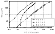
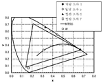
도 16은 발광 소자 1 내지 3의 휘도-전류 밀도 특성을 나타낸 것이다.
도 17은 발광 소자 1 내지 3의 전류 효율-휘도 특성을 나타낸 것이다.
도 18은 발광 소자 1 내지 3의 휘도-전압 특성을 나타낸 것이다.
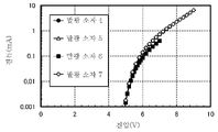
도 19는 발광 소자 1 내지 3의 전류-전압 특성을 나타낸 것이다.
도 20은 발광 소자 1 내지 3의 색도 좌표를 나타낸 것이다.
도 21은 비교 발광 소자 1 내지 3의 휘도-전류 밀도 특성을 나타낸 것이다.
도 22는 비교 발광 소자 1 내지 3의 전류 효율-휘도 특성을 나타낸 것이다.
도 23은 비교 발광 소자 1 내지 3의 휘도-전압 특성을 나타낸 것이다.
도 24는 비교 발광 소자 1 내지 3의 전류-전압 특성을 나타낸 것이다.
도 25는 비교 발광 소자 1 내지 3의 색도 좌표를 나타낸 것이다.
도 26은 1,6BnfAPrn-03의 톨루엔 용액에서의 1,6BnfAPrn-03의 발광 스펙트럼을 나타낸 것이다.
도 27은 발광 소자의 구조를 도시한 것이다.
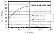
도 28은 발광 소자 4 내지 7의 휘도-전류 밀도 특성을 나타낸 것이다.
도 29는 발광 소자 4 내지 7의 전류 효율-휘도 특성을 나타낸 것이다.
도 30은 발광 소자 4 내지 7의 휘도-전압 특성을 나타낸 것이다.
도 31은 발광 소자 4 내지 7의 전류-전압 특성을 나타낸 것이다.
도 32는 발광 소자 4 내지 7의 색도 좌표를 나타낸 것이다.
도 33은 비교 발광 소자 4 내지 6의 휘도-전류 밀도 특성을 나타낸 것이다.
도 34는 비교 발광 소자 4 내지 6의 전류 효율-휘도 특성을 나타낸 것이다.
도 35는 비교 발광 소자 4 내지 6의 휘도-전압 특성을 나타낸 것이다.
도 36은 비교 발광 소자 4 내지 6의 전류-전압 특성을 나타낸 것이다.
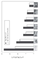
도 37은 실시예의 발광 장치를 나타낸 것이다.
도 38은 소비전력의 비교를 나타낸 것이다.
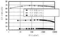
도 39는 발광 소자 8 및 9의 휘도-전류 밀도 특성을 나타낸 것이다.
도 40은 발광 소자 8 및 9의 전류 효율-휘도 특성을 나타낸 것이다.
도 41은 발광 소자 8 및 9의 휘도-전압 특성을 나타낸 것이다.
도 42는 발광 소자 8 및 9의 전류-전압 특성을 나타낸 것이다.
도 43은 발광 소자 8 및 9의 발광 스펙트럼을 나타낸 것이다.
도 44는 발광 소자 8 및 9의 정규화 휘도-시간 의존성 특성을 나타낸 것이다.1 (A) and (B) show a light emitting device, respectively.
2 shows a light emitting mechanism of a light emitting device.
3 shows a light emitting mechanism of a light emitting device.
4 shows a light emitting mechanism of a light emitting device.
5 shows a light emitting device.
6A and 6B show a light emitting device.
(A), (B), (C), (D), (D'-1), and (D'-2) of FIG. 7 illustrate an electronic device.
8A to 8C illustrate electronic devices.
9 shows a lighting device.
10 shows a light emitting device.
11(A) and (B) show an example of the touch panel of the embodiment.
12A and 12B show examples of the touch panel of the embodiment.
13(A) and (B) show an example of the touch panel of the embodiment.
14A and 14B are block diagrams and timing charts of the touch sensor.
15 is a circuit diagram of a touch sensor.
16 shows luminance-current density characteristics of light emitting
17 shows current efficiency-luminance characteristics of light emitting
18 shows luminance-voltage characteristics of light emitting
19 shows current-voltage characteristics of light emitting
20 shows chromaticity coordinates of light emitting
21 shows luminance-current density characteristics of Comparative Light-emitting
22 shows current efficiency-luminance characteristics of Comparative Light-emitting
23 shows luminance-voltage characteristics of Comparative Light-Emitting
24 shows current-voltage characteristics of Comparative Light-emitting
25 shows chromaticity coordinates of comparative
26 shows the emission spectrum of 1,6BnfAPrn-03 in toluene solution of 1,6BnfAPrn-03.
27 shows the structure of a light emitting device.
28 shows the luminance-current density characteristics of the
29 shows current efficiency-luminance characteristics of light emitting
30 shows the luminance-voltage characteristics of the
31 shows current-voltage characteristics of light emitting
32 shows chromaticity coordinates of light emitting
33 shows luminance-current density characteristics of comparative
34 shows current efficiency-luminance characteristics of comparative
35 shows luminance-voltage characteristics of comparative
36 shows current-voltage characteristics of comparative
Fig. 37 shows the light emitting device of the embodiment.
38 shows a comparison of power consumption.
39 shows the luminance-current density characteristics of the
40 shows current efficiency-luminance characteristics of light emitting
41 shows the luminance-voltage characteristics of the
42 shows current-voltage characteristics of light emitting
43 shows emission spectra of light emitting
44 shows normalized luminance-time dependence characteristics of light emitting
본 발명의 실시형태에 대하여 도면을 참조하여 이하에서 자세히 설명한다. 다만, 본 발명은 이하의 설명에 한정되지 않고, 본 발명의 취지 및 범위에서 벗어남이 없이 다양한 변경 및 수정이 가해질 수 있다. 따라서, 본 발명은 이하의 실시형태의 설명에 한정하여 해석되는 것이 아니다. DETAILED DESCRIPTION OF THE PREFERRED EMBODIMENTS Embodiments of the present invention will be described in detail below with reference to the drawings. However, the present invention is not limited to the following description, and various changes and modifications may be made without departing from the spirit and scope of the present invention. Therefore, this invention is limited to description of the following embodiment and is not interpreted.
또한, '막' 및 '층'이라는 용어는 경우 또는 상황에 따라 서로 교체될 수 있다. 예를 들어, '도전층'이라는 용어 대신에 '도전막'이라는 용어를 사용할 수 있고, '절연막'이라는 용어 대신에 '절연층'이라는 용어를 사용할 수 있다. In addition, the terms 'film' and 'layer' may be interchanged with each other depending on the case or situation. For example, the term 'conductive film' may be used instead of the term 'conductive layer', and the term 'insulating layer' may be used instead of the term 'insulating film'.
(실시형태 1)(Embodiment 1)
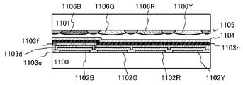
본 발명의 일 형태에 따른 발광 장치에는, 발광층을 포함하는 EL층이 한 쌍의 전극 사이에 제공된 발광 소자를 사용한다. 발광 소자에는 다양한 구조를 채용할 수 있고, 예를 들어 한 쌍의 전극 사이에 하나의 EL층이 제공된 구조(싱글 구조) 또는 전하 발생층을 개재하여 복수의 EL층이 적층된 구조(탠덤 구조)를 채용할 수 있다. 발광 소자의 소자 구조의 일례로서, 2개의 EL층을 포함하는 탠덤 구조의 발광 소자에 대하여 도 1의 (A)를 참조하여 이하에서 설명한다. In the light emitting device according to one embodiment of the present invention, a light emitting element in which an EL layer including a light emitting layer is provided between a pair of electrodes is used. Various structures can be employed for the light emitting element, for example, a structure in which one EL layer is provided between a pair of electrodes (single structure) or a structure in which a plurality of EL layers are stacked with a charge generating layer interposed (tandem structure) can be employed As an example of the element structure of the light emitting element, a light emitting element having a tandem structure including two EL layers will be described below with reference to FIG. 1A .
도 1의 (A)에 도시된 발광 소자는 발광층을 각각 포함하는 2개의 EL층(103a 및 103b)이 한 쌍의 전극(제 1 전극(101) 및 제 2 전극(102)) 사이에 제공된 구조를 가진다. EL층(103a)에서는, 정공 주입층(104a), 정공 수송층(105a), 발광층(106a), 전자 수송층(107a), 및 전자 주입층(108a) 등이 제 1 전극(101) 위에 순차적으로 적층되어 있다. EL층(103b)에서는, 정공 주입층(104b), 정공 수송층(105b), 발광층(106b), 전자 수송층(107b), 및 전자 주입층(108b) 등이 제 1 전극(101) 위에 순차적으로 적층되어 있다. 전하 발생층(109)이 EL층(103a)과 EL층(103b) 사이에 제공된다.
The light emitting element shown in Fig. 1A has a structure in which two
발광층들(106a 및 106b)은 각각 발광 물질 등의 복수의 물질을 적절한 조합으로 함유하며, 원하는 발광색의 형광 또는 인광을 방출할 수 있다. 또한, 발광층(106a 또는 106b) 상에, 발광층(106a 또는 106b)과는 다른 발광 물질을 함유하는 발광층을 더 제공하여도 좋다.
The
전하 발생층(109)은, 제 1 전극(101)과 제 2 전극(102) 사이에 전압이 인가되었을 때에, EL층들 중 한쪽(103a 또는 103b)에 전자를 주입하고, EL층들 중 다른 쪽(103b 또는 103a)에 정공을 주입하는 기능을 가진다. 따라서, 도 1의 (A)에서는, 제 1 전극(101)의 전위가 제 2 전극(102)의 전위보다 높아지도록 전압을 인가하면, 전하 발생층(109)이 EL층(103a)에 전자를 주입하고, EL층(103b)에 정공을 주입한다.
The
또한, 광 추출 효율에 관하여, 전하 발생층(109)은 가시광에 대하여 투광성을 가지는 것이 바람직하다(구체적으로는, 전하 발생층(109)의 가시광 투과율이 40% 이상). 전하 발생층(109)은 제 1 전극(101) 또는 제 2 전극(102)보다 도전율이 낮아도 기능한다.
In addition, with respect to light extraction efficiency, it is preferable that the
도 1의 (A)에 도시된 발광 소자에서는, EL층(103a 및 103b)에 포함되는 발광층(106a 및 106b)으로부터 모든 방향으로 방출되는 광이, 미소 광공진기(마이크로캐비티)로서 기능하는 제 1 전극(반사 전극)(101) 및 제 2 전극(반투과·반반사 전극)(102)에 의하여 공진될 수 있다. 광은 제 2 전극(102)을 통하여 방출된다. 제 1 전극(101)은 반사 전극이며, 반사 도전 재료와 투명 도전 재료의 적층 구조를 가진다. 그 광학 조정은 투명 도전막의 두께를 제어함으로써 행한다. 광학 조정은 EL층(103a)에 포함되는 정공 주입층(104a)의 두께를 제어함으로써 행하여도 좋다.
In the light emitting element shown in Fig. 1A, the light emitted in all directions from the
상술한 바와 같이, 제 1 전극(101) 또는 정공 주입층(104a)의 두께를 제어하여 광학 조정을 행함으로써, 발광층(106a 및 106b)으로부터 얻어지는 복수의 단색광선의 스펙트럼을 좁힐 수 있고, 색 순도가 높은 발광을 얻을 수 있다.
As described above, by performing optical adjustment by controlling the thickness of the
도 1의 (A)에 도시된 발광 소자에서, 반투과·반반사 전극으로서 기능하는 제 2 전극(102)과, 제 2 전극(102)에 가장 가까운 EL층(103b)의 발광 영역 사이의 광로 길이는 λ/4보다 작은 것이 바람직하고, 여기서 λ는 발광 영역으로부터 방출되는 광의 파장이다. 여기서, 발광 영역은 정공과 전자가 재결합되는 영역을 의미한다. 이러한 구조에 의하여, 도 1의 (A)에 도시된 발광 소자의 발광층(106a 및 106b)으로부터의 복수의 단색광선의 조합에 의하여 표준 백색의 광을 얻을 수 있다. 발광층(106a 및 106b)은 예를 들어, 청색의 광(예를 들어, 400nm 내지 480nm의 범위, 바람직하게는 450nm 내지 470nm의 범위에 발광 스펙트럼 피크를 가짐), 녹색의 광(예를 들어, 500nm 내지 560nm의 범위, 바람직하게는 520nm 내지 555nm의 범위에 발광 스펙트럼 피크를 가짐), 적색의 광(예를 들어, 580nm 내지 680nm의 범위, 바람직하게는 600nm 내지 620nm의 범위에 발광 스펙트럼 피크를 가짐), 주황색의 광(예를 들어, 580nm 내지 610nm의 범위, 바람직하게는 600nm 내지 610nm의 범위에 발광 스펙트럼 피크를 가짐), 또는 황색의 광(예를 들어, 555nm 내지 590nm의 범위, 바람직하게는 570nm 내지 580nm의 범위에 발광 스펙트럼 피크를 가짐)을 방출한다. 또한, 발광층(106a 및 106b)의 발광색의 구체적인 조합(106a/106b)으로서 다음에 기재된 것을 들 수 있다: 청색/녹색, 청색/황색, 청색/적색, 녹색/청색, 녹색/황색, 녹색/적색, 적색/청색, 적색/녹색, 및 적색/황색이다.
In the light emitting element shown in Fig. 1A, an optical path between the
다음에, 상술한 발광 소자를 제작하는 구체적인 예를 설명한다. Next, a specific example of manufacturing the above-described light emitting device will be described.
제 1 전극(101)은 반사 전극이기 때문에, 반사성을 가지는 도전 재료를 사용하여 형성되며, 가시광 반사율이 40% 이상 100% 이하, 바람직하게는 70% 이상 100% 이하이고 저항률이 1×10⁻²Ωcm 이하인 막을 사용한다. 제 2 전극(102)은 반사성을 가지는 도전 재료 및 투광성을 가지는 도전 재료를 사용하여 형성되며, 가시광 반사율이 20% 이상 80% 이하, 바람직하게는 40% 이상 70% 이하이고 저항률이 1×10⁻²Ωcm 이하인 막을 사용한다.Since the
제 1 전극(101)과 제 2 전극(102) 사이의 광로 길이는, 발광층(106a 및 106b)으로부터의 원하는 파장의 광이 공진하여 강화될 수 있도록, 원하는 광의 파장마다 조정된다. 구체적으로는, 제 1 전극(101)의 일부에 사용되는 투명 도전막의 두께를 변경하여, 전극들 사이의 거리가 mλ/2(m은 자연수)(여기서 λ는 원하는 광의 파장)가 되도록 한다.The optical path length between the
또한, 원하는 파장의 광을 강화시키기 위하여, 제 1 전극(101)과, 원하는 파장의 광을 방출하는 발광층(106a 및 106b) 사이의 광로 길이를 조정한다. 구체적으로는, 제 1 전극(101)의 일부에 사용될 수 있는 투명 도전막의 두께 또는 정공 주입층(104a)을 형성하는 유기막의 두께를 변경하여, 광로 길이가 (2m'+1)λ/4(m'은 자연수)(여기서 λ는 원하는 광의 파장)가 되도록 한다.In addition, in order to intensify light of a desired wavelength, the optical path length between the
이 경우, 제 1 전극(101)과 제 2 전극(102) 사이의 광로 길이는, 엄밀하게는 제 1 전극(101)의 반사 영역에서 제 2 전극(102)의 반사 영역까지의 총 두께로 표현된다. 그러나, 제 1 전극(101)과 제 2 전극(102)의 반사 영역은 정확하게 알아내기 어렵기 때문에, 반사 영역을 제 1 전극(101) 및 제 2 전극(102)의 어디에 설정하여도, 상술한 효과를 충분히 얻을 수 있는 것으로 한다. 또한, 제 1 전극(101)과 원하는 광을 방출하는 발광층 사이의 광로 길이는, 엄밀하게는 제 1 전극(101)의 반사 영역과 원하는 광을 방출하는 발광층의 발광 영역 사이의 광로 길이이다. 그러나, 제 1 전극(101)의 반사 영역과 원하는 광을 방출하는 발광층의 발광 영역은 정확하게 알아내기 어렵기 때문에, 반사 영역 및 발광 영역을 제 1 전극(101) 및 원하는 광을 방출하는 발광층의 어디에 설정하여도, 상술한 효과를 충분히 얻을 수 있는 것으로 한다.
In this case, the optical path length between the
제 1 전극(101) 및 제 2 전극(102)에는, 금속, 합금, 전기 전도성 화합물, 및 이들의 혼합물 등 중 어느 것을 적절히 사용할 수 있다. 구체적인 예로서는 산화 인듐-산화 주석(인듐 주석 산화물), 실리콘 또는 산화 실리콘을 함유하는 산화 인듐-산화 주석, 산화 인듐-산화 아연(인듐 아연 산화물), 산화 텅스텐 및 산화 아연을 함유하는 산화 인듐, 금(Au), 백금(Pt), 니켈(Ni), 텅스텐(W), 크로뮴(Cr), 몰리브데넘(Mo), 철(Fe), 코발트(Co), 구리(Cu), 팔라듐(Pd), 및 타이타늄(Ti)이 있다. 또한, 주기율표의 1족 또는 2족에 속하는 원소, 예를 들어 리튬(Li) 또는 세슘(Cs) 등의 알칼리 금속, 칼슘(Ca) 또는 스트론튬(Sr) 등의 알칼리 토금속, 마그네슘(Mg), 이러한 원소를 함유하는 합금(MgAg, AlLi), 유로퓸(Eu) 또는 이터븀(Yb) 등의 희토류 금속, 이러한 원소를 함유하는 합금, 및 그래핀 등을 사용할 수 있다. 제 1 전극(101) 및 제 2 전극(102)은, 예를 들어 스퍼터링법 또는 증착법(진공 증착법을 포함함)에 의하여 형성할 수 있다.
For the
정공 주입층(104a 및 104b)은 정공 수송성이 높은 정공 수송층(105a 및 105b)을 통하여 발광층(106a 및 106b)에 정공을 주입하며, 산화 몰리브데넘, 산화 바나듐, 산화 루테늄, 산화 텅스텐, 또는 산화 망가니즈 등의 억셉터 재료를 사용하여 형성할 수 있다. 또는, 정공 주입층(104a 및 104b)은 프탈로사이아닌(약칭: H2Pc) 또는 구리 프탈로사이아닌(약칭: CuPc) 등의 프탈로사이아닌계 화합물, 4,4'-비스[N-(4-다이페닐아미노페닐)-N-페닐아미노]바이페닐(약칭: DPAB) 또는 N,N'-비스{4-[비스(3-메틸페닐)아미노]페닐}-N,N'-다이페닐-(1,1'-바이페닐)-4,4'-다이아민(약칭: DNTPD) 등의 방향족 아민 화합물, 7,7,8,8-테트라사이아노-2,3,5,6-테트라플루오로퀴노다이메테인(약칭: F4-TCNQ), 클로라닐, 또는 2,3,6,7,10,11-헥사사이아노-1,4,5,8,9,12-헥사아자트라이페닐렌(약칭: HAT-CN) 등의 전자 흡인기(할로젠 또는 사이아노기)를 함유하는 화합물, 또는 폴리(3,4-에틸렌다이옥시싸이오펜)/폴리(스타이렌설폰산)(약칭: PEDOT/PSS) 등의 유기 억셉터 재료를 사용하여 형성할 수 있다.The
정공 주입층(104a 및 104b)은 정공 수송 재료 및 억셉터 물질을 함유하여도 좋다. 정공 주입층(104a 및 104b)이 정공 수송 재료 및 억셉터 물질을 함유하면, 억셉터 물질에 의하여 정공 수송 재료로부터 전자가 추출되어 정공이 발생되고, 정공 수송층(105a 및 105b)을 통하여 발광층(106a 및 106b)에 정공이 주입된다. 정공 수송층(105a 및 105b)은 정공 수송 재료를 사용하여 형성한다.
The
정공 주입층(104a 및 104b) 및 정공 수송층(105a 및 105b)에 사용되는 정공 수송 재료의 구체적인 예에는, 4,4'-비스[N-(1-나프틸)-N-페닐아미노]바이페닐(약칭: NPB 또는 α-NPD), N,N'-비스(3-메틸페닐)-N,N'-다이페닐-[1,1'-바이페닐]-4,4'-다이아민(약칭: TPD), 4,4',4''-트리스(카바졸-9-일)트라이페닐아민(약칭: TCTA), 4,4',4''-트리스(N,N-다이페닐아미노)트라이페닐아민(약칭: TDATA), 4,4',4''-트리스[N-(3-메틸페닐)-N-페닐아미노]트라이페닐아민(약칭: MTDATA), 및 4,4'-비스[N-(스파이로-9,9'-바이플루오렌-2-일)-N-페닐아미노]바이페닐(약칭: BSPB) 등의 방향족 아민 화합물; 3-[N-(9-페닐카바졸-3-일)-N-페닐아미노]-9-페닐카바졸(약칭: PCzPCA1); 3,6-비스[N-(9-페닐카바졸-3-일)-N-페닐아미노]-9-페닐카바졸(약칭: PCzPCA2); 및 3-[N-(1-나프틸)-N-(9-페닐카바졸-3-일)아미노]-9-페닐카바졸(약칭: PCzPCN1)이 포함된다. 다른 예에는 4,4'-다이(N-카바졸일)바이페닐(약칭: CBP), 1,3,5-트리스[4-(N-카바졸일)페닐]벤젠(약칭: TCPB), 및 9-[4-(10-페닐-9-안트라센일)페닐]-9H-카바졸(약칭: CzPA) 등의 카바졸 유도체가 포함된다. 여기서 열거한 물질은 주로 정공 이동도가 10-6cm2/Vs 이상인 물질이다. 또한, 전자 수송성보다 정공 수송성이 높기만 하면, 여기서 열거한 물질 외의 어떤 물질을 사용하여도 좋다.Specific examples of the hole transport material used for the hole injection layers 104a and 104b and the hole transport layers 105a and 105b include 4,4'-bis[ N- (1-naphthyl) -N -phenylamino]biphenyl (abbreviation: NPB or α-NPD), N , N' -bis(3-methylphenyl) -N , N' -diphenyl-[1,1'-biphenyl]-4,4'-diamine (abbreviation: TPD), 4,4',4''-tris(carbazol-9-yl)triphenylamine (abbreviation: TCTA), 4,4',4''-tris( N , N -diphenylamino)tri Phenylamine (abbreviation: TDATA), 4,4′,4′-tris[ N- (3-methylphenyl) -N -phenylamino]triphenylamine (abbreviation: MTDATA), and 4,4′-bis[ N Aromatic amine compounds, such as -(spiro-9,9'-bifluoren-2-yl) -N -phenylamino]biphenyl (abbreviation: BSPB); 3-[ N- (9-phenylcarbazol-3-yl) -N -phenylamino]-9-phenylcarbazole (abbreviation: PCzPCA1); 3,6-bis[ N- (9-phenylcarbazol-3-yl) -N -phenylamino]-9-phenylcarbazole (abbreviation: PCzPCA2); and 3-[ N- (1-naphthyl)-N-(9-phenylcarbazol-3-yl)amino]-9-phenylcarbazole (abbreviated as PCzPCN1 ). Other examples include 4,4′-di( N -carbazolyl)biphenyl (abbreviated CBP), 1,3,5-tris[4-( N -carbazolyl)phenyl]benzene (abbreviated TCPB), and 9 and carbazole derivatives such as -[4-(10-phenyl-9-anthracenyl)phenyl]-9H-carbazole (abbreviation: CzPA ). The materials listed here are mainly materials with hole mobility of 10 -6 cm 2 /Vs or more. In addition, any substance other than the substances enumerated herein may be used as long as the hole transporting property is higher than the electron transporting property.
다른 예에는, 폴리(N-바이닐카바졸)(약칭: PVK), 폴리(4-바이닐트라이페닐아민)(약칭: PVTPA), 폴리[N-(4-{N'-[4-(4-다이페닐아미노)페닐]페닐-N'-페닐아미노}페닐)메타크릴아마이드](약칭: PTPDMA), 및 폴리[N,N'-비스(4-뷰틸페닐)-N,N'-비스(페닐)벤지딘](약칭: Poly-TPD) 등의 고분자 화합물이 포함된다.Other examples include poly( N -vinylcarbazole) (abbreviated PVK), poly(4-vinyltriphenylamine) (abbreviated PVTPA), poly[ N- (4-{ N '-[4-(4-) diphenylamino)phenyl]phenyl- N' -phenylamino}phenyl)methacrylamide] (abbreviation: PTPDMA), and poly[ N , N' -bis(4-butylphenyl) -N , N' -bis(phenyl) ) benzidine] (abbreviation: Poly-TPD) and the like.
정공 주입층(105a 및 105b)에 사용되는 억셉터 물질의 예에는, 상술한 억셉터 재료 및 유기 억셉터 재료가 포함된다. 그 중에서, 주기율표의 4족 내지 8족 중 어느 것에 속하는 금속의 산화물을 사용하는 것이 바람직하고, 특히 산화 몰리브데넘을 사용하는 것이 바람직하다.
Examples of the acceptor material used for the
발광층들(106a 및 106b)은 각각 발광 물질을 함유한다. 발광층들(106a 및 106b)은 각각 발광 물질에 더하여, 유기 화합물인 전자 수송 재료 및/또는 정공 수송 재료를 함유하고, 본 발명의 일 형태에 따른 발광 소자에서는, 발광층들(106a 및 106b) 중 한쪽이, 형광 물질의 톨루엔 용액에서의 발광 스펙트럼의 피크 파장이 440nm 내지 460nm, 바람직하게는 440nm 내지 455nm인 형광 물질, 또는 2개의 벤조[b]나프토[1,2-d]퓨란일아민 골격이 피렌 골격에 결합된 유기 화합물을 함유한다. 형광 물질의 발광 스펙트럼의 반치폭은 20nm 이상 50nm 이하인 것이 바람직하다.The
톨루엔 용액에서의 발광 스펙트럼의 피크 파장이 440nm 내지 460nm인 형광 물질로서는 예를 들어, 방향족 다이아민 골격을 가지는 물질을 사용하는 것이 바람직하다. 더 바람직하게는, 피렌다이아민 골격을 가지는 물질을 사용한다. 피렌다이아민 골격을 가지는 물질로서 더 구체적으로는, 다음 일반식(G1)으로 표기되는, 2개의 벤조[b]나프토[1,2-d]퓨란일아민 골격이 피렌 골격에 결합된 유기 화합물을 사용하는 것이 바람직하다. 또한, 본 실시형태에서 사용될 수 있는 형광 물질은 이하의 예에 한정되지 않는다.As a fluorescent substance whose peak wavelength of the emission spectrum in a toluene solution is 440 nm - 460 nm, it is preferable to use the substance which has an aromatic diamine skeleton, for example. More preferably, a material having a pyrenediamine skeleton is used. As a material having a pyrene diamine skeleton, more specifically, an organic compound in which two benzo[ b ]naphtho[1,2- d ]furanylamine skeletons are bonded to a pyrene skeleton, represented by the following general formula (G1) It is preferable to use In addition, the fluorescent substance which can be used in this embodiment is not limited to the following example.
2개의 벤조[b]나프토[1,2-d]퓨란일아민 골격이 피렌 골격에 결합된 유기 화합물로서는, 다음 일반식(G1)으로 표기되는 유기 화합물을 사용할 수 있다. 또한, 다음 일반식(G1)으로 표기되는 유기 화합물은 청색 형광을 나타낸다.As an organic compound in which two benzo[ b ]naphtho[1,2- d ]furanylamine skeletons are bonded to a pyrene skeleton, an organic compound represented by the following general formula (G1) can be used. In addition, the organic compound represented by the following general formula (G1) exhibits blue fluorescence.

일반식(G1)에 있어서, Ar1 및 Ar2는 각각 독립적으로, 고리를 형성하는 치환 또는 비치환된 탄소수 6 내지 13의 아릴기를 나타내고; R1 내지 R8, R10 내지 R18, 및 R20 내지 R28은 각각 독립적으로, 수소, 치환 또는 비치환된 탄소수 1 내지 6의 알킬기, 치환 또는 비치환된 탄소수 1 내지 6의 알콕시기, 사이아노기, 할로젠, 치환 또는 비치환된 탄소수 1 내지 6의 할로알킬기, 또는 치환 또는 비치환된 탄소수 6 내지 10의 아릴기를 나타낸다.In the general formula (G1), Ar 1 and Ar 2 each independently represent a substituted or unsubstituted aryl group having 6 to 13 carbon atoms to form a ring; R 1 to R 8 , R 10 to R 18 , and R 20 to R 28 are each independently hydrogen, a substituted or
일반식(G1)으로 표기되는 유기 화합물의 구체적인 예에 대해서는 실시형태 2를 참조할 수 있다.
발광층들(106a 및 106b) 중 다른 쪽의 발광 물질로서 사용할 수 있는 재료에 특별한 한정은 없고, 단일항 여기 에너지를 가시광 영역의 발광으로 변환하는 발광 재료, 또는 삼중항 여기 에너지를 가시광 영역의 발광으로 변환하는 발광 재료를 사용할 수 있다.
There is no particular limitation on the material that can be used as the light emitting material of the other of the
단일항 여기 에너지를 가시광 영역의 발광으로 변환하는 발광 재료의 예로서, 형광을 방출하는 물질을 들 수 있다. 형광을 방출하는 물질의 예에는, 피렌 유도체, 안트라센 유도체, 트라이페닐렌 유도체, 플루오렌 유도체, 카바졸 유도체, 다이벤조싸이오펜 유도체, 다이벤조퓨란 유도체, 다이벤조퀴녹살린 유도체, 퀴녹살린 유도체, 피리딘 유도체, 피리미딘 유도체, 페난트렌 유도체, 및 나프탈렌 유도체가 포함된다. 피렌 유도체는 발광 양자 수율이 높으므로 특히 바람직하다. 피렌 유도체의 구체적인 예에는, N,N'-비스(3-메틸페닐)-N,N'-비스[3-(9-페닐-9H-플루오렌-9-일)페닐]피렌-1,6-다이아민(1,6mMemFLPAPrn), N,N'-비스[4-(9-페닐-9H-플루오렌-9-일)페닐]-N,N'-다이페닐피렌-1,6-다이아민(1,6FLPAPrn), N,N'-비스(다이벤조퓨란-2-일)-N,N'-다이페닐피렌-1,6-다이아민(1,6FrAPrn), 및 N,N'-비스(다이벤조싸이오펜-2-일)-N,N'-다이페닐피렌-1,6-다이아민(1,6ThAPrn)이 포함된다.As an example of a light-emitting material that converts singlet excitation energy into light emission in the visible region, a material that emits fluorescence is exemplified. Examples of substances emitting fluorescence include pyrene derivatives, anthracene derivatives, triphenylene derivatives, fluorene derivatives, carbazole derivatives, dibenzothiophene derivatives, dibenzofuran derivatives, dibenzoquinoxaline derivatives, quinoxaline derivatives, pyridine derivatives, pyrimidine derivatives, phenanthrene derivatives, and naphthalene derivatives. A pyrene derivative is particularly preferable because of its high emission quantum yield. Specific examples of the pyrene derivative include N , N' -bis(3-methylphenyl) -N , N' -bis[3-(9-phenyl- 9H -fluoren-9-yl)phenyl]pyrene-1,6 -Diamine ( 1,6mMemFLPAPrn ), N , N' -bis[4-(9-phenyl-9H-fluoren-9-yl)phenyl] -N , N' -diphenylpyrene-1,6-dia Min(1,6FLPAPrn), N , N' -bis(dibenzofuran-2-yl) -N , N' -diphenylpyrene-1,6-diamine (1,6FrAPrn), and N , N'- bis(dibenzothiophen-2-yl) -N , N' -diphenylpyrene-1,6-diamine (1,6ThAPrn).
삼중항 여기 에너지를 가시광 영역의 발광으로 변환하는 발광 재료의 예에는, 인광을 방출하는 물질 및 열활성화 지연 형광(TADF) 재료가 포함된다. 또한, TADF 재료는, 삼중항 여기 상태를 적은 열 에너지를 사용하여 단일항 여기 상태로 업컨버트(up-convert)할 수 있고(즉, 역항간 교차가 가능), 단일항 여기 상태로부터 효율적으로 발광(형광)을 나타낸다. TADF는, 삼중항 여기 준위와 단일항 여기 준위의 에너지 차이가 0eV 이상 0.2eV 이하, 바람직하게는 0eV 이상 0.1eV 이하인 조건하에서 효율적으로 얻어진다. 또한, TADF에 의하여 나타내어지는 "지연 형광"은 통상의 형광과 동일한 스펙트럼을 가지며 수명이 매우 긴 발광을 말한다. 그 수명은 10-6초 이상, 바람직하게는 10-3초 이상이다.Examples of luminescent materials that convert triplet excitation energy into luminescence in the visible region include materials that emit phosphorescence and thermally activated delayed fluorescence (TADF) materials. In addition, TADF materials can up-convert triplet excited states to singlet excited states using little thermal energy (i.e., inverse-to-inverse crossover is possible) and efficiently emit light from singlet excited states. (fluorescence) is shown. TADF is efficiently obtained under the condition that the energy difference between the triplet excitation level and the singlet excitation level is 0 eV or more and 0.2 eV or less, preferably 0 eV or more and 0.1 eV or less. In addition, "delayed fluorescence" represented by TADF refers to light emission having the same spectrum as normal fluorescence and having a very long lifetime. Its lifetime is at least 10 -6 seconds, preferably at least 10 -3 seconds.
인광을 방출하는 물질로서는, 이리듐계, 로듐계, 또는 백금계의 유기 금속 착체 또는 금속 착체를 사용할 수 있고, 특히 이리듐계 오쏘 메탈 착체 등의 유기 이리듐 착체가 바람직하다. 오쏘메탈화 리간드로서는 4H-트라이아졸 리간드, 1H-트라이아졸 리간드, 이미다졸 리간드, 피리딘 리간드, 피리미딘 리간드, 피라진 리간드, 및 아이소퀴놀린 리간드 등을 들 수 있다. 금속 착체로서는, 포르피린 리간드를 가지는 백금 착체 등을 들 수 있다. 인광을 방출하는 물질의 예에는, 비스[2-(3',5'-비스트라이플루오로메틸페닐)피리디네이토-N,C 2' ]이리듐(III)피콜리네이트(약칭: Ir(CF3ppy)2(pic)), 비스[2-(4',6'-다이플루오로페닐)피리디네이토-N,C 2 ']이리듐(III)아세틸아세토네이트(약칭: FIracac), 트리스(2-페닐피리디네이토)이리듐(III)(약칭: Ir(ppy)3), 비스(2-페닐피리디네이토)이리듐(III)아세틸아세토네이트(약칭: Ir(ppy)2(acac)), 트리스(아세틸아세토네이토)(모노페난트롤린)터븀(III)(약칭: Tb(acac)3(Phen)), 비스(벤조[h]퀴놀리네이토)이리듐(III)아세틸아세토네이트(약칭: Ir(bzq)2(acac)), 비스(2,4-다이페닐-1,3-옥사졸레이토-N,C 2 ')이리듐(III)아세틸아세토네이트(약칭: Ir(dpo)2(acac)), 비스{2-[4'-(퍼플루오로페닐)페닐]피리디네이토-N,C 2 '}이리듐(III)아세틸아세토네이트(약칭: Ir(p-PF-ph)2(acac)), 비스(2-페닐벤조싸이아졸레이토-N,C 2 ')이리듐(III)아세틸아세토네이트(약칭: Ir(bt)2(acac)), 비스[2-(2'-벤조[4,5-α]싸이엔일)피리디네이토-N,C 3']이리듐(III)아세틸아세토네이트(약칭: Ir(btp)2(acac)), 비스(1-페닐아이소퀴놀리네이토-N,C 2')이리듐(III)아세틸아세토네이트(약칭: Ir(piq)2(acac)), (아세틸아세토네이토)비스[2,3-비스(4-플루오로페닐)퀴녹살리네이토]이리듐(III)(약칭: Ir(Fdpq)2(acac)), (아세틸아세토네이토)비스(3,5-다이메틸-2-페닐피라지네이토)이리듐(III)(약칭: [Ir(mppr-Me)2(acac)]), (아세틸아세토네이토)비스(5-아이소프로필-3-메틸-2-페닐피라지네이토)이리듐(III)(약칭: [Ir(mppr-iPr)2(acac)]), (아세틸아세토네이토)비스(2,3,5-트라이페닐피라지네이토)이리듐(III)(약칭: Ir(tppr)2(acac)), 비스(2,3,5-트라이페닐피라지네이토)(다이피발로일메타네이토)이리듐(III)(약칭: [Ir(tppr)2(dpm)]), (아세틸아세토네이토)비스(6-tert-뷰틸-4-페닐피리미디네이토)이리듐(III)(약칭: [Ir(tBuppm)2(acac)]), (아세틸아세토네이토)비스(4,6-다이페닐피리미디네이토)이리듐(III)(약칭: [Ir(dppm)2(acac)]), 2,3,7,8,12,13,17,18-옥타에틸-21H,23H-포르피린 백금(II)(약칭: PtOEP), 트리스(1,3-다이페닐-1,3-프로페인다이오네이토)(모노페난트롤린)유로퓸(III)(약칭: Eu(DBM)3(Phen)), 및 트리스[1-(2-테노일)-3,3,3-트라이플루오로아세토네이토](모노페난트롤린)유로퓸(III)(약칭: Eu(TTA)3(Phen))이 포함된다.As the phosphorescence-emitting substance, an iridium-based, rhodium-based, or platinum-based organometallic complex or metal complex can be used, and an organic iridium complex such as an iridium-based orthometal complex is particularly preferable. Examples of the orthometalated ligand include 4H-triazole ligand, 1H - triazole ligand, imidazole ligand, pyridine ligand, pyrimidine ligand, pyrazine ligand, and isoquinoline ligand. As a metal complex, the platinum complex etc. which have a porphyrin ligand are mentioned. Examples of phosphorescent-emitting materials include bis[2-(3',5'-bistrifluoromethylphenyl)pyridinato- N , C2 ' ]iridium(III)picolinate (abbreviated as Ir(CF) 3 ppy) 2 (pic)), bis[2-(4',6'-difluorophenyl)pyridinato - N , C2 ' ]iridium(III)acetylacetonate (abbreviation: FIracac), tris (2-phenylpyridinato)iridium(III) (abbreviation: Ir(ppy) 3 ), bis(2-phenylpyridinato)iridium(III)acetylacetonate (abbreviation: Ir(ppy) 2 (acac) )), tris (acetylacetonato) (monophenanthroline) terbium (III) (abbreviation: Tb (acac) 3 (Phen)), bis (benzo [ h ] quinolinato) iridium (III) acetyl aceto nate (abbreviated: Ir(bzq) 2 (acac)), bis(2,4-diphenyl-1,3-oxazolato- N , C 2 ' )iridium(III)acetylacetonate (abbreviated: Ir(dpo) ) 2 (acac)), bis{2-[4′-(perfluorophenyl)phenyl]pyridinato - N , C2 ′ }iridium(III)acetylacetonate (abbreviation: Ir(p-PF-) ph) 2 (acac)), bis(2-phenylbenzothiazolato- N , C 2 ' )iridium(III)acetylacetonate (abbreviated: Ir(bt) 2 (acac)), bis[2-(2) '-benzo [4,5- α ] thienyl) pyridinato- N , C 3 ' ] iridium (III) acetylacetonate (abbreviation: Ir (btp) 2 (acac)), bis (1-phenyl Isoquinolinato- N , C2 ' )iridium(III)acetylacetonate (abbreviated: Ir(piq) 2 (acac)), (acetylacetonato)bis[2,3-bis(4-fluoro Phenyl) quinoxalinato] iridium (III) (abbreviation: Ir (Fdpq) 2 (acac)), (acetylacetonato) bis (3,5-dimethyl-2-phenylpyrazinato) iridium (III) (abbreviation: [Ir(mppr-Me) 2 (acac)]), (acetylacetonato)bis(5-isopropyl-3-methyl-2-phenylpyrazinato)iridium(III) (abbreviation: [Ir (mppr-iPr) 2 (acac)]), (acetylacetonato) Bis(2,3,5-triphenylpyrazinato)iridium(III) (abbreviation: Ir(tppr) 2 (acac)), bis(2,3,5-triphenylpyrazinato) (dipivaloyl Metanato) iridium (III) (abbreviation: [Ir(tppr) 2 (dpm)]), (acetylacetonato)bis(6- tert -butyl-4-phenylpyrimidinato)iridium (III) ( Abbreviation: [Ir(tBuppm) 2 (acac)]), (acetylacetonato)bis(4,6-diphenylpyrimidinato)iridium(III) (abbreviation: [Ir(dppm) 2 (acac)] ), 2,3,7,8,12,13,17,18- octaethyl -21H, 23H -porphyrin platinum(II) (abbreviation: PtOEP), tris(1,3-diphenyl-1,3 -propanedioneto) (monophenanthroline) europium (III) (abbreviated: Eu(DBM) 3 (Phen)), and tris[1-(2-thenoyl)-3,3,3-trifluoro roacetonato] (monophenanthroline) europium (III) (abbreviation: Eu(TTA) 3 (Phen)).
TADF 재료의 구체적인 예에는, 풀러렌, 그 유도체, 프로플라빈 등의 아크리딘 유도체, 및 에오신이 포함된다. 다른 예에는, 마그네슘(Mg), 아연(Zn), 카드뮴(Cd), 주석(Sn), 백금(Pt), 인듐(In), 또는 팔라듐(Pd)을 함유하는 포르피린 등의 금속 함유 포르피린이 포함된다. 금속 함유 포르피린의 예에는, 프로토포르피린-플루오린화 주석 착체(SnF2(Proto IX)), 메소포르피린-플루오린화 주석 착체(SnF2(Meso IX)), 헤마토포르피린-플루오린화 주석 착체(SnF2(Hemato IX)), 코프로포르피린 테트라메틸 에스터-플루오린화 주석 착체(SnF2(Copro III-4Me)), 옥타에틸포르피린-플루오린화 주석 착체(SnF2(OEP)), 에티오포르피린-플루오린화 주석 착체(SnF2(Etio I)), 및 옥타에틸포르피린-염화 백금 착체(PtCl2OEP)가 포함된다. 또는, 2-(바이페닐-4-일)-4,6-비스(12-페닐인돌로[2,3-a]카바졸-11-일)-1,3,5-트라이아진(PIC-TRZ) 등의 π전자 과잉 헤테로방향족 고리 및 π전자 부족 헤테로방향족 고리를 포함하는 헤테로고리 화합물을 사용할 수 있다. 또한, π전자 과잉 헤테로방향족 고리가 π전자 부족 헤테로방향족 고리에 직접 결합된 재료는, π전자 과잉 헤테로방향족 고리의 도너성 및 π전자 부족 헤테로방향족 고리의 억셉터성의 양쪽이 높아지고 S1 준위와 T1 준위의 에너지 차이가 작아지기 때문에, 특히 바람직하다.Specific examples of the TADF material include fullerene, its derivatives, acridine derivatives such as proplavin, and eosin. Other examples include metal-containing porphyrins, such as porphyrins containing magnesium (Mg), zinc (Zn), cadmium (Cd), tin (Sn), platinum (Pt), indium (In), or palladium (Pd). do. Examples of metal-containing porphyrins include protoporphyrin-tin fluoride complex (SnF 2 (Proto IX)), mesoporphyrin-tin fluoride complex (SnF 2 (Meso IX)), hematoporphyrin-tin fluoride complex (SnF 2 ) (Hemato IX)), coproporphyrin tetramethyl ester-fluorinated tin complex (SnF 2 (Copro III-4Me)), octaethylporphyrin-tin fluorinated complex (SnF 2 (OEP)), ethioporphyrin-fluorinated tin complex (SnF 2 (Etio I)), and octaethylporphyrin-platinum chloride complex (PtCl 2 OEP). or 2-(biphenyl-4-yl)-4,6-bis(12-phenylindolo[2,3-a]carbazol-11-yl)-1,3,5-triazine (PIC- TRZ) and the like can be used a heterocyclic compound including a π-electron-rich heteroaromatic ring and a π-electron-deficient heteroaromatic ring. In addition, the material in which the π-electron-rich heteroaromatic ring is directly bonded to the π-electron-deficient heteroaromatic ring increases both the donor property of the π-electron-rich heteroaromatic ring and the acceptor property of the π-electron-sufficient heteroaromatic ring, and the S 1 level and T Since the energy difference of 1 level becomes small, it is especially preferable.
발광층들(106a 및 106b) 중 다른 쪽의 발광 물질로서 사용할 수 있는 재료로서, 삼중항 여기 에너지를 가시광 영역의 발광으로 변환하는 발광 재료를 사용하는 것이 바람직하다. 더 바람직하게는, 황색 인광을 나타내는 인광 물질을 사용한다. 이러한 구조에 의하여, 소비전력이 낮은 발광 소자를 얻을 수 있다. 발광 장치의 표시 소자로서 이러한 발광 소자를 사용함으로써, 백색 발광을 얻을 때의 소비전력을 효과적으로 저감할 수 있다.
As a material usable as the light emitting material of the other of the
발광층(106a 및 106b)의 유기 화합물로서 전자 수송 재료를 사용하는 경우에는, 질소 함유 헤테로방향족 화합물 등의 π전자 부족 헤테로방향족 화합물이 바람직하고, 그 예에는 2-[3-(다이벤조싸이오펜-4-일)페닐]다이벤조[f,h]퀴녹살린(약칭: 2mDBTPDBq-II), 2-[3'-(다이벤조싸이오펜-4-일)바이페닐-3-일]다이벤조[f,h]퀴녹살린(약칭: 2mDBTBPDBq-II), 2-[4-(3,6-다이페닐-9H-카바졸-9-일)페닐]다이벤조[f,h]퀴녹살린(약칭: 2CzPDBq-III), 7-[3-(다이벤조싸이오펜-4-일)페닐]다이벤조[f,h]퀴녹살린(약칭: 7mDBTPDBq-II), 및 6-[3-(다이벤조싸이오펜-4-일)페닐]다이벤조[f,h]퀴녹살린(약칭: 6mDBTPDBq-II) 등의 퀴녹살린 유도체 및 다이벤조퀴녹살린 유도체가 포함된다.When an electron transporting material is used as the organic compound of the
발광층(106a 및 106b)의 유기 화합물로서 정공 수송 재료를 사용하는 경우에는, π전자 과잉 헤테로방향족 화합물(예를 들어, 카바졸 유도체 또는 인돌 유도체) 또는 방향족 아민 화합물이 바람직하고, 그 예에는 4-페닐-4'-(9-페닐-9H-카바졸-3-일)트라이페닐아민(약칭: PCBA1BP), 4,4'-다이(1-나프틸)-4''-(9-페닐-9H-카바졸-3-일)트라이페닐아민(약칭: PCBNBB), 3-[N-(1-나프틸)-N-(9-페닐카바졸-3-일)아미노]-9-페닐카바졸(약칭: PCzPCN1), 4,4',4''-트리스[N-(1-나프틸)-N-페닐아미노]트라이페닐아민(약칭: 1'-TNATA), 2,7-비스[N-(4-다이페닐아미노페닐)-N-페닐아미노]-스파이로-9,9'-바이플루오렌(약칭: DPA2SF), N,N'-비스(9-페닐카바졸-3-일)-N,N'-다이페닐벤젠-1,3-다이아민(약칭: PCA2B), N-(9,9-다이메틸-2-다이페닐아미노-9H-플루오렌-7-일)다이페닐아민(약칭: DPNF), N,N',N''-트라이페닐-N,N',N''-트리스(9-페닐카바졸-3-일)벤젠-1,3,5-트라이아민(약칭: PCA3B), 2-[N-(9-페닐카바졸-3-일)-N-페닐아미노]스파이로-9,9'-바이플루오렌(약칭: PCASF), 2-[N-(4-다이페닐아미노페닐)-N-페닐아미노]스파이로-9,9'-바이플루오렌(약칭: DPASF), N,N'-비스[4-(카바졸-9-일)페닐]-N,N'-다이페닐-9,9-다이메틸플루오렌-2,7-다이아민(약칭: YGA2F), 4,4'-비스[N-(3-메틸페닐)-N-페닐아미노]바이페닐(약칭: TPD), 4,4'-비스[N-(4-다이페닐아미노페닐)-N-페닐아미노]바이페닐(약칭: DPAB), N-(9,9-다이메틸-9H-플루오렌-2-일)-N-{9,9-다이메틸-2-[N'-페닐-N'-(9,9-다이메틸-9H-플루오렌-2-일)아미노]-9H-플루오렌-7-일}페닐아민(약칭: DFLADFL), 3-[N-(9-페닐카바졸-3-일)-N-페닐아미노]-9-페닐카바졸(약칭: PCzPCA1), 3-[N-(4-다이페닐아미노페닐)-N-페닐아미노]-9-페닐카바졸(약칭: PCzDPA1), 3,6-비스[N-(4-다이페닐아미노페닐)-N-페닐아미노]-9-페닐카바졸(약칭: PCzDPA2), 4,4'-비스(N-{4-[N'-(3-메틸페닐)-N'-페닐아미노]페닐}-N-페닐아미노)바이페닐(약칭: DNTPD), 3,6-비스[N-(4-다이페닐아미노페닐)-N-(1-나프틸)아미노]-9-페닐카바졸(약칭: PCzTPN2), 및 3,6-비스[N-(9-페닐카바졸-3-일)-N-페닐아미노]-9-페닐카바졸(약칭: PCzPCA2)이 포함된다.When a hole transporting material is used as the organic compound of the light emitting layers 106a and 106b, a π-electron excess heteroaromatic compound (eg, a carbazole derivative or an indole derivative) or an aromatic amine compound is preferable, for example, 4- Phenyl-4'-(9-phenyl-9H-carbazol-3-yl)triphenylamine (abbreviation: PCBA1BP ), 4,4'-di(1-naphthyl)-4''-(9-phenyl -9H-carbazol-3-yl)triphenylamine (abbreviation: PCBNBB ), 3-[ N- (1-naphthyl ) -N-(9-phenylcarbazol-3-yl)amino]-9- Phenylcarbazole (abbreviation: PCzPCN1), 4,4',4''-tris[ N- (1-naphthyl) -N -phenylamino]triphenylamine (abbreviation: 1'-TNATA), 2,7- Bis[ N- (4-diphenylaminophenyl) -N -phenylamino]-spiro-9,9'-bifluorene (abbreviation: DPA2SF), N , N' -bis(9-phenylcarbazole-3 -yl) -N , N' -diphenylbenzene-1,3-diamine (abbreviation: PCA2B ), N- (9,9-dimethyl-2-diphenylamino-9H-fluoren-7-yl ) diphenylamine (abbreviation: DPNF), N , N ', N ''-triphenyl- N , N ', N ''-tris(9-phenylcarbazol-3-yl)benzene-1,3,5 -Triamine (abbreviation: PCA3B), 2-[ N- (9-phenylcarbazol-3-yl) -N -phenylamino]spiro-9,9'-bifluorene (abbreviation: PCASF), 2- [ N- (4-diphenylaminophenyl) -N -phenylamino]spiro-9,9'-bifluorene (abbreviation: DPASF), N , N' -bis[4-(carbazol-9-yl) )phenyl] -N , N' -diphenyl-9,9-dimethylfluorene-2,7-diamine (abbreviation: YGA2F ), 4,4'-bis[ N- (3-methylphenyl)-N- Phenylamino]biphenyl (abbreviation: TPD), 4,4'-bis[ N- (4-diphenylaminophenyl) -N -phenylamino]biphenyl (abbreviation: DPAB), N- (9,9-di Methyl -9H-fluoren-2-yl)-N- { 9,9-dimethyl-2-[ N' -phenyl- N '-(9,9- dimethyl -9H-fluorene-2- yl)amino] -9H -fluoren-7-yl}phenyl Amine (abbreviation: DFLADFL), 3-[ N- (9-phenylcarbazol-3-yl) -N -phenylamino]-9-phenylcarbazole (abbreviation: PCzPCA1), 3-[ N- (4-di Phenylaminophenyl) -N -phenylamino]-9-phenylcarbazole (abbreviation: PCzDPA1), 3,6-bis[ N- (4-diphenylaminophenyl) -N -phenylamino]-9-phenylcarbazole (abbreviation: PCzDPA2), 4,4'-bis( N- {4-[ N '-(3-methylphenyl)-N'-phenylamino]phenyl} -N -phenylamino ) biphenyl (abbreviation: DNTPD), 3,6-bis[ N- (4-diphenylaminophenyl)-N-(1-naphthyl)amino]-9-phenylcarbazole (abbreviation: PCzTPN2), and 3,6-bis[ N- (9 ) -phenylcarbazol-3-yl) -N -phenylamino]-9-phenylcarbazole (abbreviation: PCzPCA2).
발광층에 사용하는 발광 물질이 인광을 방출하는 물질인 경우, 발광층에 사용하는 유기 화합물의 예에는 아연계 또는 알루미늄계 금속 착체, 옥사다이아졸 유도체, 트라이아졸 유도체, 벤즈이미다졸 유도체, 퀴녹살린 유도체, 다이벤조퀴녹살린 유도체, 다이벤조싸이오펜 유도체, 다이벤조퓨란 유도체, 피리미딘 유도체, 트라이아진 유도체, 피리딘 유도체, 바이피리딘 유도체, 및 페난트롤린 유도체에 더하여, 방향족 아민 및 카바졸 유도체가 포함된다. When the light emitting material used for the light emitting layer is a material that emits phosphorescence, examples of the organic compound used for the light emitting layer include zinc-based or aluminum-based metal complexes, oxadiazole derivatives, triazole derivatives, benzimidazole derivatives, quinoxaline derivatives, In addition to dibenzoquinoxaline derivatives, dibenzothiophene derivatives, dibenzofuran derivatives, pyrimidine derivatives, triazine derivatives, pyridine derivatives, bipyridine derivatives, and phenanthroline derivatives, aromatic amine and carbazole derivatives are included.
발광층에 사용하는 발광 물질이 형광을 방출하는 물질인 경우, S1 준위가 높고 T1 준위가 낮은 안트라센 유도체 또는 테트라센 유도체를 사용하는 것이 바람직하다. 구체적인 예에는, 9-페닐-3-[4-(10-페닐-9-안트릴)페닐]-9H-카바졸(PCzPA), 9-[4-(10-페닐-9-안트라센일)페닐]-9H-카바졸(CzPA), 7-[4-(10-페닐-9-안트릴)페닐]-7H-다이벤조[c,g]카바졸(cgDBCzPA), 6-[3-(9,10-다이페닐-2-안트릴)페닐]-벤조[b]나프토[1,2-d]퓨란(2mBnfPPA), 9-페닐-10-{4-(9-페닐-9H-플루오렌-9-일)바이페닐-4'-일}안트라센(FLPPA), 5,12-다이페닐테트라센, 및 5,12-비스(바이페닐-2-일)테트라센이 포함된다.When the light emitting material used for the light emitting layer is a material emitting fluorescence, it is preferable to use an anthracene derivative or a tetracene derivative having a high S 1 level and a low T 1 level. Specific examples include 9-phenyl-3-[4-(10-phenyl-9-anthryl)phenyl]-9H-carbazole ( PCzPA ), 9-[4-(10-phenyl-9-anthracenyl) Phenyl]-9H-carbazole ( CzPA ), 7-[4-(10-phenyl-9-anthryl)phenyl]-7H-dibenzo[ c , g ]carbazole ( cgDBCzPA ), 6-[3 -(9,10-diphenyl-2-anthryl)phenyl]-benzo[ b ]naphtho[1,2- d ]furan (2mBnfPPA), 9-phenyl-10-{4-(9-phenyl-9) H -fluoren-9-yl)biphenyl-4'-yl}anthracene (FLPPA), 5,12-diphenyltetracene, and 5,12-bis(biphenyl-2-yl)tetracene .
전자 수송층(107a 및 107b)은 전자 수송성이 높은 물질을 함유하는 층이다. 전자 수송층(107a 및 107b)에는 Alq3, 트리스(4-메틸-8-퀴놀리놀레이토)알루미늄(약칭: Almq3), 비스(10-하이드록시벤조[h]퀴놀리네이토)베릴륨(II)(약칭: BeBq2), BAlq, Zn(BOX)2, 또는 비스[2-(2-하이드록시페닐)벤조싸이아졸레이토]아연(II)(약칭: Zn(BTZ)2) 등의 금속 착체를 사용할 수 있다. 또한, 2-(4-바이페닐릴)-5-(4-tert-뷰틸페닐)-1,3,4-옥사다이아졸(약칭: PBD), 1,3-비스[5-(p-tert-뷰틸페닐)-1,3,4-옥사다이아졸-2-일]벤젠(약칭: OXD-7), 3-(4-tert-바이페닐릴)-4-페닐-5-(4-뷰틸페닐)-1,2,4-트라이아졸(약칭: TAZ), 3-(4-tert-뷰틸페닐)-4-(4-에틸페닐)-5-(4-바이페닐릴)-1,2,4-트라이아졸(약칭: p-EtTAZ), 바소페난트롤린(약칭: BPhen), 바소큐프로인(약칭: BCP), 또는 4,4'-비스(5-메틸벤즈옥사졸-2-일)스틸벤(약칭: BzOs) 등의 헤테로방향족 화합물을 사용할 수도 있다. 또는, 폴리(2,5-피리딘다이일)(약칭: PPy), 폴리[(9,9-다이헥실플루오렌-2,7-다이일)-co-(피리딘-3,5-다이일)](약칭: PF-Py), 또는 폴리[(9,9-다이옥틸플루오렌-2,7-다이일)-co-(2,2'-바이피리딘-6,6'-다이일)](약칭: PF-BPy) 등의 고분자 화합물을 사용할 수 있다. 여기서 언급한 물질은 주로 전자 이동도가 1×10⁻⁶cm2/Vs 이상인 물질이다. 그러나, 정공 수송성보다 전자 수송성이 높기만 하면, 상술한 물질 외의 어떤 물질을 전자 수송층(107a 및 107b)에 사용하여도 좋다.The
전자 수송층들(107a 및 107b) 각각은 단층에 한정되지 않고, 상술한 물질 중 어느 것을 함유하는 2개 이상의 층을 포함하는 적층이어도 좋다.
Each of the
전자 주입층(108a 및 108b)은 전자 주입성이 높은 물질을 함유하는 층이다. 전자 주입층(108a 및 108b)에는, 플루오린화 리튬(LiF), 플루오린화 세슘(CsF), 플루오린화 칼슘(CaF2), 또는 리튬 산화물(LiOx) 등의 알칼리 금속, 알칼리 토금속, 또는 이들의 화합물을 사용할 수 있다. 플루오린화 어븀(ErF3)과 같은 희토류 금속 화합물을 사용할 수도 있다. 전자화물(electride)을 전자 주입층(108a 및 108b)에 사용하여도 좋다. 전자화물의 예에는 산화 칼슘-산화 알루미늄에 전자가 고농도로 첨가된 물질이 포함된다. 상술한 전자 수송층(107a 및 107b)을 형성하기 위한 물질 중 어느 것을 사용할 수도 있다.The
전자 주입층들(108a 및 108b) 각각은 유기 화합물과 전자 공여체가 혼합된 복합 재료를 사용하여 형성되어도 좋다. 전자 공여체에 의하여 유기 화합물에 전자가 발생되기 때문에, 상기 복합 재료는 전자 주입성 및 전자 수송성이 우수하다. 이 경우, 유기 화합물은 발생된 전자의 수송이 우수한 재료인 것이 바람직하다. 구체적으로는 예를 들어 상술한 전자 수송층(107a 및 107b)을 형성하기 위한 물질(예를 들어, 금속 착체 또는 헤테로방향족 화합물)을 사용할 수 있다. 전자 공여체로서는, 유기 화합물에 대한 전자 도너성을 나타내는 물질을 사용하여도 좋다. 구체적으로는, 알칼리 금속, 알칼리 토금속, 및 희토류 금속이 바람직하고, 리튬, 세슘, 마그네슘, 칼슘, 어븀, 및 이터븀 등을 들 수 있다. 또한, 알칼리 금속 산화물 또는 알칼리 토금속 산화물이 바람직하고, 리튬 산화물, 칼슘 산화물, 및 바륨 산화물을 들 수 있다. 마그네슘 산화물 등의 루이스 염기를 사용할 수도 있다. 테트라싸이아풀발렌(약칭: TTF) 등의 유기 화합물을 사용할 수도 있다.
Each of the
본 실시형태에 기재된 발광 소자에서, 제 2 전극(102)과, 제 2 전극(102)에 가장 가까운 EL층(103b)의 발광 영역 사이의 광로 길이는 λ/4보다 작은 것이 바람직하고, 여기서 λ는 발광 영역으로부터 방출되는 광의 파장이다. 이러한 이유로, 전자 수송층(107b)과 전자 주입층(108b)의 총 두께를 적절히 조정하여, 제 2 전극(102)과, 제 2 전극(102)에 가장 가까운 EL층(103b)의 발광 영역 사이의 광로 길이가 λ/4보다 작아지도록 하는 것이 바람직하다.
In the light emitting element described in this embodiment, the optical path length between the
전하 발생층(109)은 전자 수용체(억셉터)가 정공 수송 재료에 첨가된 구조 및 전자 공여체(도너)가 전자 수송 재료에 첨가된 구조 중 어느 쪽을 가져도 좋다. 또는, 이들 구조 양쪽을 적층하여도 좋다.
The
전자 수용체가 정공 수송 재료에 첨가된 구조의 경우, 정공 수송 재료로서는, 예를 들어, NPB, TPD, TDATA, MTDATA, 또는 4,4'-비스[N-(스파이로-9,9'-바이플루오렌-2-일)-N-페닐아미노]바이페닐(약칭: BSPB) 등의 방향족 아민 화합물을 사용할 수 있다. 여기서 열거한 물질은 주로 정공 이동도가 10-6cm2/Vs 이상인 물질이다. 또한, 전자 수송성보다 정공 수송성이 높기만 하면, 상술한 물질 외의 어떤 물질을 사용하여도 좋다.In the case of a structure in which an electron acceptor is added to a hole transport material, as a hole transport material, for example, NPB, TPD, TDATA, MTDATA, or 4,4'-bis[ N- (spiro-9,9'-bi) An aromatic amine compound such as fluoren-2-yl) -N -phenylamino]biphenyl (abbreviation: BSPB) can be used. The materials listed here are mainly materials with hole mobility of 10 -6 cm 2 /Vs or more. In addition, any substance other than the above-mentioned substances may be used as long as the hole transporting property is higher than the electron transporting property.
전자 수용체의 예에는 7,7,8,8-테트라사이아노-2,3,5,6-테트라플루오로퀴노다이메테인(약칭: F4-TCNQ), 클로라닐, 및 HAT-CN이 포함된다. 주기율표의 4족 내지 8족에 속하는 금속의 산화물을 사용할 수도 있다. 구체적으로는, 전자 억셉터성이 높기 때문에 산화 바나듐, 산화 나이오븀, 산화 탄탈럼, 산화 크로뮴, 산화 몰리브데넘, 산화 텅스텐, 산화 망가니즈, 및 산화 레늄이 바람직하다. 이들 중에서, 산화 몰리브데넘은 대기 중에서 안정적이고, 흡습성이 낮고, 취급하기 쉬우므로 특히 바람직하다.Examples of electron acceptors include 7,7,8,8-tetracyano-2,3,5,6-tetrafluoroquinodimethane (abbreviated as F 4 -TCNQ), chloranyl, and HAT-CN. do. Oxides of metals belonging to
한편, 전자 공여체가 전자 수송 재료에 첨가된 구조의 경우, 전자 수송 재료로서는, 예를 들어, Alq, Almq3, BeBq2, 또는 BAlq 등, 퀴놀린 골격 또는 벤조퀴놀린 골격을 가지는 금속 착체를 사용할 수 있다. 또는, Zn(BOX)2 또는 Zn(BTZ)2 등, 옥사졸계 리간드 또는 싸이아졸계 리간드를 가지는 금속 착체를 사용할 수 있다. 또는, 이러한 금속 착체에 더하여, PBD, OXD-7, TAZ, BPhen, 또는 BCP 등을 사용할 수 있다. 여기서 열거한 물질은 주로 전자 이동도가 10-6cm2/Vs 이상인 물질이다. 또한, 정공 수송성보다 전자 수송성이 높기만 하면, 여기서 열거한 물질 외의 어떤 물질을 사용하여도 좋다.On the other hand, in the case of a structure in which an electron donor is added to an electron transport material, as the electron transport material, for example, a metal complex having a quinoline skeleton or a benzoquinoline skeleton, such as Alq, Almq 3 , BeBq 2 , or BAlq can be used. . Alternatively, a metal complex having an oxazole-based ligand or a thiazole-based ligand, such as Zn(BOX) 2 or Zn(BTZ) 2 , may be used. Alternatively, in addition to these metal complexes, PBD, OXD-7, TAZ, BPhen, or BCP may be used. The materials listed here are mainly materials with an electron mobility of 10 -6 cm 2 /Vs or more. In addition, any substance other than the substances enumerated herein may be used as long as the electron transporting property is higher than the hole transporting property.
전자 공여체로서, 알칼리 금속, 알칼리 토금속, 희토류 금속, 주기율표의 2족 또는 13족에 속하는 금속, 또는 그 산화물 또는 탄산염을 사용할 수 있다. 구체적으로는, 리튬(Li), 세슘(Cs), 마그네슘(Mg), 칼슘(Ca), 이터븀(Yb), 인듐(In), 산화 리튬, 또는 탄산 세슘 등을 사용하는 것이 바람직하다. 또는, 테트라싸이아나프타센 등의 유기 화합물을 전자 공여체로서 사용하여도 좋다.
As the electron donor, alkali metals, alkaline earth metals, rare earth metals, metals belonging to
또한, 상술한 어느 재료를 사용한 전하 발생층(109)의 형성에 의하여, EL층을 적층하는 것에 의하여 일어나는 구동 전압의 상승을 억제할 수 있다.
In addition, by forming the
또한, 정공 주입층(104a 및 104b), 정공 수송층(105a 및 105b), 발광층(106a 및 106b), 전자 수송층(107a 및 107b), 전자 주입층(108a 및 108b), 및 전하 발생층(109)은 각각, 증착법(예를 들어, 진공 증착법), 잉크젯법, 또는 코팅법 등의 방법에 의하여 형성될 수 있다.
In addition, the
본 실시형태에서는 2개의 EL층을 가지는 발광 소자에 대하여 설명하지만, 3개 이상의 EL층이 적층된 발광 소자를 사용할 수도 있다. Although this embodiment describes a light emitting element having two EL layers, a light emitting element in which three or more EL layers are laminated may be used.
또한, 본 발명의 발광 소자는 도 1의 (B)에 도시된 바와 같이 하나의 EL층의 싱글 구조를 가져도 좋다. 이 경우, 발광층(106)은 제 1 발광층(106a) 및 제 2 발광층(106b)을 포함한다. 다른 구성 요소의 구조에 대해서는, 상술한 동일한 부호로 표시된 층들의 기재를 참조할 수 있다.
Further, the light emitting element of the present invention may have a single structure of one EL layer as shown in Fig. 1B. In this case, the
싱글 구조의 경우, 도 27에 도시된 구분 착색 구조에 의하여 발광 효율을 향상시킬 수 있다. 착색을 한 번만 행하는 경우에도, 도 27에 도시된 구조의 발광 소자의 발광 효율을, 발광층들을 구분하여 착색(청색 및 황색의 경우, 착색을 두 번 행함)한 발광 소자와 동등하게 할 수 있다. In the case of the single structure, the luminous efficiency may be improved by the divided coloring structure shown in FIG. 27 . Even when coloring is performed only once, the luminous efficiency of the light emitting device of the structure shown in FIG. 27 can be made equal to that of a light emitting device in which the light emitting layers are separated and colored (in the case of blue and yellow, coloring is performed twice).
구분 착색 구조에서, 기판(1100), 기판(1100) 위에 제공된 제 1 전극(1102B, 1102G, 1102R, 및 1102Y), 제 2 전극(1104), 블랙 매트릭스(1105), 컬러 필터(1106B, 1106G, 1106R, 및 1106Y), 및 밀봉 기판(1101)은 도 1의 (A) 및 (B)의 구성 요소와 비슷하다. EL층에 대해서는, 정공 주입층 및 정공 수송층(1103e), 황색 발광층(1103f), 및 전자 수송층 및 전자 주입층(1103h)을 모든 발광 소자에 사용할 수 있고, 청색 발광층(1103d)만을 구분하여 착색하여 청색 발광 소자가 형성되는 부분에 제공한다.
In the separate colored structure, the
여기서, 황색 발광층(1103f) 및 청색 발광층(1103d)에서, 구분하여 착색된 발광층(이 경우, 청색 발광층)에 더 가까운 전극 측에 재결합 영역이 형성될 수 있도록, 캐리어 밸런스를 조정한다. 도 27에서는, 청색 발광층(1103d)이 구분하여 착색되어 있으며 황색 발광층보다 제 1 전극(여기서는 애노드)에 가깝기 때문에, 청색 발광층 및 황색 발광층의 호스트 재료 및 발광 재료를, 청색 발광층 및 황색 발광층 각각의 전자 수송성이 정공 수송성보다 높아지도록 선택한다. 이러한 구조에 의하여, 청색 발광층(1103d)을 포함하는 발광 소자로부터 청색 발광만을 얻을 수 있고, 다른 소자로부터 황색 발광만을 얻을 수 있으며, 청색 발광층 및 황색 발광층을 구분하여 착색한 소자와 발광 효율이 동등하게 될 수 있다.
Here, in the yellow
상술한 발광 소자의 발광 메커니즘은 발광층의 구조에 의존하고, 이에 대하여 도 2, 도 3, 및 도 4를 참조하여 이하에서 설명한다. The light emitting mechanism of the above-described light emitting device depends on the structure of the light emitting layer, which will be described below with reference to FIGS. 2, 3, and 4 .
(1) 먼저, 발광층(106a 또는 106b)이 발광 물질(게스트 재료(121)) 및 제 1 유기 화합물(호스트 재료(122))을 함유하고, 발광 물질(게스트 재료(121))이 형광을 방출하는 물질인 경우의 2종류의 발광 메커니즘에 대하여 설명한다.
(1) First, the
또한, 발광층(106a 또는 106b)에서, 캐리어의 재결합에 의하여 여기 상태가 형성되고, 호스트 재료(122)가 게스트 재료(121)보다 많은 양으로 존재하기 때문에 여기 상태는 주로 호스트 재료(122)의 여기 상태로서 형성된다. 여기서, 캐리어의 재결합에 의하여 형성되는 삼중항 여기 상태에 대한 단일항 여기 상태의 비(이하, 여기자 생성 확률)는 약 1:3이다.
In addition, in the
(i) 호스트 재료(122)의 T1 준위가 게스트 재료(121)의 T1 준위보다 높을 때(i) when the T 1 level of the host material 122 is higher than the T 1 level of the
에너지는 삼중항 여기 상태의 호스트 재료(122)에서 게스트 재료(121)로 이동(삼중항 에너지 이동)하지만, 게스트 분자가 형광 물질이기 때문에, 그 삼중항 여기 상태는 발광을 제공하지 않는다. 또한, 발광층에서 게스트 분자가 적은 양으로 존재하기 때문에, 삼중항-삼중항 소멸(TTA)이 일어나기 어려우므로 게스트 분자의 삼중항 여기 상태가 열적으로 불활성화된다. 그러므로, 삼중항 여기자를 발광에 이용할 수 없고, 주입된 캐리어 중 최대로 약 25%를 발광에 이용할 수 있다.
Energy transfers (triplet energy transfer) from the
(ii) 호스트 재료(122)의 T1 준위가 게스트 재료(121)의 T1 준위보다 낮을 때(ii) when the T 1 level of the host material 122 is lower than the T 1 level of the
호스트 재료(122) 및 게스트 재료(121)의 에너지 준위의 상관관계를 도 2에 나타내었다. 도 2의 용어 및 부호가 무엇을 표시하는지는 다음과 같다:
The correlation between the energy levels of the
게스트: 게스트 재료(121)(형광 재료); Guest: guest material 121 (fluorescent material);
호스트: 호스트 재료(122);
Host:
SFH: 호스트 재료(122)의 가장 낮은 단일항 여기 상태의 준위;S FH : the level of the lowest singlet excited state of the
TFH: 호스트 재료(122)의 가장 낮은 삼중항 여기 상태의 준위;T FH : the level of the lowest triplet excited state of the
SFG: 게스트 재료(121)(형광 재료)의 가장 낮은 단일항 여기 상태의 준위; 및S FG : the level of the lowest singlet excited state of the guest material 121 (fluorescent material); and
TFG: 게스트 재료(121)(형광 재료)의 가장 낮은 삼중항 여기 상태의 준위.T FG : The level of the lowest triplet excited state of the guest material 121 (fluorescent material).
이 경우, 발광층에 호스트 분자가 많은 양으로 존재하여, 삼중항-삼중항 소멸(TTA)이 일어나기 쉽기 때문에, 호스트 재료(122)의 삼중항 여기자의 일부가 호스트 재료(122)의 가장 낮은 단일항 여기 상태의 준위(SFH)로 변환된다. 그리고, 에너지가 호스트 재료(122)의 가장 낮은 단일항 여기 상태의 준위(SFH)에서 게스트 재료(121)의 가장 낮은 단일항 여기 상태의 준위(SFG)로 이동한다(경로 A). 결과적으로, 게스트 재료(121)가 광을 방출한다.In this case, since the host molecule is present in a large amount in the light emitting layer, triplet-triplet annihilation (TTA) is likely to occur, so that some of the triplet excitons of the
호스트 재료(122)의 T1 준위(TFH)는 게스트 재료(121)의 T1 준위(TFG)보다 낮기 때문에, 게스트 재료(121)에서 캐리어가 직접 재결합되어 삼중항 여기자가 생성된 경우에도, 에너지는 T1 준위(TFG)에서 호스트 재료(122)의 T1 준위(TFH)로 이동(경로 B)하며 TTA에 이용될 수 있다. 그 결과, 상술한 경우 (i)에 비하여 발광 효율이 향상될 수 있다.Since the T 1 level (T FH ) of the
(2) 다음에, 발광층(106a 또는 106b)이 발광 물질(게스트 재료(131)), 제 1 유기 화합물(132), 및 제 2 유기 화합물(133)을 함유하고, 발광 물질(게스트 재료(131))이 인광을 방출하는 물질인 경우의 발광 메커니즘에 대하여 설명한다. 또한, 제 1 유기 화합물(132)은 호스트 재료로서 작용하고, 발광층에서의 제 1 유기 화합물(132)의 중량비는 발광층에서의 제 2 유기 화합물(133)의 중량비보다 크다.
(2) Next, the
발광층(106a 또는 106b)에서, 제 1 유기 화합물(132)과 제 2 유기 화합물(133)은 엑시플렉스(들뜬 복합체)(134)를 형성할 수 있기만 하면 그 조합에 특별한 한정은 없지만, 이들 중 하나는 정공 수송성을 가지는 재료이고 다른 하나는 전자 수송성을 가지는 재료인 것이 바람직하다. 그 경우, 도너-억셉터 여기 상태가 쉽게 형성되고, 이에 의하여 엑시플렉스(134)가 효율적으로 형성될 수 있다. 제 1 유기 화합물(132)과 제 2 유기 화합물(133)의 조합이, 정공 수송성을 가지는 재료와 전자 수송성을 가지는 재료의 조합인 경우, 그 혼합비를 조정함으로써 캐리어 밸런스를 용이하게 제어할 수 있다. 구체적으로, 전자 수송성을 가지는 재료에 대한 정공 수송성을 가지는 재료의 비는 1:9 내지 9:1(중량비)인 것이 바람직하다. 상술한 구조에 의하여 캐리어 밸런스를 용이하게 제어할 수 있기 때문에, 재결합 영역도 용이하게 제어할 수 있다.
In the
발광 물질(게스트 재료)(131), 제 1 유기 화합물(132), 및 제 2 유기 화합물(133)의 에너지 준위의 상관관계를 도 3에 나타내었다. 도 3의 용어 및 부호가 무엇을 표시하는지는 다음과 같다:
The correlation between the energy levels of the light emitting material (guest material) 131 , the first
게스트: 게스트 재료(인광 재료)(131); Guest: guest material (phosphorescent material) 131;
제 1 유기 화합물: 제 1 유기 화합물(132); a first organic compound: a first organic compound (132);
제 2 유기 화합물: 제 2 유기 화합물(133); a second organic compound: a second organic compound (133);
엑시플렉스: 엑시플렉스(들뜬 복합체)(134); exciplex: exciplex (exciplex) (134);
SPH: 제 1 유기 화합물(132)의 가장 낮은 단일항 여기 상태의 준위;S PH : the level of the lowest singlet excited state of the first
TPH: 제 1 유기 화합물(132)의 가장 낮은 삼중항 여기 상태의 준위;T PH : the level of the lowest triplet excited state of the first
TPG: 게스트 재료(인광 재료)(131)의 가장 낮은 삼중항 여기 상태의 준위;T PG : the level of the lowest triplet excited state of the guest material (phosphor material) 131;
SE: 엑시플렉스(134)의 가장 낮은 단일항 여기 상태의 준위; 및S E : the level of the lowest singlet excited state of the
TE: 엑시플렉스(134)의 가장 낮은 삼중항 여기 상태의 준위.T E : the level of the lowest triplet excited state of the exciplex (134).
이 경우, 제 1 유기 화합물(132)과 제 2 유기 화합물(133)은 엑시플렉스(134)를 형성한다. 엑시플렉스(134)의 가장 낮은 단일항 여기 상태의 준위(SE)와 엑시플렉스(134)의 가장 낮은 삼중항 여기 상태의 준위(TE)는 서로 가까워진다(경로 C).In this case, the first
또한, 엑시플렉스(134)는 2종류의 물질에 의하여 형성된 여기 상태에 있으며, 광 여기 또는 전기 여기의 어느 쪽에 의하여 형성된다. 광 여기의 경우, 엑시플렉스(134)는 하나의 물질의 여기 상태에 있는 하나의 분자가 다른 물질의 기저 상태에 있는 하나의 분자와 쌍을 이루는 식으로 형성된다. 전기 여기의 경우, 엑시플렉스가 형성되는 소과정에는 2개의 패턴이 있다. 그 중 하나는 광 여기의 경우와 동일하다. 다른 하나는 다음과 같다: 하나의 물질의 양이온 분자(정공)가 다른 물질의 음이온 분자(전자)에 가까워져서 엑시플렉스(134)가 형성된다. 발광 개시 시에는 후자의 소과정이 지배적이기 때문에 2종류의 물질이 여기 상태에 있지 않고도 엑시플렉스(134)가 형성될 수 있다. 그러므로, 발광 개시 전압을 낮출 수 있는 것에 더하여 구동 전압을 줄일 수 있다.
In addition, the
엑시플렉스(134)가 형성되면, 에너지가 엑시플렉스(134)의 가장 낮은 단일항 여기 상태의 준위(SE) 및 엑시플렉스(134)의 가장 낮은 삼중항 여기 상태의 준위(TE)에서 게스트 재료(인광 재료)(131)의 가장 낮은 삼중항 여기 상태의 준위(TPG)로 이동(경로 D)하고, 이에 따라 게스트 재료(131)가 광을 방출한다. 또한, 엑시플렉스(134)가 형성(경로 C)되고 에너지가 엑시플렉스(134)에서 게스트 재료(인광 재료)(131)로 이동(경로 D)하는 과정을 엑시플렉스-삼중항 에너지 이동(ExTET: exciplex-triplet energy transfer)이라고 한다.When the
엑시플렉스(134)가 에너지를 잃고 기저 상태로 되돌아갈 때, 엑시플렉스(134)를 형성한 2종류의 물질은 원래의 상이한 물질들로서 작용한다.
When the
엑시플렉스를 형성하는 제 1 유기 화합물과 제 2 유기 화합물의 조합에 따라서는, 게스트 재료로서 형광 재료를 사용함으로써, 엑시플렉스에서 게스트 재료(형광 재료)로의 에너지 이동에 의하여 게스트 재료(형광 재료)가 광을 방출할 수 있다. 형광 재료는 열활성화 지연 형광 재료를 그 범주에 포함한다. Depending on the combination of the first organic compound and the second organic compound forming the exciplex, the guest material (fluorescent material) is converted by energy transfer from the exciplex to the guest material (fluorescent material) by using a fluorescent material as the guest material. can emit light. Fluorescent materials include heat activated delayed fluorescent materials in their category.
(3) 이어서, 발광층들(106a 및 106b) 중 하나가, 상술한 (1)의 (ii)에 기재된 발광 메커니즘(TTA)의 제 1 발광층과, 상술한 (2)에 기재된 발광 메커니즘(ExTET)의 제 2 발광층이 서로 접촉되는 적층 구조를 가지는 경우의 발광 메커니즘에 대하여 설명한다. 이 경우의 에너지 준위의 상관관계를 도 4에 나타내었다. 도 4의 용어 및 부호가 무엇을 표시하는지는 다음과 같다:
(3) Then, one of the
제 1 발광층(형광)(113): 제 1 발광층(113); a first light emitting layer (fluorescence) 113: a first light emitting layer 113;
제 2 발광층(인광)(114): 제 2 발광층(114);
a second light-emitting layer (phosphorescence) 114: a second light-emitting
SFH: 호스트 재료(122)의 가장 낮은 단일항 여기 상태의 준위;S FH : the level of the lowest singlet excited state of the
TFH: 호스트 재료(122)의 가장 낮은 삼중항 여기 상태의 준위;T FH : the level of the lowest triplet excited state of the
SFG: 게스트 재료(형광 재료)(121)의 가장 낮은 단일항 여기 상태의 준위;S FG : the level of the lowest singlet excited state of the guest material (fluorescent material) 121;
TFG: 게스트 재료(형광 재료)(121)의 가장 낮은 삼중항 여기 상태의 준위;T FG : the lowest triplet excited state level of the guest material (fluorescent material) 121;
SPH: 제 1 유기 화합물(132)의 가장 낮은 단일항 여기 상태의 준위;S PH : the level of the lowest singlet excited state of the first
TPH: 제 1 유기 화합물(132)의 가장 낮은 삼중항 여기 상태의 준위;T PH : the level of the lowest triplet excited state of the first
TPG: 게스트 재료(인광 재료)(131)의 가장 낮은 삼중항 여기 상태의 준위;T PG : the level of the lowest triplet excited state of the guest material (phosphor material) 131;
SE: 엑시플렉스(134)의 가장 낮은 단일항 여기 상태의 준위; 및S E : the level of the lowest singlet excited state of the
TE: 엑시플렉스(134)의 가장 낮은 삼중항 여기 상태의 준위.T E : the level of the lowest triplet excited state of the exciplex (134).
제 2 발광층(114)에서 형성되는 엑시플렉스(134)는 여기 상태로만 존재하기 때문에, 엑시플렉스(134) 간의 여기자 확산이 일어나기 어렵다. 또한, 엑시플렉스(134)의 여기 준위(SE)는 제 2 발광층(114)에서의 제 1 유기 화합물(132)의 단일항 여기 준위(SPH)와 제 2 유기 화합물의 단일항 여기 준위의 모두보다 낮기 때문에, 엑시플렉스(134)에서 제 1 유기 화합물(132) 및 제 2 유기 화합물로 단일항 여기 에너지가 확산되지 않는다. 제 1 발광층(113)과 제 2 발광층(114)의 계면에서, 에너지(특히 삼중항 에너지)가 제 2 발광층(114)에서 형성된 엑시플렉스(134)(엑시플렉스의 가장 낮은 단일항 여기 상태의 준위(SE) 또는 엑시플렉스의 가장 낮은 삼중항 여기 상태의 준위(TE))에서 제 1 발광층(113)에서의 호스트 재료(122)의 여기 준위(SFH, TFH)로 이동하는 경우, 제 1 발광층(113)에서 단일항 여기 에너지는 통상의 경로를 통하여 발광으로 변환되고, 삼중항 여기 에너지는 TTA에 의하여 일부가 발광으로 변환된다. 그 결과, 에너지 손실을 저감할 수 있다. 또한, 엑시플렉스 간의 여기자 확산이 일어나지 않기 때문에, 엑시플렉스에서 제 1 발광층(113)으로의 에너지 이동이 계면에서만 일어난다.Since the
제 2 발광층(114)에서 대부분의 여기자가 엑시플렉스의 상태로 존재하고, 제 2 발광층(114)에서 엑시플렉스(134) 간의 여기자 확산이 일어나기 어렵다는 것은, 형광층인 제 1 발광층(113)의 호스트 재료(122)의 T1 준위가 제 2 발광층(114)의 제 1 유기 화합물(132) 및 제 2 유기 화합물(133)의 T1 준위보다 낮은 경우에도, 제 2 발광층(114)의 발광 효율이 유지될 수 있는 것을 의미한다. 즉, 이 구조에서는, 전기 화학적으로 안정적이고 신뢰성이 높으면서 삼중항 여기 준위가 낮은 안트라센 유도체 등의 축합 방향족 화합물을, 제 1 발광층(113)의 호스트 재료로서 사용함으로써, 제 1 발광층(113)에 인접한 인광층으로부터 효율적으로 발광을 얻을 수 있다. 그러므로, 제 1 발광층(113)에서의 호스트 재료(122)의 T1 준위가 제 2 발광층(114)에서의 제 1 유기 화합물(132) 및 제 2 유기 화합물(133)의 T1 준위보다 낮은 것은 이 구조의 특징의 하나이다.The fact that most excitons exist in an exciplex state in the second
제 1 발광층(113)에서, 호스트 재료(122)의 S1 준위(미도시)는 게스트 재료(121)의 S1 준위보다 높은 것이 바람직하고, 호스트 재료(122)의 T1 준위(TFH)는 게스트 재료(121)의 T1 준위(TFG)보다 낮은 것이 바람직하다. 이러한 구조에 의하여, 제 1 발광층(113)과 제 2 발광층(114)의 계면에 있어서, 제 2 발광층(114)에서 형성된 엑시플렉스(134)의 가장 낮은 삼중항 여기 상태의 준위(TE)에서 제 1 발광층(113)에서의 호스트 재료(122)의 가장 낮은 삼중항 여기 상태의 준위(TFH)로의 에너지 이동이 일어나도, TTA에 의하여 제 1 발광층(113)에서 에너지를 부분적으로 발광으로 변환할 수 있다. 그 결과, 에너지 손실을 저감할 수 있다.In the first light emitting layer 113 , the S 1 level (not shown) of the
상술한 발광층의 적층 구조를 사용하는 경우, 제 1 발광층(113)으로부터 방출되는 광이 제 2 발광층(114)으로부터 방출되는 광보다 단파장측에 피크를 가지는 것이 바람직하다. 그 이유는 다음과 같다. 단파장의 광을 방출하는 인광 재료를 사용한 발광 소자의 휘도는 빨리 열화될 경향이 있기 때문에, 제 2 발광층(114)으로부터 방출되는 광보다 단파장의 광을 방출하는 형광 재료를 사용함으로써, 휘도의 열화가 더 적은 발광 소자를 제공할 수 있다.
When the above-described stacked structure of the light emitting layer is used, it is preferable that the light emitted from the first light emitting layer 113 has a peak on the shorter wavelength side than that of the light emitted from the second
상술한 발광층의 적층 구조를 사용하는 경우, 제 1 발광층(113)과 제 2 발광층(114) 사이에 제 3 층을 형성하여, 제 1 발광층(113)과 제 2 발광층(114)이 서로 접촉되지 않도록 하여도 좋다. 이러한 구조에 의하여, 제 2 발광층(114)에서 형성된 제 1 유기 화합물(132) 또는 게스트 재료(인광 재료)(131)의 여기 상태에서 제 1 발광층(113)에서의 호스트 재료(122) 또는 게스트 재료(형광 재료)(121)로의 덱스터 기구에 의한 에너지 이동(특히 삼중항 에너지 이동)을 방지할 수 있다. 또한, 이러한 구조의 제 3 층을 수nm의 두께로 형성하여도 좋다.
When using the above-described stacked structure of the light emitting layer, a third layer is formed between the first light emitting layer 113 and the second
제 3 층은 단일의 재료(정공 수송 재료 또는 전자 수송 재료)를 사용하여 형성하여도 좋고, 또는 정공 수송 재료와 전자 수송 재료의 모두를 사용하여 형성하여도 좋다. 단일의 재료의 경우, 바이폴러 재료를 사용하여도 좋다. 여기서 바이폴러 재료란, 전자 이동도와 정공 이동도의 비가 100 이하인 재료를 말한다. 제 3 층은 제 1 발광층 또는 제 2 발광층과 동일한 재료를 사용하여 형성할 수 있다. 이러한 구조에 의하여 발광 소자의 제작이 용이해지고, 구동 전압이 저감된다. The third layer may be formed using a single material (a hole transport material or an electron transport material), or may be formed using both a hole transport material and an electron transport material. In the case of a single material, a bipolar material may be used. Here, the bipolar material means a material whose ratio of electron mobility to hole mobility is 100 or less. The third layer may be formed using the same material as the first or second light-emitting layer. This structure facilitates fabrication of the light emitting device and reduces the driving voltage.
본 실시형태에 기재된 발광 소자는 마이크로캐비티 구조를 가지는 것이 바람직하다. 이에 의하여, 동일한 EL층을 채용하여도 상이한 파장의 광(단색광선)을 추출할 수 있다. 구분 착색 구조(예를 들어, R, G, 및 B를 구분하여 착색)와 비교하면, 상술한 구조는 해상도가 더 높은 디스플레이의 실현의 용이성 등 때문에, 풀컬러 디스플레이에 유리하다. 또한, 착색층(컬러 필터)과의 조합도 가능하다. 마이크로캐비티 구조에 의하여, 정면 방향으로의 특정 파장의 광의 강도를 높일 수 있고, 이에 의하여 소비전력을 저감할 수 있다. 상술한 구조는 3개 이상의 색의 화소를 포함하는 컬러 디스플레이(화상 표시 장치)의 백 라이트 또는 프런트 라이트에 사용하는 경우에 특히 효과적이지만, 조명 장치 등에 사용하여도 좋다. It is preferable that the light emitting element described in this embodiment has a microcavity structure. Thereby, even when the same EL layer is employed, light (monochromatic light) of different wavelengths can be extracted. Compared with a divisional coloring structure (eg, coloring R, G, and B separately), the above-described structure is advantageous for a full-color display because of the easiness of realization of a display with higher resolution and the like. Combination with a colored layer (color filter) is also possible. The microcavity structure makes it possible to increase the intensity of light having a specific wavelength in the front direction, thereby reducing power consumption. The above-described structure is particularly effective when used as a back light or a front light of a color display (image display device) including pixels of three or more colors, but may be used for a lighting device or the like.
상술한 발광 소자를 포함하는 발광 장치로서, 패시브 매트릭스 발광 장치 및 액티브 매트릭스 발광 장치를 제작할 수 있다. 각 발광 장치는 본 발명의 일 형태이다. As the light emitting device including the above-described light emitting device, a passive matrix light emitting device and an active matrix light emitting device can be manufactured. Each light emitting device is one embodiment of the present invention.
또한, 액티브 매트릭스 발광 장치를 제작하는 경우, 트랜지스터(FET)의 구조에 특별한 한정은 없다. 예를 들어, 스태거(staggered) FET 또는 역 스태거(inverted staggered) FET를 적절히 사용할 수 있다. FET 기판 위에 형성되는 구동 회로는, n형 FET 및 p형 FET의 양쪽 모두를 사용하여 형성하여도 좋고, n형 FET 및 p형 FET 중 어느 한쪽만을 사용하여 형성하여도 좋다. 또한, FET에 사용되는 반도체막의 결정성에 특별한 한정은 없다. 예를 들어, 비정질 반도체막 및 결정성 반도체막 중 어느 쪽을 사용하여도 좋다. 반도체 재료의 예에는 13족 반도체(예를 들어, 갈륨), 14족 반도체(예를 들어, 실리콘), 화합물 반도체(산화물 반도체를 포함함), 및 유기 반도체가 포함된다. In the case of manufacturing the active matrix light emitting device, there is no particular limitation on the structure of the transistor (FET). For example, a staggered FET or an inverted staggered FET may be appropriately used. The driving circuit formed on the FET substrate may be formed using both of the n-type FET and the p-type FET, or may be formed using only either one of the n-type FET and the p-type FET. In addition, there is no particular limitation on the crystallinity of the semiconductor film used for the FET. For example, either an amorphous semiconductor film or a crystalline semiconductor film may be used. Examples of semiconductor materials include Group 13 semiconductors (eg, gallium), Group 14 semiconductors (eg, silicon), compound semiconductors (including oxide semiconductors), and organic semiconductors.
또한, 본 실시형태에 기재된 발광 소자는 다양한 기판 위에 형성될 수 있다. 기판의 종류에 특별한 한정은 없다. 기판의 예에는, 반도체 기판(예를 들어, 단결정 기판 또는 실리콘 기판), SOI 기판, 유리 기판, 석영 기판, 플라스틱 기판, 금속 기판, 스테인리스 스틸 기판, 스테인리스 스틸 포일을 포함하는 기판, 텅스텐 기판, 텅스텐 포일을 포함하는 기판, 플렉시블 기판, 접합 필름, 섬유상의 재료를 포함하는 종이, 및 베이스 재료 필름이 포함된다. 유리 기판의 예에는 바륨 붕규산 유리 기판, 알루미노 붕규산 유리 기판, 및 소다 석회 유리 기판이 포함된다. 플렉시블 기판, 접합 필름, 및 베이스 재료 필름의 예에는, 폴리에틸렌 테레프탈레이트(PET), 폴리에틸렌 나프탈레이트(PEN), 및 폴리에터 설폰(PES)으로 대표되는 플라스틱; 아크릴 등의 합성 수지; 폴리프로필렌; 폴리에스터; 폴리플루오린화 바이닐; 폴리 염화 바이닐; 폴리아마이드; 폴리이미드; 아라미드; 에폭시; 무기 증착 필름; 및 종이가 포함된다. In addition, the light emitting element described in this embodiment can be formed on various substrates. There is no particular limitation on the type of the substrate. Examples of the substrate include a semiconductor substrate (eg, a single crystal substrate or a silicon substrate), an SOI substrate, a glass substrate, a quartz substrate, a plastic substrate, a metal substrate, a stainless steel substrate, a substrate comprising a stainless steel foil, a tungsten substrate, tungsten Substrates including foils, flexible substrates, bonding films, papers including fibrous materials, and base material films are included. Examples of the glass substrate include a barium borosilicate glass substrate, an alumino borosilicate glass substrate, and a soda lime glass substrate. Examples of the flexible substrate, bonding film, and base material film include plastics typified by polyethylene terephthalate (PET), polyethylene naphthalate (PEN), and polyether sulfone (PES); synthetic resins such as acrylic; polypropylene; polyester; polyvinyl fluoride; polyvinyl chloride; polyamide; polyimide; aramid; epoxy; inorganic vapor deposition film; and paper.
트랜지스터를 이들 중 어느 기판 위에 발광 소자와 함께 형성하는 경우, 반도체 기판, 단결정 기판, 또는 SOI 기판 등을 사용함으로써, 특성, 크기, 또는 형상 등의 편차가 작고, 전류 능력이 높은, 소형의 트랜지스터를 제작할 수 있다. 이러한 트랜지스터를 사용한 회로는, 회로의 저소비전력화 또는 회로의 고집적화를 실현한다. When a transistor is formed on any of these substrates together with a light emitting element, by using a semiconductor substrate, a single crystal substrate, an SOI substrate, etc., a small transistor with small variation in characteristics, size, or shape and high current capability can be obtained. can be produced A circuit using such a transistor realizes low power consumption of the circuit or high integration of the circuit.
발광 소자 또는 트랜지스터를 형성하는 기판으로서, 상술한 플렉시블 기판을 사용하는 경우, 플렉시블 기판 위에 발광 소자 또는 트랜지스터를 직접 형성하여도 좋다. 또는, 분리층을 개재하여 베이스 기판 위에 발광 소자 또는 트랜지스터의 일부 또는 전체를 형성한 다음에, 베이스 기판으로부터 발광 소자 또는 트랜지스터를 분리하여 다른 기판에 전치(轉置)하여도 좋다. 상술한 바와 같이 분리층을 사용하여 발광 소자 또는 트랜지스터를 다른 기판에 전치하는 경우, 발광 소자 또는 트랜지스터를, 내열성이 낮은 기판 위에, 또는 발광 소자 또는 트랜지스터를 직접 형성하기 어려운 플렉시블 기판 위에 형성할 수 있다. 상술한 분리층의 예에는, 무기막, 예를 들어 텅스텐막 및 산화 실리콘막을 포함하는 적층, 및 기판 위에 형성된 폴리이미드 등의 유기 수지막이 포함된다. 트랜지스터를 전치하는 기판의 예에는, 트랜지스터를 형성할 수 있는 상술한 기판에 더하여, 종이 기판, 셀로판 기판, 아라미드 필름 기판, 폴리이미드 필름 기판, 석재 기판, 목재 기판, 천 기판(천연 섬유(예를 들어, 견(絹), 면(綿), 또는 마(麻)), 합성 섬유(예를 들어, 나일론, 폴리우레탄, 또는 폴리에스터), 또는 재생 섬유(예를 들어, 아세테이트, 큐프라, 레이온, 또는 재생 폴리에스터) 등을 포함함), 피혁 기판, 및 고무 기판이 포함된다. 이들 중 어느 기판을 사용함으로써, 내구성 또는 내열성의 상승, 그리고 경량화 또는 박형화를 실현할 수 있다. When the above-described flexible substrate is used as the substrate for forming the light emitting element or transistor, the light emitting element or transistor may be directly formed on the flexible substrate. Alternatively, part or all of the light emitting element or transistor may be formed on the base substrate through a separation layer, and then the light emitting element or transistor may be separated from the base substrate and transferred to another substrate. As described above, when the light emitting element or transistor is transferred to another substrate using the separation layer, the light emitting element or transistor can be formed on a substrate with low heat resistance or on a flexible substrate on which it is difficult to directly form the light emitting element or transistor. . Examples of the above-described separation layer include a laminate including an inorganic film, for example, a tungsten film and a silicon oxide film, and an organic resin film such as polyimide formed on a substrate. Examples of the substrate for displacing the transistor include, in addition to the above-mentioned substrate on which a transistor can be formed, a paper substrate, a cellophane substrate, an aramid film substrate, a polyimide film substrate, a stone substrate, a wood substrate, a cloth substrate (natural fiber (eg, For example, silk, cotton, or linen), synthetic fibers (such as nylon, polyurethane, or polyester), or regenerated fibers (such as acetate, cupra, rayon) , or recycled polyester), and the like), leather substrates, and rubber substrates. By using any of these board|substrates, durability or heat resistance raise, and weight reduction or thickness reduction can be implement|achieved.
또한, 본 실시형태에 기재된 구조는 다른 실시형태에 기재된 어느 구조와 적절히 조합하여 사용될 수 있다. In addition, the structure described in this embodiment can be used in appropriate combination with any structure described in other embodiments.
(실시형태 2)(Embodiment 2)
본 실시형태에서는 일반식(G1)으로 표기되는 유기 화합물에 대하여 자세히 설명한다. In this embodiment, the organic compound represented by general formula (G1) is demonstrated in detail.

일반식(G1)에 있어서, Ar1 및 Ar2는 각각 독립적으로, 고리를 형성하는 치환 또는 비치환된 탄소수 6 내지 13의 아릴기를 나타내고; R1 내지 R8, R10 내지 R18, 및 R20 내지 R28은 각각 독립적으로, 수소, 치환 또는 비치환된 탄소수 1 내지 6의 알킬기, 치환 또는 비치환된 탄소수 1 내지 6의 알콕시기, 사이아노기, 할로젠, 치환 또는 비치환된 탄소수 1 내지 6의 할로알킬기, 또는 치환 또는 비치환된 탄소수 6 내지 10의 아릴기를 나타낸다. 일반식(G1)으로 표기되는 물질에서, R18 및 R28을 각각 치환 또는 비치환된 페닐기로 하면, 물질의 발광 파장을 짧게 할 수 있으므로 바람직하다. 발광 소자에 R18 및 R28이 치환 또는 비치환된 페닐기인 물질을 사용하면, 발광 소자의 발광 스펙트럼의 반치폭이 좁아지고, 발광 효율이 높아지고, 신뢰성이 높아지므로 바람직하다. 입체 구조의 변형을 방지하기 위해서는, R18 및 R28이 비치환된 페닐기인 것이 더 바람직하다. R18 및 R28이 각각 치환기를 가지는 페닐기인 경우, 치환기는 탄소수 1 내지 6의 알킬기이거나 또는 페닐기인 것이 바람직하다.In the general formula (G1), Ar 1 and Ar 2 each independently represent a substituted or unsubstituted aryl group having 6 to 13 carbon atoms to form a ring; R 1 to R 8 , R 10 to R 18 , and R 20 to R 28 are each independently hydrogen, a substituted or
일반식(G1)으로 표기되는 유기 화합물로서, 일반식(G2)으로 표기되는 유기 화합물을 사용하면 발광 파장을 더 짧게 할 수 있으므로 바람직하다. As the organic compound represented by the general formula (G1), the use of the organic compound represented by the general formula (G2) is preferable because the emission wavelength can be further shortened.

일반식(G2)에 있어서, R1 내지 R8 및 R29 내지 R38은 각각 독립적으로, 수소, 치환 또는 비치환된 탄소수 1 내지 6의 알킬기, 치환 또는 비치환된 탄소수 1 내지 6의 알콕시기, 사이아노기, 할로젠, 치환 또는 비치환된 탄소수 1 내지 6의 할로알킬기, 또는 치환 또는 비치환된 탄소수 6 내지 10의 아릴기를 나타낸다.In the general formula (G2), R 1 to R 8 and R 29 to R 38 are each independently hydrogen, a substituted or
일반식(G1)에서 고리를 형성하는 치환 또는 비치환된 탄소수 6 내지 13의 아릴기 및 일반식(G2)에서 치환 또는 비치환된 탄소수 6 내지 10의 아릴기의 구체적인 예에는 페닐기, 1-나프틸기, 2-나프틸기, 오쏘-톨릴기, 메타-톨릴기, 파라-톨릴기, 오쏘-바이페닐기, 메타-바이페닐기, 파라-바이페닐기, 9,9-다이메틸-9H-플루오렌-2-일기, 9,9-다이페닐-9H-플루오렌-2-일기, 9H-플루오렌-2-일기, 파라-tert-뷰틸페닐기, 및 메시틸기가 포함된다.Specific examples of a substituted or unsubstituted aryl group having 6 to 13 carbon atoms and a substituted or unsubstituted aryl group having 6 to 10 carbon atoms to form a ring in formula (G1) include a phenyl group, 1-naph Tyl group, 2-naphthyl group, ortho -tolyl group, meta -tolyl group, para -tolyl group, ortho -biphenyl group, meta -biphenyl group, para -biphenyl group, 9,9-dimethyl- 9H -fluorene- 2-yl group, 9,9-diphenyl-9H- fluoren -2-yl group, 9H -fluoren-2-yl group, para - tert -butylphenyl group, and mesityl group are included.
일반식(G1) 및 (G2)에서 치환 또는 비치환된 탄소수 1 내지 6의 알킬기의 구체적인 예에는 메틸기, 에틸기, n-프로필기, 아이소프로필기, n-뷰틸기, sec-뷰틸기, 아이소뷰틸기, tert-뷰틸기, n-펜틸기, 아이소펜틸기, sec-펜틸기, tert-펜틸기, 네오펜틸기, n-헥실기, 아이소헥실기, sec-헥실기, tert-헥실기, 네오-헥실기, 사이클로헥실기, 3-메틸펜틸기, 2-메틸펜틸기, 2-에틸뷰틸기, 1,2-다이메틸뷰틸기, 및 2,3-다이메틸뷰틸기가 포함된다.Specific examples of the substituted or unsubstituted C1 to C6 alkyl group in the general formulas (G1) and (G2) include a methyl group, an ethyl group, n -propyl group, isopropyl group, n -butyl group, sec -butyl group, isobutyl group tyl group, tert -butyl group, n -pentyl group, isopentyl group, sec -pentyl group, tert -pentyl group, neopentyl group, n -hexyl group, isohexyl group, sec -hexyl group, tert -hexyl group, neo -hexyl group, cyclohexyl group, 3-methylpentyl group, 2-methylpentyl group, 2-ethylbutyl group, 1,2-dimethylbutyl group, and 2,3-dimethylbutyl group are included.
일반식(G1) 및 (G2)에서 치환 또는 비치환된 탄소수 1 내지 6의 알콕시기, 사이아노기, 할로젠, 및 치환 또는 비치환된 탄소수 1 내지 6의 할로알킬기의 구체적인 예에는 메톡시기, 에톡시기, n-프로폭시기, 아이소프로폭시기, n-뷰톡시기, sec-뷰톡시기, 아이소뷰톡시기, tert-뷰톡시기, n-펜틸옥시기, 아이소펜틸옥시기, sec-펜틸옥시기, tert-펜틸옥시기, 네오-펜틸옥시기, n-헥실옥시기, 아이소헥실옥시기, sec-헥실옥시기, tert-헥실옥시기, 네오-헥실옥시기, 사이클로헥실옥시기, 3-메틸펜틸옥시기, 2-메틸펜틸옥시기, 2-에틸뷰톡시기, 1,2-다이메틸뷰톡시기, 2,3-다이메틸뷰톡시기, 사이아노기, 플루오린, 염소, 브로민, 아이오딘, 및 트라이플루오로메틸기가 포함된다.In the general formulas (G1) and (G2), specific examples of a substituted or unsubstituted alkoxy group having 1 to 6 carbon atoms, cyano group, halogen, and a substituted or unsubstituted haloalkyl group having 1 to 6 carbon atoms include a methoxy group, ethoxy group, n -propoxy group, isopropoxy group, n -butoxy group, sec -butoxy group, isobutoxy group, tert -butoxy group, n -pentyloxy group, isopentyloxy group, sec -pentyloxy group, tert -pentyloxy group, neo-pentyloxy group, n -hexyloxy group, isohexyloxy group, sec -hexyloxy group, tert -hexyloxy group, neo-hexyloxy group, cyclohexyloxy group, 3-methylphen Tyloxy group, 2-methylpentyloxy group, 2-ethylbutoxy group, 1,2-dimethylbutoxy group, 2,3-dimethylbutoxy group, cyano group, fluorine, chlorine, bromine, iodine, and trifluoromethyl groups are included.
유기 화합물에 있어서, 벤조나프토퓨란일아민이 피렌 골격의 1위치 및 6위치 각각에 결합되어 있고, 벤조나프토퓨란일아민의 질소 원자가 각각 독립적으로 벤조[b]나프토[1,2-d]퓨란일기의 6위치 또는 8위치에 결합되어 있다. 벤조나프토퓨란일아민이 피렌 골격의 1위치 및 6위치 각각에 결합된 구조에 의하여, 피렌 골격에서 벤조나프토퓨란일아민까지의 유효 공액 길이가 확장된다. 결과적으로, 단일 고리 피렌의 경우에 비하여 발광 피크 파장을 장파장측으로 시프트시킬 수 있다. 또한, 이 구조를 사용하면, 벤조나프토퓨란일기에 의하여 분자 구조가 안정화되기 때문에, 신뢰성이 향상될 것으로 기대된다. 벤조[b]나프토[1,2-d]퓨란일기의 6위치 또는 8위치가 아민 골격에 결합되어 있기 때문에, 청색의 색 순도가 더 높아질 수 있다.In the organic compound, benzonaphthofuranylamine is bonded to each of the 1st and 6th positions of the pyrene skeleton, and the nitrogen atoms of benzonaphthofuranylamine are each independently benzo[ b ]naphtho[1,2- d ]It is bonded to the 6th or 8th position of the furanyl group. Due to the structure in which benzonaphthofuranylamine is bonded to each of the 1st and 6th positions of the pyrene skeleton, the effective conjugated length from the pyrene skeleton to benzonaphthofuranylamine is extended. As a result, it is possible to shift the emission peak wavelength to the longer wavelength side compared to the case of single ring pyrene. In addition, when this structure is used, since the molecular structure is stabilized by the benzonaphthofuranyl group, reliability is expected to be improved. Since the 6-position or 8-position of the benzo[ b ]naphtho[1,2- d ]furanyl group is bonded to the amine skeleton, the color purity of blue may be higher.
벤조[b]나프토[1,2-d]퓨란일기의 8위치가 아민 골격에 결합되어 있는 경우, 벤조[b]나프토[1,2-d]퓨란일기의 6위치가 아민 골격에 결합되어 있는 경우보다 짧은 파장의 발광을 얻을 수 있다. 이는, 벤조[b]나프토[1,2-d]퓨란일기의 8위치가 아민 골격에 결합되어 있는 경우에 유효 공액 길이가 더 짧기 때문이다. 벤조[b]나프토[1,2-d]퓨란일기의 6위치가 아릴기를 가지고 벤조[b]나프토[1,2-d]퓨란일기의 8위치가 아민 골격에 결합되어 있는 경우, 아릴기의 입체 장애에 의하여 청색의 색 순도가 높아질 수 있다. 또한, 이 구조에서는 분자간 상호 작용이 저감되기 때문에, 유기 화합물의 농도가 높아도 높은 색 순도가 유지될 수 있다.When the 8th position of the benzo[ b ]naphtho[1,2- d ]furanyl group is bonded to the amine skeleton, the 6th position of the benzo[ b ]naphtho[1,2- d ]furanyl group is bonded to the amine skeleton It is possible to obtain light emission with a shorter wavelength than the case where it is used. This is because the effective conjugate length is shorter when the 8-position of the benzo[ b ]naphtho[1,2- d ]furanyl group is bonded to the amine backbone. When the 6th-position of the benzo[ b ]naphtho[1,2- d ]furanyl group has an aryl group and the 8th-position of the benzo[ b ]naphtho[1,2- d ]furanyl group is bonded to the amine skeleton, aryl The color purity of blue may be increased by steric hindrance of the group. In addition, since intermolecular interactions are reduced in this structure, high color purity can be maintained even when the concentration of organic compounds is high.
본 발명의 일 형태에 따른 발광 소자의 발광 물질로서 상술한 유기 화합물을 사용하면, 원하는 휘도를 얻기 위한 구동 전압을 저감할 수 있다. 또한, 신뢰성이 높은 발광 소자를 얻을 수 있다. When the above-described organic compound is used as the light emitting material of the light emitting device according to one embodiment of the present invention, the driving voltage for obtaining a desired luminance can be reduced. Moreover, a light emitting element with high reliability can be obtained.
본 발명의 일 형태에 따른 발광 소자에 사용할 수 있는 상술한 유기 화합물(일반식(G1) 및 (G2))의 구체적인 예를 나타낸다(구조식(100) 내지 (133)). 또한, 본 발명은 이에 한정되지 않는다. Specific examples of the above-described organic compounds (general formulas (G1) and (G2)) that can be used in the light emitting device according to one embodiment of the present invention are shown (structural formulas (100) to (133)). In addition, the present invention is not limited thereto.


상술한 유기 화합물은 색 순도가 높은 청색의 광을 방출한다. NTSC(national television standards committee)에 의하여 정해진 색도 좌표를 가지는 청색의 발광, 즉 (x, y)=(0.14, 0.08) 또는 그 근방, 또는 그보다 깊은 청색의 발광을 얻을 수 있다. 그러므로, 이러한 유기 화합물을 발광 소자에 사용하면, 발광 소자의 구동 전압을 낮게 할 수 있고 그 신뢰성을 높게 할 수 있다. 또한, 이러한 발광 소자를 사용하면, 본 발명의 실시형태의 발광 장치, 전자 기기, 및 조명 장치의 소비전력을 저감할 수 있고, 그 수명을 길게 할 수 있다.The above-mentioned organic compound emits blue light with high color purity. Blue light emission having chromaticity coordinates determined by the National Television Standards Committee (NTSC), that is, ( x , y )=(0.14, 0.08) or near or deeper blue light emission can be obtained. Therefore, when such an organic compound is used in the light emitting device, the driving voltage of the light emitting device can be lowered and the reliability thereof can be increased. In addition, when such a light emitting element is used, the power consumption of the light emitting device, electronic device, and lighting device of the embodiment of the present invention can be reduced and the lifespan thereof can be prolonged.
또한, 본 실시형태에 기재된 구조는 다른 실시형태에 기재된 어느 구조와 적절히 조합하여 사용될 수 있다. In addition, the structure described in this embodiment can be used in appropriate combination with any structure described in other embodiments.
(실시형태 3)(Embodiment 3)
본 실시형태에서는, 실시형태 1에 기재된 발광 소자를 착색층(컬러 필터 등)과 조합한 발광 장치의 일 형태에 대하여 설명한다. 본 실시형태에서는, 발광 장치의 화소부의 구조에 대하여 도 5를 참조하여 설명한다.
In this embodiment, one embodiment of a light emitting device in which the light emitting element described in
도 5에서, 기판(501) 위에 복수의 FET(502)가 형성되어 있다. 각 FET(502)는 발광 소자(507R, 507G, 507B, 또는 507W)에 전기적으로 접속된다. 구체적으로는, 각 FET(502)가 발광 소자의 화소 전극인 제 1 전극(503)에 전기적으로 접속된다. 인접한 제 1 전극들(503)의 단부를 덮도록 칸막이(504)가 제공되어 있다.
In FIG. 5 , a plurality of
또한, 본 실시형태에서 제 1 전극(503)은 반사 전극으로서 기능한다. 제 1 전극(503) 위에는 EL층(505)이 형성되고, EL층(505) 위에는 제 2 전극(510)이 형성된다. EL층(505)은, 단색광을 각각 방출하는 복수의 발광층을 포함한다. 제 2 전극(510)은 반투과·반반사 전극으로서 기능한다.
In addition, in this embodiment, the
발광 소자(507R, 507G, 507B, 및 507W)는, 상이한 색의 광을 방출한다. 구체적으로, 발광 소자(507R)는 광학 조정되어 적색의 광을 방출하고, 506R로 가리킨 영역에서는 착색층(508R)을 통하여 화살표로 가리킨 방향으로 적색의 광이 방출된다. 발광 소자(507G)는 광학 조정되어 녹색의 광을 방출하고, 506G로 가리킨 영역에서는 착색층(508G)을 통하여 화살표로 가리킨 방향으로 녹색의 광이 방출된다. 발광 소자(507B)는 광학 조정되어 청색의 광을 방출하고, 506B로 가리킨 영역에서는 착색층(508B)을 통하여 화살표로 가리킨 방향으로 청색의 광이 방출된다. 발광 소자(507W)는 광학 조정되어 백색의 광을 방출하고, 506W로 가리킨 영역에서는 착색층을 통하지 않고 화살표로 가리킨 방향으로 백색의 광이 방출된다.
The
도 5에 도시된 바와 같이 착색층(508R, 508G, 및 508B)은, 발광 소자(507R, 507G, 507B, 및 507W)가 형성된 기판(501) 위에 제공된 투명 밀봉 기판(511)에 제공된다. 착색층(508R, 508G, 및 508B)은, 상이한 발광색을 나타내는 각 발광 소자(507R, 507G, 및 507B)와 중첩되도록 제공된다.
As shown in Fig. 5, the coloring layers 508R, 508G, and 508B are provided on a
인접한 착색층들(508R, 508G, 및 508B)의 단부를 덮도록 흑색층(블랙 매트릭스)(509)이 제공된다. 또한, 착색층(508R, 508G, 및 508B)과 흑색층(509)은, 투명한 재료를 사용하여 형성된 오버코트층으로 덮여 있어도 좋다.
A black layer (black matrix) 509 is provided to cover the ends of the adjacent
상술한 발광 장치는 밀봉 기판(511) 측으로부터 광이 추출되는 구조(전면 발광 구조)를 가지지만, FET가 형성되는 기판(501) 측으로부터 광이 추출되는 구조(배면 발광 구조)를 가져도 좋다. 또한, 본 실시형태에 기재된 전면 발광 구조를 가지는 발광 장치에서, 기판(501)으로서 차광성 기판 또는 투광성 기판을 사용할 수 있으나, 배면 발광 구조를 가지는 발광 장치에서는 기판(501)으로서 투광성 기판을 사용할 필요가 있다.
Although the above-described light emitting device has a structure in which light is extracted from the sealing
상술한 구조에 더하여, 도 10에 도시된 구조를 채용할 수 있다. 도 10에서는 기판(501) 위의 FET(502)에 전기적으로 접속된 발광 소자(507R, 507G, 507B, 및 507Y)의 구조가 도 5와 부분적으로 상이하다. 실시형태 1의 EL층의 발광층(106a)에 실시형태 1에 기재된 형광 물질을 사용하여 청색 발광을 얻을 수 있다. 또한, 실시형태 1의 EL층의 발광층(106b)으로부터 황색 발광을 얻을 수 있다.
In addition to the structure described above, the structure shown in FIG. 10 may be employed. In FIG. 10 , the structures of light emitting
이 경우, 발광 소자(507R, 507G, 507B, 및 507Y)는, 상이한 색의 광을 방출한다. 구체적으로, 발광 소자(507R)는 광학 조정되어 적색의 광을 방출하고, 506R로 가리킨 영역에서는 착색층(508R)을 통하여 화살표로 가리킨 방향으로 적색의 광이 방출된다. 발광 소자(507G)는 광학 조정되어 녹색의 광을 방출하고, 506G로 가리킨 영역에서는 착색층(508G)을 통하여 화살표로 가리킨 방향으로 녹색의 광이 방출된다. 발광 소자(507B)는 광학 조정되어 청색의 광을 방출하고, 506B로 가리킨 영역에서는 착색층(508B)을 통하여 화살표로 가리킨 방향으로 청색의 광이 방출된다. 발광 소자(507Y)는 광학 조정되어 황색의 광을 방출하고, 506Y로 가리킨 영역에서는 착색층(508Y)을 통하여 화살표로 가리킨 방향으로 황색의 광이 방출된다.
In this case, the
도 10에 도시된 바와 같이 착색층(508R, 508G, 508B, 및 508Y)은, 발광 소자(507R, 507G, 507B, 및 507Y)가 형성된 기판(501) 위에 제공된 투명 밀봉 기판(511)에 제공된다. 착색층(508R, 508G, 508B, 및 508Y)은, 상이한 발광색을 나타내는 각 발광 소자(507R, 507G, 507B, 및 507Y)와 중첩되도록 제공된다.
As shown in Fig. 10, the coloring layers 508R, 508G, 508B, and 508Y are provided on a
본 발명의 일 형태에 따른 발광 장치에서, 발광 소자(507B)로부터 방출되어 착색층(508B)을 통하여 발광 장치 외부로 추출되는 청색의 광은, xy 색도도에서 색도 좌표가 (x, y)=(0.13 이상 0.17 이하, 0.03 이상 0.08 이하)이면 깊은 청색 발광을 얻을 수 있으므로 바람직하다. 바람직하게는, 발광 소자(507B)로부터 방출되어 착색층(508B)을 통하여 발광 장치 외부로 추출되는 청색의 광의 y 좌표가 0.03 이상 0.07 이하이다.In the light emitting device according to one embodiment of the present invention, the blue light emitted from the
이러한 색도의 청색 발광을 사용하여, 백색 발광을 얻기 위하여 필요한 청색 발광의 휘도를 저감할 수 있다. 소정의 백색 발광을 얻기 위하여 청색 발광 소자에 의하여 소비되는 전류량은, 다른 색의 발광 소자에 의하여 소비되는 전류량보다 충분히 크기 때문에, 백색 발광을 얻기 위하여 필요한 청색 발광의 휘도의 저감에 의한 전류량의 저감 효과는 상당하다. By using blue light emission of such a chromaticity, the luminance of blue light emission required to obtain white light emission can be reduced. Since the amount of current consumed by the blue light-emitting element to obtain a predetermined white light-emitting element is sufficiently larger than the amount of current consumed by the light-emitting element of another color, the effect of reducing the amount of current by reducing the luminance of the blue light required to obtain white light emission is considerable
전류 효율은 일반적으로, 원하는 청색 발광의 색도 때문에 저하되지만, 백색 발광을 얻기 위하여 필요한 청색 발광의 휘도를 저감하는 효과는 상당하다. 그 결과, 소정의 백색 발광을 얻기 위한, 청색 발광 소자에 흐르는 전류량이 크게 저감되어, 발광 장치 전체의 소비전력이 저감된다. The current efficiency is generally lowered due to the chromaticity of the desired blue light emission, but the effect of reducing the luminance of the blue light emission required to obtain the white light emission is significant. As a result, the amount of current flowing through the blue light emitting element for obtaining predetermined white light emission is greatly reduced, and the power consumption of the entire light emitting device is reduced.
청색 발광의 색도가 상술한 바와 같이 깊은 청색에 해당하는 경우, 청색 발광과 황색 발광의 합성에 의하여 얻어지는 발광색이 달라지고, 소정의 백색 발광을 얻기 위하여 필요한 제 3 발광색이 달라지는 경우가 있다. 예를 들어, 청색 발광이 NTSC에 의하여 정해진 색도 좌표, 즉 (x, y)=(0.14, 0.08) 또는 그 근방을 가지고, 황색 발광이 (x, y)=(0.45, 0.54) 또는 그 근방의 색도 좌표를 가지는 경우, 색도 약 D65의 백색 발광을 얻기 위해서는, 청색 발광과 황색 발광의 합성에 의하여 얻어지는 발광에 더하여 적색 발광 성분이 더 필요하다. 한편, 청색 발광이 NTSC에 의하여 정해진 색도 좌표 또는 그 근방을 가지고, 황색 발광이 (x, y)=(0.46, 0.53)의 색도 좌표 또는 더 빨간 발광의 색도 좌표(즉, x가 0.46보다 크고 y가 0.53보다 작음)를 가지는 경우, 청색 발광과 황색 발광의 합성에 의하여 얻어지는 발광에 녹색 발광 성분을 추가함으로써 색도 약 D65의 백색 발광을 얻을 수 있다. 그러나, 황색 발광이 더 빨간 발광의 색도 좌표(즉, x가 0.46보다 크고 y가 0.53보다 작음)를 가지는 경우, 시감도의 저하로 인하여 황색 화소의 전류 효율이 저하된다. 즉, 이에 따라 소비전력의 저감 효과가 낮아진다.When the chromaticity of blue light emission corresponds to deep blue as described above, the light emission color obtained by combining blue light emission and yellow light emission may be different, and the third light emission color necessary to obtain a predetermined white light emission may be different. For example, blue light emission has a chromaticity coordinate determined by NTSC, that is, ( x , y )=(0.14, 0.08) or its vicinity, and yellow light emission has ( x , y )=(0.45, 0.54) or its vicinity. In the case of having chromaticity coordinates, in order to obtain white light emission with a chromaticity of about D65, a red light emission component is further required in addition to light emission obtained by combining blue light emission and yellow light emission. On the other hand, blue light emission has a chromaticity coordinate determined by the NTSC or its vicinity, and yellow light emission has a chromaticity coordinate of ( x , y ) = (0.46, 0.53) or a chromaticity coordinate of red light emission (i.e., x is greater than 0.46 and y is less than 0.53), white light emission having a chromaticity of about D65 can be obtained by adding a green light emission component to light emission obtained by combining blue light emission and yellow light emission. However, when the yellow light emission has the chromaticity coordinates of the red light emission (that is, x is greater than 0.46 and y is less than 0.53), the current efficiency of the yellow pixel is lowered due to a decrease in visibility. That is, the effect of reducing power consumption is reduced accordingly.
이와 같이, 색도 약 D65의 백색 발광을 얻기 위하여 필요한 제 3 발광색은, 청색 발광과 황색 발광의 색에 의존한다. 녹색 발광의 전류 효율은 일반적으로 적색 발광보다 높기 때문에 유리하다. 그러나, 상술한 바와 같이 황색 발광이 더 빨간 발광의 색도 좌표(즉, x가 0.46보다 크고 y가 0.53보다 작음)를 가지는 경우, 황색 발광의 시감도의 저하로 인하여 황색 화소의 전류 효율이 저하된다. 시감도가 높은 황색 발광의 전류 효율의 저하의 영향은 크기 때문에, 황색 발광의 색도는 적색 발광의 색도에 가깝지 않은 것이 바람직하다.In this way, the third light emission color necessary for obtaining white light emission with a chromaticity of about D65 depends on the colors of blue light emission and yellow light emission. Green light emission is advantageous because the current efficiency is generally higher than that of red light emission. However, as described above, when the yellow light emission has the chromaticity coordinates of the red light emission (that is, x is greater than 0.46 and y is less than 0.53), the current efficiency of the yellow pixel is lowered due to a decrease in the visibility of the yellow light emission. Since the effect of the fall of the current efficiency of yellow light emission with high visibility is large, it is preferable that the chromaticity of yellow light emission is not close to the chromaticity of red light emission.
색도 좌표가 (x, y)=(0.13 이상 0.17 이하, 0.03 이상 0.08 이하)인 깊은 청색 발광을 사용하는 경우, 시감도가 높은 황색의 색도는 유지되고(즉, 적색 발광의 색도에 지나치게 가깝지 않은 색도), 청색 발광과 황색 발광에 더하여 제 3 발광으로서 녹색 발광을 사용하여 색도 약 D65의 백색 발광을 얻을 수 있다. 이러한 구조에 의하여, 황색 발광의 시감도가 높기 때문에 전류 효율을 높게 유지할 수 있다. 또한, 이 구조에서 필요한 녹색 발광의 휘도는 적색 발광을 제 3 발광으로서 사용하는 경우보다 낮다. 녹색 발광의 시감도는 적색 발광보다 높고, 일반적으로 녹색 발광 소자의 전류 효율은 적색 발광 소자보다 높기 때문에, 제 3 발광을 얻기 위하여 필요한 전류량이 크게 저감된다. 그 결과, 구동 전압이 저하되어 소비전력이 저감될 수 있다. 이때 황색 발광의 색도 좌표는 바람직하게는 (x, y)=(0.44 이상 0.46 이하, 0.53 이상 0.55 이하)이다.When using deep blue luminescence with chromaticity coordinates ( x , y ) = (0.13 or more and 0.17 or less, 0.03 or more and 0.08 or less), the highly visible chromaticity of yellow is maintained (i.e., chromaticity not too close to that of red emission) ), by using green light emission as the third light emission in addition to blue light emission and yellow light emission, white light emission having a chromaticity of about D65 can be obtained. With this structure, since the visibility of yellow light emission is high, the current efficiency can be maintained high. In addition, the luminance of green light emission required in this structure is lower than that in the case of using red light emission as the third light emission. The visibility of green light emission is higher than that of red light emission, and since the current efficiency of a green light emitting element is generally higher than that of a red light emitting element, the amount of current required to obtain the third light emission is greatly reduced. As a result, the driving voltage may be lowered and power consumption may be reduced. In this case, the chromaticity coordinate of the yellow light emission is preferably ( x , y ) = (0.44 or more and 0.46 or less, 0.53 or more and 0.55 or less).
소정의 백색 발광을 얻기 위한 청색 발광 소자와 제 3 발광을 나타내는 발광 소자의 휘도 성분이 저하되지만, 황색 발광 소자의 휘도를 높임으로써 그것을 보완할 수 있다. 황색 발광의 시감도는 매우 높기 때문에 황색 발광 소자의 전류 효율은 매우 높다. 황색 발광을 얻기 위하여 필요한 휘도의 증가로 인한 소비전력의 증가는, 청색 발광 소자 및 제 3 발광을 나타내는 발광 소자에 필요한 휘도의 저감에 의한 소비전력의 저감에 의하여 보완될 수 있다. 그 결과, 소비전력의 저감을 실현할 수 있다. Although the luminance components of the blue light emitting element for obtaining predetermined white light emission and the light emitting element exhibiting the third light emission decrease, this can be compensated by increasing the luminance of the yellow light emitting element. Since the visibility of yellow light emission is very high, the current efficiency of the yellow light emitting device is very high. The increase in power consumption due to the increase in luminance required to obtain yellow light emission can be supplemented by the reduction in power consumption due to the decrease in luminance required for the blue light emitting device and the light emitting device displaying the third light emission. As a result, reduction in power consumption can be realized.
xy 색도도에서 색도 좌표가 (x, y)=(0.13 이상 0.17 이하, 0.03 이상 0.08 이하), 바람직하게는 (0.13 이상 0.17 이하, 0.03 이상 0.07 이하)인 깊은 청색 발광을 얻을 수 있게 하기 위해서는, 형광 재료의 톨루엔 용액에서의 제 1 발광 소자에 함유되는 형광 재료의 발광 스펙트럼의 피크 파장을 440nm 이상 460nm 이하, 바람직하게는 440nm 이상 455nm 이하로 설정한다. 청색 발광 소자의 색도는 컬러 필터 등을 사용하여 조정할 수 있지만, 상술한 파장의 광 중 소량만이 컬러 필터에 의하여 제거되기 때문에, 형광 재료로부터의 발광을 효율적으로 이용할 수 있다. 그러므로, 톨루엔 용액에서의 형광 재료의 발광 스펙트럼의 반치폭은 20nm 이상 50nm 이하인 것이 바람직하다.In the xy chromaticity diagram, in order to obtain deep blue light emission with chromaticity coordinates of ( x , y ) = (0.13 or more and 0.17 or less, 0.03 or more and 0.08 or less), preferably (0.13 or more and 0.17 or less, 0.03 or more and 0.07 or less), The peak wavelength of the emission spectrum of the fluorescent material contained in the first light emitting element in the toluene solution of the fluorescent material is set to 440 nm or more and 460 nm or less, preferably 440 nm or more and 455 nm or less. The chromaticity of the blue light emitting element can be adjusted using a color filter or the like, but since only a small amount of the light of the above-mentioned wavelength is removed by the color filter, light emission from the fluorescent material can be efficiently utilized. Therefore, the half width of the emission spectrum of the fluorescent material in the toluene solution is preferably 20 nm or more and 50 nm or less.
이러한 색도의 청색 발광을 사용하여, xy 색도도에서 색도 좌표가 (x, y)=(0.313, 0.329)인 약 D65의 백색 발광을 얻기 위한 소비전력을 저감할 수 있다. 구체적으로는, xy 색도도에서 색도 좌표가 (x, y)=(0.313, 0.329)인 백색 발광을 휘도 300cd/m2로 얻는 경우, 구동 FET의 소비전력을 제외한 발광 장치의 소비전력을 1mW/cm2 이상 7mW/cm2 이하로 할 수 있고, 구동 FET의 소비전력을 포함한 발광 장치의 소비전력(소비 전류와, 애노드와 캐소드 간의 전압의 곱으로부터 계산한 소비전력)을 2mW/cm2 이상 15mW/cm2 이하로 할 수 있다.By using blue light emission of such chromaticity, power consumption for obtaining white light emission of about D65 with chromaticity coordinates ( x , y ) = (0.313, 0.329) in the xy chromaticity diagram can be reduced. Specifically, when white light emission with a chromaticity coordinate of ( x , y ) = (0.313, 0.329) in the xy chromaticity diagram is obtained with a luminance of 300 cd/m 2 , the power consumption of the light emitting device excluding the power consumption of the driving FET is 1 mW/ cm 2 or more and 7 mW/cm 2 or less, and the power consumption of the light emitting device including the power consumption of the driving FET (power consumption calculated from the product of the current consumption and the voltage between the anode and the cathode) is 2 mW/cm 2 or more and 15 mW /cm 2 or less can be made.
상술한 구조에 의하여, 복수의 발광색(적색, 청색, 녹색, 및 황색)을 나타내는 발광 소자들을 제공할 수 있고, 이에 더하여 이들 발광색의 조합에 의하여 높은 효율로 백색의 광을 방출할 수 있는 발광 장치를 제공할 수 있다. With the above-described structure, it is possible to provide light emitting elements emitting a plurality of light emitting colors (red, blue, green, and yellow), and in addition, a light emitting device capable of emitting white light with high efficiency by a combination of these light emitting colors can provide
본 발명의 일 형태에 따른 발광 장치에는 다양한 기판을 사용할 수 있다. 기판의 종류에 특별한 한정은 없다. 기판의 예에는, 반도체 기판(예를 들어, 단결정 기판 또는 실리콘 기판), SOI 기판, 유리 기판, 석영 기판, 플라스틱 기판, 금속 기판, 스테인리스 스틸 기판, 스테인리스 스틸 포일을 포함하는 기판, 텅스텐 기판, 텅스텐 포일을 포함하는 기판, 플렉시블 기판, 접합 필름, 섬유상의 재료를 포함하는 종이, 및 베이스 재료 필름이 포함된다. 유리 기판의 예에는 바륨 붕규산 유리 기판, 알루미노 붕규산 유리 기판, 및 소다 석회 유리 기판이 포함된다. 플렉시블 기판, 접합 필름, 및 베이스 재료 필름의 예에는, 폴리에틸렌 테레프탈레이트(PET), 폴리에틸렌 나프탈레이트(PEN), 폴리에터 설폰(PES), 및 폴리테트라플루오로에틸렌(PTFE)으로 대표되는 플라스틱; 아크릴; 폴리프로필렌; 폴리에스터; 폴리플루오린화 바이닐; 폴리 염화 바이닐; 폴리아마이드; 폴리이미드; 아라미드; 에폭시; 무기 증착 필름; 및 종이가 포함된다. Various substrates can be used for the light emitting device according to one embodiment of the present invention. There is no particular limitation on the type of the substrate. Examples of the substrate include a semiconductor substrate (eg, a single crystal substrate or a silicon substrate), an SOI substrate, a glass substrate, a quartz substrate, a plastic substrate, a metal substrate, a stainless steel substrate, a substrate including a stainless steel foil, a tungsten substrate, tungsten Substrates including foils, flexible substrates, bonding films, papers including fibrous materials, and base material films are included. Examples of the glass substrate include a barium borosilicate glass substrate, an alumino borosilicate glass substrate, and a soda lime glass substrate. Examples of the flexible substrate, bonding film, and base material film include plastics typified by polyethylene terephthalate (PET), polyethylene naphthalate (PEN), polyether sulfone (PES), and polytetrafluoroethylene (PTFE); acryl; polypropylene; polyester; polyvinyl fluoride; polyvinyl chloride; polyamide; polyimide; aramid; epoxy; inorganic vapor deposition film; and paper.
트랜지스터에 반도체 기판, 단결정 기판, 또는 SOI 기판 등을 사용함으로써, 특성, 크기, 또는 형상 등의 편차가 작고, 전류 능력이 높은, 소형의 트랜지스터를 제작할 수 있다. 이러한 트랜지스터를 사용한 회로는, 회로의 저소비전력화 또는 회로의 고집적화를 실현한다. By using a semiconductor substrate, a single crystal substrate, an SOI substrate, or the like for the transistor, it is possible to manufacture a small-sized transistor with small variation in characteristics, size, or shape, and high current capability. A circuit using such a transistor realizes low power consumption of the circuit or high integration of the circuit.
트랜지스터 등의 반도체 장치는, 기판 위에 분리층을 제공한 후에 형성하여도 좋다. 분리층은, 분리층 위에 형성된 반도체 장치의 일부 또는 전체를 기판으로부터 분리하여 다른 기판에 전치할 때에 사용할 수 있다. 이러한 경우, 트랜지스터를 내열성이 낮은 기판 또는 플렉시블 기판에도 전치할 수 있다. 상술한 분리층의 예에는, 무기막, 예를 들어 텅스텐막 및 산화 실리콘막을 포함하는 적층, 및 기판 위에 형성된 폴리이미드 등의 유기 수지막이 포함된다. A semiconductor device such as a transistor may be formed after providing a separation layer on the substrate. The separation layer can be used when part or all of a semiconductor device formed on the separation layer is separated from the substrate and transferred to another substrate. In this case, the transistor can also be transferred to a substrate having low heat resistance or a flexible substrate. Examples of the above-described separation layer include a laminate including an inorganic film, for example, a tungsten film and a silicon oxide film, and an organic resin film such as polyimide formed on a substrate.
바꿔 말하면, 하나의 기판을 사용하여 트랜지스터 또는 발광 소자를 형성한 후, 그 트랜지스터 또는 발광 소자를 다른 기판에 전치하여도 좋다. 트랜지스터 또는 발광 소자를 전치하는 기판의 예에는, 트랜지스터를 형성할 수 있는 상술한 기판에 더하여, 종이 기판, 셀로판 기판, 아라미드 필름 기판, 폴리이미드 필름 기판, 석재 기판, 목재 기판, 천 기판(천연 섬유(예를 들어, 견, 면, 또는 마), 합성 섬유(예를 들어, 나일론, 폴리우레탄, 또는 폴리에스터), 또는 재생 섬유(예를 들어, 아세테이트, 큐프라, 레이온, 또는 재생 폴리에스터) 등을 포함함), 피혁 기판, 및 고무 기판이 포함된다. 이러한 기판을 사용하면, 특성이 우수하거나 또는 소비전력이 낮은 트랜지스터를 형성할 수 있고, 내성이 높고 내열성이 높은 장치를 제공할 수 있고, 또는 경량화 또는 박형화를 실현할 수 있다. 또한, 플렉시블 발광 장치를 제작하는 경우, 트랜지스터 또는 발광 소자를 플렉시블 기판 위에 직접 형성하여도 좋다. In other words, after a transistor or light emitting element is formed using one substrate, the transistor or light emitting element may be transferred to another substrate. Examples of the substrate for disposing the transistor or light emitting element include, in addition to the above-described substrate on which a transistor can be formed, a paper substrate, a cellophane substrate, an aramid film substrate, a polyimide film substrate, a stone substrate, a wood substrate, a cloth substrate (natural fiber) (eg, silk, cotton, or hemp), synthetic fibers (eg, nylon, polyurethane, or polyester), or recycled fibers (eg, acetate, cupra, rayon, or recycled polyester) etc.), leather substrates, and rubber substrates. By using such a substrate, a transistor having excellent characteristics or low power consumption can be formed, a device having high resistance and high heat resistance can be provided, or weight reduction or thickness reduction can be realized. Moreover, when manufacturing a flexible light emitting device, you may form a transistor or a light emitting element directly on a flexible substrate.
또한, 본 실시형태에 기재된 구조는 다른 실시형태에 기재된 어느 구조와 적절히 조합하여 사용될 수 있다. In addition, the structure described in this embodiment can be used in appropriate combination with any structure described in other embodiments.
(실시형태 4)(Embodiment 4)
본 실시형태에서는, 본 발명의 일 형태에 따른 발광 소자를 포함하는 발광 장치에 대하여 설명한다. In this embodiment, a light emitting device including a light emitting element according to one embodiment of the present invention will be described.
발광 장치는 패시브 매트릭스 발광 장치 또는 액티브 매트릭스 발광 장치 중 어느 쪽이어도 좋다. 또한, 본 실시형태에 기재된 발광 장치에, 다른 실시형태에 기재된 어느 발광 소자나 사용할 수 있다. The light emitting device may be either a passive matrix light emitting device or an active matrix light emitting device. In addition, any light emitting element described in another embodiment can be used for the light emitting device described in this embodiment.
본 실시형태에서는 도 6의 (A) 및 (B)를 참조하여 액티브 매트릭스 발광 장치에 대하여 설명한다. In this embodiment, an active matrix light emitting device will be described with reference to FIGS. 6A and 6B.
또한, 도 6의 (A)는 발광 장치를 도시한 상면도이고, 도 6의 (B)는 도 6의 (A)의 쇄선 A-A'를 따라 취한 단면도이다. 본 실시형태의 액티브 매트릭스 발광 장치에서는, 화소부(602), 구동 회로부(소스선 구동 회로)(603), 및 구동 회로부(게이트선 구동 회로)(604a 및 604b)가 소자 기판(601) 위에 제공되어 있다. 화소부(602), 구동 회로부(603), 및 구동 회로부(604a 및 604b)는 소자 기판(601)과 밀봉 기판(606) 사이에 실란트(605)로 밀봉되어 있다.
6A is a top view of the light emitting device, and FIG. 6B is a cross-sectional view taken along the chain line A-A' of FIG. 6A. In the active matrix light emitting device of this embodiment, the
또한, 외부 입력 단자를 접속하기 위한 리드 배선(607)이 소자 기판(601) 위에 제공되어 있다. 외부 입력 단자를 통하여, 외부로부터 신호(예를 들어, 비디오 신호, 클럭 신호, 스타트 신호, 또는 리셋 신호) 또는 전위가 구동 회로부(603) 및 구동 회로부(604a 및 604b)에 전송된다. 여기서는, 외부 입력 단자의 예로서 FPC(flexible printed circuit)(608)가 제공되어 있다. 여기서는 FPC만을 도시하였지만, FPC에 프린트 배선판(PWB)이 제공되어 있어도 좋다. 본 명세서에서 발광 장치는, 발광 장치 자체뿐만 아니라, FPC 또는 PWB가 제공된 발광 장치도 그 범주에 포함한다.
Further, a
다음에, 도 6의 (B)를 참조하여 단면 구조에 대하여 설명한다. 소자 기판(601) 위에 구동 회로부 및 화소부가 형성되고, 여기서는 소스선 구동 회로인 구동 회로부(603)와, 화소부(602)를 도시하였다.
Next, the cross-sectional structure will be described with reference to FIG. 6B. A driver circuit portion and a pixel portion are formed on the
구동 회로부(603)의 예로서, FET(609)와 FET(610)를 조합한다. 또한, 구동 회로부(603)는 같은 도전형의 트랜지스터(n채널 트랜지스터 또는 p채널 트랜지스터)를 포함하는 회로로 형성하여도 좋고, n채널 트랜지스터와 p채널 트랜지스터를 포함하는 CMOS 회로로 형성하여도 좋다. 본 실시형태에서, 구동 회로는 기판과 집적화되어 있지만, 구동 회로를 기판 위에 형성할 필요는 없고, 기판 외부에 형성하여도 좋다.
As an example of the driving
화소부(602)는, 스위칭 FET(611), 전류 제어 FET(612), 및 전류 제어 FET(612)의 배선(소스 전극 또는 드레인 전극)에 전기적으로 접속된 제 1 전극(애노드)(613)을 각각 포함하는 복수의 화소를 포함한다. 본 실시형태에서 화소부(602)는 스위칭 FET(611) 및 전류 제어 FET(612)의 2개의 FET를 포함하지만, 이에 한정되지 않는다. 화소부(602)는 예를 들어, 3개 이상의 FET 및 커패시터를 조합하여 포함하여도 좋다.
The
FET(609, 610, 611, 및 612)로서는, 예를 들어 스태거 트랜지스터 또는 역 스태거 트랜지스터를 사용할 수 있다. FET(609, 610, 611, 및 612)에 사용할 수 있는 반도체 재료의 예에는, 13족 반도체(예를 들어, 갈륨), 14족 반도체(예를 들어, 실리콘), 화합물 반도체, 산화물 반도체, 및 유기 반도체가 포함된다. 또한, 반도체 재료의 결정성에 특별한 한정은 없고, 비정질 반도체 또는 결정성 반도체를 사용할 수 있다. 특히, FET(609, 610, 611, 및 612)에 산화물 반도체를 사용하는 것이 바람직하다. 산화물 반도체의 에에는 In-Ga 산화물 및 In-M-Zn 산화물(M은 Al, Ga, Y, Zr, La, Ce, 또는 Nd)이 포함된다. 예를 들어, 에너지 갭이 2eV 이상, 바람직하게는 2.5eV 이상, 더 바람직하게는 3eV 이상인 산화물 반도체를 FET(609, 610, 611, 및 612)에 사용하면 트랜지스터의 오프 상태 전류를 저감할 수 있다.As the
제 1 전극(613)의 단부를 덮도록 절연체(614)가 형성되어 있다. 본 실시형태에서, 절연체(614)는 포지티브 감광성 아크릴 수지를 사용하여 형성된다. 본 실시형태에서 제 1 전극(613)은 애노드로서 사용된다.
An
절연체(614)는 그 상단부 또는 하단부에 곡률을 가지는 곡면을 가지는 것이 바람직하다. 이에 의하여 절연체(614) 위에 형성되는 막의 피복성이 양호해진다. 절연체(614)는 예를 들어, 네거티브 감광성 수지 및 포지티브 감광성 수지 중 어느 쪽을 사용하여 형성할 수 있다. 절연체(614)의 재료는 유기 화합물에 한정되지 않고 산화 실리콘, 산화 질화 실리콘, 또는 질화 실리콘 등의 무기 화합물도 사용할 수 있다.
The
제 1 전극(애노드)(613) 위에 EL층(615)과 제 2 전극(캐소드)(616)이 형성되어 있다. EL층(615)은 적어도 발광층을 포함한다. EL층(615)에는 발광층에 더하여 정공 주입층, 정공 수송층, 전자 수송층, 전자 주입층, 및 전하 발생층 등을 적절히 제공할 수 있다.
An
발광 소자(617)는 제 1 전극(애노드)(613), EL층(615), 및 제 2 전극(캐소드)(616)의 적층으로 형성된다. 제 1 전극(애노드)(613), EL층(615), 및 제 2 전극(캐소드)(616)에는 실시형태 1에 기재된 재료를 사용할 수 있다. 도시하지 않았지만, 제 2 전극(캐소드)(616)은 외부 입력 단자인 FPC(608)에 전기적으로 접속되어 있다.
The
도 6의 (B)의 단면도에는 발광 소자(617)를 하나만 도시하였지만, 화소부(602)에는 복수의 발광 소자가 매트릭스로 배치된다. 화소부(602)에 3종류의 발광(R, G, 및 B)을 제공하는 발광 소자를 선택적으로 형성함으로써 풀 컬러 표시가 가능한 발광 장치를 제작할 수 있다. 3종류의 발광(R, G, 및 B)을 제공하는 발광 소자 외에, 예를 들어 백색(W), 황색(Y), 마젠타(M), 및 시안(C)의 광을 방출하는 발광 소자를 형성하여도 좋다. 3종류의 발광(R, G, 및 B)을 제공하는 발광 소자에 더하여 여러 종류의 발광을 제공하는 상술한 발광 소자를 제공하면, 예를 들어 색 순도를 더 높게 하고, 소비전력을 더 낮게 하는 등을 실현할 수 있다. 또는, 컬러 필터의 조합에 의하여 풀 컬러 표시가 가능한 발광 장치를 제공하여도 좋다. 양자점(quantum dot)과 조합함으로써 발광 효율을 향상시키고 소비전력을 저감시킨 발광 장치로 하여도 좋다.
Although only one
또한, 밀봉 기판(606)을 실란트(605)로 소자 기판(601)에 접합함으로써, 소자 기판(601), 밀봉 기판(606), 및 실란트(605)로 둘러싸인 공간(618)에 발광 소자(617)를 제공한다. 또한, 공간(618)은 불활성 가스(질소 또는 아르곤 등) 또는 실란트(605)로 충전되어도 좋다.
Further, by bonding the sealing
실란트(605)에는 에폭시계 수지 또는 유리 프릿(glass frit)을 사용하는 것이 바람직하다. 이 재료는 수분 및 산소를 가능한 한 적게 투과시키는 것이 바람직하다. 밀봉 기판(606)으로서는 유리 기판, 석영 기판, 또는 FRP(섬유 강화 플라스틱), PVF(폴리바이닐 플루오라이드), 폴리에스터, 또는 아크릴 등으로 형성된 플라스틱 기판 등, 실시형태 3에 기재된 어느 재료를 사용하여 형성된 기판을 사용할 수 있다. 실란트로서 유리 프릿을 사용하는 경우에는 소자 기판(601) 및 밀봉 기판(606)을 유리 기판으로 하면 접착력이 높아지므로 바람직하다.
It is preferable to use an epoxy-based resin or glass frit for the
상술한 바와 같이 하여, 액티브 매트릭스 발광 장치를 얻을 수 있다. As described above, an active matrix light emitting device can be obtained.
또한, 본 실시형태에 기재된 구조는, 다른 실시형태에 기재된 어느 구조와 적절히 조합하여 사용될 수 있다. In addition, the structure described in this embodiment can be used in appropriate combination with any structure described in other embodiment.
(실시형태 5)(Embodiment 5)
본 실시형태에서는, 본 발명의 일 형태인 발광 장치를 사용하여 제작되는 다양한 전자 기기의 예에 대하여 도 7의 (A), (B), (C), (D), (D'-1), 및 (D'-2)를 참조하여 설명한다. In this embodiment, (A), (B), (C), (D), (D'-1) of Figs. 7 for examples of various electronic devices manufactured using the light emitting device of one embodiment of the present invention , and (D'-2).
발광 장치를 포함하는 전자 기기의 예에는, 텔레비전 장치(TV 또는 텔레비전 수신기라고도 함), 컴퓨터용 등의 모니터, 디지털 카메라 및 디지털 비디오 카메라 등의 카메라, 디지털 액자, 휴대 전화(휴대폰 또는 휴대 전화 장치라고도 함), 휴대 게임기, 휴대 정보 단말, 오디오 재생 장치, 및 파친코기 등의 대형 게임기가 포함된다. 전자 기기의 구체적인 예를 도 7의 (A), (B), (C), (D), (D'-1), 및 (D'-2)에 도시하였다. Examples of electronic devices including light emitting devices include television devices (also called TVs or television receivers), monitors for computers, etc., cameras such as digital cameras and digital video cameras, digital picture frames, and mobile phones (also called mobile phones or mobile phone devices). ), portable game machines, portable information terminals, audio reproducing devices, and large game machines such as pachinkogi. Specific examples of electronic devices are shown in (A), (B), (C), (D), (D'-1), and (D'-2) of FIG. 7 .
도 7의 (A)는 텔레비전 장치의 예를 도시한 것이다. 텔레비전 장치(7100)에서, 표시부(7103)는 하우징(7101)에 제공되어 있다. 표시부(7103)는 화상을 표시할 수 있고, 터치 센서(입력 장치)를 포함하는 터치 패널(입출력 장치)이라도 좋다. 또한, 본 발명의 일 형태인 발광 장치를 표시부(7103)에 사용할 수 있다. 또한, 여기서는 하우징(7101)이 스탠드(7105)로 지지되어 있다.
Fig. 7A shows an example of a television device. In the
텔레비전 장치(7100)는 하우징(7101)의 조작 스위치 또는 별체의 리모컨(7110)으로 조작할 수 있다. 리모컨(7110)의 조작 키(7109)로 채널 및 음량을 제어할 수 있고, 표시부(7103)에 표시되는 화상을 제어할 수 있다. 또한, 리모컨(7110)에, 리모컨(7110)으로부터 출력되는 데이터를 표시하기 위한 표시부(7107)가 제공되어도 좋다.
The
또한, 텔레비전 장치(7100)에 수신기 및 모뎀 등이 제공된다. 수신기를 사용하여 일반 텔레비전 방송을 수신할 수 있다. 또한, 모뎀을 통하여 유선 또는 무선의 통신 네트워크에 텔레비전 장치를 접속하면, 단방향(송신자로부터 수신자) 또는 쌍방향(송신자와 수신자 사이 또는 수신자들 사이)의 정보 통신을 행할 수 있다.
In addition, the
도 7의 (B)는 본체(7201), 하우징(7202), 표시부(7203), 키보드(7204), 외부 접속 포트(7205), 및 포인팅 디바이스(7206) 등을 포함하는 컴퓨터를 도시한 것이다. 또한, 이 컴퓨터는 본 발명의 일 형태인 발광 장치를 표시부(7203)에 사용하여 제작될 수 있다. 표시부(7203)는 터치 센서(입력 장치)를 포함하는 터치 패널(입출력 장치)이라도 좋다.
FIG. 7B shows a computer including a
도 7의 (C)는, 하우징(7302), 표시 패널(7304), 조작 버튼(7311 및 7312), 접속 단자(7313), 밴드(7321), 및 클래스프(7322) 등을 포함하는 스마트 워치를 도시한 것이다.
7C is a smart watch including a
베젤로서 기능하는 하우징(7302)에 탑재된 표시 패널(7304)은 비(非)직사각형의 표시 영역을 포함한다. 표시 패널(7304)은 시각을 나타내는 아이콘(7305) 및 기타 아이콘(7306) 등을 표시할 수 있다. 표시 패널(7304)은 터치 센서(입력 장치)를 포함하는 터치 패널(입출력 장치)이라도 좋다.
A
도 7의 (C)에 도시된 스마트 워치는 다양한 기능을 가질 수 있고, 예를 들어 다양한 정보(예를 들어, 정지 화상, 동영상, 및 텍스트 화상)를 표시부에 표시하는 기능, 터치 패널 기능, 달력, 날짜, 및 시각 등을 표시하는 기능, 다양한 소프트웨어(프로그램)에 의하여 처리를 제어하는 기능, 무선 통신 기능, 무선 통신 기능에 의하여 다양한 컴퓨터 네트워크에 접속되는 기능, 무선 통신 기능에 의하여 다양한 데이터를 송신 및 수신하는 기능, 및 기록 매체에 저장된 프로그램 또는 데이터를 판독하고 프로그램 또는 데이터를 표시부에 표시하는 기능을 가질 수 있다. The smart watch shown in FIG. 7C may have various functions, for example, a function of displaying various information (eg, still images, moving pictures, and text images) on the display unit, a touch panel function, a calendar , date, time, etc., function to control processing by various software (programs), wireless communication function, function to connect to various computer networks by wireless communication function, transmit various data by wireless communication function and a function of receiving and reading the program or data stored in the recording medium and displaying the program or data on the display unit.
하우징(7302)은 스피커, 센서(힘, 변위, 위치, 속도, 가속도, 각속도, 회전 빈도, 거리, 광, 액체, 자기(磁氣), 온도, 화학 물질, 음성, 시간, 경도, 전계, 전류, 전압, 전력, 방사선, 유량, 습도, 경사도, 진동, 냄새, 또는 적외선을 측정하는 기능을 가지는 센서), 및 마이크로폰 등을 포함할 수 있다. 또한, 스마트 워치는 발광 장치를 표시 패널(7304)에 사용하여 제작될 수 있다.
도 7의 (D)는 휴대 전화(예를 들어, 스마트폰)의 예를 도시한 것이다. 휴대 전화(7400)는 표시부(7402), 마이크로폰(7406), 스피커(7405), 카메라(7407), 외부 접속부(7404), 및 조작 버튼(7403) 등이 제공된 하우징(7401)을 포함한다. 본 발명의 일 형태에 따른 발광 소자를, 플렉시블 기판 위에 형성하여 발광 장치를 제작하는 경우, 도 7의 (D)에 도시된 바와 같이 곡면을 가지는 표시부(7402)에 발광 소자를 사용할 수 있다.
7D shows an example of a mobile phone (eg, a smart phone). The
도 7의 (D)에 도시된 휴대 전화(7400)의 표시부(7402)를 손가락 등으로 터치하면, 휴대 전화(7400)에 데이터를 입력할 수 있다. 또한, 전화를 걸거나 이메일을 작성하는 등의 조작은, 표시부(7402)를 손가락 등으로 터치하여 행할 수 있다.
When the
표시부(7402)에는 주로 3가지 화면 모드가 있다. 제 1 모드는 주로 화상을 표시하기 위한 표시 모드이다. 제 2 모드는 주로 문자 등의 데이터를 입력하기 위한 입력 모드이다. 제 3 모드는 표시 모드 및 입력 모드의 2개의 모드가 조합된 표시 및 입력 모드이다.
The
예를 들어, 전화를 걸거나 또는 이메일을 작성하는 경우에는 표시부(7402)에 대하여, 주로 문자를 입력하기 위한 문자 입력 모드를 선택하여, 화면에 표시된 문자를 입력할 수 있다. 이 경우, 표시부(7402)의 거의 전체 화면에 키보드 또는 번호 버튼을 표시하는 것이 바람직하다.
For example, when making a phone call or writing an e-mail, a character input mode for mainly inputting characters may be selected for the
휴대 전화(7400) 내부에 자이로 센서 또는 가속도 센서 등의 검출 장치를 제공하면, 휴대 전화(7400)의 방향을(휴대 전화가 수평으로 놓여 있는지 또는 수직으로 놓여 있는지를) 판단하여 표시부(7402)의 화면 표시를 자동적으로 전환할 수 있다.
If a detection device such as a gyro sensor or an acceleration sensor is provided inside the
화면 모드는 표시부(7402)를 터치하거나 또는 하우징(7401)의 버튼(7403)을 조작함으로써 전환된다. 화면 모드는 표시부(7402)에 표시되는 화상의 종류에 따라 변화시킬 수 있다. 예를 들어, 표시부에 표시되는 화상의 신호가 동영상 데이터이면 화면 모드를 표시 모드로 변화시킨다. 신호가 텍스트 데이터이면 화면 모드를 입력 모드로 변화시킨다.
The screen mode is switched by touching the
또한, 입력 모드에 있어서, 표시부(7402)에서 광 센서에 의하여 검출되는 신호를 검출하면서, 표시부(7402)에 터치에 의한 입력이 일정 기간 행해지지 않으면 입력 모드로부터 표시 모드로 변화시키도록 화면 모드를 제어하여도 좋다.
In addition, in the input mode, the screen mode is set to change from the input mode to the display mode if the
표시부(7402)는 이미지 센서로서 기능하여도 좋다. 예를 들어, 손바닥 또는 손가락으로 표시부(7402)를 터치하여, 장문 또는 지문 등의 화상을 찍음으로써, 개인 인증을 할 수 있다. 또한, 근적외광을 방출하는 백 라이트 또는 센싱용 광원을 표시부에 제공하면, 손가락 정맥 또는 손바닥 정맥 등의 화상을 찍을 수 있다.
The
또한 휴대 전화(예를 들어, 스마트폰)의 다른 구조인 도 7의 (D'-1) 또는 (D'-2)에 도시된 구조를 가지는 휴대 전화에 발광 장치를 사용할 수 있다. In addition, the light emitting device can be used in a mobile phone having a structure shown in (D'-1) or (D'-2) of FIG. 7, which is another structure of a mobile phone (eg, a smart phone).
또한, 도 7의 (D'-1) 또는 (D'-2)에 도시된 구조의 경우, 텍스트 데이터 또는 화상 데이터 등을 하우징(7500(1) 및 7500(2))의 제 1 화면(7501(1) 및 7501(2))뿐만 아니라 제 2 화면(7502(1) 및 7502(2))에 표시할 수 있다. 이러한 구조에 의하여 사용자는, 사용자의 가슴 포켓에 휴대 전화를 넣은 상태에서 제 2 화면(7502(1) 및 7502(2))에 표시된 텍스트 데이터 또는 화상 데이터 등을 쉽게 볼 수 있다.
In addition, in the case of the structure shown in (D'-1) or (D'-2) of FIG. 7 , text data or image data is stored on the
도 8의 (A) 내지 (C)는 폴더블 휴대 정보 단말(9310)을 도시한 것이다. 도 8의 (A)는 펼친 휴대 정보 단말(9310)을 도시한 것이다. 도 8의 (B)는 펼치거나 접히고 있는 휴대 정보 단말(9310)을 도시한 것이다. 도 8의 (C)는 접은 휴대 정보 단말(9310)을 도시한 것이다. 휴대 정보 단말(9310)은 접으면 가반성(可搬性)이 높다. 휴대 정보 단말(9310)을 펼쳤을 때는 이음매가 없고 큰 표시 영역에 의하여 일람성(一覽性)이 높다.
8A to 8C illustrate a foldable
표시 패널(9311)은 힌지(9313)로 서로 연결된 3개의 하우징(9315)에 의하여 지지되어 있다. 또한, 표시 패널(9311)은 터치 센서(입력 장치)를 포함하는 터치 패널(입출력 장치)이라도 좋다. 힌지(9313)를 사용하여 표시 패널(9311)을, 2개의 하우징(9315) 사이의 연결부에서 구부림으로써, 휴대 정보 단말(9310)을 펼친 상태로부터 접은 상태로 가역적으로 변형할 수 있다. 표시 패널(9311)에는 본 발명의 일 형태에 따른 발광 장치를 사용할 수 있다. 표시 패널(9311)의 표시 영역(9312)은, 접은 휴대 정보 단말(9310)의 측면에 위치하는 표시 영역이다. 표시 영역(9312)에는 정보 아이콘, 사용 빈도가 높은 애플리케이션, 및 프로그램의 바로가기 등을 표시할 수 있고, 정보의 확인 및 애플리케이션의 기동 등을 원활하게 행할 수 있다.
The
상술한 바와 같이, 본 발명의 일 형태인 발광 장치를 적용함으로써 전자 기기를 얻을 수 있다. 또한, 발광 장치는 본 실시형태에 기재된 전자 기기에 한정되지 않고 다양한 분야의 전자 기기에 사용될 수 있다. As described above, an electronic device can be obtained by applying the light emitting device of one embodiment of the present invention. In addition, the light emitting device is not limited to the electronic device described in the present embodiment, and can be used in electronic devices in various fields.
(실시형태 6)(Embodiment 6)
본 실시형태에서는, 조명 장치의 예에 대하여 도 9를 참조하여 설명한다. 각 조명 장치는 본 발명의 일 형태인 발광 장치를 사용한 것이다. In the present embodiment, an example of a lighting device will be described with reference to FIG. 9 . Each lighting device uses the light emitting device of one embodiment of the present invention.
도 9는 발광 장치를 실내 조명 장치(8001)로서 사용한 예를 도시한 것이다. 발광 장치는 대면적으로 할 수 있기 때문에 대면적의 조명 장치에 사용될 수 있다. 또한, 곡면을 가지는 하우징을 사용함으로써, 하우징, 커버, 또는 지지부를 포함하며 발광 영역이 곡면을 가지는 조명 장치(8002)를 얻을 수도 있다. 본 실시형태에 기재된 발광 장치에 포함되는 발광 소자는 박막 형태이고, 이에 따라 하우징을 더 자유로이 설계하는 것이 가능하다. 따라서, 조명 장치는 다양한 방법으로 정교하게 설계될 수 있다. 또한, 방의 벽에 대형 조명 장치(8003)를 제공하여도 좋다.
9 shows an example in which a light emitting device is used as the
발광 장치를 테이블 표면에 사용하면 테이블로서의 기능을 가지는 조명 장치(8004)를 얻을 수 있다. 다른 가구의 일부에 발광 장치를 사용하면 그 가구로서 기능하는 조명 장치를 얻을 수 있다.
If the light emitting device is used on the table surface, the
상술한 바와 같이, 발광 장치를 포함하는 다양한 조명 장치를 얻을 수 있다. 또한, 이들 조명 장치도 본 발명의 일 형태이다. As described above, various lighting devices including the light emitting device can be obtained. Moreover, these lighting devices are also one form of this invention.
또한, 본 실시형태에 기재된 구조는, 다른 실시형태에 기재된 어느 구조와 적절히 조합하여 사용될 수 있다. In addition, the structure described in this embodiment can be used in appropriate combination with any structure described in other embodiment.
(실시형태 7)(Embodiment 7)
본 실시형태에서는 본 발명의 일 형태에 따른 발광 소자 또는 본 발명의 일 형태에 따른 발광 장치를 포함하는 터치 패널에 대하여 도 11의 (A) 및 (B), 도 12의 (A) 및 (B), 도 13의 (A) 및 (B), 도 14의 (A) 및 (B), 그리고 도 15를 참조하여 설명한다. In the present embodiment, with respect to a touch panel including a light emitting element according to one embodiment of the present invention or a light emitting device according to one embodiment of the present invention, FIGS. 11A and 11B , and 12A and 12B ), FIGS. 13 (A) and (B), 14 (A) and (B), and FIG. 15 .
도 11의 (A) 및 (B)는 터치 패널(2000)의 사시도이다. 또한, 도 11의 (A) 및 (B)에는 단순화를 위하여 터치 패널(2000)의 대표적인 구성 요소를 도시하였다.
11A and 11B are perspective views of the
터치 패널(2000)은 표시부(2501) 및 터치 센서(2595)를 포함한다(도 11의 (B) 참조). 또한, 터치 패널(2000)은 기판(2510), 기판(2570), 및 기판(2590)을 포함한다. 또한, 기판(2510), 기판(2570), 및 기판(2590)은 각각 가요성을 가진다.
The
표시부(2501)는 기판(2510) 위에 복수의 화소, 및 상기 화소에 신호를 공급하는 복수의 배선(2511)을 포함한다. 복수의 배선(2511)은 기판(2510)의 외주부까지 리드되고, 복수의 배선(2511)의 일부가 단자(2519)를 형성한다. 단자(2519)는 FPC(2509(1))에 전기적으로 접속된다.
The
기판(2590)은 터치 센서(2595), 및 터치 센서(2595)에 전기적으로 접속된 복수의 배선(2598)을 포함한다. 복수의 배선(2598)은 기판(2590)의 외주부까지 리드되고, 복수의 배선(2598)의 일부가 접속층(2599)을 형성한다. 접속층(2599)은 FPC(2509(2))에 전기적으로 접속된다. 또한, 도 11의 (B)에서는 명료화를 위하여 기판(2590)의 뒷면 측에 제공되는 터치 센서(2595)의 전극 및 배선 등을 실선으로 나타내었다.
The
터치 센서(2595)로서 예를 들어 정전식 터치 센서를 사용할 수 있다. 정전식 터치 센서의 예에는 표면 정전식 터치 센서 및 투영 정전식 터치 센서가 있다.
As the
투영 정전식 터치 센서의 예에는 주로 구동 방식이 상이한 자기 정전식 터치 센서 및 상호 정전식 터치 센서가 있다. 상호 정전식 터치 센서를 사용하면 복수의 지점을 동시에 검지할 수 있으므로 바람직하다. Examples of projection capacitive touch sensors are mainly magnetocapacitive touch sensors and mutual capacitive touch sensors with different driving methods. The use of a mutual capacitive touch sensor is preferable because a plurality of points can be simultaneously detected.
먼저, 투영 정전식 터치 센서를 사용하는 예에 대하여 이하에서 도 11의 (B)를 참조하여 설명한다. 또한, 투영 정전식 터치 센서의 경우, 손가락 등의 검지 대상의 근접 또는 접촉을 검지할 수 있는 다양한 센서를 사용할 수 있다. First, an example using the projected capacitive touch sensor will be described below with reference to FIG. 11B . In addition, in the case of the projection capacitive touch sensor, various sensors capable of detecting proximity or contact of a detection target such as a finger may be used.
투영 정전식 터치 센서(2595)는 전극(2591) 및 전극(2592)을 포함한다. 전극(2591)은 복수의 배선(2598) 중 어느 것에 전기적으로 접속되어 있고, 전극(2592)은 복수의 배선(2598) 중 다른 어느 것에 전기적으로 접속되어 있다. 전극들(2592)은 각각 도 11의 (A) 및 (B)에 도시된 바와 같이 복수의 사변형이 한 방향으로 배치된 형상을 가지고, 사변형의 한 모서리는 한 방향으로 배선(2594)에 의하여 다른 사변형의 한 모서리에 접속되어 있다. 마찬가지로, 전극(2591)은 복수의 사변형이 한 방향으로 배치된 형상을 가지고, 사변형의 한 모서리는 다른 사변형의 한 모서리에 접속되어 있지만, 전극들(2591)이 접속되는 방향은 전극들(2592)이 접속되는 방향과 교차되는 방향이다. 또한, 전극들(2591)이 접속되는 방향과 전극들(2592)이 접속되는 방향이 반드시 서로 수직일 필요는 없고, 전극들(2591)을 0°보다 크고 90° 미만의 각도로 전극들(2592)과 교차하도록 배치하여도 좋다.
The projected
배선(2594)과 전극들(2592) 중 하나의 교차 면적은 가능한 한 작은 것이 바람직하다. 이러한 구조에 의하여 전극이 제공되지 않는 영역의 면적을 줄일 수 있어, 투과율의 불균일을 저감할 수 있다. 그 결과, 터치 센서(2595)로부터의 광의 휘도의 편차를 저감할 수 있다.
It is preferable that the crossing area of the
또한, 전극(2591) 및 전극(2592)의 형상은 상술한 형상에 한정되지 않고 다양한 형상 중 어느 것으로 할 수 있다. 예를 들어, 복수의 전극(2591)을, 전극들(2591) 사이의 공간이 가능한 한 작아지도록 배치하고, 전극(2591)과 전극(2592) 사이에 절연층을 개재하여 복수의 전극(2592)을 제공하여도 좋다. 이 경우, 인접한 2개의 전극(2592) 사이에 이들 전극과는 전기적으로 절연된 더미 전극을 제공하면 투과율이 다른 영역의 면적을 줄일 수 있으므로 바람직하다.
In addition, the shape of the
다음에, 터치 패널(2000)에 대하여 도 12의 (A) 및 (B)를 참조하여 자세히 설명한다. 도 12의 (A)는 도 11의 (A)의 일점 쇄선 X1-X2를 따라 취한 단면도이다.
Next, the
터치 센서(2595)는 기판(2590)에 스태거 형태로 제공된 전극(2591) 및 전극(2592), 전극(2591) 및 전극(2592)을 덮는 절연층(2593), 및 인접한 전극들(2591)을 서로 전기적으로 접속하는 배선(2594)을 포함한다.
The
배선(2594) 아래에는 접착층(2597)이 제공된다. 기판(2590)이 접착층(2597)에 의하여 기판(2570)에 접합되어, 터치 센서(2595)가 표시부(2501)와 중첩되어 있다.
An
전극(2591) 및 전극(2592)은 투광성 도전 재료를 사용하여 형성된다. 투광성 도전 재료로서는 산화 인듐, 인듐 주석 산화물, 인듐 아연 산화물, 산화 아연, 또는 갈륨이 첨가된 산화 아연 등의 도전성 산화물을 사용할 수 있다. 또한, 그래핀을 함유하는 막을 사용하여도 좋다. 그래핀을 포함하는 막은, 예를 들어 산화 그래핀을 함유하는 막을 환원함으로써 형성할 수 있다. 환원 방법으로서는, 열을 가하는 방법 등을 채용할 수 있다.
The
예를 들어, 스퍼터링법에 의하여 투광성 도전 재료를 기판(2590) 상에 퇴적한 다음, 포토리소그래피 등 다양한 패터닝 기술 중 어느 것에 의하여 불필요한 부분을 제거함으로써 전극(2591) 및 전극(2592)을 형성하여도 좋다.
For example, the
절연층(2593)의 재료의 예에는 아크릴 또는 에폭시 수지 등의 수지, 실록산 결합을 가지는 수지, 및 산화 실리콘, 산화 질화 실리콘, 또는 산화 알루미늄 등의 무기 절연 재료가 있다.
Examples of the material of the insulating
절연층(2593)에 제공된 개구에 배선(2594)을 형성함으로써 인접한 전극들(2591)을 서로 전기적으로 접속한다. 투광성 도전 재료는 터치 패널의 개구율을 높일 수 있기 때문에 배선(2594)에 바람직하게 사용할 수 있다. 또한, 전극(2591 및 2592)보다 도전성이 높은 재료는 전기 저항을 저감할 수 있기 때문에 배선(2594)에 바람직하게 사용할 수 있다.
The
한 쌍의 전극(2591)은 배선(2594)을 통하여 서로 전기적으로 접속되어 있다. 한 쌍의 전극(2591) 사이에는 전극(2592)이 제공되어 있다.
The pair of
하나의 배선(2598)이 전극들(2591 및 2592) 중 어느 것에 전기적으로 접속된다. 배선(2598)의 일부는 단자로서 기능한다. 배선(2598)에는 알루미늄, 금, 백금, 은, 니켈, 타이타늄, 텅스텐, 크로뮴, 몰리브데넘, 철, 코발트, 구리, 또는 팔라듐 등의 금속 재료, 또는 이들 금속 재료 중 어느 것을 함유하는 합금 재료를 사용할 수 있다.
One
접속층(2599)을 통하여 배선(2598)과 FPC(2509(2))가 서로 전기적으로 접속되어 있다. 접속층(2599)은 다양한 종류의 이방성 도전 필름(ACF: anisotropic conductive film) 및 이방성 도전 페이스트(ACP: anisotropic conductive paste) 등 중 어느 것을 사용하여 형성될 수 있다.
The
접착층(2597)은 투광성을 가진다. 예를 들어, 열 경화성 수지 또는 자외선 경화 수지를 사용할 수 있고, 구체적으로는 아크릴계 수지, 우레탄계 수지, 에폭시계 수지, 또는 실록산계 수지를 사용할 수 있다.
The
표시부(2501)는 매트릭스로 배치된 복수의 화소를 포함한다. 화소들은 각각 표시 소자, 및 표시 소자를 구동시키기 위한 화소 회로를 포함한다.
The
기판(2510) 및 기판(2570)에는 예를 들어, 수증기의 투과율이 10-5g/(m2·day) 이하, 바람직하게는 10-6g/(m2·day) 이하인 플렉시블 재료를 바람직하게 사용할 수 있다. 또한, 기판(2510) 및 기판(2570)에는 각각 열팽창률이 실질적으로 같은 재료를 사용하는 것이 바람직하다. 예를 들어, 재료의 선팽창률은 바람직하게는 1×10⁻³/K 이하, 더 바람직하게는 5×10⁻⁵/K 이하, 더욱 바람직하게는 1×10⁻⁵/K 이하이다.For the
밀봉층(2560)은 공기보다 큰 굴절률을 가지는 것이 바람직하다.
The
표시부(2501)는 화소(2502R)를 포함한다. 화소(2502R)는 발광 모듈(2580R)을 포함한다.
The
화소(2502R)는 발광 소자(2550R), 및 발광 소자(2550R)에 전력을 공급할 수 있는 트랜지스터(2502t)를 포함한다. 또한, 트랜지스터(2502t)는 화소 회로의 일부로서 기능한다. 발광 모듈(2580R)은 발광 소자(2550R) 및 착색층(2567R)을 포함한다.
The
발광 소자(2550R)는 하부 전극, 상부 전극, 및 하부 전극과 상부 전극 사이의 EL층을 포함한다.
The
광 추출 측에 밀봉층(2560)이 제공되는 경우, 밀봉층(2560)은 발광 소자(2550R) 및 착색층(2567R)과 접촉된다.
When the
착색층(2567R)은 발광 소자(2550R)와 중첩된다. 따라서, 발광 소자(2550R)로부터 방출되는 광의 일부는 착색층(2567R)을 투과하여, 도 12의 (A)에 화살표로 가리킨 바와 같이 발광 모듈(2580R) 외부로 방출된다.
The
표시부(2501)는 광 추출 측에 차광층(2567BM)을 포함한다. 차광층(2567BM)은 착색층(2567R)을 둘러싸도록 제공된다.
The
표시부(2501)는 화소와 중첩되는 영역에 반사 방지층(2567p)을 포함한다. 반사 방지층(2567p)으로서 예를 들어 원편광판을 사용할 수 있다.
The
표시부(2501)에는 절연층(2521)이 제공된다. 절연층(2521)은 트랜지스터(2502t)를 덮는다. 절연층(2521)에 의하여, 화소 회로에 기인하는 요철이 평탄화된다. 절연층(2521)은 불순물의 확산을 방지하기 위한 층으로서 기능하여도 좋다. 이에 의하여 불순물의 확산으로 인한 트랜지스터(2502t) 등의 신뢰성의 저하를 방지할 수 있다.
An insulating
발광 소자(2550R)는 절연층(2521) 위에 형성된다. 발광 소자(2550R)의 하부 전극의 단부를 덮도록 칸막이(2528)가 제공된다. 또한, 기판(2510)과 기판(2570) 사이의 거리를 제어하기 위한 스페이서를 칸막이(2528) 위에 제공하여도 좋다.
The
주사선 구동 회로(2503g(1))는 트랜지스터(2503t) 및 커패시터(2503c)를 포함한다. 또한, 구동 회로 및 화소 회로를 같은 공정에서 같은 기판 위에 형성할 수 있다.
The scan
기판(2510) 위에는 신호를 공급할 수 있는 배선(2511)이 제공된다. 배선(2511) 위에는 단자(2519)가 제공된다. FPC(2509(1))는 단자(2519)에 전기적으로 접속된다. FPC(2509(1))는 화소 신호 및 동기 신호 등의 신호를 공급하는 기능을 가진다. 또한, FPC(2509(1))에 프린트 배선판(PWB, printed wiring board)이 장착되어 있어도 좋다.
A
표시부(2501)에는 다양한 구조의 트랜지스터를 사용할 수 있다. 도 12의 (A)의 예에서는 보텀 게이트 트랜지스터를 사용하고 있다. 도 12의 (A)에 도시된 트랜지스터(2502t) 및 트랜지스터(2503t) 각각에서, 산화물 반도체를 포함하는 반도체층을 채널 영역에 사용할 수 있다. 또는, 트랜지스터(2502t) 및 트랜지스터(2503t) 각각에서, 비정질 실리콘을 포함하는 반도체층을 채널 영역에 사용할 수 있다. 또는, 트랜지스터(2502t) 및 트랜지스터(2503t) 각각에서, 레이저 어닐링 등의 결정화 처리에 의하여 얻어진 다결정 실리콘을 포함하는 반도체층을 채널 영역에 사용할 수 있다.
Transistors of various structures may be used for the
도 12의 (B)는 톱 게이트 트랜지스터를 사용한 표시부(2501)의 구조를 도시한 것이다.
12B shows the structure of the
톱 게이트 트랜지스터의 경우, 보텀 게이트 트랜지스터에 사용할 수 있는 상술한 반도체층뿐만 아니라, 다결정 실리콘 또는 단결정 실리콘 기판 등으로부터 전치된 단결정 실리콘막 등을 포함하는 반도체층을 채널 영역에 사용하여도 좋다. In the case of a top-gate transistor, in addition to the above-mentioned semiconductor layer that can be used for a bottom-gate transistor, a semiconductor layer including polycrystalline silicon or a single-crystal silicon film displaced from a single-crystal silicon substrate or the like may be used for the channel region.
다음에, 도 12의 (A) 및 (B)에 도시된 구조와는 다른 구조의 터치 패널에 대하여 도 13의 (A) 및 (B)를 참조하여 설명한다. Next, a touch panel having a structure different from that shown in FIGS. 12A and 12B will be described with reference to FIGS. 13A and 13B.
도 13의 (A) 및 (B)는 터치 패널(2001)의 단면도이다. 도 13의 (A) 및 (B)에 도시된 터치 패널(2001)에서는, 표시부(2501)에 대한 터치 센서(2595)의 상대적인 위치가 도 12의 (A) 및 (B)에 도시된 터치 패널(2000)과 다르다. 이하에서는 상이한 구조에 대하여 자세히 설명하고, 다른 비슷한 구조에 대해서는 상술한 터치 패널(2000)의 설명을 참조할 수 있다.
13A and 13B are cross-sectional views of the
착색층(2567R)은 발광 소자(2550R)와 중첩된다. 또한, 도 13의 (A)에 도시된 발광 소자(2550R)는 트랜지스터(2502t)가 제공되어 있는 측으로 광을 방출한다. 따라서, 발광 소자(2550R)로부터 방출되는 광의 일부는 착색층(2567R)을 투과하여, 도 13의 (A)에 화살표로 가리킨 바와 같이 발광 모듈(2580R) 외부로 방출된다.
The
표시부(2501)는 광 추출 측에 차광층(2567BM)을 포함한다. 차광층(2567BM)은 착색층(2567R)을 둘러싸도록 제공된다.
The
터치 센서(2595)는 표시부(2501)의 기판(2510) 측에 제공된다(도 13의 (A) 참조).
The
표시부(2501)와 터치 센서(2595)는 기판(2510)과 기판(2590) 사이에 제공된 접착층(2597)으로 서로 접합된다.
The
표시부(2501)에는 다양한 구조의 트랜지스터를 사용할 수 있다. 도 13의 (A)의 예에서는 보텀 게이트 트랜지스터를 사용하고 있다. 도 13의 (B)의 예에서는 톱 게이트 트랜지스터를 사용하고 있다.
Transistors of various structures may be used for the
다음에, 터치 패널의 구동 방법의 예에 대하여 도 14의 (A) 및 (B)를 참조하여 설명한다. Next, an example of a driving method of the touch panel will be described with reference to FIGS. 14A and 14B .
도 14의 (A)는 상호 정전식 터치 센서의 구조를 도시한 블록도이다. 도 14의 (A)는 펄스 전압 출력 회로(2601) 및 전류 검지 회로(2602)를 도시하고 있다. 또한, 도 14의 (A)의 예에서 6개의 배선(X1-X6)은 펄스 전압이 공급되는 전극(2621)을 나타내고, 6개의 배선(Y1-Y6)은 전류의 변화를 검지하는 전극(2622)을 나타낸다. 도 14의 (A)는 전극들(2621 및 2622)이 서로 중첩되는 영역에 형성되는 커패시터(2603)도 도시하고 있다. 또한, 전극들(2621 및 2622) 간의 기능 치환이 가능하다.
14A is a block diagram illustrating the structure of a mutual capacitive touch sensor. 14A shows a pulse
펄스 전압 출력 회로(2601)는 배선(X1 내지 X6)에 순차적으로 펄스 전압을 인가하기 위한 회로이다. 배선(X1 내지 X6)에 펄스 전압이 인가됨으로써 커패시터(2603)의 전극들(2621 및 2622) 사이에 전계가 발생된다. 예를 들어 전극들 사이의 전계가 차폐되면, 커패시터(2603)에서 변화가 일어난다(상호 용량). 이 변화를 이용하여 검지 대상의 근접 또는 접촉을 검지할 수 있다.
The pulse
전류 검지 회로(2602)는 커패시터(2603)에서의 상호 용량의 변화에 기인하는 배선(Y1 내지 Y6)을 흐르는 전류의 변화를 검출하기 위한 회로이다. 검지 대상의 근접 또는 접촉이 없으면 배선(Y1 내지 Y6)에서 전류값의 변화가 검출되지 않지만, 검지 대상의 근접 또는 접촉에 의하여 상호 용량이 감소되면 전류값의 감소가 검출된다. 또한, 전류값의 검출에는 적분 회로 등을 사용한다.
The
도 14의 (B)는 도 14의 (A)에 도시된 상호 정전식 터치 센서의 입출력 파형을 나타낸 타이밍 차트이다. 도 14의 (B)에서는, 하나의 프레임 기간에 모든 행렬에서 검지 대상의 검지가 행해진다. 도 14의 (B)는 검지 대상이 검지되지 않는 기간(비(非)터치)과 검지 대상이 검지되는 기간(터치)을 나타내고 있다. 검지된 배선(Y1 내지 Y6)의 전류값을 전압값의 파형으로 나타내었다. FIG. 14B is a timing chart showing input/output waveforms of the mutual capacitive touch sensor shown in FIG. 14A. In Fig. 14B, detection of the detection target is performed in all matrices in one frame period. Fig. 14B shows a period in which the detection object is not detected (non-touch) and a period in which the detection object is detected (touch). Current values of the detected wirings Y1 to Y6 are shown as voltage waveforms.
배선(X1 내지 X6)에는 순차적으로 펄스 전압이 인가되고, 이 펄스 전압에 따라 배선(Y1 내지 Y6)의 파형이 변화된다. 검지 대상의 근접 또는 접촉이 없는 경우에는 배선(X1 내지 X6)의 전압의 변화에 따라 배선(Y1 내지 Y6)의 파형이 변화한다. 검지 대상이 근접 또는 접촉된 지점에서는 전류값이 감소되기 때문에 이에 따라 전압값의 파형이 변화된다. 이와 같이 상호 용량의 변화를 검출함으로써 검지 대상의 근접 또는 접촉을 검지할 수 있다. Pulse voltages are sequentially applied to the wirings X1 to X6, and the waveforms of the wirings Y1 to Y6 are changed according to the pulse voltage. When there is no proximity or contact with the detection target, the waveform of the wirings Y1 to Y6 changes according to the change in voltage of the wirings X1 to X6. Since the current value is reduced at the point where the detection target approaches or comes into contact, the waveform of the voltage value changes accordingly. By detecting the change in the mutual capacitance in this way, the proximity or contact of the detection target can be detected.
도 14의 (A)는 터치 센서로서 배선들의 교차부에 커패시터(2603)만을 제공한 패시브 터치 센서이지만, 트랜지스터 및 커패시터를 포함하는 액티브 터치 센서를 사용하여도 좋다. 도 15는 액티브 터치 센서에 포함되는 센서 회로이다.
14A is a passive touch sensor in which only a
도 15에 도시된 센서 회로는 커패시터(2603), 트랜지스터(2611), 트랜지스터(2612), 및 트랜지스터(2613)를 포함한다.
The sensor circuit shown in FIG. 15 includes a
트랜지스터(2613)의 게이트에는 신호(G2)가 입력된다. 트랜지스터(2613)의 소스 및 드레인 중 한쪽에는 전압(VRES)이 인가되고, 커패시터(2603)의 한쪽 전극 및 트랜지스터(2611)의 게이트는 트랜지스터(2613)의 소스 및 드레인 중 다른 쪽에 전기적으로 접속된다. 트랜지스터(2611)의 소스 및 드레인 중 한쪽은 트랜지스터(2612)의 소스 및 드레인 중 한쪽에 전기적으로 접속되고, 트랜지스터(2611)의 소스 및 드레인 중 다른 쪽에는 전압(VSS)이 인가된다. 트랜지스터(2612)의 게이트에는 신호(G1)가 입력되고, 트랜지스터(2612)의 소스 및 드레인 중 다른 쪽에는 배선(ML)이 전기적으로 접속된다. 커패시터(2603)의 다른 쪽 전극에는 전압(VSS)이 인가된다.
A signal G2 is input to the gate of the
다음에, 도 15에 도시된 센서 회로의 동작에 대하여 설명한다. 먼저, 신호(G2)로서 트랜지스터(2613)를 온으로 하기 위한 전위가 공급되어, 트랜지스터(2611)의 게이트에 접속된 노드(n)에 전압(VRES)에 대응하는 전위가 인가된다. 그리고, 신호(G2)로서 트랜지스터(2613)를 오프로 하기 위한 전위가 인가되어, 노드(n)의 전위가 유지된다. 이어서 손가락 등 검지 대상의 근접 또는 접촉으로 커패시터(2603)의 상호 용량이 변화됨에 따라 노드(n)의 전위가 VRES에서 변화된다.
Next, the operation of the sensor circuit shown in Fig. 15 will be described. First, a potential for turning on the
판독 동작에서는 신호(G1)로서 트랜지스터(2612)를 온으로 하기 위한 전위를 공급한다. 노드(n)의 전위에 따라 트랜지스터(2611)를 흐르는 전류, 즉 배선(ML)을 흐르는 전류가 변화된다. 이 전류를 검지함으로써 검지 대상의 근접 또는 접촉을 검지할 수 있다.
In the read operation, a potential for turning on the
트랜지스터(2611, 2612, 및 2613) 각각에서, 채널 영역이 형성되는 반도체층으로서 산화물 반도체층을 사용하는 것이 바람직하다. 특히 트랜지스터(2613)로서 이러한 트랜지스터를 사용하면, 노드(n)의 전위가 장기간 유지될 수 있고 노드(n)에 VRES를 다시 공급하는 동작(리프레시 동작)의 빈도를 줄일 수 있으므로 바람직하다.
In each of the
본 실시형태의 적어도 일부는 본 명세서에 기재된 어느 실시형태와 적절히 조합하여 실시될 수 있다. At least a part of this embodiment may be practiced in appropriate combination with any of the embodiments described herein.
(실시예 1)(Example 1)
본 실시예에서, 백색 표시를 행하는 발광 장치의 소비전력의 계산 결과에 대하여 설명한다. 본 발명의 발광 장치에는, 발광 소자(황색 발광 소자: 발광 소자 1, 청색 발광 소자: 발광 소자 2, 및 녹색 발광 소자: 발광 소자 3)를 사용하였다. 비교예의 발광 장치에는, 발광 소자(황색 발광 소자: 비교 발광 소자 1, 청색 발광 소자: 비교 발광 소자 2, 및 적색 발광 소자: 비교 발광 소자 3)를 사용하였다.
In this embodiment, the calculation result of power consumption of a light emitting device performing white display will be described. In the light-emitting device of the present invention, a light-emitting element (yellow light-emitting element: light-emitting
발광 소자 1 내지 3이 각각 황색의 광, 청색의 광, 및 녹색의 광을 방출하는 발광 소자이고 비교 발광 소자 1 내지 3이 각각 황색의 광, 청색의 광, 및 적색의 광을 방출하는 발광 소자인 이유는, 색도 약 D65의 백색의 광(xy 색도도에서 색도 좌표가 (x, y)=(0.313, 0.329)인 광)을 얻기 위해서는 이러한 색의 광이 필요하기 때문이다. 또한, 본 실시예의 발광 장치에서는 백색의 광을 얻기 위하여 적색의 광이 필요하지 않고, 비교예의 발광 장치에서는 백색의 광을 얻기 위하여 녹색의 광이 필요하지 않기 때문에, 그 설명을 생략한다.Light-emitting
발광 소자 1 내지 3 및 비교 발광 소자 1 내지 3에 사용한 유기 화합물의 구조식을 이하에 나타내었다.
Structural formulas of the organic compounds used in the light-emitting

(발광 소자 1 내지 3 및 비교 발광 소자 1 내지 3의 제작 방법)(Method of manufacturing
먼저, 유리 기판 위에 은(Ag), 팔라듐(Pd), 및 구리(Cu)의 합금막(이하에서 이 합금막을 APC라고 함)을 스퍼터링법에 의하여 형성하여 제 1 전극(반사 전극)을 형성하였다. 제 1 전극의 두께는 100nm이고 전극 면적은 2mm×2mm였다. First, an alloy film of silver (Ag), palladium (Pd), and copper (Cu) (hereinafter referred to as APC) was formed on a glass substrate by sputtering to form a first electrode (reflecting electrode). . The thickness of the first electrode was 100 nm and the electrode area was 2 mm x 2 mm.
다음에, 투명 도전막으로서, 제 1 전극 위에 산화 실리콘을 함유하는 인듐 주석 산화물의 막을 스퍼터링법에 의하여 형성하였다. 발광 소자 1의 투명 도전막의 두께는 30nm이고, 발광 소자 2의 투명 도전막의 두께는 80nm이고, 발광 소자 3의 투명 도전막의 두께는 30nm였다. 비교 발광 소자 1의 투명 도전막의 두께는 30nm이고, 비교 발광 소자 2의 투명 도전막의 두께는 60nm이고, 비교 발광 소자 3의 투명 도전막의 두께는 60nm였다.
Next, as a transparent conductive film, a film of indium tin oxide containing silicon oxide was formed on the first electrode by sputtering. The thickness of the transparent conductive film of the
그리고, 유기 화합물층의 증착의 전처리로서, 반사 전극 및 투명 도전막이 제공된 기판의 표면을 물로 세정하고, 200℃에서 1시간 베이킹을 행한 다음, 370초 동안 UV 오존 처리를 행하였다. Then, as a pretreatment for deposition of the organic compound layer, the surface of the substrate provided with the reflective electrode and the transparent conductive film was washed with water, baked at 200° C. for 1 hour, and then subjected to UV ozone treatment for 370 seconds.
그 후, 압력이 약 10-4Pa로 감압된 진공 증착 장치로 기판을 옮겨서 진공 증착 장치의 가열 체임버에서 170℃에서 30분 동안 진공 베이킹을 행한 다음, 기판을 30분 동안 냉각시켰다.Thereafter, the substrate was transferred to a vacuum deposition apparatus in which the pressure was reduced to about 10 −4 Pa, and vacuum baking was performed at 170° C. for 30 minutes in a heating chamber of the vacuum deposition apparatus, and then the substrate was cooled for 30 minutes.
그리고, 투명 도전막이 형성된 면이 아래쪽을 향하도록, 기판을 진공 증착 장치에 제공된 기판 홀더에 고정시켰다. 진공 증착 장치의 압력을 약 10-4Pa로 감압하였다. 그 후, 투명 도전막 상에, 저항 가열을 사용한 공증착(co-evaporation)에 의하여, 구조식(i)으로 표기되는 3-[4-(9-페난트릴)-페닐]-9-페닐-9H-카바졸(약칭: PCPPn) 및 산화 몰리브데넘(VI)을 퇴적함으로써 제 1 정공 주입층을 형성하였다. 발광 소자 1의 제 1 정공 주입층의 두께는 60nm이고, 발광 소자 2의 제 1 정공 주입층의 두께는 47.5nm이고, 발광 소자 3의 제 1 정공 주입층의 두께는 40nm였다. 비교 발광 소자 1의 제 1 정공 주입층의 두께는 55nm이고, 비교 발광 소자 2의 제 1 정공 주입층의 두께는 70nm이고, 비교 발광 소자 3의 제 1 정공 주입층의 두께는 45nm였다. 산화 몰리브데넘에 대한 PCPPn의 중량비는 1:0.5로 조정하였다.Then, the substrate was fixed to a substrate holder provided in the vacuum vapor deposition apparatus so that the side on which the transparent conductive film was formed was facing downward. The pressure of the vacuum deposition apparatus was reduced to about 10 -4 Pa. Then, on the transparent conductive film, 3-[4-(9-phenanthryl)-phenyl]-9-phenyl-9 represented by the structural formula (i) by co-evaporation using resistance heating. A first hole injection layer was formed by depositing H -carbazole (abbreviation: PCPPn) and molybdenum (VI) oxide. The thickness of the first hole injection layer of the
다음에, 제 1 정공 주입층 상에 PCPPn을 10nm의 두께로 퇴적하여 제 1 정공 수송층을 형성하였다. Next, PCPPn was deposited to a thickness of 10 nm on the first hole injection layer to form a first hole transport layer.
발광 소자 1 내지 3 각각에 대해서는, 제 1 정공 수송층 상에, 구조식(ii)으로 표기되는 7-[4-(10-페닐-9-안트릴)페닐]-7H-다이벤조[c,g]카바졸(약칭: cgDBCzPA) 및 구조식(iii)으로 표기되는 N,N'-(피렌-1,6-다이일)비스[(6,N-다이페닐벤조[b]나프토[1,2-d]퓨란)-8-아민](약칭: 1,6BnfAPrn-03)을, 1,6BnfAPrn-03에 대한 cgDBCzPA의 중량비가 1:0.05가 되도록 두께 25nm로 퇴적함으로써 제 1 발광층을 형성하였다.For each of the
비교 발광 소자 1 내지 3 각각에 대해서는, 제 1 정공 수송층 상에, cgDBCzPA 및 구조식(x)으로 표기되는 N,N'-비스(3-메틸페닐)-N,N'-비스[3-(9-페닐-9H-플루오렌-9-일)페닐]피렌-1,6-다이아민(약칭: 1,6mMemFLPAPrn)을, 1,6mMemFLPAPrn에 대한 cgDBCzPA의 중량비가 1:0.05가 되도록 두께 25nm로 퇴적함으로써 제 1 발광층을 형성하였다.For each of Comparative Light-Emitting
그리고, cgDBCzPA를 두께 5nm로 퇴적하고, 구조식(iv)으로 표기되는 바소페난트롤린(약칭: BPhen)을 두께 15nm로 퇴적하는 식으로, 제 1 발광층 위에 제 1 전자 수송층을 형성하였다. Then, a first electron transport layer was formed on the first light emitting layer by depositing cgDBCzPA to a thickness of 5 nm and depositing vasophenanthroline (abbreviation: BPhen) represented by the structural formula (iv) to a thickness of 15 nm.
제 1 전자 수송층을 형성한 후, 산화 리튬(Li2O)을 두께 0.1nm로 증착하였다. 그리고, 구조식(xi)으로 표기되는 구리 프탈로사이아닌(약칭: CuPc)을 두께 2nm로 증착하였다. 그 후, 구조식(v)으로 표기되는 4,4',4''-(벤젠-1,3,5-트라이일)트라이(다이벤조싸이오펜)(약칭: DBT3P-II) 및 산화 몰리브데넘(VI)을, 산화 몰리브데넘에 대한 DBT3P-II의 중량비가 1:0.5가 되도록 공증착하였다. 이와 같이 하여 중간층을 형성하였다. 중간층의 두께는 12.5nm였다.After forming the first electron transport layer, lithium oxide (Li 2 O) was deposited to a thickness of 0.1 nm. Then, copper phthalocyanine (abbreviation: CuPc) represented by the structural formula (xi) was deposited to a thickness of 2 nm. Then, 4,4',4''-(benzene-1,3,5-triyl)tri(dibenzothiophene) (abbreviation: DBT3P-II) and molybdenum oxide represented by the structural formula (v) (VI) was co-deposited so that the weight ratio of DBT3P-II to molybdenum oxide was 1:0.5. In this way, an intermediate layer was formed. The thickness of the intermediate layer was 12.5 nm.
다음에, 중간층 상에, 구조식(vi)으로 표기되는 4-페닐-4'-(9-페닐플루오렌-9-일)트라이페닐아민(약칭: BPAFLP)을 두께 20nm로 증착함으로써 제 2 정공 수송층을 형성하였다. Next, on the intermediate layer, 4-phenyl-4'-(9-phenylfluoren-9-yl)triphenylamine (abbreviation: BPAFLP) represented by the structural formula (vi) was deposited to a thickness of 20 nm to form a second hole transport layer was formed.
제 2 정공 수송층을 형성한 후, 구조식(vii)으로 표기되는 2-[3'-(다이벤조싸이오펜-4-일)바이페닐-3-일]다이벤조[f,h]퀴녹살린(약칭: 2mDBTBPDBq-II), 구조식(viii)으로 표기되는 N-(1,1'-바이페닐-4-일)-9,9-다이메틸-N-[4-(9-페닐-9H-카바졸-3-일)페닐]-9H-플루오렌-2-아민(약칭: PCBBiF), 및 구조식(ix)으로 표기되는 비스{2-[5-메틸-6-(2-메틸페닐)-4-피리미딘일-κN3]페닐-κC}(2,4-펜테인다이오네이토-κ2 O,O')이리듐(III)(약칭: [Ir(mpmppm)2(acac)])을, PCBBiF 및 [Ir(mpmppm)2(acac)]에 대한 2mDBTBPDBq-II의 중량비가 0.8:0.2:0.06이 되도록 공증착하였다. 이와 같이 하여 제 2 발광층을 형성하였다. 제 2 발광층의 두께는 40nm였다.After forming the second hole transport layer, 2-[3'-(dibenzothiophen-4-yl)biphenyl-3-yl]dibenzo[ f , h ]quinoxaline (abbreviated as : 2mDBTBPDBq-II), N- (1,1'-biphenyl-4-yl)-9,9-dimethyl- N- [4-(9-phenyl-9H- carba ) represented by the structural formula (viii) zol-3-yl)phenyl]-9H-fluoren-2-amine (abbreviation: PCBBiF ), and bis{2-[5-methyl-6-(2-methylphenyl)-4 represented by the structural formula (ix) -pyrimidinyl-κ N 3]phenyl-κ C } (2,4-pentanedionato-κ 2 O , O ′) iridium (III) (abbreviation: [Ir(mpmppm) 2 (acac)]) was co-deposited so that the weight ratio of 2mDBTBPDBq-II to PCBBiF and [Ir(mpmppm) 2 (acac)] was 0.8:0.2:0.06. In this way, a second light emitting layer was formed. The thickness of the second light emitting layer was 40 nm.
그리고, 제 2 발광층 상에, 2mDBTBPDBq-II를 두께 15nm로 증착하였다. 발광 소자 1 내지 3 각각에 대해서는, BPhen을 두께 20nm로 더 증착하였다. 비교 발광 소자 1 내지 3 각각에 대해서는, BPhen을 두께 15nm로 더 증착하였다. 이와 같이 하여 제 2 전자 수송층을 형성하였다.
Then, on the second light emitting layer, 2mDBTBPDBq-II was deposited to a thickness of 15 nm. For each of the light-emitting
그 후, 플루오린화 리튬을 두께 1nm로 증착하여 전자 주입층을 형성하였다. 그리고, 은과 마그네슘을 두께 15nm, 체적비 1:0.1(=은:마그네슘)로 공증착하였다. 다음에, 스퍼터링법에 의하여 ITO를 두께 70nm로 퇴적하였다. 이와 같이 하여 제 2 전극(반투과·반반사 전극)을 형성하였다. 상술한 단계를 거쳐, 발광 소자 1 내지 3 및 비교 발광 소자 1 내지 3을 제작하였다. 또한, 상술한 모든 증착 단계에서, 증착은 저항 가열법에 의하여 행하였다.
Thereafter, lithium fluoride was deposited to a thickness of 1 nm to form an electron injection layer. Then, silver and magnesium were co-deposited with a thickness of 15 nm and a volume ratio of 1:0.1 (=silver:magnesium). Next, ITO was deposited to a thickness of 70 nm by sputtering. In this way, the second electrode (semi-transmissive/semi-reflective electrode) was formed. Through the above-described steps, light emitting
발광 소자 1 내지 3 및 비교 발광 소자 1 내지 3의 소자 구조를 이하에 열거하였다.
The device structures of the light-emitting
[표 1][Table 1]
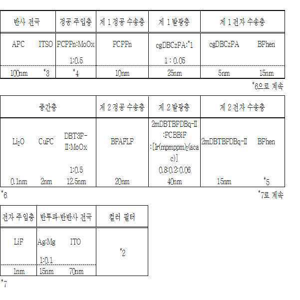
*1
발광 소자 1 내지 3: 1,6BnfAPrn-03 * 1
비교 발광 소자 1 내지 3: 1,6mMemFLPAPrn
Comparative
*2
발광 소자 1 및 비교 발광 소자 1: 0.8μm * 2
발광 소자 2 및 비교 발광 소자 2: 청색 0.8μm
발광 소자 3: 녹색 1.3μm, 비교 발광 소자 3: 적색 2.4μm Light emitting element 3: Green 1.3 µm, Comparative light emitting element 3: Red 2.4 µm
*3 발광 소자 1: 30nm, 발광 소자 2: 80nm, 발광 소자 3: 30nm * 3 Light-emitting element 1: 30 nm, Light-emitting element 2: 80 nm, Light-emitting element 3: 30 nm
비교 발광 소자 1: 30nm, 비교 발광 소자 2: 60nm, 비교 발광 소자 3: 60nm Comparative light emitting device 1: 30 nm, Comparative light emitting device 2: 60 nm, Comparative light emitting device 3: 60 nm
*4 발광 소자 1: 60nm, 발광 소자 2: 47.5nm, 발광 소자 3: 40nm * 4 Light emitting element 1: 60 nm, Light emitting element 2: 47.5 nm, Light emitting element 3: 40 nm
비교 발광 소자 1: 55nm, 비교 발광 소자 2: 70nm, 비교 발광 소자 3: 45nm Comparative light emitting device 1: 55 nm, Comparative light emitting device 2: 70 nm, Comparative light emitting device 3: 45 nm
*5
발광 소자 1 내지 3: 20nm * 5
비교 발광 소자 1 내지 3: 15nm
Comparative
발광 소자 1 내지 3 및 비교 발광 소자 1 내지 3은 각각, 대기에 노출되지 않도록, 질소 분위기를 함유하는 글로브 박스에서 유리 기판을 사용하여 밀봉하였다(구체적으로는, 소자를 둘러싸도록 밀봉 재료를 도포하고, 밀봉 시에 UV 처리(자외광 365nm, 6J/cm2)를 행하고 80℃에서 1시간 가열 처리를 행하였다). 그리고, 이들 발광 소자의 초기 특성을 측정하였다. 또한, 측정은 실온(25℃로 유지된 분위기)에서 행하였다.Light-emitting
도 16은 발광 소자 1 내지 3의 휘도-전류 밀도 특성을 나타낸 것이고, 도 17은 그 전류 효율-휘도 특성을 나타낸 것이고, 도 18은 그 휘도-전압 특성을 나타낸 것이고, 도 19는 그 전류-전압 특성을 나타낸 것이고, 도 20은 그 색도 좌표를 나타낸 것이다.
Fig. 16 shows the luminance-current density characteristics of the
도 21은 비교 발광 소자 1 내지 3의 휘도-전류 밀도 특성을 나타낸 것이고, 도 22는 그 전류 효율-휘도 특성을 나타낸 것이고, 도 23은 그 휘도-전압 특성을 나타낸 것이고, 도 24는 그 전류-전압 특성을 나타낸 것이고, 도 25는 그 색도 좌표를 나타낸 것이다.
21 shows the luminance-current density characteristics of Comparative Light-Emitting
도 20 및 도 25에서와 같이, 1,6BnfAPrn-03을 포함하는 발광 소자 2는 1000cd/m2 부근에서 색도 좌표가 (x, y)=(0.152, 0.037)이고, 1,6mMemFLPAPrn을 포함하는 비교 발광 소자 2는 색도 좌표가 (x, y)=(0.160, 0.087)이다. 이는 발광 소자 2가 비교 발광 소자 2보다 더 깊은 청색 발광을 나타내는 것을 나타낸다.As shown in FIGS. 20 and 25 , the
도 26은 1,6BnfAPrn-03의 톨루엔 용액에서의 1,6BnfAPrn-03의 발광 스펙트럼을 나타낸 것이다. 도 26으로부터 볼 수 있듯이, 톨루엔 용액에서의 1,6BnfAPrn-03의 발광 스펙트럼의 피크 파장은 450nm였다. 발광 스펙트럼의 반치폭은 40nm였다. 한편, 비교 발광 소자에 사용한 톨루엔 용액에서의 1,6mMemFLPAPrn의 피크 파장은 461nm였다. 26 shows the emission spectrum of 1,6BnfAPrn-03 in toluene solution of 1,6BnfAPrn-03. As can be seen from FIG. 26, the peak wavelength of the emission spectrum of 1,6BnfAPrn-03 in toluene solution was 450 nm. The half width of the emission spectrum was 40 nm. On the other hand, the peak wavelength of 1,6mMemFLPAPrn in the toluene solution used for the comparative light emitting element was 461 nm.
다음에, 색도 약 D65의 백색의 광을 얻을 때의, 발광 소자를 포함하는 발광 장치의 소비전력을 계산하였다. 발광 장치의 소비전력은 다음 조건하에서 계산하였다. Next, the power consumption of the light emitting device including the light emitting element when obtaining white light having a chromaticity of about D65 was calculated. The power consumption of the light emitting device was calculated under the following conditions.
[표 2][Table 2]

표 3은 본 실시예의 발광 장치의 계산 결과를 나타낸 것이고, 표 4는 비교예의 발광 장치의 계산 결과를 나타낸 것이다. Table 3 shows the calculation results of the light emitting device of this example, and Table 4 shows the calculation results of the light emitting device of the comparative example.
[표 3][Table 3]

[표 4][Table 4]

상술한 계산 결과에서, 실효 휘도는 진성 휘도×개구율×1/4(각 부화소의 면적비(발광 장치에서 하나의 화소가 적색, 녹색, 청색, 및 황색의 4개의 부화소를 포함한다고 가정))의 계산으로부터 얻었고; 전류량은 전류 밀도×패널 면적×개구율×1/4(각 부화소의 면적비)의 계산으로부터 얻었고; 표시부의 소비전력은 전류량×전압의 계산으로부터 얻었다. In the above calculation result, the effective luminance is the intrinsic luminance x the aperture ratio x 1/4 (area ratio of each sub-pixel (assuming that one pixel in the light emitting device includes four sub-pixels of red, green, blue, and yellow)) was obtained from the calculation of ; The amount of current was obtained from the calculation of current density x panel area x aperture ratio x 1/4 (area ratio of each sub-pixel); The power consumption of the display part was obtained from the calculation of the amount of current x voltage.
표 3 및 표 4로부터 볼 수 있듯이, 본 실시예의 발광 장치의 색도 약 D65의 백색의 광을 얻기 위하여 필요한 청색 발광의 휘도(발광 소자 2의 발광)는 15cd/m2로 낮지만, 비교예의 발광 장치의 색도 약 D65의 백색의 광을 얻기 위하여 필요한 청색 발광의 휘도(비교 발광 소자 2의 발광)는 38cd/m2였다. 이는 실시형태 1 및 실시형태 2에 기재된 바와 같은 형광 물질인 l,6BnfAPrn-03을 청색 발광 재료로서 사용함으로써 청색 발광의 색도가 향상되어, 백색의 광에 필요한 청색 발광의 실효 휘도가 저감되었기 때문이다. 따라서, 백색의 광을 얻기 위하여 필요한 발광 소자 2의 소비전력이 현저히 저감되었다.As can be seen from Tables 3 and 4, the luminance of blue light emission required to obtain white light having a chromaticity of about D65 of the light emitting device of the present Example (light emission of light emitting element 2) is as low as 15 cd/m 2 , but the light emission of Comparative Example The luminance of blue light emission required to obtain white light having a chromaticity of about D65 of the device (light emission of the comparative light-emitting element 2) was 38 cd/m 2 . This is because by using 1,6BnfAPrn-03, which is a fluorescent substance as described in
색도 약 D65의 백색의 광을 얻기 위하여 필요한 발광 소자 3의 소비전력은 22.7mW로 낮지만, 색도 약 D65의 백색의 광을 얻기 위하여 필요한 비교 발광 소자 3의 소비전력은 39.1mW였다. 이 또한 본 실시예의 발광 장치의 소비전력이 더 낮은 것을 나타낸다. The power consumption of the light emitting element 3 required to obtain white light with a chromaticity of about D65 was as low as 22.7 mW, but the power consumption of the comparative light emitting element 3 required to obtain white light with a chromaticity of about D65 was 39.1 mW. This also indicates that the power consumption of the light emitting device of this embodiment is lower.
이 이유는 다음과 같다: 발광 소자 2로부터 깊은 청색 발광이 얻어지기 때문에 발광 소자 1의 청색 발광과 황색 발광의 합성에 의하여 얻어지는 발광색이 달라지고, 색도 약 D65의 백색의 광을 얻기 위하여 필요한 제 3 발광색이 달라졌다. 본 실시예의 발광 장치에서, 제 3 발광으로서 녹색 발광이 필요하였다. 한편, 비교예의 발광 장치에서는 제 3 발광으로서 적색 발광이 필요하였다. 본 실시예의 발광 장치의 백색의 광을 얻기 위하여 필요한 녹색 발광의 휘도의 비율은 비교예의 발광 장치의 백색의 광을 얻기 위하여 필요한 적색 발광의 휘도의 비율보다 높다.
The reason for this is as follows: since deep blue light emission is obtained from light emitting
그러나, 녹색 발광의 시감도는 적색 발광보다 높기 때문에, 녹색 발광을 나타내는 발광 소자 3의 전류 효율은 적색 발광을 나타내는 비교 발광 소자 3의 약 2배 높다. 그러므로, 본 실시예의 발광 장치에서는 백색의 광을 얻기 위하여 필요한 제 3 발광(발광 소자 3의 발광)의 휘도의 비율이 높아진 경우에도, 발광 소자 3의 소비전력을 비교 발광 소자 3보다 낮게 할 수 있다. However, since the visibility of green light emission is higher than that of red light emission, the current efficiency of light emitting element 3 exhibiting green light emission is about twice that of comparative light emission element 3 exhibiting red light emission. Therefore, in the light emitting device of this embodiment, even when the ratio of the luminance of the third light emission (light emission of the light emitting element 3) necessary to obtain white light is increased, the power consumption of the light emitting element 3 can be made lower than that of the comparative light emitting element 3 .
본 실시예의 발광 소자에서, 색도 약 D65의 백색의 광을 휘도 300cd/m2로 얻기 위하여 필요한 발광 소자 2(청색)의 실효 휘도 및 발광 소자 3(녹색)의 실효 휘도는 각각, 비교예의 발광 소자에서 색도 약 D65의 백색의 광을 휘도 300cd/m2로 얻기 위하여 필요한 비교 발광 소자 2(청색)의 실효 휘도 및 비교 발광 소자 3(적색)의 실효 휘도보다 낮지만, 이 부족분은 발광 소자 1의 황색 발광의 높은 휘도에 의하여 보완될 수 있다. 황색 발광을 나타내는 발광 소자 1의 전류 효율은 현저히 높기 때문에, 필요한 휘도의 증가로 인한 소비전력의 증대는 발광 소자 2 및 발광 소자 3에 필요한 휘도의 저하에 의하여 상쇄될 수 있다. 결과적으로, 본 실시예의 발광 장치의 소비전력의 저감이 실현될 수 있다.In the light emitting device of this embodiment, the effective luminance of the light emitting device 2 (blue) and the effective luminance of the light emitting device 3 (green) required to obtain white light having a chromaticity of about D65 at a luminance of 300 cd/m 2 are, respectively, the light emitting device of the comparative example Although the effective luminance of comparative light emitting element 2 (blue) and the effective luminance of comparative light emitting element 3 (red) required to obtain white light with a chromaticity of about D65 at a luminance of 300 cd/m 2 , this deficiency is lower than that of light emitting
그 결과, 백색 표시를 행하는 본 실시예의 발광 장치의, 구동 FET의 소비전력을 제외한 소비전력은 5.8mW/cm2이고, 구동 FET의 소비전력을 포함한 소비전력은 14mW/cm2였다. 백색 표시를 행하는 비교예의 발광 장치의, 구동 FET의 소비전력을 제외한 소비전력은 7.1mW/cm2이고, 구동 FET의 소비전력을 포함한 소비전력은 16mW/cm2였기 때문에, 본 실시예의 발광 장치의 소비전력은 비교예의 소비전력보다 약 10% 내지 20% 낮게 할 수 있다. 또한, 구동 FET를 포함한 발광 장치의 소비전력은 애노드와 캐소드 간의 전압(발광 소자 및 구동 FET 부분들의 전압의 합)이 15V인 것으로 하여 추산하였다.As a result, in the light emitting device of this embodiment performing white display, the power consumption excluding the power consumption of the driving FET was 5.8 mW/cm 2 , and the power consumption including the power consumption of the driving FET was 14 mW/cm 2 . In the light emitting device of the comparative example performing white display, the power consumption excluding the power consumption of the driving FET was 7.1 mW/cm 2 , and the power consumption including the power consumption of the driving FET was 16 mW/cm 2 . The power consumption may be about 10% to 20% lower than the power consumption of the comparative example. In addition, the power consumption of the light emitting device including the driving FET was estimated on the assumption that the voltage between the anode and the cathode (the sum of the voltages of the light emitting element and the driving FET parts) was 15V.
청색 발광 소자는 다른 색의 발광 소자보다 훨씬 높은 전력을 소비하기 때문에 색도의 변화에 의한 소비전력의 저감 효과가 상당하다. 또한, 색도 약 D65의 백색의 광을 얻기 위한 발광색과 휘도의 비율에 관한 밸런스의 변화에 의하여 소비전력의 저감이 실현될 수 있다. 그 결과, 실시형태 1에 기재된 바와 같은 형광 물질을 포함하는 본 실시예의 발광 장치의 소비전력을 낮게 할 수 있다.
Since the blue light emitting device consumes much higher power than other color light emitting devices, the effect of reducing power consumption due to the change in chromaticity is significant. Further, reduction in power consumption can be realized by changing the balance regarding the ratio of luminance and emission color to obtain white light having a chromaticity of about D65. As a result, the power consumption of the light emitting device of this embodiment containing the fluorescent substance as described in
(실시예 2)(Example 2)
본 실시예에서는 백색 표시를 행하는 발광 장치의 소비전력을 계산한 결과에 대하여 설명한다. 본 발명의 발광 장치에는, 발광 소자(적색 발광 소자: 발광 소자 4, 황색 발광 소자: 발광 소자 5, 녹색 발광 소자: 발광 소자 6, 및 청색 발광 소자: 발광 소자 7)를 사용한다. 비교예의 발광 장치에는, 발광 소자(적색 발광 소자: 비교 발광 소자 4, 녹색 발광 소자: 비교 발광 소자 5, 및 청색 발광 소자: 비교 발광 소자 6)를 사용한다.
In this embodiment, the result of calculating the power consumption of the light emitting device performing white display will be described. In the light-emitting device of the present invention, a light-emitting element (red light-emitting element: light-emitting
발광 소자 4 내지 7 및 비교 발광 소자 4 내지 6에 사용한 유기 화합물의 구조식을 이하에 나타내었다.
Structural formulas of the organic compounds used in the light-emitting
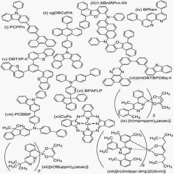
(발광 소자 4 내지 7 및 비교 발광 소자 4 내지 6의 제작 방법)(Method of manufacturing
먼저, 유리 기판 위에 은(Ag), 팔라듐(Pd), 및 구리(Cu)의 합금막(이하에서 이 합금막을 APC라고 함)을 스퍼터링법에 의하여 형성하여 제 1 전극(반사 전극)을 형성하였다. 제 1 전극의 두께는 100nm이고 전극 면적은 2mm×2mm였다. First, an alloy film of silver (Ag), palladium (Pd), and copper (Cu) (hereinafter referred to as APC) was formed on a glass substrate by sputtering to form a first electrode (reflecting electrode). . The thickness of the first electrode was 100 nm and the electrode area was 2 mm x 2 mm.
다음에, 투명 도전막으로서, 제 1 전극 위에 산화 실리콘을 함유하는 인듐 주석 산화물의 막을 스퍼터링법에 의하여 형성하였다. 발광 소자 4(적색)의 투명 도전막의 두께는 80nm이고, 발광 소자 5(황색)의 투명 도전막의 두께는 45nm이고, 발광 소자 6(녹색)의 투명 도전막의 두께는 45nm이고, 발광 소자 7(청색)의 투명 도전막의 두께는 80nm였다. 비교 발광 소자 4(적색)의 투명 도전막의 두께는 85nm이고, 비교 발광 소자 5(녹색)의 투명 도전막의 두께는 45nm이고, 비교 발광 소자 6(청색)의 투명 도전막의 두께는 110nm였다. Next, as a transparent conductive film, a film of indium tin oxide containing silicon oxide was formed on the first electrode by sputtering. The thickness of the transparent conductive film of the light emitting element 4 (red) is 80 nm, the thickness of the transparent conductive film of the light emitting element 5 (yellow) is 45 nm, the thickness of the transparent conductive film of the light emitting element 6 (green) is 45 nm, and the light emitting element 7 (blue) is ), the thickness of the transparent conductive film was 80 nm. The thickness of the transparent conductive film of the comparative light emitting element 4 (red) was 85 nm, the thickness of the transparent conductive film of the comparative light emitting element 5 (green) was 45 nm, and the thickness of the transparent conductive film of the comparative light emitting element 6 (blue) was 110 nm.
그리고, 유기 화합물층의 증착의 전처리로서, 반사 전극 및 투명 도전막이 제공된 기판의 표면을 물로 세정하고, 200℃에서 1시간 베이킹을 행한 다음, 370초 동안 UV 오존 처리를 행하였다. Then, as a pretreatment for deposition of the organic compound layer, the surface of the substrate provided with the reflective electrode and the transparent conductive film was washed with water, baked at 200° C. for 1 hour, and then subjected to UV ozone treatment for 370 seconds.
그 후, 압력이 약 10-4Pa로 감압된 진공 증착 장치로 기판을 옮겨서 진공 증착 장치의 가열 체임버에서 170℃에서 30분 동안 진공 베이킹을 행한 다음, 기판을 30분 동안 냉각시켰다.Thereafter, the substrate was transferred to a vacuum deposition apparatus in which the pressure was reduced to about 10 −4 Pa, and vacuum baking was performed at 170° C. for 30 minutes in a heating chamber of the vacuum deposition apparatus, and then the substrate was cooled for 30 minutes.
그리고, 투명 도전막이 형성된 면이 아래쪽을 향하도록, 기판을 진공 증착 장치에 제공된 기판 홀더에 고정시켰다. 진공 증착 장치의 압력을 약 10-4Pa로 감압하였다. 그 후, 투명 도전막 상에, 저항 가열을 사용한 공증착에 의하여, 구조식(i)으로 표기되는 3-[4-(9-페난트릴)-페닐]-9-페닐-9H-카바졸(약칭: PCPPn) 및 산화 몰리브데넘(VI)을 퇴적함으로써 제 1 정공 주입층을 형성하였다. 발광 소자 4(적색)의 제 1 정공 주입층의 두께는 30nm이고, 발광 소자 5(황색)의 제 1 정공 주입층의 두께는 40nm이고, 발광 소자 6(녹색)의 제 1 정공 주입층의 두께는 22.5nm이고, 발광 소자 7(청색)의 제 1 정공 주입층의 두께는 50nm였다. 비교 발광 소자 4(적색)의 제 1 정공 주입층의 두께는 10nm이고, 비교 발광 소자 5(녹색)의 제 1 정공 주입층의 두께는 10nm이고, 비교 발광 소자 6(청색)의 제 1 정공 주입층의 두께는 15nm였다. 산화 몰리브데넘에 대한 PCPPn의 중량비는 1:0.5로 조정하였다.Then, the substrate was fixed to a substrate holder provided in the vacuum vapor deposition apparatus so that the side on which the transparent conductive film was formed was facing downward. The pressure of the vacuum deposition apparatus was reduced to about 10 -4 Pa. Then, 3-[4-(9-phenanthryl)-phenyl]-9-phenyl- 9H -carbazole ( A first hole injection layer was formed by depositing abbreviation: PCPPn) and molybdenum (VI) oxide. The thickness of the first hole injection layer of the light emitting element 4 (red) is 30 nm, the thickness of the first hole injection layer of the light emitting element 5 (yellow) is 40 nm, and the thickness of the first hole injection layer of the light emitting element 6 (green) is is 22.5 nm, and the thickness of the first hole injection layer of the light emitting element 7 (blue) was 50 nm. The thickness of the first hole injection layer of the comparative light emitting element 4 (red) is 10 nm, the thickness of the first hole injection layer of the comparative light emitting element 5 (green) is 10 nm, and the first hole injection of the comparative light emitting element 6 (blue) is The thickness of the layer was 15 nm. The weight ratio of PCPPn to molybdenum oxide was adjusted to 1:0.5.
다음에, 제 1 정공 주입층 상에 PCPPn을 퇴적하여 제 1 정공 수송층을 형성하였다. 발광 소자 4 내지 7 각각의 제 1 정공 수송층의 두께는 10nm이고, 비교 발광 소자 4 내지 6 각각의 제 1 정공 수송층의 두께는 15nm였다.
Next, PCPPn was deposited on the first hole injection layer to form a first hole transport layer. The thickness of the first hole transport layer of each of the
제 1 정공 수송층 상에, 구조식(ii)으로 표기되는 7-[4-(10-페닐-9-안트릴)페닐]-7H-다이벤조[c,g]카바졸(약칭: cgDBCzPA) 및 구조식(iii)으로 표기되는 N,N'-(피렌-1,6-다이일)비스[(6,N-다이페닐벤조[b]나프토[1,2-d]퓨란)-8-아민](약칭: 1,6BnfAPrn-03)을, 1,6BnfAPrn-03에 대한 cgDBCzPA의 중량비가 1:0.05가 되도록 두께 25nm로 퇴적함으로써 제 1 발광층을 형성하였다.On the first hole transport layer, 7-[4-(10-phenyl-9-anthryl)phenyl]-7H-dibenzo[ c , g ]carbazole (abbreviation: cgDBCzPA ) represented by the structural formula (ii) and N , N '-(pyrene-1,6-diyl)bis[(6, N -diphenylbenzo[ b ]naphtho[1,2- d ]furan)-8-amine represented by the structural formula (iii) ] (abbreviation: 1,6BnfAPrn-03) was deposited to a thickness of 25 nm so that the weight ratio of cgDBCzPA to 1,6BnfAPrn-03 was 1:0.05 to form a first light emitting layer.
그리고, cgDBCzPA를 두께 5nm로 퇴적하고, 구조식(iv)으로 표기되는 바소페난트롤린(약칭: BPhen)을 두께 15nm로 퇴적하는 식으로, 제 1 발광층 위에 제 1 전자 수송층을 형성하였다. Then, a first electron transport layer was formed on the first light emitting layer by depositing cgDBCzPA to a thickness of 5 nm and depositing vasophenanthroline (abbreviation: BPhen) represented by the structural formula (iv) to a thickness of 15 nm.
제 1 전자 수송층을 형성한 후, 산화 리튬(Li2O)을 두께 0.1nm로 증착하였다. 그리고, 구조식(xi)으로 표기되는 구리 프탈로사이아닌(약칭: CuPc)을 두께 2nm로 증착하였다. 그 후, 구조식(v)으로 표기되는 4,4',4''-(벤젠-1,3,5-트라이일)트라이(다이벤조싸이오펜)(약칭: DBT3P-II) 및 산화 몰리브데넘을, 산화 몰리브데넘에 대한 DBT3P-II의 중량비가 1:0.5가 되도록 공증착하였다. 이와 같이 하여 중간층을 형성하였다. 중간층의 두께는 12.5nm였다.After forming the first electron transport layer, lithium oxide (Li 2 O) was deposited to a thickness of 0.1 nm. Then, copper phthalocyanine (abbreviation: CuPc) represented by the structural formula (xi) was deposited to a thickness of 2 nm. Then, 4,4',4''-(benzene-1,3,5-triyl)tri(dibenzothiophene) (abbreviation: DBT3P-II) represented by the structural formula (v) and molybdate oxide It was co-deposited so that the weight ratio of DBT3P-II to molybdenum oxide was 1:0.5. In this way, an intermediate layer was formed. The thickness of the intermediate layer was 12.5 nm.
다음에, 중간층 상에, 구조식(vi)으로 표기되는 4-페닐-4'-(9-페닐플루오렌-9-일)트라이페닐아민(약칭: BPAFLP)을 두께 20nm로 증착함으로써 제 2 정공 수송층을 형성하였다. Next, on the intermediate layer, 4-phenyl-4'-(9-phenylfluoren-9-yl)triphenylamine (abbreviation: BPAFLP) represented by the structural formula (vi) was deposited to a thickness of 20 nm to form a second hole transport layer was formed.
발광 소자 4 내지 7 각각에 대해서는, 제 2 정공 수송층을 형성한 후, 구조식(vii)으로 표기되는 2-[3'-(다이벤조싸이오펜-4-일)바이페닐-3-일]다이벤조[f,h]퀴녹살린(약칭: 2mDBTBPDBq-II), 구조식(viii)으로 표기되는 N-(1,1'-바이페닐-4-일)-9,9-다이메틸-N-[4-(9-페닐-9H-카바졸-3-일)페닐]-9H-플루오렌-2-아민(약칭: PCBBiF), 및 구조식(ix)으로 표기되는 비스{2-[5-메틸-6-(2-메틸페닐)-4-피리미딘일-κN3]페닐-κC}(2,4-펜테인다이오네이토-κ2 O,O')이리듐(III)(약칭: [Ir(mpmppm)2(acac)])을, PCBBiF 및 [Ir(mpmppm)2(acac)]에 대한 2mDBTBPDBq-II의 중량비가 0.8:0.2:0.06이 되도록 공증착하였다. 이와 같이 하여 제 2 발광층을 형성하였다. 제 2 발광층의 두께는 40nm였다.For each of the
비교 발광 소자 4 내지 6 각각에 대해서는, 제 2 정공 수송층을 형성한 후, 2mDBTBPDBq-II, PCBBiF, 및 구조식(xii)으로 표기되는 비스[2-(6-tert-뷰틸-4-피리미딘일-κN3)페닐-κC](2,4-펜테인다이오네이토-κ2 O,O')이리듐(III)(약칭: [Ir(tBuppm)2(acac)])을 두께 20nm로 공증착하였다. 그 후, 2mDBTBPDBq-II 및 비스{4,6-다이메틸-2-[5-(2,6-다이메틸페닐)-3-(3,5-다이메틸페닐)-2-피라진일-κN]페닐-κC}(2,8-다이메틸-4,6-노네인다이오네이토-κ2 O,O')이리듐(III)(약칭: [Ir(dmdppr-dmp)2(divm)])을, [Ir(dmdppr-dmp)2(divm)]에 대한 2mDBTBPDBq-II의 중량비가 1:0.06이 되도록 두께 20nm로 공증착하였다. 이와 같이 하여 제 2 발광층을 형성하였다.For each of Comparative Light-Emitting
발광 소자 4 내지 7 각각에 대해서는, 제 2 발광층 상에, 2mDBTBPDBq-II를 두께 15nm로 증착하였다. 비교 발광 소자 4 내지 6 각각에 대해서는, 제 2 발광층 상에, 2mDBTBPDBq-II를 두께 30nm로 증착하였다. 발광 소자 4 내지 7 각각에 대해서는, 2mDBTBPDBq-II 상에 BPhen을 두께 20nm로 더 증착하였다. 비교 발광 소자 4 내지 6 각각에 대해서는, 2mDBTBPDBq-II 상에 BPhen을 두께 15nm로 더 증착하였다. 이와 같이 하여 제 2 전자 수송층을 형성하였다.
For each of the light-emitting
그 후, 플루오린화 리튬을 두께 1nm로 증착하여 전자 주입층을 형성하였다. 그리고, 은과 마그네슘을 두께 15nm, 체적비 1:0.1(=은:마그네슘)로 공증착하였다. 다음에, 스퍼터링법에 의하여 ITO를 두께 70nm로 퇴적하였다. 이와 같이 하여 제 2 전극(반투과·반반사 전극)을 형성하였다. 상술한 단계를 거쳐, 발광 소자 4 내지 7 및 비교 발광 소자 4 내지 6을 제작하였다. 또한, 상술한 모든 증착 단계에서, 증착은 저항 가열법에 의하여 행하였다.
Thereafter, lithium fluoride was deposited to a thickness of 1 nm to form an electron injection layer. Then, silver and magnesium were co-deposited with a thickness of 15 nm and a volume ratio of 1:0.1 (=silver:magnesium). Next, ITO was deposited to a thickness of 70 nm by sputtering. In this way, the second electrode (semi-transmissive/semi-reflective electrode) was formed. Through the above-described steps, light emitting
발광 소자 4 내지 7 및 비교 발광 소자 4 내지 6의 소자 구조를 이하에 열거하였다.
The device structures of the light-emitting
[표 5][Table 5]

*10 발광 소자 4: 80nm, 발광 소자 5: 45nm, 발광 소자 6: 45nm, 발광 소자 7: 80nm * 10 Light emitting element 4: 80 nm, Light emitting element 5: 45 nm, Light emitting element 6: 45 nm, Light emitting element 7: 80 nm
비교 발광 소자 4: 85nm, 비교 발광 소자 5: 45nm, 비교 발광 소자 6: 110nm Comparative light emitting element 4: 85 nm, Comparative light emitting element 5: 45 nm, Comparative light emitting element 6: 110 nm
*11 발광 소자 4: 30nm, 발광 소자 5: 40nm, 발광 소자 6: 22.5nm, 발광 소자 7: 50nm * 11 Light emitting element 4: 30 nm, Light emitting element 5: 40 nm, Light emitting element 6: 22.5 nm, Light emitting element 7: 50 nm
비교 발광 소자 4 : 10nm, 비교 발광 소자 5: 10nm, 비교 발광 소자 6: 15nm Comparative light emitting element 4: 10 nm, Comparative light emitting element 5: 10 nm, Comparative light emitting element 6: 15 nm
*12
발광 소자 4 내지 7: 10nm, 비교 발광 소자 4 내지 6: 15nm * 12
*13
발광 소자 4 내지 7 * 13
2mDBTBPDBq-II:PCBBiF:[Ir(mpmppm)2(acac)]=0.8:0.2:0.06, 40nm2mDBTBPDBq-II:PCBBiF:[Ir(mpmppm) 2 (acac)]=0.8:0.2:0.06, 40nm
비교 발광 소자 4 내지 6
Comparative
2mDBTBPDBq-II:PCBBiF:[Ir(tBuppm)2(acac)]=0.7:0.3:0.06, 20nm2mDBTBPDBq-II:PCBBiF:[Ir(tBuppm) 2 (acac)]=0.7:0.3:0.06, 20nm
+2mDBTBPDBq-II:[Ir(dmdppr-dmp)2(divm)]=1:0.06, 20nm+2mDBTBPDBq-II:[Ir(dmdppr-dmp) 2 (divm)]=1:0.06, 20nm
*14
발광 소자 4 내지 7: 15nm, 비교 발광 소자 4 내지 6: 30nm * 14
*15
발광 소자 4 내지 7: 20nm, 비교 발광 소자 4 내지 6: 15nm * 15 light emitting
*16
발광 소자 4 및 비교 발광 소자 4: 적색 2.4μm * 16
발광 소자 5: 황색 0.8μm Light emitting element 5: yellow 0.8 μm
발광 소자 6 및 비교 발광 소자 5: 녹색 1.3μm
발광 소자 7 및 비교 발광 소자 6: 청색 0.8μm Light emitting element 7 and comparative light emitting element 6: blue 0.8 μm
발광 소자 4 내지 7 및 비교 발광 소자 4 내지 6은 각각, 대기에 노출되지 않도록, 질소 분위기를 함유하는 글로브 박스에서 유리 기판을 사용하여 밀봉하였다(구체적으로는, 소자를 둘러싸도록 밀봉 재료를 도포하고, 밀봉 시에 UV 처리(자외광 365nm, 6J/cm2)를 행하고 80℃에서 1시간 가열 처리를 행하였다). 그리고, 이들 발광 소자의 초기 특성을 측정하였다. 또한, 측정은 실온(25℃로 유지된 분위기)에서 행하였다.Light-emitting
도 28은 발광 소자 4 내지 7의 휘도-전류 밀도 특성을 나타낸 것이고, 도 29는 그 전류 효율-휘도 특성을 나타낸 것이고, 도 30은 그 휘도-전압 특성을 나타낸 것이고, 도 31은 그 전류-전압 특성을 나타낸 것이고, 도 32는 그 색도 좌표를 나타낸 것이다.
Fig. 28 shows the luminance-current density characteristics of the
도 33은 비교 발광 소자 4 내지 6의 휘도-전류 밀도 특성을 나타낸 것이고, 도 34는 그 전류 효율-휘도 특성을 나타낸 것이고, 도 35는 그 휘도-전압 특성을 나타낸 것이고, 도 36은 그 전류-전압 특성을 나타낸 것이다.
33 shows the luminance-current density characteristics of comparative
다음에, 발광 소자를 포함하는 발광 장치의, 색도 약 D65의 백색의 광을 얻기 위한 소비전력을 계산하였다. 발광 장치의 소비전력은 다음 조건하에서 계산하였다. Next, the power consumption for obtaining white light with a chromaticity of about D65 of the light emitting device including the light emitting element was calculated. The power consumption of the light emitting device was calculated under the following conditions.
[표 6][Table 6]
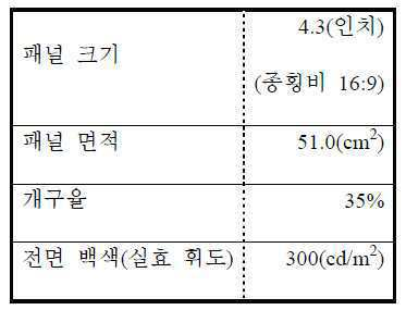
표 7은 본 실시예의 발광 장치의 계산 결과를 나타낸 것이고, 표 8은 비교예의 발광 장치의 계산 결과를 나타낸 것이다. Table 7 shows the calculation results of the light emitting device of this example, and Table 8 shows the calculation results of the light emitting device of the comparative example.
[표 7][Table 7]

[표 8][Table 8]

상술한 계산 결과에서, 실효 휘도는 진성 휘도×개구율×1/4(각 부화소의 면적비(발광 장치에서 하나의 화소가 적색, 녹색, 청색, 및 황색의 4개의 부화소를 포함한다고 가정))의 계산으로부터 얻었고; 전류량은 전류 밀도×패널 면적×개구율×1/4(각 부화소의 면적비)의 계산으로부터 얻었고; 표시부의 소비전력은 전류량×전압의 계산으로부터 얻었다. In the above calculation result, the effective luminance is the intrinsic luminance x the aperture ratio x 1/4 (area ratio of each sub-pixel (assuming that one pixel in the light emitting device includes four sub-pixels of red, green, blue, and yellow)) was obtained from the calculation of ; The amount of current was obtained from the calculation of current density x panel area x aperture ratio x 1/4 (area ratio of each sub-pixel); The power consumption of the display part was obtained from the calculation of the amount of current x voltage.
표 7 및 표 8로부터 볼 수 있듯이, 본 실시예의 발광 장치의 백색의 광을 얻기 위한 소비전력은 266mW이고, 비교예의 발광 장치의 백색의 광을 얻기 위한 소비전력은 394mW였기 때문에, 본 실시예의 발광 장치는 비교예보다 전력을 적게 소비한다. 비교예의 발광 장치에서는, 백색의 광을 방출할 때에 비교 발광 소자 4(적색)와 비교 발광 소자 5(녹색)의 양쪽이 일정한 비율의 진성 휘도를 필요로 한다. 한편, 본 실시예의 발광 장치에서는, 백색의 광을 방출할 때에 발광 소자 4(적색)가 광을 방출하지 않고 발광 소자 6(녹색)의 발광 휘도가 139cd/m2로 낮기 때문에, 이들이 실질적으로 소비전력에 영향을 미치지 않는다. 즉, 본 실시예의 발광 장치에서는, 백색 발광을 나타낼 때에 실질적으로 발광 소자 7(청색) 및 발광 소자 5(황색)만이 광을 방출한다. 본 실시예와 비교예의 발광 장치들의 청색 발광 소자의 소비전력은 실질적으로 동일하지만, 발광 소자 5(황색)의 전류 효율이 137cd/A로 높기 때문에, 본 실시예의 발광 장치의 소비전력은 비교예의 발광 장치보다 현저히 낮았다.As can be seen from Tables 7 and 8, the power consumption for obtaining white light of the light emitting device of this example was 266 mW, and the power consumption for obtaining white light of the light emitting device of Comparative Example was 394 mW. The device consumes less power than the comparative example. In the light emitting device of the comparative example, both the comparative light emitting element 4 (red) and the comparative light emitting element 5 (green) require a constant ratio of intrinsic luminance when emitting white light. On the other hand, in the light emitting device of this embodiment, when emitting white light, light emitting element 4 (red) does not emit light and light emitting luminance of light emitting element 6 (green) is as low as 139 cd/m 2 , so they are consumed substantially. Does not affect power. That is, in the light emitting device of this embodiment, substantially only light emitting element 7 (blue) and light emitting element 5 (yellow) emit light when white light is emitted. Although the power consumption of the blue light emitting device of the light emitting devices of this embodiment and the comparative example is substantially the same, since the current efficiency of the light emitting device 5 (yellow) is as high as 137 cd/A, the power consumption of the light emitting device of this example is the same as that of the light emitting device of the comparative example. significantly lower than the device.
(실시예 3)(Example 3)
본 발명의 일 형태에 따른 발광 장치가 색도 약 D65의 백색 표시를 휘도 300cd/m2로 행하는 경우의 휘도 열화의 추정 결과를 나타낸다. 본 실시예에서는, 전류 밀도가 일정한 조건하에서, 본 발명의 일 형태에 따른 발광 장치의 발광 소자와 동일한 구조를 가지는 발광 소자 8(청색)과 발광 소자 9(황색)의 구동 테스트를 행하였다. 발광 소자 8의 초기 휘도는 300cd/m2로 설정하고, 발광 소자 9의 초기 휘도는 3000cd/m2로 설정하였다. 이들 값은 다음 조건으로 본 발명의 일 형태에 따른 발광 장치에서 색도 약 D65의 백색 표시를 행하기 위하여 필요한 휘도값에 가깝다. 백색 표시를 행하는 것으로 가정하여 구동 테스트를 행한 이유는, 백색 표시를 위해서는 연속적으로 발광을 행할 필요가 있고, 이에 따라 소자는 백색 표시를 행할 때에 가장 빨리 열화되기 때문이다.The estimation result of luminance deterioration when the light emitting device according to one embodiment of the present invention performs white display with a chromaticity of about D65 at a luminance of 300 cd/m 2 is shown. In this embodiment, under the condition that the current density is constant, the driving tests of the light emitting element 8 (blue) and the light emitting element 9 (yellow) having the same structure as the light emitting element of the light emitting device according to one embodiment of the present invention were conducted. The initial luminance of the
[표 9][Table 9]

또한, 광은 황색 발광층으로부터 추출되기 때문에 적색 발광 소자 또는 녹색 발광 소자는 황색 발광 소자와 비슷한 열화 거동을 나타낼 것으로 생각되고, 또한 색도 약 D65의 백색 표시를 행할 때에 필요한 적색 발광 소자 및 녹색 발광 소자의 휘도는 실시예 2에 기재된 바와 같이 낮아, 이들은 신뢰성에 영향을 미치지 않기 때문에, 적색 발광 소자 또는 녹색 발광 소자에는 구동 테스트를 행하지 않았다. In addition, since light is extracted from the yellow light emitting layer, it is considered that a red light emitting element or a green light emitting element exhibits similar degradation behavior to that of a yellow light emitting element, and the red light emitting element and green light emitting element required for white display with a chromaticity of about D65. The luminance is low as described in Example 2, and since they do not affect reliability, no driving test was performed on the red light emitting element or the green light emitting element.
발광 소자 8 및 9에 사용한 유기 화합물의 구조식을 이하에 나타내었다.
The structural formulas of the organic compounds used for the light-emitting

(발광 소자 8 및 9의 제작 방법)(Method of manufacturing
먼저, 유리 기판 위에 은(Ag), 팔라듐(Pd), 및 구리(Cu)의 합금막(이하에서 이 합금막을 APC라고 함)을 스퍼터링법에 의하여 형성하여 제 1 전극(반사 전극)을 형성하였다. 제 1 전극의 두께는 100nm이고 전극 면적은 2mm×2mm였다. First, an alloy film of silver (Ag), palladium (Pd), and copper (Cu) (hereinafter referred to as APC) was formed on a glass substrate by sputtering to form a first electrode (reflecting electrode). . The thickness of the first electrode was 100 nm and the electrode area was 2 mm x 2 mm.
다음에, 투명 도전막으로서, 제 1 전극 위에 산화 실리콘을 함유하는 인듐 주석 산화물의 막을 스퍼터링법에 의하여 형성하였다. 발광 소자 8(청색)의 투명 도전막의 두께는 85nm이고, 발광 소자 9(황색)의 투명 도전막의 두께는 65nm였다. Next, as a transparent conductive film, a film of indium tin oxide containing silicon oxide was formed on the first electrode by sputtering. The thickness of the transparent conductive film of the light emitting element 8 (blue) was 85 nm, and the thickness of the transparent conductive film of the light emitting element 9 (yellow) was 65 nm.
그리고, 유기 화합물층의 증착의 전처리로서, 반사 전극 및 투명 도전막이 제공된 기판의 표면을 물로 세정하고, 200℃에서 1시간 베이킹을 행한 다음, 370초 동안 UV 오존 처리를 행하였다. Then, as a pretreatment for deposition of the organic compound layer, the surface of the substrate provided with the reflective electrode and the transparent conductive film was washed with water, baked at 200° C. for 1 hour, and then subjected to UV ozone treatment for 370 seconds.
그 후, 압력이 약 10-4Pa로 감압된 진공 증착 장치로 기판을 옮겨서 진공 증착 장치의 가열 체임버에서 170℃에서 30분 동안 진공 베이킹을 행한 다음, 기판을 30분 동안 냉각시켰다.Thereafter, the substrate was transferred to a vacuum deposition apparatus in which the pressure was reduced to about 10 −4 Pa, and vacuum baking was performed at 170° C. for 30 minutes in a heating chamber of the vacuum deposition apparatus, and then the substrate was cooled for 30 minutes.
그리고, 투명 도전막이 형성된 면이 아래쪽을 향하도록, 기판을 진공 증착 장치에 제공된 기판 홀더에 고정시켰다. 그 후, 투명 도전막 상에, 저항 가열을 사용한 공증착에 의하여, 구조식(xiv)으로 표기되는 9-페닐-3-[4-(10-페닐-9-안트릴)페닐]-9H-카바졸(약칭: PCzPA) 및 산화 몰리브데넘(VI)을 퇴적함으로써 제 1 정공 주입층을 형성하였다. 발광 소자 8(청색)의 제 1 정공 주입층의 두께는 40nm이고, 발광 소자 9(황색)의 제 1 정공 주입층의 두께는 45nm였다. 산화 몰리브데넘에 대한 PCzPA의 중량비는 1:0.5로 조정하였다.Then, the substrate was fixed to a substrate holder provided in the vacuum vapor deposition apparatus so that the side on which the transparent conductive film was formed was facing downward. Then, on the transparent conductive film, 9-phenyl-3-[4-(10-phenyl-9-anthryl)phenyl] -9H- represented by the structural formula (xiv) by co-evaporation using resistance heating. A first hole injection layer was formed by depositing carbazole (abbreviated: PCzPA) and molybdenum (VI) oxide. The thickness of the first hole injection layer of the light emitting element 8 (blue) was 40 nm, and the thickness of the first hole injection layer of the light emitting element 9 (yellow) was 45 nm. The weight ratio of PCzPA to molybdenum oxide was adjusted to 1:0.5.
다음에, 제 1 정공 주입층 상에 PCzPA를 퇴적하여 제 1 정공 수송층을 형성하였다. 제 1 정공 수송층의 두께는 20nm였다. Next, PCzPA was deposited on the first hole injection layer to form a first hole transport layer. The thickness of the first hole transport layer was 20 nm.
제 1 정공 수송층 상에, 구조식(ii)으로 표기되는 7-[4-(10-페닐-9-안트릴)페닐]-7H-다이벤조[c,g]카바졸(약칭: cgDBCzPA) 및 구조식(iii)으로 표기되는 N,N'-(피렌-1,6-다이일)비스[(6,N-다이페닐벤조[b]나프토[1,2-d]퓨란)-8-아민](약칭: 1,6BnfAPrn-03)을, 1,6BnfAPrn-03에 대한 cgDBCzPA의 중량비가 1:0.03이 되도록 두께 25nm로 퇴적함으로써 제 1 발광층을 형성하였다.On the first hole transport layer, 7-[4-(10-phenyl-9-anthryl)phenyl]-7H-dibenzo[ c , g ]carbazole (abbreviation: cgDBCzPA ) represented by the structural formula (ii) and N , N '-(pyrene-1,6-diyl)bis[(6, N -diphenylbenzo[ b ]naphtho[1,2- d ]furan)-8-amine represented by the structural formula (iii) ] (abbreviation: 1,6BnfAPrn-03) was deposited to a thickness of 25 nm so that the weight ratio of cgDBCzPA to 1,6BnfAPrn-03 was 1:0.03 to form a first light emitting layer.
그리고, cgDBCzPA를 두께 10nm로 퇴적하고, 구조식(vi)으로 표기되는 바소페난트롤린(약칭: BPhen)을 두께 10nm로 퇴적하는 식으로, 제 1 발광층 위에 제 1 전자 수송층을 형성하였다. Then, a first electron transport layer was formed on the first light emitting layer by depositing cgDBCzPA to a thickness of 10 nm and depositing vasophenanthroline (abbreviation: BPhen) represented by the structural formula (vi) to a thickness of 10 nm.
제 1 전자 수송층을 형성한 후, 산화 리튬(Li2O)을 두께 0.1nm로 증착하였다. 그리고, 구조식(xi)으로 표기되는 구리 프탈로사이아닌(약칭: CuPc)을 두께 2nm로 증착하였다. 그 후, PCzPA 및 산화 몰리브데넘을, 산화 몰리브데넘에 대한 PCzPA의 중량비가 1:0.5가 되도록 공증착하였다. 이와 같이 하여 중간층을 형성하였다. 중간층의 두께는 12.5nm였다.After forming the first electron transport layer, lithium oxide (Li 2 O) was deposited to a thickness of 0.1 nm. Then, copper phthalocyanine (abbreviation: CuPc) represented by the structural formula (xi) was deposited to a thickness of 2 nm. Thereafter, PCzPA and molybdenum oxide were co-deposited so that the weight ratio of PCzPA to molybdenum oxide was 1:0.5. In this way, an intermediate layer was formed. The thickness of the intermediate layer was 12.5 nm.
다음에, 중간층 상에, PCzPA를 두께 20nm로 증착함으로써 제 2 정공 수송층을 형성하였다. Next, on the intermediate layer, a second hole transport layer was formed by vapor-depositing PCzPA to a thickness of 20 nm.
제 2 정공 수송층을 형성한 후, 구조식(vii)으로 표기되는 2-[3'-(다이벤조싸이오펜-4-일)바이페닐-3-일]다이벤조[f,h]퀴녹살린(약칭: 2mDBTBPDBq-II), 구조식(viii)으로 표기되는 N-(1,1'-바이페닐-4-일)-9,9-다이메틸-N-[4-(9-페닐-9H-카바졸-3-일)페닐]-9H-플루오렌-2-아민(약칭: PCBBiF), 및 구조식(ix)으로 표기되는 비스{2-[5-메틸-6-(2-메틸페닐)-4-피리미딘일-κN3]페닐-κC}(2,4-펜테인다이오네이토-κ2 O,O')이리듐(III)(약칭: [Ir(mpmppm)2(acac)])을, PCBBiF 및 [Ir(mpmppm)2(acac)]에 대한 2mDBTBPDBq-II의 중량비가 0.8:0.2:0.06이 되도록 공증착하였다. 이와 같이 하여 제 2 발광층을 형성하였다. 제 2 발광층의 두께는 40nm였다.After forming the second hole transport layer, 2-[3'-(dibenzothiophen-4-yl)biphenyl-3-yl]dibenzo[ f , h ]quinoxaline (abbreviated as : 2mDBTBPDBq-II), N- (1,1'-biphenyl-4-yl)-9,9-dimethyl- N- [4-(9-phenyl-9H- carba ) represented by the structural formula (viii) zol-3-yl)phenyl]-9H-fluoren-2-amine (abbreviation: PCBBiF ), and bis{2-[5-methyl-6-(2-methylphenyl)-4 represented by the structural formula (ix) -pyrimidinyl-κ N 3]phenyl-κ C } (2,4-pentanedionato-κ 2 O , O ′) iridium (III) (abbreviation: [Ir(mpmppm) 2 (acac)]) was co-deposited so that the weight ratio of 2mDBTBPDBq-II to PCBBiF and [Ir(mpmppm) 2 (acac)] was 0.8:0.2:0.06. In this way, a second light emitting layer was formed. The thickness of the second light emitting layer was 40 nm.
제 2 발광층 상에, 2mDBTBPDBq-II를 두께 15nm로 증착하였다. 2mDBTBPDBq-II 상에, BPhen을 두께 20nm로 증착하였다. 이와 같이 하여 제 2 전자 수송층을 형성하였다. On the second light-emitting layer, 2mDBTBPDBq-II was deposited to a thickness of 15 nm. On 2mDBTBPDBq-II, BPhen was deposited to a thickness of 20 nm. In this way, a second electron transport layer was formed.
그 후, 플루오린화 리튬을 두께 1nm로 증착하여 전자 주입층을 형성하였다. 그리고, 은과 마그네슘을 두께 15nm, 체적비 1:0.1(=은:마그네슘)로 공증착하였다. 다음에, 스퍼터링법에 의하여 ITO를 두께 70nm로 퇴적하였다. 이와 같이 하여 제 2 전극(반투과·반반사 전극)을 형성하였다. 상술한 단계를 거쳐, 발광 소자 8(청색) 및 발광 소자 9(황색)를 제작하였다. 또한, 상술한 모든 증착 단계에서, 증착은 저항 가열법에 의하여 행하였다. Thereafter, lithium fluoride was deposited to a thickness of 1 nm to form an electron injection layer. Then, silver and magnesium were co-deposited with a thickness of 15 nm and a volume ratio of 1:0.1 (=silver:magnesium). Next, ITO was deposited to a thickness of 70 nm by sputtering. In this way, the second electrode (semi-transmissive/semi-reflective electrode) was formed. Through the above-described steps, light emitting device 8 (blue) and light emitting device 9 (yellow) were manufactured. In addition, in all the above-mentioned vapor deposition steps, vapor deposition was performed by the resistance heating method.
발광 소자 8 및 9의 소자 구조를 이하에 열거하였다.
The device structures of light-emitting
[표 10][Table 10]

*19 발광 소자 8: 85nm, 발광 소자 9: 65nm * 19 Light emitting element 8: 85 nm, Light emitting element 9: 65 nm
*20 발광 소자 8: 40nm, 발광 소자 9: 45nm * 20 Light emitting element 8: 40 nm, Light emitting element 9: 45 nm
*21 발광 소자 8: 청색 0.8μm, 발광 소자 9: 황색 0.8μm * 21 Light emitting element 8: blue 0.8 µm, light emitting element 9: yellow 0.8 µm
발광 소자 8(청색) 및 발광 소자 9(황색)는 각각, 대기에 노출되지 않도록, 질소 분위기를 함유하는 글로브 박스에서 유리 기판을 사용하여 밀봉하였다(구체적으로는, 소자를 둘러싸도록 밀봉 재료를 도포하고, 밀봉 시에 UV 처리(자외광 365nm, 6J/cm2)를 행하고 80℃에서 1시간 가열 처리를 행하였다). 그리고, 이들 발광 소자의 초기 특성을 측정하였다. 또한, 측정은 실온(25℃로 유지된 분위기)에서 행하였다. 발광 소자 8에 대해서는, 청색 컬러 필터를 통과하는 광에 대하여 측정을 행하였다. 발광 소자 9에 대해서는, 황색 컬러 필터를 통과하는 광에 대하여 측정을 행하였다.Light-emitting element 8 (blue) and light-emitting element 9 (yellow) were each sealed using a glass substrate in a glove box containing a nitrogen atmosphere so as not to be exposed to the atmosphere (specifically, a sealing material was applied to surround the element) and UV treatment (UV light 365 nm, 6J/cm 2 ) at the time of sealing and heat treatment at 80° C. for 1 hour). Then, the initial characteristics of these light emitting devices were measured. In addition, the measurement was performed at room temperature (atmosphere maintained at 25 degreeC). For the
도 39는 발광 소자 8(청색) 및 발광 소자 9(황색)의 휘도-전류 밀도 특성을 나타낸 것이고, 도 40은 그 전류 효율-휘도 특성을 나타낸 것이고, 도 41은 그 휘도-전압 특성을 나타낸 것이고, 도 42는 그 전류-전압 특성을 나타낸 것이고, 도 43은 그 발광 스펙트럼을 나타낸 것이다. 이들 그래프에 나타낸 바와 같이 발광 소자 8 및 발광 소자 9는 양호한 특성을 가진다.
Fig. 39 shows the luminance-current density characteristics of the light-emitting element 8 (blue) and the light-emitting element 9 (yellow), Fig. 40 shows the current efficiency-luminance characteristic, and Fig. 41 shows the luminance-voltage characteristic. , FIG. 42 shows its current-voltage characteristics, and FIG. 43 shows its emission spectrum. As shown in these graphs, the light-emitting
다음에, 발광 소자 8의 초기 휘도가 300cd/m2이고, 발광 소자 9의 초기 휘도가 3000cd/m2이고, 전류 밀도가 일정한 조건하에서 발광 소자 8(청색) 및 발광 소자 9(황색)의 구동 테스트를 행하였다. 도 44는 초기 휘도를 100%로 하였을 때의 구동 시간에 따른 휘도의 변화를 나타낸 것이다.Next, the light-emitting element 8 (blue) and the light-emitting element 9 (yellow) are driven under the condition that the initial luminance of the light-emitting
도 44에 나타낸 바와 같이, 발광 소자 8의 휘도는 초기 휘도의 90%까지 저하되는 데 약 2300시간이 걸렸고, 발광 소자 9의 휘도는 초기 휘도의 90%까지 저하되는 데 약 6000시간이 걸렸다. 이들 결과는 본 발명의 일 형태에 따른 발광 장치는 전력을 현저히 적게 소비하고, 휘도 열화가 적으며 실용에 충분한 높은 신뢰성을 가지는 것을 나타낸다.
As shown in FIG. 44 , it took about 2300 hours for the luminance of the
(실시예 4)(Example 4)
본 실시예에서는 컬러 필터 방식을 사용한 254ppi의 발광 장치를 실제로 제작하였다. 도 37은 제작한 발광 장치의 사진이다. 각 화소에는, 각각 50μm×50μm의 적색, 황색, 녹색, 및 청색의 부화소가 2×2의 매트릭스로 배치되어 있다. 도 38은 정지 화상을 표시할 때의 본 실시예의 발광 장치의 소비전력과, 적색, 녹색, 및 청색의 부화소를 사용한 백색 컬러 필터 방식을 사용한 비교예의 발광 장치의 소비전력의 비교를 나타낸 것이다. 정지 화상을 표시하는 패널부의 소비전력을 피크 휘도 300cd/m2에서 계산하였다.In this embodiment, a light emitting device of 254 ppi using a color filter method was actually fabricated. 37 is a photograph of the manufactured light emitting device. In each pixel, red, yellow, green, and blue sub-pixels each having a size of 50 μm×50 μm are arranged in a 2×2 matrix. Fig. 38 shows a comparison between the power consumption of the light emitting device of this embodiment when displaying a still image and the power consumption of the light emitting device of the comparative example using a white color filter method using red, green, and blue sub-pixels. The power consumption of the panel unit displaying a still image was calculated at a peak luminance of 300 cd/m 2 .
도 38로부터 본 실시예의 발광 장치의 소비전력이 비교예의 발광 장치보다 낮은 것이 분명하다. 본 발명의 소비전력의 저하는, 백색 표시 영역이 큰 면적을 차지하는 화상을 표시할 때에 특히 현저하다. 백색 표시 영역이 큰 면적을 차지하는 화상을 표시할 때의 소비전력은 가장 높고, 흑색 표시 영역의 비율이 높을수록 각 패널에서 단위 면적당 소비전력이 낮아진다. 이는 액정 디스플레이에서는 백 라이트가 온으로 유지될 필요가 있는 한편, OLED는 흑색을 표시할 때에 광을 방출하지 않기 때문이다. It is clear from Fig. 38 that the power consumption of the light emitting device of this example is lower than that of the light emitting device of the comparative example. The reduction in power consumption of the present invention is particularly remarkable when displaying an image in which the white display area occupies a large area. Power consumption is the highest when displaying an image in which the white display area occupies a large area, and the higher the ratio of the black display area, the lower the power consumption per unit area in each panel. This is because in liquid crystal displays the backlight needs to be kept on, while OLEDs do not emit light when displaying black.
(참고예)(Reference example)
본 참고예에서는 실시예에서 사용한 유기 화합물인 N,N'-(피렌-1,6-다이일)비스[(6,N-다이페닐벤조[b]나프토[1,2-d]퓨란)-8-아민](약칭: 1,6BnfAPrn-03)의 합성 방법에 대하여 설명한다. 또한, 1,6BnfAPrn-03의 구조를 아래에 나타낸다.In this reference example, the organic compound N , N' -(pyrene-1,6-diyl)bis[(6, N -diphenylbenzo[ b ]naphtho[1,2- d ]furan) used in Examples A method for synthesizing -8-amine] (abbreviation: 1,6BnfAPrn-03) will be described. In addition, the structure of 1,6BnfAPrn-03 is shown below.

<단계 1: 6-아이오도벤조[b]나프토[1,2-d]퓨란의 합성><Step 1: Synthesis of 6-iodobenzo[ b ]naphtho[1,2- d ]furan>
500mL 3구 플라스크에 8.5g(39mmol)의 벤조[b]나프토[1,2-d]퓨란을 넣고, 플라스크 내의 공기를 질소로 치환하였다. 그리고, 거기에 195mL의 테트라하이드로퓨란을 첨가하였다. 이 용액을 -75℃까지 냉각하였다. 그리고, 이 용액에 25mL(40mmol)의 n-뷰틸리튬(1.59mol/L n-헥세인 용액)을 적하하였다. 적하 후, 결과적으로 생긴 용액을 실온에서 1시간 동안 교반하였다.In a 500 mL three-neck flask, 8.5 g (39 mmol) of benzo[ b ]naphtho[1,2- d ]furan was put, and the air in the flask was replaced with nitrogen. Then, 195 mL of tetrahydrofuran was added thereto. The solution was cooled to -75°C. Then, 25 mL (40 mmol) of n -butyllithium (1.59 mol/L n -hexane solution) was added dropwise to this solution. After dropping, the resulting solution was stirred at room temperature for 1 hour.
소정 시간 후, 결과적으로 생긴 용액을 -75℃까지 냉각하였다. 그리고, 10g(40mmol)의 아이오딘을 40mL의 THF에 용해한 용액을 이 용액에 적하하였다. 적하 후, 결과적으로 생긴 용액의 온도를 실온으로 되돌리면서 이 용액을 17시간 동안 교반하였다. 소정 시간 후, 싸이오황산소듐의 수용액을 혼합물에 첨가하고, 결과적으로 생긴 혼합물을 1시간 동안 교반하였다. 그리고, 혼합물의 유기층을 물로 세정하고 황산 마그네슘을 사용하여 건조하였다. 건조 후, 이 혼합물을 중력 여과하여 용액을 얻었다. 결과적으로 생긴 용액을 셀라이트(Wako Pure Chemical Industries, Ltd.,제 카탈로그 번호: 531-16855) 및 플로리실(Wako Pure Chemical Industries, Ltd.,제 카탈로그 번호: 540-00135)을 통하여 흡인 여과하여 여과액을 얻었다. 결과적으로 생긴 여과액을 농축하여 고체를 얻었다. 결과적으로 생긴 고체를 톨루엔으로 재결정화하여 목적 물질인 백색 분말 6.0g(18mmol)을 수율 45%로 얻었다. 단계 1의 합성 스킴을 아래에 나타낸다.
After a certain period of time, the resulting solution was cooled to -75°C. And the solution which melt|dissolved 10 g (40 mmol) of iodine in 40 mL of THF was dripped at this solution. After dropping, the resulting solution was stirred for 17 hours while returning the temperature to room temperature. After a predetermined time, an aqueous solution of sodium thiosulfate was added to the mixture, and the resulting mixture was stirred for 1 hour. Then, the organic layer of the mixture was washed with water and dried using magnesium sulfate. After drying, the mixture was gravity filtered to obtain a solution. The resulting solution was filtered by suction filtration through Celite (Wako Pure Chemical Industries, Ltd., catalog number: 531-16855) and Florisil (Wako Pure Chemical Industries, Ltd., catalog number: 540-00135). got the liquid. The resulting filtrate was concentrated to obtain a solid. The resulting solid was recrystallized from toluene to obtain 6.0 g (18 mmol) of white powder as the target material in a yield of 45%. The synthesis scheme of

<단계 2: 6-페닐벤조[b]나프토[1,2-d]퓨란의 합성><Step 2: Synthesis of 6-phenylbenzo[ b ]naphtho[1,2- d ]furan>
200mL 3구 플라스크에 6.0g(18mmol)의 6-아이오도벤조[b]나프토[1,2-d]퓨란, 2.4g(19mmol)의 페닐보론산, 70mL의 톨루엔, 20mL의 에탄올, 및 22mL의 탄산 포타슘의 수용액(2.0mol/L)을 넣었다. 압력을 낮추면서 교반함으로써 이 혼합물을 탈기하였다. 탈기 후, 플라스크 내의 공기를 질소로 치환한 다음, 혼합물에 480mg(0.42mmol)의 테트라키스(트라이페닐포스핀)팔라듐(0)을 첨가하였다. 결과적으로 생긴 혼합물을 질소 기류 하에서 12시간 동안 90℃에서 교반하였다.In a 200 mL three-necked flask, 6.0 g (18 mmol) of 6-iodobenzo[ b ]naphtho[1,2- d ]furan, 2.4g (19mmol) phenylboronic acid, 70mL toluene, 20mL ethanol, and 22mL of potassium carbonate aqueous solution (2.0 mol/L) was added. The mixture was degassed by stirring while reducing the pressure. After degassing, the air in the flask was substituted with nitrogen, and then 480 mg (0.42 mmol) of tetrakis(triphenylphosphine)palladium (0) was added to the mixture. The resulting mixture was stirred at 90° C. for 12 hours under a stream of nitrogen.
소정 시간 후, 이 혼합물에 물을 첨가하고, 수성층에 톨루엔을 사용한 추출을 행하였다. 추출된 용액과 유기층을 혼합하고, 이 혼합물을 물로 세정한 다음, 황산마그네슘을 사용하여 건조하였다. 이 혼합물을 중력 여과하여 여과액을 얻었다. 결과적으로 생긴 여과액을 농축하여 고체를 얻었고, 결과적으로 생긴 고체를 톨루엔에 용해하였다. 결과적으로 생긴 용액을 셀라이트(Wako Pure Chemical Industries, Ltd.,제 카탈로그 번호: 531-16855), 플로리실(Wako Pure Chemical Industries, Ltd.,제 카탈로그 번호: 540-00135), 및 알루미나를 통하여 흡인 여과하여 여과액을 얻었다. 결과적으로 생긴 여과액을 농축하여 고체를 얻었다. 결과적으로 생긴 고체를 톨루엔으로 재결정화하여 목적 물질인 백색 고체 4.9g(17mmol)을 수율 93%로 얻었다. 단계 2의 합성 스킴을 아래에 나타낸다.
After a predetermined period of time, water was added to the mixture, and the aqueous layer was extracted with toluene. The extracted solution and the organic layer were mixed, and the mixture was washed with water and then dried using magnesium sulfate. The mixture was gravity filtered to obtain a filtrate. The resulting filtrate was concentrated to obtain a solid, and the resulting solid was dissolved in toluene. The resulting solution was aspirated through Celite (Cat. No. 531-16855, manufactured by Wako Pure Chemical Industries, Ltd.), Florisil (Cat. No.: 540-00135, manufactured by Wako Pure Chemical Industries, Ltd.), and alumina. Filtration to obtain a filtrate. The resulting filtrate was concentrated to obtain a solid. The resulting solid was recrystallized from toluene to obtain 4.9 g (17 mmol) of a white solid as a target material in a yield of 93%. The synthesis scheme of
<단계 3: 8-아이오도-6-페닐벤조[b]나프토[1,2,d]퓨란의 합성><Step 3: Synthesis of 8-iodo-6-phenylbenzo[ b ]naphtho[1,2, d ]furan>
300mL 3구 플라스크에 4.9g(17mmol)의 6-페닐벤조[b]나프토[1,2-d]퓨란을 넣고, 플라스크 내의 공기를 질소로 치환하였다. 그리고, 거기에 87mL의 THF를 첨가하였다. 결과적으로 생긴 용액을 -75℃까지 냉각하였다. 그리고, 이 용액에 11mL(18mmol)의 n-뷰틸 리튬(1.59mol/L n-헥세인 용액)을 적하하였다. 적하 후, 결과적으로 생긴 용액을 실온에서 1시간 동안 교반하였다. 소정 시간 후, 결과적으로 생긴 용액을 -75℃까지 냉각하였다. 그리고, 결과적으로 생긴 용액에, 4.6g(18mmol)의 아이오딘을 18mL의 THF에 용해한 용액을 적하하였다.4.9 g (17 mmol) of 6-phenylbenzo[ b ]naphtho[1,2- d ]furan was placed in a 300 mL three-necked flask, and the air in the flask was substituted with nitrogen. Then, 87 mL of THF was added thereto. The resulting solution was cooled to -75°C. Then, 11 mL (18 mmol) of n -butyl lithium (1.59 mol/L n -hexane solution) was added dropwise to this solution. After dropping, the resulting solution was stirred at room temperature for 1 hour. After a certain period of time, the resulting solution was cooled to -75°C. And the solution which melt|dissolved 4.6 g (18 mmol) of iodine in 18 mL of THF was dripped at the resulting solution.
결과적으로 생긴 용액의 온도를 실온으로 되돌리면서 이 용액을 17시간 동안 교반하였다. 소정 시간 후, 싸이오황산소듐의 수용액을 혼합물에 첨가하고, 결과적으로 생긴 혼합물을 1시간 동안 교반하였다. 그리고, 혼합물의 유기층을 물로 세정하고 황산 마그네슘을 사용하여 건조하였다. 이 혼합물을 자연 여과하여 용과액을 얻었다. 결과적으로 생긴 용과액을 셀라이트(Wako Pure Chemical Industries, Ltd.,제 카탈로그 번호: 531-16855), 플로리실(Wako Pure Chemical Industries, Ltd.,제 카탈로그 번호: 540-00135), 및 알루미나를 통하여 흡인 여과하여 여과액을 얻었다. 결과적으로 생긴 여과액을 농축하여 고체를 얻었다. 결과적으로 생긴 고체를 톨루엔으로 재결정화하여 목적 물질인 백색 고체 3.7g(8.8mmol)을 수율 53%로 얻었다. 단계 3의 합성 스킴을 아래에 나타낸다. The resulting solution was stirred for 17 hours while returning the temperature to room temperature. After a predetermined time, an aqueous solution of sodium thiosulfate was added to the mixture, and the resulting mixture was stirred for 1 hour. Then, the organic layer of the mixture was washed with water and dried using magnesium sulfate. The mixture was naturally filtered to obtain a solution. The resulting solution was purified through Celite (Wako Pure Chemical Industries, Ltd., catalog number: 531-16855), Florisil (Wako Pure Chemical Industries, Ltd., catalog number: 540-00135), and alumina. The filtrate was obtained by suction filtration. The resulting filtrate was concentrated to obtain a solid. The resulting solid was recrystallized from toluene to obtain 3.7 g (8.8 mmol) of a white solid as a target material in a yield of 53%. The synthesis scheme of step 3 is shown below.

<단계 4: 1,6BnfAPrn-03의 합성><Step 4: Synthesis of 1,6BnfAPrn-03>
100mL 3구 플라스크에 0.71g(2.0mmol)의 1,6-다이브로모피렌, 1.0g(10.4mmol)의 소듐-tert-뷰톡사이드, 10mL의 톨루엔, 0.36mL(4.0mmol)의 아닐린, 및 0.3mL의 트라이(tert-뷰틸)포스핀(10wt% 헥세인 용액)을 넣고, 플라스크 내의 공기를 질소로 치환하였다. 이 혼합물에 50mg(85μmol)의 비스(다이벤질리덴아세톤)팔라듐(0)을 첨가하고, 결과적으로 생긴 혼합물을 80℃에서 2시간 동안 교반하였다.In a 100 mL three-necked flask, 0.71 g (2.0 mmol) of 1,6-dibromopyrene, 1.0 g (10.4 mmol) of sodium- tert -butoxide, 10 mL of toluene, 0.36 mL (4.0 mmol) of aniline, and 0.3 mL of tri( tert -butyl)phosphine (10wt% hexane solution) was added, and the air in the flask was substituted with nitrogen. To this mixture, 50 mg (85 μmol) of bis(dibenzylideneacetone)palladium (0) was added, and the resulting mixture was stirred at 80° C. for 2 hours.
소정 시간 후, 결과적으로 생긴 혼합물에 1.7g(4.0mmol)의 8-아이오도-6-페닐벤조[b]나프토[1,2,d]퓨란, 180mg(0.44mmol)의 2-다이사이클로헥실포스피노-2',6'-다이메톡시바이페닐(약칭: S-Phos), 및 50mg(85μmol)의 비스(다이벤질리덴아세톤)팔라듐(0)을 첨가하고, 결과적으로 생긴 혼합물을 100℃에서 15시간 동안 교반하였다. 소정 시간 후, 결과적으로 생긴 혼합물을 셀라이트(Wako Pure Chemical Industries, Ltd.,제 카탈로그 번호: 531-16855)를 통하여 여과하여 여과액을 얻었다. 결과적으로 생긴 여과액을 농축하여 고체를 얻었다. 결과적으로 생긴 고체를 에탄올을 사용하여 세정하고, 톨루엔으로 재결정화하여 목적 물질인 황색 고체 1.38g(1.4mmol)을 수율 71%로 얻었다.After a predetermined time, 1.7 g (4.0 mmol) of 8-iodo-6-phenylbenzo [ b ] naphtho [1,2, d ] furan in the resulting mixture, 180 mg (0.44 mmol) of 2-dicyclohexyl Phosphino-2',6'-dimethoxybiphenyl (abbreviation: S-Phos), and 50 mg (85 μmol) of bis(dibenzylideneacetone)palladium (0) were added, and the resulting mixture was mixed with 100 The mixture was stirred at ℃ for 15 hours. After a predetermined time, the resulting mixture was filtered through Celite (Wako Pure Chemical Industries, Ltd., catalog number: 531-16855) to obtain a filtrate. The resulting filtrate was concentrated to obtain a solid. The resulting solid was washed with ethanol and recrystallized from toluene to obtain 1.38 g (1.4 mmol) of a yellow solid as the target material in a yield of 71%.
트레인 서블리메이션법에 의하여, 결과적으로 생긴 황색 고체 1.37mg(1.4mmol)을 승화에 의하여 정제하였다. 서블리메이션에 의한 정제는 아르곤 유량 10mL/min, 2.3Pa의 압력하에서 황색 고체를 370℃에서 가열하여 행하였다. 서블리메이션에 의한 정제의 결과, 황색 고체 0.68g(0.70mmol)을 수율 50%로 얻었다. 단계 4의 합성 스킴을 아래에 나타낸다.
By the train sublimation method, 1.37 mg (1.4 mmol) of the resulting yellow solid was purified by sublimation. Purification by sublimation was performed by heating a yellow solid at 370°C under an argon flow rate of 10 mL/min and a pressure of 2.3 Pa. As a result of purification by sublimation, 0.68 g (0.70 mmol) of a yellow solid was obtained in a yield of 50%. The synthesis scheme of

단계 4에서 얻어진 황색 고체의 핵자기 공명 분광법(1H-NMR)에 의한 분석 결과를 아래에 기재한다. 이 결과는 1,6BnfAPrn-03이 얻어진 것을 나타낸다.The results of analysis by nuclear magnetic resonance spectroscopy ( 1 H-NMR) of the yellow solid obtained in
1H NMR(다이클로로메테인-d2, 500MHz):δ=6.88(t, J=7.7Hz, 4H), 7.03-7.06(m, 6H), 7.11(t, J=7.5Hz, 2H), 7.13(d, J=8.0Hz, 2H), 7.28-7.32(m, 8H), 7.37(t, J=8.0Hz, 2H), 7.59(t, J=7.2Hz, 2H), 7.75(t, J=7.7Hz, 2H), 7.84(d, J=9.0Hz, 2H), 7.88(d, J=8.0Hz, 2H), 8.01(s, 2H), 8.07(d, J=8.0Hz, 4H), 8.14(d, J=9.0Hz, 2H), 8.21(d, J=8.0Hz, 2H), 8.69(d, J=8.5Hz, 2H). 1 H NMR (dichloromethane-d2, 500 MHz): δ = 6.88 (t, J =7.7 Hz, 4H), 7.03-7.06 (m, 6H), 7.11 (t, J =7.5 Hz, 2H), 7.13 (d, J =8.0Hz, 2H), 7.28-7.32(m, 8H), 7.37(t, J =8.0Hz, 2H), 7.59(t, J =7.2Hz, 2H), 7.75(t, J = 7.7 Hz, 2H), 7.84 (d, J =9.0 Hz, 2H), 7.88 (d, J =8.0 Hz, 2H), 8.01 (s, 2H), 8.07 (d, J =8.0 Hz, 4H), 8.14 (d, J =9.0 Hz, 2H), 8.21 (d, J =8.0 Hz, 2H), 8.69 (d, J =8.5 Hz, 2H).
101: 제 1 전극, 102: 제 2 전극, 103a: EL층, 103b: EL층, 104a: 정공 주입층, 104b: 정공 주입층, 105a: 정공 수송층, 105b: 정공 수송층, 106: 발광층, 106a: 발광층, 106b: 발광층, 107a: 전자 수송층, 107b: 전자 수송층, 108a: 전자 주입층, 108b: 전자 주입층, 109: 전하 발생층, 113: 제 1 발광층, 114: 제 2 발광층, 121: 게스트 재료(형광 재료), 122: 호스트 재료, 131: 게스트 재료(인광 재료), 132: 제 1 유기 화합물, 133: 제 2 유기 화합물, 134: 엑시플렉스, 501: 기판, 502: FET, 503: 제 1 전극, 504: 칸막이, 505: EL층, 506R: 발광 영역, 506G: 발광 영역, 506B: 발광 영역, 506W: 발광 영역, 506Y: 발광 영역, 507R: 발광 소자, 507G: 발광 소자, 507B: 발광 소자, 507W: 발광 소자, 507Y: 발광 소자, 508R: 착색층, 508G: 착색층, 508B: 착색층, 508Y: 착색층, 509: 흑색층(블랙 매트릭스), 510: 제 2 전극, 511: 밀봉 기판, 601: 소자 기판, 602: 화소부, 603: 구동 회로부(소스선 구동 회로), 604a: 구동 회로부(게이트선 구동 회로), 604b: 구동 회로부(게이트선 구동 회로), 605: 실란트, 606: 밀봉 기판, 607: 배선, 608: FPC(flexible printed circuit), 609: FET, 610: FET, 611: 스위칭 FET, 612: 전류 제어 FET, 613: 제 1 전극(애노드), 614: 절연체, 615: EL층, 616: 제 2 전극(캐소드), 617: 발광 소자, 618: 공간, 1100: 기판, 1102B: 제 1 전극, 1102G: 제 1 전극, 1102Y: 제 1 전극, 1102R: 제 1 전극, 1103d: 청색 발광층, 1103e: 정공 주입층 및 정공 수송층, 1103f: 황색 발광층, 1103h: 전자 수송층 및 전자 주입층, 1104: 제 2 전극, 1105: 블랙 매트릭스, 1106B: 컬러 필터, 1106G: 컬러 필터, 1106Y: 컬러 필터, 1106R: 컬러 필터, 1101: 밀봉 기판, 2000: 터치 패널, 2001: 터치 패널, 2501: 표시부, 2502R: 화소, 2502t: 트랜지스터, 2503c: 커패시터, 2503g: 주사선 구동 회로, 2503t: 트랜지스터, 2509: FPC, 2510: 기판, 2511: 배선, 2519: 단자, 2521: 절연층, 2528: 칸막이, 2550R: 발광 소자, 2560: 밀봉층, 2567BM: 차광층, 2567p: 반사 방지층, 2567R: 착색층, 2570: 기판, 2580R: 발광 모듈, 2590: 기판, 2591: 전극, 2592: 전극, 2593: 절연층, 2594: 배선, 2595: 터치 센서, 2597: 접착층, 2598: 배선, 2599: 접속층, 2601: 펄스 전압 출력 회로, 2602: 전류 검지 회로, 2603: 커패시터, 2611: 트랜지스터, 2612: 트랜지스터, 2613: 트랜지스터, 2621: 전극, 2622: 전극, 7100: 텔레비전 장치, 7101: 하우징, 7103: 표시부, 7105: 스탠드, 7107: 표시부, 7109: 조작 키, 7110: 리모컨, 7201: 본체, 7202: 하우징, 7203: 표시부, 7204: 키보드, 7205: 외부 접속 포트, 7206: 포인팅 디바이스, 7302: 하우징, 7304: 표시 패널, 7305: 시각을 나타내는 아이콘, 7306: 기타 아이콘, 7311: 조작 버튼, 7312: 조작 버튼, 7313: 접속 단자, 7321: 밴드, 7322: 클래스프, 7400: 휴대 전화, 7401: 하우징, 7402: 표시부, 7403: 조작 버튼, 7404: 외부 접속부, 7405: 스피커, 7406: 마이크로폰, 7407: 카메라, 7500(1): 하우징, 7500(2): 하우징, 7501(1): 표시부, 7501(2): 표시부, 7502(1): 표시부, 7502(2): 표시부, 8001: 조명 장치, 8002: 조명 장치, 8003: 조명 장치, 8004: 조명 장치, 9310: 휴대 정보 단말, 9311: 표시 패널, 9312: 표시 영역, 9313: 힌지, 및 9315: 하우징
본 출원은 2014년 8월 8일에 일본 특허청에 출원된 일련 번호 2014-162532의 일본 특허 출원, 2014년 8월 8일에 일본 특허청에 출원된 일련 번호 2014-162576의 일본 특허 출원, 2014년 11월 28일에 일본 특허청에 출원된 일련 번호 2014-241188의 일본 특허 출원, 및 2015년 6월 30일에 일본 특허청에 출원된 일련 번호 2015-131156의 일본 특허 출원에 기초하고, 본 명세서에 그 전문이 참조로 통합된다.101: first electrode, 102: second electrode, 103a: EL layer, 103b: EL layer, 104a: hole injection layer, 104b: hole injection layer, 105a: hole transport layer, 105b: hole transport layer, 106: light emitting layer, 106a: Light emitting layer, 106b: light emitting layer, 107a: electron transport layer, 107b: electron transport layer, 108a: electron injection layer, 108b: electron injection layer, 109: charge generation layer, 113: first light emitting layer, 114: second light emitting layer, 121: guest material (fluorescent material), 122: host material, 131: guest material (phosphorescent material), 132: first organic compound, 133: second organic compound, 134: exciplex, 501: substrate, 502: FET, 503: first electrode, 504 partition, 505 EL layer, 506R light-emitting region, 506G light-emitting region, 506B light-emitting region, 506W: light-emitting region, 506Y: light-emitting region, 507R: light-emitting element, 507G: light-emitting element, 507B: light-emitting element , 507W: light-emitting element, 507Y: light-emitting element, 508R: colored layer, 508G: colored layer, 508B: colored layer, 508Y: colored layer, 509: black layer (black matrix), 510: second electrode, 511: sealing substrate , 601 element substrate, 602 pixel portion, 603 driver circuit portion (source line driver circuit), 604a driver circuit portion (gate line driver circuit), 604b driver circuit portion (gate line driver circuit), 605 sealant, 606: Sealing substrate, 607 wiring, 608 flexible printed circuit (FPC), 609 FET, 610 FET, 611 switching FET, 612 current control FET, 613 first electrode (anode), 614 insulator, 615: EL layer, 616: second electrode (cathode), 617: light emitting element, 618: space, 1100: substrate, 1102B: first electrode, 1102G: first electrode, 1102Y: first electrode, 1102R: first electrode, 1103d : blue light emitting layer, 1103e: hole injection layer and hole transport Layer, 1103f: yellow light emitting layer, 1103h: electron transport layer and electron injection layer, 1104: second electrode, 1105: black matrix, 1106B: color filter, 1106G: color filter, 1106Y: color filter, 1106R: color filter, 1101: sealing Substrate, 2000: touch panel, 2001: touch panel, 2501: display unit, 2502R: pixel, 2502t: transistor, 2503c: capacitor, 2503g: scan line driver circuit, 2503t: transistor, 2509: FPC, 2510: substrate, 2511: wiring, 2519: terminal, 2521: insulating layer, 2528: partition, 2550R: light emitting element, 2560: sealing layer, 2567BM: light blocking layer, 2567p: antireflection layer, 2567R: colored layer, 2570: substrate, 2580R: light emitting module, 2590: substrate , 2591 electrode, 2592 electrode, 2593 insulating layer, 2594 wiring, 2595 touch sensor, 2597 adhesive layer, 2598 wiring, 2599 connection layer, 2601 pulse voltage output circuit, 2602 current detection circuit, 2603 : capacitor, 2611: transistor, 2612: transistor, 2613: transistor, 2621: electrode, 2622: electrode, 7100: television device, 7101: housing, 7103: display unit, 7105: stand, 7107: display unit, 7109: operation key, 7110 : remote control, 7201 main body, 7202 housing, 7203 display unit, 7204 keyboard, 7205 external connection port, 7206 pointing device, 7302 housing, 7304 display panel, 7305 time icon, 7306 other icon , 7311: operation button, 7312: operation button, 7313: connection terminal, 7321: band, 7322: clasp, 7400: mobile phone, 7401: housing, 7402: display, 7403: operation button, 7404: external connection, 7405: speaker, 7406: microphone, 7407: camera, 7500(1): housing, 7500(2): housing , 7501(1): display unit, 7501(2): display unit, 7502(1): display unit, 7502(2): display unit, 8001: lighting device, 8002: lighting device, 8003: lighting device, 8004: lighting device, 9310 : portable information terminal, 9311: display panel, 9312: display area, 9313: hinge, and 9315: housing
This application is a Japanese patent application with serial number 2014-162532 filed with the Japan Patent Office on August 8, 2014, a Japanese patent application with serial number 2014-162576 filed with the Japan Patent Office on August 8, 2014, 11, 2014 Based on the Japanese Patent Application of Serial No. 2014-241188, filed with the Japan Patent Office on March 28, and the Japanese Patent Application of Serial No. 2015-131156, filed with the Japan Patent Office on June 30, 2015, the entire contents of which are incorporated herein by reference. incorporated by this reference.
Claims (13)
청색의 광을 방출하는 제 1 발광 소자;
녹색의 광을 방출하는 제 2 발광 소자;
적색의 광을 방출하는 제 3 발광 소자; 및
제 4 발광 소자를 포함하고,
상기 제 1 내지 제 4 발광 소자는 전하 발생층을 사이에 둔 동일한 구조의 제 1 EL층 및 제 2 EL층을 포함하고,
상기 제 1 EL층은 청색의 광을 방출하는 형광 물질을 포함하며,
상기 제 2 EL층은 황색의 광을 방출하는 인광 물질을 포함하는, 배면 발광 발광 장치.
A bottom light emitting device comprising:
a first light emitting device emitting blue light;
a second light emitting element emitting green light;
a third light emitting element emitting red light; and
a fourth light emitting device,
The first to fourth light emitting devices include a first EL layer and a second EL layer having the same structure with a charge generating layer interposed therebetween,
The first EL layer includes a fluorescent material emitting blue light,
and the second EL layer includes a phosphorescent material emitting yellow light.
청색의 광을 방출하는 제 1 발광 소자;
녹색의 광을 방출하는 제 2 발광 소자;
적색의 광을 방출하는 제 3 발광 소자; 및
제 4 발광 소자를 포함하고,
상기 제 1 발광 소자는 전하 발생층을 사이에 둔 제 1 EL층 및 제 2 EL층을 포함하고,
상기 제 2 내지 제 4 발광 소자는 상기 전하 발생층을 사이에 둔 상기 제 1 EL층 및 상기 제 2 EL층을 포함하고,
상기 제 1 EL층은 청색의 광을 방출하는 제 1 발광층을 포함하며,
상기 제 2 EL층은 황색의 광을 방출하는 제 2 발광층을 포함하는, 배면 발광 발광 장치.
A bottom light emitting device comprising:
a first light emitting device emitting blue light;
a second light emitting element emitting green light;
a third light emitting element emitting red light; and
a fourth light emitting device,
The first light emitting device includes a first EL layer and a second EL layer having a charge generation layer therebetween,
The second to fourth light emitting devices include the first EL layer and the second EL layer with the charge generation layer interposed therebetween,
The first EL layer includes a first light emitting layer emitting blue light,
and the second EL layer includes a second light emitting layer that emits yellow light.
복수의 화소;
상기 복수의 화소 중 하나는,
청색의 광과 황색의 광 중 하나를 방출하는 제 1 EL층;
청색의 광과 황색의 광 중 다른 하나를 방출하는 제 2 EL층; 및
상기 제 1 EL층과 상기 제 2 EL층 사이의 전하 발생층을 포함하고,
상기 제 1 EL층, 상기 전하 발생층 및 상기 제 2 EL층을 포함하는 제 1 발광 소자는 청색의 광을 방출하고,
상기 제 1 EL층, 상기 전하 발생층 및 상기 제 2 EL층을 포함하는 제 2 발광 소자는 녹색의 광을 방출하고,
상기 제 1 EL층, 상기 전하 발생층 및 상기 제 2 EL층을 포함하는 제 3 발광 소자는 적색의 광을 방출하고,
상기 제 1 EL층, 상기 전하 발생층 및 상기 제 2 EL층을 포함하는 제 4 발광 소자는 상기 제 1 내지 제 3 발광 소자와는 다른 색을 방출하는, 배면 발광 발광 장치.
A bottom light emitting device comprising:
a plurality of pixels;
One of the plurality of pixels,
a first EL layer emitting one of blue light and yellow light;
a second EL layer emitting the other of blue light and yellow light; and
a charge generating layer between the first EL layer and the second EL layer;
The first light emitting device including the first EL layer, the charge generating layer and the second EL layer emits blue light,
a second light emitting device including the first EL layer, the charge generating layer and the second EL layer emits green light;
The third light emitting device including the first EL layer, the charge generating layer and the second EL layer emits red light,
and a fourth light emitting element comprising the first EL layer, the charge generating layer and the second EL layer emits a color different from that of the first to third light emitting elements.
상기 제 1 발광 소자로부터 방출되는 상기 청색의 광의 피크 파장은 400nm 이상 480nm 이하이고,
상기 제 2 발광 소자로부터 방출되는 상기 녹색의 광의 피크 파장은 500nm 이상 560nm 이하이고,
상기 제 3 발광 소자로부터 방출되는 상기 적색의 광의 피크 파장은 580nm 이상 680nm 이하인, 배면 발광 발광 장치.
4. The method according to any one of claims 1 to 3,
The peak wavelength of the blue light emitted from the first light emitting device is 400 nm or more and 480 nm or less,
The peak wavelength of the green light emitted from the second light emitting device is 500 nm or more and 560 nm or less,
and a peak wavelength of the red light emitted from the third light emitting element is 580 nm or more and 680 nm or less.
상기 제 1 발광 소자는 상기 제 1 발광 소자의 전극에 전기적으로 접속되는 트랜지스터와 중첩되는, 배면 발광 발광 장치.
4. The method according to any one of claims 1 to 3,
and the first light emitting element overlaps a transistor electrically connected to an electrode of the first light emitting element.
상기 제 4 발광 소자는 황색의 광을 방출하고,
상기 황색의 광의 피크 파장은 555nm 이상 590nm 이하인, 배면 발광 발광 장치.
4. The method according to any one of claims 1 to 3,
The fourth light emitting device emits yellow light,
The peak wavelength of the yellow light is 555 nm or more and 590 nm or less.
상기 형광 물질은 2개의 벤조[b]나프토[1,2-d]퓨란일아민 골격을 갖는 피렌 골격을 가지는, 배면 발광 발광 장치.
The method of claim 1,
wherein the fluorescent material has a pyrene skeleton having two benzo[ b ]naphtho[1,2- d ]furanylamine skeletons.
상기 제 1 EL층의 형광 물질은 2개의 벤조[b]나프토[1,2-d]퓨란일아민 골격을 갖는 피렌 골격을 가지는, 배면 발광 발광 장치.
4. The method according to claim 2 or 3,
wherein the fluorescent material of the first EL layer has a pyrene skeleton having two benzo[ b ]naphtho[1,2- d ]furanylamine skeletons.
상기 피렌 골격에서 상기 2개의 벤조[b]나프토[1,2-d]퓨란일아민 골격은 1위치 및 6위치에 결합되어 있는, 배면 발광 발광 장치.
8. The method of claim 7,
In the pyrene skeleton, the two benzo[ b ]naphtho[1,2- d ]furanylamine skeletons are bonded to the 1-position and the 6-position.
상기 피렌 골격에서 상기 2개의 벤조[b]나프토[1,2-d]퓨란일아민 골격은 1위치 및 6위치에 결합되어 있는, 배면 발광 발광 장치.
9. The method of claim 8,
In the pyrene skeleton, the two benzo[ b ]naphtho[1,2- d ]furanylamine skeletons are bonded to the 1-position and the 6-position.
상기 형광 물질은 방향족 다이아민 골격 또는 피렌다이아민 골격을 가지는, 배면 발광 발광 장치.
The method of claim 1,
wherein the fluorescent substance has an aromatic diamine skeleton or a pyrenediamine skeleton.
상기 제 1 EL 층의 형광 물질은 방향족 다이아민 골격 또는 피렌다이아민 골격을 가지는, 배면 발광 발광 장치.
4. The method according to claim 2 or 3,
and the fluorescent substance of the first EL layer has an aromatic diamine skeleton or a pyrenediamine skeleton.
상기 제 1 EL 층 및 상기 제 2 EL 층 중 어느 하나의 유기 화합물들은 엑시플렉스를 형성하는, 배면 발광 발광 장치.3. The method of claim 1 or 2,
The organic compounds of any one of the first EL layer and the second EL layer form an exciplex.
Applications Claiming Priority (10)
| Application Number | Priority Date | Filing Date | Title |
|---|---|---|---|
| JP2014162532 | 2014-08-08 | ||
| JPJP-P-2014-162532 | 2014-08-08 | ||
| JPJP-P-2014-162576 | 2014-08-08 | ||
| JP2014162576 | 2014-08-08 | ||
| JPJP-P-2014-241188 | 2014-11-28 | ||
| JP2014241188 | 2014-11-28 | ||
| JP2015131156 | 2015-06-30 | ||
| JPJP-P-2015-131156 | 2015-06-30 | ||
| PCT/IB2015/055749 WO2016020801A1 (en) | 2014-08-08 | 2015-07-30 | Light-emitting device, electronic device, and lighting device |
| KR1020177005048A KR102424714B1 (en) | 2014-08-08 | 2015-07-30 | Light-emitting device, electronic device, and lighting device |
Related Parent Applications (1)
| Application Number | Title | Priority Date | Filing Date |
|---|---|---|---|
| KR1020177005048A Division KR102424714B1 (en) | 2014-08-08 | 2015-07-30 | Light-emitting device, electronic device, and lighting device |
Publications (1)
| Publication Number | Publication Date |
|---|---|
| KR20220107076A true KR20220107076A (en) | 2022-08-01 |
Family
ID=55263231
Family Applications (2)
| Application Number | Title | Priority Date | Filing Date |
|---|---|---|---|
| KR1020227025005A KR20220107076A (en) | 2014-08-08 | 2015-07-30 | Light-emitting device, electronic device, and lighting device |
| KR1020177005048A KR102424714B1 (en) | 2014-08-08 | 2015-07-30 | Light-emitting device, electronic device, and lighting device |
Family Applications After (1)
| Application Number | Title | Priority Date | Filing Date |
|---|---|---|---|
| KR1020177005048A KR102424714B1 (en) | 2014-08-08 | 2015-07-30 | Light-emitting device, electronic device, and lighting device |
Country Status (7)
| Country | Link |
|---|---|
| US (3) | US9876056B2 (en) |
| JP (3) | JP6684058B2 (en) |
| KR (2) | KR20220107076A (en) |
| CN (2) | CN109742262B (en) |
| DE (1) | DE112015003690B4 (en) |
| TW (2) | TWI681579B (en) |
| WO (1) | WO2016020801A1 (en) |
Families Citing this family (27)
| Publication number | Priority date | Publication date | Assignee | Title |
|---|---|---|---|---|
| KR20220107076A (en) | 2014-08-08 | 2022-08-01 | 가부시키가이샤 한도오따이 에네루기 켄큐쇼 | Light-emitting device, electronic device, and lighting device |
| US9991471B2 (en) * | 2014-12-26 | 2018-06-05 | Semiconductor Energy Laboratory Co., Ltd. | Light-emitting element, light-emitting device, display device, and electronic device |
| TWI737594B (en) * | 2015-03-09 | 2021-09-01 | 日商半導體能源研究所股份有限公司 | Light-emitting element, display device, electronic device, and lighting device |
| TWI814143B (en) * | 2015-03-09 | 2023-09-01 | 日商半導體能源研究所股份有限公司 | Light-emitting element, display device, electronic device, and lighting device |
| KR102398677B1 (en) * | 2015-04-06 | 2022-05-16 | 삼성디스플레이 주식회사 | Display device |
| US10439146B2 (en) * | 2015-08-07 | 2019-10-08 | Semiconductor Energy Laboratory Co., Ltd. | Organic compound, light-emitting element, light-emitting device, electronic device, and lighting device |
| KR20220109476A (en) | 2016-01-29 | 2022-08-04 | 가부시키가이샤 한도오따이 에네루기 켄큐쇼 | Light-emitting element, light-emitting device, electronic device, and lighting device |
| CN105511118B (en) * | 2016-02-03 | 2018-09-11 | 京东方科技集团股份有限公司 | A kind of display device |
| CN108886856B (en) * | 2016-03-29 | 2020-04-10 | 夏普株式会社 | Organic EL display device and method for manufacturing organic EL display device |
| KR102353663B1 (en) | 2016-05-20 | 2022-01-19 | 가부시키가이샤 한도오따이 에네루기 켄큐쇼 | Light-emitting element, light-emitting device, electronic device, and lighting device |
| KR20180002505A (en) | 2016-06-29 | 2018-01-08 | 가부시키가이샤 한도오따이 에네루기 켄큐쇼 | Manufacturing method of light-emitting element |
| WO2018051207A1 (en) | 2016-09-14 | 2018-03-22 | Semiconductor Energy Laboratory Co., Ltd. | Organic compound, light-emitting element, light-emitting device, electronic device, and lighting device |
| KR102560857B1 (en) | 2016-10-14 | 2023-07-27 | 가부시키가이샤 한도오따이 에네루기 켄큐쇼 | Organic compound, light-emitting element, light-emitting device, electronic device, and lighting device |
| CN108122941A (en) * | 2016-11-28 | 2018-06-05 | 南昌欧菲生物识别技术有限公司 | Organic light-emitting diode (OLED) display screen fingerprint identification device and electronic equipment |
| KR20180077029A (en) | 2016-12-28 | 2018-07-06 | 가부시키가이샤 한도오따이 에네루기 켄큐쇼 | Organic compound, light-emitting element, light-emitting device, electronic device, display device, and lighting device |
| US10529780B2 (en) * | 2017-02-28 | 2020-01-07 | Semiconductor Energy Laboratory Co., Ltd. | Display device, display module, and electronic device |
| KR20230133985A (en) * | 2017-04-07 | 2023-09-19 | 가부시키가이샤 한도오따이 에네루기 켄큐쇼 | Light-emitting element, display device, electronic device, and lighting device |
| DE102017109254A1 (en) | 2017-04-28 | 2018-10-31 | Carl Zeiss Ag | digital camera |
| CN107275501A (en) * | 2017-06-13 | 2017-10-20 | 上海天马有机发光显示技术有限公司 | Organic light-emitting structure, display device and mobile terminal |
| WO2019064333A1 (en) * | 2017-09-26 | 2019-04-04 | シャープ株式会社 | Organic el display device, method for manufacturing organic el display device, and light emitting method of organic el display device |
| CN108417179B (en) * | 2018-05-16 | 2023-12-05 | 京东方科技集团股份有限公司 | Light emitting device and display apparatus |
| JP7349996B2 (en) | 2018-08-21 | 2023-09-25 | 株式会社半導体エネルギー研究所 | Display devices and electronic equipment |
| CN111261665A (en) * | 2018-12-03 | 2020-06-09 | 昆山工研院新型平板显示技术中心有限公司 | Quantum dot light-emitting device, preparation method thereof and display device |
| CN111261666A (en) * | 2018-12-03 | 2020-06-09 | 昆山工研院新型平板显示技术中心有限公司 | Display panel and display device |
| CN110034166B (en) | 2019-03-26 | 2022-09-09 | 武汉华星光电半导体显示技术有限公司 | Organic light emitting diode display device and method of fabricating the same |
| CN110112181A (en) * | 2019-04-09 | 2019-08-09 | 深圳市华星光电半导体显示技术有限公司 | Organic light emitting diodde desplay device and preparation method thereof |
| TWI750706B (en) * | 2020-06-20 | 2021-12-21 | 丁逸聖 | Light-emitting device, light-emitting method, light detection device, spectrum detection method, and light-emitting correction method |
Citations (1)
| Publication number | Priority date | Publication date | Assignee | Title |
|---|---|---|---|---|
| JP2010182699A (en) | 2004-02-13 | 2010-08-19 | Idemitsu Kosan Co Ltd | Organic electroluminescent device |
Family Cites Families (48)
| Publication number | Priority date | Publication date | Assignee | Title |
|---|---|---|---|---|
| JP2004200141A (en) * | 2002-10-24 | 2004-07-15 | Toyota Industries Corp | Organic el element |
| WO2005010012A1 (en) | 2003-07-28 | 2005-02-03 | Semiconductor Energy Laboratory Co., Ltd. | Luminescent organic compound and light-emitting device using same |
| US7232619B2 (en) | 2003-10-03 | 2007-06-19 | Semiconductor Energy Laboratory Co., Ltd. | Pyrene derivative, light emitting element, and light emitting device |
| KR100685407B1 (en) * | 2004-10-18 | 2007-02-22 | 삼성에스디아이 주식회사 | Full color OLED having red, green, blue, cyan, magenta and yellow color modulation layers |
| JP2007045816A (en) * | 2005-07-14 | 2007-02-22 | Semiconductor Energy Lab Co Ltd | Carbazole derivative, material for light emitting element, light emitting element and electronic device obtained by using the same |
| WO2007007885A1 (en) | 2005-07-14 | 2007-01-18 | Semiconductor Energy Laboratory Co., Ltd. | Carbazole derivative, and light emitting element material, light emitting element, and electronic appliance obtained using the same |
| TWI362409B (en) * | 2007-09-06 | 2012-04-21 | Show An Chen | Electroluminescent conjugated polymers grafted with charge transporting moieties having graded ionization potential or electrophilic property and their application in light-emitting diodes |
| TWI479712B (en) | 2007-10-19 | 2015-04-01 | Semiconductor Energy Lab | Light-emitting device |
| EP2110369A1 (en) | 2008-03-25 | 2009-10-21 | Semiconductor Energy Laboratory Co., Ltd. | Method of synthesizing 9-aryl-10-iodoanthracene derivative and light-emitting material |
| JP2009290051A (en) * | 2008-05-30 | 2009-12-10 | Toray Ind Inc | Light-emitting element |
| EP2291864A1 (en) * | 2008-06-17 | 2011-03-09 | National University of Singapore | Thin-film solar cell interconnection |
| JP5690482B2 (en) * | 2008-12-01 | 2015-03-25 | 株式会社半導体エネルギー研究所 | LIGHT EMITTING ELEMENT, LIGHT EMITTING DEVICE AND LIGHTING DEVICE |
| EP2436679B1 (en) | 2009-05-29 | 2016-01-06 | Idemitsu Kosan Co., Ltd. | Anthracene derivative and organic electroluminescent element using the same |
| US8642190B2 (en) * | 2009-10-22 | 2014-02-04 | Semiconductor Energy Laboratory Co., Ltd. | Fluorene derivative, light-emitting element, light-emitting device, electronic device, and lighting device |
| EP2366753B1 (en) * | 2010-03-02 | 2015-06-17 | Semiconductor Energy Laboratory Co., Ltd. | Light-Emitting Element and Lighting Device |
| US10570113B2 (en) | 2010-04-09 | 2020-02-25 | Semiconductor Energy Laboratory Co., Ltd. | Aromatic amine derivative, light-emitting element, light-emitting device, electronic device, and lighting device |
| KR20120041460A (en) | 2010-10-21 | 2012-05-02 | 엘지디스플레이 주식회사 | Organic light emitting diode device |
| DE112011103544B4 (en) * | 2010-10-22 | 2015-09-17 | Semiconductor Energy Laboratory Co., Ltd. | Organometallic complex |
| US8883323B2 (en) | 2010-11-22 | 2014-11-11 | Idemitsu Kosan Co., Ltd. | Organic electroluminescence device |
| US20120126205A1 (en) | 2010-11-22 | 2012-05-24 | Idemitsu Kosan Co., Ltd. | Organic electroluminescence device |
| TW201232864A (en) | 2010-11-22 | 2012-08-01 | Idemitsu Kosan Co | Organic electroluminescence device |
| US9324950B2 (en) | 2010-11-22 | 2016-04-26 | Idemitsu Kosan Co., Ltd. | Organic electroluminescence device |
| WO2012086662A1 (en) * | 2010-12-24 | 2012-06-28 | Semiconductor Energy Laboratory Co., Ltd. | Lighting device |
| TWI518078B (en) | 2010-12-28 | 2016-01-21 | 半導體能源研究所股份有限公司 | Benzo(b)naphtho(1,2-d)furan compound as light-emitting element material |
| KR101894898B1 (en) | 2011-02-11 | 2018-09-04 | 가부시키가이샤 한도오따이 에네루기 켄큐쇼 | Light-emitting device and electronic device using light-emitting device |
| KR101914577B1 (en) | 2011-02-11 | 2018-11-02 | 가부시키가이샤 한도오따이 에네루기 켄큐쇼 | Light-emitting element, light-emitting device, and display device |
| JP5182901B2 (en) | 2011-03-24 | 2013-04-17 | パナソニック株式会社 | Organic electroluminescence device |
| TWI562424B (en) | 2011-03-25 | 2016-12-11 | Semiconductor Energy Lab Co Ltd | Light-emitting panel, light-emitting device, and method for manufacturing the light-emitting panel |
| KR101960759B1 (en) | 2011-04-08 | 2019-03-21 | 가부시키가이샤 한도오따이 에네루기 켄큐쇼 | Light-emitting device, electronic appliance, and lighting device |
| JP2012227042A (en) | 2011-04-21 | 2012-11-15 | Panasonic Corp | White organic electroluminescent element |
| US9083000B2 (en) * | 2011-04-29 | 2015-07-14 | Semiconductor Energy Laboratory Co., Ltd. | Light-emitting element, light-emitting device, and lighting device |
| KR102126087B1 (en) * | 2011-10-11 | 2020-06-23 | 가부시키가이샤 한도오따이 에네루기 켄큐쇼 | Light-emitting element, light-emitting device, electronic device, lighting device, and pyrene-based compound |
| DE112013007605B3 (en) | 2012-03-14 | 2018-01-18 | Semiconductor Energy Laboratory Co., Ltd. | Light emitting device, electronic device and lighting device |
| JP2013232629A (en) | 2012-04-06 | 2013-11-14 | Semiconductor Energy Lab Co Ltd | Light-emitting element, light-emitting device, electronic device, and lighting device |
| JP6158543B2 (en) | 2012-04-13 | 2017-07-05 | 株式会社半導体エネルギー研究所 | LIGHT EMITTING ELEMENT, LIGHT EMITTING DEVICE, ELECTRONIC DEVICE, AND LIGHTING DEVICE |
| JP6158542B2 (en) | 2012-04-13 | 2017-07-05 | 株式会社半導体エネルギー研究所 | LIGHT EMITTING ELEMENT, LIGHT EMITTING DEVICE, ELECTRONIC DEVICE, AND LIGHTING DEVICE |
| EP2687552A1 (en) | 2012-07-17 | 2014-01-22 | Huntsman International Llc | Use of polyurea nanoparticles as performance modifiers in polyurethane materials |
| KR102204794B1 (en) | 2012-08-10 | 2021-01-18 | 가부시키가이샤 한도오따이 에네루기 켄큐쇼 | Light-emitting element, light-emitting device, display device, electronic device, and lighting device |
| KR20140071897A (en) | 2012-11-26 | 2014-06-12 | 가부시키가이샤 한도오따이 에네루기 켄큐쇼 | Light-emitting element, light-emitting device, electronic device, and lighting device |
| US9203045B2 (en) | 2012-11-29 | 2015-12-01 | Semiconductor Energy Laboratory Co., Ltd. | Light-emitting element, light-emitting device, electronic device, and lighting device |
| JP6155020B2 (en) | 2012-12-21 | 2017-06-28 | 株式会社半導体エネルギー研究所 | Light emitting device and manufacturing method thereof |
| JP6216125B2 (en) | 2013-02-12 | 2017-10-18 | 株式会社半導体エネルギー研究所 | Light emitting device |
| KR102077143B1 (en) * | 2013-05-30 | 2020-02-14 | 삼성디스플레이 주식회사 | Organic light emitting display device and manufacturing method of the same |
| CN105683173B (en) | 2013-07-26 | 2018-02-13 | 株式会社半导体能源研究所 | Organic compound, light-emitting component, light-emitting device, electronic equipment and lighting device |
| TWI727366B (en) | 2013-08-09 | 2021-05-11 | 日商半導體能源研究所股份有限公司 | Light-emitting element, display module, lighting module, light-emitting device, display device, electronic device, and lighting device |
| TWI654775B (en) | 2013-10-16 | 2019-03-21 | 日商半導體能源研究所股份有限公司 | Light-emitting element, light-emitting device, electronic device and lighting device |
| JP2015187982A (en) * | 2014-03-13 | 2015-10-29 | 株式会社半導体エネルギー研究所 | Light-emitting element, light-emitting device, electronic apparatus, and lighting system |
| KR20220107076A (en) * | 2014-08-08 | 2022-08-01 | 가부시키가이샤 한도오따이 에네루기 켄큐쇼 | Light-emitting device, electronic device, and lighting device |
-
2015
- 2015-07-30 KR KR1020227025005A patent/KR20220107076A/en not_active Application Discontinuation
- 2015-07-30 WO PCT/IB2015/055749 patent/WO2016020801A1/en active Application Filing
- 2015-07-30 CN CN201910024880.9A patent/CN109742262B/en active Active
- 2015-07-30 CN CN201580042349.4A patent/CN106575713B/en active Active
- 2015-07-30 DE DE112015003690.3T patent/DE112015003690B4/en active Active
- 2015-07-30 KR KR1020177005048A patent/KR102424714B1/en active IP Right Grant
- 2015-08-05 US US14/818,951 patent/US9876056B2/en active Active
- 2015-08-05 JP JP2015154778A patent/JP6684058B2/en active Active
- 2015-08-06 TW TW104125701A patent/TWI681579B/en active
- 2015-08-06 TW TW108142210A patent/TWI700844B/en active
-
2018
- 2018-01-10 US US15/866,879 patent/US10854682B2/en active Active
-
2020
- 2020-03-27 JP JP2020057393A patent/JP6884902B2/en active Active
- 2020-11-25 US US17/104,398 patent/US11917882B2/en active Active
-
2021
- 2021-05-12 JP JP2021080907A patent/JP2021176150A/en not_active Withdrawn
Patent Citations (1)
| Publication number | Priority date | Publication date | Assignee | Title |
|---|---|---|---|---|
| JP2010182699A (en) | 2004-02-13 | 2010-08-19 | Idemitsu Kosan Co Ltd | Organic electroluminescent device |
Also Published As
| Publication number | Publication date |
|---|---|
| US9876056B2 (en) | 2018-01-23 |
| US20210104580A1 (en) | 2021-04-08 |
| CN109742262A (en) | 2019-05-10 |
| JP2021176150A (en) | 2021-11-04 |
| TWI700844B (en) | 2020-08-01 |
| KR20170042299A (en) | 2017-04-18 |
| TWI681579B (en) | 2020-01-01 |
| US10854682B2 (en) | 2020-12-01 |
| US11917882B2 (en) | 2024-02-27 |
| JP2017010918A (en) | 2017-01-12 |
| TW201614888A (en) | 2016-04-16 |
| JP2020095987A (en) | 2020-06-18 |
| US20180130855A1 (en) | 2018-05-10 |
| DE112015003690B4 (en) | 2021-11-04 |
| CN109742262B (en) | 2022-11-22 |
| US20160079314A1 (en) | 2016-03-17 |
| TW202013786A (en) | 2020-04-01 |
| WO2016020801A1 (en) | 2016-02-11 |
| CN106575713A (en) | 2017-04-19 |
| JP6884902B2 (en) | 2021-06-09 |
| JP6684058B2 (en) | 2020-04-22 |
| CN106575713B (en) | 2019-01-25 |
| KR102424714B1 (en) | 2022-07-22 |
| DE112015003690T5 (en) | 2017-04-20 |
Similar Documents
| Publication | Publication Date | Title |
|---|---|---|
| JP6884902B2 (en) | Light emitting devices, electronic devices, and lighting devices | |
| US11387422B2 (en) | Light-emitting element, light-emitting device, electronic device, and lighting device | |
| JP6910521B2 (en) | Light emitting elements, light emitting devices, electronic devices and lighting devices | |
| JP2020145466A (en) | Light-emitting element, light-emitting device, electronic device, lighting device, and organometallic complex | |
| JP2023116749A (en) | Light-emitting element | |
| JP6937867B2 (en) | Compound | |
| JP7229324B2 (en) | Light-emitting elements, light-emitting devices, electronic devices, and lighting devices | |
| JP7412503B2 (en) | Light emitting elements, light emitting devices, electronic equipment, and lighting devices | |
| KR20230132752A (en) | Light-emitting element, organic compound, light-emitting device, electronic device, and lighting device | |
| JP7039188B2 (en) | Host material for phosphorescent layer, organic compound, light emitting element, light emitting device, electronic device and lighting device | |
| KR102560857B1 (en) | Organic compound, light-emitting element, light-emitting device, electronic device, and lighting device | |
| JP6584073B2 (en) | Organometallic complex and light emitting device |
Legal Events
| Date | Code | Title | Description |
|---|---|---|---|
| A107 | Divisional application of patent | ||
| E902 | Notification of reason for refusal | ||
| E902 | Notification of reason for refusal |